571-0132-808F;中文规格书,Datasheet资料
PI3B3257 Datasheet说明书

VIN = 0V
CON
IN/YN Capacitance, Switch ON
Notes:
1. This parameter is determined by device characterization but is not production tested.
Typ.
Units
3.0
17.0
pF
Parameters Description
Test Conditions(1)
Min. Typ.(2) Max. Units
VIH
Input HIGH Voltage
VIL
Input LOW Voltage
Guaranteed Logic HIGH Level
2
Guaranteed Logic LOW Level
generate no significant AC or DC currents as they transition. This parameter is not tested, but is guaranteed by design.
VIK
Clamp Diode Voltage
VCC = Min., IIN = –18mA
–1.2
V
VCC = Min., VIN = 0.0V,
RON
Switch On-Resistance(3)
Ion = 48mA or 64mA
VCC = Min., VIN = 2.4V, ION = 15mA
Note: Stresses greater than those listed under MAXIMUM RATINGS may cause permanent damage to the device. This is a stress rating only and functional operation of the device at these or any other conditions above those indicated in the operational sections of this specification is not mplied. Exposure to absolute maximum rating conditions for extended periods may affect reliability.
BSS123-7-F;BSS123-7;中文规格书,Datasheet资料
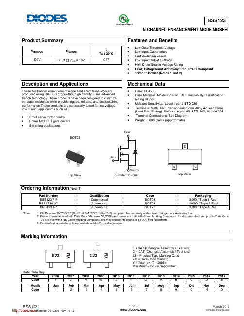
N-CHANNEL ENHANCEMENT MODE MOSFETProduct SummaryV (BR)DSS R DS(ON) I DT A = 25°C 100V6.0Ω @ V GS = 10V0.17Description and Applications These N-Channel enhancement mode field effect transistors are produced using DIODES proprietary, high density, uses advanced trench technology.These products have been designed to minimize on-state resistance while provide rugged, reliable, and fast switchingperformance.These products are particularly suited for low voltage,low current applications such as• Small servo motor control• Power MOSFET gate drivers• Switching applicationsFeatures and Benefits• Low Gate Threshold Voltage • Low Input Capacitance • Fast Switching Speed• Low Input/Output Leakage• High Drain-Source Voltage Rating• Lead, Halogen and Antimony Free, RoHS Compliant • "Green" Device (Notes 1 and 2)Mechanical Data• Case: SOT23 • Case Material: Molded Plastic. UL Flammability Classification Rating 94V-0 • Moisture Sensitivity: Level 1 per J-STD-020• Terminals: Matte Tin Finish annealed over Alloy 42 Leadframe (Lead Free Plating). Solderable per MIL-STD-202, Method 208 • Terminal Connections: See Diagram • Weight: 0.008 grams (approximate)Ordering Information (Note 3)Part Number Qualification Case PackagingBSS123-7-FCommercial SOT23 3,000 / Tape & Reel BSS123Q-13 Automotive SOT23 10,000 / Tape & Reel BSS123Q-7Automotive SOT23 3,000 / Tape & ReelNotes: 1. EU Directive 2002/95/EC (RoHS) & 2011/65/EU (RoHS 2) compliant. No purposely added lead. Halogen and Antimony free.2. Product manufactured with Date Code V9 (week 33, 2008) and newer are built with Green Molding Compound. Product manufactured prior to Date Code V9 are built with Non-Green Molding Compound and may contain Halogens or Sb 2 O 3 Fire Retardants.3. For packaging details, go to our website at Marking InformationDate Code KeyYear 2006 2007 2008 2009 2010 2011 2012 2013 2014 2015 2016 2017Code T U V WX Y Z A B C D EMonth Jan Feb Mar Apr May Jun Jul Aug Sep Oct Nov DecCode 1 2 3 4 5 6 7 8 9 O N DEquivalent Circuit Top View Top View SOT23 GateK = SAT (Shanghai Assembly / Test site) C = CAT (Chengdu Assembly / Test site) 23 = Product Type Marking Code YM = Date Code Marking Y = Year (ex: T = 2006)M = Month (ex: 9 = September)K23Y MC23Y MMaximum Ratings @T A = 25°C unless otherwise specifiedCharacteristicSymbol Value UnitDrain-Source Voltage V DSS 100 V Gate-Source VoltageContinuous V GSS ±20 V Continuous Drain Current (Note 4) V GS = 10V Continuous I D 170mAPulsedI DM680Thermal Characteristics @T A = 25°C unless otherwise specifiedCharacteristic Symbol Max UnitPower Dissipation (Note 4) P D300 mW Thermal Resistance, Junction to Ambient @T A = 25°C (Note 4) R θJA417 °C/W Operating and Storage Temperature Range T J , T STG -55 to +150 °CElectrical Characteristics @ T A = 25°C unless otherwise statedCharacteristicSymbol Min Typ Max Unit Test ConditionOFF CHARACTERISTICS (Note 5) Drain-Source Breakdown Voltage BV DSS 100 - - V V GS = 0V, I D = 250μAZero Gate Voltage Drain Current I DSS - - 0.1 μA V DS = 100V, V GS = 0V - - 10 nA V DS = 20V, V GS = 0V Gate-Source Leakage , Forward I GSSF - - 50 nA V GS = 20V, V DS = 0VON CHARACTERISTICS (Note 5) Gate Threshold VoltageV GS(th)0.8 1.4 2.0 V V DS = V GS , I D = 1mAStatic Drain-Source On-Resistance R DS (ON)- - 6.0 Ω V GS = 10V, I D = 0.17A- - 10 V GS = 4.5V, I D = 0.17AForward Transfer Admittance g FS 80 370 - mS V DS =10V, I D = 0.17A, f = 1.0KHzDiode Forward VoltageV SD - 0.84 1.3 V V GS = 0V, I S = 0.34A, DYNAMIC CHARACTERISTICS Input Capacitance C iss- 29 60 pF V DS = 25V, V GS = 0V, f = 1.0MHzOutput CapacitanceC oss - 10 15 Reverse Transfer CapacitanceC rss - 2 6 SWITCHING CHARACTERISTICS Turn-On Delay Time t D(on) - - 8 ns V GS = 10V, V DD = 30V,I D = 0.28A, R GEN = 50Ω Turn-On Rise Time t r - - 8 ns Turn-Off Delay Time t D(off) - - 13 nsTurn-Off Fall Timet f--16 nsNotes: 4. Part mounted on FR-4 board with recommended pad layout, which can be found on our website at .5. Short duration pulse test used to minimize self-heating effect.I , D R A I N -S O U R C E C U R R E N T (A )D V , DRAIN-SOURCE VOLTAGE (V)Fig. 1 On-Region Characteristics DSR , N O R M A L I Z E D D R A I N -S O U R C E O N -R E S I S T A N C ED S (O N )I , DRAIN-SOURCE CURRENT (A)Fig. 2 On-Resistance Variation with Gate Voltageand Drain-Source Current D0.8V N O R M A L I Z E D T H R E S H O L D V O L T A G EG S (t h ),T , JUNCTION TEMPERATURE (ºC)Fig. 3 Gate Threshold Variation with T emperature J 0.4R N O R M A L I Z E D O N -R E S IS T A N C ED S (O N ),T , JUNCTION TEMPERATURE (ºC)Fig. 4 On-Resistance Variation with Temperature J 0.6C , C A P A C I T A N C E (p F )V , DRAIN-SOURCE VOLTAGE (V)Fig. 5 Typical CapacitanceDSPackage Outline DimensionsSuggested Pad LayoutSOT23Dim Min Max Typ A 0.37 0.51 0.40 B 1.20 1.40 1.30 C 2.30 2.50 2.40 D 0.89 1.03 0.915 F 0.45 0.60 0.535 G 1.78 2.05 1.83 H 2.80 3.00 2.90 J 0.0130.10 0.05 K 0.903 1.10 1.00 K1 - - 0.400 L 0.45 0.61 0.55 M 0.0850.18 0.11α0° 8° - All Dimensions in mmDimensions Value (in mm)Z 2.9 X 0.8 Y 0.9C2.0 E1.35 X EYCZIMPORTANT NOTICEDIODES INCORPORATED MAKES NO WARRANTY OF ANY KIND, EXPRESS OR IMPLIED, WITH REGARDS TO THIS DOCUMENT, INCLUDING, BUT NOT LIMITED TO, THE IMPLIED WARRANTIES OF MERCHANTABILITY AND FITNESS FOR A PARTICULAR PURPOSE (AND THEIR EQUIVALENTS UNDER THE LAWS OF ANY JURISDICTION).Diodes Incorporated and its subsidiaries reserve the right to make modifications, enhancements, improvements, corrections or other changes without further notice to this document and any product described herein. Diodes Incorporated does not assume any liability arising out of the application or use of this document or any product described herein; neither does Diodes Incorporated convey any license under its patent or trademark rights, nor the rights of others. Any Customer or user of this document or products described herein in such applications shall assume all risks of such use and will agree to hold Diodes Incorporated and all the companies whose products are represented on Diodes Incorporated website, harmless against all damages.Diodes Incorporated does not warrant or accept any liability whatsoever in respect of any products purchased through unauthorized sales channel. Should Customers purchase or use Diodes Incorporated products for any unintended or unauthorized application, Customers shall indemnify and hold Diodes Incorporated and its representatives harmless against all claims, damages, expenses, and attorney fees arising out of, directly or indirectly, any claim of personal injury or death associated with such unintended or unauthorized application.Products described herein may be covered by one or more United States, international or foreign patents pending. Product names and markings noted herein may also be covered by one or more United States, international or foreign trademarks.LIFE SUPPORTDiodes Incorporated products are specifically not authorized for use as critical components in life support devices or systems without the express written approval of the Chief Executive Officer of Diodes Incorporated. As used herein:A. Life support devices or systems are devices or systems which:1. are intended to implant into the body, or2. support or sustain life and whose failure to perform when properly used in accordance with instructions for use provided in thelabeling can be reasonably expected to result in significant injury to the user.B. A critical component is any component in a life support device or system whose failure to perform can be reasonably expected to cause thefailure of the life support device or to affect its safety or effectiveness.Customers represent that they have all necessary expertise in the safety and regulatory ramifications of their life support devices or systems, and acknowledge and agree that they are solely responsible for all legal, regulatory and safety-related requirements concerning their products and any use of Diodes Incorporated products in such safety-critical, life support devices or systems, notwithstanding any devices- or systems-related information or support that may be provided by Diodes Incorporated. Further, Customers must fully indemnify Diodes Incorporated and its representatives against any damages arising out of the use of Diodes Incorporated products in such safety-critical, life support devices or systems.Copyright © 2012, Diodes Incorporated分销商库存信息:DIODESBSS123-7-F BSS123-7。
BLF571资料
1.Product profile1.1General descriptionA 20W LDMOS RF transistor for broadcast applications and industrial applications in the HF and VHF band.1.2FeaturesI Typical CW performance at frequency of 225MHz,a supply voltage of 50V and an I Dqof 50 mA:N Average output power =20W N Power gain =27.5dB N Efficiency =70%I Easy power controlI Integrated ESD protection I Excellent ruggedness I High efficiencyI Excellent thermal stabilityI Designed for broadband operation (10 MHz to 500 MHz)I Compliant to Directive 2002/95/EC, regarding Restriction of Hazardous Substances (RoHS)1.3ApplicationsI Industrial, scientific and medical applications I Broadcast transmitter applicationsBLF571HF / VHF power LDMOS transistorRev. 01 — 11 December 2008Preliminary data sheetTable 1.Production test performanceMode of operationf V DS P L G p ηD(MHz)(V)(W)(dB)(%)CW225502027.570CAUTIONThis device is sensitive to ElectroStatic Discharge (ESD). Therefore care should be taken during transport and handling.2.Pinning information[1]Connected to flange.3.Ordering information4.Limiting values5.Thermal characteristicsTable 2.PinningPin Description Simplified outlineGraphic symbol1drain 2gate 3source[1]123sym112132Table 3.Ordering informationType numberPackage NameDescriptionVersion BLF571-flanged LDMOST ceramic package; 2 mounting holes;2leadsSOT467CTable 4.Limiting valuesIn accordance with the Absolute Maximum Rating System (IEC 60134).Symbol ParameterConditionsMin Max Unit V DS drain-source voltage -110V V GS gate-source voltage −0.5+11V I D drain current - 3.6A T stg storage temperature −65+150°C T jjunction temperature-225°CTable 5.Thermal characteristics Symbol ParameterConditionsTyp Unit R th(j-c)thermal resistance from junction to caseT case =80°C; P L =20W2.9K/W6.CharacteristicsTable 6.DC characteristicsT j = 25°C unless otherwise specifiedSymbol Parameter Conditions Min Typ Max UnitV(BR)DSS drain-source breakdownvoltageV GS=0V; I D=0.25mA110--V V GS(th)gate-source threshold voltage V DS=10 V; I D=25mA 1.25 1.7 2.25VV GSq gate-source quiescent voltage V DS=50 V; I D=50mA 1.25 1.75 2.25VI DSS drain leakage current V GS=0V; V DS=50V-- 1.4µAI DSX drain cut-off current V GS=V GS(th)+3.75 V;V DS=10V3.0 3.6-AI GSS gate leakage current V GS=11V; V DS=0V--140nAg fs forward transconductance V DS=10V; I D=1.25A- 1.8-SR DS(on)drain-source on-stateresistance V GS=V GS(th) + 3.75V;I D=833mA- 1.34-ΩC rs feedback capacitance V GS=0V; V DS=50V;f=1MHz-0.18-pFC iss input capacitance V GS=0V; V DS=50V;f=1MHz-22.9-pFC oss output capacitance V GS=0V; V DS=50V;f=1MHz-9.64-pFTable 7.RF characteristicsMode of operation: CW; f=225 MHz; RF performance at V DS=50V; I Dq=50mA; T case=25°C; unless otherwise specified; in a class-AB production test circuitSymbol Parameter Conditions Min Typ Max Unit G p power gain P L = 20 W25.527.529.5dB RL in input return loss P L = 20 W1013-dBηD drain efficiency P L = 20 W6770-%6.1Ruggedness in class-AB operationThe BLF571is capable of withstanding a load mismatch corresponding to VSWR =13:1through all phases under the following conditions: V DS =50V; I Dq =50 mA; P L =20 W;f =225MHz.7.Application information7.1Impedance informationV GS = 0 V; f = 1 MHz.Fig 1.Output capacitance as a function of drain-source voltage; capacitance value without internal matchingV DS (V)05040203010001aaj1722030104050C oss (pF)Table 8.Typical impedanceSimulated Z S and Z L test circuit impedances.f Z S Z L MHz ΩΩ2259.7 + j31.531.7 + j29.3Fig 2.Definition of transistor impedance001aaf059drain Z LZ Sgate7.2ReliabilityTTF (0.1 % failure fraction).(1)T j = 100°C (2)T j = 110°C (3)T j = 120°C (4)T j = 130°C (5)T j = 140°C (6)T j = 150°C (7)T j = 160°C (8)T j = 170°C (9)T j = 180°C (10)T j = 190°C (11)T j = 200°CFig 3.BLF571 electromigration001aaj17310210104103105Y ears 1I DS(DC) (A)0 1.61.20.80.4(1)(2)(3)(4)(5)(6)(7)(8)(9)(10)(11)8.Test information8.1RF performanceThe following figures are measured in a class-AB production test circuit.8.1.11-Tone CWV DS = 50 V; I Dq =50 mA; f = 225 MHz.V DS = 50 V; f =225MHz.(1)I Dq = 20 mA (2)I Dq = 40 mA (3)I Dq = 50 mA (4)I Dq = 60 mA (5)I Dq = 80 mAFig 4.Power gain and drain efficiency as function of load power; typical valuesFig 5.power gain as a function of load power;typical values001aaj174P L (W)03020102515526242830G p (dB)22402060800ηD (%)G pηD001aaj175P L (W)03020102515526242830G p (dB)22(4)(3)(2)(1)(5)8.1.22-Tone CWV DS = 50 V; I Dq =50 mA; f = 225 MHz.(1)P L(1dB) = 43.3 dBm (21.4 W)(2)P L(3dB) = 44 dBm (25.1 W)Fig 6.Load power as function of input power; typical valuesP i (dBm)1321191517001aaj1764446424850P L (dBm)40(1)(2)ideal P LP LV DS = 50 V; I Dq =50 mA; f 1 = 224.95 MHz;f 2=225.05MHz.V DS = 50 V; f 1 = 224.95 MHz; f 2=225.05MHz.(1)I Dq = 20 mA (2)I Dq = 40 mA (3)I Dq = 50 mA (4)I Dq = 60 mA (5)I Dq = 80 mAFig 7.Power gain and drain efficiency as function of peak envelope load power; typical valuesFig 8.Third order intermodulation distortion as a function of peak envelope load power; typical values001aaj177P L(PEP) (W)030201026242830G p (dB)ηD (%)22402060800G pηDP L(PEP) (W)0302010001aaj178−40−200IMD3(dBc)−60(2)(3)(4)(5)(1)8.2Test circuit[1]American Technical Ceramics type 100B or capacitor of same quality.[2]Printed-Circuit Board (PCB): Rogers 5880;εr = 2.2 F/m; height = 0.79 mm; Cu (top/bottom metallization);thickness copper plating =35µm.Table 9.List of componentsAll capacitors should be soldered vertically. For test circuit, see Figure 9 and Figure ponent DescriptionValueRemarksC1, C3, C4,C5, C14multilayer ceramic chip capacitor 100 pF [1]C2multilayer ceramic chip capacitor 39 pF [1]C6multilayer ceramic chip capacitor 68 pF [1]C7, C9multilayer ceramic chip capacitor 1 nF [1]C8multilayer ceramic chip capacitor 4.7 F TDK C4532X7R1E475MT020U or equivalentC10multilayer ceramic chip capacitor 8.2 pF [1]C11electrolytic capacitor470 FC12multilayer ceramic chip capacitor 33 pF [1]C13multilayer ceramic chip capacitor 15 pF [1]L11 turn enamelled copper wireD =5.5mm;d =1mm;length =1mm L2 2 turns enamelled copper wireD =3.5mm;d =1mm;length =3mm L3 5 turns enamelled copper wireD =6mm;d =1mm;length =5mm L4 3.3 turns enamelled copper wireD =3mm;d =1mm;length =4mm L5 3 turns enamelled copper wireD =3mm;d =1mm;length =3mm L6stripline-[2](L × W)16.5mm × 2.4mm L7, L8, L10,L11,L17,L19,L20stripline -[2](L × W)3.0mm × 5.0mmL9stripline -[2](L × W)43.0mm × 2.4mm L12, L15stripline -[2](L × W)3.5mm × 2.4mm L13, L14stripline -[2](L × W)8.0mm × 8.0mm L16stripline -[2](L × W)3.0mm × 5.9mm L18stripline -[2](L × W)27.0mm × 2.4mm L21stripline-[2](L × W)28.5mm × 2.4mmR1metal film resistor1000Ω; 0.6 WFig 9.Class-AB common-source production test circuitC1input50 ΩC14output 50 ΩC8C7V GGR1L13L11L12C6C5L10L2L17L16L4L20L19L5L8L7L1L9L18L21L6L14L3C11C9V DD001aaj179L15C4C3C2C12C13C10Fig ponent layout for class-AB production test circuit001aaj180C11C9C7C8C10C12C6C5C4C2C3C1C13C14L3R1L4L2L1L59 mm NXP BLF571 225 MHz INPUT PCB REV1NXP BLF571 225 MHz OUTPUT PCB REV25.5 mm6.5 mm 5 mm3 mm9.Package outlineFig 11.Package outline SOT467CREFERENCESOUTLINEVERSION EUROPEAN PROJECTIONISSUE DATE IECJEDECEIAJSOT467C99-12-0699-12-280510 mmscaleFlanged LDMOST ceramic package; 2 mounting holes; 2 leads0.150.105.595.339.259.041.651.4018.5417.02DIMENSIONS (millimetre dimensions are derived from the original inch dimensions)3.433.184.673.942.211.96DD 1U 1132AU 2EE 1pbHQFcUNIT Q c D 9.279.02D 1 5.925.77E 5.975.72E 1F H p q mm 0.1840.155inchb 14.2720.4520.19U 2U 1 5.975.720.25w 10.510.0060.0040.2200.2100.3640.3560.0650.0550.730.670.1350.1250.0870.0770.3650.3550.2330.2270.2350.2250.5620.8050.7950.2350.2250.0100.020w 2A M MC CAw 1w 2A B M M MqBSOT467C10.AbbreviationsTable 10.AbbreviationsAcronym DescriptionCW Continuous WaveEDGE Enhanced Data rates for GSM EvolutionGSM Global System for Mobile communicationsHF High FrequencyLDMOS Laterally Diffused Metal-Oxide SemiconductorLDMOST Laterally Diffused Metal-Oxide Semiconductor TransistorRF Radio FrequencyTTF Time T o FailureVHF Very High FrequencyVSWR Voltage Standing-Wave Ratio11.Revision historyTable 11.Revision historyDocument ID Release date Data sheet status Change notice Supersedes BLF571_120081211Preliminary data sheet--12.Legal information12.1Data sheet status[1]Please consult the most recently issued document before initiating or completing a design.[2]The term ‘short data sheet’ is explained in section “Definitions”.[3]The product status of device(s)described in this document may have changed since this document was published and may differ in case of multiple devices.The latest product status information is available on the Internet at URL .12.2DefinitionsDraft —The document is a draft version only. The content is still under internal review and subject to formal approval, which may result in modifications or additions. NXP Semiconductors does not give any representations or warranties as to the accuracy or completeness ofinformation included herein and shall have no liability for the consequences of use of such information.Short data sheet —A short data sheet is an extract from a full data sheet with the same product type number(s)and title.A short data sheet is intended for quick reference only and should not be relied upon to contain detailed and full information. For detailed and full information see the relevant full data sheet, which is available on request via the local NXP Semiconductors sales office. In case of any inconsistency or conflict with the short data sheet, the full data sheet shall prevail.12.3DisclaimersGeneral —Information in this document is believed to be accurate andreliable.However,NXP Semiconductors does not give any representations or warranties,expressed or implied,as to the accuracy or completeness of such information and shall have no liability for the consequences of use of such information.Right to make changes —NXP Semiconductors reserves the right to make changes to information published in this document, including withoutlimitation specifications and product descriptions, at any time and without notice.This document supersedes and replaces all information supplied prior to the publication hereof.Suitability for use —NXP Semiconductors products are not designed,authorized or warranted to be suitable for use in medical, military, aircraft,space or life support equipment, nor in applications where failure ormalfunction of an NXP Semiconductors product can reasonably be expected to result in personal injury, death or severe property or environmentaldamage. NXP Semiconductors accepts no liability for inclusion and/or use of NXP Semiconductors products in such equipment or applications and therefore such inclusion and/or use is at the customer’s own risk.Applications —Applications that are described herein for any of these products are for illustrative purposes only. NXP Semiconductors makes no representation or warranty that such applications will be suitable for the specified use without further testing or modification.Limiting values —Stress above one or more limiting values (as defined in the Absolute Maximum Ratings System of IEC 60134)may cause permanent damage to the device.Limiting values are stress ratings only and operation of the device at these or any other conditions above those given in theCharacteristics sections of this document is not implied. Exposure to limiting values for extended periods may affect device reliability.Terms and conditions of sale —NXP Semiconductors products are sold subject to the general terms and conditions of commercial sale,as published at /profile/terms , including those pertaining to warranty,intellectual property rights infringement and limitation of liability, unless explicitly otherwise agreed to in writing by NXP Semiconductors. In case of any inconsistency or conflict between information in this document and such terms and conditions, the latter will prevail.No offer to sell or license —Nothing in this document may be interpreted or construed as an offer to sell products that is open for acceptance or the grant,conveyance or implication of any license under any copyrights,patents or other industrial or intellectual property rights.Quick reference data —The Quick reference data is an extract of theproduct data given in the Limiting values and Characteristics sections of this document, and as such is not complete, exhaustive or legally binding.12.4TrademarksNotice:All referenced brands,product names,service names and trademarks are the property of their respective owners.13.Contact informationFor more information, please visit:For sales office addresses, please send an email to:salesaddresses@Document status [1][2]Product status [3]DefinitionObjective [short] data sheet Development This document contains data from the objective specification for product development.Preliminary [short] data sheet Qualification This document contains data from the preliminary specification.Product [short] data sheetProductionThis document contains the product specification.14.Contents1Product profile. . . . . . . . . . . . . . . . . . . . . . . . . . 11.1General description. . . . . . . . . . . . . . . . . . . . . . 11.2Features . . . . . . . . . . . . . . . . . . . . . . . . . . . . . . 11.3Applications . . . . . . . . . . . . . . . . . . . . . . . . . . . 12Pinning information. . . . . . . . . . . . . . . . . . . . . . 23Ordering information. . . . . . . . . . . . . . . . . . . . . 24Limiting values. . . . . . . . . . . . . . . . . . . . . . . . . . 25Thermal characteristics. . . . . . . . . . . . . . . . . . . 26Characteristics. . . . . . . . . . . . . . . . . . . . . . . . . . 36.1Ruggedness in class-AB operation. . . . . . . . . . 47Application information. . . . . . . . . . . . . . . . . . . 47.1Impedance information. . . . . . . . . . . . . . . . . . . 47.2Reliability . . . . . . . . . . . . . . . . . . . . . . . . . . . . . 58Test information. . . . . . . . . . . . . . . . . . . . . . . . . 68.1RF performance . . . . . . . . . . . . . . . . . . . . . . . . 68.1.11-T one CW . . . . . . . . . . . . . . . . . . . . . . . . . . . . 68.1.22-T one CW . . . . . . . . . . . . . . . . . . . . . . . . . . . . 78.2T est circuit. . . . . . . . . . . . . . . . . . . . . . . . . . . . . 89Package outline . . . . . . . . . . . . . . . . . . . . . . . . 1010Abbreviations. . . . . . . . . . . . . . . . . . . . . . . . . . 1111Revision history. . . . . . . . . . . . . . . . . . . . . . . . 1112Legal information. . . . . . . . . . . . . . . . . . . . . . . 1212.1Data sheet status . . . . . . . . . . . . . . . . . . . . . . 1212.2Definitions. . . . . . . . . . . . . . . . . . . . . . . . . . . . 1212.3Disclaimers. . . . . . . . . . . . . . . . . . . . . . . . . . . 1212.4T rademarks. . . . . . . . . . . . . . . . . . . . . . . . . . . 1213Contact information. . . . . . . . . . . . . . . . . . . . . 1214Contents. . . . . . . . . . . . . . . . . . . . . . . . . . . . . . 13Please be aware that important notices concerning this document and the product(s)described herein, have been included in section ‘Legal information’.© NXP B.V.2008.All rights reserved.For more information, please visit: For sales office addresses, please send an email to: salesaddresses@Date of release: 11 December 2008。
HT7150-1_PDF_C108066_2017-09-19
Rev. 2.30
6
2014-06-12
HT71xx-1
HT7150-1, +5.0V 输出类型
Ta=25°C
符号
参数
测试条件
VIN
条件
最小 典型 最大
单位
VOUT
输出电压
7V IOUT=10mA
4.850 5.00 5.150
V
IOUT
输出电流
7V
—
20
30
—
mA
∆ VOUT
负载调整率
7V 1mA ≤ IOUT ≤ 30mA
6.4V 无负载
—
2.5
4.0
µA
— 5.4V ≤ VIN ≤ 30V, IOUT=1mA
—
0.1
0.2
%/V
VIN
输入电压
—
—
—
—
30
V
D V OUT D T a´ V O U T
温度系数
6.4V IOUT=10mA, -40°C<Ta<85°C
— ±100 —
ppm/°C
注: 在 VIN = VOUT+2V 与一个固定负载条件下使输出电压下降 2%,此时的输入电压减去输出电压就是 Dropout 电压。
符号
参数
测试条件
VIN
条件
最小 典型 最大
单位
VOUT
输出电压
5.3V IOUT=10mA
3.201 3.300 3.399
V
IOUT
输出电流
5.3V
—
20
30
—
mA
∆ VOUT
负载调整率
5.3V 1mA ≤ IOUT ≤ 30mA
5713中文资料
lOFF
VON
ILK VD lCC(1) lCC(0)
— — — — NOM NOM NOM NOM
MIN OPEN
MIN MIN NOM NOM MAX MAX
2.0 V 2.0 V 0.8 V 0.8 V 0V VCC 5.0 V 0V
0V
80 V
—
0V
80 V
—
0.8 V 150 mA —
0.8 V 300 mA —
Suppression Diode On-State Current,
I O ION . . . . . . . . . . . . . . . . . . . . . . 600 mA D F Power Dissipation at TA = 25°C, PD
FEATURES
s DTL/TTL/PMOS/CMOS Compatible Inputs s Low Input Current s 300 mA Continuous Output Current s Stand-off Voltage of 80 V
Storage Temperature Range,
TS . . . . . . . . . . . . . . . . -55°C to +150°C
*Derate at the rate of 12.5 mW/°C above TA = 25°C.
Always order by complete part number, e.g., UDN5713M .
—
— -50 -100 µA
2
IIN(0)
—
MAX 0.4 V 30 V
—
— -100 -200 µA —
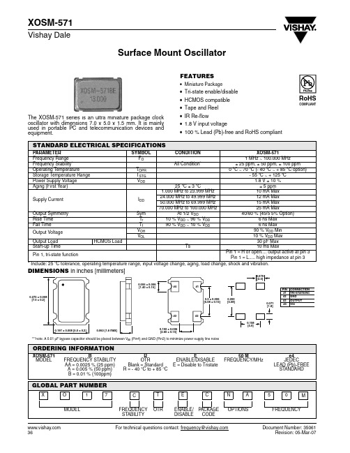
XOSM-571中文资料
ENABLE/ PACKAGE OPTIONS DISABLE CODE
For technical questions contact: frequency@
FREQUENCY
Document Number: 35061 Revision: 05-Mar-07
元器件交易网
Operating Temperature Storage Temperature Range Power Supply Voltage Aging (First Year)
TOPR TSTG VDD
25 ºC ± 3 ºC
0 ºC ~ 70 ºC (- 40 ºC ~ + 85 ºC option) - 55 ºC ~ + 125 ºC 1.8 V ± 10 % ± 5 ppm
Output Symmetry Rise Time Fall Time
Output Voltage
Output Load
HCMOS Load
Sym
Tr Tf VOH VOL
At 1/2 VDD 10 % VDD ~ 90 % VDD 90 % VDD ~ 10 % VDD
40/60 % (45/5 5% Option) 6 ns Max 6 ns Max
E ENABLE/DISABLE E = Disable to Tristate
50 M FREQUENCY/MHz
e4 JEDEC LEAD (Pb)-FREE STANDARD
GLOBAL PART NUMBER
X
O
1
7
C
T
E
C
N
A
5
0
M
MODEL
36
DF56C-26S-0.3V(51);DF56-40S-0.3V(51);DF56-50S-0.3V(51);中文规格书,Datasheet资料
8. Resistance to soldering heat
No deformation of affecting performance
Reflow: At the recommended temperature profile Manual soldering: 350°C for 3 seconds
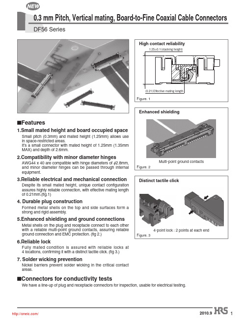
0.3 mm Pitch, Vertical mating, Board-to-Fine Coaxial Cable Connectors
DF56 Series
High contact reliability
1.25±0.1ʢTUBDLJOHIFJHIUʣ
ʢ0.21ʣ&⒎FDUJWFNBUJOHMFOHUI
Figure. 1
Enhanced shielding
■Features
1.Small mated height and board occupied space
Small pitch (0.3mm) and mated height (1.25mm) allows use in space-restricted areas. It’s a small connector with mated height of 1.25mm (1.35mm MAX) and depth of 2.6mm.
4. Durable plug construction
Formed metal shells on the top and side surfaces form a strong and rigid assembly.
5.Enhanced shielding and ground connections
❹ Nomber of positions Standard:20,30,40,50 Connector for conductivity tests : 20.30.40.50
1N5712中文资料
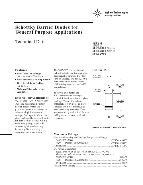
Schottky Barrier Diodes for General Purpose ApplicationsTechnical DataFeatures• Low Turn-On VoltageAs Low as 0.34 V at 1 mA• Pico Second Switching Speed • High Breakdown VoltageUp to 70 V• Matched Characteristics AvailableDescription/Applications The 1N5711, 1N5712, 5082-2800/ 10/11 are passivated Schottky barrier diodes which use a patented “guard ring” design to achieve a high breakdown voltage. Packaged in a low cost glass package, they are well suited for high level detecting, mixing, switching, gating, log or A-D converting, video detecting, frequency discriminating, sampling, and wave shaping.The 5082-2835 is a passivatedSchottky diode in a low cost glasspackage. It is optimized for lowturn-on voltage. The 5082-2835 isparticularly well suited for theUHF mixing needs of the CATVmarketplace.The 5082-2300 Series and5082-2900 devices are unpas-sivated Schottky diodes in a glasspackage. These diodes haveextremely low 1/f noise and areideal for low noise mixing, andhigh sensitivity detecting. Theyare particularly well suited for usein Doppler or narrow band videoreceivers.1N57111N57125082-2300 Series5082-2800 Series5082-2900DIMENSIONS IN MILLIMETERS AND (INCHES).Outline 15Maximum RatingsJunction Operating and Storage Temperature Range5082-2303, -2900.................................................................-60°C to +100°C 1N5711, 1N5712, 5082-2800/10/11....................................-65°C to +200°C 5082-2835............................................................................-60°C to +150°C DC Power Dissipation(Measured in an infinite heat sink at T CASE = 25°C)Derate linearly to zero at maximum rated temperature5082-2303, -2900..............................................................................100 mW 1N5711, 1N5712, 5082-2800/10/11.................................................250 mW 5082-2835.........................................................................................150 mW Peak Inverse Voltage.................................................................................V BRPackage CharacteristicsOutline 15Lead Material........................................................................................DumetLead Finish..............................................................................95-5% Tin-LeadMax. Soldering Temperature................................................260°C for 5 secMin. Lead Strength....................................................................4 pounds pullTypical Package Inductance1N5711, 1N5712:................................................................................2.0 nH2800 Series:........................................................................................2.0 nH2300 Series, 2900:..............................................................................3.0 nHTypical Package Capacitance1N5711, 1N5712:................................................................................0.2 pF2800 Series:........................................................................................0.2 pF2300 Series, 2900:............................................................................0.07 pFThe leads on the Outline 15 package should be restricted so that thebend starts at least 1/16 inch from the glass body.Outline 15 diodes are available on tape and reel. The tape and reelspecification is patterned after RS-296-D.Electrical Specifications at T= 25°CAGeneral Purpose DiodesMin.Max.V F = 1 V Max.Max.Max.Breakdown Forward at Forward Reverse Leakage Capaci-Part Package Voltage Voltage Current Current tance Number Outline V BR (V)V F (mV)I F (mA)I R (nA) at V R (V)C T (pF) 5082-280015704101520050 2.0 1N571115704101520050 2.0 5082-281015204103510015 1.2 1N571215205503515016 1.2 5082-28111515410201008 1.2 5082-2835158*34010*1001 1.0 Test I R = 10 µA I F = 1 mA*V F = 0.45 V V R = 0 V Conditions*I R = 100 µA f =1.0 MHz Note: Effective Carrier Lifetime (τ) for all these diodes is 100 ps maximum measured with Krakauer method at 5 mA except for 5082-2835 which is measured at 20 mA.Low 1/f (Flicker) Noise DiodesMin.Max.V F = 1 V Max.Max.Max.Part Breakdown Forward at Forward Reverse Leakage Capaci-Number Package Voltage Voltage Current Current tance 5082-Outline V BR (V)V F (mV)I F (mA)I R (nA) at V R (V)C T (pF) 230315204003550015 1.0 29001510400201005 1.2 Test I R = 10 µA I F = 1 mA V R = 0 V Conditions f =1.0 MHzNote: Effective Carrier Lifetime (τ) for all these diodes is 100 ps maximum measured with Krakauer method at 20 mA.Matched Pairs and QuadsBasic Matched MatchedPart Number Pair Quad Batch5082-Unconnected Unconnected Matched[1]Test Conditions2900∆VF at IF= 1.0, 10 mA28005082-28045082-2805∆V F at I F = 0.5, 5 mA ∆V F = 20 mV∆V F = 20 mV*I F = 10 mA∆C O at f = 1.0 MHz28115082-2826∆VF at IF= 10 mA∆V F = 10 mV∆C O at f = 1.0 MHz ∆C O = 0.1 pF28355082-2080∆VF at IF=10 mA∆V F = 10 mV∆C O at f = 1.0 MHz∆C O = 0.1 pFNote:1. Batch matched devices have a minimum batch size of 50 devices.SPICE ParametersParameter Units5082-28005082-28105082-28115082-28355082-23035082-2900B V V75251892510C J0pF 1.60.8 1.00.70.7 1.1E G eV0.690.690.690.690.690.69I BV A10E-510E-510E-510E-510E-510E-5I S A 2.2 x 10E-9 1.1 x 10E-90.3 x 10E-8 2.2 x 10E-87 x 1.0E-910E-8N 1.08 1.08 1.08 1.08 1.08 1.08 R SΩ25101051015 P B V0.60.60.60.560.640.64 PT222222 M0.50.50.50.50.50.5Typical ParametersV F – FORWARD VOLTAGE (V)Figure 1. I-V Curve Showing Typical Temperature Variation for 5082-2300 Series and 5082-2900 Schottky Diodes.1001010.10.01I F - F O R W A R D C U R R E N T (m A )V BR (V)Figure 2. 5082-2300 Series Typical Reverse Current vs. Reverse Voltage at Various Temperatures.10.0001,000100101I R (n A )051015100755025T A = 25°CI F - FORWARD CURRENT (mA)Figure 3. 5082-2300 Series and 5082-2900 Typical Dynamic Resistance (R D ) vs. Forward Current (I F ).100010010R D - D Y N A M I C R E S I S T AN C E (Ω)0.01010100V R - REVERSE VOLTAGE (V)Figure 4. 5082-2300 and 5082-2900 Typical Capacitance vs. Reverse Voltage.1.21.00.80.60.40.20C T - C A P A C I T A N C E (p F )048121620V F - FORWARD VOLTAGE (V)Figure 5. I-V Curve Showing Typical Temperature Variation for 5082-2800 or 1N5711 Schottky Diodes.5010510.50.10.050.01I F - F O R W A R D C U R R E N T (m A )00.20.40.60.8 1.0 1.2V R - REVERSE VOLTAGE (V)Figure 6. (5082-2800 OR 1N5711) Typical Variation of Reverse Current (I R ) vs. Reverse Voltage (V R ) at Various Temperatures.100,00010,0001000100101I R - R E V E R S E C U R R E N T (n A )0.20.40.60.81.01.2V R - REVERSE VOLTAGE (V)Figure 7. (5082-2800 or 1N5711)Typical Capacitance (C T ) vs. Reverse Voltage (V R ).12.01.51.00.50C T - C A P A C I T A N C E (p F )010********V F - FORWARD VOLTAGE (V)Figure 8. I-V Curve Showing Typical Temperature Variation for the 5082-2810 or 1N5712 Schottky Diode.100101.00.10.01I F - F O R W A R D C U R R E N T (m A )V R - REVERSE VOLTAGE (V)Figure 9. (5082-2810 or IN5712)Typical Variation of Reverse Current (I R ) vs. Reverse Voltage (V R ) at Various Temperatures.10,0001000100101.0I R - R E V E R S E C U R R E N T (n A )Typical Parameters, continuedV F - FORWARD VOLTAGE (V)Figure 10. I-V Curve Showing Typical Temperature Variation for the 5082-2811 Schottky Diode.100101.00.10.01I F - F O R W A R D C U R R E N T (m A )0.40.20.60.81.01.2V R - REVERSE VOLTAGE (V)Figure 11. (5082-2811) Typical Variation of Reverse Current (I R ) vs. Reverse Voltage (V R ) at Various Temperatures.100,00010,0001000100101I R - R E V E R S E C U R R E N T (n A )0510********V F - FORWARD VOLTAGE (V)Figure 12. I-V Curve Showing Typical Temperature Variations for 5082-2835 Schottky Diode.100101.00.10.01I F - F O R W A R D C U R R E N T (m A )00.20.40.60.8 1.0 1.2V R - REVERSE VOLTAGE (V)Figure 13. (5082-2835) Typical Variation of Reverse Current (I R ) vs. Reverse Voltage (V R ) at Various Temperatures.100,00010,0001000100101I R - R E V E R S E C U R R E N T (n A )0123456V R - REVERSE VOLTAGE (V)Figure 14. Typical Capacitance (C T ) vs. Reverse Voltage (V R ).C T - C A P A C I T A N C E (p F )0246810I F - FORWARD CURRENT (mA)Figure 15. Typical Dynamic Resistance (R D ) vs. Forward Current (I F ).1000100101R D - D Y N A M I C R E S I S T A N C E (Ω)Diode Package Marking1N5xxx5082-xxxxwould be marked:1Nx xxxxx xxYWW YWWwhere xxxx are the last four digits of the 1Nxxxx or the 5082-xxxx partnumber. Y is the last digit of the calendar year. WW is the work week ofmanufacture.Examples of diodes manufactured during workweek45 of 1999:1N57125082-3080would be marked:1N53071280945945Data subject to change.Copyright © 1999 Agilent TechnologiesObsoletes 5968-4304E5968-7181E (11/99)。
TEA5711中文资料
• Designed for simple and reliable printed-circuit board layout
• High impedance MOSFET input on AM.
APPLICATIONS • Portable AM/FM stereo radio • Mini/midi receiver sets • Personal headphone radio.
SYMBOL
PARAMETER
CONDITIONS
MIN.
VP
dynamic supply voltage
1.8
VP
static supply voltage
2.1
IP
supply current
AM mode
11.9
FM mode
13.5
Tamb
operating ambient temperature
September 1994
2
Philips Semiconductors
AM/FM stereo radio circuit
BLOCK DIAGRAM
September 1994
元器件交易网Thwiswtewx.tcisechber2ebi.ncwohmite to force landscape pages to be rotated correctly when browsing through the pdf in the Acrobat reader.This text is here in
PIN
DESCRIPTION
1 not connected 2 left channel audio output (output impedance typ. 4.3 kΩ) 3 right channel audio output (output impedance typ. 4.3 kΩ) 4 pilot detector filter pin
SQT-103-01-F-D;SQT-106-01-LM-D;SQT-110-03-F-D;SQT-120-01-F-S;中文规格书,Datasheet资料
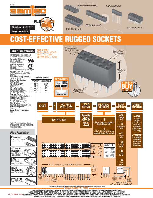
SPECIFICATIONS
For complete specifications see ?SQT
Mates with: TMMH, TMM, MTMM, MMT, TW, LTMM, ZLTMM, ESQT, TCMD
Choice of one through six rows
SQT-106-01-LM-D SQT-112-01-F-D SQT-110-01-L-Q
SQT-110-03-F-D SQT-107-01-L-T SQT-125-01-F-D
(2,29) .050 .090
(2,00) .0787
–RA OPTION
(–Q, –5 & –6 not available)
/
分销商库存信息:
SAMTEC SQT-103-01-F-D SQT-120-01-F-S SQT-110-01-LM-Q SQT-116-01-S-D
TMM/ SQT TMMH
HORIZONTAL
(2,00mm) .0787" pitch
1
NO. PINS PER ROW
LEAD STYLE
(6,35mm) .250"
PLATING OPTION
ROW OPTION
Note: Some lengths, styles and options are non-standard, non-returnable.
20°C
5.5A
(2,62mm) .103" to (5,03mm) .198" Insertion Force: (Single contact only)
40°C
5A
60°C
CN5710规格书CN5710PDF

高亮度发光二极管(LED)驱动集成电路CN5710概述:CN5710是一款电流调制集成电路, 恒定输出电流可达1A ,可以用来驱动包括白色发光二极管在内的各类发光二极管。
CN5710的LED 端电流通过一个外部的电阻设置,电流范围为30mA 到1A 。
芯片内部集成有功率晶体管,大大减少了外部元器件的数目。
其它功能包括芯片温度调制,芯片使能输入端等。
CN5710具有外围元器件少,使用方便,可实现多种模式调光,效率高等优点,非常适合便携式产品的应用。
CN5710采用5管脚SOT89封装。
应用:● 手电筒● 高亮度发光二极管(LED)驱动 ● 发光二极管(LED)头灯 ●应急灯及照明灯具特点:● 工作电压范围:2.8V 到 6V ● 芯片内部集成有功率晶体管 ● 低压差:0.25V@800mA ● LED 管脚输出电流可达1A ● 输出电流精度:±5% ● 芯片温度调制功能 ● 过流保护功能● 工作环境温度范围:-40℃到85℃ ● 采用5管脚的SOT89封装● 产品无铅,满足rohs 指令要求,无卤素管脚排列图:CE LEDGND ISET深圳市国兴顺电子有限公司郑海鑫 139****1192Q Q 514789807●●典型应用电路:图1 典型应用电路订购信息:器件型号 封装形式 包装工作环境温度 CN5710 SOT89-5 盘装,每盘1000只-40℃ 到 85℃功能框图:ISET LED图2 功能框图管脚描述:序号.名称功能描述1 CE芯片使能输入端。
输入高电平使CN5710处于正常工作状态;输入低电平使CN5710处于禁止工作状态。
CE 管脚可以被TTL 电平或者CMOS 电平驱动。
2 GND 电源地3 ISET LED 电流设置端。
LED 电流设置是通过在ISET 管脚和地之间连接一个电阻R ISET 实现的,计算电流的公式如下:I LED = 1800V /R ISET其中, I LED 的单位是安培(A)R ISET 的单位是欧姆(Ω)。
2SC5712(TE12L,F);中文规格书,Datasheet资料
♦: Single nonrepetitive pulse
Ta = 25°C 0.1 Note that the curves for 100 ms*,
10 s* and DC operation* will be
different when the devices aren’t
mounted on an FR4 board (glass
Unit: mm
• High DC current gain: hFE = 400 to 1000 (IC = 0.3 A) • Low collector-emitter saturation voltage: VCE (sat) = 0.14 V (max) • High-speed switching: tf = 120 ns (typ.)
Note 2: Using continuously under heavy loads (e.g. the application of high temperature/current/voltage and the significant change in temperature, etc.) may cause this product to decrease in the reliability significantly even if the operating conditions (i.e. operating temperature/current/voltage, etc.) are within the absolute maximum ratings. Please design the appropriate reliability upon reviewing the Toshiba Semiconductor Reliability Handbook (“Handling Precautions”/“Derating Concept and Methods”) and individual reliability data (i.e. reliability test report and estimated failure rate, etc).
S-80831中文资料

Hysteresis characteristics
5% typ.
Detection voltage
0.8 to 6.0 V (0.1 V step)
Nch open-drain active low and CMOS active low output SC-82AB Super-small plastic package TO-92 Plastic package SOT-89-3 Miniaturized power mold plastic package SOT-23-5 Very-small plastic package
Battery checker Power failure detector Power monitor for pagers, calculators,
organizers,
Constant voltage power monitor for cameras,
video equipment, communication devices
OUT VDD NC VSS
1 2 3
OUT VDD VSS
1 Bottom view
2
3
1
2
3
Figure 1
Seiko InstrALL PACKAGE HIGH-PRECISION VOLTAGE DETECTOR S-808 Series
2
Seiko Instruments Inc.
易网
SUPER-SMALL PACKAGE HIGH-PRECISION VOLTAGE DETECTOR S-808 Series
Table 1
Detection voltage range (V) 0.8V±2.0% 0.9V±2.0% 1.0V±2.0% 1.1V±2.0% 1.2V±2.0% 1.3V±2.0% 1.4V±2.0% 1.5V±2.0% 1.6V±2.0% 1.7V±2.0% 1.8V±2.0% 1.9V±2.0% 2.0V±2.0% 2.1V±2.0% 2.2V±2.0% 2.3V±2.0% 2.4V±2.0% 2.5V±2.0% 2.6V±2.0% 2.7V±2.0% 2.8V±2.0% 2.9V±2.0% 3.0V±2.0% 3.1V±2.0% 3.2V±2.0% 3.3V±2.0% 3.4V±2.0% 3.5V±2.0% 3.6V±2.0% 3.7V±2.0% 3.8V±2.0% 3.9V±2.0% 4.0V±2.0% 4.1V±2.0% 4.2V±2.0% 4.3V±2.0% 4.4V±2.0% 4.5V±2.0% 4.6V±2.0% 4.7V±2.0% 4.8V±2.0% 4.9V±2.0% 5.0V±2.0% 5.1V±2.0% 5.2V±2.0% 5.3V±2.0% 5.4V±2.0% 5.5V±2.0% 5.6V±2.0% 5.7V±2.0% 5.8V±2.0% 5.9V±2.0% 6.0V±2.0% Hysteresis width VHYS typ.(V) 0.034 0.044 0.054 0.064 0.073 0.083 0.093 0.075 0.080 0.085 0.090 0.095 0.100 0.105 0.110 0.115 0.120 0.125 0.130 0.135 0.140 0.145 0.150 0.155 0.160 0.165 0.170 0.175 0.180 0.185 0.190 0.195 0.200 0.205 0.210 0.215 0.220 0.225 0.230 0.235 0.240 0.245 0.250 0.255 0.260 0.265 0.270 0.275 0.280 0.285 0.290 0.295 0.300 Nch Open Drain(Low) SC-82AB S-80808ANNP-E7Y-T2 S-80809ANNP-E7Z-T2 S-80810ANNP-E70-T2 S-80811ANNP-E71-T2 S-80812ANNP-E72-T2 S-80813ANNP-EDA-T2 S-80814ANNP-EDB-T2 S-80815ANNP-EDC-T2 S-80816ANNP-EDD-T2 S-80817ANNP-EDE-T2 S-80818ANNP-EDF-T2 S-80819ANNP-EDG-T2 S-80820ANNP-EDH-T2 S-80821ANNP-EDJ-T2 S-80822ANNP-EDK-T2 S-80823ANNP-EDL-T2 S-80824ANNP-EDM-T2 S-80825ANNP-EDN-T2 S-80826ANNP-EDP-T2 S-80827ANNP-EDQ-T2 S-80828ANNP-EDR-T2 S-80829ANNP-EDS-T2 S-80830ANNP-EDT-T2 S-80831ANNP-EDV-T2 S-80832ANNP-EDW -T2 S-80833ANNP-EDX-T2 S-80834ANNP-EDY-T2 S-80835ANNP-EDZ-T2 S-80836ANNP-ED0-T2 S-80837ANNP-ED1-T2 S-80838ANNP-ED2-T2 S-80839ANNP-ED3-T2 S-80840ANNP-ED4-T2 S-80841ANNP-ED5-T2 S-80842ANNP-ED6-T2 S-80843ANNP-ED7-T2 S-80844ANNP-ED8-T2 S-80845ANNP-ED9-T2 S-80846ANNP-EJA-T2 S-80847ANNP-EJB-T2 S-80848ANNP-EJC-T2 S-80849ANNP-EJD-T2 S-80850ANNP-EJE-T2 S-80851ANNP-EJF-T2 S-80852ANNP-EJG-T2 S-80853ANNP-EJH-T2 S-80854ANNP-EJJ-T2 S-80855ANNP-EJK-T2 S-80856ANNP-EJL-T2 S-80857ANNP-EJM-T2 S-80858ANNP-EJN-T2 S-80859ANNP-EJP-T2 S-80860ANNP-EJQ-T2 TO-92 — — — — — — — S-80815ANY S-80816ANY S-80817ANY S-80818ANY S-80819ANY S-80820ANY S-80821ANY S-80822ANY S-80823ANY S-80824ANY S-80825ANY S-80826ANY S-80827ANY S-80828ANY S-80829ANY S-80830ANY S-80831ANY S-80832ANY S-80833ANY S-80834ANY S-80835ANY S-80836ANY S-80837ANY S-80838ANY S-80839ANY S-80840ANY S-80841ANY S-80842ANY S-80843ANY S-80844ANY S-80845ANY S-80846ANY S-80847ANY S-80848ANY S-80849ANY S-80850ANY S-80851ANY — S-80853ANY — — — — — — — SOT-89-3 — — — — — — — S-80815ANUP-EDC-T2 S-80816ANUP-EDD-T2 S-80818ANUP-EDF-T2 SOT-23-5 — — — — — — — — — S-80818ANMP-EDF-T2
M57140-01;中文规格书,Datasheet资料
VIN
Direct Current
VO
Between Pins 10 - 9 , 12 - 11, 14 - 13,
IL = 30mA
Between Pins 8 - 7 , IL = 100mA
ILP
Between Pins 10 - 9 , 12 - 11, 14 - 13
Between Pins 8 - 7
Load Regulation Efficiency
Reg-out h
Between Pins 10 - 9 , 12 - 11, 14 - 13, IL = 0 ~ 30mA
Between Pins 8 - 7 , IL = 0 ~ 100mA Between Pins 10 - 9 , 12 - 11, 14 - 13,
IL = 30mA Between Pins 8 - 7 , IL = 100mA
Min. 18 13.5
13.5 – – –
– –
–
Typ. 20 15.0
Max. 22 16.5
Units Volts Volts
15.0 16.5
33
–
110
–
5 10
Volts mA mA %
7 12
%
70
–
%
159 /
Powerex, Inc., 200 Hillis Street, Youngwood, Pennsylvania 15697-1800 (724) 925-7272
M57140-01 Isolated DC-to-DC Converter
Absolute Maximum Ratings, VIN = 20V, Ta = 25 °C unless otherwise specified
28130;中文规格书,Datasheet资料
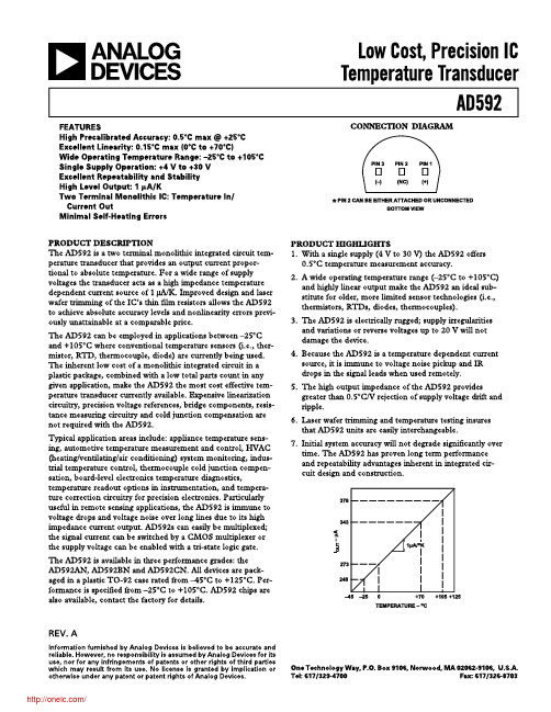
METALIZATION DIAGRAM
TEMPERATURE SCALE CONVERSION EQUATIONS
+2.0 +1.5 +1.0 +0.5
0 –0.5 –1.0 –1.5 –2.0
–25
0
+25
+70
TEMPERATURE – oC
+105
AD592BN Accuracy Over Temperature
TOTAL ERROR – oC TOTAL ERROR – oC
+2.0 +1.5 +1.0 +0.5
+1.0
+0.5
MAXIMUM ERROR OVER TEMPERATURE
TYPICAL ERROR
0 CALIBRATION ERROR LIMIT
–0.5
TOTAL ERROR – oC
IOUT – µA
378
+105oC
298
+25oC
–25oC 248
UP TO 30V
0
1
2
3
4
5
6
SUPPLY VOLTAGE – Volts
66MILS
V+
V–
/
Model
AD592CN AD592BN AD592AN
42MILS
؇C = 5 (؇F –32) 9
S-5716系列 霍尔IC
(除特殊注明以外 : Ta = +25°C)
绝对最大额定值
单位
VSS − 0.3 ~ VSS + 7.0
V
±2.0
mA
VSS − 0.3 ~ VSS + 7.0
V
VSS − 0.3 ~ VDD + 0.3
V
430*1
mW
300*1
mW
−40 ~ +85
°C
−40 ~ +125
°C
注意 绝对最大额定值是指无论在任何条件下都不能超过的额定值。万一超过此额定值,有可能造成产品劣化等 物理性损伤。
50.50 ms (典型值) CMOS出力
S-5716ACDH1-I4T1U
50.50 ms (典型值) CMOS出力
S-5716ACDH2-I4T1U
50.50 ms (典型值) CMOS出力
S-5716ACSL0-I4T1U
50.85 ms (典型值) CMOS出力
S-5716ACSL1-I4T1U
磁性灵敏度 (BOP) 1.8 mT (典型值) 3.0 mT (典型值) 4.5 mT (典型值) 7.0 mT (典型值) 1.8 mT (典型值) 3.0 mT (典型值) 4.5 mT (典型值)
3. 1. 2 CMOS输出产品
表3
产品名
驱动周期 (tCYCLE)
输出方式
S-5716ACDL0-M3T1U
50.50 ms (典型值) N沟道开路漏极输出
S-5716ANDL2-M3T1U
50.50 ms (典型值) N沟道开路漏极输出
S-5716ANDL3-M3T1U
50.50 ms (典型值) N沟道开路漏极输出
AD571中文资料

REV. A
Information furnished by Analog Devices is believed to be accurate and reliable. However, no responsibility is assumed by Analog Devices for its use, nor for any infringements of patents or other rights of third parties which may result from its use. No license is granted by implication or otherwise under any patent or patent rights of Analog Devices.
3. The AD571 accepts either unipolar (0 V to +10 V) or bipolar (–5 V to +5 V) analog inputs by grounding or opening a single pin.
4. The device offers true 10-bit accuracy and exhibits no missing codes over its entire operating temperature range.
ANALOG INPUT IMPEDANCE
–
SFH5711中文资料

SFH 5711Hochgenauer Umgebungslichtsensor High Accuracy Ambient Light SensorLead (Pb) Free Product - RoHS Compliant 2007-04-031Wesentliche Merkmale•Optohybrid mit logarithmischem Stromausgang •Perfekt an die Augenempfindlichkeit (V λ) angepasst•Niedriger Temperaturkoeffizient der Fotoempfindlichkeit•Hohe Genauigkeit über weiten Beleuchtungsstärkebereich •Automotive Freigabe Anwendungen •Anwendungen im Automobilbereich •Sonnenlichtsensor / Fahrlichtkontrolle •Steuerung von Displayhinterleuchtungen •Mobile GeräteTyp TypeBestellnummer Ordering codeAusgangsstrom , E v = 1000lx, (white LED LW 541C) Output current , I OUT / μA SFH 5711-2/31)1)Nur eine Gruppe innerhalb einer Verpackungseinheit, siehe Kenndaten. Only one bin within one packing unit, see characteristicsQ65110A451327 - 32SFH 5711-1/21)on request 25 - 30SFH 5711-3/41)on request29 - 34Features•Opto hybrid with logarithmic current output •Perfect match to Human Eye Sensitivity (V λ) •Low temperature coefficient of spectral sensitivity•High accuracy over wide illumination range •Automotive qualified Applications •Automotive applications•Sunlight sensor / head lamp control •Control of display backlighting •Mobile devices2007-04-032GrenzwerteMaximum Ratings Bezeichnung ParameterSymbol SymbolWert Value Einheit Unit Betriebs- und LagertemperaturOperating and storage temperature range T stg – 40 … + 1001)1)Maximum operation temperature of 100°C is only valid after soldering with JEDEC level 4 preconditioning. With JEDEC level 3 max. preconditioning operating temperature is 85°C.°C Versorgungsspannung Supply voltage V CC6V Ausgangsspannung Output voltageV OUT< V CC V Elektrostatische Entladung Electrostatic dischargeHuman Body Model according to EOS/ESD-5.1-1993ESD 2kVEmpfohlener ArbeitsbereichRecommended Operating Conditions Bezeichnung Parameter Symbol SymbolWert Value Einheit Unitmin.typ.max.Betriebsspannung Supply voltageV CC 2.35.5V Beleuchtungsstärke IlluminanceT A = – 30 °C ... + 70 °C T A = – 40 °C ... + 100 °CE V3 ... 80k 10...80klxA CharacteristicsBezeichnung Parameter SymbolSymbolWertValueEinheitUnitmin.typ.max.Stromaufnahme, E V = 0 Current consumptionV CC = 2.5 VV CC = 5.0 V ICC410420500μAStromaufnahme, E V = 1000lx Current consumption, E V = 1000lx V CC = 2.5 VV CC = 5.0 V ICC460470550μASpektraler Bereich der Fotoempfindlichkeit Spectral range of sensitivity λ10%475 ...650nmWellenlänge der max. FotoempfindlichkeitWavelength of max. photosensitivityλs max540555570nmAbmessung der bestrahlungsempfindlichen FlächeDimensions of radiant sensitive area L x BL x W0.4 x0.4mm x mmAusgangskapazitätOutput capacitanceC OUT3pFTransferfunktion Transfer function, s. Fig. 1G9.51010.5µA / dekµA / decAbweichung der Ausgangskennlinie von derLogarithmierfunktionDeviation of outputcharacteristic from logarithmicfunction, s. Fig. 1L- 3+ 3%Maximale Ausgangsspannung Maximum output voltage V OUT V CC- 0.5VEinschaltzeit, E V = 1000 lx Power on time, E V = 1000 lx V CC = 0V -> V CC tON0.1 1.2msAntwortzeit, R L = 25 kOhm, C = 1 nF Response time, s. Fig. 2E V = 100 -> 1000 lxE V = 1000 -> 100 lx tr/ t f0.030.1ms2007-04-0332007-04-034Figure 1Ersatzschaltbild CircuitryAusgangsgenauigkeit über Temperaturbereich 1) Output accuracy over temperature range 1) E V = 1000 lxT A = – 40 °C ... + 100 °C T A = – 30 °C ... + 70 °C T A = 0 °C ... + 50 °CΔI OUT− 2.0 − 1.5 − 0.7± 1.0 ± 0.6 ± 0.2+ 2.0 + 1.5 + 0.7µAAusgangsdunkelstrom, E V = 0 Output dark currentI out0.1100nA1)Diese Werte entsprechen einer Photodiode mit einem TC von ungefähr 0.3 %/K. These values correspond to a photodiode with a TC of approximately 0.3 %/K.Gruppierung (T A = 25 °C) Binning Bezeichnung ParameterSymbol SymbolWert Value Einheit Unit-1-2-3-4Ausgangsstrom 1) Output current E V = 1000lx (white LED LW 541C)1)3µA Gruppenbreite entspricht einem Verhältnis von 1:2 in der Bestrahlungsstärke. 3µA bin width is equivalent to a spread of 1:2 of the irradiance.I out 25 ... 2827 (30)29 (32)31 (34)μAA Characteristics Bezeichnung ParameterSymbol SymbolWert Value Einheit Unit min.typ.max.Figure 2Definition der AntwortzeitDefinition of Response Time 2007-04-0352007-04-036Relative Spectral Sensitivity of photodiodeOutput Current I= f (E )Directional Characteristics of photodiode = ()Current Consumption IMaßzeichnungPackage OutlinesMaße in mm (inch) / Dimensions in mm (inch)AnschlußbelegungPin configurationPin #Description1GND2GND3V CC4I OUT2007-04-037Empfohlenes LötpaddesignRecommended Solderpad DesignMaße in mm (inch) / Dimensions in mm (inch)2007-04-0382007-04-039LötbedingungenVorbehandlung nach JEDEC Level 3 Soldering ConditionsPreconditioning acc. to JEDEC Level 3Reflow Lötprofil für bleifreies Löten(nach J-STD-020C) Reflow Soldering Profile for lead free soldering(acc. to J-STD-020C)Published byOSRAM Opto Semiconductors GmbHWernerwerkstrasse 2, D-93049 Regensburg © All Rights Reserved.The information describes the type of component and shall not be considered as assured characteristics.Terms of delivery and rights to change design reserved. Due to technical requirements components may contain dangerous substances. For information on the types in question please contact our Sales Organization.PackingPlease use the recycling operators known to you. We can also help you – get in touch with your nearest sales office. By agreement we will take packing material back, if it is sorted. You must bear the costs of transport. For packing material that is returned to us unsorted or which we are not obliged to accept, we shall have to invoice you for any costs incurred.Components used in life-support devices or systems must be expressly authorized for such purpose! Critical components 1 , may only be used in life-support devices or systems 2 with the express written approval of OSRAM OS.1A critical component is a component usedin a life-support device or system whose failure can reasonably be expected to cause the failure of that life-support device or system, or to affect its safety or effectiveness of that device or system.2Life support devices or systems are intended (a) to be implanted in the human body, or (b) to support and/or maintain and sustain human life. If they fail, it is reasonable to assume that the health of the user may be endangered.。