Structural and Electrical Properties of Metal Silicide Precipitates in Silicon
“第17届凝聚态理论与统计物理学术会议”日程(初稿)

吴超(西安交通大学) 题目: The influence of local arrangements of oxygen adatoms on the energetics of O2 dissociation over Pt(111) 赵明文(山东大学) 题目: 新型碳材料结构设计和性能调控的理 论模型 李希茂(北京宏剑公司)(12:10-12:25) 题目: 第一原理计算材料的缺陷和掺杂特性
李文飞(南京大学) 题目: 蛋白质分子体系多尺度理论模拟
孙久勋(电子科技大学) 题目: Improvement of unified mobility model and electrical properties for organic diodes under dc and ac conditions
关丽(河北大学):Structural stability and electronic properties of two nonstoichiometric SrTiO3 phases
休息
报告厅 3(主题: 冷原子物理) 分会报告 ST3.3 主席:成 泽 教授(华中科技大学) (邀请报告) 周琦(香港中文大学) 题目:自旋轨道耦合下波色凝聚体的命运
主席:金国钧 教授(南京大学)
(邀请报告) 杨义峰(中国科学院物理研究所) (邀请报告) 孟胜(中国科学院物理研究所)
题目:重费米子物理中的演生现象
题目:Energy Conversion At Nanoscale
张胜利-TheHGI-南京理工大学
张胜利邮箱:zhangslvip@通讯地址:南京市玄武区孝陵卫200号材料科学与工程学院,邮编:210094主要研究方向:1.二维半导体精细结构的XAFS实验和模拟相结合的研究;2.新型光电信息功能材料的设计和电子结构性质研究;3.低维纳米材料结构与物理化学性质的第一性原理研究。
主持科研项目:1. 国家自然科学青年基金项目,过渡金属二硫属化物范德华异质结的组装、能带调控和光学性质研究,2015.1-2017.12,主持(在研)。
2. 江苏省科技计划项目-青年项目,类石墨烯TMDCs范德华异质结能带调控和光学性质研究,2014.7-2017.6,主持(在研)。
3. 中国博士后科研资助计划项目(2014M551594),过渡金属二硫属化物范德华异质结的理论设计与物性调控,2014.9-2016.9,主持(在研)。
4. 江苏省博士后科研资助计划项目(1402154C),新型二维VIB族硫属化合物层状复合材料的设计和性能调控,2014.11-2016.11,主持(在研)。
研究工作经历:2013/7-至今,南京理工大学,材料科学与工程学院,讲师;2008/09 – 2013/06 北京化工大学,计算材料方向, 博士。
教学工作:《新材料技术概论》,《纳米CMOS集成电路设计与加工》和《半导体器件TCAD设计》代表性学术论文:2014Antimonene: Semimetal-semiconductor and Indirect-direct Band Gap Transitions, Angewandte Chemie International Edition, 2014, Accepted. (IF=11.336)phase transition between metallic and semiconducting single-layer MoS2 and WS2 through size effects, Physical Chemistry Chemical Physics 2014, On-line, DOI: 10.1039/c4cp04775c. (IF=4.198)storage for B/n-codoped graphyne, RSC Advances, 4, 54879, 2014. (IF=3.708)24. Yousheng Zou, Haipeng Wang, Shengli Zhang, Dong Lou, Yuhui Dong, Xiufeng Song, Haibo Zeng. Structural, electrical and optical properties of Mg-doped CuAlO 2 films by pulsed laser deposition. RSC Advances, 4, 41294, 2014. (IF=3.708)23. Xiaoming Li, Shengli Zhang, Sergei A Kulinich, Yanli Liu, Haibo Zeng. Engineering surface states ofcarbon dots to achieve controllable luminescence for solid-luminescent composites and sensitiveBe2+ detection. Scientific Reports, 4, 4976-4983, 2014. (IF=5.078)22. Lihong Zhang, Shengli Zhang, Peng Wang, Chuan Liu, Shiping Huang, Huiping Tian. The effect of electric field on Ti-decorated graphyne for hydrogen storage. Computational and Theoretical Chemistry, 1035, 68-75, 2014. (IF=1.368)21. Xiaoli Du, Chuan Liu, Shengli Zhang, Peng Wang, Shiping Huang, Huiping Tian. Structural, magnetic and electronic properties of FenPt13-n clusters with n=0-13: A first-principle study. Journal of Magnetism and Magnetic Materials, 369, 27-33, 2014. (IF=2.002)201320. Shengli Zhang, Yonghong Zhang, Shiping Huang, Peng Wang, Huiping Tian. First-principles study of cubane-type ZnO: Another ZnO polymorph. Chemical Physics Letters, 556, 102-105, 2013.(IF=1.991)19. Shengli Zha ng, Yonghong Zhang, Shiping Huang, Peng Wang and Huiping Tian. Mechanistic investigations on the adsorption of thiophene over cubane–type Zn3NiO4 bimetallic oxide. Applied Surface Science, 258, 10148-10153, 2013. (IF=2.538)18. Chuan Liu, Shengli Zhang, Shiping Huang, Peng Wang, Huiping Tian. Structure, electronic characteristic and thermodynamic properties of K2ZnH4 hydride crystal: A first–principles study.Journal of Alloys and Compounds, 549, 30-37, 2013. (IF=2.726)17. Jia Li, Shengli Zhang, Shiping Huang, Peng Wang, Huiping Tian. Structural, electronic and thermodynamic properties of R3ZnH5(R=K, Rb, Cs): A first–Principle calculation. Journal of Solid State Chemistry, 198, 433-439, 2013. (IF=2.200)16. Zheng Wu, Yonghong Zhang, Shiping Huang, Shengli Zhang. The structural and electronic properties of assembled CdTe Multi–cage nanochains. Computational Materials Science, 68, 238-244, 2013. (IF=1.879)15. Peng Wang, Mingxia Yang, Shengli Zhang, Shiping Huang, Huiping Tian. Density functional theory study of the electronic and magnetic properties of Mn–doped (MgO)n (n=2–10) clusters. Chinese Journal Chemical Physics, 1, 35-42, 2013. (IF=0.720)14. Jiali Jiang, Shengli Zhang, Shiping Huang, Peng Wang, Huiping Tian. Density functional theory studies of Yb-, Ca- and Sr-substituted Mg2NiH4 hydrides. Computational Materials Science, 7, 55-64, 2013. (IF=1.879)13. Ping Cheng, Shengli Zhang, Peng Wang, Shiping Huang, Huiping Tian. First-principles investigation of thiophene adsorption on Ni13 and Zn@Ni12 putational and Theoretical Chemistry, 1020, 136-142, 2013. (IF=1.368)12. Chuan Liu, Shengli Zha ng, Peng Wang, Shiping Huang, Huiping Tian. Confinement effects on structural, electronic properties and dehydrogenation thermodynamics of LiBH4. International Journal of Hydrogen Energy, 20, 8367-8375, 2013. (IF=2.930)11. Yonghong Zhang, Hui Ding, Chuan Liu, Shengli Zhang, Shiping Huang. Significant effects of graphite fragments on hydrogen storage performances of LiBH4: A first-principlesapproach. International Journal of Hydrogen Energy, 38, 13717-13727, 2013. (IF=2.930)201210. Shengli Zhang, Yonghong Zhang, Shiping Huang, Chunru Wang, Theoretical investigationsof sp–sp2 hybridized zero–dimensional fullerenynes. Nanoscale,4, 2839-2842, 2012. (IF=6.739)9. Hui Ding, Sh engli Zhang, Yonghong Zhang, Shiping Huang, Effects of nonmetal element (B, C and Si) additives in Mg2Ni hydrogen storage alloy.International Journal of Hydrogen Energy, 37, 6700-6713, 2012. (IF=2.930)8. Yonghong Zhang, Xiaozhen Zheng, Shengli Zhang, Shiping Huang, Peng Wang, Huiping Tian. Bare and Ni decorated Al12N12cage as materials for hydrogen storage: Density functionalcalculation. International Journal of Hydrogen Energy, 37, 12411-12419, 2012. (IF=2.930)20117. Shengli Zhang, Yonghong Zhang, Shiping Huang, Liang Qiao, Shansheng Yu, Weitao Zheng, Field emission mechanism of island−shape Graphene–BN nanocomposite. Journal of Physical Chemistry C, 115, 9471-9476, 2011. (IF=4.835)6. Shengli Zhang, Yonghong Zhang, Shiping Huang, Hui Liu, Peng Wang, Huiping Tian.Theoretical investigation of growth, stability, and electronic properties of beaded ZnO nanoclusters. Journal of Materials Chemistry, 21, 16905-16910, 2011. (IF=6.626)5. Shengli Zhang, Yonghong Zhang, Shiping Huang, Hui Liu, Peng Wang, Huiping Tian. Theoretical investigation of electronic structure and field emission properties of ZnO–CNT nanocontacts. Carbon, 49, 3835-3841, 2011. (IF=6.160)4. Rui Jin, Shengli Zhang,Yonghong Zhang, Shiping Huang, Peng Wang, Huiping Tian. Theoretical investigation of adsorption and dissociation of H2 on (ZrO2)n (n=1–6) clusters. International Journal of Hydrogen Energy, 36, 9069-9078, 2011. (IF=2.930)20103. Shengli Zhang, Yonghong Zhang, Shiping Huang, Hui Liu, Peng Wang, Huiping Tian, First–principles study of field emission properties of Graphene–ZnO nanocomposite. Journal of Physical Chemistry C, 114, 19284-19288, 2010. (IF=4.835)2. Shengli Zhang, Yonghong Zhang, Shiping Huang, Hui Liu, Huiping Tian, First-principles study of structural, electronic and vibrational properties of aluminum-doped silica nanotubes. Chemical Physics Letters, 498, 172-177, 2010. (IF=1.991)1. Shengli Zhang, Yonghong Zhang, Shiping Huang, Peng Wang and Huiping Tian. Molecular dynamics simulations of silica nanotube: structural and vibrational properties under differenttemperatures. Chinese Journal of Chemical Physics, 23, 497-503, 2010. (IF=0.720)。
三元材料英文缩写

三元材料英文缩写三元材料英文缩写为TMCs (Ternary Metal Carbides). TMCs are a class of materials that consist of three elements, typically a transition metal, carbon, and a third element. They are known for their unique structural and electrical properties, making them attractive for a wide range of applications such as catalysts, energy storage devices, and electronic devices.The structural properties of TMCs are determined by the combination and arrangement of the three elements. The transition metal provides the metallic properties, carbon provides the hardness and stability, while the third element can vary and influence the properties of the material. The crystal structures of TMCs can be varied, including cubic, hexagonal, or layered arrangements.TMCs have been extensively studied for their catalytic activities. Due to their unique chemical and electronic properties, they can act as efficient catalysts for various chemical reactions. For example, TMCs have shown promising catalytic activities for hydrogen evolution reactions in water splitting, which is a key process in renewable energy production. The presence of carbon in TMCs can enhance the catalytic performance by increasing the surface area and providing active sites for the reaction.In addition to catalytic applications, TMCs have also been explored for energy storage devices such as batteries and supercapacitors. TMCs can be used as electrode materials in these devices due to their excellent electrical conductivity and high surface area. For example, certain TMCs have been investigated asanode materials for lithium-ion batteries, exhibiting high energy density and long cycling stability. The third element in TMCs can also influence the electrochemical performance, and researchers are actively studying different compositions to optimize the properties.Furthermore, TMCs have shown potential in electronic devices such as field-effect transistors and photodetectors. The unique combination of metallic and semiconducting properties in TMCs makes them attractive for electronic applications. For instance, certain TMCs have demonstrated high carrier mobility and on/off ratios, making them suitable for transistor applications. The role of the third element in these devices is crucial, as it can modulate the electronic properties and bandgap of the material.In conclusion, TMCs (Ternary Metal Carbides) are a class of materials consisting of three elements, including a transition metal, carbon, and a third element. They exhibit unique structural and electrical properties, making them suitable for various applications such as catalysts, energy storage devices, and electronic devices. Further research and development of TMCs can lead to advancements in renewable energy, energy storage, and electronics.。
电气控制英文参考文献(精选120个最新)

改革开放以来,随着我国工业的迅速发展和科学技术的进步,电气控制技术在工业上的运用也越来越广泛,对于一个国家的科技水平高低来说,电气控制技术水平是一项重要的衡量因素.电气控制技术主要以电动机作为注重的对象,通过一系列的电气控制技术,买现生产或者监控的自动化.下面是搜索整理的电气控制英文参考文献,欢迎借鉴参考。
电气控制英文参考文献一: [1]Laiqing Xie,Yugong Luo,Donghao Zhang,Rui Chen,Keqiang Li. Intelligent energy-saving control strategy for electric vehicle based on preceding vehicle movement[J]. Mechanical Systems andSignal Processing,2019,130. [2]F.N. Tan,Q.Y. Wong,W.L. Gan,S.H. Li,H.X. Liu,F. Poh,W.S. Lew. Electric field control for energy efficient domain wallinjection[J]. Journal of Magnetism and Magnetic Materials,2019,485. [3]N. Nursultanov,W.J.B. Heffernan,M.J.W.M.R. van Herel,J.J. Nijdam. Computational calculation of temperature and electrical resistance to control Joule heating of green Pinus radiata logs[J]. Applied Thermal Engineering,2019,159. [4]Min Cheng,Junhui Zhang,Bing Xu,Ruqi Ding,Geng Yang. Anti-windup scheme of the electronic load sensing pump via switchedflow/power control[J]. Mechatronics,2019,61. [5]Miles L. Morgan,Dan J. Curtis,Davide Deganello. Control of morphological and electrical properties of flexographic printed electronics through tailored ink rheology[J]. OrganicElectronics,2019,73. [6]Maciej ?awryńczuk,Pawe?Oc?oń. Model Predictive Control and energy optimisation in residential building with electric underfloor heating system[J]. Energy,2019,182. [7]Lorenzo Niccolai,Alessandro Anderlini,GiovanniMengali,Alessandro A. Quarta. Electric sail displaced orbit control with solar wind uncertainties[J]. Acta Astronautica,2019,162. [8]Patrik Beňo,Matej Kubi?. Control and stabilization of single-wheeled electric vehicle with BLDC engine[J]. Transportation Research Procedia,2019,40. [9]André Murilo,Rafael Rodrigues,Evandro Leonardo SilvaTeixeira,Max Mauro Dias Santos. Design of a Parameterized Model Predictive Control for Electric Power Assisted Steering[J]. Control Engineering Practice,2019,90. [10]Kazusa Yamamoto,Olivier Sename,Damien Koenig,Pascal Moulaire. Design and experimentation of an LPV extended state feedback control on Electric Power Steering systems[J]. Control EngineeringPractice,2019,90. [11]Pedro de A. Delou,Julia P.A. de Azevedo,Dinesh Krishnamoorthy,Maurício B. de Souza,Argimiro R. Secchi. Model Predictive Control with Adaptive Strategy Applied to an Electric Submersible Pump in a Subsea Environment[J]. IFACPapersOnLine,2019,52(1). [12]Unal Yilmaz,Omer Turksoy,Ahmet Teke. Intelligent control of high energy efficient two-stage battery charger topology forelectric vehicles[J]. Energy,2019,186. [13]Qiuyi Guo,Zhiguo Zhao,Peihong Shen,Xiaowen Zhan,Jingwei Li. Adaptive optimal control based on driving style recognition forplug-in hybrid electric vehicle[J]. Energy,2019,186. [14]Leonid Lobanov,Nikolai Pashсhin. Electrodynamic treatment by electric current pulses as effective method of control of stress-strain states and improvement of life of welded structures[J]. Procedia Structural Integrity,2019,16. [15]Evangelos Pournaras,Seoho Jung,Srivatsan Yadhunathan,Huiting Zhang,Xingliang Fang. Socio-technical smart grid optimization via decentralized charge control of electric vehicles[J]. Applied Soft Computing Journal,2019,82. [16]Guoming Huang,Xiaofang Yuan,Ke Shi,Xiru Wu. A BP-PID controller-based multi-model control system for lateral stability of distributed drive electric vehicle[J]. Journal of the Franklin Institute,2019,356(13). [17]Ioannis Kalogeropoulos,Haralambos Sarimveis. Predictive control algorithms for congestion management in electric power distribution grids[J]. Applied Mathematical Modelling,2020,77. [18]Junjun Zhu,Zhenpo Wang,Lei Zhang,David G. Dorrell.Braking/steering coordination control for in-wheel motor drive electric vehicles based on nonlinear model predictive control[J]. Mechanism and Machine Theory,2019,142. [19]Jiechen Wu,Junjie Hu,Xin Ai,Zhan Zhang,Huanyu Hu. Multi-time scale energy management of electric vehicle model-based prosumers by using virtual battery model[J]. Applied Energy,2019,251. [20]G. Coorey,D. Peiris,T. Usherwood,L. Neubeck,J. Mulley,J. Redfern. An Internet-Based Intervention Integrated with the Primary Care Electronic Health Record to Improve Cardiovascular Disease Risk Factor Control: a Mixed-Methods Evaluation of Acceptability, Usage Trends and Persuasive Design Characteristics[J]. Heart, Lung and Circulation,2019,28. [21]Félice Lê-Scherban,Lance Ballester,Juan C. Castro,Suzanne Cohen,Steven Melly,Kari Moore,James W. Buehler. Identifying neighborhood characteristics associated with diabetes and hypertension control in an urban African-American population usinggeo-linked electronic health records[J]. Preventive Medicine Reports,2019,15. [22]Yuekuan Zhou,Sunliang Cao. Energy flexibility investigation of advanced grid-responsive energy control strategies with thestatic battery and electric vehicles: A case study of a high-rise office building in Hong Kong[J]. Energy Conversion and Management,2019,199. [23]D. Aravindh,R. Sakthivel,B. Kaviarasan,S. MarshalAnthoni,Faris Alzahrani. Design of observer-based non-fragile load frequency control for power systems with electric vehicles[J]. ISA Transactions,2019,91. [24]Augusto Matheus dos Santos Alonso,Danilo IglesiasBrandao,Tommaso Caldognetto,Fernando Pinhabel Maraf?o,Paolo Mattavelli. A selective harmonic compensation and power control approach exploiting distributed electronic converters inmicrogrids[J]. International Journal of Electrical Power and Energy Systems,2020,115. [25]Hay Wong,Derek Neary,Eric Jones,Peter Fox,Chris Sutcliffe. Benchmarking spatial resolution in electronic imaging for potential in-situ Electron Beam Melting monitoring[J]. Additive Manufacturing,2019,29. [26]Yunfei Bai,Hongwen He,Jianwei Li,Shuangqi Li,Ya-xiong Wang,Qingqing Yang. Battery anti-aging control for a plug-in hybrid electric vehicle with a hierarchical optimization energy management strategy[J]. Journal of Cleaner Production,2019,237. [27]N. Samartin-Veiga,A.J. González-Villar,M.T. Carrillo-de-la-Pe?a. Neural correlates of cognitive dysfunction in fibromyalgia patients: Reduced brain electrical activity during the execution ofa cognitive control task[J]. NeuroImage: Clinical,2019,23. [28]Masato Nakaya,Shinta Watanabe,Jun Onoe. Control of electric, optical, thermal properties of C 60 films by electron-beam irradiation[J]. Carbon,2019,152. [29]R. Saadi,M.Y. Hammoudi,O. Kraa,M.Y. Ayad,M. Bahri. A robust control of a 4-leg floating interleaved boost converter for fuel cell electric vehicle application[J]. Mathematics and Computers in Simulation,2019. [30]Frederik Banis,Daniela Guericke,Henrik Madsen,Niels Kj?lstad Poulsen. Supporting power balance in Microgrids with Uncertain Production using Electric Vehicles and Indirect Control ? ? This work has been supported by ENERGINET.DK under the project microgrid positioning - uGrip and the CITIES project.[J]. IFAC PapersOnLine,2019,52(4). 电气控制英文参考文献二: [31]Huijuan Luo,Jinpeng Yu,Chong Lin,Zhanjie Liu,Lin Zhao,Yumei Ma. Finite-time dynamic surface control for induction motors with input saturation in electric vehicle drive systems[J]. Neurocomputing,2019. [32]Peter K. Joseph,D. Elangovan,G. Arunkumar. Linear control of wireless charging for electric bicycles[J]. Applied Energy,2019,255. [33]Yu Congyang,Zhu Dequan,Wang Chaoxian,Zhu Lin,Chu Tingting,Jen Tien-Chien,Liao Juan. Optimizing Electric Adjustment Mechanism Using the Combination of Multi-body Dynamics and Control[J]. Procedia Manufacturing,2019,35. [34]Hussein Termous,Xavier Moreau,Clovis Francis,Hassan Shraim. Effect of fractional order damping control on braking performancefor electric vehicles ? ? This work was supported by the Lebanese research program and the AUF-CNRSL-UL program.[J]. IFAC PapersOnLine,2019,52(5). [35]Manuel Schwartz,Florian Siebenrock,S?ren Hohmann. Model Predictive Control Allocation of an Over-actuated Electric Vehicle with Single Wheel Actuators[J]. IFAC PapersOnLine,2019,52(8). [36]Di Wu,Nikitha Radhakrishnan,Sen Huang. A hierarchical charging control of plug-in electric vehicles with simpleflexibility model[J]. Applied Energy,2019,253. [37]Abhishek Nayak,Rubi Rana,Sukumar Mishra. Frequency Regulation by Electric Vehicle during Grid Restoration using Adaptive Optimal Control[J]. IFAC PapersOnLine,2019,52(4). [38]Nicolò Robuschi,Mauro Salazar,Pol Duhr,FrancescoBraghin,Christopher H. Onder. Minimum-fuel Engine On/Off Control for the Energy Management of a Hybrid Electric Vehicle via Iterative Linear Programming ? ? We thank Ferrari S.p.A. for supporting this project.[J]. IFAC PapersOnLine,2019,52(5). [39]Anas A. Ahmed,M.R. Hashim,Marzaini Rashid. Control of the structural, electrical and optical properties of spin coated NiO films by varying precursor molarity[J]. Thin Solid Films,2019,690. [40]Wilco van Harselaar,Niels Schreuders,Theo Hofman,Stephan Rinderknecht. Improved Implementation of Dynamic Programming on the Example of Hybrid Electric Vehicle Control[J]. IFACPapersOnLine,2019,52(5). [41]Jose A. Matute,Mauricio Marcano,Sergio Diaz,Joshue Perez. Experimental Validation of a Kinematic Bicycle Model Predictive Control with Lateral Acceleration Consideration ? ? This project has received funding from the Electronic Component Systems for European Leadership Joint Undertaking under grant agreement No 737469 (AutoDrive Project). This Joint Undertaking receives support fromthe European Union Horizon 2020 research and innovation programmeand Germany, Austria, Spain, Italy, Latvia, Belgium, Netherlands, Sweden, Finland, Lithuania, Czech Republic, Romania,[J]. IFAC PapersOnLine,2019,52(8). [42]Vladislav S. Gromov,Oleg I. Borisov,Sergey S. Shavetov,AntonA. Pyrkin,FatimatB. Karashaeva. Modeling and Control of Robotic Systems Course: from Fundamentals to Applications ? ? The work was written with the support of the Ministry of Science and Higher Education of the Russian Federation, project unique identifier RFMEFI57818X0271 “Adaptive Sensorless Control for Synchronous Electric Drives in Intelligent Robotics and Transport Systems”.[J]. IFAC PapersOnLine,2019,52(9). [43]H. Mbarak,A.K. Kodeary,S.M. Hamidi,E. Mohajarani,Y. Zaatar. Control of nonlinear refractive index of AuNPs doped with nematic liquid crystal under external electric field[J]. Optik,2019,198. [44]Yanzhao Jia,Rabee Jibrin,Yutaro Itoh,Daniel G?rges. Energy-Optimal Adaptive Cruise Control for Electric Vehicles in Both Time and Space Domain based on Model Predictive Control[J]. IFAC PapersOnLine,2019,52(5). [45]Lukas Engbroks,Daniel G?rke,Stefan Schmiedler,TobiasG?decke,Bastian Beyfuss,Bernhard Geringer. Combined energy and thermal management for plug-in hybrid electric vehicles -analyses based on optimal control theory ? ? This work has been performed within the Daimler AG in Stuttgart, Germany in cooperation with the Institute for Powertrains and Automotive Technology at Vienna University of Technology, Austria.[J]. IFAC PapersOnLine,2019,52(5). [46]Jean Kuchly,Dominique Nelson-Gruel,Alain Charlet,Yann Chamaillard,Cédric Nouillant. Projected Gradient and ModelPredictive Control : Optimal Energy and Pollutants Management for Hybrid Electric Vehicle[J]. IFAC PapersOnLine,2019,52(5). [47]Pier Giuseppe Anselma,Yi Huo,Joel Roeleveld,Giovanni Belingardi,Ali Emadi. From Off-line to On-line Control of a Multimode Power Split Hybrid Electric Vehicle Powertrain[J]. IFAC PapersOnLine,2019,52(5). [48]Xiaoyong Zhu,Deyang Fan,Zixuan Xiang,Li Quan,Wei Hua,Ming Cheng. Systematic multi-level optimization design and dynamiccontrol of less-rare-earth hybrid permanent magnet motor for all-climatic electric vehicles[J]. Applied Energy,2019,253. [49]. Engineering - Industrial Engineering; Findings from Southwest Jiaotong University Provides New Data about Industrial Engineering (Optimal Energy Management and Control In Multimode Equivalent Energy Consumption of Fuel Cell/supercapacitor of Hybrid Electric Tram)[J]. Energy Weekly News,2019. [50]. SK Planet Co. Ltd.; Patent Issued for Electronic Stamp System For Security Intensification, Control Method Thereof, And Non-Transitory Computer Readable Storage Medium Having ComputerProgram Recorded Thereon (USPTO 10,361,857)[J]. Computers, Networks & Communications,2019. [51]. Energy - Electric Power; Study Data from National Institute of Technology Calicut Update Understanding of Electric Power (Modified switching scheme-based explicit torque control of brush-less direct current motor drive)[J]. Energy Weekly News,2019. [52]. Energy; Findings from School of Mechanical Engineering Reveals New Findings on Energy (Deep Reinforcement Learning of Energy Management With Continuous Control Strategy and Traffic Information for a Series-parallel Plug-in Hybrid Electric Bus)[J]. Energy Weekly News,2019. [53]. Energy - Electric Power; Reports Outline Electric Power Study Results from Dalian Maritime University (Direct VoltageControl of Stand-alone Dfig Under Asymmetric Loads Based On Non-singular Terminal Sliding Mode Control and Improved Extended State Observer)[J]. Energy Weekly News,2019. [54]. Energy - Electric Power; Studies from Xi'an Jiao Tong University Add New Findings in the Area of Electric Power (A model predictive control approach for matching uncertain wind generation with PEV charging demand in a microgrid)[J]. Energy WeeklyNews,2019. [55]. Energy - Electric Power; Researchers from Northwestern Polytechnical University Discuss Findings in Electric Power (Decoupling Start Control Method for Aircraft Wound-rotor Synchronous Starter-generator Based On Main Field Current Estimation)[J]. Energy Weekly News,2019. [56]. Energy - Electric Power; Wuhan University Reports Findings in Electric Power (Adjustable virtual inertia control of supercapacitors in PV-based AC microgrid cluster)[J]. Energy Weekly News,2019. [57]. Lg Electronic Inc.; Researchers Submit Patent Application, "Method And Apparatus For Monitoring Control Channel In Unlicensed Band", for Approval (USPTO 20190229825)[J]. Computers, Networks & Communications,2019. [58]. Special Conditions: Pilatus Aircraft Ltd., Model PC-12/47E Airplanes; Electronic Engine Control System Installation[J]. The Federal Register / FIND,2019,84(158). [59]. Apple Inc.; Patent Issued for Offset Control For Assembling An Electronic Device Housing (USPTO 10,368,457)[J]. Computers, Networks & Communications,2019. [60]. Mitsubishi Electric Corporation; Researchers Submit Patent Application, "Synchronization Control System And Control Device",for Approval (USPTO 20190238071)[J]. Computers, Networks & Communications,2019. 电气控制英文参考文献三: [61]. Technology - Cybernetics; Findings from North ChinaElectric Power University Provides New Data about Cybernetics (Hierarchical Distributed Model Predictive Control of Standalone Wind/solar/battery Power System)[J]. Energy Weekly News,2019. [62]. Nidec Corporation; "Motor Control System And Electric Power Steering System" in Patent Application Approval Process (USPTO 20190233002)[J]. Energy Weekly News,2019. [63]. Mobvoi Information Technology Co. LTD.; Researchers Submit Patent Application, "Display Device, Electronic Device And Display Control Method For Screen", for Approval (USPTO 20190235540)[J]. Computers, Networks & Communications,2019. [64]. Engineering - Power Delivery; Studies from North China Electric Power University Have Provided New Data on Power Delivery (Fault Tripping Criteria In Stability Control Device Adapting ToHalf-wavelength Ac Transmission Line)[J]. Energy Weekly News,2019. [65]. Samsung Electronics Co. Ltd.; "Electronic Device For Sensing Biometric Information And Control Method Thereof" in Patent Application Approval Process (USPTO 20190231235)[J]. Medical Patent Business Week,2019. [66]Asiabar Aria Noori,Kazemi Reza. A direct yaw momentcontroller for a four in-wheel motor drive electric vehicle using adaptive sliding mode control[J]. Proceedings of the Institution of Mechanical Engineers,2019,233(3). [67]. Energy - Electrical Energy Systems; New Electrical Energy Systems Findings Has Been Reported by Investigators at University of Sfax (Constrained design and control of trapezoidal waves-forms hybrid excitation synchronous motor increasing energy accumulator lifetime)[J]. Energy Weekly News,2019. [68]. Energy; Findings from School of Mechanical Engineering Has Provided New Data on Energy (Considering Well-to-Wheels Analysis in Control Design: Regenerative Suspension Helps to Reduce Greenhouse Gas Emissions from Battery Electric Vehicles)[J]. Energy Weekly News,2019. [69]. Mitsubishi Electric Corporation; Patent Application Titled "Electric-Power Control Device, Electric Motor, Air-Conditioning Apparatus, And Method For Manufacturing Electric Motor" Published Online (USPTO 20190242594)[J]. Energy Weekly News,2019. [70]. Energy; Reports Summarize Energy Study Results from Warsaw University of Technology (Model Predictive Control and energy optimisation in residential building with electric underfloorheating system)[J]. Energy Weekly News,2019. [71]. Energy - Nuclear Power; Researchers from Korea Electric Power Corporation Report New Studies and Findings in the Area of Nuclear Power (Development of Anti-windup Pi Control and Bumpless Control Transfer Methodology for Feedwater Control System)[J]. Energy Weekly News,2019. [72]. Energy - Electric Power; Data on Electric Power Discussed by Researchers at School of Electrical and Electronics Engineering (Analysis of the Performance Characteristics and Arm Current Control for Modular Multilevel Converter With Asymmetric Arm Parameters)[J]. Energy Weekly News,2019. [73]. Energy - Electric Power; Study Findings on Electric Power Are Outlined in Reports from University of Technology (Direct power control for VSC-HVDC systems: An application of the global tracking passivity-based PI approach)[J]. Energy Weekly News,2019. [74]Allous Manel,Mrabet Kais,Zanzouri Nadia. Fast fault-tolerant control of electric power steering systems in the presence of actuator fault[J]. Proceedings of the Institution of Mechanical Engineers,2019,233(12). [75]. Energy - Electric Power; Researchers from College of Engineering Detail New Studies and Findings in the Area of Electric Power (Power Control Strategy of Photovoltaic Plants for Frequency Regulation In a Hybrid Power System)[J]. Energy Weekly News,2019. [76]. Energy - Electric Power; Researchers at Shiv Nadar University Report New Data on Electric Power (Methods for overcoming misalignment effects and charging control of a dynamic wireless electric vehicle charging system)[J]. Energy Weekly News,2019. [77]Zhang Bing,Zong Changfu,Chen Guoying,Li Guiyuan. An adaptive-prediction-horizon model prediction control for path tracking in a four-wheel independent control electric vehicle[J]. Proceedings of the Institution of Mechanical Engineers,2019,233(12). [78]Ren Yue,Zheng Ling,Yang Wei,Li Yinong. Potential field–based hierarchical adaptive cruise control for semi-autonomous electric vehicle[J]. Proceedings of the Institution of MechanicalEngineers,2019,233(10). [79]. Energy - Electric Power; Data from University of the Basque Country Advance Knowledge in Electric Power (Sliding Mode Control of an Active Power Filter With Photovoltaic Maximum Power Tracking)[J]. Energy Weekly News,2019. [80]Izadbakhsh Alireza,Kheirkhahan Payam. Adaptive fractional-order control of electrical flexible-joint robots: Theory and experiment[J]. Proceedings of the Institution of Mechanical Engineers,2019,233(9). [81]Yang Weiwei,Liang Jiejunyi,Yang Jue,Zhang Nong. Optimal control of a novel uninterrupted multi-speed transmission for hybrid electric mining trucks[J]. Proceedings of the Institution of Mechanical Engineers,2019,233(12). [82]Guercioni Guido Ricardo,Vigliani Alessandro. Gearshiftcontrol strategies for hybrid electric vehicles: A comparison of powertrains equipped with automated manual transmissions and dual-clutch transmissions[J]. Proceedings of the Institution of Mechanical Engineers,2019,233(11). [83]. Energy - Electric Power; Findings from PontificalUniversity Provides New Data on Electric Power (A Communication-free Reactive-power Control Strategy In Vsc-hvdc Multi-terminal Systems To Improve Transient Stability)[J]. Energy Weekly News,2019. [84]. Energy - Electric Power; Findings from Yazd University in the Area of Electric Power Reported (An adaptive time-graded control method for VSC-MTDC networks)[J]. Energy Weekly News,2019. [85]Liu Hui,Li Xunming,Wang Weida,Han Lijin,Xin Huibin,Xiang Changle. Adaptive equivalent consumption minimisation strategy and dynamic control allocation-based optimal power management strategy for four-wheel drive hybrid electric vehicles[J]. Proceedings of the Institution of Mechanical Engineers,2019,233(12). [86]. Networks - Neural Networks; Findings on Neural Networks Reported by Investigators at School of Electrical Engineering and Automation (Stability Analysis of Fractional Order Hopfield Neural Networks With Optimal Discontinuous Control)[J]. Computers, Networks & Communications,2019. [87]. Energy - Electric Power; Researchers from NanjingUniversity of Aeronautics and Astronautics Describe Findings in Electric Power (Synchronous Vibration Control for a Class of Cross-coupled Antisymmetric Msr Systems)[J]. Energy Weekly News,2019. [88]. Energy - Electric Power; Investigators at Chung Ang University Detail Findings in Electric Power (Flexible Risk Control Strategy Based On Multi-stage Corrective Action With Energy Storage System)[J]. Energy Weekly News,2019. [89]. Energy - Electric Power; Findings in Electric Power Reported from National Institute of Technology (An adaptive PI control scheme to balance the neutral-point voltage in a solar PV fed grid connected neutral point clamped inverter)[J]. Energy Weekly News,2019. [90]Najjari Behrouz,Mirzaei Mehdi,Tahouni Amin. Constrained stability control with optimal power management strategy for in-wheel electric vehicles[J]. Proceedings of the Institution of Mechanical Engineers,2019,233(4). 电气控制英文参考文献四: [91]. Energy - Wind Farms; Investigators at School of Electrical Power Detail Findings in Wind Farms (Theoretical Study On Control Strategy of Grid-connected High Voltage Ride Through In Doubly-fed Wind Farm)[J]. Energy Weekly News,2019. [92]. Kia Motors Corporation; Patent Issued for Wireless Charging Control Apparatus And Method For Optimal Charging By Adjusting The Inclination Of The Electric Vehicle Being Charged (USPTO10,399,449)[J]. Computers, Networks & Communications,2019. [93]. Energy; New Data from Institute of Electrical Engineering Illuminate Findings in Energy (Charging-Discharging Control Strategy for a Flywheel Array Energy Storage System Based on the Equal Incremental Principle)[J]. Energy Weekly News,2019. [94]. Science - Applied Sciences; Findings from North China Electric Power University Broaden Understanding of Applied Sciences (Coordinated Frequency Control Strategy with the Virtual Battery Model of Inverter Air Conditionings)[J]. Science Letter,2019. [95]. Science - Materials Science; Studies from Tsinghua University in the Area of Materials Science Described (ElectricField Control of Neel Spin-orbit Torque In an Antiferromagnet)[J]. Science Letter,2019. [96]. Electronics - Power Electronics; Studies from Nanjing University of Aeronautics and Astronautics Have Provided New Data on Power Electronics (Wireless battery charging control for electric vehicles: a user-involved approach)[J]. Computers, Networks & Communications,2019. [97]Kivanc,Ustun. Dynamic control of electronic differential in the field weakening region[J]. International Journal ofElectronics,2019,106(10). [98]Mohit Batra,John McPhee,Nasser L. Azad. Real-time model predictive control of connected electric vehicles[J]. Vehicle System Dynamics,2019,57(11). [99]Kim Daihyun,Echelmeier Austin,Cruz Villarreal Jorvani,Gandhi Sahir,Quintana Sebastian,Egatz-Gomez Ana,Ros Alexandra. Electric Triggering for Enhanced Control of Droplet Generation.[J].Analytical chemistry,2019,91(15). [100]Kurien Caneon,Srivastava Ajay Kumar. Impact of Electric Vehicles on Indirect Carbon Emissions and Role of Engine Post-Treatment Emission Control Strategies.[J]. Integrated environmental assessment and management,2019. [101]Aravindh D,Sakthivel R,Kaviarasan B,Anthoni SMarshal,Alzahrani Faris. Design of observer-based non-fragile loadfrequency control for power systems with electric vehicles.[J]. ISA transactions,2019,91. [102]Chen Xianzhe,Zhou Xiaofeng,Cheng Ran,Song Cheng,Zhang Jia,Wu Yichuan,Ba You,Li Haobo,Sun Yiming,You Yunfeng,Zhao Yonggang,Pan Feng. Electric field control of Néel spin-orbit torque in an antiferromagnet.[J]. Nature materials,2019,18(9). [103]Lê-Scherban Félice,Ballester Lance,Castro Juan C,Cohen Suzanne,Melly Steven,Moore Kari,Buehler James W. Identifying neighborhood characteristics associated with diabetes and hypertension control in an urban African-American population using geo-linked electronic health records.[J]. Preventive medicine reports,2019,15. [104]Samartin-Veiga N,González-Villar A J,Carrillo-de-la-Pe?a M T. Neural correlates of cognitive dysfunction in fibromyalgia patients: Reduced brain electrical activity during the execution of a cognitive control task.[J]. NeuroImage. Clinical,2019,23. [105]Leibel Sydney,Weber Rachel. Utilizing a PhysicianNotification System in the EPIC Electronic Medical Record to Improve Pediatric Asthma Control: A Quality Improvement Project.[J].Clinical pediatrics,2019,58(11-12). [106]Bernacka-Wojcik Iwona,Huerta Miriam,Tybrandt Klas,Karady Michal,Mulla Mohammad Yusuf,Poxson David J,Gabrielsson Erik O,Ljung Karin,Simon Daniel T,Berggren Magnus,Stavrinidou Eleni. Implantable Organic Electronic Ion Pump Enables ABA Hormone Delivery for Control of Stomata in an Intact Tobacco Plant.[J]. Small (Weinheim an der Bergstrasse, Germany),2019. [107]Stoynova Nevena,Laske Christoph,Plewnia Christian. Combining electrical stimulation and cognitive control training to reduce concerns about subjective cognitive decline.[J]. Brainstimulation,2019,12(4). [108]Bettano Amy,Land Thomas,Byrd Alice,Svencer Susan,Nasuti Laura. Using Electronic Referrals to Address Health Disparities and Improve Blood Pressure Control.[J]. Preventing chronicdisease,2019,16. [109]Xu Meng,Yan Jian-Min,Guo Lei,Wang Hui,Xu Zhi-Xue,Yan Ming-Yuan,Lu Yun-Long,Gao Guan-Yin,Li Xiao-Guang,Luo Hao-Su,ChaiYang,Zheng Ren-Kui. Nonvolatile Control of the Electronic Properties of In<sub>2- x </sub>Cr<sub> x </sub>O<sub>3</sub> Semiconductor Films by Ferroelectric Polarization Charge.[J]. ACS appliedmaterials & interfaces,2019,11(35). [110]Gao Tao,Mirzadeh Mohammad,Bai Peng,Conforti Kameron M,Bazant Martin Z. Active control of viscous fingering using electricfields.[J]. Nature communications,2019,10(1). [111]Chaux Robin,Treussier Isabelle,Audeh Bissan,Pereira Suzanne,Hengoat Thierry,Paviot Béatrice Trombert,Bousquet Cedric. Automated Control of Codes Accuracy in Case-Mix Databases by Evaluating Coherence with Available Information in the Electronic Health Record.[J]. Studies in health technology andinformatics,2019,264. [112]Bolat Mustafa Suat,Cinar Onder,Asci Ramazan,Buyukalpelli Recep. A novel method for pain control: infiltration free local anesthesia technique (INFLATE) for transrectal prostatic biopsy using transcutaneous electrical nerve stimulation (TENS).[J]. International urology and nephrology,2019. [113]Cruz Chad D,Yuan Jennifer,Climent Clàudia,Tierce NathanT,Christensen Peter R,Chronister Eric L,Casanova David,Wolf Michael O,Bardeen Christopher J. Using sulfur bridge oxidation to control electronic coupling and photochemistry in covalent anthracene dimers.[J]. Chemical science,2019,10(32). [114]Zhou Canliang,Sun Linfeng,Zhang Fengquan,Gu Chenjie,Zeng Shuwen,Jiang Tao,Shen Xiang,Ang Diing Shenp,Zhou Jun. Electrical Tuning of the SERS Enhancement by Precise Defect DensityControl.[J]. ACS applied materials & interfaces,2019,11(37). [115]Taeho Park,Hyeongcheol Lee. Optimal Supervisory Control Strategy for a Transmission-Mounted Electric Drive Hybrid Electric Vehicle[J]. International Journal of AutomotiveTechnology,2019,20(4). [116]Zoé Magalh?es,André Murilo,Renato V. Lopes. Development and evaluation with MIL and HIL simulations of a LQR-based upper-level electronic stability control[J]. Journal of the Brazilian Society of Mechanical Sciences and Engineering,2019,41(8). [117]Justin Roger Mboupda Pone,Victor Kamdoum Tamba,Guillaume Honore Kom,Mathieu Jean Pierre Pesdjock,Alain Tiedeu,Martin Kom. Numerical, electronic simulations and experimental analysis of a no-equilibrium point chaotic circuit with offset boosting and partial amplitude control[J]. SN Applied Sciences,2019,1(8). [118]Alberto Cavallo,Antonio Russo,Giacomo Canciello.Hierarchical control for generator and battery in the more electric aircraft[J]. Science China Information Sciences,2019,62(9). [119]Ying Liu,Kai Cao,Jingjun Liu,Zhengping Zhang,Jing Ji,Feng Wang,Zhilin Li. Electrodeposition of copper-doped SnS thin films and their electric transmission properties control for thermoelectric enhancement[J]. Journal of Materials Science: Materials in Electronics,2019,30(17). [120]Feng Tian,Liqi Sui,Yuanfan Zeng,Bo Li,Xingyue Zhou,Lijun Wang,Hongxu Chen. Hardware Design and Test of a Gear-ShiftingControl System of a Multi-gear Transmission for ElectricVehicles[J]. Automotive Innovation,2019,2(3).。
Characterizing the properties of carbon nanotubes
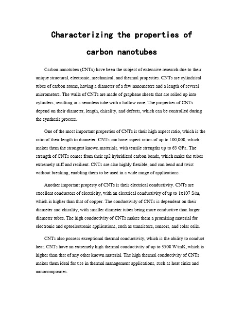
Characterizing the properties ofcarbon nanotubesCarbon nanotubes (CNTs) have been the subject of extensive research due to their unique structural, electronic, mechanical, and thermal properties. CNTs are cylindrical tubes of carbon atoms, having a diameter of a few nanometers and a length of several micrometers. The walls of CNTs are made of graphene sheets that are rolled up into cylinders, resulting in a seamless tube with a hollow core. The properties of CNTs depend on their diameter, length, chirality, and defects, which can be controlled during the synthesis process.One of the most important properties of CNTs is their high aspect ratio, which is the ratio of their length to diameter. CNTs can have aspect ratios of up to 100,000, which makes them the strongest known materials, with tensile strengths up to 63 GPa. The strength of CNTs comes from their sp2 hybridized carbon bonds, which make the tubes extremely stiff and resilient. CNTs are also highly flexible, and can bend and twist without breaking, enabling them to be used in a wide range of applications.Another important property of CNTs is their electrical conductivity. CNTs are excellent conductors of electricity, with an electrical conductivity of up to 1x10⁷ S/m, which is higher than that of copper. The conductivity of CNTs is dependent on their diameter and chirality, with smaller diameter tubes being more conductive than larger diameter tubes. The high conductivity of CNTs makes them a promising material for electronic and optoelectronic applications, such as transistors, sensors, and solar cells.CNTs also possess exceptional thermal conductivity, which is the ability to conduct heat. CNTs have an extremely high thermal conductivity of up to 3500 W/mK, which is higher than that of any other known material. The high thermal conductivity of CNTs makes them ideal for use in thermal management applications, such as heat sinks and nanocomposites.Furthermore, CNTs are highly hydrophobic, meaning that they repel water. This property makes them useful in applications where water resistance is required, such as in coatings and membranes. CNTs are also resistant to chemical corrosion and oxidation, which makes them highly durable and long-lasting.However, CNTs also have some limitations that need to be addressed. One of the major challenges is their toxicity. While CNTs have shown great promise in medical applications, such as drug delivery and cancer therapy, their potential toxicity to cells and tissues is a cause of concern. Studies have shown that CNTs can cause lung damage and inflammation in rodents, raising questions about their safety for human use. Therefore, it is important to thoroughly evaluate the toxicity of CNTs before using them in biomedical applications.In conclusion, CNTs are a remarkable material with unique and exceptional properties that make them suitable for a wide range of applications. Their high strength, electrical and thermal conductivity, hydrophobicity, and chemical stability make them a promising material in the fields of electronics, energy, and healthcare. However, their potential toxicity needs to be addressed before they can be widely used in biomedical applications. Understanding the properties of CNTs is essential for developing new applications that can exploit their exceptional properties while minimizing their drawbacks.。
氧化铋

Structural and multiferroic properties of La-modified Bi Fe O 3 ceramicsS. R. Das, R. N. P. Choudhary, P. Bhattacharya, R. S. Katiyar, P. Dutta, A. Manivannan, and M. S. SeehraCitation: Journal of Applied Physics 101, 034104 (2007); doi: 10.1063/1.2432869View online: /10.1063/1.2432869View Table of Contents: /content/aip/journal/jap/101/3?ver=pdfcovPublished by the AIP PublishingArticles you may be interested inEffect of Pr- and Nd- doping on structural, dielectric, and magnetic properties of multiferroicBi0.8La0.2Fe0.9Mn0.1O3J. Appl. Phys. 115, 134102 (2014); 10.1063/1.4870454Improved dielectric and magnetic properties of Ti modified BiCaFeO3 multiferroic ceramicsJ. Appl. Phys. 113, 023908 (2013); 10.1063/1.4774283Structural, magnetic, and optical properties of Pr and Zr codoped BiFeO3 multiferroic ceramicsJ. Appl. Phys. 112, 094102 (2012); 10.1063/1.4761968Structure and properties of La-modified Na0.5Bi0.5TiO3 at ambient and elevated temperaturesJ. Appl. Phys. 112, 054111 (2012); 10.1063/1.4751357Structural and physical properties of room temperature stable multiferroic properties of single-phase ( Bi 0.9 La 0.1 ) FeO 3 – Pb ( Fe 0.5 Nb 0.5 ) O 3 solid solution systemsJ. Appl. Phys. 105, 07D919 (2009); 10.1063/1.3072034Structural and multiferroic properties of La-modified BiFeO3ceramics S.R.Das,R.N.P.Choudhary,P.Bhattacharya,and R.S.Katiyar a͒Department of Physics,University of Puerto Rico,San Juan,PR-00931,Puerto RicoP.Dutta,A.Manivannan,and M.S.SeehraDepartment of Physics,West Virginia University,Morgantown,West Virginia26506͑Received4May2006;accepted23November2006;published online6February2007͒The coexistence of the magnetic and the electrical properties in lanthanum͑La͒-modified bismuthferrite͑Bi1−x La x FeO3,x=0.05,0.1,0.15,and0.2͒ceramics was studied and compared with those ofbismuth ferrite͑BiFeO3͒.The presence of a small secondary phase of BiFeO3͑arises due to excessBi2O3͒was removed on La substitution at the Bi site,as observed in x-ray diffraction͑XRD͒.Theeffect of La substitution on dielectric constant,loss tangent,and remnant polarization of the sampleswas studied in a wide range of temperature͑77–400K͒and frequency͑1kHz–1MHz͒.Thevariation of magnetization,coercivefield,and exchange bias with temperature͑2–300K͒and Laconcentration were investigated.These changes in the magnetic parameters with La doping alongwith those of the electron magnetic resonance parameters measured at300K and9.28GHz areunderstood in terms of increase in the magnetic anisotropy and magnetization.These results alsoshow that stabilization of crystal structure and nonuniformity in spin cycloid structure by Lasubstitution enhances the multiferroic properties of BiFeO3.©2007American Institute of Physics.͓DOI:10.1063/1.2432869͔I.INTRODUCTIONBismuth ferrite͑BiFeO3͒has recently gained consider-able importance both technologically and scientifically be-cause of the existence of both ferroelectrics and͑anti͒ferro-magnetic ordering in the same phase in the material,and also magnetoelectric coupling between the two respective order parameters͑spin and charge͒.Unfortunately,spontaneous polarization and magnetization of the material at room tem-perature are small due to large leakage current and loss tan-gent,and hence it is difficult to study the dielectric properties in the low frequency range.1,2Therefore,Krainik et al.3mea-sured the temperature dependence of dielectric constant of bismuth ferrite͑BFO͒at microwave frequencies.The low value of polarization is attributed to the presence of second-ary phases and low resistivity of BiFeO3ceramics whereas the high leakage current is attributed to the presence of Fe2+ ions.4,5In order to increase the dielectric constant,reduce the leakage current,and hence to improve the ferroelectric po-larization in BFO,some attempts have been made including a small doping at the Bi/Fe sites.There are also several reports on the synthesis of solid solution of BiFeO3with other perovskite structures͑with different concentrations͒, which has improved electrical properties of BFO.Fedulov et al.6studied the BiFeO3–PbTiO3solid solutions,and re-ported that up to78mole%of BiFeO3the structure remains rhombohedral,after which it becomes tetragonal.Ismailzade et al.7showed that in BiFeO3–BaTiO3solid solution,the structure remains rhombohedral for67mole%of BiFeO3, from67toϳ6mole%it is cubic,and below6mole%,the structure of solid solution transforms to tetragonal.There are also some reports on the ferroelectric and ferromagnetic properties of cationic substituted BiFeO3.8–10Palkar et al.9,10 reported the ferroelectric and ferromagnetic properties of La and Tb at the Bi site,and La at the Bi site and Mn at the Fe site substituted BiFeO3.Though they did not observed any improvement in the ferroelectric properties in La/Mn-substituted BiFeO3,a small enhancement of mag-netic properties was clearly observed.The͑La,Tb͒substi-tuted at the Bi site in BiFeO3ceramic showed high values of dielectric constant and magnetoelectric coupling at room temperature.Recently,Wang et al.8observed an improve-ment in the dielectric properties of BiFeO3on substituting La at the Bi site and Ga at the Fe site,and making its composite with43mole%of PbTiO3.The room temperature dielectric constant was found to be1800with low loss tangent of0.024,and T c shifted toϳ500from1103K͑BiFeO3͒.Also,a larger induced magnetization͑compared to single crystal BiFeO3͒was obtained at room temperature at much lower magneticfield,and the magnetization value increased at5K.BiFeO3has a ferroelectric Curie temperature T c Ϸ1103K and antiferromagnetic͑AF͒Neel temperature T N Ϸ643K.11Since T c and T N are significantly different,it may be argued that spin and polarization ordering must be un-coupled and driven by different modes.The AF ordering is not completely compensated because of observed weak magnetism.12Neutron diffraction studies13have shown an incommensurately modulated cycloidal spin structure with a long wavelengthϷ600Å.In electron magnetic resonance ͑EMR͒studies,a low-field mode with paramagnetic-resonance-like linear relationship between energy andfield ͑h=gB H͒is observed for TϽT N with gϷ2.0͑for low La concentration͒,in addition to the highfield antiferromagnetic resonance͑AFMR͒modes,with criticalfield͑spinflip͒Ϸ18kOe.11In thinfilms of BiFeO3,the enhanced polariza-tion and magnetization have been interpreted due to epitaxiala͒Author to whom correspondence should be addressed;FAX:ϩ1-787-764-2571;electronic mail:rkatiyar@JOURNAL OF APPLIED PHYSICS101,034104͑2007͒0021-8979/2007/101͑3͒/034104/7/$23.00©2007American Institute of Physics101,034104-1constraint destroying the cycloidal ordering.14,15Magneto-electric properties of epitaxially grown La-modified BiFeO 3thin films have recently been reported by Lee et al.16and showed enhancement in the polarization and magnetization.In this paper,we report the effect of La substitution ͑5–20mole %at the Bi site ͒on structural,electrical,and magnetic properties of BiFeO 3ceramics ͓i.e.,Bi 1−x La x FeO 3͑BFOL ͔͒.II.EXPERIMENTThe high purity ͑99.9%,Alfa Aesar ͒bismuth oxide ͑Bi 2O 3͒,iron oxide ͑Fe 2O 3͒,and lanthanum oxide ͑La 2O 3͒were mixed ͑stoichiometry ͒in an agate mortar and pestle in wet medium ͑alcohol ͒to prepare BiFeO 3͑BFO ͒and Bi 1−x La x FeO 3͓x =0.05͑BFOL5͒,x =0.10͑BFOL10͒,x =0.15͑BFOL15͒,and x =0.20͑BFOL20͔͒ceramics.The slurries of the above mixtures were dried overnight in anoven at 50°C.The homogeneous mixed powders were cal-cined at different temperatures for different duration.BFO powder was calcined in two different steps;͑a ͒500°C.for 1h and ͑b ͒850°C.for 2h.The calcination temperatures/time for BFOL5/BFOL10and BFOL15/BFOL20were found to be 870°C/2h and 890°C/2h,respectively.The fine calcined powders of BFO and BFOL were used to make circular pellets of 7mm diameter and 1–2mm thickness.All the pellets were sintered at 890°C.for 4h for densifi-cation.In order to study phase formation and to carry out pre-liminary structural analysis of BFO and BFOL,x-ray diffrac-tion pattern were taken using Cu K ␣radiation ͑=1.5405Å͒of a Seimens D5000powder diffractometer.Dif-ferential thermal analysis of all the samples were carried out to study the phase transition behavior,using Shimatzu differ-ential thermal analyses ͑DTA ͒thermal analyser.The scan-ning electron micrographs ͑SEM ͒of the pellet samples were taken to study the grain size and size distributions.The di-electric constant and loss tangent were measured using an impedance analyzer ͑HP4294A ͒and temperature controller ͑M/s MMR Technology,Inc.͒in a wide range of frequencies ͑1kHz–1MHz ͒and temperatures ͑77–500K ͒.Ferroelec-tric polarizations were measured on poled samples using a hysteresis loop tracer ͑M/s Radiant Technology Inc.͒.The magnetization M as a function of applied field H at different temperatures ͑2–300K ͒was measured using a supercon-ducting quantum interference device ͑SQUID ͒magnetome-ter.The EMR studies of all the samples were carried out at 300K using an X -band spectrometer operating at 9.28GHz.TABLE parison of lattice parameters,and tolerance factors of ͑Bi 1−x La x ͒FeO 3ceramics.The estimated standard deviations are in the positiona ͑Å͒c ͑Å͒V ͑Å͒3t x =0.0 5.6206͑20͒13.6924͑20͒374.570.915x =0.05 5.6011͑80͒13.6472͑80͒371.010.916x =0.10 5.6019͑70͒13.6429͑70͒370.770.917x =0.15 5.5942͑48͒13.6386͑48͒369.640.919x =0.205.5879͑48͒13.6066͑48͒367.940.920FIG.1.X-ray diffraction patterns of BiFeO 3and Bi 1−x La x FeO 3͑0.05ഛx ഛ0.2͒polycrystalline ceramics.FIG.2.Differential thermal analyses ͑DTA ͒of BiFeO 3and Bi 1−x La x FeO 3͑0.05ഛx ഛ0.2͒.FIG.3.Scanning electron micrographs ͑SEM ͒of BFO,BFOL5,BFOL10,and BFOL20ceramics.III.RESULTS AND DISCUSSIONFigure 1shows the XRD pattern of BFO and BFOL ceramics.All the diffraction peaks of BFO were indexed and lattice parameters were determined in a hexagonal unit cell using a powder diffraction refinement computer program.17The La-modified BiFeO 3was also fitted with the same crys-tal structure.Though all the diffraction peaks were well iden-tified,few low intensity peaks were observed at 2ϳ27°–28°in case of BiFeO 3ceramic.Upon La substitution at the Bi site,the impurity phase was eliminated.The impu-rity peaks were identified,probably because of the addition of 10%extra Bi 2O 3.Peak shifts were calculated using peak fit software.Table I compares the refined least squares lattice constants of BFO and BFOL with their estimated standard deviations in parenthesis.Figure 2shows the thermograms of BFO and BFOL powders in the temperature range of 0–1200°C.Three dis-tinct features were observed ͑based on change of slopes of all the curves ͒:͑a ͒ϳ300–350°C corresponds to Neel tempera-tures of magnetic phase transition,͑b ͒800–900°C corre-sponds to the ferroelectrics Curie temperatures/phase transi-tion,and ͑c ͒950–1150°C corresponds to the heat loss at the melting points of BFO and BFOL ceramics.These observa-tions suggest that the lanthanum substitution lowered the ferroelectric phase transition temperature but increases the melting point of BFO.Figure 3shows the scanning electron micrographs of BFO and BFOL ceramics.The average grain size of all the samples is very much similar,and in the range of 2–3m.However,it can be noticed that with a small lanthanum con-centration ͑5–10mole %͒,the density of sample ͑i.e.,lessvoids ͒increases.In the BFOL20sample,small grains coa-lesce to form large grains,and hence different microstruc-tures of large grain size are obtained.The microstructures and absence of secondary phases on La substitution in BFO are some of the main reasons for enhanced electrical and magnetic properties of BFOL.Figures 4͑a ͒and 4͑b ͒show the variation of dielectric constant of BFOL with frequency at 300and 630K,respec-tively.It is observed that at higher temperature ͑630K ͒,the dielectric constant of the ceramic samples increases by an order of magnitude ͑with minimal changes in BFOL10and BFOL15͒.This increase is considered as due to the magnetic phase transition around that temperature.This is more evi-dent from the Fig.5.At 300K,no frequency dispersion was observed in the material ͑with an exception of BFOL5͒.However,at 630K most of the ceramic samples exhibited frequency dispersion at lower frequencies.Figures 5͑a ͒and 5͑b ͒show the temperature variation of dielectric constant at two different frequencies 100kHz and 1MHz,respectively.Because of temperature limitation of our sample holder ͑i.e.,maximum temperature=700K ͒,we could not obtain ferroelectric phase transition temperature of BFO and BFOL ͑as observed from DTA results ͒.However,a sharp increase in dielectric constant started from 500K for all the ceramics.Figures 6͑a ͒and 6͑b ͒show variation of loss tangent with temperature at 100kHz and 1MHz,respectively.At the lower frequency,the loss tangent is higher,and it decreases as a function of the frequency ͑lower frequency data are not shown here ͒.Around room temperature ͑ϳ300K ͒loss tan-gent peaks were observed for all the samples.AsevidentFIG.4.͓͑a ͒and ͑b ͔͒.Dielectric con-stant vs frequency ͑100kHz–1MHz ͒of BFO and BFOL ceramics at 300and 630K.FIG.5.͓͑a ͒and ͑b ͔͒.Dielectric con-stant vs temperature of BFO and BFOL ceramics at 100kHz and 1MHz.from our dielectric measurements,dielectric anomaly of BFOL corresponds to the magnetic phase transition tempera-tures.Both the dielectric constant and the loss tangent of all the ceramics have a signature of attaining local maxima,a characteristic for multiferroics.Figure 7shows the ferroelectric hysteresis loops mea-sured on poled samples of BFO,BFOL5,and BFOL20at 300K and at different applied fields.BFO did not give a perfect ferroelectric loop.However,on La substitution,the loop gradually changes to that of ferroelectric nature reduc-ing the leakage.Still the samples are not totally leakage free.The ferroelectric polarization of x =0.05sample,which has a better microstructure and higher dielectric constant is shown for comparison.The remnant polarization of BFOL20ce-ramic was found to be 2P r Ϸ13C/cm 2at an applied field of 20kV/cm.These suggest the improvement of electrical and ferroelectric properties upon lanthanum substitutions at the Bi site in BFO ceramics.Figure 8shows the magnetization M versus applied field H of BFO and BFOL at room temperature ͑BFOL5data not shown in the figure ͒.Asymmetric hysteresis loops at 300and2K were obtained from which we measured the coercivity H c ,the exchange bias H e ,the average remanence magnetiza-tion M r =͑M r ++M r −͒/2and the magnetization at 55kOe ͑de-fined as M H ͒.In Table II ,we have compared the value of these quantities for all the BFO and BFOL samples.All the samples have negative H e ͑i.e.,their loops are shifted to the negative side by exchange bias ͒.At T =2K the magnitudes of the loop parameters ͑H c ,H e ,M H ,and M r ͒increase on increasing La concentration.The enhancement of the mag-netic parameters,perhaps due to increased magnetoelectric coupling 8,18on La-modified BFO are observed here.The hysteresis loops parameters ͑at 300K ͒for the samples of BFO ͑Table II ͒are presented graphically in Fig.8͑inset ͒.The M vs H curves are nearly linear,and hence M does not have any tendency to saturate even at 55kOe.Consequently the saturation magnetization cannot be determined and only the magnetization at 55kOe,viz.,M H is listed in Table II .For 20%La in BFO,a typical loop in the low field region was observed.Similar sets of data were obtained at 2K,except the magnitudes of H e ,H c ,and M H aredifferent.FIG.6.͓͑a ͒and ͑b ͔͒.Loss tangent vs temperature of BFO and BFOL ceram-ics at 100kHz and 1MHz.FIG.7.Ferroelectric hysteresis of BFO,BFOL5,and BFOL20ceramics at different applied fields.In Fig.9͑a ͒,we plot the magnitude of the negative ex-change bias,viz.,H e of BFOL both at T =2and 300K.A similar plot for the coercivity H c and the average remanence M r is shown in Figs.9͑b ͒and 9͑c ͒,respectively,where a systematic increase in their magnitudes with La doping is observed,especially at 2K.We also measured temperature dependence of H c ,H e ,and M H ͑Fig.10͒of BFO,where H c increases with increase in temperature and H e goes through a maximum near 100K.The presence of exchange bias H e in all our samples here is most intriguing since H e usually signifies the presence of a ferromagnet/antiferromagnet ͑F/AF ͒interface in a system.19–21In the weak ferromagnet ␣-Fe 2O 3,in which Dzyloshisky-Moriya ͑DM ͒antisymmetric exchange interac-tion is considered as the source of weak ferromagnetism,we did not observe exchange bias in a separate experiment not reported here.In BFO,the conventional DM interaction is zero.11A magnetoelectric interaction ͑such as DM interac-tion ͒,which couples both to the polarization and magnetiza-tion,has been introduced to explain the cycloidal spin struc-ture and its transformation to a homogeneous AF state under an applied magnetic field.11–16,18–22Whether the observed ex-change bias can be theoretically explained by this DM inter-action still needs to be understood.The temperature dependence of the low-field ͑H =200Oe ͒susceptibility for all the samples is shown in Fig.11.The temperature dependence of is quite subtle except for the pure BFO sample,which obeys Curie law at lower temperatures,perhaps due to an otherwise undetected para-magnetic impurity.Also,in the 20%La doped sample,is considerably lower which may be due to the different shape of its hysteresis loop ͑Fig.8͒.Figure 12shows the room temperature EMR studies of all the samples at 9.28GHz suggesting an EMR line near g Ϸ2.0for BFO,BFOL5,and BFOL10samples,which is in good agreement with the observations of Ruette et al.11The samples with 15%and 20%La doping have higher gvalues.FIG.8.Magnetic hysteresis loops of BFO and BFOL samples.The insets show the details of the loops for lower fields.TABLE II.Magnetic parameters of ͑Bi x La x ͒FeO 3͑x =0.0,0.05,0.10,0.15,and 0.20͒at room temperature.Composition H c ͑Oe ͒H e ͑Oe ͒M r ͑emu/g ͒M H ͑emu/g ͒at 55kOe⌬H ͑Oe ͒g value ͑⌬H ͒2ᐉ͑104͒/mg x =0620−3500.00380.35335 2.04 3.16x =0.05478−1800.00320.35900 2.0314.3x =0.101045−3600.00770.401050 2.0517.5x =0.152840−3250.02150.401480 2.1655.4x =0.20840−3300.07360.5518602.52304The peak-to-peak linewidth ⌬H and the line intensity I =͑⌬H ͒2ᐉ͑ᐉ=peak-to-peak height ͒of this line also increase with increase in La doping.These observed changes in the EMR and magnetic parameters with increase in La doping ͑Table II ͒are mutually consistent in the following way.The increase in H c implies increase in magnetic anisotropy,which in turn increases the EMR linewidth ⌬H and gvalues.23Since the EMR line intensity is proportional to ͑⌬H ͒2as noted above,the line intensity also increases with increase in La doping.In the doped samples,a second over-lapping line begins to emerge and shifts to lower fields with increasing La doping.Since exchange bias H e is also ob-served in the undoped BFO,it is unlikely that the source of this line is related to the presence of the exchange bias.The EMR parameters ͑Table II ͒represent values for the compos-ite line observed here since it is difficult to completely re-solve the two lines.The second line could result from any nonuniformity in the spatial magnetization of the samples such as from magnetic domains.Because of the increase of the EMR linewidth and H c with increase in La doping,both signifying increase in anisotropy,domains are more likely to be present for the larger Ladopings.FIG.9.Effect of La doping on ͑a ͒exchange bias ͑−H e ͒,͑b ͒coercivity H c ,and ͑c ͒average magnetization M r at 2and 300K.Lines joining the points are for visualaid.FIG.10.Temperature dependence of exchange bias ͑−H e ͒,coercivity ͑H c ͒,and magnetization M H at 55kOe for the BFO.Lines joining the points are for visualclarity.FIG.11.Temperature dependence of the low-field susceptibility measured at H =200Oe for BFO and BFOLceramics.FIG.12.Room temperature EMR spectra of the BFO and BFOL samples measured at f =9.28GHz.The vertical line marks the calculated position for g =2.0.IV.CONCLUSIONSPure and La substituted BiFeO3ceramics were synthe-sized using solid-state reaction substitution at Bisite eliminated the small impurity phase of BiFeO3and sta-bilized the crystal structure into hexagonal symmetry.Though the dielectric properties were not enhanced by Lasubstitution,systematic increase in both the ferroelectric andferromagnetic properties were achieved.The observed in-creases in the magnetic parameters͑H c,H e,and M r͒and EMR parameters͑⌬H,g,intensity I͒with increase in Ladoping reflect corresponding increases in the magnetic aniso-tropy and magnetization.However,the observation of ex-change bias H e in this ferromagnetic-ferroelectric system ismost intriguing and requires theoretical interpretation.It ishoped that these studies will stimulate such an investigation. ACKNOWLEDGMENTThis research was supported in part by NSF͑DMR0305588͒and DOD͑W911NF-06-1-0030͒grants.1Yu.E.Roginskaya,Yu.Ya.Tomashpol’ski,Yu.N.Venevtsev,V.M. Petrov,and G.S.Zhdanov,Sov.Phys.JETP23,490͑1966͒.2I.R.Teague,R.Gerson,and W.J.James,Solid State Commun.8,1073͑1970͒.3N.N.Krainik,N.P.Khuchua,V.V.Zhdanova,and V.A.Evseev,Fiz. Tverd.Tela͑S.-Peterburg͒8,816͑1966͒.4S.T.Zhang,M.H.Lu,D.Wu,Y.F.Chen,and N.B.Ming,Appl.Phys. Lett.87,262907͑2005͒.5C.Ederer and N.A.Spaldin,Phys.Rev.B71,224103͑2005͒.6S.A.Fedulov,dyzhinskii,I.L.Pyatigorskaya,and Yu.N.Venevt-sev,Sov.Phys.Solid State6,375͑1964͒.7I.H.Ismailzade,R.M.Ismailov,A.I.Alekberov,and F.M.Salaev,Phys. Status Solidi A68,K81͑1981͒.8N.Wang,J.Cheng,A.Pyatakov,A.K.Zvezdin,J.F.Li,L.E.Cross,and D.Viehland,Phys.Rev.B72,104434͑2005͒.9V.R.Palkar,D.C.Kundaliya,and S.K.Malik,J.Appl.Phys.93,4337͑2003͒.10V.R.Palkar,D.C.Kundaliya,S.K.Malik,and S.Bhattacharya,Phys. Rev.B69,212102͑2004͒.11B.Ruette,S.Zvyagin,A.P.Pyatakov,A.Bush,J.F.Li,V.I.Belotelov,A. K.Zvezdin,and D.Viehland,Phys.Rev.B69,064114͑2004͒.12G.A.Smolenskii and I.Chupis,p.25,475͑1982͒.13I.Sosnowka,M.Loewenhaupt,W.I.F.David,and R.M.Ibberson, Physica B180–181,117͑1992͒.14F.Bai et al.,Appl.Phys.Lett.86,032511͑2005͒.15J.Li et al.,Appl.Phys.Lett.84,5261͑2004͒.16D.Lee,M.G.Kim,S.Ryu,H.M.Jang,and S.G.Lee,Appl.Phys.Lett. 86,222903͑2005͒.17E.Wu,computer code POWD,an interactive powder diffraction data inter-pretation and indexing program,Ver.2.1,School of Physical Sciences, Flinder University of South Australia,Bedford Park,SA5042,Australia. 18J.Hemberge,P.Lunkenheimer,R.Fichtl,H.-A.Knug V on Nidda,V.Tsur-kan,and A.Loidt,Nature͑London͒434,364͑2005͒.19W.H.Meiklejohn and C.P.Bean,Phys.Rev.102,1413͑1956͒;J.Appl. Phys.33,1328͑1962͒.20J.Nogues and I.K.Schullar,J.Magn.Magn.Mater.192,203͑1999͒. 21A.Punnoose,E.H.Morales,Y.Wang,D.Lederman,and M.S.Seehra,J. Appl.Phys.93,771͑2003͒.22I.Sosnowska and A.Zvezdin,J.Magn.Magn.Mater.140–144,167͑1995͒.23T.G.Castner and M.S.Seehra,Phys.Rev.B4,38͑1971͒.。
英汉互译

一、英译汉
Title: Aerogels with 3D Ordered Nanofiber Skeletons of
Liquid-Crystalline Nanocellulose Derivatives as Tough and Transparent Insulators
Abstract:
Aerogels of high porosity and with a large internal surface area exhibit outstanding performances as thermal, acoustic, or electrical insulators【1】. However, most aerogels are mechanically brittle and optically opaque, and the structural and physical properties of aerogels strongly depend on their densities. The unfavorable characteristics of aerogels are intrinsic to their skeletal structures consisting of randomly interconnected spherical nanoparticles【2】. A structurally new type of aerogel with a three-dimensionally ordered nanofiber skeleton of liquidcrystalline nanocellulose (LC-NCell) is now reported. This LCNCell material is composed of mechanically strong, surfacecarboxylated cellulose nanofibers dispersed in a nematic LC order. The LC-NCell aerogels are transparent and combine mechanical toughness and good insulation properties. These properties of the LC-NCell aerogels could also be readily controlled.
工艺参数对CrNx涂层性能的影响

工艺参数对CrNx涂层性能的影响宋慧瑾;鄢强;李玫;董志红;冯威;朱晓东;孙艳【摘要】采用直流磁控溅射技术制备了氮化铬(CrNx)涂层,研究了制备CrNx涂层的工艺参数对所制备的CrNx涂层的膜基结合力及力学性能的影响.研究结果表明:工艺参数对CrNx涂层性能的影响不成各向同性关系;在较低的N2含量、较高的脉冲偏压、约100V的直流偏压、较高的真空度、较高的沉积温度和较高的靶功率下制备的CrNx涂层的硬度较高,而在较低的N2含量、恰当的脉冲偏压和占空比配对、较高的直流偏压、较高的真空度、较高的沉积温度和较高的靶功率下制备的CrNx涂层的表面形貌较好.【期刊名称】《高技术通讯》【年(卷),期】2015(025)003【总页数】7页(P300-306)【关键词】氮化铬(CrNx);涂层;工艺参数;直流磁控溅射【作者】宋慧瑾;鄢强;李玫;董志红;冯威;朱晓东;孙艳【作者单位】成都大学工业制造学院成都610106;成都大学工业制造学院成都610106;西南石油大学机电工程学院成都610500;成都大学城乡建设学院成都610106;成都大学工业制造学院成都610106;成都大学工业制造学院成都610106;成都大学工业制造学院成都610106;成都大学工业制造学院成都610106【正文语种】中文氮化铬(CrNx)涂层硬度高、耐磨性好、摩擦系数低,具有高温抗氧化性和耐腐蚀性能,并且对有色金属及其合金化学惰性好,是加工铝合金、黄铜和镍合金等的理想涂层材料。
氮化铬涂层已经广泛应用在很多领域,近年来越来越受到人们的关注和重视[1-4]。
在机械制造和加工领域,氮化铬涂层的硬度较高,摩擦系数较低,与钢摩擦时,摩擦系数比钢-钢摩擦小20%~30%,比氮化钛-钢摩擦小10%~20%,因为使用中表面容易形成一层稳定致密、硬度高并且结合紧密的氧化层,所以氮化铬涂层作为耐磨涂层已广泛用于一些机械零部件、模具和切削工具的表面强化以增长使用寿命。
万青个人简历

6. C. C. Li, Z. F. Du, L. M. Li, H. C. Yu, Q. Wan, and T. H. Wang, "Surface-depletion controlled gas sensing of ZnO nanorods grown at room temperature", Applied Physics Letters. 91, 032101 (2007).
19. Q.Wan, K.Yu, T.H.Wang, C.L.Lin, "Low-field electron emission from tetrapod-like ZnO nanostructures synthesized by rapid evaporation", Applied Physics Letters, 83, 2253 (2003).
21. Q.Wan, T.H.Wang M.Zhu,and C.L.Lin,"Resonant tunneling of Si nanocrystals embedded in Al2O3 matrix prepared by electron-beam co-evaporation",Applied Physics Letters, 81, 538 (2002)
在研课题
2007年,湖南省杰出青年基金项目,负责人(30万)
国外期刊英文论文
Influence of Deformation
Li CL, Chen Mater. Sci. & 2002, 325: SCI a
14 Temperature on Shape Memory
DJ, Jin ZH Eng. A
375-379
EI
Effect of Fe-Mn-Si-Cr-Ni Alloy
Wang TJ
Comparison between fatigue
Qiao GJ,
Int. J. Fatigue 2002, 24(5): SCI a
17
behavior of some ceramics: a new concept of intrinsic stress-corrosion
Wang HJ, Jin ZH
Ding HF, Jin
258-264
EI
ZH
The interfacial stability of the
Tang WM,
Mater. Chem. 2002, 77:
SCI a
21 coated-SiC/Fe couple
Zheng ZX,
Phys.
Ding HF, Jin
236-241
EI
ZH
31
Unlubricated wear of Si/SiC and its composite with nickel Si/SiC-Ni
Sang KZ, Jin ZH
Tribology Int.
2001, 34(5): SCI a
315 -319
EI
Effects of crystalline morphology Xu T, Yu J, Jin Mater.
Influence_of_Composite_Non_Magnetic_Ions_(Cd-Ti)_D
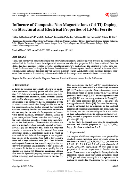
New Journal of Glass and Ceramics, 2012, 2, 144-149doi:10.4236/njgc.2012.24021 Published Online October 2012 (/journal/njgc)Influence of Composite Non Magnetic Ions (Cd-Ti) Doping on Structural and Electrical Properties of Li-Mn Ferrite Vidya J. Deshmukh1, Pragati S. Jadhav2, Ketaki K. Patankar2*, Sharad S. Suryawanshi3, Vijaya R. Puri4 1Ramkrishna Paramhansa Mahavidyalaya, Osmanabad College, Osmanabad, India; 2Physics Department Rajaram College, Kolhapur, India; 3Physics Department, Solapur University, Solapur, India; 4Physics Department, Shivaji University, Kolhapur, India.Email: *Received May 6th, 2012; revised July 23rd, 2012; accepted August 16th, 2012ABSTRACTThe Li-Mn ferrites with composite divalent and tetravalent non-magnetic ions doping were prepared by ceramic method and studied for the first time to investigate their structural and electrical properties. It has been confirmed from the studies that these materials result in properties suitable for microwave applications. The structural properties have con- firmed the formation of cubic spinel ferrite and the substitutions of non magnetic ions have resulted in increase of unit cell dimensions and hence the grain size with increase in dopant content. An IR study asserts the same. Electrical Prop- erties show increase in dc resistivity and decrease in dielectric loss tangent with increase in dopant concentration. Keywords: Electronic Materials; Magnetic Ceramics; Electrical Characterization; Powder Diffraction1. IntroductionLi ferrite is becoming increasingly attractive for micro- wave applications replacing garnets and other spinel fer- rites [1-3]. Microwave devices such as circulators, isola- tors, magnetostatic resonators, filters, switches, limiters and tunable electroptic modulators are the microwave applications of Li ferrites [4]. Recent exponential growth in microwave communication through mobile and satel- lite communications has further stressed the worldwide need for extremely low-loss and economical microwave devices using ferrite materials. In preparation of micro- wave ferrite materials, particular attention should be given to the purity of the raw materials, stoichiometry of the composition and porosity as well as grain characteris- tics of the final product. Characteristics of various mi- crowave ferrites have been minutely reported by Voron- kov et al. [5]. The emergence of Li ferrite as a competent material in microwave devices has resulted from some appropriate chemical substitutions made in it, which in turn result in low dielectric loss tangent, a low magnetic loss tangent at the operating bias field, a low coercive force and a large remanence ratio [6-8]. Low dielectric and magnetic losses are the essential requisites for mi- crowave applications Small amounts of Mn3+ is added to microwave Li ferrites to ensure an acceptably low di- electric loss tangent [9]. Moreover, manganese addition also alter the hysteresis property, reduces magnetocrys- talline anisotropy and magnetostriction in ferrites [9]. Non magnetic ions like Cd2+ and Ti4+ substitutions have been found to be most suitable to obtain high resistivity [10,11]. The site occupancies of the various cations known from earlier works are given as follows. Li1+ has strong preference for B-Site [12], Cd2+ has strong preference for A site [1], Ti4+ also has strong preference for B-site [13], Fe2+ has strong preference for B-site [1] and Mn3+ has strong preference for B-site [14]. From the above survey, it can be envisaged that investigations on the electrical properties of composite non-magnetic ions doping in Li-Mn ferrite may lead to more interesting results as the studies on their independent doping in Lithium ferrites have al- ready resulted in properties suitable for microwave ap- plications [10,11].In this view, the present paper aims to communicate structural and electric properties in Li0.35Cd x Ti x Mn0.1 Fe2.55–2x O4 where x varies from 0 to 0.5.2. ExperimentalSix samples of different compositions were prepared by standard ceramic technique using pure metal oxides in the form of a series Li0.35Cd x Ti x Mn0.1Fe2.55–2x O4 with x = 0.0, 0.1, 0.2, 0.3, 0.4 and 0.5. AR grade chemicals of Li2CO3, CdO, TiO2, Mn2O3 and Fe2O3 were used for the preparation of various compositions in the above ferrite series. These oxides were weighed in the required mole proportions using a single pan balance having least count 0.001 gm and mixed thoroughly in the agate-mortar in acetone for about 2 hrs. The mixture was sieved using a*Corresponding author.Influence of Composite Non Magnetic Ions (Cd-Ti) Doping on Structural and Electrical Properties of Li-Mn Ferrite 145sieve of mesh size 200 micron. The mixture of each com- position was preheated in platinum crucible and were presintered at 300˚C for 2 hours and followed by 600 Influence of Composite Non Magnetic ions (Cd-Ti) Do- ping on Structural and Electrical Properties of Li-Mn Ferrite for 4 hrs and finally sintered at 1000˚C for 8 hours.X-ray Diffractograms of various compositions were obtained using X ray diffractometer Model PW 3710. The various parameters used for X ray diffraction were Target—Cu Kα; Wavelengths λ1 = 1.54056 Å and λ2 = 1.54439 Å; Rate of Scanning—2˚/min and scanning an-gle range 2θ—20˚ to 90˚. Micrographs of various sam- ples were obtained using the scanning electron micro- scope SEM (model JSM-6360A). IR absorption peaks of various compositions were studied using PerkinElmer IR spectrometer (Model 783) with KBr as a solvent. DC resistivities of various prepared samples were studied using two probe set up. Dielectric constant and loss tan- gent in the frequency range 100 Hz - 1 MHz were also measured using HP LCR meter 4284A model.3. Results and DiscussionThe X-Ray diffraction patterns for Li0.35Cd x Ti x Mn0.1 Fe2.55–2x O4 system show sharp peaks indicating formation of single phase spinel ferrite for all compositions. How- ever trace amount of α-Fe2O3 phase is found for x = 0.3 sample. Hence the XRD of x = 0.3 composition is given in the Figure 1. The α-Fe2O3 phase is formed because at higher sintering temperature (>500˚C) there is possibil- ity for a fraction of ferric oxide to get converted into α-Fe2O3. The presence of such a phase in different ferrite is already reported by earlier workers [15].The lattice parameter increases with increasing the content of Cd2+and Ti4+ ions and is shown in Figure 2. This is in accordance with Vegard’s law. The Cd2+ ions have larger ionic radius (0.97 Å) as compared to Fe3+Figure 1. Fe2O3 pattern XRD of Li0.35Cd0.3Ti0.3Mn0.1 Fe1.95O4.Figure 2. Variation of lattice parameter with Cd and Ti content [x] in Li0.35 Cd x Ti x Mn0.1Fe2.55–2x O4 series.(0.65 Å), Ni2+ (0.74 Å) and Li1+ (0.71 Å) ions. The Cd2+ ions successively replace Fe3+ ions on A-site this results in an increase of lattice parameter with Cd content. Same is true for Ti ions at B-sites. Similar results were ob- tained when Cd and Ti were separately doped in Li fer- rite [10,11]. The compositional variations however sug- gest that the lattice parameters for composite non-mag- netic ions doping is increased to larger extent in com- parison to their separate doping in ferrites.The SEM technique was studied to understand the surface morphology of the samples. All compositions have grains with sharp boundaries indicating that grains are fully developed, well packed, crack free with clear grain boundaries. The grain boundaries are district and grains are closely packed in some cases which suggest that compositions exhibit high density values. The SEM images denoted by a, b, c, d, e, and f shows micrographs for compositions x = 0.0, 0.1, 0.2, 0.3, 0.4, and 0.5. With the addition of Cd-Ti ions the average grain size in- creases as shown in the Figures3(a)-(f). The increase in grain diameter with Cd and Ti content is attributed to the smaller solid solubility of lithium in the samples. It is obvious from the generic formula.The IR spectra of one representative member of ferrite series i.e. x = 0.3 is shown in Figure 4. The IR absorp- tion bands were observed in the range 600 cm–1 to 400 cm–1. The absorption bands obtained in the present investi- gation are found to be in the range reported for many other lithium containing ferrites [16,17]. The difference in band position ν1 and ν2 is expected because the Fe3+-O2–distance for B site (0.199 nm) is different from that of A site (0.189 nm). The tetrahedral vibrations are of bond stretching type while octahedral vibrations are of bond bending type. These types of vibrations also affect the absorption frequency. The octrahedral complex band is found to be suppressed with increase in composite non- magnetic ions content in the ferrite. This can be attri- buted to increase in the lattice parameter and average grain size with increase in Cd-Ti content.Influence of Composite Non Magnetic Ions (Cd-Ti) Doping on Structural and Electrical Properties of Li-Mn Ferrite 146(a) (b) (c)c(d) (e) (f)Figure 3. SEM of series Li0.35Cd x Ti x Mn0.1Fe2.55–2x O4 with x = 0 to 0.5.Variation of logρ vs 103/T for the samples Li0.5Cd x Ti xMn0.1Fe2.55–2x O4 and Li0.35Cd x Ti x Mn0.1Fe2.55–2x O4 with x =0, 0.1, 0.2, 0.3, 0.4, and 0.5 are shown in Figure 5. Allthe plots exhibit a linear relationship suggesting that theresistivity obeys a relation ρ =ρ0 exp(ΔE/kT) and cha-nge in slope is observed in case of all the compositions.From figure, it is seen that the variation is almost linearup to Curie temperature where a break occurs indicatinga change of magnetic ordering from ferrimagnetic to para-magnetic. The temperatures where breaks occur coincidewith the Curie temperature determined by permeabilitymeasurements which is not reported here. The exponen-tial increase in resistivity on decrease in temperature isdue to decrease in thermally activated mobility of thecharge carrier. The change in slope is attributed to thechange in the activation energy due to phase transition ofthe material from ferromagnetic to paramagnetic state.This anomaly strongly supports the influence of magneticordering upon the conductivity process in-ferrites. Manyworkers have studied logρ vs (1/T) and observed similarbehaviour suggesting that resistivity obeys the Arrheniusrelation [11,18]. Resistivity studies show that resistivity(ρdc) of the samples in the compositions increase as theCd2+, Ti4+ concentration increases similar to that reportedin 10 and 11 D.C. resistivity of Li-Cd-Ti ferrite can beexplained on the basis of a model based on phonon as-sisted electron hopping. Trace amount of Fe2+ ions arepresent in the present ferrites. The electrons are known toparticipate in the exchange process by the following re-action Fe2+↔ Fe3+ + e. Hence these electrons arestrongly coupled to the lattice and tunnel from one site tothe other due to phonon induced transfer mechanism.Ti4+ ions, being tetravalent, localize Fe2+ ions in the sys-tem and tunneling of electrons by transfer mechanism isretarded due to the reduction of Fe3+ ions which enhancesthe resistivity. The activation energy is estimated to be0.21 eV, which in turn confirms the conduction in pre-sent ferrites are due to small polarons [18].The dielectric constant decreases with increase in fre-quency showing dielectric dispersion as depicted in Fig-ure 6. The decrease in ε with frequency is natural be-cause of the fact that any species contributing to polar-izability is found to show lagging behind the appliedLi-Cd-Ti ferrite can be explained on the basis of a modelbased on phonon assisted electron hopping. Traceamountof Fe2+ ions is present in the present ferrites. The electronsare known to participate in the exchange process by thefollowing reaction Fe2+↔ Fe3+ + e. Hence these elec-trons are strongly coupled to the lattice and tunnel fromone site to the other due to phonon induced transfermechanism. Ti4+ ions, being tetravalent, localize Fe2+ions in the system & tunneling of electrons by transfermechanism is retarded due to the reduction of Fe3+ ionswhich enhances the resistivity. The activation energy isestimated to be 0.21 eV, which in turn confirms the con-duction in present ferrites are due to small polarons [18].Influence of Composite Non Magnetic Ions (Cd-Ti) Doping on Structural and Electrical Properties of Li-Mn Ferrite 1474. ConclusionThe Li 0.35Cd x Ti x Mn 0.1Fe 2.55–2x O 4 system has been suc- cessfully prepared with standard ceramic technique. The most intense (311) peak in XRD pattern confirms the formation of cubic spinel ferrite. The SEM micrograph shows the agglomerated grain structure with sharp grainboundaries due to high sintering temperature. The IR studies show the absorption bands which are in good agreement to the studied literature. The electrical proper- ties study shows the Li-ferrites are the n-type semicon- ductors. The dielectric constant shows usual dispersionbehaviour.Figure 4. IR spectra of Li 0.35Cd x Ti x Mn 0.1Fe 2.55–2x O 4 with x = 0.3.123456789101111.522.533.5Figure 5. Variation of log ρ vs 103/T for Li 0.35Cd x Ti x Mn 0.1Fe 2.55–2x O 4.14822.533.544.555.56Figure 6. Variation of dielectric constant Є vs logf for ferrite system Li 0.35Cd x Ti x Mn 0.1Fe 2.55–2x O 4.33.544.555.56Figure 7. The plot of dielectric loss tangent (tan δ) vs logf for ferrite system Li 0.35Cd x Ti x Mn 0.1Fe 2.55–2x O 4.5. AcknowledgementsAuthor K. K. Patankar is thankful to UGC, New Delhi for the financial assistance in the form of major research project extended to her.REFERENCES[1] R. G. Kharabe, R. S. Devan, C. M. Kanamadi and B. K.Chougule, “Dielectric Properties of Mixed Li-Ni-Cd Fer- rites,” Smart Materials and Structures , Vol. 15, No. 2, 2006, pp. 229-334. doi:10.1088/0964-1726/15/2/N02[2] S. R. Sawant, D. N. Bhosale, N. D. Chaudhari and P. P.Bakare, “Electric Properties of NiCuZn Ferrites Synthe- sized by Oxalate Precursor Method,” Journal of Materi- als Science , Vol. 3, 2002, pp. 617-622. [3] B. P. Ladgaonkar, P. N. Vasambekar and A. S. Vain-gankar, “Structural and DC Electrical Resistivity Study of Nd3+ Substituted Zn-Mg Ferrites,” Journal of Materials Science Letters , Vol. 19, No. 5, 2000, pp. 1375-1377. doi:10.1023/A:1006713518433 [4] M. Pardavi-Horvath, “Microwave Applications of SoftFerrites,” Journal of Magnetism and Magnetic Materials , Vol. 215-216, 2000, pp. 171-183.Influence of Composite Non Magnetic Ions (Cd-Ti) Doping on Structural and Electrical Properties of Li-Mn Ferrite 149doi:10.1016/S0304-8853(00)00106-2[5]V. Voronkov, “Microwave Ferrites: The Present and Fu-ture,” Journal of Physics IV (Paris), Vol. 7, No. 1, 1997, pp. 35-38.[6] D. Ravinder, “Dielectric Behaviour of Lithium-CadmiumFerrites,” Physica Status Solidi (A), Vol. 129, No. 2, 1992,pp. 549-554. doi:10.1002/pssa.2211290225[7]S. S. Bellad, S. C. Watawe and B. K. Chougule, “SomeAc Electrical Properties of Li-Mg Ferrites,” Materials Re- search Bulletin, Vol. 34, No. 7, 1999, pp. 1099-1106.doi:10.1016/S0025-5408(99)00107-5[8]V. P. Reddy and D. V. Reddy, “Far-Infrared Spectral Stu-dies of Some Lithium-Nickel Mixed Ferrites,” Journal ofMagnetism and Magnetic Materials, Vol. 136, No. 3, 1994,pp. 279-283. doi:10.1016/0304-8853(94)00321-1[9]P. P. Hankare, R. P. Patil, U. B. Sankpal, S. D. Jadhav, I.S. Mulla, K. M. Jadhav and B. K. Chougule, “Magnetic and Dielectric Properties of Nanophase Manganese-Sub- stituted Lithium Ferrite,” Journal of Magnetism and Mag-netic Materials, Vol. 321, No. 19, 2009, pp. 2977-3372.doi:10.1016/j.jmmm.2009.05.074[10]R. G. Kharabe, R. S. Devan and B. K. Chougale, “Struc-tural and Electrical Properties of Cd-Substituted Li-Ni Fer-rites,” Journal of Alloys and Compounds, Vol. 463, No.1-2, 2008, pp. 67-72.[11] D. Kothari, S. Phanjoubam and J. S. Baijal, “ElectricalConduction and Dielectric Behaviour of the Oxidic SpinelLi0.5+0.5x Cr0.3Ti x Fe2.2−1.5X O4,” Journal of Materials Sci- ence, Vol. 25, No. 12, 1990, pp. 5142-5146.doi:10.1007/BF00580142[12]S. Chander, M. P. Sharma, A. Krishnamurthy and B. K.Srivastava, “Mössbauer Study of Nano-Particles of SpinelFerrites Li x Fe3−x O4,” Indian Journal of Pure and Applied Physics, Vol. 45, No. 10, 2007, pp. 816-821. [13]K. P. Chaea, J. G. Lee, H. S. Kweona and Y. B. Lee, “TheCrystallographic, Magnetic Properties of Al, Ti Doped CoFe2O4 Powders Grown by Sol-Gel Method,” Journalof Magnetism and Magnetic Materials, Vol. 283, No. 1, 2004, pp. 103-108. doi:10.1016/j.jmmm.2004.05.010 [14]K. K. Patankar, “Synthesis and Characterization of Mag-netoelectric Composites,” Ph.D. Thesis, Shivaji Univer-sity, Kolhapur, 2000.[15] A. F. Junior, E. C. de O. Lima, M. A. Novak and P. R.Wells, “Synthesis of Nanoparticles of Co x Fe(3−x)O4 by Combustion Reaction Method,” Journal of Magnetism and Magnetic Materials, Vol. 308, No. 2, 2007, pp. 198- 202. doi:10.1016/j.jmmm.2006.05.022[16] B. K. Bammannavar, L. R. Naik, R. B. Pujar and B. K.Chougule, “Preparation, Characterization and Physical Pro- perties of Mg-Zn Ferrites,” Indian Journal of Pure and Applied Physics, Vol. 14, No. 5, 1998, pp. 381-385. [17]P. V. Redy and V. D. Reddy, “Far-Infrared Spectral Stud-ies of Some Lithium-Nickel Mixed Ferrites,” Journal of Magnetism and Magnetic Materials, Vol. 136, No. 3, 1994, pp. 279-283. doi:10.1016/0304-8853(94)00321-1[18]R. S. Patil, S. V. Kakatkar, S. A. Patil, P. K. Maskar andS. R. Sawant, “Electrical Properties of Ferrites,” IndianJournal of Pure and Applied Physics, Vol. 29, 1991, pp.131-135.[19]V. P. Reddy and D. V. Reddy. “Far-Infrared SpectralStudies of Some Lithium-Nickel Mixed Ferrites,” Journalof Magnetism and Magnetic Materials, Vol. 136, No. 3, 1994, pp. 279-283. doi:10.1016/0304-8853(94)00321-1 [20]S. A. Rahman, “Temperature, Frequency and Composi-tion Dependence of Dielectric Properties of Nb Substi- tuted Li Ferrite,” Egyptian Journal of Solids, Vol. 29, No.1, 2006, pp. 131-141.。
华科光电导师信息

姓名:刘德明职称:光电子科学与工程学院教授博士生导师光通信与光网络系主任专业方向:光电测控技术系个人简介:湖北省随州人,1957年1月生。
1984年研究生毕业于成都电讯工程学院(现成都电子科技大学)获硕士学位;1984-1994年在华中理工大学(现华中科技大学)任教;1994-1996年在德国杜伊斯堡大学与慕尼黑国防大学进修学习;1996-1999年在华中理工大学工作学习,获博士学位;1999-2000年在新加坡南洋理工大学进修学习; 1996年入选教育部跨世纪优秀人才,曾任光电子工程系主任。
现兼任光纤通信与互联网络研究所所长,是信息产业部“国家信息产业十一五及中长期规划”光电子专家、国家科技奖励评审专家、“863”计划项目组外评审专家、国家自然科学基金评审委员,中国宇航学会光电子专委会常务委员,华中科技大学校学术委员会委员、校国防科技委员会委员。
目前承担国家重大基础前期计划、国家自然科学基金项目、国防预研基金、国家外专局引智计划以及省市多个项目。
取得的重要科研成果包括国家发明三等奖1项、教育部提名国家自然科学一等奖1项,湖北省技术发明二等奖1项,在国内外学术会议及学术期刊发表学术论文100余篇,出版《光纤光学》、《光网络器件与技术》国家规划教材,申请国家发明专利30余项。
主要研究方向:光纤通信技术、光纤传感技术、光网络技术、太阳能光伏技术以及半导体照明技术等。
姓名:陈长清职称:教授博士生导师专业方向:集成光电子器件与微纳制造系个人简介:福建莆田人,1971年12月生。
1992、1995年分别在武汉大学物理系取得学士、硕士学位。
1997年获得德国大众物理学奖学金赴德留学,2000年在德国University of Erlangen-Nü研究方向:GaN基高电子迁移率晶体管(HEMT)、III族氮化物基半导体发光二极管(LED)与日盲紫外探测器件、非极性面GaN和ZnO材料与器件、新型OLED光电显示材料与器件等。
材料科学与基础答案

CHAPTER 1Knowledge and Comprehension Problems:1.1What are the main classes of engineering materials?Answer1.1: Metallic, polymeric, ceramic, composite, and electronic materials are thefive main classes.1.2What are some of the important properties of each of the five main classes ofengineering materials?Answer1.2:Metallic Materials•many are relatively strong and ductile at room temperature•some have good strength at high temperature•most have relatively high electrical and thermal conductivitiesPolymeric Materials•generally are poor electrical and thermal conductors•most have low to medium strengths•most have low densities•most are relatively easy to process into final shape•some are transparentCeramic Materials•generally have high hardness and are mechanically brittle•some have useful high temperature strength•most have poor electrical and thermal conductivitiesComposite Materials•have a wide range of strength from low to very high•some have very high strength-to-weight ratios (e.g. carbon-fiber epoxy materials)•some have medium strength and are able to be cast or formed into a variety of shapes(e.g. fiberglass-polyester materials)•some have useable strengths at very low cost (e.g. wood and concrete)Electronic Materials•able to detect, amplify and transmit electrical signals in a complex manner•are light weight, compact and energy efficient1.3What are materials? List eight commonly encountered engineering materials.Answer1.3: Materials are substances of which something is composed or made. Steels, aluminum alloys, concrete, wood, glass, plastics, ceramics and electronic materials. PROPRIETARY MATERIAL (c) 2010 The McGraw-Hill Companies, lnc. All rights reserved. No part of this Manual may be 11.4Provide a list of characteristics for structural materials to be used in space applications.Answer1.4: Some of the common characteristics of these materials arei)Light weight to reduce thrust requirement at take-off,ii)Strong and shock resistant to sustain take-off loadsiii)Ability to function appropriately at very high and very low (cyclic) temperatures of the spaceiv)Resist radiation damage in spacev)Resist micro meteor impact1.5 Give an example of an electronic material that has a great impact on computer technological development.Answer1.5: Silicon is an important electronic material that has triggered computer development revolution.Over the years, integrated circuits have been made with a greater density of transistorslocated on a single silicon chip with a corresponding decrease in transistor width. Thesechips play a vital role in computerized manufacturing.1.6Define a composite material. Give an example of composite material.Answer1.6: A composite material is a materials system composed of a mixture or combination of two or more materials. Two examples are carbon-fiber epoxy andfiberglass polyester materials.1.7What are nanomaterials? What are some proposed advantages of using nanomaterialsover their conventional counterparts?Answer1.7: Are defined as materials with a characteristic length scale smaller than 100nm. The length scale could be particle diameter, grain size in a material, layer thicknessin a sensor, etc. These materials have properties different than that at bulk scale or at the molecular scale. These materials have often enhanced properties and characteristicsbecause of their nano-features in comparison to their micro-featured counterparts. The structural, chemical, electronic, and thermal properties (among other characteristics) areoften enhanced at the nano-scale.1.8Nickel-base superalloys are used in the structure of aircraft turbine engines. Whatare the major properties of this metal that make it suitable for this application?Answer1.8: Some of the major properties of nickel-based superalloys for the stressful,hot, and corrosive environment of the aircraft turbine engine are i) high temperature strength, ii) resistance to corrosion, and iii) resistance to damage under cyclic loading fatigue.PROPRIETARY MATERIAL (c) 2010 The McGraw-Hill Companies, lnc. All rights reserved. No part of this Manual may be 2PROPRIETARY MATERIAL (c) 2010 The McGraw-Hill Companies, lnc. All rights reserved. No part of this Manual may be 31.11Make a list of items that you find in your kitchen (at least 10 items). In each item, determine the class of materials (identify the specific material if you can) used in the structure of the item.Answer1.11: 1-Eating utensils – mostly metals (stainless steel and titanium)2-Plates – mostly ceramics (mixture of clay, silica, feldspar)3-Cabinets – mostly composites materials (wood a natural composite material) 4-Ovens heating elements – temperature resistant metal alloys (stainless steel or nickel-chromium alloy)5-Pans and pots coatings– mostly polymer (non-stick) coating (Teflon coating) 6-Picnic utensils – mostly polymers (polystyrene, polypropylene, and nylon)7-Dishwasher – corrosion resistant metals, polymer seals8-Digital clocks – light emitting diodes (silicon)9-Food storage wraps – polymers and metals (aluminum foil and polyethylene) 10-Refrigerator seal – magnetic metals and polymers1.12Make a list of all the major components of your school’s varsity basketball court. For each major component, determine the class of materials used in its structure (identify the specific material if you can).Answer1.12: 1-The basket support structure – mostly metals (steel and aluminum alloys)2-Net – polymer (nylon)3-Court – mostly composites materials (wood and other synthetic composites) 4-Ball – a polymer composite made of rubber and fibers 5-Digital clock – electronic materials for light emitting diodes (silicon based)1.10Make a list of major components in your computer (at least 5 components). For each component, determine the class of materials used in its structure (identify the specific material if you can).Answer1.10: 1-The keyboard, monitor, and tower housing –polymers (ABS, high impactpolystyrene, blends)2-Tower casing – metal (aluminum alloy)3-Cable, cord covers – polymers (polyethylene, Teflon, PVC, etc.) 4-Chip materials – metals, ceramics, electronic materials (silicon, silicon dioxide, copper, gold, silver, etc…) 5-Monitor (cathode-ray tube type)- Polymers and metals (Glass, steel, copper, PVC, rubber)1.9What are MEMs? Give an application for MEMs.Answer1.9: Micro-Electromechanical systems (MEMs) are devices that consist of micro-machines or microscopic mechanical elements fabricated on a semiconductor chip. Various applications include micro-pumps, locking systems, motors, mirrors, and sensors.PROPRIETARY MATERIAL (c) 2010 The McGraw-Hill Companies, lnc. All rights reserved. No part of this Manual may be46-Wires- metals (high conductivity copper)7-Windshield – laminated glass (ceramic glass, acrylic and cellulose)8-Springs – mostly steel alloys1.13Make a list of major components in your classroom including the constructionalelements (at least 10 components). For each component, determine the class of materials used in its structure (identify the specific material if you can).Answer1.13:1-Chairs – Polymers and metals (polycarbonate, polystyrene, steel for frames)2-Board – synthetic wood or polymers3-Walls – Composte materials and ceramics (Wood, gypsum [a calcium mineral],plaster)4-Structural frame – metal (Steel beams)5-Electrical wiring – polymers and metals1.14Make a list of major components in your automobile (at least 5 components). For each component, determine the class of materials used in its structure (identify the specific material if you can).Answer1.14:1-The engine –metal (cast iron or aluminum alloys)2-Body – metal (thin steel or aluminum alloys) also advanced composites (carbonfiber composites)3-Front panel – mostly polymeric materials (polycarbonates)4-Tires – polymeric composite (synthetic rubber, polyester fabric, steel belts)5-Light fixture – polymeric glass (Plexiglass)Answer1.15: (a) Oxygen Free High Conductivity (OFHC) Copper is a 99.9% pure copper (a metal). (b) It has very high conductivity, highly machineable, easily welded, easily deforms (hot or cold). (c) It is used for high electrical conductivity applications such as power lines, vacuum tube, and solid state devices.1.16 a) What are the characteristics of ceramic materials? b) What are the advantages of ceramic materials? c) Give an example of advanced ceramics and their applications. Answer1.16: (a) Ceramic materials are inorganic materials that consist of metallic and nonmetallic elements chemically bonded together. Most ceramic materials havehigh-hardness and high-temperature strength but tend to be brittle. (b) Advantages of ceramic materials include light weight, high strength and hardness, good heat and wear resistance, reduced friction, and insulative peoperties. (c) Silicon nitride. It has a high thermal shock resistance and fracture toughness that makes it an excellent cutting tool material.1.15 a) What kind of material is OFHC copper? b) What are the desirable properties of OFHC copper? c) What are the applications of OFHC copper in the power industry?Application and Analysis Problems:1.17List some of the material usage changes that you have observed over a period oftime in some manufactured products. What reasons can you give for the changes thathave occurred?Answer1.17:•The modern automobile is being constructed with more and more plastic materials and less metallic due to the lower cost and weight of plastics.•The modern airplane is using more composite materials and plastics and less metallic materials to reduce plane weight.•Modern electronics equipment uses a great number of solid state devices made with electronic materials. These materials are more compact, weigh less, and providehigher overall and energy efficiency. In many cases, they are the only type of materialthat can be used for specific applications such as complex computer memories.1.18Why should Mechanical Engineers be knowledgeable about composition, properties,and processing of materials?Answer1.18: All branches of mechanical engineering will require selection of materialsfor a variety of applications in automobiles, power plants, and machines (to name a few) based on a variety of requirements including weight, strength, stiffness, deformability, corrosion, conductivity, magnetism, etc. Knowledge of composition, properties, and processing is critical to select, modify, and apply materials to various applications. (youcan highlight many more reasons for the importance of materials knowledge in yourfield)1.19Why should Civil Engineers be knowledgeable about composition, properties, and processing of materials?Answer1.19: Civil engineers focus on problems and issues related to the nation’s infrastructure (bridges, highways, buildings, etc.). Perhaps two of the major concerns isthe structural safety and durability of the civil infrastructure. Knowledge of composition, properties, and processing of materials such as steel alloys, concrete, composites, iscrucial from structural, chemical (corrosion), and safety point of view. (you can highlight many more reasons for the importance of materials knowledge in your field)1.20Why should Industrial Engineers be knowledgeable about composition, properties,and processing of materials?Answer1.20: Industrial engineers are very concerned about usage, taxonomy, assembly, recycling, and ergonomics issues related to materials. Industrial engineers should know composition, properties, and processing techniques to design the most affordableproducts, assure ease of recycling at the end of product’s life, and assure appropriate andsafe environment for human materials interaction (worker safety). As an example,consider the materials issues in recycling of the materials in old computers (chips and housing). (you can highlight many more reasons for the importance of materialsknowledge in your field)PROPRIETARY MATERIAL (c) 2010 The McGraw-Hill Companies, lnc. All rights reserved. No part of this Manual may be 51.21Why should Petroleum Engineers be knowledgeable about composition, properties,and processing of materials?Answer1.21: Four important areas related to petroleum engineering that requireextensive materials knowledge are drilling, production, refining, and distribution. The useof materials in drilling requires extensive knowledge of metals, ceramics, and their interaction. In production and drilling extensive knowledge of geologic materials is also required. Offshore drilling tasks introduce many new challenges regarding corrosion, strength, and durability of machines and components on offshore platforms. Refiningwould require knowledge of materials selection for design of heat exchangers, boilers,cooling towers, all in the presence of some very caustic chemicals. (you can highlightmany more reasons for the importance of materials knowledge in your field)1.22Why should Chemical Engineers be knowledgeable about composition, properties,and processing of materials?Answer1.22: Many chemical engineers become heavily involved in process designrelated to polymer design, production, and component manufacturing. Such engineers notonly should be knowledgeable about composition, properties, and processing of polymersbut also how integrate these materials in different application in a safe andenvironmentally friendly manner. (you can highlight many more reasons for theimportance of materials knowledge in your field)1.23Why should Biomedical Engineers be knowledgeable about composition, properties,and processing of materials?Answer1.23: Biomedical engineers are principally concerned about the biocompatibilityof the various materials in inside the human body (a very corrosive environment). Theymust be aware of composition (for toxicity), properties (for weight bearing applicationsin orthopedics), and processing (which method of processing produces the best part). In addition, biomedical engineers are using polymeric scaffolds in addition to biologicmaterials to produce new tissue (tissue engineering). (you can highlight many morereasons for the importance of materials knowledge in your field)1.24Why should Electrical Engineers be knowledgeable about composition, properties,and processing of materials?Answer1.24: Electrical engineers would be interested in materials issues because of their interest in designing integrated circuits at very small scales. Although they mostly dealwith electronic materials, other classes of materials including metals, ceramics, polymers,and composites are also extensively used. Electrical engineers would be very interested in electrical (conductive, semiconductive, and insulative) properties of all classes ofmaterials. In addition to electrical properties, structural and thermodynamic issues arealso of importance to electrical engineers. (you can highlight many more reasons for the importance of materials knowledge in your field)PROPRIETARY MATERIAL (c) 2010 The McGraw-Hill Companies, lnc. All rights reserved. No part of this Manual may be 6Synthesis and Evaluation Problems:1.25Consider the common household component in a light bulb: a) identify variouscritical components of this item, b) determine the material selected for each critical component, and c) design a process that would be used to assemble the light bulb.Answer1.25: (a and b) The bulb itself is a ceramic glass (sometimes coated with silica to reduce glare). The screw thread contact is aluminum alloy. The filament is made oftungsten (a metal). The structure that holds the wire is also ceramic glass. Stiff metallicwires (nickel-iron alloy) connect the filament to the electrical contact at the bottom of the screw. The bulb is filled with inert gas argon/nitrogen mixture. (c) Glass is blown through holes into molds to form casing. The filament base (stem assembly to hold wires) is also made using molds. The filament is manufactures using a process called wire-drawing.The filament is placed on the stem. The glass bulb is placed on the stem and the filament.Air is extracted. Argon/nitrogen is introduced. The base is sealed.1.26 a) Name the important factors in selecting materials of fishing rod. b) Determine the margin weaknesses and strengths by using CFRP, aluminum alloy and wood.Answer1.26: (a) Consider the materials selection issues for fishing rod. The selected materials must be strong enough to support the load with yielding or fracture. The weightof the fishing rod is also an important factor. The corrosion resistance of the materialsmay be a consideration over the life of the fishing rod. (b) CFRP is stiff, light-weight and corrosion resistant, but it is costly. Aluminum alloy is lighter but not as strong orstiff.Wood is also lighter and cheaper but not as strong or stiff .1.27What factors might cause materials usage predictions to be incorrect?Answer1.27:•If a war breaks out and, as a consequence, a raw material’s supply is cut off. For example, if a major war broke out in the Middle East, the price of oil would increase,and hence the price of plastic materials would also increase.•If a major new discovery is made, some materials’ usage may change.If defects show up in a specific material after a certain length of its service, the material’s usage may decrease. For example, a high strength composite material used for aircraftmay start showing some delamination defects.PROPRIETARY MATERIAL (c) 2010 The McGraw-Hill Companies, lnc. All rights reserved. No part of this Manual may be 7PROPRIETARY MATERIAL (c) 2010 The McGraw-Hill Companies, lnc. All rights reserved. No part of this Manual may be81.30a) Name the important criteria in selecting materials for a protective sports helmet. b) Identify materials that would satisfy the above criteria. c) Why would a solid metal helmet not be a good choice? Answer1.30: (a) The material or combination of material must first and foremost absorb a significant amount of the energy due to impact and not allow that energy to transfer to the skull. The material must also be light weight. (b) The helmet material is the polymer polycarbonate. There is also a polymer foam (vinyl) placed inside the helmet. The helmet and the foam absorb a great deal of impact energy by deforming. The form also protects the skull from a sharp directed blow and distributes the blow. The face mask is made of metal (steel wire coated with plastic) or another hard polymer such as ABS. (c) A solid metal helmet will not distribute the blow or deform substantially from an impact and will transfer most of the energy to the skull. It is also too heavy.1.31Why is it important or helpful to classify materials into different groups as we have done in this chapter?Answer1.31: Classification of materials allows the engineer to associate certain general characteristics with a specific material. This knowledge is very important. For instance one you realized that material x is classified as a ceramic, without actually knowing the exact properties, you will immediately know that it will be brittle, low density, chemically stable, low friction etc. You will also know the nature of its atomic structure (chapters 2 and 3). In general it gives you the ability to seek candidates for your materials selection applications.1.29A certain application requires a material that must be very hard and corrosion resistant at room temperature and atmosphere, while it would be only beneficial if it is impact resistant. a) If you only consider the major requirements, which classes of materials would you search for this selection? b) If you consider both major and minor requirements which classes would you search? c) Suggest a material.Answer1.29: (a) If we are looking to satisfy the major requirements, hard and corrosion resistant materials, we can look to some metals and ceramics. Some metal alloys such as heat treated stainless steel or ceramics such as silicon carbide are both hard and corrosion resistant. (b) To satisfy the minor requirement as well, we should search in metals because they are more impact resistant (less brittle) than ceramics that are more brittle.。
结构设计常用专业英语

结构设计常用专业英语词汇汇编Chapter 1 Loads and Action (1)第一章荷载与作用 (1)Chapter 2 Seismic Design (8)第二章抗震设计 (8)Chapter 3 Foundation (14)第三章地基基础 (14)Chapter 4 Reinforcement Concrete (22)第四章钢筋混凝土结构 (22)Chapter 5 Steel Structure (28)第五章钢结构 (28)Chapter 6 Composite Structure (37)第六章组合结构 (37)Chapter 7 Masonry Structure (40)第七章砌体结构 (40)Chapter 8 Others (42)第八章其它 (42)第一章荷载与作用 (43)Chapter 1 Loads and Action (43)第二章抗震设计 (50)Chapter 2 Seismic Design (50)第三章地基基础 (56)Chapter 3 Foundation (56)第四章钢筋混凝土结构 (65)Chapter 4 Reinforcement Concrete (65)第五章钢结构 (71)Chapter 5 Steel Structure (71)第六章组合结构 (80)Chapter 6 Composite Structure (80)第七章砌体结构 (83)Chapter 7 Masonry Structure (83)第八章其它 (85)Chapter 8 Others (85)上册Chapter 1 Loads and Action 第一章荷载与作用Chapter 2 Seismic Design第二章抗震设计Chapter 3 Foundation 第三章地基基础Chapter 4 Reinforcement Concrete第四章钢筋混凝土结构Chapter 5 Steel Structure第五章钢结构Chapter 6 Composite Structure第六章组合结构Chapter 7 Masonry Structure第七章砌体结构Chapter 8 Others 第八章其它下册第一章荷载与作用Chapter 1 Loads and Action。
Effect of substrate temperature on structural, electrical and optical

Effect of substrate temperature on structural,electrical and opticalproperties of sprayed tin oxide (SnO 2)thin filmsP.S.Patil a,*,R.K.Kawar a ,T.Seth b ,D.P.Amalnerkar b ,P.S.Chigare aaT hin Film Physics Laboratory,Department of Physics,Shivaji University,Kolhapur-416004,IndiabCenter for Materials for Electronics Technology (C-MET),Off.Pashan Road,Panchavati,Pune-411008,IndiaReceived 4April 2002;received in revised form 9September 2002;accepted 15November 2002AbstractThe thin films of undoped tin oxide (SnO 2)were deposited onto the amorphous glass substrates using a pneumatic spray pyr-olysis technique (SPT).The films were deposited at various substrate temperatures ranging from 300to 500 C in steps of 50 C.The effect of substrate temperature on structural,electrical and optical properties was studied.The thermal behavior of the pre-cursor SnCl 4.5H 2O is described in the results of thermo gravimetric analysis (TGA)and differential thermal analysis (DTA).Infrared (IR)spectroscopic studies reveal that the strong vibration band characteristic of SnO 2stretching is present around 620cm À1.The Raman spectrum of SnO 2films indicated bonding between Sn and O 2at 580cm À1.The X-ray diffraction study showed that all the films were polycrystalline with major reflex along (110)plane,manifested with amelioration of grain size at an elevated substrate temperature.The films deposited at 450 C exhibited lowest resistivity (0.7 cm)and consequently highest n-type con-ductivity among all the samples.The direct band gap energy was found to vary from 3.62to 3.87eV and transmittance at 630nm varies from 73to 85%with a rise in substrate temperature.#2003Elsevier Ltd and Techna S.r.l.All rights reserved.Keywords:Tin oxide;Thin films;Spray pyrolysis technique (SPT);Characterization1.IntroductionTin oxide is a multifaceted material having uses in optical technology [1],consequently leading to almost impenetrable literature [2].Tin oxide thin films have been successfully demonstrated as transparent con-ductors (TC),optical windows for the solar spectrum,stability resistors,touch-sensitive switches,digital dis-plays,light emitting diodes (LEDs),electrochromic dis-plays (ECDs),and many more [3–5],mainly due to their outstanding properties.The consensus of the researchers is that for TC,high transmittance (T %)and relatively low electrical resis-tivity ( )is desirable while for applications such as dis-play devices and LEDs,low electrical resistivity is desirable and not high transmittance [6].These applica-tions rely on itinerant electrons that stem from the ionization of the dopants and enter the conduction band.For ECDs,which hinges on the ability of thematerial to sustain mixed conduction of ions and elec-trons,low electrical resistivity is more desirable than high transmittance [7,8],additionally it is useful to have some water content in the resultant film [1,4],which plays key role in inducing electrochromic (EC)effect.It is noticed from the literature survey that the variety of methods of preparation will lead to the layers having different optical and electrical properties,which evokes critical influence of oxygen vacancies,serving as donor in tin oxide films [9,10].In principle physical methods viz.sputtering [1,5],and thermal evaporation [11],lead to weakly non-stoichiometric tin oxide with co-existence of other insulating phases like SnO,resulting into rela-tively high resistive films.The range of resistivity in as-deposited SnO x films typically varies from 6.6Â10À3to 2.5Â10À3 cm [5].On the other hand chemical meth-ods especially spray pyrolysis technique,lead to strongly non-stoichiometric tin oxide films without co-existence of insulating phases,resulting into comparatively low resistive films [6,12–19].The electrical resistivity in as-deposited SnO x films typically varies from 1.45Â10À3 cm to 0.45Â10À3 cm,which is several times less than0272-8842/03/$30.00#2003Elsevier Ltd and Techna S.r.l.All rights reserved.doi:10.1016/S0272-8842(02)00224-9Ceramics International 29(2003)725–734/locate/ceramint*Corresponding author.E-mail address:patilps_2000@ (P.S.Patil).thefilms deposited by physical methods.Therefore,it can be concluded that the SnO xfilms deposited by spray pyrolysis technique are more susceptible to oxygen deficiencies[13,14,16,18,19].We are interested in SnO xfilms in connection with the electrochromism.Electrochromic tin oxidefilms were described recently by Orel et al.[7]and Olivi et al.[8] who prepared their samples by dip-coating and Isidor-osson et al.[1]by sputtering and emphasize the impor-tance of various properties that SnO x should exhibit for attaining pronounced electrochromism.In this investi-gation,we have employed spray pyrolysis technique for SnO x thinfilm deposition and discussed their structural, electrical and optical properties.The deposition has been carried out from aqueous stannic chloride solu-tion,with a postulation that the resultantfilms may have some water content[1,4],which would be in turn beneficial for better electrochromic effect.Several experiments on electrochromism in SnO x thinfilms are underway and results will be disseminated elsewhere. 2.ExperimentalThe tin oxidefilms were prepared by using pentahy-drated stannic chloride(SnCl4.5H2O)aqueous solution as a precursor.By using double distilled water,0.1M stannic chloride solution was prepared and sprayed through specially designed glass nozzle of0.5mm inner diameter onto the ultrasonically cleaned amorphous glass substrates.The deposition parameters like solution concentration(0.1M),rate of spraying solution(5cc minÀ1)nozzle to substrate distance(28cm),pressure of carrier gas(1kg cmÀ2)and to and fro frequency of the nozzle(15cycles minÀ1)were kept constant at the opti-mized values indicated in brackets.The substrate tem-perature was varied from300to500 C in steps of50 C using electronic temperature controller,model9601 (Aplab make)with an accuracy ofÆ5 C.The Chromel-Alumel thermocouple was used to measure the tem-peratures of the hot plate.Thefilms prepared at300, 350,400,450and500 C are denoted by S1,S2,S3,S4 and S5,respectively.All thefilms were transparent, adherent to the substrates,uniform,pinhole free and stable for long period when kept in the atmosphere. Thefilms were characterized by means of structural, electrical and optical techniques.To select the range of substrate temperature for deposition,thermo gravi-metric analysis(TGA)and differential thermal analysis (DTA)of stannic chloride(SnCl4.5H2O, A.Rgrade purity97%)was carried out using TA instrument (USA)STD2960(simultaneous DSC–TGA).The pow-der scratched from depositedfilms was characterized by Infrared(IR)spectroscopy using Perkin Elmer IR spec-trometer model783in the spectral range200–4000cmÀ1. To record I Rpatterns,the pellets were prepared by mixing KBr with tin oxide powder collected by scratch-ing thinfilms from glass substrates in the ratio300:1 and then pressing powder between two pieces of polished steel.All the samples of tin oxide were char-acterized by specially resolved Raman scattering using 150mW at laser head and4mW on the sample of514.5 nm line of an argon ion laser.The scattered light was dispersed through the JY-T64000Triple Mono-chromator System and detected with a liquid nitrogen cooled,high resolution charge coupled device(CCD) detected in the Z(XX)Z back scattering geometry.The size of the laser spot on the sample is1.2m m with100X objectives.The structural properties of thefilms were studied by a Philips PW3710X-ray diffractometer using Cu K a radiation of wavelength1.5405A operated at25kV,20 mA.The scanning electron micrographs(SEMs)were carried out by Philips Make XL series,XL30.The thickness of thefilm was measured using weight differ-ence method by considering bulk density of the material (6.95mg/cc).The electrical resistivity was determined by means of two point probe method in the temperature range of300–575K withÆ5K accuracy.The Seebeck measurements were carried out with the help of thermo-electric power(TEP)unit in the temperature range of 300–575K withÆ5K accuracy.The optical absorption and transmittance were studied with UV–vis-NI Rspec-trophotometer,Hitachi model330in the wavelength range of300–850nm at room temperature.3.Results and discussion3.1.Thermal decomposition characteristic of stannic chloride,(SnCl4.5H2O)The thermal decomposition behaviors of the pre-cursor,SnCl4.5H2O were studied using TG and DT analyses techniques.TGA and DTA were performed from45to800 C with alumina as a reference material at the scan rate of10 C per minute.The DTA chamber was purged with an ambient air at theflow rate of100 cm3/min.The TGA and DTA thermograms obtained for SnCl4.5H2O are shown in Fig.1(a and b).The ther-mal evolution in air takes place in six consecutive stages with weight losses for which inflection points coincide with the temperature corresponding to exothermic and endothermic peaks in DTA trace.The weight loss of the precursor begins as heat is applied at45 C.It is clearly depicted that the loss of water from the precursor take place at various temperatures,70,100,140and150 C, corresponding to which endothermic peaks were observed.The total weight loss corresponding to removal of both the physisorbed and chemisorbed water of crystallization(5H2O)is calculated to be about87%. The regular weight loss commences at about170 C,726P.S.Patil et al./Ceramics International29(2003)725–734which is the indication of onset of the thermal decom-position of the precursor.This regular weight loss con-tinues up to 450 C.During this temperature range,the weight loss is mainly due to the expulsion of Cl Àions form the precursor,which leads to the formation of non-stoichiometric tin oxide.After 450 C,the rate of weight loss is very slow up to 700 C.This evinces that at 450 C,transformation of non-stoichiometric tin oxide to nearly stoichiometric tin oxide takes place.This process of transformation continues up to about 700 C.It is difficult to calculate exact degree of non-stoichio-metry from present analysis.Beyond 700 C no further weight loss takes place to up to 850 C,indicating formation of stoichiometric SnO 2at 700 C.3.2.Film formation and thickness measurement 3.2.1.Film formationStannic chloride solution was sprayed on to the pre-heated amorphous glass substrates through specially designed glass nozzle.The sprayed droplets undergo evaporation,solute condensation and thermal decom-position thereby resulting in the formation of tin oxide thin films.3.2.2.Thickness measurementThickness of the deposited films was measured by using weight difference method.The relation (1)was used to deduce the film thickness (t ),t ¼m A ð1Þwhere m is the mass of the film deposited on area A and is the bulk density of the material.The values of thickness obtained by this method are listed in Table 1.It is noted that film thickness decreases from 0.95to 0.4m m with rise in substrate temperature.The rise in substrate temperature increases evaporation rate of initial product leading to diminish mass transport towards the surface of the hot substrates resulting into the decrement in the film thickness.The actual values of film thickness would slightly be higher as the film den-sity is certainly not equal to the bulk density,considered for the film thickness calculations.3.3.Infrared spectroscopy (IR)The Rtransmittance spectrum presents information about phase composition as well as the way oxygen is bound to the metal ions (M–O structure).Rtransmit-tance spectra of the powder scratched from the samples in the wavelength range 200–4000cm À1are shown in Fig.2.The spectrum for sample S1comprises seven trans-mission bands at 580cm À1(n 1),620cm À1(n 2),1020cm À1(n 3),1370cm À1(n 4),1400cm À1(n 5),1600cm À1(n 6)and 3460cm À1(n 7).The n 1and n 2bands corre-spond to Sn–O and Sn–O 2stretching,respectively.The bands n 3,n 4and n 5can be assigned to chloride (Cl À)ions retained in the film,since the film under investiga-tion is prepared at lower substrate temperature (300 C).The water bending vibrations have produced n 6(H–OH stretching)and n 7(physisorbed water)bands.The inclusion of water molecules might be due to (i)water of crystallization retained in the sample as deposition tem-perature was 300 C;(ii)absorption of water during mixing and pelleting with KBr and (iii)entrapmentofFig.1.(a)Thermal gravimetric analysis (TGA)and (b)differential thermal analysis (DTA)of the precursor powder of stannic chloride salt (SnCl 4.5H 2O)in the temperature range 25–850 C.Table 1Effect of substrate temperature on properties of tin oxide thin films prepared by spray pyrolysis technique Sample no.Substratetemperature ( C)Thickness (m m)Grain size (A)Roomtemperature resistivity ( RT , cm)Thermo emf (m V/ C)Donor activation energy Band gap energy (eV)T %at 630nmRegion I (eV)Region II (eV)S13000.9539 4.4450.0080.16 3.6273S23500.9042 2.6360.0080.15 3.8478S34000.7855 1.1310.0080.11 3.8679S44500.59590.7220.0080.10 3.8782S55000.40651.7160.0080.133.8585P.S.Patil et al./Ceramics International 29(2003)725–734727water vapour during spray deposition.Analogous result is reported by Senguttuvan et al.[20].The I.R.spectrum for the S2sample depicts that the bands due to ClÀions (n3,n4and n5)became feeble and disappeared com-pletely above it.Moreover the n6and n7bands get wea-kened appreciably at and above400 C,although cannot be completely alleviated.This indicates that the samples deposited below400 C(S1and S2)do contain ClÀion contamination and are hydrated,while those deposited at and above it(S3,S4and S5)are devoid of ClÀion contamination and are relatively less hydrated. The O/Sn ratio was estimated from energy dispersive analysis by X-ray spectroscopy(EDAX)technique.It was about1.7for samples S3,S4and S5and about1.6 for S1and S2samples.3.4.Raman spectroscopyThis spectroscopy gives information on Sn–O2bond-ing Fig.3shows Raman spectrum for S1sample.The broad peak at$580cmÀ1is associated with tin-oxygen (Sn–O)stretching mode.Absorption at$1090cmÀ1 has been ascribed to stretching vibration mode terminal Sn–O2bands.These results are consistent with the results obtained in I Rspectroscopy.3.5.X-ray diffraction studiesThe XRD patterns of all thefilms prepared at differ-ent substrate temperatures are shown in Fig.4.It is found that all the tin oxidefilms are polycrystalline in nature and are of a cassiterite tetragonal(rutile type) structure with a major reflex along(110)plane.Other phases like b-SnO,a-SnO,Sn2O3,Sn3O4,etc.,are not observed.The preferred orientation remains along(110) plane for all the samples S1,S2,S3,S4and S5irrespec-tive of the substrate temperature and consequently the film thickness.Other planes corresponding to(101), (200),(211),(220),(310)and(301)also appeared with weak intensities.Similar results have been reported for spray deposited tin oxide(SnO2)films by Vasu et al.[15] and for evaporated SnO2films by Das et al.[10].Czapla et al.[9]have reported for evaporated tin oxide(SnO2)films that other low intensity peaks of thefilms dimin-ished at the substrate temperature above400 C and the (110)plane became the strongest under the condition of varying substrate temperature of thefilms.The d values(interplaner spacings)of XRD reflections shown in Fig.4were estimated and compared with the standard d values taken from Joint Commission for Powder Diffraction Standards(JCPDS)data,card No.41-1445.The observed d values were in good agree-ment with the standard d values,confirming that the material deposited is SnO2.The observed and standard d values are listed in Table2.It is manifested that as the substrate temperature increases,the intensity corre-sponding to major(110)plane gets enhanced,which shows that thefilms deposited at higher temperatures have better crystallinity.It is conceived that the tin oxidefilms deposited by physical techniques like,sputtering,electron beam eva-poration,and thermal evaporation consist ofmixed Fig.2.Rspectra of all the samples of tin oxide thinfilms deposited at various substrate temperatures,S1(300 C),S2(350 C),S3(400 C),S4 (450 C)and S5(500 C).728P.S.Patil et al./Ceramics International29(2003)725–734phases of b-SnO,a-SnO,Sn2O3[10,11,21,22].It is also observed that thefilms deposited at low substrate tem-perature($150 C),with a higher initial value of x in SnO x,take up the crystalline structure of SnO2more easily upon annealing[11].However,the tin oxidefilms deposited by spray pyrolysis technique using aqueous and non-aqueous SnC14.5H2O precursor solutions con-sist of SnO2phase only.The preferred orientation of the crystallites was reported to be along(110)plane for SnO2films derived from lower concentration(below0.1 M)of aqueous SnC14.5H2O precursor solution with small crystallite size[23]and that along(200)plane for thefilms derived from higher concentration(above0.1 M)of non-aqueous SnC14.5H2O precursor solution with larger crystallite size[16,17].The X-ray results in this investigation matches well with the literature results [12].In order to determine the crystallite size,a slow scan of XRD pattern between25and27 (since major reflex is found in this range)was carried out with the step 0.02 /min for all the samples.The size of the crystallites oriented along(110)plane can be deduced using Scherrer’s formula(2),[24].D¼0:9l:cosð2Þwhere D is the size of crystallite, is the broadening of diffraction line measured at half its maximum intensity in radians and l is the wavelength of X-rays(1.5405A). Here,we presume that values of angle , and instru-mental error are common for all samples.The calculated values of crystallite size for all the samples are given in Table1.From the values of crystallite size,it is found that the grain size increases from39to65A with increase in substrate temperature300–500 C.This may be due to the fact that the smaller crystallites have sur-faces with sharper convexity.This provides larger area of contact between adjacent crystallite,facilitating coalescence process to from larger crystallites[25].3.6.Scanning electron microscopy(SEM)and electrical resistivityFig.5(a–d)shows SEMs of the S1,S2,S3and S4 samples,respectively,withÂ10,000magnification.It is observed that samples S1has more asperity(rough sur-face morphology)than other samples and no well defined crystallites can be seen,which renders higher room temperature electrical resistivity(r RT)in it.Sam-ple S2has more uniform surface than S1,which is probably responsible for their slightly lower value of room temperature electrical resistivity RT.Upon fur-ther rise in the deposition temperature(sample S3 deposited at400 C),thefilm surface became highly smooth with more uniformity and devoid of pin-holes. Some spherical shaped grains have started forming on the surface.This might have decreased grain boundary scattering and resulted into lowering of room tempera-ture electrical resistivity than that of S2sample.The sample S4,which was deposited at450 C consists of uniform distribution of spherical grains with relatively higher density,there by minimizing the grain boundary scattering.The crystallite size was estimated to be59A. Fig.3.The Raman spectrum of the S1(300 C)sample of tin oxide thinfilm.P.S.Patil et al./Ceramics International29(2003)725–734729Fig.4.The XRD patterns of SnO 2thin films deposited at various substrate temperatures,S1(300 C),S2(350 C),S3(400 C),S4(450 C)and S5(500 C).Table 2.Comparison of the observed and standard d values of tin oxide thin films prepared at various substrate temperatures Standard d values (A)Observed d values for samples (A )S1S2S3S4S5(hkl)plane 3.34703.3570 3.3415 3.3527 3.3438 3.3515(110)2.6427 2.6414 2.6234 2.6463 2.6278 2.6507(101)2.3690 2.3684 2.3780 2.3699 2.3609 2.3820(200)1.7641 1.7738 1.7622 1.7665 1.7600 1.7665(211)1.6750–1.6802 1.6744 1.6761 1.6816(220)1.4984 1.4949 1.5000 1.4969 1.4968 1.5005(310)1.41551.40421.41931.42331.4206–(301)730P.S.Patil et al./Ceramics International 29(2003)725–734The sample is completely devoid of asperity and pin-holes.Thus sample S4has lowest room temperature resistivity among all other samples.The XRD results echo abovefindings,as well.Thus the thermal energy produced at450 C deposition temperature at given solution concentration(0.1M)is sufficient enough to enforce the thin layers to grow more uniformly withfine grain structure and consequently become more con-ductive.Further increase in crystallite’s size(65A)is observed at500 C deposition temperature(samples S5; SEM not shown).It also has higher crystallinity as evi-denced by XRD results.However,its room temperature resistivity( RT)is slightly higher than S4sample.It is concluded that the asperity in tin oxide thinfilms wanes with deposition temperature,which in turn induces higher conductivity,at450 C being maximum.Sample S5has better crystallinity among others samples but exhibit relatively higher resistivity.In this case two mechanisms compete.While the ordering of the structure leads to a less resistantfilm,the oxidation draws the SnO x near to its stoichiometric oxide,i.e.diminishes its defects which are responsible for the conductivity; increasing thefilm resistance.Pure stoichiometric undoped SnO2films exhibit resistivity of order of 7.1–3.4Â10À1 cm[16].Temperature dependence of electrical resistivity is an important aspect to explore.Fig.6shows variation of log versus reciprocal of temperate(T)for all the sam-ples.The plot shows two distinct regions having differ-ent slopes,corresponding to low temperature region (region-I)and high temperature region(region-II).In region-I,the resistivity( )is almost constant up to340 K after which it decreases rapidly with rise in tempera-ture of the sample up to575K.The donor activation energy values are shown in Table1.The existence of two regions is reported by Vishwakarma et al.[22]for CVDfilms.The decrement in resistivity of the samples with temperature is due to decrement in grainboundary Fig.5.Scanning electron micrographs(SEMs)of the samples of tin oxide thinfilms deposited at various substrate temperatures,S1(300 C),S2 (350 C),S3(400 C)and S4(450 C).P.S.Patil et al./Ceramics International29(2003)725–734731concentration [11]and increment in oxygen vacancies [13],which enhance carrier concentration and mobility of the charge carriers.Typical values of carrier concentration (n )and mobi-lity of the charge carriers for the spray deposited SnO 2films are reported to be about 2.7Â1019cm 3and 6cm 2V À1s À1for 300 C and 1.2Â1018cm 3and 15cm 2V À1s À1for 450 C,respectively [18,21].The activation energy values in region I indicate the presence of a shallow donor levels near the bottom of the conduction band,where as the presence of activation energy in region-II indicates presence of deep donor levels,which might have resulted from defects and impurities such as iron and chromium.Generally,the films grown by spray pyrolysis are reported to consist of iron and chromium impurities,which cannot be totally alleviated [15].3.7.Thermo-electric power measurementThermo-electric power (TEP)is the ratio of thermally generated voltage to the temperature difference across the semiconductor.This gives the information about charge carriers in the given material.For tin oxide material,conduction electrons originate from ionizeddefects such as oxygen vacancies.TEP of all the samples was studied in the temperature range 300–575K using TEP unit with alumel-chromel thermocouple with Æ5K accuracy.Thermally generated electrons in the semi-conductor always migrate from hot end to cold end.The polarity of thermally generated voltage at the hot junction was positive indicating that the films exhibit n-type conductivity.The variation of the thermo emf with temperature difference (ÁT )for all the samples is shown in Fig.7.From the plot,it is observed that thermo emf increases almost linearly with increase in the tempera-ture difference.The magnitude of TEP decreases with increase in deposition temperature,which may be attributed to the amelioration of crystallinity,due to which intergranular barrier height decreases.The values of thermo-electric power (TEP)lie in the range of 16–45m V/ C and the values are listed in Table 1.It has been frequently reported in the literature that as the carrier concentration in SnO 2increases,TEP decreases and TEP continues to increase with increasing temperature [22].In our investigation,we have anticipated that due to asperity and relatively poor crystallinity sample S1has low carrier concentration,due to which TEP in this sample has large value in the studied temperature range.As films become smooth and crystalline in order of S2,S3and S4,TEP values subsequently deceasetherebyFig.6.The variation of log versus (1000/T )for all the samples of tin oxide thin films deposited at various substrate temperatures,S1(300 C),S2(350 C),S3(400 C),S4(450 C)and S5(500C).Fig.7.The variation of thermo-emf (mV)versus temperature differ-ence,ÁT ,(K)for all the samples of tin oxide thin films deposited at various substrate temperatures,S1(300 C),S2(350 C),S3(400 C),S4(450 C)and S5(500 C).732P.S.Patil et al./Ceramics International 29(2003)725–734convincing the above effect.It is interesting to note that the TEP values for sample S5are lower than samples S1and S2and higher than that of samples S3and S4.This indicates that although,sample S5exhibits better crys-tallinity,as it is approaching towards stoichiometric SnO 2,carrier concentration,resulting from oxygen vacancies,decreases thereby incrementing the TEP values,deferring from the trend.3.8.Optical propertiesIt is well known that SnO 2is a degenerate semi-conductor with band gap energy (Eg )in the range of 3.4–4.6eV [9,14].This scatter in band gap energy (Eg )of SnO 2may be due to varied extent of non-stoichio-metry of the deposited layers.The dependency of the band gap energy on the carrier concentration has been explicitly given in the literature [14].It has been appre-hended that band gap energy increases linearly with the increase in carrier concentration to the power 2/3.Fig.8shows the variation of ( h )2versus h for all the samples.The nature of the plots indicates the exis-tence of direct optical transitions.The band gap (Eg )is determined by extrapolating the straight-line portion of the plot to the energy axis.The intercept on energy axis gives the value of band gap energy Eg for all the sam-ples and the values lie in the range of 3.62–3.87eV and are given in Table 1.It is noticed that band gap energyvalue is minimum (3.62eV)for sample S1,amongst all other samples,owing to lower carrier concentration.It increases gradually and attains maximum (3.87eV)for sample S4,carrier concentration being higher for sam-ple S4.As carrier concentration is higher,absorption of the light by the carriers also increase,leading to higher absorption coefficient ( )in the sample S4.As carrier concentration decreases,absorption by the carriers also decreases,resulting into lower a values in other samples.For sample S5,the band gap energy value slightly decreases to 3.85eV.The constituents of valance and conduction band in SnO 2have been described by Munnix and Schmeits [26].The width of the valance band is about 9eV,which has been segmented in three different regions resulting from,(i)coupling of Sn s orbitals and O p orbitals,(ii)min-gling of O p orbitals with smaller fraction of Sn p orbi-tals and (iii)mainly O p lone pair orbitals.The Sn s states mainly contribute to the formation of bottom of conduction band and top of conduction band has dominated Sn p character.The above discussion is clear enough to understand s !p direct optical transition in SnO 2thin films.Our result also matches well with above discussion hence we conclude that in spray deposited undoped SnO 2film direct s !p optical transitions pre-vail.The transmittance of all the samples was measured in the wavelength range 300–850nm using UV–vis-NIR spectrophotometer.The observed transmittance of all the samples at 630nm was listed in Table 1.From the values,sample S5shows maximum (85%)transmittance among the samples.It is also observed that the transmittance increases with the substrate temperature.4.ConclusionsThe simple and inexpensive spray pyrolysis technique was used to prepare thin films of tin oxide onto the amorphous glass substrates.During spray deposition,pyrolytic decomposition of SnCl 4.5H 2O precursor solu-tion at the substrate temperatures 300–450 C leads to the formation of non-stoichiometric tin oxide.Samples prepared at 500 C appear to be nearly stoichiometric.It is observed from DTA and TGA studies that the complete pyrolytic decomposition of the precursor takes place at about 700 C,leading to stoichiometric SnO 2.The existence of Sn–O and Sn–O 2bands were confirmed from Rand R aman Spectra.The O/Sn ratio was esti-mated to be about 1.7for the samples deposited above 350 C and 1.6for those deposited below it.The XRD studies revealed that all the films are polycrystalline in nature and crystallinity and grain size ameliorates with increase in substrate temperature.The room tempera-ture electrical resistivity of all the samples lies in the range of 4.4–0.7 cm.Sample S4exhibits lowestRTFig.8.The variation of ( h )2versus h for all the samples of tin oxide thin films deposited at various substrate temperatures,S1(300 C),S2(350 C),S3(400 C),S4(450 C)and S5(500 C).P.S.Patil et al./Ceramics International 29(2003)725–734733。
硫化镉的结构和光电性质
INVESTIGACI´ON REVISTA MEXICANA DE F´ISICA54(2)112–117ABRIL2008 Structural,optical and electrical properties of CdSthinfilms obtained by spray pyrolysisC.Santiago Tepantl´a nUniversidad Polit´e cnica de Tulancingo,Calle Ingenier´ıas100Huapalcalco,43629,Tulancingo,Hidalgo,M´e xico,e-mail:cesar upt@.mxA.M.P´e rez Gonz´a lez and I.Valeriano ArreolaUniversidad Popular Aut´o noma del Estado de Puebla(UPAEP),21Sur1103Colonia Santiago,72160,Puebla,Puebla,M´e xico,e-mail:arllenemariana.perez@upaep.mx,iracema.valeriano@upaep.mxRecibido el14de agosto de2007;aceptado el21de febrero de2008Cadmium sulphide(CdS)thinfilms were prepared by means of the chemical spray pyrolysis technique.The substrate temperature was varied in the range from200to400◦C.The structural properties of the semiconductor were characterized by X-ray diffraction;XRD patterns indicated the presence of single-phase hexagonal CdS.Direct band gap values of2.37-2.41eV were obtained.The refractive index is reported on depending on the substrate temperature,and was obtained from transmission spectra and from spectroellipsometry measurements.As a consequence,the optical parameters of thefilms were determined using the Swanepoel,Cauchy,Sellmeier and Wemple models.The resistivity of thefilms was found to vary in the range103−105Ω.cm,depending on the substrate temperature.Keywords:CdS thinfilms;spray pyrolysis;structural properties;optical properties;electrical properties.Pel´ıculas delgadas de sulfuro de cadmio han sido preparadas por el m´e todo qu´ımico de roc´ıo pirol´ıtico,variando la temperatura del substrato en el intervalo de200a400◦s propiedades estructurales del material obtenido fueron estudiadas utilizando la t´e cnica de difracci´o n de rayos X,y los patrones de difracci´o n muestran la presencia de la fase hexagonal del CdS.Se obtuvo un ancho de banda entre2.37y 2.41eV,en funci´o n de la temperatura de dep´o s curvas de´ındice de refracci´o n fueron obtenidas a partir del espectro de transmisi´o n y por mediciones espectroelipsom´e tricas,de manera que los par´a metros´o pticos fueron obtenidos usando los modelos de Swanepoel,Cauchy, Sellmeier y resistividad el´e ctrica en condiciones de oscuridad var´ıo en el rango de103-105Ω.cm,dependiendo de la temperatura del substrato.Un an´a lisis de los efectos del m´e todo de dep´o sito en las propiedades de las pel´ıculas es presentado.Descriptores:Sulfuro de cadmio;roc´ıo pirol´ıtico;propiedades estructurales;propiedades´o pticas;propiedades el´e ctricas.PACS:;71.55.Gs;78.20.Ci;78.66.-w;78.66.Hf1.IntroductionCdS thinfilms are regarded as one of the most promising materials for heterojunction thinfilm solar cells.Wide band CdS(E g=2.42eV)has been used as the window material to-gether with several semiconductors such as CdTe,Cu2S and InP with14-16%efficiency[1-3].However,due to the high cost of this material,studies were developed towards poly-crystalline compound semiconductors and particularly thin polycrystallinefilms.The deposition of CdSfilms has been explored by dif-ferent techniques:sputtering,thermal evaporation,chemical bath deposition,and molecular beam epitaxy[4-8];in each of these methods polycrystalline,uniform and hardfilms are obtained,and their electrical properties are very sensitive to the method of preparation.Spray pyrolysis[9,10]although it is expensive,requires the use of sophisticated materials for large areas of deposition,now gives good quality semicon-ductors which permit the fabrication of solar cells with satis-factory efficiency.The aim of this work is to produce CdS thinfilms by means of the spray pyrolysis technique and to investigate their structural,optical and electrical properties,and this de-pendence on substrate temperature.Optical properties were obtained from transmission spectra(TS)and Spectroellip-sometry(SE)measurements.2.ExperimentalThe spray pyrolysis technique is a simple technology in which an ionic solution containing the constituent elements of a compound in the form of soluble salts is sprayed onto over-heated substrates using a stream of clean,dry air.The apparatus used for our sprayed process is diagrammed in Fig. 1,and has been described in Ref.11.The CdS thinfilms were prepared by spraying an aqueous solution of cadmium chlo-ride(CdCl2)and thiourea[CS(NH2)2]on a glass substrate kept at200,300and400◦C.The atomization of the chemical solution into a spray offine droplets is effected by the spray nozzle,with the help of compressed air as the carrier gas.The spray rate of about10cm3/min through the nozzle ensures a uniformfilm thickness.The substrates are Corning1737 glass2×2cm,and are placed in afitted socket at the surface of a substrate heater when sprayed.The heater is a cylindrical stainless steel block furnace,electrically controlled to an ac-curacy of±1◦C.The substrate temperature was varied,while the other spray parameters were kept constant.STRUCTURAL,OPTICAL AND ELECTRICAL PROPERTIES OF CdS THIN FILMS OBTAINED BY SPRAY PYROLYSIS113F IGURE 1.Schematic diagram of the sprayingapparatus.F IGURE 2.Effect of substrate temperature on thickness of CdSfilms.F IGURE 3.X-ray diffractograms of CdS films with different sub-strate temperature.The film thickness was measured by a contact pro-filometer (Tencor Instrument 200)with an experimental error of ±2%.The X-ray diffraction patterns of the films were recorded with a JEOL 60PA X-ray diffractometer operating with a 0.15418nm monochromatized Cu k αradiation at 40kV and 30mA with Ni filter.Transmission T spectra of the prepared samples were measured by normal incidence of light using a Spectronic Unicam model UV300double-beam spectrophotometer,in the wavelength range 300-900nm,using a blank substrate as the reference position.Thus,we obtained the optical ab-sorption edge,the refractive index n ,the film thickness d and the optical gap E g .We define the optical gap as E 04,i.e.,the energy at which the optical absorption coefficient is equal to 104cm −1[12].At maximum transmission,we get the posi-tion and order of the interference fringes in a non-absorbing region of the spectra.Then,we fit to a parabolic expres-sion for n as a function of energy using an assumed approx-imate film thickness.The measured asymptotic transmission is used to scale the deduced value of n and to provide the cor-rect film thickness,which is compared with that measured by the profilometer.These values were used in the calculation of the optical absorption coefficient α,using standard formu-lae [13].The film thickness,the dispersion of the refractive in-dex and the optical gap were determined using spectroscopic ellipsometry for a spectrum wavelength range of 300to 800nm.All SE measurements were taken at an incidence angle of 60deg.The dark electrical resistivity of the prepared films was measured by the Van der Pauw four-probe method.The po-tential difference V and current I were determined using a conventional D.C.technique.3.Results and Discussion3.1.Structural propertiesFigure 2shows the variation in thickness with the substrate temperature;the decrease in film thickness is due to a de-crease in the deposition rate of the initial specimens with an increasing temperature.Diffractograms of films produced at different substrate temperatures (200,300and 400◦C)are shown in Fig.3.XRD analysis showed that the films have highly oriented crystal-lites,with the classical hexagonal structure or wurtzite type,with a preferential orientation along the c-axis,(002)direc-tion perpendicular to the substrate plane.This behavior is more intense for samples obtained at 300and 400◦C,where the peak at 26.8◦is the only one present.The degree of preferred orientation increased with the substrate temperature.Thus,the film prepared at the high-est temperature has a better crystalline quality,as indicated from its XRD spectra.Rev.Mex.F´ıs.54(2)(2008)112–117114 C.SANTIAGO TEPANTL ´AN,A.M.P ´EREZ GONZ ´ALEZ,AND I.V ALERIANO ARREOLAThe average grain size was calculated from the Scherrerformulae,which involve the width of the X-ray diffraction line [14]:G =0.9λD cos Θ,(1)where Θis the diffraction angle,λis the wavelength of the X-ray source and D is measured in radians as full-width at half maximum of the diffraction line.The results obtained are shown in Fig. 4.The grain size was found to increase with an increasing substrate temperature,which is the same behavior as that reported by Ashour,in Ref.10,for spray-pyrolysed CdS thin films.Thus,increasing the substrate tem-perature decreases the density of the nucleation centers and under these circumstances,a smaller number of centers start to grow,resulting in largegrains.F IGURE 4.Effect of substrate temperature on grain size of CdSfilms.F IGURE 5.Transmission spectra for CdS thin films.3.2.Optical properties3.2.1.Transmittance spectrum measurementFigure 5shows plots of transmission spectra versus wave-length for the films studied.The transmission coefficient strongly depends on the film structure,which is determined by the preparation methods,film thickness and deposition conditions.The number of interference fringes in the transmis-sion curve (see Fig.5)is determined by the thickness of the film.The refractive index in the spectral domain of the medium and strong transmission is calculated using the Swanepoel model [13]by creating smooth envelopes,from the interference of maxima and minima,of the formy =c 1+(c 2+c 3x )1/2.The refractive index is first approx-imated by [15]:n = N + N 2−n 2S 1/21/2,(2)whereN =2n S T max −T min T max T min +2n 2S+12.(3)In this expression,T max and T min are the maximum and the minimum transmission at the same wavelength,one being measured and the other calculated from the envelope func-tion.The refractive index of the glass substrate n S is deter-mined byn S =1T S + 1T 2S−1 1/2,(4)where T s is the substrate optical transmission.By using n s as the refractive index of the film,the order m at both ex-tremes of the transmission curve can be determined by the interference fringe equation 2nd =mλ,(5)where d is the thickness of the film.The m values are rounded to the nearest integer or half integer.Then,with these values and Eq.(5),we determine the refractive index n ,which is plotted in Fig.6.The refractive index decreases with the substrate temperature,when the crystalline quality is better and the crystallite size is increasing.At the absorption edge,the absorption coefficient can be calculated using the expression:α=1d ln1T .(6)According to Ashour [10,11]the optical gap can be deter-mined from values of α(δ)in the region of medium absorp-tion,using the expression:α=B (hν−Eg )1/2hν,(7)where B is a constant,h νis the photon energy,in eV ,and n =1for a direct-gap material and n =4for an indirect-gap ma-terial.Then by plotting (αh ν)2versus h νis possible to obtainRev.Mex.F´ıs.54(2)(2008)112–117STRUCTURAL,OPTICAL AND ELECTRICAL PROPERTIES OF CdS THIN FILMS OBTAINED BY SPRAY PYROLYSIS115the direct optical gap from extrapolation of the lineal portion of the plot to the energy axis.The optical gap for the sam-ples studied varies from 2.37to 2.41(see Fig.7),which is in agreement with the value reported by other authors [6,11,16].3.2.2.Spectroellipsometry measurementThe optical gap and the refractive index can be obtained from spectroellipsometry measurements;in Fig.8,dispersion curves measured by the ellipsometric technique are shown;ten curves were measured in each case and a medium value is reported.We studied the spectral dispersion of the refractive index for CdS samples.The dispersion spectrum of the refractive index was fitted using the Cauchy formula[17]:F IGURE 6.Refractive index of CdS films obtained with differenttemperatures.F IGURE 7.Variation of (αh ν)2with photon energy and optical gap for CdS films obtained with different temperatures.T ABLE I.Cauchy parameters and the fit quality.T (0C)αβ(*10−2)χ2200 1.640.44 3.2×10−6300 1.490.48 2.1×10−64001.390.523.9×10−6T ABLE II.Sellmeier constants for CdS thin films.T (0C)A B*(10−2)n ∞B*10−2(from (12))200 1.7220.968 1.650.949300 1.2500.946 1.500.9254000.7420.9311.320.918F IGURE 8.Dispersion curves measured by ellipsometry.n =α+βλ,(8)where,αand βare the Cauchy’s parameters and λis the wavelength of light used at SE.For λ→∞,the significance of the αparameters appears immediately as n ∞.The val-ues of the fit parameters and the fit quality parameter χ2are presented in Table I.Another model used in the refractive index dispersion study is the Sellmeier’model [6],gives:n 2=1+Aλ2λ2−B,(9)where A and B are the Sellmeier parameters.Under these conditions we can see that n ∞=√1+A ,and the calculated values are given in Table paring these values with the αvalues from Table I,we find good agreement.Wemple and Di Domenico [18]have developed a model where the refractive index dispersion is studied in the region of transparency below the gap,using the single-oscillator ap-proximation.Defining two parameters,the oscillation energyRev.Mex.F´ıs.54(2)(2008)112–117116 C.SANTIAGO TEPANTL´AN,A.M.P´EREZ GONZ´ALEZ,AND I.V ALERIANO ARREOLA E0,and the dispersion energy E d,this model concludes that:n2(ω)−1∼=E d E0E20−E2,(10)Both Wemple parameters can be obtained from the slope and the intercept with the y-axis of the plot, 1/(n2−1)=f(E2).The energy oscillation and dispersion en-ergy values are given in Table III.The dispersion energy mea-sures the average strength of interband optical transitions. Wemple and Di Domenico have related this parameter to the coordination number of the anion and the number of valence electrons per anion.The oscillator energy is related by an em-pirical formula to the optical gap value:E o=1.7E g[12,19]. The calculated values of the optical gap are also presented in Table II.We can see that a higher deposition temperature means a higher optical gap value.This result is very impor-tant because it shows that the refractive index and the optical gap of the material can be controlled by the deposition con-ditions.Applying Sellmeier’s model and Wemple’s model on the same photon energy range,the A and B parameters can be expressed asA=E dE0(11)B=h2c2E20,(12)where h is the Plank’s constant and c is the speed of light in a vacuum.We calculated the B parameter values using(12),and the results are given in Table II.A comparison between the third and thefifth columns shows good agreement between the two optical models.We have correlated the opticalfilm’s two parameters with each other;as is known,when the refractive index decreases, the value of the optical gap increases.On the other hand,a lower deposition temperature means higher optical gap val-ues.3.3.Electrical propertiesThe resistivity was measured at room temperature in dark conditions.Figure9shows the variations in resistivity with the substrate temperature.Allfilms exhibit semiconduct-ing behaviors with resistivity in the range of103-105Ω.cm, decreasing with substrate temperature.This decrease is at-tributed to the growth in grain size and the improvement T ABLE III.Optical gap and Wemple Di Domenico parameters for CdS thinfilms.T(0C)E d(eV)E0(eV)E g(eV)200 6.96 4.046 2.38300 5.12 4.097 2.41400 3.05 4.1142.42F IGURE9.Effect of substrate temperature on resistivity of CdS films.infilm stoichiometry,as is indicated by the XRD patterns. The results obtained are similar to those obtained by other authors[6,13,19].4.ConclusionsThe content of this paper can be summarized by the following statements:1.CdSfilms were fabricated by spray pyrolysis using asolution of cadmium chloride and thiourea.2.Thefilms prepared at the lowest temperature have theleast crystalline quality and the greatest thickness,aswas observed in XRD patterns.3.Optical properties of CdS thinfilms were studied usingtransmittance spectra and spectroellipsometry.4.Refractive index and optical gap were calculated usingSwanepoel’s model of transmittance spectra.5.The normal dispersion of the refractive index was suc-cessfullyfitted with the Cauchy,Sellmeier and Wempleet al.formula,and good agreement between the mod-els is observed.6.The optical gap and the dispersion energy values weredetermined using the Wemple and Di Domenico ap-proximation.7.The calculated values of the optical gap shown goodagreement between the used models.8.The optical gap and oscillator energy rise,while the os-cillator strength falls,with an increase in the depositiontemperature.Rev.Mex.F´ıs.54(2)(2008)112–117STRUCTURAL,OPTICAL AND ELECTRICAL PROPERTIES OF CdS THIN FILMS OBTAINED BY SPRAY PYROLYSIS1179.The refractive index and the optical gap of the materialcan be controlled by the deposition conditions.10.The electrical resistivity ranged from103-105Ω·cm,varying with the substrate temperature.AcknowledgmentsThis work was partially supported by UPAEP,M´e xico.1.K.D.Dobson,I.Visoly-Fisher,G.Hodes,and D.Cahen,SolarEnergy Materials&Solar Cells62(2000)295.2.X.Wu,Proceedings of the17th European Photovoltaic SolarEnergy Conference,Munich,Germane,October22-26,(2001) 995.3.M.Nagao and S.Watanabe,J.Appl.Phys.50(1979)7245.4.J.G.V´a zquez,A.Zehe,and O.Zelaya,Cryst.Res.Technol.34(1999)949.5. B.Su and K.L.Choy,Thin Solid Films359(2000)160.6. A.Ashour,N.El-Kadry,and S.A.Mahmoud,Thin Solid Films269(1995)117.7.S.A.Mahmoud,A.A.Ibrahim,and A.S.Riad,Thin Solid Films372(2000)144.8. A.I.Oliva,O.Solis-Canto,R.Castro-Rodr´ıguez,and P.Quin-tana,Thin Solid Films391(2001)28.9.Ph.Hoffmann et al.,Phys.Rev.B47(1993)1639.10. A.Ashour,Turk J,Phys.27(2003)551.11. A.Ashour,H.H.Afify,and S.A.Mahmoud,Thin Solid Films248(1994)253.12.G.D.Cody,Semiconductors and Semimetals,Part B:OpticalProperties,Ed.:J.I.Pankove(New York:Academic,1984)Ch.2,p.11.13.R.Swanepoel,Rev.Sci.Instrum.16(1983)1214.14.M.D.Uplane and S.H.Paward,Solid State Commun.46(1983)847.15. C.Baban,G.G.Rusu,I.I.Nicolaescu,and G.I.Rusu,J.Phys.:Condens.Matter12(2000)7687.16. B.Su and K.L.Choy,Thin Solid Films359(2000)144.17.M.Born and E.Wolf,Principles of Optics(Pergamon Press,Oxford,1975)Ch.II.18.S.H.Wemple and M.DiDomenico,Phys.Rev.B3(1971)1338.19. C.Baban,G.I.Rusu,and P.Prepelita,Journal of Optoelectron-ics and Advanced Materials7(2005)817.Rev.Mex.F´ıs.54(2)(2008)112–117。
electrical structural 结构
Electrical Structural 结构电气结构是指电气设备在建筑物或其他结构中的布置和安装方式。
它包括电气线路的规划、配电盘的安装、电缆的敷设以及各种电气设备之间的连接。
1. 电气结构的重要性在现代社会中,电力已经成为不可或缺的资源。
无论是居住地、商业场所还是工业企业,都需要稳定可靠的电力供应。
而良好的电气结构可以确保电力系统高效运行,降低故障风险,并提供安全可靠的用电环境。
2. 电气结构设计原则2.1 安全性安全是设计任何建筑物或设备时最重要的考虑因素之一,尤其是在涉及到电力系统时更是如此。
因此,设计师必须遵循以下原则来确保安全:•合理规划线路和设备布置,避免过于拥挤或混乱;•使用符合标准要求且质量可靠的电器材料;•配备过载保护装置和漏电保护装置等安全设备;•确保接地系统良好,并按照规定进行接地。
2.2 可靠性电气结构设计必须确保电力系统的可靠性,以保证正常供电和避免意外故障。
以下是提高可靠性的一些关键措施:•选择适当的线缆规格和类型,以满足负载需求和环境要求;•合理配置备用电源,如发电机组或UPS设备,以应对突发停电情况;•对关键设备进行定期检测和维护,及时发现并解决潜在问题。
2.3 经济性在设计电气结构时,经济性也是需要考虑的因素之一。
以下是一些提高经济性的建议:•根据实际需求合理规划线路布置,避免过度设计;•选择合适的设备容量和规格,不要超乎实际需求;•考虑使用能耗低、寿命长的节能设备。
3. 电气结构设计步骤3.1 确定需求首先需要明确用户对电力系统的需求。
这包括所需负载容量、用电方式、重要设备等方面。
3.2 规划布局根据需求确定各个电气设备的布置位置。
考虑到安全和可靠性,尽量避免线路交叉和设备过度拥挤。
3.3 设计电路设计电气线路图,包括主干线路、分支线路以及各个设备之间的连接。
确保符合相关标准,并考虑容量、电压降等因素。
3.4 选择材料和设备根据需求和设计要求选择合适的电缆、开关、插座等材料和设备。
实验室副主任丁建文教授介绍宾客
工作餐(校外专家)
胡本文
(待定)
22日14:00-14:30
王建华
Al3Fe和Al9FeNi相在铝合金熔体中的溶解动力学
湘潭大学教授
杨军
22日14:30-15:00
李效东
先驱体高分子技术与陶瓷纤维
国防科大教授
22日15:00-15:30
易健宏
稀土永磁材料
中南大学粉末冶金研究院副院长
Ni(OH)2/活性炭复合材料在超级电容器中的应用研究
黄庆华
23日9:35-9:50
外壁无序双壁碳纳米管的量子输运
徐宁
冷轧和拉伸变形对镀镍钢带腐蚀性能的影响
钱峰
高分辨电子显微相的模拟计算
蔡灿英
23日9:50-10:10
休息
一教218(主持人:蔡远利)
一教218(主持人:周里群)
一教318(主持人:孙立忠)
Pressureeffect on phase transition and corrosionbehavior ofbulkmetallicglass
王锋华
大块金属玻璃的剪切带的演化及其塑性变形机理研究
喻更生
23日8:50-9:05
扩散连接的分子动力学模拟
陈尚达
First-principle study of carbon chain inserted into carbon nanotube
高勇
23日11:50-12:05
激光热载荷下PZT/SI压电薄膜的热-力-电响应
李东海
Tm3+/Yb3+共掺杂的上转换发光的微晶玻璃
邱先念
静电纺丝法制备铁电纳米纤维
廖敏
高分子材料专业英语

高分子材料专业英语Polymer materials are a type of material with high molecular weight composed of repeating structural units, or monomers. These materials have a wide range of applications in various industries, including automotive, aerospace, construction, and electronics. In recent years, the demand for polymer materials has been increasing due to their unique properties and versatility.One of the key factors contributing to the popularity of polymer materials is their excellent mechanical properties. For example, polymers can be tailored to have high strength, stiffness, and toughness, making them ideal for structural applications. Additionally, polymer materials can be designed to have specific thermal and electrical properties, making them suitable for use in electronic devices and insulation materials.In the field of polymer materials, it is essential to have a good understanding of the specialized terminology and concepts used in this area. Therefore, proficiency in specialized English vocabulary is crucial for professionals working in the polymer materials industry. This includes knowledge of terms related to polymer chemistry, processing techniques, and material characterization.In addition to specialized vocabulary, professionals in the polymer materials industry also need to be familiar with the latest developments and research in the field. Staying updated on new polymer materials, processing technologies, and applications is essential for staying competitive in the industry.Furthermore, effective communication is crucial in the field of polymer materials. Professionals need to be able to communicate complex technical information clearly and accurately, whether it is with colleagues, clients, or suppliers. This requires not only a strong command of technical English but also the ability to explain concepts in a clear and concise manner.In conclusion, the field of polymer materials is a dynamic and rapidly evolving industry with a wide range of applications. Proficiency in specialized English vocabulary,knowledge of the latest developments and research, and effective communication skills are essential for professionals in this field to stay competitive and contribute to the advancement of polymer materials technology.。
- 1、下载文档前请自行甄别文档内容的完整性,平台不提供额外的编辑、内容补充、找答案等附加服务。
- 2、"仅部分预览"的文档,不可在线预览部分如存在完整性等问题,可反馈申请退款(可完整预览的文档不适用该条件!)。
- 3、如文档侵犯您的权益,请联系客服反馈,我们会尽快为您处理(人工客服工作时间:9:00-18:30)。
M.Seibt et al.:Structural and Electrical Properties of Precipitates in Si301phys.stat.sol.(a)171,301(1999)Subject classification:61.72.Nn;66.30.Hs;71.55.±±i;S1.61;S5.11Structural and Electrical Propertiesof Metal Silicide Precipitates in SiliconM.Seibt,H.Hedemann,A.A.Istratov1 F.Riedel,A.Sattler,and W.SchroÈterIV.Physikalisches Institut der UniversitaÈt GoÈttingen,Bunsenstr.13±±15,D-37073GoÈttingen,Germany(Received October19,1998)This paper summarizes current understanding of structural and electronic properties of metal sili-cide precipitates in silicon and their bined studies of high-resolution transmission electron microscopy and deep level transient spectroscopy together with numerical simulations show that the bounding dislocation of nickel silicide platelets is the key to understand their rapid growth and electrical properties.Different misfit relaxation phenomena govern the structural evo-lution of copper silicide precipitates from their early stages to the well-known colony growth.This evolution involves different types of secondary defects indicating that the deep band-like states observed throughout this process are associated with the silicide precipitates themselves.1.IntroductionThe3d transition metals in silicon combine unusual physical properties with detrimental effects in device manufacturing.Especially,the late3d elements cobalt,nickel and cop-per exhibit solid solubilities which strongly decrease with decreasing temperature and high interstitial diffusivities with small migration barriers[1to4].As a result,these impurities are mobile even under conditions of large supersaturation leading to favour-able conditions for precipitation.The high quality of present day silicon materials in combination with the realisation of well-defined annealing and cooling conditions allowed to establish structural proper-ties of silicide precipitates on the atomic scale by means of high-resolution electron microscopy(HRTEM).Deep level transient spectroscopy(DLTS)combined with ap-propriate modeling and quantitative simulations provided insight into the electronic structure of such defects.This paper summarizes current knowledge about the interrela-tion of formation,atomic structure and electrical properties of silicide precipitates in silicon obtained from the combination of the above methods.For nickel,plate-shaped precipitates consisting of two f111g planes of NiSi2with diameters between7and100nm form upon quenching.High-resolution and conven-tional TEM show these platelets to be bounded by a dislocation with a Burgers vector of b a a4h111i which is a geometrically necessary dislocation resulting from the atom-ic structure of the precipitate/matrix interfaces.This dislocation is the key to understand the rapid precipitate growth as well as the deep band-like states revealed by DLTS, which rapidly transform into localized states during internal ripening which is a phe-nomenon related to the metastability of the platelets.1 Present address:Department of Materials Science,UC Berkeley,Berkeley,CA94720-1760, USA.302M.Seibt et al. Precursor defects to the well-known copper silicide colonies are also associated with band-like states.These defects consist of copper silicide platelets which frequently give rise to the formation of a bounding extrinsic stacking fault.During internal as well as Ostwald ripening2 band-like states are observed which are tentatively attributed to precipitate/matrix interfaces.2.Experimental Techniques2.1Preparation of silicide precipitatesInterstitially dissolved cobalt[5],nickel[6]and copper[4]in silicon are highly mobile even at temperatures below300 C where typical impurity concentrations lead to highly supersaturated solutions with large chemical driving forces for precipitation.As a con-sequence,these impurities tend to precipitate during or immediately after quenching from high temperatures and the resulting structure,density and spatial distribution of silicide precipitates critically depend on experimental conditions.Among others,the most important are the impurity concentration(which determines the temperature be-low which the interstitial solution is supersaturated),the density and spatial distribution of pre-existing crystal defects as e.g.dislocations,grain boundaries or microdefects,and the cooling conditions subsequent to high temperature annealing(for a detailed discus-sion,cf.[2,7]).For nominally defect-free FZ-silicon,cooling rates below about10K/s usually lead to predominant precipitation at wafer surfaces which is related to the phe-nomenon of haze formation[8].For the investigations summarized in this paper,impur-ity in-diffusion at high temperatures was terminated by quenching the samples into different liquids(10%NaOH,ethylene glycole or silicone oil).This leads to estimated cooling rates between2000and250K/s[9]if a vertical furnace is used which to our experience is mandatory to obtain reproducible results.2.2Deep level transient spectroscopyDLTS is a well-established technique to investigate deep levels associated with point defects in semiconductors.For spatially extended defects,however,asymmetrically[12] or symmetrically[13]broadened DLTS lines are frequently observed together with a logarithmic capture law in a certain range of filling pulse lengths,t p,i.e.D C m G ln t p [14to17],where D C m denotes the amplitude of the DLTS line.Recently,it has been recognized that such line shapes and the non-exponential capture law,can be consis-tently interpreted if in addition to the capture barrier internal transitions between the states±±although not directly contributing to the measured signal±±are taken into account[18].The internal equilibration time G i may be used to distinguish the two limiting cases of band-like(G i(RÀ1e Y RÀ1c)and localized(G i)RÀ1e Y RÀ1c)states,where R e and R c denote emission and capture rate of the defect,respectively(compare Fig.1).In addition,Fig.1shows the capture barrier d E c a FÀF N which results from the Coulomb interaction of free charge carriers with the defect if its occupation F dif-2 The termªOstwald ripeningºdescribes precipitate coarsening where large precipitates grow at the expense of small ones.For more detailed descriptions,cf.[10,11].fers from the occupation F N of the neutral defect (`neutral occupation').3 For band-like states,the total occupation F can be described in terms of a Fermi distribution with a time-dependent quasi-Fermi energy,whereas localized states independently exchange charge carriers with the conduction and valence band and are only coupled via d E c .Experimentally,the two limiting cases may be distinguished by the qualitatively differ-ent dependence of their DLTS spectra on the filling pulse length,t p :±±For band-like states,the high temperature side of the DLTS lines are mainly inde-pendent of t p as has been shown by simulations [18]and also analytical calculations [19].±±For localized states,the high temperature sides of the DLTS lines coincide after normalization with respect to their maxima [18to 20].Numerical simulations show that the defect parameters cannot be established by con-ventional DLTS analysis [20]so that the current strategy consists of fitting theoretical to experimental spectra on the basis of numerical solutions of the differential equation describing capture and emission of charge carriers from the deep states.3.Nickel Silicide PrecipitatesFor nickel,the phase in equilibrium with silicon is NiSi 2which has the cubic CaF 2structure consisting of a face-centred Bravais lattice with a three-atomic basis,i.e.one nickel atom at the origin and two silicon atoms at Æa a 4 111 .Hence,the formation of a unit of NiSi 2in silicon may be viewed as the incorporation of an interstitial nickel atom on a substitutional site of the silicon lattice and the incorporation of the remaining silicon atom into one of the nearest tetrahedral interstitial sites.Since the lattice param-eter of NiSi 2differs by less than 0.4%from that of silicon,the volume change asso-ciated with nickel precipitation is small.After rapid quenching from high temperatures,plate-shaped precipitates are ob-served by TEM [21].These platelets have diameters which vary between 7and 100nm depending on the initial nickel concentration and quenching rate.From HRTEM imag-ing it has been shown that the platelets consist of two (111)layers NiSi 2[21](Fig.2a).As indicated by the rigid shift shown in Fig.2a,the platelets introduce a stacking faultStructural and Electrical Properties of Metal Silicide Precipitates in Silicon303Fig.1.Band diagram of electronic states at an extended defect showing the capture barrier d E c a ÀF ÀF N Ádue to occupations F larger than the neutral occupation F N .The internal equilibration time G i may be used to classify deep states as band-like (G i (R À1e Y R À1c )and lo-calized (G i )R À1e Y R À1c ),where R e and R c denote the emission and capture rate,respectively3Please,note that the equation d E c a F ÀF N defines the a which enters into numerical calculations as a free parameter.into the silicon lattice due to the atomic structure of the Si(111)/precipitate interfaces which are both built up by Si±Si bonds.All nickel atoms within platelets consisting of two (111)layers NiSi 2belong to these interfaces where nickel atoms are sevenfold coordinated compared to their eightfold coordination in bulk NiSi 2which reveals the metastable nature of such defects.For geometrical reasons,the platelets are bounded by a dislocation (Fig.2b)with a Burgers vector b a a 4h 111i inclined with respect to the platelet normal which compensates the stacking fault.Owing to the strain energy of the bounding dislocation as well as the energy asso-ciated with the large area of the NiSi 2/(111)Si interfaces,the observed particle morphol-ogy must be viewed as energetically unfavourable.Rather its occurrence shows that the incorporation of nickel atoms via the bounding dislocation is much faster compared to 304M.Seibt etal.Fig.2.NiSi 2platelets after quenching from high temperatures:a)HRTEM micrograph of the NiSi 2a 111 Si interface which is built up by Si±Si bonds [21],b)weak-beam dark field image show-ing the bounding dislocation which has a Burgers vector of b =a a 4h 111i ,and c)experimental DLTS spectra and simulations based on a two-dimensional density-of-states function (compare [18]for details of the simulations)and a neutral occupation F N 044Recent fits show that the neutral occupation of states associated with NiSi 2platelets is F N 0X 3[23].that across the (111)interfaces indicating a kinetically selected precipitate morphology.This point of view is further corroborated by the phenomenon of internal ripening which will be described in more detail below.The electronic structure of such NiSi 2platelets has been studied by means of DLTS especially on n-type silicon [18,22].Fig.2c shows experimental DLTS spectra obtained for different t p .The coincidence of the high temperature sides of the spectra shows that band-like states are associated with the NiSi 2platelets.From their structure,two possi-ble origins of band-like states can be considered,i.e.1.the NiSi 2/(111)Si interfaces,and 2.the bounding dislocation.For the former,a density of states r E const of two-dimensional systems can be assumed,whereas for the latter r E of one-dimensional systems with 1a E p singularities at the band edges is appropriate.Numerical calcula-tions ±±as exemplified in Fig.2c for a two-dimensional density-of-states function ±±show that both types of density of states are consistent with experimental data,i.e.a distinction between the two models on the basis of DLTS data alone is not possible.As mentioned above,platelets consisting of only two (111)layers NiSi 2are energeti-cally unfavourable mainly due to the large strain energy of the bounding dislocation Structural and Electrical Properties of Metal Silicide Precipitates in Silicon305Fig.3.NiSi 2platelets after internal ripening at 320 C:a)HRTEM micrograph showing a type-B precipitate,b)DLTS spectra for different filling pulse lengths normalized to the line maximum;the coincidence of the high temperature sides after normalization is a fingerprint of localized statesand the large (111)interfaces.Hence,energy will be gained if the platelets transform into more compact morphologies.Such transformations are referred to as internal ripen-ing since they occur without long range diffusion,i.e.at constant precipitate density.Fig.3a shows a HRTEM micrograph of a cylindrical NiSi 2precipitate after additional annealing at 320 C for 20min which completes internal ripening.Structural investiga-tions at various stages of internal ripening show that the morphological transformations proceed by island formation at the border of the platelets and their subsequent growth [24,25].These structural transformations considerably affect the deep states associated with the NiSi 2platelets as is revealed by DLTS.The originally band-like states transform into localized states as is shown by the common high temperature side of DLTS lines after normalization with respect to the line maximum (Fig.3b)[22].This transformation occurs on a much shorter time scale than the structural transformations measured by TEM.This observation has been taken as strong evidence for the bounding dislocation to be the origin of the deep states associated with NiSi 2platelets [25].The authors argue that structural transformations start with the climb of the bounding dislocation out of its initial (111)plane,which immediately destroys the translational symmetry within the core of the dislocation and thus the band-like nature of states.4.Copper Silicide PrecipitatesThe precipitation of copper in silicon as Cu 3Si is associated with a large volume expan-sion of 150%.As a consequence,strain relaxation phenomena like elastic deformation of matrix and precipitates,production of intrinsic point defects and formation of sec-ondary defects govern copper precipitation.The latter process is most important during the late stages of precipitation where copper particles form colonies consisting of planar arrangements of (spherical)silicide precipitates bounded by an extrinisic dislocation 306M.Seibt etal.Fig.4.a)HRTEM micrograph of a copper silicide precipitate after quenching from 900 C,b)en-larged detail (upper right box in a))showing the lattice image of the copper silicide,c)enlarged detail (lower left box in a))showing the rigid lattice shift introduced by the surrounding stacking faultloop.These defects have been investigated in detail in the 1970s (see [26]for an exten-sive list of references)and their formation is well understood within the model of Nes [27]which is based on a growth mode previously described for C precipitation in Nb containing steels [28].Within this model,colony growth is described as repeated (het-erogeneous)nucleation and growth of copper silicide precipitates on pre-existing dislo-cations which climb due to the incorporation of silicon self-interstitials emitted by the precipitates.Colony growth is observed in the presence of extended defects like dislocations [29,30]or stacking faults [31]but also in initially dislocation-free materials.There,dis-locations form as a result of copper precipitation [32].Fig.4a shows a defect configura-tion typical for the precursor stages of colony growth:the defect consists of a copper silicide platelet in the center (see detail in Fig.4b)which is surrounded by an extrinsic stacking fault (Fig.4c).Such stacking faults may serve as heterogeneous nucleation sites for additional copper silicide precipitates and hence may initiate colony growth [26,31].The thickness and diameter of the central platelets critically depend on the copper con-tamination level and cooling rate,and are in the range of 0.6to 5nm and 50to 500nm,respectively.DLTS measurements on n-type Si containing copper silicide precipitates as described above,typically show a single broad line [9](Fig.5).The coincidence of the high tem-perature sides of DLTS lines measured for different filling pulse lengths (Fig.5c)re-Structural and Electrical Properties of Metal Silicide Precipitates in Silicon307Fig.5.DLTS spectra from copper silicide precipitates.a)and b)Measured and simulated correla-tion frequency variations,respectively;c)and d)measured and simulated filling pulse length varia-tions,respectively.Note the common high temperature side for spectra obtained at different filling pulse lengths (parts c)and d))which is a fingerprint for band-like statesveals the band-like character of the deep states associated with the precipitates.Fig.5b and d show simulated DLTS spectra obtained from a two-dimensional density-of-states function with band edges at E c À0X 15eV and E c À0X 45eV ,a 0X 58eV ,and a neutral occupation F N =0.72[33].The spectra are in qualitative agreement with the experi-mental data.Due to the significantly different slopes of the low temperature sides of measured and simulated spectra,however,fits to experimental spectra of copper silicide precipitates are currently not possible.Hence,the above parameter values should be viewed as an estimate.As for NiSi 2platelets,internal ripening of copper silicide precipitates is observed for annealing at temperatures between 260and 400 C [26,33].HRTEM revealed that the main effect is a morphological transformation of the central platelet into a spherical precipitate which has been discussed in terms of misfit accommodation by elastic defor-mation and secondary defect formation [26].DLTS spectra obtained during internal ripening show a different shape (compared to those of Fig.5)but are still due to band-like states [33].308M.Seibt etal.Fig.6.Copper precipitate colony after Ost-wald ripening at 700 C.a)TEM micro-graph showing a central precipitate (P)sur-rounded by spherical particles attached to a dislocation loop,b)DLTS spectra for dif-ferent filling pulse lengths;the common high temperature side is a fingerprint of band-like statesStructural and Electrical Properties of Metal Silicide Precipitates in Silicon309 Conventional Ostwald ripening of copper silicide precipitates has been observed for annealing at700 C leading to the formation of small copper silicide colonies[26]. Fig.6a is a TEM micrograph of such a colony consisting of a central precipitate(P)and spherical precipitates attached to a perfect dislocation loop.The DLTS spectra obtained for different filling pulse lengths(Fig.6b)coincide on their high temperature side. Hence,also precipitate colonies introduce deep band-like states into the bandgap of silicon.Like in the case of NiSi2precipitates,electronic states at precipitate/matrix in-terfaces or at the dislocations may be associated with the DLTS lines,and a distinction between these possibilities on the basis of DLTS alone is not possible.Bearing in mind that the character of the dislocations involved change from partial dislocations bounding the stacking fault of initial defects(Fig.4)to perfect dislocations after Ostwald ripening(Fig.6),the deep band-like states are tentatively attributed to pre-cipitate/matrix interfaces.In this interpretation,morphological changes of the copper silicide precipitates may change the density-of-states function which is reflected in the different shapes of DLTS lines,while the band-like character of the states is conserved.5.Summary and ConclusionsThe interrelation between formation,atomic structure and electrical properties of nickel and copper silicide precipitates in silicon has been described.For nickel,deep band-like states have been attributed to the b a a4h111i dislocation bounding the NiSi2platelets which establishes fast precipitate growth by incorporation of interstitial nickel via its core.During internal ripening,the translational symmetry of the dislocation core is destroyed due to its climb out of the initial(111)plane which results in a transition to localized states.While providing a coherent picture of platelet growth,ripening and electronic structure,the questions how the bounding dislocations nucleate and whether structurally different precursor stages exist,are open.The nucleation problem is related to the more general question of dislocation loop nucleation[34,35]in crack formation or strain relaxation in heteroepitaxial growth:nucleation barriers of such loops for a given mechanical stress or chemical driving force are generally beyond the regime of thermal fluctuations.Defect configurations formed during various stages of copper precipitation in silicon introduce deep band-like states into the bandgap of silicon which are tentatively attrib-uted to precipitate/matrix interfaces.Again a coherent picture of how defects formed during the early stages evolve into the well-known colony growth has emerged from experimental pared to nickel,however,much less is known about the atomic structure of precipitate/matrix interfaces.Furthermore,the discrepancies be-tween experimental and calculated DLTS spectra manifested in different slopes of the low temperature sides,indicate that current understanding of DLTS on extended de-fects is still not complete.Acknowledgements The authors are grateful to M.Griess and U.Gnauert for provid-ing experimental results and V.V.Kveder for critical reading of the manuscript.This work was financially supported by the Sonderforschungsbereich345and the Volkswa-gen Foundation.21physica(a)171/1310M.Seibt et al.:Structural and Electrical Properties of Precipitates in SiReferences[1]E.R.Weber,Appl.Phys.A30,1(1983).[2]W.SchroÈter,M.Seibt,and D.Gilles,in:Materials Science and Technology,Vol.4,Eds.R.W.Cahn,P.Haasen,and E.Kramer,W.SchroÈter(volume editor),VCH Weinheim1991 (p.539).[3]W.SchroÈter and M.Seibt,in:Properties of Crystalline Silicon,EMIS Datareview,in press.[4]A.A.Istratov,C.Flink,H.Hieslmair,E.R.Weber,and T.Heiser,Phys.Rev.Lett.81,1243(1998).[5]J.Utzig and D.Gilles,Mater.Sci.Forum38/41,729(1989).[6]M.K.Bakhadyrkhanov,S.Zainabidinov,and A.Khamidov,Soviet Phys.±±Semicond.14,243(1980).[7]M.Seibt,in:Crystalline Defects and Contamination Control:Their Impact and Control inDevice Manufacturing,PV97-22,Eds.B.O.Kolbesen,C.Clays,P.Stallhofer,and F.Tardif, The Electrochem.Soc.,Pennington1997(p.243).[8]M.Seibt and K.Graff,J.Appl.Phys.63,4444(1988).[9]A.A.Istratov,H.Hedemann,M.Seibt,O.F.Vyvenko,W.SchroÈter,C.Flink,T.Heiser,H.Hieslmair,and E.R.Weber,in:Semiconductor Silicon,PV98-1,Eds.H.R.Huff,U.M.GoÈ-sele,and H.Tsuya,The Electrochem.Soc.,Pennington1998(p.948);J.Electrochem.Soc.145,3689(1998).[10]P.G.Shewmon,Transformation in Metals,McGraw-Hill Publ.Co.,New York1969.[11]P.Haasen,Physical Metallurgy,Cambridge University Press,Cambridge1978.[12]L.C.Kimerling and J.R.Patel,Appl.Phys.Lett.34,73(1979).[13]P.Omling,E.R.Weber,L.Montelius,H.Alexander,and J.Michel,Phys.Rev.B32,6571(1985).[14]T.Figielski,Solid State Electronics21,1403(1978).[15]T.Wosinski,in:Defect Control in Semiconductors,Ed.K.Sumino,North-Holland Publ.Co.,Amsterdam1990(p.1465).[16]F.Gelsdorf and W.SchroÈter,Phil.Mag.A49,L35(1984).[17]P.N.Grillot,S.A.Ringel,E.A.Fitzgerald,G.P.Watson,and Y.H.Xie,J.Appl.Phys.77,676,3248(1995).[18]W.SchroÈter,J.Kronewitz,U.Gnauert,R.Riedel,and M.Seibt,Phys.Rev.B52,13726(1995).[19]H.Hedemann,unpublished.[20]H.Hedemann and W.SchroÈter,J.Physique(III)7,1389(1997).[21]M.Seibt and W.SchroÈter,Phil.Mag.A59,337(1989).[22]F.Riedel,J.Kronewitz,U.Gnauert,M.Seibt,and W.SchroÈter,Solid State Phenom.47/48,359(1996).[23]H.Hedemann,Quantitative Analyse von KapazitaÈtstransientenspektren ausgedehnter Defektein Halbleitern,Thesis,GoÈttingen,1995;Cuvillier Verlag,GoÈttingen1995(ISBN3-89588-377-8).[24]F.Riedel,Zusammenhang elektrischer und struktureller Eigenschaften von Nickelsilizidaus-scheidungen in Silizium,Thesis,GoÈttingen,1994;Cuvillier Verlag,GoÈttingen(ISBN3-89588-111-2).[25]F.Riedel et al.,in preparation.[26]M.Seibt,M.Griess,A.A.Istratov,H.Hedemann,A.Sattler,and W.SchroÈter,phys.stat.sol.(a)166,171(1998).[27]E.Nes,Acta Metall.22,81(1978).[28]J.M.Silcock and W.J.Tunstall,Phil.Mag.10,361(1964).[29]W.K.Tice and T.Y.Tan,Appl.Phys.Lett.28,564(1976).[30]H.Gottschalk,phys.stat.sol.(a)137,447(1993).[31]M.Seibt,Solid State Phenom.19/20,45(1991).[32]M.Seibt,in:Semiconductor Silicon1990,Eds.H.Huff,K.Barraclough,and J.Chikawa,TheElectrochem.Soc.,Pennington1990(p.663).[33]A.Sattler,H.Hedemann,A.A.Istratov,M.Seibt,and W.SchroÈter,Solid State Phenom.,inpress.[34]G.Schoeck,Czech.J.Phys.45,991(1995).[35]M.Khanta,D.P.Pope,and V.Vitek,Phys.Rev.Lett.73,684(1994).。