H1N4002中文资料
CH412 中文手册说明书

ESD 保护芯片CH412中文手册 版本:1B 1、概述CH412是四路ESD 保护二极管阵列,能够承受IEC 61000-4-2规定的最高±15KV 人体模型、±8KV 接触放电以及±15KV 气隙放电的ESD 脉冲,用于电子产品对外接口中的高速信号和差分信号以及通用信号的ESD 保护。
CH412K 提供4通道低电容二极管保护和TVS 瞬态电压抑制器箝位,适用于高速和中低速信号,可以用于USB 超速、高速和全速以及低速信号保护。
CH412Z 提供4通道TVS 瞬态电压抑制器箝位,适用于中低速信号,可以用于USB 全速和低速信号保护。
CH412K CH412Z2、特点● 支持±15KV 人体模型HBM 。
● 支持±8KV 接触放电。
● 支持±15KV 气隙放电。
● CH412K :内部4路独立箝位二极管,典型值1pF 的低输入电容,适用于高速和中低速信号。
● CH412Z :内部4路TVS 箝位保护,典型值20pF 的输入电容,适用于中低速信号。
● 采用SOT 小体积晶体管级贴片无铅封装,兼容RoHS 。
3、封装封装形式 塑体宽度 引脚间距 封装说明 订货型号 SOT363 1.25mm 49mil 0.65mm 26mil 小型6脚贴片 CH412K SOT353 1.25mm 49mil 0.65mm 26mil 小型5脚贴片 CH412Z 注:1、封装体积较小,正面印字仅有代号而不含全部型号,例如CH412Z 代号是12。
2、盘装,每盘整包装数量为3000只,可以零售,但是零售时不会逐个清点数量。
IO4 IO3 IO3 VCC IO44、型号CH412B已经停产,请换用CH412K,多出的两个通道可以悬空或并联(低速时)。
4、引脚CH412K 引脚号CH412Z引脚号引脚名称类型引脚说明2 2 GND 电源公共接地端,必须直接连接到全局地5 无VCC 电源正电源端,必须靠近引脚对GND连接0.1μF电容,用于USB信号保护时通常为3.3V(或者5V),用于其它信号须同被保护芯片的电源电压(2V~5V)1,3,4,6 1,3,4,5 IO1~IO4 信号ESD保护通道,与被保护芯片的信号引脚并联5、应用说明CH412设计用来与被保护芯片内置的ESD保护一起工作。
1N400X中文资料
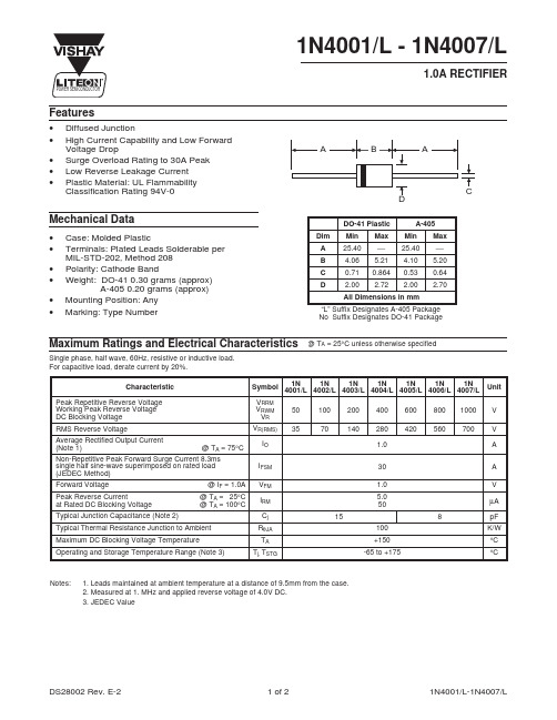
1N4001/L - 1N4007/L
1.0A RECTIFIER
POWER SEMICONDUCTOR
Features
• • • • • Diffused Junction High Current Capability and Low Forward Voltage Drop Surge Overload Rating to 30A Peak Low Reverse Leakage Current Plastic Material: UL Flammability Classification Rating 94V-0
0.6
0.4
0.1
0.2
Tj = 25ºC PULSE WIDTH = 300µs 2% DUTY CYCLE
0 40 60 80 100 120 140 160 180 TA, AMBIENT TEMPERATURE (ºC) Fig. 1 Forward Current Derating Curve
40Βιβλιοθήκη 30Cj, CAPACITANCE (pF)
1N4001 - 1N4004
10
20
1N4005 - 1N4007
10
8.3ms Single half sine-wave JEDEC Method
0 1.0 10 100 NUMBER OF CYCLES AT 60 Hz Fig. 3 Max Non-Repetitive Peak Fwd Surge Current
1N 1N 1N 1N 1N 1N 1N Symbol 4001/L 4002/L 4003/L 4004/L 4005/L 4006/L 4007/L VRRM VRWM VR VR(RMS) IO IFSM VFM IRM Cj RθJA TA Tj, TSTG 15 100 +150 -65 to +175 50 35 100 70 200 140 400 280 1.0 30 1.0 5.0 50 8 600 420 800 560 1000 700
1N4002-G;中文规格书,Datasheet资料
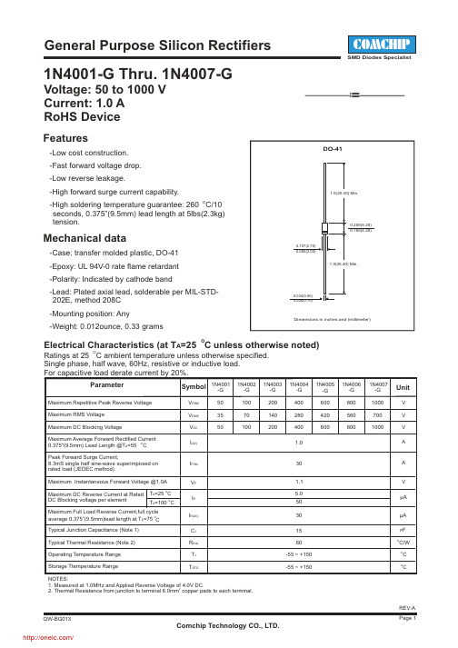
OElectrical Characteristics (at T A =25 C unless otherwise noted)ORatings at 25 C ambient temperature unless otherwise specified.Single phase, half wave, 60Hz, resistive or inductive load.For capacitive load derate current by 20%.ParameterSymbol UnitMaximum Repetitive Peak Reverse Voltage Maximum RMS Voltage Maximum DC Blocking VoltageMaximum Average Forward Rectified Current O 0.375"(9.5mm) Lead Length @T A =55C Peak Forward Surge Current, 8.3mS single half sine-wave superimposed on rated load (JEDEC method)Maximum Instantaneous Forward Voltage @1.0A Maximum DC Reverse Current at RatedOperating Temperature Range Storage Ttemperature RangeO T A =25C DC Blocking voltage per element Typical Junction Capacitance (Note 1)Typical Thermal Resistance (Note 2)503550V RRM V RMS V DC I (AV)I FSM V F I R C J R θJA T J T STG1.0305.0501560-55 ~ +150-55 ~ +150V V V AA V P FOC OCμA OC/WNOTES:1. Measured at 1.0MHz and Applied Reverse Voltage of 4.0V DC.22. Thermal Resistance from junction to terminal 6.0mm copper pads to each terminal.Voltage: 50 to 1000 V Current: 1.0 A RoHS DeviceFeatures-Low cost construction. -Fast forward voltage drop. -Low reverse leakage.-High forward surge current capability.O -High soldering temperature guarantee: 260C/10 seconds, 0.375”(9.5mm) lead length at 5lbs(2.3kg) tension.Mechanical data-Case: transfer molded plastic, DO-41 -Epoxy: UL 94V-0 rate flame retardant -Polarity: Indicated by cathode band-Lead: Plated axial lead, solderable per MIL-STD-202E, method 208C -Mounting position: Any-Weight: 0.012ounce, 0.33 grams10070100200140200400280400600420600800560800100070010001N4001-G Thru. 1N4007-G1.130-G 4001 1N -G 4002 1N -G 4003 1N -G 4004 1N -G 40051N -G 4006 1N -G 4007 1N O T A =100C Maximum Full Load Reverse Current,full cycle average 0.375”(9.5mm)lead length at T L =75 C O I R(AV)μARating and Characteristic Curves ( 1N4001) -G Thru. 4007-G1N Fig.2 Maximum. Non-Repetitive PeakForward Surge Current0ΙF S M , P e a k F o r w a r d S u r g e C u r r e n t (A )Number of Cycles at 60Hz1Fig.1 Typical Forward CurrentDerating CurveI (A V ), A v e r a g e F o r w a r d C u r r e n t (A )OT A , Ambient Temperature (C)02575175Fig.3 Typical Instantaneous ForwardCharacteristics0.01I F , I n s t a n t a n e o u s F o r w a r d C u r r e n t (A )V F , Instantaneous Forward Voltage (V)1.00.61.01.400.61.01.62.010015351.20.1Fig.4 Typical Reverse Characteristics0.01I R , I n s t a n t a n e o u s R e v e r s e C u r r e n t (m A )Percent of Peak Reverse Voltage (%)1.0100.11001250.40.80.81.8Fig.5 Typical Junction Capacitance10C J , C a p a c i t a n c e (p F )V R , Reverse Voltage (V)1000.11010010501500.21051025301.24080100140201206012010205025分销商库存信息: COMCHIP1N4002-G。
1N4007(Hitano Enterprise)中文数据手册「EasyDatasheet」

芯片中文手册,看全文,戳
奇彦企业股份有限公司. 1N4001 THRU 1N4007
特征
* 低成本 * 低泄漏 * 低正向压降 * 高电流能力
硅整流技术规范
电压范围 - 50到1000伏特Байду номын сангаас
电流 - 1.0安培
机械数据
* 案例:模压塑料 * 环氧树脂:UL 94V-0率阻燃 * 铅:MIL-STD-202E,方法208防护证 * 极性:颜色频带端为负极 * 任何安装位置: * 重量:0.33克
1N4006 800 560 800
1N4007 1000 700 1000
UNITS Volts Volts Volts
1.0
Amps
30 1.1 5.0 500
30
15 50 -65 to + 175
Amps Volts uAmps
uAmps pF C/ W C
芯片中文手册,看全文,戳 额定值和特性曲线(1N4001 1N4007 THRU)
DO-41
最大额定值,电器性能
在25℃环境温度额定值除非另有规定. 单相,半波,60赫兹,电阻或电感性负载.
对于容性负载,减免电流20%.
尺寸以英寸(毫米)
最大经常峰值反向电压
最大RMS电压
最大直流阻断电压
最大正向平均整流电流
在T = 75 C 峰值正向浪涌电流8.3ms单一正弦半波 叠加额定负荷(JEDEC方法) 最大正向电压在1.0A DC 反向电流最大DC 在额定阻断电压DC 满载最大反向电流平均值,完整周期 .375 *设计(9.5mm)引线长度在T = 75 C
典型结电容(注)
@T = 25 C @T = 100 C
YH050RMH4002

YuHua Int'l Technology co., Limited
30 31 32 33 34 35 36 37 38 39 40 DCLK DISP HS VS DE NC GND XR YD XL YU Data clk Display ON/OFF control. Internally pulled high Horizontal sync input in RGB mode Vertical sync input in RGB mode Data Enable No connection Ground T/p X-Right(No connection) T/p Y-Bottom(No connection) T/p X-Left(No connection) T/p Y-Up(No connection)
YuHua Int'l Technology co., Limited
宇华国际科技有限公司
SPECIFICATION FOR LCD MODULE
Customer :
Product Model: Sample code:
Designed by
YH050RMH4002
Checked by
Approved by
YuHua Int'l Technology co., Limited
1. General Specifications
No. 1 2 3 4 5 6 7 8 9 10 11 12 13 LCD size Driver element Resolution Display mode Dot pitch Active area Module size Surface treatment Color arrangement Interface Backlight power consumption Panel power consumption Weight Note 1: Refer to Mechanical Drawing. Item Specification 5.0 inch(Diagonal) a-Si TFT active matrix 800× 3(RGB) × 480 Normally White, Transmissive 0.135(W) ×0.135(H) mm 108(W) ×64.8 (H) mm 120.7(W) ×75.8(H) ×4.2(D) Anti-Glare RGB-stripe Digital TBD TBD TBD mm Note 1 Remark
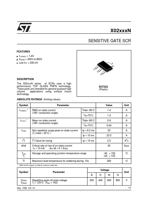
X02xxxN中文资料
Sensitivity
02
03
05
20
20
200
200
50
0.8
0.1
8 0.5
5
6
1.5
5
200
15
20
15
100
Fig.8 : On-state characteristics (maximum values).
I TSM (A). I2 t (A2 s) 100
ITSM 10
I2 t
1 1
Tj initial = 25oC
tp(ms) 10
I TM (A) 100
Tj initial 25oC
10
Tj max
The ST logo is a trademark of STMicroelectronics
VD=67%VDRM RGK = 1 KΩ
ITM= 3 x IT(AV) VR=35V dI/dt=10A/µs tp=100µs dV/dt=2V/µs VD= 67%VDRM RGK = 1 KΩ
Tj= 25°C MIN MAX
Tj= 25°C MAX Tj= 125°C MIN
Tj= 25°C MIN Tj= 25°C TYP
0.8
= 180o
0.6
0.4
0.2 0.0
0
Ttab (oC) 10 20 30 40 50 60 70 80 90 100 110 120 130
Fig.4 : Relative variation of thermal impedance junction to ambient versus pulse duration.
霍尼韦尔氢气纯度仪说明书模板
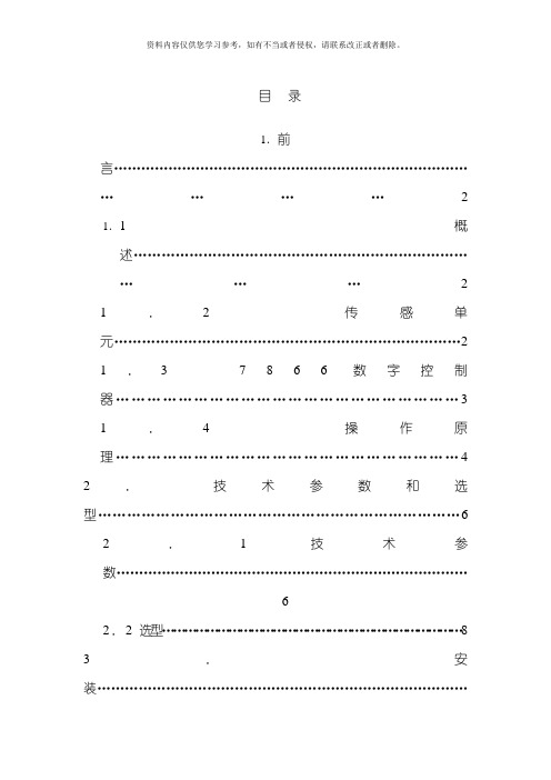
目录1.前言………………………………………………………………………………2 1.1概述……………………………………………………………….........2 1.2传感单元 (2)1.37866数字控制器 (3)1.4操作原理 (4)2.技术参数和选型 (6)2.1技术参数……………………………………………………………………62.2选型 (8)3.安装……………………………………………………………………….........9 3.1传感单元要求条件和定位 (9)3.2安装传感单元 (9)3.3管路连接 (9)3.4传感单元与数字控制器接线 (10)4.设置模式………………………………………………………………………11 4.1概述………………………………………………………………………11 4.2结构概述……………………………………………………………………...11 4.3单元设置组群 (11)4.4报警设置组群 (12)4.5M o d B U S通讯设置组群 (12)4.6校准组群………………………………………………………………………13 4.7状态组群………………………………………………………………………13 5.校准……………………………………………………………………………14 5.1概述……………………………………………………………………...14 5.2传感单元校准 (14)5.37866分析仪输入校准 (14)5.4模拟输出校准 (15)5.7安全锁定……………………………………………………………………...16 5.8设置报警极限 (17)6.操作………………………………………………………………………………18 6.1启动………………………………………………………………………18 7.排除故障…………………………………………………………………………19 7.1概述……………………………………………………………………...19 7.27866数字控制器检测 (20)附录 (21)1.前言1.1 概述美国HONEYWELL公司7866氢气纯度分析仪由三个基本部件组成: 传感单元( 变送器) , 控制单元( 接收器) ( 图1-1) 和电源。
自制变压器和稳压电源

1 变压器的工作原理
要想弄清变压器的原理,得从一个实验说起。图 31 是在 一个接有电流表的线圈内插入磁铁的情况。没有插入磁铁或磁 铁放入线圈不动时,电流表中都没有电流。在插入磁铁的过程 中,电流表中有电流指示,指针偏向一方;在拔出磁铁的过程 中电流表也有电流指示,指针偏向另一方。这说明插入和拔出 磁铁时线圈内都被感应出电流,而且两种情况感应出的电流方 向不同。这一实验表明线圈内没有磁场或磁场不变化,线圈里
37
的 19 号漆包线并绕; I6V 采用两 根Φ 1.51mm 的 17 号漆包线并 12V 绕;I10V 采用单根Φ1.73mm 的 Φ1.51 12 圈 10V 16 号漆包线; I12V 采用单根Φ 220V Φ0.36 Φ1.73 25 圈 1.51mm 的 17 号漆包线。 1298 圈 6V 次级有多种输出电压时,可 2Φ1.51 6圈 5V 绕多个次级线圈。但多个线圈用 4Φ1.15 12 圈 3V 铜线多,线圈会增厚,硅钢片的 4Φ1.51 19 圈 0 窗口可能容纳不下。如果对变压 器没有特殊要求,也可多种电压 图 36 举例设计变压器数据 由一个带抽头的次级线圈输出。图 3-6 是设计举例的变压器, 采用的就是带抽头的次级线圈。 为了设计变压器更加简便,本书将小功率变压器的一些数 据列于表 32,只要获得了铁芯,在表中查出相应的数据,就 会得到每伏圈数,然后再根据电压计算出圈数和线径,就可进 行绕制了。
0.005 0.007 0.010 0.013 0.016 0.020 0.024 0.030 0.033 0.039 0.044 0.050 0.057 0.064 0.071 0.079 0.087 0.105 0.122 0.143 0.165 0.187 0.212
1N4002L中文资料
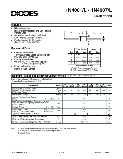
Features1N4001/L - 1N4007/L1.0A RECTIFIER“L” Suffix Designates A-405 Package No Suffix Designates DO-41 Package AAB CDDO-41 PlasticA-405Dim Min Max Min Max A 25.40¾25.40¾B 4.06 5.21 4.10 5.20C 0.710.8640.530.64D2.002.722.002.70All Dimensions in mmMaximum Ratings and Electrical Characteristics@ T A = 25°C unless otherwise specified·Diffused Junction·High Current Capability and Low Forward Voltage Drop·Surge Overload Rating to 30A Peak ·Low Reverse Leakage Current ·Plastic Material: UL Flammability Classification Rating 94V-0Mechanical Data·Case: Molded Plastic·Terminals: Plated Leads Solderable per MIL-STD-202, Method 208·Polarity: Cathode Band·Weight: DO-41 0.30 grams (approx)A-405 0.20 grams (approx)·Mounting Position: Any ·Marking: Type NumberSingle phase, half wave, 60Hz, resistive or inductive load.For capacitive load, derate current by 20%.CharacteristicSymbol 1N 4001/L 1N 4002/L 1N 4003/L 1N 4004/L1N 4005/L 1N 4006/L 1N 4007/L Unit Peak Repetitive Reverse Voltage Working Peak Reverse Voltage DC Blocking Voltage V RRMV RWM V R 501002004006008001000V RMS Reverse VoltageV R(RMS)3570140280420560700V Average Rectified Output Current (Note 1)@ T A = 75°C I O 1.0A Non-Repetitive Peak Forward Surge Current 8.3ms single half sine-wave superimposed on rated load (JEDEC Method)I FSM 30A Forward Voltage@ I F = 1.0A V FM 1.0V Peak Reverse Current@ T A = 25°C at Rated DC Blocking Voltage @ T A = 100°CI RM 5.050m A Typical Junction Capacitance (Note 2)C j 158pF Typical Thermal Resistance Junction to Ambient R q JA 100K/W Maximum DC Blocking Voltage Temperature T A +150°C Operating and Storage Temperature Range (Note 3)T j,T STG-65 to +175°CNotes:1. Leads maintained at ambient temperature at a distance of 9.5mm from the case.2. Measured at 1.MHz and applied reverse voltage of 4.0V DC.3. JEDEC Value .4060801001201401601800.20.40.60.81.0I ,A V E R A G E F O R W A R D R E C T I F I E D C U R R E N T (A )(A V )T ,AMBIENT TEMPERATURE (ºC)Fig.1Forward Current Derating CurveA C ,C A P A C I T A N C E (p F )j V ,REVERSE VOLTAGE (V)Fig.4Typical Junction CapacitanceR 1.0101001.0101001.010100I ,P E AK F O R W A R D S U R G E C U R R E N T (A )F S M NUMBER OF CYCLES AT 60HzFig.3Max Non-Repetitive Peak Fwd Surge Current403020010500.60.8 1.0 1.2 1.4 1.60.010.11.0I ,I N S T AN T A N E O U S F O R W A R D C U R R E N T (A )F V ,INSTANTANEOUS FORWARD VOLTAGE (V)Fig.2Typical Forward CharacteristicsF 10。
1N4004(compact)中文数据手册「EasyDatasheet」

UNIT
VRRM
50
VRMS
35
VDC
50
100 200 400 600 800 1000 V
70
140
280 420
560
700 V
100 200 400 600 800 1000 V
@T A=75 C I(AV)
1.0
A
IFSM
30
A
VF
@T J=25 C
IR
@T J=100 C
CJ
1.1
V
5
50
Resistive or Inductive Load
.2 0.375" (9.5mm)
Lead Length
AVERAGE FORWARD RECTIFIED CURRENT AMPERES 0 0 25 50 75 100 125 150 175 AMBIENT TEMPERATURE. ( OC)
1
2
4 6 8 10
20
40 6 0 80 100
NUMBER OF CYCLES AT 60Hz
FIG.4- TYPICAL JUNCTION CAPACITANCE
100
60 40
20
10
6
Tj=25 CO
JUNCTION CAPACITANCE.(pF)
4
2
1 .1 .2 .4
1.0 2 4
10 20 40 100
特性
最大的经常峰值反向电压
最大RMS电压
最大直流阻断电压 最大正向平均 整流电流
峰值正向浪涌电流
8.3ms单半正弦波 超级施加额定负荷(JEDEC的方法)
最大正向电压在1.0A DC 反向电流最大DC 在额定阻断电压DC
M54HC4002中文资料

M54HC4002M74HC4002October 1992DUAL 4INPUT NOR GATEB1R(Plastic Package)ORDER CODES :M54HC4002F1R M74HC4002M1R M74HC4002B1R M74HC4002C1RF1R(Ceramic Package)M1R(Micro Package)C1R (Chip Carrier)PIN CONNECTIONS (top view)NC =No Internal Connecti o nINPUT AND OUTPUT EQUIVALENT CIRCUITDESCRIPTION.HIGH SPEEDt PD =10ns (TYP.)AT V CC =5V .LOW POWER DISSIPATION I CC =1µA (MAX.)AT T A =25°C .HIGH NOISE IMMUNITYV NIH =V NIL =28%V CC (MIN.).OUTPUT DRIVE CAPABILITY 10LSTTL LOADS.SYMMETRICAL OUTPUT IMPEDANCE |I OH |=I OL =4mA (MIN.).BALANCED PROPAGATION DELAYS t PLH =t PHL.WIDE OPERATING VOLTAGE RANGE V CC (OPR)=2V TO 6V.PIN AND FUNCTION COMPATIBLE WITH 4002BThe M54/74HC4002is a high speed CMOS DUAL 4-INPUT NOR GATE fabricated in silicon gate C 2MOS technology.It has the same high speed performance of LSTTL combined with true CMOS low power consumption.The internal circuit is composed of 3stages includ-ing buffer output,which ensures high noise im-munity and stable output.All inputs are equipp ed with protection circuits against static discharge and transient excess volt-age.1/9M54/M74HC4002TRUTH TABLEIEC LOGIC SYMBOLnA nB nC nD nYL L L L HH X X X LX H X X LX X H X LX X X H LPIN DESCRIPTIONPIN No SYMBOL NAME AND FUNCTION1,131Y to2Y Data Outputs2,91A to2A Data Inputs3,101B to2B Data Inputs4,111C to2C Data Inputs5,121D to4D Data Inputs6,8NC Not Connected7GND Ground(0V)14V CC Positive Supply VoltageSCHEMATIC CIRCUIT(Per Gate)ABSOLUTE MAXIMUM RATINGSymbol Parameter Value Unit V CC Supply Voltage-0.5to+7V V I DC Input Voltage-0.5to V CC+0.5V V O DC Output Voltage-0.5to V CC+0.5VI IK DC Input Diode Current±20mAI OK DC Output Diode Current±20mAI O DC Output Source Sink Current Per Output Pin±25mAI CC or I GND DC V CC or Ground Current±50mAP D Power Dissipation500(*)mW T stg Storage Temperature-65to+150o C T L Lead Temperature(10sec)300o C Absolute Maximum Ratings are those values beyond whichdamage to the device may occu r.Functiona l ope ration und er these cond ition isnotimplied. (*)500mW:≅65o C derate to300mW by10mW/o C:65o C to85o C2/9RECOMMENDED OPERATING CONDITIONSSymbol Parameter Value Unit V CC Supply Voltage2to6V V I Input Voltage0to V CC V V O Output Voltage0to V CC VT op Operating Temperature:M54HC SeriesM74HC Series -55to+125-40to+85o Co Ct r,t f Input Rise and Fall Time V CC=2V0to1000nsV CC=4.5V0to500V CC=6V0to400DC SPECIFICATIONSSymbol ParameterTest Conditions ValueUnit V CC(V)T A=25o C54HC and74HC-40to85o C74HC-55to125o C54HCMin.Typ.Max.Min.Max.Min.Max.V IH High Level InputVoltage 2.0 1.5 1.5 1.5V 4.5 3.15 3.15 3.156.0 4.2 4.2 4.2V IL Low Level InputVoltage 2.00.50.50.5V 4.5 1.35 1.35 1.356.0 1.8 1.8 1.8V OH High LevelOutput Voltage 2.0V I=V IHorV ILI O=-20µA1.92.0 1.9 1.9V 4.5 4.4 4.5 4.4 4.46.0 5.9 6.0 5.9 5.94.5I O=-4.0mA 4.18 4.31 4.13 4.106.0I O=-5.2mA 5.68 5.8 5.63 5.60V OL Low Level OutputVoltage 2.0V I=V IHorV ILI O=20µA0.00.10.10.1V 4.50.00.10.10.16.00.00.10.10.14.5I O=4.0mA0.170.260.330.406.0I O=5.2mA0.180.260.330.40I I Input LeakageCurrent 6.0V I=V CC or GND±0.1±1±1µAI CC Quiescent SupplyCurrent 6.0V I=V CC or GND11020µAM54/M74HC40023/9AC ELECTRICAL CHARACTERISTICS (C L =50pF,Input t r =t f =6ns)SymbolParameterTest ConditionsValueUnitV CC (V)T A =25o C 54HC and 74HC -40to 85o C 74HC -55to 125o C54HC Min.Typ.Max.Min.Max.Min.Max.t TLH t THL Output Transition Time 2.0307595110ns 4.581519226.07131619t PLH t PHLPropagation Delay Time2.048100125150ns 4.5122025306.010172126C IN Input Capacitance 5101010pF C PD (*)Power Dissipation Capacitance20pF (*)C PD is defined as the value of the IC’s internal equivalent capac itanc e which is calculated from the operating current con sump tion without load.(Refer to Test Circuit).Average operting current can be obtained by the following equ ation.I CC (opr)=C PD •V CC •f IN +I CC /4(per Gate)SWITCHING CHARACTERISTICS TEST CIRCUITINPUT WAVEFORM IS THE SAME AS THAT IN CASE OF SWITCHING CHARACTERIS TICS TEST.TEST CIRCUIT I CC (Opr.)M54/M74HC40024/9M54/M74HC4002 Plastic DIP14MECHANICAL DATAmm inchDIM.MIN.TYP.MAX.MIN.TYP.MAX.a10.510.020B 1.39 1.650.0550.065b0.50.020b10.250.010D200.787E8.50.335e 2.540.100e315.240.600F7.10.280I 5.10.201L 3.30.130Z 1.27 2.540.0500.100P001A5/9M54/M74HC4002Ceramic DIP14/1MECHANICAL DATAmm inch DIM.MIN.TYP.MAX.MIN.TYP.MAX.A200.787 B7.00.276D 3.30.130E0.380.015e315.240.600F 2.29 2.790.0900.110G0.40.550.0160.022H 1.17 1.520.0460.060L0.220.310.0090.012 M 1.52 2.540.0600.100 N10.30.406 P7.88.050.3070.317 Q 5.080.200P053C 6/9M54/M74HC4002SO14MECHANICAL DATAmm inchDIM.MIN.TYP.MAX.MIN.TYP.MAX.A 1.750.068a10.10.20.0030.007a2 1.650.064b0.350.460.0130.018b10.190.250.0070.010C0.50.019c145°(typ.)D8.558.750.3360.344E 5.8 6.20.2280.244e 1.270.050e37.620.300F 3.8 4.00.1490.157G 4.6 5.30.1810.208L0.5 1.270.0190.050M0.680.026S8°(max.)P013G7/9M54/M74HC4002PLCC20MECHANICAL DATAmm inch DIM.MIN.TYP.MAX.MIN.TYP.MAX.A9.7810.030.3850.395 B8.899.040.3500.356D 4.2 4.570.1650.180d1 2.540.100d20.560.022E7.378.380.2900.330e 1.270.050e3 5.080.200F0.380.015G0.1010.004 M 1.270.050M1 1.140.045P027A 8/9M54/M74HC4002 Information furnished is believed to be accurate and reliable.However,SGS-THOMSON Microelectronics assumes no responsability for the consequences of use of such information nor for any infringement of patents or other rights of third parties which may results from its use.No license is granted by implication or otherwise under any patent or patent rights of SGS-THOMSON Microelectronics.Specificationsmentioned in this publication are subject to change without notice.This publication supersedes and replaces all information previously supplied.SGS-THOMSON Microelectronics products are not authorized for use ascritical components in life support devices or systems without express written approval of SGS-THOMSON Microelectonics.©1994SGS-THOMSON Microelectronics-All Rights ReservedSGS-THOMSON Microelectronics GROUP OF COMPANIESAustralia-Brazil-France-Germany-Hong Kong-Italy-Japan-Korea-Malaysia-Malta-Morocco-The Netherlands-Singapore-Spain-Sweden-Switzerland-Taiwan-Thailand-United Kingdom-U.S.A9/9。
1N4007RLG;1N4002RLG;1N4004RLG;1N4005RLG;1N4003RLG;中文规格书,Datasheet资料
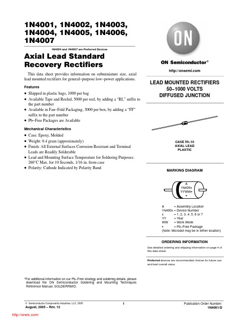
1N4001, 1N4002, 1N4003,1N4004, 1N4005, 1N4006,1N40071N4004 and 1N4007 are Preferred DevicesAxial Lead Standard Recovery RectifiersThis data sheet provides information on subminiature size, axial lead mounted rectifiers for general−purpose low−power applications. Features•Shipped in plastic bags, 1000 per bag•Available Tape and Reeled, 5000 per reel, by adding a “RL” suffix to the part number•Available in Fan−Fold Packaging, 3000 per box, by adding a “FF”suffix to the part number•Pb−Free Packages are AvailableMechanical Characteristics•Case: Epoxy, Molded•Weight: 0.4 gram (approximately)•Finish: All External Surfaces Corrosion Resistant and Terminal Leads are Readily Solderable•Lead and Mounting Surface Temperature for Soldering Purposes: 260°C Max. for 10 Seconds, 1/16 in. from case •Polarity: Cathode Indicated by Polarity Band*For additional information on our Pb−Free strategy and soldering details, please download the ON Semiconductor Soldering and Mounting Techniques Reference Manual, SOLDERRM/D.CASE 59−10AXIAL LEADPLASTICLEAD MOUNTED RECTIFIERS50−1000 VOLTSDIFFUSED JUNCTIONPreferred devices are recommended choices for future use and best overall value.MARKING DIAGRAMSee detailed ordering and shipping information on page 4 of this data sheet.ORDERING INFORMATIONA= Assembly Location1N400x= Device Numberx= 1, 2, 3, 4, 5, 6 or 7YY= YearWW= Work WeekG= Pb−Free Package(Note: Microdot may be in either location)A1N400xYYWW GGMAXIMUM RATINGSRating Symbol1N40011N40021N40031N40041N40051N40061N4007Unit†Peak Repetitive Reverse Voltage Working Peak Reverse Voltage DC Blocking Voltage V RRMV RWMV R501002004006008001000V†Non−Repetitive Peak Reverse Voltage(halfwave, single phase, 60 Hz)V RSM6012024048072010001200V †RMS Reverse Voltage V R(RMS)3570140280420560700V†Average Rectified Forward Current(single phase, resistive load,60 Hz, T A = 75°C)I O 1.0A†Non−Repetitive Peak Surge Current(surge applied at rated load conditions)I FSM30 (for 1 cycle)AOperating and Storage Junction Temperature RangeT JT stg−65 to +175°CMaximum ratings are those values beyond which device damage can occur. Maximum ratings applied to the device are individual stress limit values (not normal operating conditions) and are not valid simultaneously. If these limits are exceeded, device functional operation is not implied, damage may occur and reliability may be affected.ELECTRICAL CHARACTERISTICS†Rating Symbol Typ Max Unit Maximum Instantaneous Forward Voltage Drop, (i F = 1.0 Amp, T J = 25°C)v F0.93 1.1V Maximum Full−Cycle Average Forward Voltage Drop, (I O = 1.0 Amp, T L = 75°C, 1 inch leads)V F(AV)−0.8VMaximum Reverse Current (rated DC voltage) (T J = 25°C)(T J = 100°C)I R0.051.01050m AMaximum Full−Cycle Average Reverse Current, (I O = 1.0 Amp, T L = 75°C, 1 inch leads)I R(AV)−30m A †Indicates JEDEC Registered Data10.110I F , F O R W A R D C U R R E N T (A )Figure 3. Typical CapacitanceV R , REVERSE VOLTAGE (V)1N4001Axial Lead*1000 Units/Bag1N4001G Axial Lead*1000 Units/Bag(Pb−Free)1N4001FF Axial Lead*3000 Units/Box3000 Units/Box1N4001FFG Axial Lead*(Pb−Free)1N4001RL Axial Lead*5000/T ape & Reel5000/T ape & Reel1N4001RLG Axial Lead*(Pb−Free)1N4002Axial Lead*1000 Units/Bag1000 Units/Bag1N4002G Axial Lead*(Pb−Free)1N4002FF Axial Lead*3000 Units/Box3000 Units/Box1N4002FFG Axial Lead*(Pb−Free)1N4002RL Axial Lead*5000/T ape & Reel5000/T ape & Reel1N4002RLG Axial Lead*(Pb−Free)1N4003Axial Lead*1000 Units/Bag1N4003G Axial Lead*1000 Units/Bag(Pb−Free)1N4003FF Axial Lead*3000 Units/Box3000 Units/Box1N4003FFG Axial Lead*(Pb−Free)1N4003RL Axial Lead*5000/T ape & Reel5000/T ape & Reel1N4003RLG Axial Lead*(Pb−Free)1N4004Axial Lead*1000 Units/Bag1000 Units/Bag1N4004G Axial Lead*(Pb−Free)1N4004FF Axial Lead*3000 Units/Box3000 Units/Box1N4004FFG Axial Lead*(Pb−Free)1N4004RL Axial Lead*5000/T ape & Reel5000/T ape & Reel1N4004RLG Axial Lead*(Pb−Free)1N4005Axial Lead*1000 Units/Bag1N4005G Axial Lead*1000 Units/Bag(Pb−Free)1N4005FF Axial Lead*3000 Units/Box3000 Units/Box1N4005FFG Axial Lead*(Pb−Free)1N4005RL Axial Lead*5000/T ape & Reel5000/T ape & Reel1N4005RLG Axial Lead*(Pb−Free)†For information on tape and reel specifications, including part orientation and tape sizes, please refer to our Tape and Reel Packaging Specifications Brochure, BRD8011/D.*This package is inherently Pb−Free.1N4006Axial Lead*1000 Units/Bag1000 Units/Bag1N4006G Axial Lead*(Pb−Free)1N4006FF Axial Lead*3000 Units/Box3000 Units/Box1N4006FFG Axial Lead*(Pb−Free)1N4006RL Axial Lead*5000/T ape & Reel1N4006RLG Axial Lead*5000/T ape & Reel(Pb−Free)1N4007Axial Lead*1000 Units/Bag1000 Units/Bag1N4007G Axial Lead*(Pb−Free)1N4007FF Axial Lead*3000 Units/Box3000 Units/Box1N4007FFG Axial Lead*(Pb−Free)1N4007RL Axial Lead*5000/T ape & Reel1N4007RLG Axial Lead*5000/T ape & Reel(Pb−Free)†For information on tape and reel specifications, including part orientation and tape sizes, please refer to our Tape and Reel Packaging Specifications Brochure, BRD8011/D.*This package is inherently Pb−Free.PACKAGE DIMENSIONSAXIAL LEAD CASE 59−10ISSUE UDIM MIN MAX MIN MAX MILLIMETERSINCHES A 4.10 5.200.1610.205B 2.00 2.700.0790.106D 0.710.860.0280.034F −−− 1.27−−−0.050K25.40−−−1.000−−−NOTES:1.DIMENSIONING AND TOLERANCING PER ANSI Y14.5M, 1982.2.CONTROLLING DIMENSION: INCH.3.ALL RULES AND NOTES ASSOCIATED WITH JEDEC DO−41 OUTLINE SHALL APPLY4.POLARITY DENOTED BY CATHODE BAND.5.LEAD DIAMETER NOT CONTROLLED WITHIN F DIMENSION.ON Semiconductor and are registered trademarks of Semiconductor Components Industries, LLC (SCILLC). SCILLC reserves the right to make changes without further noticeto any products herein. SCILLC makes no warranty, representation or guarantee regarding the suitability of its products for any particular purpose, nor does SCILLC assume any liability arising out of the application or use of any product or circuit, and specifically disclaims any and all liability, including without limitation special, consequential or incidental damages.“Typical” parameters which may be provided in SCILLC data sheets and/or specifications can and do vary in different applications and actual performance may vary over time. All operating parameters, including “Typicals” must be validated for each customer application by customer’s technical experts. SCILLC does not convey any license under its patent rights nor the rights of others. SCILLC products are not designed, intended, or authorized for use as components in systems intended for surgical implant into the body, or other applications intended to support or sustain life, or for any other application in which the failure of the SCILLC product could create a situation where personal injury or death may occur. Should Buyer purchase or use SCILLC products for any such unintended or unauthorized application, Buyer shall indemnify and hold SCILLC and its officers, employees, subsidiaries, affiliates,and distributors harmless against all claims, costs, damages, and expenses, and reasonable attorney fees arising out of, directly or indirectly, any claim of personal injury or death associated with such unintended or unauthorized use, even if such claim alleges that SCILLC was negligent regarding the design or manufacture of the part. SCILLC is an Equal Opportunity/Affirmative Action Employer. This literature is subject to all applicable copyright laws and is not for resale in any manner.PUBLICATION ORDERING INFORMATION分销商库存信息:ONSEMI1N4007RLG1N4002RLG1N4004RLG 1N4005RLG1N4003RLG1N4001RLG 1N4004G1N4007G1N4001G1N4002G1N4003G1N4006G1N4005G1N4001RL1N4002RL 1N4003RL1N4004RL1N4005RL 1N4006RL1N4006RLG1N4007RL。
ULN2004AIDRE4资料

PACKAGING INFORMATIONOrderable Device Status (1)Package Type Package DrawingPins Package Qty Eco Plan (2)Lead/Ball Finish MSL Peak Temp (3)ULN2004AID ACTIVE SOIC D 1640Green (RoHS &no Sb/Br)CU NIPDAU Level-1-260C-UNLIM ULN2004AIDE4ACTIVE SOIC D 1640Green (RoHS &no Sb/Br)CU NIPDAU Level-1-260C-UNLIM ULN2004AIDR ACTIVE SOIC D 162500Green (RoHS &no Sb/Br)CU NIPDAU Level-1-260C-UNLIM ULN2004AIDRE4ACTIVE SOIC D 162500Green (RoHS &no Sb/Br)CU NIPDAU Level-1-260C-UNLIM ULN2004AIN ACTIVE PDIP N 1625Pb-Free (RoHS)CU NIPDAU N /A for Pkg Type ULN2004AINE4ACTIVE PDIP N 1625Pb-Free (RoHS)CU NIPDAU N /A for Pkg Type ULN2004AINSR ACTIVE SO NS 162000Green (RoHS &no Sb/Br)CU NIPDAU Level-1-260C-UNLIM ULN2004AINSRE4ACTIVESONS162000Green (RoHS &no Sb/Br)CU NIPDAULevel-1-260C-UNLIM(1)The marketing status values are defined as follows:ACTIVE:Product device recommended for new designs.LIFEBUY:TI has announced that the device will be discontinued,and a lifetime-buy period is in effect.NRND:Not recommended for new designs.Device is in production to support existing customers,but TI does not recommend using this part in a new design.PREVIEW:Device has been announced but is not in production.Samples may or may not be available.OBSOLETE:TI has discontinued the production of the device.(2)Eco Plan -The planned eco-friendly classification:Pb-Free (RoHS),Pb-Free (RoHS Exempt),or Green (RoHS &no Sb/Br)-please check /productcontent for the latest availability information and additional product content details.TBD:The Pb-Free/Green conversion plan has not been defined.Pb-Free (RoHS):TI's terms "Lead-Free"or "Pb-Free"mean semiconductor products that are compatible with the current RoHS requirements for all 6substances,including the requirement that lead not exceed 0.1%by weight in homogeneous materials.Where designed to be soldered at high temperatures,TI Pb-Free products are suitable for use in specified lead-free processes.Pb-Free (RoHS Exempt):This component has a RoHS exemption for either 1)lead-based flip-chip solder bumps used between the die and package,or 2)lead-based die adhesive used between the die and leadframe.The component is otherwise considered Pb-Free (RoHS compatible)as defined above.Green (RoHS &no Sb/Br):TI defines "Green"to mean Pb-Free (RoHS compatible),and free of Bromine (Br)and Antimony (Sb)based flame retardants (Br or Sb do not exceed 0.1%by weight in homogeneous material)(3)MSL,Peak Temp.--The Moisture Sensitivity Level rating according to the JEDEC industry standard classifications,and peak solder temperature.Important Information and Disclaimer:The information provided on this page represents TI's knowledge and belief as of the date that it is provided.TI bases its knowledge and belief on information provided by third parties,and makes no representation or warranty as to the accuracy of such information.Efforts are underway to better integrate information from third parties.TI has taken and continues to take reasonable steps to provide representative and accurate information but may not have conducted destructive testing or chemical analysis on incoming materials and chemicals.TI and TI suppliers consider certain information to be proprietary,and thus CAS numbers and other limited information may not be available for release.In no event shall TI's liability arising out of such information exceed the total purchase price of the TI part(s)at issue in this document sold by TI to Customer on an annual basis.PACKAGE OPTION ADDENDUM5-Feb-2007Addendum-Page 1IMPORTANT NOTICETexas Instruments Incorporated and its subsidiaries (TI) reserve the right to make corrections, modifications, enhancements, improvements, and other changes to its products and services at any time and todiscontinue any product or service without notice. Customers should obtain the latest relevant informationbefore placing orders and should verify that such information is current and complete. All products are soldsubject to TI’s terms and conditions of sale supplied at the time of order acknowledgment.TI warrants performance of its hardware products to the specifications applicable at the time of sale inaccordance with TI’s standard warranty. Testing and other quality control techniques are used to the extentTI deems necessary to support this warranty. Except where mandated by government requirements, testingof all parameters of each product is not necessarily performed.TI assumes no liability for applications assistance or customer product design. Customers are responsiblefor their products and applications using TI components. To minimize the risks associated with customerproducts and applications, customers should provide adequate design and operating safeguards.TI does not warrant or represent that any license, either express or implied, is granted under any TI patentright, copyright, mask work right, or other TI intellectual property right relating to any combination, machine,or process in which TI products or services are used. Information published by TI regarding third-partyproducts or services does not constitute a license from TI to use such products or services or a warranty orendorsement thereof. Use of such information may require a license from a third party under the patents orother intellectual property of the third party, or a license from TI under the patents or other intellectualproperty of TI.Reproduction of information in TI data books or data sheets is permissible only if reproduction is withoutalteration and is accompanied by all associated warranties, conditions, limitations, and notices.Reproduction of this information with alteration is an unfair and deceptive business practice. TI is notresponsible or liable for such altered documentation.Resale of TI products or services with statements different from or beyond the parameters stated by TI forthat product or service voids all express and any implied warranties for the associated TI product or serviceand is an unfair and deceptive business practice. TI is not responsible or liable for any such statements.Following are URLs where you can obtain information on other Texas Instruments products and applicationsolutions:Products ApplicationsAmplifiers Audio /audioData Converters Automotive /automotive/broadbandBroadbandDSP DigitalControl /digitalcontrol Interface Military /military Logic Power Mgmt Optical Networking /opticalnetworkSecurity /security Microcontrollers Low Power Wireless /lpw Telephony /telephonyVideo & Imaging /video/wirelessWirelessMailing Address: Texas InstrumentsPost Office Box 655303 Dallas, Texas 75265Copyright © 2007, Texas Instruments Incorporated。
BTS-4002(Chinese)
电池综合测试仪BTS-4002用户手册版本:1.0深圳市泰斯电子有限公司2012年3月l 在第一次使用本产品前,请详细阅读【用户手册】。
l 本机所附电源线内包含安全接地线,请确保电源插座安全接地线接地良好,在生产线场合固定使用时,请使用额外接地线连接机器后背板的安全接地螺丝孔。
l 本测试仪电路设计上不支持电池反接,在连接电池到电池测试仪前,请确认电池正负极和测试仪正负极连接线是否正确,如果反接,可能会因为电池放电电流过大导致电池或者测试仪器损坏。
l 本测试仪支持用户调整测试仪内部散热风扇运转速度,在环境温度高以及高负荷连续使用测试仪情况下,请勿将测试仪风扇速度设置为0,以免测试仪内部温度过高,影响测试精度或者导致测试仪故障。
l 本测试仪内无任何用户可以调整更换的零件或者保险丝等易损件,在未得到本公司书面许可情况下,严禁私自打开机壳,否则会影响设备保修目录1 产品概述 42 外观特性 52.1 前面板设计 52.2 键盘界面 62.3 接线端口72.4 后背板设计83 开机界面94 测试项目和参数设置104.1 参数说明104.2 测试功能描述124.3 测试步骤设置215 选项设置235.1 测试选项235.2 条码选项265.3 其他选项(信号指示)285.4 通信选项296 测试操作306.1 电池接线方式306.2 启动触发信号316.3 输出信号326.4 测试界面显示336.5 历史数据查看357 校准操作367.1 电压校准367.2 电压电流校准377.3 内阻校准387.4 其他参数校准398 特性指标401. 产品概述电池综合测试仪是一种能够快速检测电池的各项性能参数的专用测试设备,主要应用于电池生产厂家的电池生产检测,电池应用厂家电池来料检验等等用途,能够快速鉴别电池的性能指标,性能参数是否符合要求,能够根据设定参数快速判断电池是否为合格品。
深圳市泰斯电子有限公司成立多年,从最早第一代电池测试仪产品BTS-2002系列推向市场以来,得到电池生产厂家一致认同和广泛应用,在客户的大批量使用条件下,结合实际产品,不断升级;改善,从最早的1.0版本到最新的BTS-2002H的V5.9版,性能不断升级,在BTS-2002H基础上,升级到BTS-3002版本,也得到很多高端客户的认同,BTS-4002系列产品是在结合前两代的基础和优势下,新推出的最新一代电池测试仪产品,完全采用全新的设计,主控芯片采用ST公司新推出的32位ARM处理器,模拟器件采用ADI的高速16位模拟数字转换芯片,在整体精度和性能上有脱胎换骨的表现,具体表现在测试精度更高,测试速度更快,用户设置自定义更灵活,支持测试步骤自定义等等一系列的人性化改造升级。
ADF4002资料

PHASE FREQUENCY DETECTOR
CHARGE PUMP
CP
LOCK DETECT
CURRENT SETTING 1
CURRENT SETTING 2
CPI3 CPI2 CPI1 CPI6 CPI5 CPI4
AVDD SDOUT
MUX
HIGH Z
MUXOUT
REFIN
CLK DATA
LE
RFINA RFINB
AVDD DVDD
24-BIT INPUT REGISTER 22 SDOUT
FUNCTIONAL BLOCK DIAGRAM
VP CPGND
REFERENCE
RSET
14-BIT R COUNTER
14 R COUNTER
LATCH
FUNCTION LATCH
One Technology Way, P.O. Box 9106, Norwood, MA 02062-9106, U.S.A.
Tel: 781.329.4700
Fax: 781.461.3113
©2006 Analog Devices, Inc. All rights reserved.
Thermal Characteristics .............................................................. 5 ESD Caution.................................................................................. 5 Pin Configurations and Function Descriptions ........................... 6 Typical Performance Characteristics ............................................. 7 Theory of Operation ........................................................................ 8 Reference Input Section............................................................... 8 RF Input Stage............................................................................... 8 N Counter...................................................................................... 8 R Counter ...................................................................................... 8 Phase Frequency Detector (PFD) and Charge Pump.............. 8
HO4002-1;中文规格书,Datasheet资料

Electrical Characteristics CharacteristicSymNotesMinimumTypicalMaximumUnitsOperating FrequencyAbsoluteFrequency f O1, 7400.00MHz Tune Range 399.960400.040MHz Tune Voltage 0+10VDC Tuning Linearity3:14:1RF Output Power P O3, 6+7+10dBmDiscrete SpuriousSecond Harmonics2, 3, 4-15dBcThird and Higher Harmonics-20Nonharmonic -80SSB Phase Noise1 kHz Offset -100-95dBc/Hz 10 kHz Offset -130-125100 kHz Offset-150RF ImpedanceNominal Impedance Z O 350ΩOperating Load VSWR G L 3, 52:1DC Power SupplyOperating Voltage V CC 3, 610.81213.2VDC Operating CurrentI CC 45mA Operating Case TemperatureT C3, 6-20+70°C Lid Symbolization (YY=Year, WW=Week)RFM HO4002-1 YYWW•SAW Frequency Stabilization•Fundamental-Mode Oscillation at 400.0 MHz •A Rugged, Compact General-Purpose Oscillator •Complies with Directive 2002/95/EC (RoHS)The frequency of this oscillator is stabilized by surface-acoustic-wave (SAW) technology. This results in excellent performance from a compact, rugged, oscillator operating at the fundamental frequency of 400.0 MHz. The high-reliability of the HO4002-1 makes it suitable for general purpose use in a wide variety of applications.Absolute Maximum Ratings RatingValueUnitsDC Supply Voltage 0 to +13VDC Case TemperaturePowered -40 to +70°CStorage-40 to +85400.0 MHz SAW OscillatorHO4002-1CAUTION: Electrostatic Sensitive Device. Observe precautions for handling. COCOM CAUTION: Approval by the U.S. Department of Commerce is required prior to export of this device.Notes:1.One or more of the following United States patents apply: 4,616,197; 4,610,681; and 4,761,616.2.Unless noted otherwise, all specifications are listed at T C = +25°C ±2°C, V CC = nominal voltage ±0.01 VDC, and load impedance = 50 Ω with VSWR ≤ 1.5:1.3.The design, manufacturing process , and specification of this device are subject to change without notice.4.Applies to oscillator only and not to sidebands caused by external electrical or mechanical sources. (Dedicated external voltage regulation with low-frequency filtering for the DC power supply and proper circuit board layout are recommended for optimum spectral purity.)5.For specified maximum operating load VSWR (any angle) at F O . (No instability or damage will occur for any passive load impedance.)6.For any combination of V CC and T C within the specified operating ranges.7.Applies for any combination of Note 5 and 6 conditions.BLOCK DIAGRAMELECTRICAL CONNECTIONSDIP16-8 Metal Dual-Inline Package with 8 leads in a 16-lead DIP configurationDimensionmm Inches MINMAXMINMAXA —25.02—0.985B —12.83—0.505C — 6.35—0.250D 0.400.510.0160.020E 0.64 Nominal 0.025 NominalF 7.62 Nominal 0.300 NominalG 2.54 Nominal 0.100 NominalH 17.78 Nominal 0.700 Nominal K 3,39 6.730.1300.265L 1.30—0.051—M —11.18—0.440N —22.60—0.890R1.752.260.0690.089Top ViewBottom ViewD(8 Places)B MA NEPin 1 Mark (Optional)(4 Places)LCKFR(3 Places)H G(4 Places)12789101516分销商库存信息: RFMHO4002-1。
- 1、下载文档前请自行甄别文档内容的完整性,平台不提供额外的编辑、内容补充、找答案等附加服务。
- 2、"仅部分预览"的文档,不可在线预览部分如存在完整性等问题,可反馈申请退款(可完整预览的文档不适用该条件!)。
- 3、如文档侵犯您的权益,请联系客服反馈,我们会尽快为您处理(人工客服工作时间:9:00-18:30)。
Page No. : 1/2
H1N400X Series
General Purpose Rectifiers
Features
• High Reliability
• Low Cost
• Low Leakage
• Low forward voltage drop
• High Current Capability
• Glass Passivated Junction
Maximum Ratings & Electrical Characteristics
Ratings at 25°C ambient temperature unless otherwise specified. Single phase, half wave, 60 Hz, resistive or inductive load. For capacitive load. Drate current by 20%.
Ratings Symbol4001400240044007Unit Maximum recurrent peak reverse voltage V RRM501004001000V Maximum RMS voltage V RMS3570280700V Maximum DC blocking voltage V DC501004001000V Maximum average forward recitified current
.375”(9.5mm) lead length (Ta=75°C)
I O1A Peak forward surge current 8.3ms single half
sine-wave superimposed on rated load I FSM
30A Typical thermal resistance (Note2)RθJA50°C/W Typical junction capacitance (Note1)C J30pF Operating & storage temperature Tj T stg-50 to +175°C Maximum instantaceous forward voltage at
1.0A DC V F
1.1V Maximum DC reverse current at rated DC
blocking voltage @Ta=25°C
@Ta=100°C I R5
50
uA
Maximum full load reverse current average
full cycle .375”(9.5mm) lead at Tj=75°C
30uA
Note 1 : Measured at 1MHz and applied reverse voltage of 4.0 volts.
Note 2 : Thermal resistance from junction to ambient 9.5mm lead length.
Page No. : 2/2
*:Typical
Inches Millimeters
Inches Millimeters
DIM Min.Max.Min.Max.DIM Min.Max.Min.Max.A 0.02800.03400.710.86D
1.0000-25.40-B 1.0000-25.40-E
0.08000.1070 2.00 2.70
C
0.16000.2050 4.10 5.20
Notes : 1.Dimension and tolerance based on our Spec. dated May 28,1998.a
2.Controlling dimension : millimeters.
3.Maximum lead thickness includes lead finish thickness, and minimum lead thickness is the minimum thickness of base material.
4.If there is any question with packing specification or packing method, please contact your local HSMC sales office.
Material :
• Lead : 42 Alloy ; solder plating
• Mold Compound : Epoxy resin family, flammability solid burning class:UL94V-0
Important Notice:
• All rights are reserved. Reproduction in whole or in part is prohibited without the prior written approval of HSMC.• HSMC reserves the right to make changes to its products without notice.
• HSMC semiconductor products are not warranted to be suitable for use in Life-Support Applications, or systems.
• HSMC assumes no liability for any consequence of customer product design, infringement of patents, or application assistance.
Head Office And Factory :
• Head Office (Hi-Sincerity Microelectronics Corp.) : 10F.,No. 61, Sec. 2, Chung-Shan N. Rd. Taipei Taiwan R.O.C.Tel : 886-2-25212056 Fax : 886-2-25632712, 25368454
• Factory 1 : No. 38, Kuang Fu S. Rd., Fu-Kou Hsin-Chu Industrial Park Hsin-Chu Taiwan. R.O.C Tel : 886-3-5983621~5 Fax : 886-3-5982931
• Factory 2 : No. 17-1, Ta-Tung Rd., Fu-Kou Hsin-Chu Industrial Park Hsin-Chu Taiwan. R.O.C Tel : 886-3-5977061 Fax : 886-3-5979220。
