PHX20N06T中文资料
nVent LPC620 平行导体连接器说明书
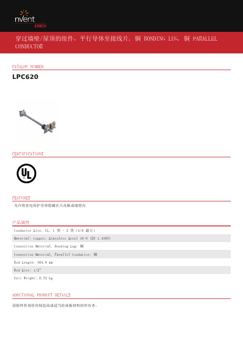
CATALOG NUMBERLPC620CERTIFICATIONSFEATURES允许将雷电保护导体隐藏在天花板或墙壁内产品属性Conductor Size, UL: 1 类 - 2 类(4/0 最大)Material: Copper; Stainless Steel 18-8 (EN 1.4305) Connection Material, Bonding Lug: 铜Connection Material, Parallel Conductor: 铜Rod Length: 304.8 mmRod Size: 1/2"Unit Weight: 0.72 kgADDITIONAL PRODUCT DETAILS请始终咨询屋顶制造商或适当防雨板材料的所有者。
DIAGRAMS警告应仅根据 nVent 的产品说明书与培训材料安装并使用 nVent 的产品。
可访问 获取说明书,或者向您的 nVent 客服代表索取。
错误安装、使用不当、滥用或未能完全遵守 nVent的说明与警告,可能会造成产品故障、财产损失、严重的人身伤害及死亡和/或使得保修服务无效。
北美+1.800.753.9221Option 1 – Customer Care Option 2 – Technical Support 欧洲Netherlands:+31 800-0200135France:+33 800 901 793欧洲Germany:800 1890272Other Countries:+31 13 5835404APACShanghai:+ 86 21 2412 1618/19Sydney:+61 2 9751 8500 CADDY ERICO HOFFMAN RAYCHEM SCHROFFTRACER2。
PHT6N06LT中文资料

gfs
Qg(tot) Qgs Qgd
Ciss Coss Crss
td on tr td off tf
Forward transconductance
Total gate charge Gate-source charge Gate-drain (Miller) charge
Junction temperature
Drain-source on-state
resistance
VGS = 5 V
MAX.
55 5.5 2.5 8.3 150 150
PINNING - SOT223
PIN
DESCRIPTION
1 gate
2 drain
3 source
4 drain (tab)
ESD LIMITING VALUE
SYMBOL VC
PARAMETER
Electrostatic discharge capacitor voltage
CONDITIONS
Human body model (100 pF, 1.5 kΩ)
MIN.
- 55
MAX.
55 55 ±13 5.5 2.5 3.8 1.75 22 10 8.3 1.8 150
Drain-source breakdown
VGS = 0 V; ID = 0.25 mA
voltage
Tj = -55˚C
Gate threshold voltage
VDS = VGS; ID = 1 mA
Tj = 150˚C
Tj = -55˚C
Zero gate voltage drain current VDS = 55 V; VGS = 0 V;
超特克 DSFP-VN0606 增强模式电源管说明书

Supertex inc.VN0606YY = Year Sealed WW = Week Sealed= “Green” PackagingSi VN 0606L YYWW Features►Free from secondary breakdown ►Low power drive requirement ►Ease of paralleling►Low C ISS and fast switching speeds ►Excellent thermal stability ►Integral source-drain diode►High input impedance and high gainApplications►Motor controls ►Converters ►Amplifiers ►Switches►Power supply circuits►Drivers (relays, hammers, solenoids, lamps, memories, displays, bipolar transistors, etc.)General DescriptionThis enhancement-mode (normally-off) transistor utilizes a vertical DMOS structure and Supertex’s well-proven, silicon-gate manufacturing process. This combination produces a device with the power handling capabilities of bipolar transistors and the high input impedance and positive temperature coefficient inherent in MOS devices. Characteristic of all MOS structures, this device is free from thermal runaway and thermally-induced secondary breakdown.Supertex’s vertical DMOS FETs are ideally suited to a wide range of switching and amplifying applications where very low threshold voltage, high breakdown voltage, high input impedance, low input capacitance, and fast switching speeds are desired.N-Channel Enhancement-ModeVertical DMOS FEToccur. Functional operation under these conditions is not implied. Continuous operation of the device at the absolute rating level may affect device reliability. All voltages are referenced to device ground.TO-92Product MarkingPackage may or may not include the following marks: Si orPin ConfigurationTO-92GATESOURCEDRAINContact factory for Wafer / Die availablity.Devices in Wafer / Die form are lead (Pb)-free / RoHS compliant.OSwitching Waveforms and Test CircuitOUTPUTINPUTOUTPUT10VVDD0V0V1. All D.C. parameters 100% tested at 25O C unless otherwise stated. (Pulse test: 300µs pulse, 2% duty cycle.)2. All A.C. parameters sample tested.† I D (continuous) is limited by max rated T j .Supertex inc. does not recommend the use of its products in life support applications, and will not knowingly sell them for use in such applications unless it receives an adequate “product liability indemnification insurance agreement.” Supertex inc. does not assume responsibility for use of devices described, and limits its liability to the replacement of the devices determined defective due to workmanship. No responsibility is assumed for possible omissions and inaccuracies. Circuitry and specifications are subject to change without notice. For the latest product specifications refer to the Supertex inc. (website: http//)©2013 Supertex inc. All rights reserved. Unauthorized use or reproduction is prohibited.Supertex inc.(The package drawing(s) in this data sheet may not reflect the most current specifications. For the latest package outline information go to /packaging.html .)3-Lead TO-92 Package Outline (L)JEDEC Registration TO-92.* This dimension is not specified in the JEDEC drawing.† This dimension differs from the JEDEC drawing.Drawings not to scale.Supertex Doc.#: DSPD-3TO92N3, Version E041009.。
NTD20N06L中文资料

NTD20N06LPower MOSFET20 Amps, 60 Volts, Logic LevelN−Channel DPAKDesigned for low voltage, high speed switching applications in power supplies, converters and power motor controls and bridge circuits.Typical Applications•Power Supplies •Converters•Power Motor Controls •Bridge CircuitsMAXIMUM RATINGS (T= 25°C unless otherwise noted)1.When surface mounted to an FR4 board using 1″ pad size,(Cu Area 1.127 in 2).2.When surface mounted to an FR4 board using recommended pad size,(Cu Area 0.412 in 2).Device Package Shipping ORDERING INFORMATIONNTD20N06L DPAK 75 Units/Rail NTD20N06L−1DPAK Straight Lead75 Units/RailNTD20N06LT4DPAK2500 Tape & ReelELECTRICAL CHARACTERISTICS(T = 25°C unless otherwise noted)4.Switching characteristics are independent of operating junction temperatures.21.61.21.410.80.620I D , D R A I N C U R R E N T (A M P S )0Figure 3. On−Resistance versusGate−to−Source VoltageI D , DRAIN CURRENT (AMPS)Figure 4. On−Resistance versus Drain Currentand Gate VoltageI D , DRAIN CURRENT (AMPS)R D R D S (o n ), D R A I N −T O −S O U R C E R E S I S T A N C E (Ω)Figure 5. On−Resistance Variation withTemperature T J , JUNCTION TEMPERATURE (°C)Figure 6. Drain−to−Source Leakage Currentversus VoltageV DS , DRAIN−TO−SOURCE VOLTAGE (VOLTS)R D S (o n ), D R A I N −T O −S O U R C E R E S I S T A N C E (N O R M A L I Z E D )40−505025−257512510040302060101015017530501.8POWER MOSFET SWITCHINGSwitching behavior is most easily modeled and predicted by recognizing that the power MOSFET is charge controlled. The lengths of various switching intervals (∆t)are determined by how fast the FET input capacitance can be charged by current from the generator.The published capacitance data is difficult to use for calculating rise and fall because drain−gate capacitance varies greatly with applied voltage. Accordingly, gate charge data is used. In most cases, a satisfactory estimate of average input current (I G(A V)) can be made from a rudimentary analysis of the drive circuit so that t = Q/I G(A V)During the rise and fall time interval when switching a resistive load, V GS remains virtually constant at a level known as the plateau voltage, V SGP . Therefore, rise and fall times may be approximated by the following:t r = Q 2 x R G /(V GG − V GSP )t f = Q 2 x R G /V GSP whereV GG = the gate drive voltage, which varies from zero to V GG R G = the gate drive resistanceand Q 2 and V GSP are read from the gate charge curve.During the turn−on and turn−off delay times, gate current is not constant. The simplest calculation uses appropriate values from the capacitance curves in a standard equation for voltage change in an RC network. The equations are:t d(on) = R G C iss In [V GG /(V GG − V GSP )]t d(off) = R G C iss In (V GG /V GSP )The capacitance (C iss ) is read from the capacitance curve at a voltage corresponding to the off−state condition when calculating t d(on) and is read at a voltage corresponding to the on−state when calculating t d(off).At high switching speeds, parasitic circuit elements complicate the analysis. The inductance of the MOSFET source lead, inside the package and in the circuit wiring which is common to both the drain and gate current paths,produces a voltage at the source which reduces the gate drive current. The voltage is determined by Ldi/dt, but since di/dt is a function of drain current, the mathematical solution is complex. The MOSFET output capacitance also complicates the mathematics. And finally, MOSFETs have finite internal gate resistance which effectively adds to the resistance of the driving source, but the internal resistance is difficult to measure and, consequently, is not specified.The resistive switching time variation versus gate resistance (Figure 9) shows how typical switching performance is affected by the parasitic circuit elements. If the parasitics were not present, the slope of the curves would maintain a value of unity regardless of the switching speed.The circuit used to obtain the data is constructed to minimize common inductance in the drain and gate circuit loops and is believed readily achievable with board mounted components. Most power electronic loads are inductive; the data in the figure is taken with a resistive load, which approximates an optimally snubbed inductive load. Power MOSFETs may be safely operated into an inductive load;however, snubbing reduces switching losses.GATE−TO−SOURCE OR DRAIN−TO−SOURCE VOLTAGE (VOLTS)C , C A P A C I T A N C E (p F )Figure 7. Capacitance VariationV SD , SOURCE−TO−DRAIN VOLTAGE (VOLTS)Figure 10. Diode Forward Voltage versus CurrentV G S , G A T E −T O −S O U R C E V O L T A G E (V O L T S )SAFE OPERATING AREAThe Forward Biased Safe Operating Area curves define the maximum simultaneous drain−to−source voltage and drain current that a transistor can handle safely when it is forward biased. Curves are based upon maximum peak junction temperature and a case temperature (T C ) of 25°C.Peak repetitive pulsed power limits are determined by using the thermal response data in conjunction with the procedures discussed in AN569, “Transient Thermal Resistance −General Data and Its Use.”Switching between the off−state and the on−state may traverse any load line provided neither rated peak current (I DM ) nor rated voltage (V DSS ) is exceeded and the transition time (t r ,t f ) do not exceed 10 µs. In addition the total power averaged over a complete switching cycle must not exceed (T J(MAX) − T C )/(R θJC ).A Power MOSFET designated E−FET can be safely used in switching circuits with unclamped inductive loads. Forreliable operation, the stored energy from circuit inductance dissipated in the transistor while in avalanche must be less than the rated limit and adjusted for operating conditions differing from those specified. Although industry practice is to rate in terms of energy, avalanche energy capability is not a constant. The energy rating decreases non−linearly with an increase of peak current in avalanche and peak junction temperature.Although many E−FETs can withstand the stress of drain−to−source avalanche at currents up to rated pulsed current (I DM ), the energy rating is specified at rated continuous current (I D ), in accordance with industry custom.The energy rating must be derated for temperature as shown in the accompanying graph (Figure 12). Maximum energy at currents below rated continuous I D can safely be assumed to equal the values indicated.SAFE OPERATING AREAFigure 13. Thermal Response1100I D , D R A I N C U R R E N T (A M P S )0.110Figure 14. Diode Reverse Recovery WaveformTIMEr (t ), E F F E C T I V E T R A N S I E N T T H E R M A L R E S I S T A N C E t, TIME (s)1100.10.010.0010.00010.00001INFORMATION FOR USING THE DPAK SURFACE MOUNT PACKAGE RECOMMENDED FOOTPRINT FOR SURFACE MOUNTED APPLICATIONSSurface mount board layout is a critical portion of the total design. The footprint for the semiconductor packages must be the correct size to ensure proper solder connection interface between the board and the package. With the correct pad geometry, the packages will self align when subjected to a solder reflow process.ǒmm inches ǓSCALE 3:1SOLDER STENCIL GUIDELINESPrior to placing surface mount components onto a printed circuit board, solder paste must be applied to the pads. Solder stencils are used to screen the optimum amount. These stencils are typically 0.008 inches thick and may be made of brass or stainless steel. For packages such as the SC−59, SC−70/SOT−323, SOD−123, SOT−23, SOT−143, SOT−223, SO−8, SO−14, SO−16, and SMB/SMC diode packages, the stencil opening should be the same as the pad size or a 1:1 registration. This is not the case with the DPAK and D2PAK packages. If one uses a 1:1 opening to screen solder onto the drain pad, misalignment and/or “tombstoning” may occur due to an excess of solder. For these two packages, the opening in the stencil for the paste should be approximately 50% of the tab area. The opening for the leads is still a 1:1 registration. Figure 15 shows a typical stencil for the DPAK and D2PAK packages. The pattern of the opening in the stencil for the drain pad is not critical as long as it allows approximately 50% of the pad to be covered with paste.Figure 15. Typical Stencil for DPAK andD2PAK PackagesSOLDER PASTEOPENINGSSTENCILSOLDERING PRECAUTIONSThe melting temperature of solder is higher than the rated temperature of the device. When the entire device is heated to a high temperature, failure to complete soldering within a short time could result in device failure. Therefore, the following items should always be observed in order to minimize the thermal stress to which the devices are subjected.•Always preheat the device.•The delta temperature between the preheat and soldering should be 100°C or less.*•When preheating and soldering, the temperature of the leads and the case must not exceed the maximum temperature ratings as shown on the data sheet. When using infrared heating with the reflow soldering method, the difference shall be a maximum of 10°C.•The soldering temperature and time shall not exceed 260°C for more than 10 seconds.•When shifting from preheating to soldering, the maximum temperature gradient shall be 5°C or less.•After soldering has been completed, the device should be allowed to cool naturally for at least three minutes.Gradual cooling should be used as the use of forced cooling will increase the temperature gradient and result in latent failure due to mechanical stress.•Mechanical stress or shock should not be applied during cooling.*Soldering a device without preheating can cause excessive thermal shock and stress which can result in damage to the device.*Due to shadowing and the inability to set the wave height to incorporate other surface mount components, the D2PAK is not recommended for wave soldering.TYPICAL SOLDER HEATING PROFILEFor any given circuit board, there will be a group of control settings that will give the desired heat pattern. The operator must set temperatures for several heating zones,and a figure for belt speed. Taken together, these control settings make up a heating “profile” for that particular circuit board. On machines controlled by a computer, the computer remembers these profiles from one operating session to the next. Figure 16 shows a typical heating profile for use when soldering a surface mount device to a printed circuit board. This profile will vary among soldering systems but it is a good starting point. Factors that can affect the profile include the type of soldering system in use, density and types of components on the board, type of solder used, and the type of board or substrate material being used. This profile shows temperature versus time.The line on the graph shows the actual temperature that might be experienced on the surface of a test board at or near a central solder joint. The two profiles are based on a high density and a low density board. The Vitronics SMD310 convection/infrared reflow soldering system was used to generate this profile. The type of solder used was 62/36/2 Tin Lead Silver with a melting point between 177−189°C. When this type of furnace is used for solder reflow work, the circuit boards and solder joints tend to heat first. The components on the board are then heated by conduction. The circuit board, because it has a large surface area, absorbs the thermal energy more efficiently, then distributes this energy to the components. Because of this effect, the main body of a component may be up to 30degrees cooler than the adjacent solder joint.STEP 1PREHEAT ZONE 1STEP 2VENT “SOAK”STEP 3HEATING ZONES 2 & 5STEP 4HEATING ZONES 3 & 6STEP 5HEATING ZONES 4 & 7STEP 6VENT STEP 7COOLING 200°150°100°5°°C Figure 16. Typical Solder Heating ProfilePACKAGE DIMENSIONSDPAKCASE 369C−01ISSUE OVSDIM MIN MAX MIN MAX MILLIMETERSINCHES A 0.2350.245 5.97 6.22B 0.2500.265 6.35 6.73C 0.0860.094 2.19 2.38D 0.0270.0350.690.88E 0.0180.0230.460.58F 0.0370.0450.94 1.14G 0.180 BSC 4.58 BSC H 0.0340.0400.87 1.01J 0.0180.0230.460.58K 0.1020.114 2.60 2.89L 0.090 BSC 2.29 BSC R 0.1800.215 4.57 5.45S 0.0250.0400.63 1.01U 0.020−−−0.51−−−V 0.0350.0500.89 1.27Z0.155−−−3.93−−−STYLE 2:PIN 1.GATE2.DRAIN3.SOURCE4.DRAINDPAKCASE 369D−01ISSUE OENOTES:1.DIMENSIONING AND TOLERANCING PER ANSI Y14.5M, 1982.STYLE 2:PIN 1.GATE2.DRAIN3.SOURCE4.DRAINNotes11ON Semiconductor and are registered trademarks of Semiconductor Components Industries, LLC (SCILLC). SCILLC reserves the right to make changes without further notice to any products herein. SCILLC makes no warranty, representation or guarantee regarding the suitability of its products for any particular purpose, nor does SCILLC assume any liability arising out of the application or use of any product or circuit, and specifically disclaims any and all liability, including without limitation special, consequential or incidental damages. “Typical” parameters which may be provided in SCILLC data sheets and/or specifications can and do vary in different applications and actual performance may vary over time. All operating parameters, including “Typicals” must be validated for each customer application by customer’s technical experts. SCILLC does not convey any license under its patent rights nor the rights of others.SCILLC products are not designed, intended, or authorized for use as components in systems intended for surgical implant into the body, or other applications intended to support or sustain life, or for any other application in which the failure of the SCILLC product could create a situation where personal injury or death may occur. Should Buyer purchase or use SCILLC products for any such unintended or unauthorized application, Buyer shall indemnify and hold SCILLC and its officers, employees, subsidiaries, affiliates, and distributors harmless against all claims, costs, damages, and expenses, and reasonable attorney fees arising out of, directly or indirectly, any claim of personal injury or death associated with such unintended or unauthorized use, even if such claim alleges that SCILLC was negligent regarding the design or manufacture of the part. SCILLC is an Equal Opportunity/Affirmative Action Employer. PUBLICATION ORDERING INFORMATIONJAPAN: ON Semiconductor, Japan Customer Focus Center2−9−1 Kamimeguro, Meguro−ku, Tokyo, Japan 153−0051Phone: 81−3−5773−3850。
FAIRCHILD FQPF20N06 60V N-Channel MOSFET 说明书

现货库存、技术资料、百科信息、热点资讯,精彩尽在鼎好!FQPF20N06TO-220FG SDNotes:1. Repetitive Rating : Pulse width limited by maximum junction temperature2. L = 800µH, I AS = 15A, V DD = 25V, R G = 25 Ω, Starting T J = 25°C3. I SD ≤ 20A, di/dt ≤ 300A/µs, V DD ≤ BV DSS, Starting T J = 25°C4. Pulse Test : Pulse width ≤300µs, Duty cycle ≤2%5. Essentially independent of operating temperature∆BV DSS / ∆T J Breakdown Voltage Temperature CoefficientI D = 250 µA, Referenced to 25°C --0.07--V/°C I DSS Zero Gate Voltage Drain Current V DS = 60 V, V GS = 0 V ----1µA V DS = 48 V, T C = 150°C ----10µA I GSSF Gate-Body Leakage Current, Forward V GS = 25 V, V DS = 0 V ----100nA I GSSRGate-Body Leakage Current, ReverseV GS = -25 V, V DS = 0 V-----100nAOn CharacteristicsV GS(th)Gate Threshold Voltage V DS = V GS , I D = 250 µA2.0-- 4.0V R DS(on)Static Drain-Source On-ResistanceV GS = 10 V, I D = 7.5 A --0.0480.06Ωg FSForward TransconductanceV DS = 25 V, I D = 7.5 A --10--SDynamic CharacteristicsC iss Input Capacitance V DS = 25 V, V GS = 0 V, f = 1.0 MHz--450590pF C oss Output Capacitance--170220pF C rssReverse Transfer Capacitance--2535pFSwitching Characteristicst d(on)Turn-On Delay Time V DD = 30 V, I D = 10 A,R G = 25 Ω--520ns t r Turn-On Rise Time --45100ns t d(off)Turn-Off Delay Time --2050ns t f Turn-Off Fall Time --2560ns Q g Total Gate Charge V DS = 48 V, I D = 20 A,V GS = 10 V--11.515nC Q gs Gate-Source Charge --3--nC Q gdGate-Drain Charge--4.5--nCDrain-Source Diode Characteristics and Maximum RatingsI S Maximum Continuous Drain-Source Diode Forward Current ----15A I SM Maximum Pulsed Drain-Source Diode Forward Current----60A V SD Drain-Source Diode Forward Voltage V GS = 0 V, I S = 15 A ---- 1.5V t rr Reverse Recovery Time V GS = 0 V, I S = 20 A,dI F / dt = 100 A/µs --43--ns Q rrReverse Recovery Charge--50--nC(Note 4)(Note 4, 5)(Note 4, 5)(Note 4)TRADEMARKSThe following are registered and unregistered trademarks Fairchild Semiconductor owns or is authorized to use and is not intended to be an exhaustive list of all such trademarks.DISCLAIMERFAIRCHILD SEMICONDUCTOR RESERVES THE RIGHT TO MAKE CHANGES WITHOUT FURTHER NOTICE TO ANY PRODUCTS HEREIN TO IMPROVE RELIABILITY, FUNCTION OR DESIGN. FAIRCHILD DOES NOT ASSUME ANY LIABILITY ARISING OUT OF THE APPLICATION OR USE OF ANY PRODUCT OR CIRCUIT DESCRIBED HEREIN;NEITHER DOES IT CONVEY ANY LICENSE UNDER ITS PATENT RIGHTS, NOR THE RIGHTS OF OTHERS.LIFE SUPPORT POLICYFAIRCHILD’S PRODUCTS ARE NOT AUTHORIZED FOR USE AS CRITICAL COMPONENTS IN LIFE SUPPORT DEVICES OR SYSTEMS WITHOUT THE EXPRESS WRITTEN APPROVAL OF FAIRCHILD SEMICONDUCTOR CORPORATION.As used herein:1. Life support devices or systems are devices or systems which, (a) are intended for surgical implant into the body,or (b) support or sustain life, or (c) whose failure to perform when properly used in accordance with instructions for use provided in the labeling, can be reasonably expected to result in significant injury to the user.2. A critical component is any component of a life support device or system whose failure to perform can be reasonably expected to cause the failure of the life support device or system, or to affect its safety or effectiveness.PRODUCT STATUS DEFINITIONS Definition of TermsDatasheet Identification Product Status DefinitionAdvance InformationFormative or In Design This datasheet contains the design specifications for product development. Specifications may change in any manner without notice.PreliminaryFirst ProductionThis datasheet contains preliminary data, andsupplementary data will be published at a later date.Fairchild Semiconductor reserves the right to make changes at any time without notice in order to improve design.No Identification Needed Full ProductionThis datasheet contains final specifications. Fairchild Semiconductor reserves the right to make changes at any time without notice in order to improve design.Obsolete Not In ProductionThis datasheet contains specifications on a product that has been discontinued by Fairchild semiconductor.The datasheet is printed for reference information only.ACEx™Bottomless™CoolFET™CROSSVOLT™DenseTrench™DOME™EcoSPARK™E 2CMOS™EnSigna™FACT™FACT Quiet Series™FAST ®FASTr™FRFET™GlobalOptoisolator™GTO™HiSeC™ISOPLANAR™LittleFET™MicroFET™MICROWIRE™OPTOLOGIC™OPTOPLANAR™PACMAN ™POP™PowerTrench ®QFET™QS™QT Optoelectronics™Quiet Series™SLIENT SWITCHER ®SMART START™Stealth™SuperSOT™-3SuperSOT™-6SuperSOT™-8SyncFET™TinyLogic™UHC™UltraFET ®VCX™。
X02xxxN中文资料
Sensitivity
02
03
05
20
20
200
200
50
0.8
0.1
8 0.5
5
6
1.5
5
200
15
20
15
100
Fig.8 : On-state characteristics (maximum values).
I TSM (A). I2 t (A2 s) 100
ITSM 10
I2 t
1 1
Tj initial = 25oC
tp(ms) 10
I TM (A) 100
Tj initial 25oC
10
Tj max
The ST logo is a trademark of STMicroelectronics
VD=67%VDRM RGK = 1 KΩ
ITM= 3 x IT(AV) VR=35V dI/dt=10A/µs tp=100µs dV/dt=2V/µs VD= 67%VDRM RGK = 1 KΩ
Tj= 25°C MIN MAX
Tj= 25°C MAX Tj= 125°C MIN
Tj= 25°C MIN Tj= 25°C TYP
0.8
= 180o
0.6
0.4
0.2 0.0
0
Ttab (oC) 10 20 30 40 50 60 70 80 90 100 110 120 130
Fig.4 : Relative variation of thermal impedance junction to ambient versus pulse duration.
20mnv6 标准

20mnv6 标准20MnV6是一种低合金马氏体淬火和回火钢,主要用于制造机械零部件,如轴承、销轴、螺栓和连接杆等。
它具有良好的强度和韧性,适用于高应力和高负荷的工作环境。
20MnV6钢的化学成分包括碳(C)、硅(Si)、锰(Mn)、钒(V)和铬(Cr)等元素。
其中,碳的含量较低,使得钢具有良好的焊接性能和冷变形性能;硅的添加提高了钢的强度和硬度;锰的含量增加了钢的韧性和可焊性;钒的加入提高了钢的强度和耐磨性;铬的含量有助于提高钢的耐腐蚀性能。
20MnV6钢的热处理工艺是其性能优良的关键。
一般情况下,该钢材经过正火、淬火和回火等工艺处理,以达到所需的硬度、强度和韧性。
正火可以改善钢材的加工硬度和可加工性;淬火可以提高钢材的硬度和强度;回火则可以降低钢材的脆性,提高其韧性和抗冲击性。
20MnV6钢的标准规定了其化学成分、机械性能、热处理工艺等方面的要求。
在生产和加工过程中,必须严格按照标准的要求进行,以确保钢材的质量和性能达到标准规定的要求。
在使用20MnV6钢材制造零部件时,需要根据实际工作条件和要求选择合适的热处理工艺和工艺参数,以确保所制造的零部件具有良好的性能和可靠的使用寿命。
同时,还需要对钢材的质量进行严格的控制和检测,以排除可能存在的缺陷和问题,确保零部件的质量和可靠性。
总的来说,20MnV6标准钢材具有良好的强度、韧性和耐磨性,适用于制造高负荷和高应力下工作的零部件。
在生产和加工过程中,必须严格按照标准规定的要求进行,以确保钢材的质量和性能达到标准规定的要求。
同时,在使用过程中,需要根据实际工作条件和要求选择合适的热处理工艺和工艺参数,对钢材的质量进行严格的控制和检测,以确保制造的零部件具有良好的性能和可靠的使用寿命。
FGB20N6S2T中文资料

பைடு நூலகம்
Features
• 100kHz Operation at 390V, 7A • 200kHZ Operation at 390V, 5A • 600V Switching SOA Capability • Typical Fall Time . . . . . . . . . . 85ns at TJ = 125oC • Low Gate Charge . . . . . . . . . 30nC at VGE = 15V • Low Plateau Voltage . . . . . . . . . . . . . 6.5V Typical • UIS Rated . . . . . . . . . . . . . . . . . . . . . . . . . 100mJ • Low Conduction Loss • Low Eon
Symbol BVCES IC25 IC110 ICM VGES VGEM SSOA EAS EARV PD TJ TSTG Parameter Collector to Emitter Breakdown Voltage Collector Current Continuous, TC = 25°C Collector Current Continuous, TC = 110°C Collector Current Pulsed (Note 1) Gate to Emitter Voltage Continuous Gate to Emitter Voltage Pulsed Switching Safe Operating Area at TJ = 150°C, Figure 2 Pulsed Avalanche Energy, ICE = 7.0A, L = 4mH, VDD = 50V Pulsed Avalanche Energy, ICE = 7.0A, L = 4mH, VDD = 50V Power Dissipation Total TC = 25°C Power Dissipation Derating TC > 25°C Operating Junction Temperature Range Storage Junction Temperature Range Ratings 600 28 13 40 ±20 ±30 35 at 600V 100 100 125 1.0 -55 to 150 -55 to 150 Units V A A A V V A mJ mJ W W/°C °C °C
- 1、下载文档前请自行甄别文档内容的完整性,平台不提供额外的编辑、内容补充、找答案等附加服务。
- 2、"仅部分预览"的文档,不可在线预览部分如存在完整性等问题,可反馈申请退款(可完整预览的文档不适用该条件!)。
- 3、如文档侵犯您的权益,请联系客服反馈,我们会尽快为您处理(人工客服工作时间:9:00-18:30)。
PHX20N06TN-channel TrenchMOS™ standard level FETRev. 01 — 16 February 2004Product data1.Product profile1.1DescriptionN-channel enhancement mode field-effect power transistor in a fully isolated plastic package using T renchMOS™ technology.1.2Features1.3Applications1.4Quick reference data2.Pinning informations Standard level compatibles Isolated package.s DC motor control s Synchronous rectifications DC-to-DC converterss General purpose power switching.s V DS ≤55V s I D ≤12.9As P tot ≤23Ws R DSon ≤75m Ω.Table 1:Pinning - SOT186A (TO-220F), simplified outline and symbolPin Description Simplified outline Symbol1gate (g)SOT186A (TO-220F)2source (s)3drain (d)mbmounting base;isolatedMBK1101mb23sdgMBB076M3D3083.Ordering information4.Limiting values[1]External heatsink connected to mounting base.Table 2:Ordering informationType numberPackage NameDescriptionVersionPHX20N06TTO-220FPlastic single-ended package;isolated heatsink mounted;1mounting hole;3 lead TO-220 ‘full pack’SOT186A Table 3:Limiting valuesIn accordance with the Absolute Maximum Rating System (IEC 60134).Symbol Parameter Conditions Min Max Unit V DS drain-source voltage (DC)25°C ≤T j ≤150°C-55V V DGR drain-gate voltage (DC)25°C ≤T j ≤150°C; R GS =20k Ω-55V V GS gate-source voltage (DC)-±20V I D drain current (DC)T h =25°C; V GS =10V;Figure 2and 3[1]-12.9A T h =100°C; V GS =10V;Figure 2[1]-8.1A I DM peak drain current T h =25°C; pulsed; t p ≤10µs;Figure 3[1]51.6A P tot total power dissipation T h =25°C;Figure 1[1]-23W T stg storage temperature −55+150°C T j junction temperature−55+150°C Source-drain diodeI S source (diode forward) current (DC)T h =25°C[1]-12.9A I SMpeak source (diode forward) current T h =25°C; pulsed; t p ≤10µs[1]-51.6A Avalanche ruggednessE DS(AL)S non-repetitive drain-sourceavalanche energyunclamped inductive load; I D =11A;t p =0.06ms; V DD ≤15V; R GS =50Ω;V GS =10V; starting T j =25°C-30.3mJV GS ≥10VFig 1.Normalized total power dissipation as afunction of heatsink temperature.Fig 2.Normalized continuous drain current as afunction of heatsink temperature.T h =25°C; I DM is single pulse.Fig 3.Safe operating area; continuous and peak drain currents as a function of drain-source voltage.03aa134080120050100150T h (°C)P der (%)03aa214080120050100150200T h (°C)I der (%)P der P totP tot 25C °()-----------------------100%×=I der I DI D 25C °()-------------------100%×=03am7010-1110102 110102V DS (V)I D (A)DC100 µs10 ms1 ms t p = 10 µsLimit R DSon = V DS / I D5.Thermal characteristics[1]External heatsink connected to mounting base.5.1Transient thermal impedanceTable 4:Thermal characteristicsSymbol ParameterConditions Min Typ Max Unit R th(j-h)thermal resistance from junction to heatsink.Figure 4[1]-- 5.4K/W R th(j-a)thermal resistance from junction to ambient.vertical in still air-55-K/WFig 4.Transient thermal impedance from junction to heatsink as a function of pulse duration.03am6910-111010-510-410-310-210-1110t p (s)Z th(j-h)(K/W)single pulseδ = 0.50.20.10.050.02t pt p TPtTδ =6.CharacteristicsTable 5:CharacteristicsT j=25°C unless otherwise specified.Symbol Parameter Conditions Min Typ Max Unit Static characteristicsV(BR)DSS drain-source breakdown voltage I D=0.25mA; V GS=0VT j=25°C55--VT j=−55°C50--VV GS(th)gate-source threshold voltage I D=1mA; V DS=V GS;Figure9T j=25°C234VT j=150°C 1.2--VT j=−55°C-- 4.4VI DSS drain-source leakage current V DS=55V; V GS=0VT j=25°C-0.0510µAT j=150°C--500µA I GSS gate-source leakage current V GS=±20V; V DS=0V-2100nA R DSon drain-source on-state resistance V GS=10V; I D=10A;Figure7and8T j=25°C-5075mΩT j=150°C-75138mΩDynamic characteristicsQ g(tot)total gate charge I D=10A; V DD=44V; V GS=10V;Figure13-9.8-nC Q gs gate-source charge- 2.2-nC Q gd gate-drain (Miller) charge- 4.7-nC C iss input capacitance V GS=0V; V DS=25V; f=1MHz;Figure11-320-pF C oss output capacitance-90-pF C rss reverse transfer capacitance-60-pFt d(on)turn-on delay time V DD=30V; R L=1.2Ω;V GS=10V;R G=10Ω;-10-nst r rise time-50-ns t d(off)turn-off delay time-70-ns t f fall time-40-ns Source-drain diodeV SD source-drain (diode forward) voltage I S=15A; V GS=0V; Figure12- 1.02 1.2Vt rr reverse recovery time I S=20A; dI S/dt=−100A/µs;V GS=−10V;V DS=30V -32-nsQ r recovered charge-120-nCT j =25°C T j =25°C and 150°C; V DS >I D ×R DSonFig 5.Output characteristics: drain current as afunction of drain-source voltage;typical values.Fig 6.Transfer characteristics: drain current as afunction of gate-source voltage; typical valuesT j =25°CFig 7.Drain-source on-state resistance as a functionof drain current; typical values.Fig 8.Normalized drain source on-state resistance factor as a function of junction temperature.03am710510150.511.52V DS (V)I D (A)T j = 25 °CV GS = 4.2 V10 V 4.6 V5 V7 V 6.5 V6 V 5.8 V5.4 V03am7305101502468V GS (V)I D (A)V DS > I D x R DSonT j = 25 °C150 °C03am720255075100051015I D (A)R DSon (m Ω)V GS = 6 VT j = 25 °C10 V7 V6.5 V 03aa2800.61.21.82.4-6060120180aT j (°C)a RDSon R DSon 25C °()----------------------------=I D =1mA; V DS =V GS T j =25°C; V DS =V GSFig 9.Gate-source threshold voltage as a function ofjunction temperature.Fig 10.Sub-threshold drain current as a function ofgate-source voltage.V GS =0V; f =1MHzFig 11.Input, output and reverse transfer capacitances as a function of drain-source voltage; typical values.03aa32012345-6060120180T j (°C)V GS(th) (V)maxmintyp03aa3510-610-510-410-310-210-10246V GS (V)I D (A)maxtyp min 03am751010210310-11 10102V DS (V)C (pF)C issC oss C rss7.Isolation characteristicsV GS =0V I D =10A; V DD =14V and 44VFig 12.Reverse diode current as a function of reversediode voltage; typical values.Fig 13.Gate-source voltage as a function of turn-ongate charge; typical values.03am740510150.30.60.91.2V SD (V)I S (A)T j = 25 °C150 °CV GS = 0 V03am7602468100246810Q G (nC)V GS (V)I D = 10 A T j = 25 °CV DD = 14 V44 VTable 6:Isolation characteristics SymbolParameterConditionsMin.Typ.Max.Unit V (isol)RMS RMS isolation voltage from all threeterminals to external heatsink f =50-60Hz; sinusoidal waveform;RH ≤65%; clean and dust-free.--2500V C (d-h)Capacitance from drain to external heatsink-10-pF8.Package outlineFig 14.SOT186A (TO-220F).REFERENCESOUTLINE VERSION EUROPEAN PROJECTIONISSUE DATE IECJEDEC JEITASOT186A3-lead TO-220F0510 mmscalePlastic single-ended package; isolated heatsink mounted;1 mounting hole; 3 lead TO-220 'full pack'SOT186AA A 1QcKjNotes1. Terminal dimensions within this zone are uncontrolled. Terminals in this zone are not tinned.2. Both recesses are ∅ 2.5 × 0.8 max. depthDD 1LL 2L 1b 1b 2e 1e b w M123qE PTUNIT D b 1D 1e q Q P Lc L 2(1)max.e 1A 5.083mm 4.64.0A 12.92.5b 0.90.71.10.9b 21.41.00.70.415.815.26.56.3E 10.39.72.5414.413.5T(2)2.50.4L 13.302.79j 2.71.7K 0.60.42.62.33.02.6w 3.23.0DIMENSIONS (mm are the original dimensions)02-03-1202-04-09mounting base9.Revision historyTable 7:Revision historyRev Date CPCN Description0120040216-Product data (9397 750 12834).9397 750 12834© Koninklijke Philips Electronics N.V . 2004. All rights reserved.Product data Rev. 01 — 16 February 200411 of 12Contact informationFor additional information, please visit .For sales office addresses, send e-mail to:sales.addresses@ .Fax: +31 40 27 2482510.Data sheet status[1]Please consult the most recently issued data sheet before initiating or completing a design.[2]The product status of the device(s) described in this data sheet may have changed since this data sheet was published. The latest information is available on the Internet at URL .[3]For data sheets describing multiple type numbers, the highest-level product status determines the data sheet status.11.DefinitionsShort-form specification —The data in a short-form specification is extracted from a full data sheet with the same type number and title. For detailed information see the relevant data sheet or data handbook.Limiting values definition — Limiting values given are in accordance with the Absolute Maximum Rating System (IEC 60134). Stress above one or more of the limiting values may cause permanent damage to the device.These are stress ratings only and operation of the device at these or at any other conditions above those given in the Characteristics sections of the specification is not implied. Exposure to limiting values for extended periods may affect device reliability.Application information — Applications that are described herein for any of these products are for illustrative purposes only. Philips Semiconductors make no representation or warranty that such applications will be suitable for the specified use without further testing or modification.12.DisclaimersLife support —These products are not designed for use in life support appliances, devices, or systems where malfunction of these products can reasonably be expected to result in personal injury. Philips Semiconductorscustomers using or selling these products for use in such applications do so at their own risk and agree to fully indemnify Philips Semiconductors for any damages resulting from such application.Right to make changes —Philips Semiconductors reserves the right to make changes in the products - including circuits, standard cells, and/or software - described or contained herein in order to improve design and/or performance. When the product is in full production (status ‘Production’),relevant changes will be communicated via a Customer Product/Process Change Notification (CPCN). Philips Semiconductors assumes noresponsibility or liability for the use of any of these products, conveys no licence or title under any patent, copyright, or mask work right to theseproducts,and makes no representations or warranties that these products are free from patent,copyright,or mask work right infringement,unless otherwise specified.13.TrademarksTrenchMOS —is a trademark of Koninklijke Philips Electronics N.V .Level Data sheet status [1]Product status [2][3]DefinitionI Objective data Development This data sheet contains data from the objective specification for product development. Philips Semiconductors reserves the right to change the specification in any manner without notice.IIPreliminary dataQualificationThis data sheet contains data from the preliminary specification.Supplementary data will be published at a later date.Philips Semiconductors reserves the right to change the specification without notice,in order to improve the design and supply the best possible product.III Product data ProductionThis data sheet contains data from the product specification. Philips Semiconductors reserves the right to make changes at any time in order to improve the design,manufacturing and supply.Relevant changes will be communicated via a Customer Product/Process Change Notification (CPCN).© Koninklijke Philips Electronics N.V .2004.Printed in The NetherlandsAll rights are reserved.Reproduction in whole or in part is prohibited without the prior written consent of the copyright owner.The information presented in this document does not form part of any quotation or contract,is believed to be accurate and reliable and may be changed without notice.No liability will be accepted by the publisher for any consequence of its use.Publication thereof does not convey nor imply any license under patent-or other industrial or intellectual property rights.Date of release: 16 February 2004Document order number: 9397 750 12834Contents1Product profile . . . . . . . . . . . . . . . . . . . . . . . . . . 11.1Description . . . . . . . . . . . . . . . . . . . . . . . . . . . . 11.2Features . . . . . . . . . . . . . . . . . . . . . . . . . . . . . . 11.3Applications . . . . . . . . . . . . . . . . . . . . . . . . . . . 11.4Quick reference data. . . . . . . . . . . . . . . . . . . . . 12Pinning information. . . . . . . . . . . . . . . . . . . . . . 13Ordering information. . . . . . . . . . . . . . . . . . . . . 24Limiting values. . . . . . . . . . . . . . . . . . . . . . . . . . 25Thermal characteristics. . . . . . . . . . . . . . . . . . . 45.1T ransient thermal impedance . . . . . . . . . . . . . . 46Characteristics. . . . . . . . . . . . . . . . . . . . . . . . . . 57Isolation characteristics . . . . . . . . . . . . . . . . . . 88Package outline . . . . . . . . . . . . . . . . . . . . . . . . . 99Revision history. . . . . . . . . . . . . . . . . . . . . . . . 1010Data sheet status. . . . . . . . . . . . . . . . . . . . . . . 1111Definitions . . . . . . . . . . . . . . . . . . . . . . . . . . . . 1112Disclaimers. . . . . . . . . . . . . . . . . . . . . . . . . . . . 1113Trademarks. . . . . . . . . . . . . . . . . . . . . . . . . . . . 11。