R09P05S中文资料
PQ05RD21中文资料

PQ05RD21 series Low Power-Loss Voltage Regulator
2.0A Output Type, High Cost Performance Low Power-Loss Voltage Regulator
General Description Sharp's PQ05RD21 series is 2.0A output type low power-loss voltage regulator(TO-220). It contributes to energy and space saving of various electronic equipment such as AV, OA equipment.
1
Input
Specific IC 3 GND
2
Output
4 ON/OFF control terminal
Model Line-up 2.0A output
3.3V output 5.0V output 9.0V output 12.0V output
PQ3RD23 PQ05RD21 PQ09RD21 PQ12RD21
*6 Input voltage shall be the value when output voltage is 95% in comparison with the initial value. PQ3RD23:Vin=3.7V *7 In case of opening control teminal 4 , output voltage turns on.
(Internet)
• Data for Sharp's optoelectronic/power devices is provided for internet. ( Address http://www.sharp.co.jp/ecg/)
R05P23.3D中文资料
15.000 10.000 5.000 0.000 -5.000 -10.000
R12P209S
Deviation from Nominal (%)
R05P205S R05P209S
15.000 10.000 5.000 0.000 -5.000 -10.000
R12P212S
R05P212S R05P212S
RxxP2xxS_D Series
3rd angle projection
7 PIN SIP Package
9.80
RECOM R05P205D **** Dual Output RECOM R05P205D ****
Single Output RECOM R05P205S ****
12.50
0.51
Safe Operating Area
85 Operating Temperature °C
64
July-2006
元器件交易网
ECONOLINE
DC/DC-Converter
RxxP2xxS_D Series
2113 x 103 hours 2434 x 103 hours 299 x 103 hours 334 x 103 hours
RxxP212/15D
Efficiency / Load
100 80 60 40
R12P212D R12P215D R05P215D R05P212D
Efficiency %
Efficiency %
20 0
20 0
0%
20%
40%
60%
80%
100%
0%
20%
40%
60%
RI-0905SP资料
0% 20% 40% 60% Total Output current (%)
80%
100%
0% 20% 40% 60% Total Output current (%)
80%
100%
RI-xx12S
Efficiency / Load
100 80 60 40 100
RI-xx15S
Efficiency / Load 0515
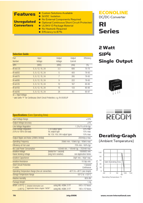
Input Voltage Range Output Voltage Accuracy Line Voltage Regulation Load Voltage Regulation (10% to 100% full load) Output Ripple and Noise (20MHz limited) Operating Frequency Efficiency at Full Load No Load Power Consumption Isolation Voltage Rated Working Voltage Isolation Capacitance Isolation Resistance Short Circuit Protection P-Suffix Operating Temperature Range (free air convection) Storage Temperature Range Relative Humidity Package Weight MTBF (+25°C) (+85°C) 70 3.3V output types 5V, output type 9V, 12V, 15V, 24V output types ±10% ±5% 1.2%/1% of Vin typ. 20% max. 15% max. 10% max. 200mVp-p max. 35kHz min. / 50kHz typ. / 85kHz max. 70% min. / 80% typ. 142mW min. / 185mW typ. / 252mW max. (tested for 1 second) 1000VDC min. (long term isolation) see Application Notes 30pF min. / 85pF max.
PQ05RF1_01中文资料

Unit
V
% % %/˚C dB V V µA V mA mA
V
❇3 PQ05RF1 series:VIN=7V, PQ09RF1 seris:VIN=15V, PQ12RF1 seris:VIN=18V ❇4 PQ05RF1/PQ05RF11/PQ05RF1V:VIN=6 to 12V
OFF-state current for control PQ05RF1/PQ05RF11 series
Quiescent current
Output voltage minute adjustment characteristics
PQ05RF1V PQ09RF1V PQ12RF1V
Symbol
Overheat protection circuit
3 •Please refer to the chapter " Handling Precautions ".
Notice In the absence of confirmation by device specification sheets,SHARP takes no responsibility for any defects that may occur in equipment using any SHARP devices shown in catalogs,data books,etc.Contact SHARP in order to obtain the latest device specification sheets before using any SHARP device.
元器件Lo交w P易o网wewr-wLwos.cseVcbo2ltba.gcoemRegulators
RPNS090AA1A11X资料
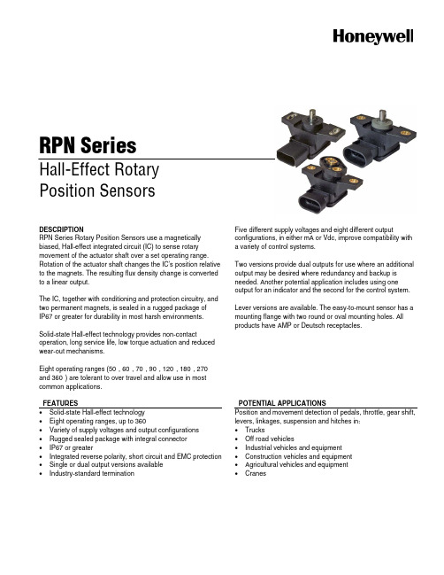
RPN SeriesHall-Effect Rotary Position SensorsDESCRIPTION RPN Series Rotary Position Sensors use a magnetically biased, Hall-effect integrated circuit (IC) to sense rotary movement of the actuator shaft over a set operating range. Rotation of the actuator shaft changes the IC’s position relative to the magnets. The resulting flux density change is converted to a linear output. The IC, together with conditioning and protection circuitry, and two permanent magnets, is sealed in a rugged package of IP67 or greater for durability in most harsh environments. Solid-state Hall-effect technology provides non-contact operation, long service life, low torque actuation and reduced wear-out mechanisms. Eight operating ranges (50°, 60°, 70°, 90°, 120°, 180°, 270° and 360°) are tolerant to over travel and allow use in most common applications. FEATURES • Solid-state Hall-effect technology • Eight operating ranges, up to 360° • Variety of supply voltages and output configurations • Rugged sealed package with integral connector • IP67 or greater • Integrated reverse polarity, short circuit and EMC protection • Single or dual output versions available • Industry-standard termination POTENTIAL APPLICATIONS Position and movement detection of pedals, throttle, gear shift, levers, linkages, suspension and hitches in: • Trucks • Off road vehicles • Industrial vehicles and equipment • Construction vehicles and equipment • Agricultural vehicles and equipment • Cranes Five different supply voltages and eight different output configurations, in either mA or Vdc, improve compatibility with a variety of control systems. Two versions provide dual outputs for use where an additional output may be desired where redundancy and backup is needed. Another potential application includes using one output for an indicator and the second for the control system. Lever versions are available. The easy-to-mount sensor has a mounting flange with two round or oval mounting holes. All products have AMP or Deutsch receptacles.RPN SeriesTable 1. RPNR Redundant (Dual) Output Specifications Characteristic Parameter Operating ranges available 50° (±25°), 90° (±45°) Output available 50° (±25°): Channel 1: 4 mA (left), 20 mA (right); Channel 2: 0.5 Vdc (left), 4.75 Vdc (right) 90° (±45°): Channel 1: 0.25 Vdc (left), 4.75 Vdc (right); Channel 2: 4.75 Vdc (left), 0.25 Vdc (right) Supply voltage range(s) 50° (±25°): Channel 1: 8.5 Vdc; Channel 2: 5 Vdc available 90° (±45°): Channel 1: 10 Vdc to 30 Vdc; Channel 2: 10 Vdc to 30 Vdc Current consumption 20 mA max. Output signal delay 3 ms approx. Accuracy ±1.6% Hysteresis none Linearity RPNR050SDMEC3A21X ±0.35° RPNR090KAAA3A11X ±0.6° Reverse polarity protection yes Operating and storage -40 °C to 125 °C [-40 °F to 257 °F] temperature range EMC 200 V/m ISO 11452-3 6 Expected life 30x10 cycles Protection class IP69K DIN 40050 Housing material PA66 plastic Shaft material stainless steel Termination AMP 1-1419168-1 Mechanical end stop no Table 2. RPNS Single Output Specifications Characteristic Operating ranges available Outputs availableSupply voltage range(s) available Current consumption (maximum) Output signal delay (approx) Reverse polarity protection EMC Operating and storage temperature range Protection class Accuracy Hysteresis Linearity RPNS050BB1A21X, RPNS050FA1A21X RPNS060AC1A21X RPNS070DD1A21X All other listings RPNS120AA1A21X Housing material Shaft material Expected life Termination Mechanical end stopParameter 50° (±25°), 60° (±30), 70° (±35), 90° (±45), 120° (±60), 180° (±90), 270° (±135), 360° (±180) 0.25 Vdc (left), 4.75 Vdc (right) 4 mA (left), 20 mA (right) 0.5 Vdc (left), 4.5 Vdc (right) 20 mA (left), 4 mA (right) 1 Vdc (left), 9 Vdc (right) 3 Vdc (left), 5 Vdc (right) 4.5 Vdc (left), 0.5 Vdc (right) 4.75 Vdc (left), 0.25 Vdc (right) 5 Vdc, 8 Vdc to 30 Vdc, 10 Vdc to 30 Vdc 20 mA 3 ms yes 200 V/m ISO 11452-3 -40 °C to 125 °C [-40 °F to 257 °F] IP67 DIN 40050 ±1.6% none ±0.35° ±0.6 ±1° ±2° ±5° PA66 plastic stainless steel 6 30x10 cycles AMP Superseal 282087-1, Deutsch DT04-3P no2/sensingHall-Effect Rotary Position SensorsFigure 1. RPNR Redundant (Dual) Output Versions (For Reference Only: mm/[in].) RPNR050DMEC3A21X RPNR090KAAA3A11XRFigure 2. RPNS Single Output Versions (For Reference Only: mm/[in].) RPNS050BB1A21X RPNS050FA1A21XReceptacle: AMP Superseal 282087-1 Mating Connector: AMP Superseal 282103 3 Vdc L 4 Vdc 50° 5 Vdc R52 [2.05] 37,7 [1.48] 4,2 [0.17]20°27,7 [1.09] Pinout 1 = Ground 2 = 10 Vdc to 30 Vdc Supply 3 = 3 Vdc to 5 Vdc Output Characteristic Curve 5 5 [0.20]50 [1,97]63 [2.48]32124,8 [0.98]4,12 [0.16] 4,6 [0.18] Ø20 [0.79]8,3 [0.33] Ø2 [0.08]14 [0.55]3 25 0 Angle (°) 25Ø6 [0.24]RPNS060AC1A21XRPNS070DD1A21XHoneywell Sensing and Control3RPN SeriesFigure 2. RPNS Single Output Versions (Continued) RPNS090AA1A11X RPNS090AA1B11ARPNS090AA1B11ARPNS090AA2A11XRPNS090AC1A21XOutput (Vdc)RPNS090AC1A21XRPNS090CA1A11XRPNS090DD2A21XReceptacle: Deutsch DT04-3P Mating Connector: Deutsch DT06-3S 4 mA L 52 [2.05] 12 mA 90° 20 mA ROutput (Vdc)248607WW/YY260121WW/YYRPNS090CA1A11XWW/YY37,7 [1.48]4,2 [0.17]24899020°27,7 [1.09] Pinout 1 = Ground 2 = 8 Vdc to 30 Vdc Supply 3 = 4 mA to 20 mA Output Characteristic Curve 20Output (Vdc)50 [1,97]63 [2.48]5 [0.20]2 3 124,8 [0.98]4,12 [0.16] 4,6 [0.18] Ø20 [0.79]8,3 [0.33] Ø2 [0.08]14 [0.55]4 45 0 Angle (°) 45Ø6 [0.24]4/sensingHall-Effect Rotary Position SensorsFigure 2. RPNS Single Output Versions (Continued) RPNS090EA1A11X RPNS090GA1A21XRPNS120AA1A21XRPNS180DA2A11XReceptacle: Deutsch DT04-3P Mating Connector: Deutsch DT06-3S 12 mA 180°52 [2.05]RPNS120AA1A21XWW/YY37,7 [1.48] 4 mA L Ø5.3 [0.20] 27,7 [1.09] Pinout 1 = Ground 2 = 10 Vdc to 30 Vdc Supply 3 = 4 mA to 20 mA Output Characteristic Curve 20 5 [0.20] 50 [1,97] 20 mA R24821363 [2.48]2 3 124,8 [0.98]Output (Vdc)4,12 [0.16] 4,6 Ø6 [0.18] [0.24] 90 0 Angle (°) 908,3 [0.33] Ø2 [0.08] Ø20 [0.79]14 [0.55]0RPNS180HD1B11ARPNS270DA1A21XHoneywell Sensing and Control5RPN SeriesFigure 2. RPNS Single Output Versions (Continued) RPNS360GC1A11XReceptacle: AMP Superseal 282087-1 Mating Connector: AMP Superseal 282103 2.5 Vdc 360°52 [2.05] 37,7 [1.48] Ø5.3 [0.20]27,7 [1.09] Pinout 1 = Ground 2 = 5 Vdc Supply 3 = 0.5 Vdc to 4.5 Vdc Output Characteristic Curve 4.5 5 [0.20]50 [1,97]63 [2.48]0.5 Vdc 4.5 Vdc L R32124,8 [0.98]0.5 180 0 Angle (°) 180 Ø6 [0.24]4,12 [0.16] 4,6 [0.18] Ø20 [0.79]8,3 [0.33] Ø2 [0.08]14 [0.55]6/sensingHall-Effect Rotary Position SensorsOrder GuideCatalog Listing Output Style redundant (dual) redundant (dual) single single single single single single single single single single single single single single single single single Operating Range 50° (±25°) 90° (±45°) 50° (±25°) 50° (±25°) 60° (±30°) 70° (±35°) 90° (±45°) 90° (±45°) 90° (±45°) 90° (±45°) 90° (±45°) 90° (±45°) 90° (±45°) 90° (±45) Supply Voltage Channel 1: 8.5 Vdc Channel 2: 5 Vdc 10 Vdc to 30 Vdc 18 Vdc to 30 Vdc 10 Vdc to 30 Vdc 5 Vdc 8 Vdc to 30 Vdc 10 Vdc to 30 Vdc 10 Vdc to 30 Vdc 10 Vdc to 30 Vdc 5 Vdc 10 Vdc to 30 Vdc 8 Vdc to 30 Vdc 10 Vdc to 30 Vdc 10 Vdc to 30 Vdc Output Type Channel 1: 4 mA (left), 20 mA (right) Channel 2: 0.5 Vdc (left), 4.75 Vdc (right) Channel 1: 0.25 Vdc (left), 4.75 Vdc (right) Channel 2: 4.75 Vdc (left), 0.25 Vdc (right) 1 Vdc (left), 9 Vdc (right) 3 Vdc (left), 5 Vdc (right) 4.75 Vdc (left), 0.25 Vdc (right) 4 mA (left), 20 mA (right) 4.75 Vdc (left), 0.25 Vdc (right) 4.75 Vdc (left), 0.25 Vdc (right) 4.75 Vdc (left), 0.25 Vdc (right) 4.75 Vdc (left), 0.25 Vdc (right) 4.5 Vdc (left), 0.5 Vdc (right) 4 mA (left), 20 mA (right) 20 mA (left), 4 mA (right) 0.5 Vdc (left), 4.5 Vdc (right) 4.75 Vdc (left), 0.25 Vdc (right) 4 mA (left), 20 mA (right) 0.25 Vdc (left), 4.75 Vdc (right) 4 mA (left), 20 mA (right) 0.5 Vdc (left), 4.5 Vdc (right) Termination AMP 1-14191681 Shaft Mounting Shape Hole flat oval round oval oval oval oval round round round oval round oval round oval oval round round) oval round LeverRPNR050DMEC3A21X RPNR090KAAA3A11X RPNS050BB1A21X RPNS050FA1A21X RPNS060AC1A21X RPNS070DD1A21X RPNS090AA1A11X RPNS090AA1B11A RPNS090AA2A11X RPNS090AC1A21X RPNS090 CA1A11X RPNS090DD2A21X RPNS090EA1A11X RPNS090GA1A21X RPNS120AA1A21X RPNS180DA2A11X RPNS180HD1B11A RPNS270DA1A21X RPNS360GC1A11Xnone none none none none none none 43 mm [1.69 in] none none none none none none none none 43 mm [1.69 in] none noneAMP 1-1419168flat 1 AMP Superseal flat 282087-1 AMP Superseal flat 282087-1 AMP Superseal flat 282087-1 AMP Superseal flat 282087-1 AMP Superseal flat 282087-1 AMP Superseal round 282087-1 Deutsch DT04-3P AMP Superseal 282087-1 AMP Superseal 282087-1 Deutsch DT04-3P flat flat flat flat120° (±60°) 10 Vdc to 30 Vdc 180° (±90°) 10 Vdc to 30 Vdc 180° (±90°) 270° (±135°) 360° (±180°) 8 Vdc to 30 Vdc 10 Vdc to 30 Vdc 5 VdcAMP Superseal flat 282087-1 AMP Superseal flat 282087-1 AMP Superseal flat 282087-1 Deutsch DT04-3P flat AMP Superseal round 282087-1 AMP Superseal flat 282087-1 AMP Superseal flat 282087-1Honeywell Sensing and Control7WARNINGPERSONAL INJURYDO NOT USE these products as safety or emergency stop devices or in any other application where failure of the product could result in personal injury. Failure to comply with these instructions could result in death or serious injury. • •WARNINGMISUSE OF DOCUMENTATIONThe information presented in this product sheet is for reference only. Do not use this document as a product installation guide. Complete installation, operation, and maintenance information is provided in the instructions supplied with each product. Failure to comply with these instructions could result in death or serious injury.WARRANTY/REMEDY Honeywell warrants goods of its manufacture as being free of defective materials and faulty workmanship. Honeywell’s standard product warranty applies unless agreed to otherwise by Honeywell in writing; please refer to your order acknowledgement or consult your local sales office for specific warranty details. If warranted goods are returned to Honeywell during the period of coverage, Honeywell will repair or replace, at its option, without charge those items it finds defective. The foregoing is buyer’s sole remedy and is in lieu of all other warranties, expressed or implied, including those of merchantability and fitness for a particular purpose. In no event shall Honeywell be liable for consequential, special, or indirect damages. While we provide application assistance personally, through our literature and the Honeywell web site, it is up to the customer to determine the suitability of the product in the application. Specifications may change without notice. The information we supply is believed to be accurate and reliable as of this printing. However, we assume no responsibility for its use.SALES AND SERVICE Honeywell serves its customers through a worldwide network of sales offices, representatives and distributors. For application assistance, current specifications, pricing or name of the nearest Authorized Distributor, contact your local sales office or: E-mail: info.sc@ Internet: /sensing Phone and Fax:Asia Pacific Europe +65 6355-2828 +65 6445-3033 Fax +44 (0) 1698 481481 +44 (0) 1698 481676 Fax Latin America +1-305-805-8188 +1-305-883-8257 Fax USA/Canada +1-800-537-6945 +1-815-235-6847 +1-815-235-6545 FaxSensing and Control Honeywell 1985 Douglas Drive North Minneapolis, MN 55422 /sensing005896-1-EN IL50 GLO Printed in USA October 2008 Copyright © 2008 Honeywell International Inc. All rights reserved.。
RP05-1205DF中文资料
120 100 80 60 Output Power (%) 40 20 0 -25 25 50 75 70 100 125 Natural Convection Cooling
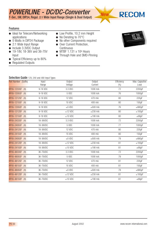
Input Filter Output Voltage Accuracy Output Voltage Balance Ripple and Noise, 20MHz BW Line Regulation Load Regulation, FL-1/4FL Efficiency Temperature Coefficient Over Current Protection Switching Frequency Isolation Voltage, Standard Models
元器件交易网
POWERLINE - DC/DC-Converter
PM5S-S中文资料
PM5S-M-24-240V
SCALE DEI TEMPI
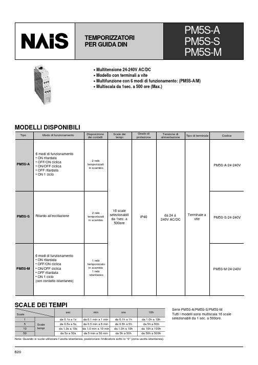
Scale 1 5 10 50 Scale tempi sec da 0.1s a 1s da 0.5s a 5s da 1.0s a 10s da 5s a 50s min da 0.1 min a 1 min da 0.5 min a 5 min da 1.0 min a 10 min da 5 min a 50 min ore da 0.1h a 1h da 0.5h a 5h da 1.0h a 10h da 5h a 50h 10h da 1.0h a 10h da 5h a 50h da 10h a 100h da 50h a 500h
da 1s a 500 ore 16 scale selezionabili ±0.3% ± 10% (del valore di fondo scala) ±1% (con variazione della tensione max da 85 a 110%) ±2% (con temperatura ambiente 20°C in un range da –10 a +50°C) 1 in scambio 2 contatti in scambio e 1 istantaneo Max. 100mΩ (da 1A 6V DC) Lega in argento Lega di argento placcata oro 2×10⁷ 105 da 85% a 110% sulla tensione nominale Tra ingresso ed uscita Min. 100MΩ Tra la parte attiva e l’involucro Tra i contatti 2,000Vrms per 1 minuti tra ingresso ed uscita 2,000Vrms per 1 minuto tra la parte attiva e l’involucro 1,000Vrms per 1 minuto tra i contatti 100ms 55°C Min. 98m/s2 (4 volte nelle 3 direzioni) Min. 980m/s2 (5 volte nelle 3 direzioni) da 10 a 55Hz: (1 ciclo min.) - con doppia ampiezza di 0.5 (10 min. nelle 3 direzioni) da 10 a 55Hz: con doppia ampiezza di 0.75 mm (1 ora nelle 3 direzioni) da –10 a +55°C Max. 85%RH da 860 a 1,060hPa 20% IP40 120g 130g
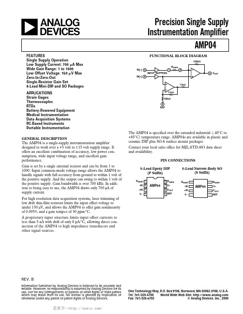
AMP04FSZ,AMP04FPZ,AMP04EPZ,AMP04FSZ-RL,AMP04FSZ-R7,AMP04FS-REEL7,AMP04ESZ-R7, 规格书,Datasheet 资料
One Technology Way, P.O. Box 9106, Norwood, MA 02062-9106, U.S.A.
Tel: 781/329-4700 World Wide Web Site:
Fax: 781/326-8703
© Analog Devices, Inc., 2000
For high resolution data acquisition systems, laser trimming of low drift thin-film resistors limits the input offset voltage to under 150 µV, and allows the AMP04 to offer gain nonlinearity of 0.005% and a gain tempco of 30 ppm/°C.
1000 1 0.005 0.015 0.025 30
0.75 %
1.0 %
0.75
%
1000 V/V
%
%
%
50
ppm/°C
OUTPUT Output Voltage Swing High
Output Voltage Swing Low Output Current Limit
VOH
RL = 2 kΩ
Contact your local sales office for MIL-STD-883 data sheet and availability.
PIN CONNECTIONS
8-Lead Epoxy DIP (P Suffix)
8-Lead Narrow-Body SO (S Suffix)
25
RSO-0505S;RSO-0505D;RSO-2412DZ;RSO-2405SZH3;RSO-243.3S;中文规格书,Datasheet资料

ECONOLINEDC/DC-Converterwith 3 year WarrantyRSO E-95REV:1/2011EN-60950-1 Certified EN-60601-1 CertifiedDescriptionHigh-power-density, an industrial temperature range of -40°C to +85°C and extra features like On-Off-control are just some of the characteristics of this converter, ideal for highly sophisticated industrial-designs. The RSO series is available with isolation of 2kV or 3kV by chosing option "/H2"or "/H3" in which case it is also ideal for medical applications which additionally require EN-60601-1 certification. The standard version offers 2:1 input voltage range, while the “Z” version features 4:1input voltage range, which includes an input voltage range covering both 5V and 12V supplies.1 WattSIP8 Isolated Single &Dual Output●2:1 and 4:1 Wide Input Voltage Ranges ●1kVDC, 2kVD or 3kVDC Isolation ●UL94V-0 Package Material●Certified for Medical Applications ●Continuous Short Circuit Protection ●Low Noise●No External Capacitor needed ●Efficiency to 83%FeaturesRegulated ConvertersSelection GuidePart NumberInput Rated Output Output Current Efficiency Max Voltage Range Voltage typ.CapacitiveSIP8(VDC)(VDC)(mA)(%)Load (1)RSO-xx3.3S* 4.5-9**, 9-18 3.330068-723300µF18-36, 36-7270RSO-xx05S* 4.5-9**, 9-18520073-751200µF18-36, 36-7275-78RSO-xx09S* 4.5-9**, 9-18911174-78680µF18-36, 36-7278-81RSO-xx12S* 4.5-9**, 9-18128375-80680µF18-36, 36-7280-83RSO-xx15S* 4.5-9**, 9-18156775-80680µF18-36, 36-7280-83RSO-xx3.3D* 4.5-9**, 9-18±3.3±15068-72±1500µF18-36, 36-7270RSO-xx05D* 4.5-9**, 9-18±5±10073-75±470µF18-36, 36-7275-76RSO-xx09D* 4.5-9**, 9-18±9±5674-78±470µF18-36, 36-7278RSO-xx12D* 4.5-9**, 9-18±12±4275-79±330µF18-36, 36-7279-80RSO-xx15D* 4.5-9**, 9-18±15±3475-79±330µF18-36, 36-7279-80RSO-xx3.3SZ*9-36 3.330068-703300µF18-7270RSO-xx05SZ* 4.5-18**, 9-36520073-781200µF18-7275RSO-xx09SZ* 4.5-18**, 9-36911175-81680µF18-7278RSO-xx12SZ* 4.5-18**, 9-36128377-83680µF18-7280RSO-xx15SZ* 4.5-18**, 9-36156778-83680µF18-7280RSO-xx3.3DZ*9-36±3.3±15070-74±1500µF18-7270RSO-xx05DZ* 4.5-18**, 9-36±5±10073-77±470µF18-7275RSO-xx09DZ* 4.5-18**, 9-36±9±5674-78±470µF18-7278RSO-xx12DZ* 4.5-18**, 9-36±12±4275-80±330µF18-7280RSO-xx15DZ* 4.5-18**, 9-36±15±3475-80±330µF18-7280No suffix is standard isolation (1kVDC) e.g, RSO-0505S*add suffix /H2 or /H3 for 2kVDC or 3kVDC isolation, e.g, RSO-0505S/H2, RSO-0505DZ/H3** derate to 75% if Vin<5V, 12V 4:1 input also requires an external 10µF input capacitor.Refer to Application NotesRoHS2002/95/EC6/6O u t p u t P o w e r (%)100602040Operating Temperature °C80Derating-Graph(Ambient T emperature)2:1Input 4:1Input (RS0-S/D) (RSO-SZ/DZ)xx = 4.5-9Vin = 05 xx = 4.5-18Vin = 12xx = 9-18Vin = 12 xx = 9-36Vin = 24 xx = 18-36Vin = 24 xx = 18-72Vin = 48xx = 36-72Vin = 48/E-96REV: 1/2011R S 0Input Voltage Range 2:1 and 4:1Output Voltage Accuracy ±2% typ.Line Voltage Regulation 2:1±0.2% max.4:1±0.5% max.Load Voltage Regulation 2:1±0.4% max.(10% to 100% full load)4:1±0.5% typ.Minimum Load0%Output Ripple and Noise (20MHz limited)50mVp-p max.Operating Frequency 2:1200kHz min. / 500kHz max.4:1100kHz min. / 800kHz max.Efficiency at Full Load See Selection GuideQuiescent Current RSO-05xxS_D, SZ_DZ 40mA typ.Nominal input Voltage RSO-12xxS_D32mA typ.(Standard, /H2 and /H3)RSO-24xxS_D, SZ_DZ 25mA typ.RSO-48xxS_D, SZ_DZ15mA typ.CTRL Pin drive current /see Notes)3mA typ, 6mA max.Quiescent Input Current when Converter is OFF 10mA max.Isolation Voltage Standard (tested for 1 second)1000VDC(rated for 1 minute)500VAC / 60Hz/H2 Version (tested for 1 second)2000VDC(rated for 1 minute)1000VAC / 60Hz/H3 Version (tested for 1 second)3000VDC(rated for 1 minute)1500VAC / 60HzIsolation Capacitance Standard 2:1 Single 10pF min. / 40pF typ. / 60pF max.Isolation Capacitance /H2 and /H32:1 Single 5pF min. / 30pF typ. / 60pF max.Isolation Capacitance Standard 2:1 Dual 120pF min. / 170pF typ. / 250pF max.Isolation Capacitance /H2 and /H32:1 Dual 5pF min. / 30pF typ. / 60pF max.Isolation Capacitance Standard 4:1 Single/Dual 200pF max.Isolation Capacitance /H2 and /H34:1 Single/Dual 30pF max.Isolation Resistance >1G Ωmin.Short Circuit ProtectionContinuousOperating Temperature Range (free air convection)-40°C to +85°C (see Graph)Storage Temperature Range -55°C to +125°CRelative Humidity 95% RH Package Weight 4.7gPacking Quantity 22 pcs per TubeMTBF (+25°C)using MIL-HDBK 217F 1685 x 103 hours (+85°C)using MIL-HDBK 217F254 x 103 hoursSpecifications (Core Operating Area)measured at T A = 25°C, nominal input voltage, full load and after warm-up time unless otherwise specifiedTypical ApplicationE f f i c i e n c y %100040%0%100%40Efficiency / Load 60%80%20%206080Total Output current (%)RSO-24xxS}Detailed Information seeApplication Notes chapter "MTBF"-Vin-Vout+Vout+VinE f f i c i e n c y %100040%0%100%40Efficiency / Load 60%80%20%206080Total Output current (%)RSO-1205SZ/RSO E-97REV:1/20113rd angleprojection8 PIN SIP PackageXX.X ± 0.5 mm XX.XX ± 0.25 mmPin 8 (NC*)This pin is used internally and must have no external connection.Pin 5 (NC)Not connected internally.Pin 3 (CTRL)This pin provides an Off function which puts the converter into a low power mode. When the pin is ‘high’ the converter is OFF and when the pin is high ‘Z’ the converter is ON. There is no allowed low state for this pin.Package Style and Pinning (mm)Single Output Recommended Footprint DetailsPin Connections Pin #SingleDual1 –Vin –Vin2 +Vin +Vin 3CTRL CTRL 5NC NC 6+Vout +Vout7 –Vout C om8NC*–VoutNC = No ConnectionNC* = NC, but no external Connection allowed.CTRL Examples+VoutCtrlTTL Remote CTRL CircuitVoltage to be applied via a limiting resistor with a recom-mended value of 1K for RSO-05xx; 3.3K for RSO-12xx;4.7K for RSO-24xx and 10K for RSO-48xx.Control Pin Input Current: 10mA Voltage Set Point Accuracy with external input/outputcapacitors refer to typ. ± 1%recommended test circuit: max. ±2%Control Pin (CTRL) Input Current, control voltage applied via 1K resistor,output voltage must typ. 3mA reduce to 0V: max. 6mA+VoutIsolated Remote CTRL CircuitNotes Note 1Maximum capacitive load is defined as the capacitive load that will allow start up in under 1 second without damage to the converterCertifications EN General Safety Report: IL-R7109EN60950-1:2001 + A11:2004EN Medical SafetyReport: PS071001601EN60601-1:1990 + A11:1996/分销商库存信息:RECOM-POWERRSO-0505S RSO-0505D RSO-2412DZ RSO-2405SZ/H3RSO-243.3S RSO-1212S RSO-2412D RSO-2415D RSO-0505S/H2 RSO-2405SZ/H2RSO-2405DZ RSO-0505S/H3 RSO-2412SZ/H3RSO-1205DZ RSO-1212DZ RSO-2415DZ/H3RSO-2412DZ/H3RSO-4812SZ/H3 RSO-4805SZ/H3RSO-4812DZ/H3RSO-4815DZ/H3 RSO-2409S RSO-1209S RSO-1215S RSO-123.3S RSO-2415S RSO-2412S RSO-2405S RSO-0509S RSO-0512S RSO-053.3S RSO-2409SZ RSO-2412SZ RSO-2415SZ RSO-243.3SZ RSO-4805S RSO-4809S RSO-4812S RSO-4815S RSO-483.3S RSO-1205S RSO-0509D RSO-0509S/H2RSO-0512D RSO-0512S/H2 RSO-0515D RSO-0515S/H2RSO-053.3D RSO-053.3S/H2RSO-2409DZ RSO-2409SZ/H2 RSO-2412SZ/H2RSO-2415DZ RSO-2415SZ/H2 RSO-243.3DZ RSO-243.3SZ/H2RSO-1205S/H3 RSO-1209S/H3RSO-1212S/H3RSO-1215S/H3 RSO-123.3S/H3RSO-2405S/H2RSO-2409S/H2 RSO-2412S/H2RSO-2415S/H2RSO-243.3S/H2 RSO-2405D RSO-2409D RSO-243.3D RSO-2405D/H2RSO-2409D/H2RSO-2412D/H2 RSO-2415D/H2RSO-243.3D/H2RSO-1205S/H2 RSO-1209S/H2RSO-1212S/H2RSO-1215S/H2 RSO-123.3S/H2RSO-1205D RSO-1209D RSO-1212D RSO-1215D RSO-123.3D RSO-0515S RSO-2405SZ RSO-1209SZ RSO-1215SZ RSO-123.3SZ RSO-0509S/H3 RSO-0512S/H3RSO-0515S/H3RSO-053.3S/H3 RSO-1205D/H2RSO-1209D/H2RSO-1212D/H2 RSO-1215D/H2RSO-123.3D/H2RSO-2409SZ/H3 RSO-2415SZ/H3RSO-243.3SZ/H3RSO-1205SZ/H2 RSO-1209DZ RSO-1209SZ/H2RSO-1212SZ/H2 RSO-1215DZ RSO-1215SZ/H2RSO-123.3DZ RSO-123.3SZ/H2RSO-4805SZ RSO-4809SZ RSO-4812SZ RSO-4815SZ RSO-483.3SZ RSO-2409S/H3RSO-2412S/H3RSO-2415S/H3 RSO-243.3S/H3RSO-2405D/H3RSO-2409D/H3 RSO-2412D/H3RSO-2415D/H3RSO-243.3D/H3 RSO-4805D RSO-4805S/H2RSO-4809D RSO-4809S/H2RSO-4812D RSO-4812S/H2 RSO-4815D RSO-4815S/H2RSO-483.3D。
RK-0505S中文资料

0% 20% 40% 60% Total Output current (%)
80%
100%
0% 20% 40% 60% Total Output current (%)
80%
100%
April-2005
39
元器件交易网
80%
100%
0% 20% 40% 60% Total Output current (%)
80%
100%
0%
20%
40%
60%
80%
100%
Total Output current (%)
Deviation / Load
25.000 20.000 25.000 20.000
Deviation / Load
Safe Operating Area
85 Operating Temperature °C
-40
0
50
100
150
38
April-2005
元器件交易网
ECONOLINE
DC/DC-Converter
Specifications (Core Operating Area)
Output Power (%)
100 80 60 40 30 20 0
Derating-Graph
(Ambient Temperature)
(tested for 1 second) (long term isolation) (tested for 1 second) (long term isolation) RK types RH types
4.000VDC min. see Application Notes. 20pF min. / 75pF max. 20pF min. / 65pF max. 15 GΩ min. 1 Second -40°C to +85°C (see Graph) -55°C to +125°C 95% RH continued on next page
LT2005-S中文资料
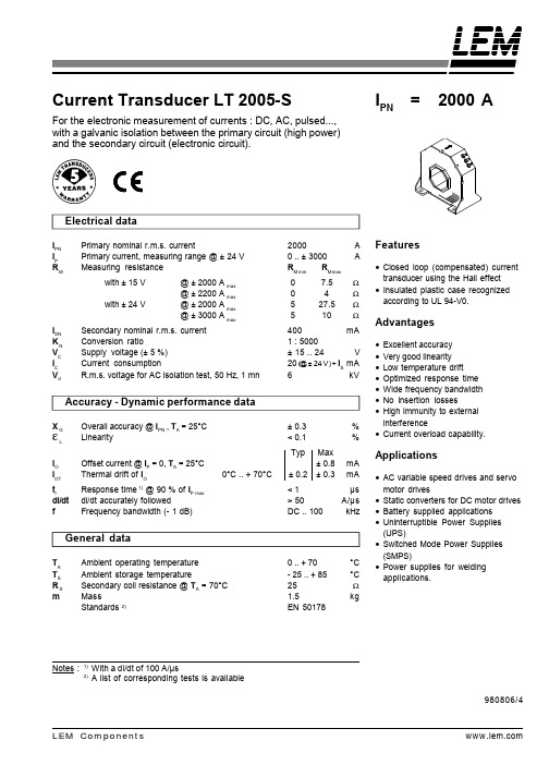
For the electronic measurement of currents : DC, AC, pulsed..., with a galvanic isolation between the primary circuit (high power) and the secondary circuit (electronic circuit).
6
kV
± 0.3
%
< 0.1
%
Typ Max ± 0.8 mA
± 0.2 ± 0.3 mA
<1 > 50 DC .. 100
µs A/µs
kHz
0 .. + 70
°C
- 25 .. + 85
°C
25
Ω
1.5Βιβλιοθήκη kgEN 50178
Features
•Closed loop (compensated) current transducer using the Hall effect
•IS is positive when IP flows in the direction of the arrow. •Temperature of the primary conductor should not exceed
100°C. •Dynamic performances (di/dt and response time) are best
with a single bar completely filling the primary hole. •This is a standard model. For different versions (supply
R09L05中文资料
4.1 min. 5.08
0.50±0.05
GND VIN 0V +V
1.25 typ.
0.25±0.05
7.62
0.25±0.05 1.9 7.62
1.25 typ.
1.9
7.62
Recommended Footprint Details
2.54 2.54
1.00ø+0.15/–0 2.54 2.54
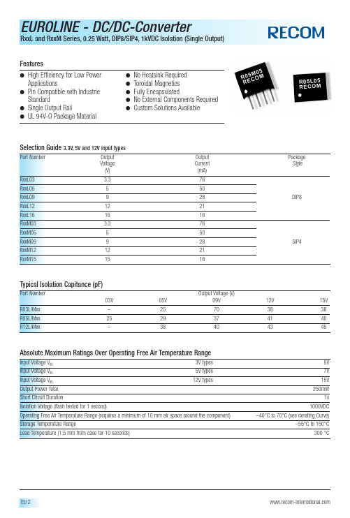
Absolute Maximum Ratings Over Operating Free Air Temperature Range
Input Voltage VIN Input Voltage VIN Input Voltage VIN Output Power Total Short Circuit Duration Isolation Voltage (flash tested for 1 second) Operating Free Air Temperature Range (requires a minimum of 10 mm air space around the component) Storage Temperature Range Lead Temperature (1.5 mm from case for 10 seconds) 3V types 5V types 12V types 5V 7V 15V 250mW 1s 1000VDC –40°C to 70°C (see derating Curve) –55°C to 150°C 300 °C
Temper. Derating Graph
0.500 Output Power (Watts)
+5%
R05H15资料
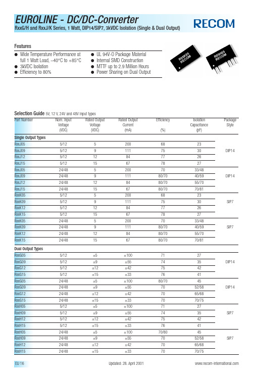
Dual Output TypesRxxG055/12±5±1007127RxxG095/12±9±557435DIP14 RxxG125/12±12±427542RxxG155/12±15±337641RxxG0524/48±5±10080/7045RxxG0924/48±9±557052/58DIP14 RxxG1224/48±12±427065/68RxxG1524/48±15±337070/75RxxH055/12±5±1007127RxxH095/12±9±557435SIP7 RxxH125/12±12±427542RxxH155/12±15±337641RxxH0524/48±5±10070/8045RxxH0924/48±9±557052/58SIP7 RxxH1224/48±12±427065/68RxxH1524/48±15±337070/75Absolute Maximum RatingsInput Voltage V IN5V types 7V typ.12V types 15V typ.24V types 24V typ.48V types48V typ.Short Circuit Duration 1)1s Internal Power Dissipation560mW Lead Temperature (1.5 mm from case for 10 seconds)300 °C1).Supply voltage must be discontinued at the end of the short circuit duration.Input Voltage Range V IN (continuous operation)5V input types 4.5VDC min./ 5.5VDC max.12V input types 10.8VDC min./ 13.2VDC max.24V input types 28VDC max.48V input types54VDC max.Reflected Ripple Current (depending on the type)20 mA p-p min.to 40 mA p-p max.Voltage Set Point Accuracy See Tolerance EnvelopeLine Regulation1.0% / 1.2% of V INLoad Voltage Regulation (10% load to 100% full load)single output types 6.7% min./ 15% max.dual output types 6.8% min./ 10% max.Ripple & Noise (20MHz band limited)single output types 32mVp-p min./ 80mVp-p max.dual output types24mVp-p min./ 40mVp-p max.Isolation Voltage (for 1 minute)3000VDC min.Test Voltage (50Hz,10 seconds)3000 Vpk min.Resistance (Viso = 1000V)10 G Ωtyp.Switching Frequency at Full Load (depending on the type)V IN 5V output types 120kHz min./ 135kHz max.V IN 12V output types 150kHz min./ 170kHz max.V IN 24V output types 150kHz max.V IN 48V output types150kHz max.Package Weight2.11 gOperating Temperature Range (all output types)–40°C min.to +85°C max.(see graph)Storage Temperature Range–50°C min.+125°C max.Case Temperature Above Ambient (depending on the type)5V output types+28°C max.all other output types +25°C max.MTTF 1) (depending on the type)–40°C,single output types 303kHrs min./ 2938kHrs max.+25°C,single output types 252kHrs min./ 2414kHrs max.+85°C,single output types 212kHrs min./ 1961kHrs max.–40°C,dual output types 185kHrs min./ 2068kHrs max.+25°C,dual output types 154kHrs min./ 1697kHrs max.+85°C,dual output types130kHrs min./ 1368kHrs max.1).Calculated using MIL-HDBK-217F with nominal input voltage at full load.Please contact us,if you need exact parameters for the converter you have selected.Electrical Specifications (measured at T A = 25°C,at nominal input voltage and rated output current unless otherwise specified)Package Style and Pinning (mm)。
05s2l-05s6l.pdf 表面贴装肖特基势垒二极管数据表说明书

VOLTAGE RANGE 20 to 60 Volts CURRENT 0.5 AmpereMAXIMUM RATINGS (@ T A =25 C unless otherwise noted)ELECTRICAL CHARACTERISTICS (@T A =25 C unless otherwise noted)RATINGSMaximum Recurrent Peak Reverse Voltage Maximum RMS Voltage Maximum DC Blocking VoltageMaximum Average Forward Rectified Current .375” (9.5mm) lead length at T A =550CPeak Forward Surge Current 8.3 ms single half sine-wave superimposed on rated load (JEDEC method)Typical Junction Capacitance (Note 1)SYMBOL V RRM V R q JA R q JL DC I FSM C J T STGV RMS UNITS Volts Volts Volts Amps 0.51511030110Amps 0C 0C/W 0C/WStorage Temperature RangeI O 150pFOperating T Typical Thermal Resistance (Note 3)emperature Range T J 05S2L 05S4L 05S5L 05S6L 05S3L 204050603014283542212040506030-55 to + 150CNOTES : 1. Measured at 1 MHz and applied reverse voltage of 4.0 volts.2006-11CHARACTERISTICSMaximum Average Reverse Current at Rated DC Blocking VoltageV F SYMBOL I RmAmps Maximum Instantaneous Forward Voltage at 0.5A DC Volts 0.22@T A = 25oC @T A = 100o C.55.70mAmps UNITS 05S2L 05S4L 05S5L05S6L 05S3L 2. 3. Thermal Resistance: Mounted on PCB.“Fully ROHS compliant”, “100% Sn plating (Pb-free)”.INSTANTANEOUS FORWARD VOLTAGE, (V)PERCENT RATED PEAK REVERSE VOLTAGE, (%)I N S T A N T A N E O U S F O R W A R D C U R R E N T , (A )AMBIENT TEMPERATURE, (C)0.10.11.01020A V E R A G E F O R W A R D C U R R E N T , (A )C T , T O T A L C A P A C I T A N C E , (p F )0.10.20.30.40.51.7 1.91.30.50.30.90.7 1.1 1.52.117515012510075502500.0010.10.011.010100RATING AND CHARACTERISTICS CURVES ( 05S2L THRU 05S6L )FIG.3 TYPICAL REVERSE CHARACTERISTICSFIG.1 TYPICAL FORWARD CURRENT DERATING CURVEFIG.2 TYPICAL INSTANTANEOUSREVERSE VOLTAGE, (V)I NS T A N T A NE O U S R E V E R S E C U R R E N T , (m A )1010080604020200400FIG.4 TYPICAL JUNCTION CAPACITANCE PERCENT RATED PEAK REVERSE VOLTAGE, (%)0.0010.10.011.010100FIG.3 TYPICAL REVERSE CHARACTERISTICSI N S T A N T A N E O U S R E V E R S E C U R R E N T , (m A )NUMBER OF CYCLES AT 60HzP E A K F O R W A R D S U R G E C U R R E N T , (A )105152520FIG.5 MAXIMUM NON-REPETITIVE FORWARD SURGE CURRENTMounting Pad LayoutDimensions in inches and (millimeters).052 MIN.(1.32 MIN.).033 MIN..033 MIN.(0.85 MIN.)Rectron Inc reserves the right to make changes without notice to any productspecification herein, to make corrections, modifications, enhancements or other changes. Rectron Inc or anyone on its behalf assumes no responsibility or liabi- lity for any errors or inaccuracies. Data sheet specifications and its information contained are intended to provide a product description only. "Typical" paramet- ers which may be included on RECTRON data sheets and/ or specifications ca- n and do vary in different applications and actual performance may vary over ti- me. Rectron Inc does not assume any liability arising out of the application or use of any product or circuit.Rectron products are not designed, intended or authorized for use in medical, life-saving implant or other applications intended for life-sustaining or other rela- ted applications where a failure or malfunction of component or circuitry may di- rectly or indirectly cause injury or threaten a life without expressed written appr- oval of Rectron Inc. Customers using or selling Rectron components for use in such applications do so at their own risk and shall agree to fully indemnify Rect- ron Inc and its subsidiaries harmless against all claims, damages and expendit- ures.DISCLAIMER NOTICE。
PSR05中文资料
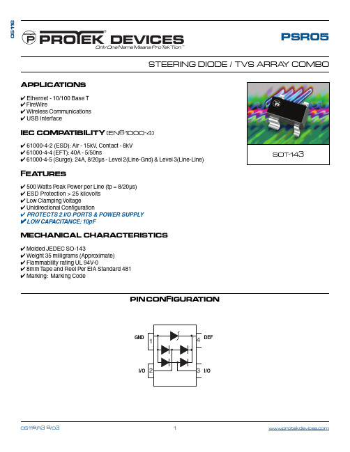
PSR05STEERING DIODE / TVS ARRA Y COMBOOnly One Name Means ProTek’Tion™APPLICA TIONS ✔ Ethernet - 10/100 Base T✔ FireWire✔ Wireless Communications ✔ USB InterfaceIEC COMP A TIBILITY (EN61000-4)✔ 61000-4-2 (ESD): Air - 15kV , Contact - 8kV ✔ 61000-4-4 (EFT): 40A - 5/50ns✔ 61000-4-5 (Surge): 24A, 8/20µs - Level 2(Line-Gnd) & Level 3(Line-Line)FEA TURES✔ 500 Watts Peak Power per Line (tp = 8/20µs)✔ ESD Protection > 25 kilovolts ✔ Low Clamping Voltage✔ Unidirectional Configuration✔ PROTECTS 2 I/O PORTS & POWER SUPPLY ✔ LOW CAPACITANCE: 10pFMECHANICAL CHARACTERISTICS ✔ Molded JEDEC SO-143✔ Weight 35 milligrams (Approximate)✔ Flammability rating UL 94V-0✔ 8mm Tape and Reel Per EIA Standard 481✔ Marking: Marking Code05116PIN CONFIGURA TIONSOT -143GNDI/OREFI/ODEVICE CHARACTERISTICSNote 1: As shown in Figure 5, REF 1 is connected to ground, REF 2 is connected to +V CC and input applies to V CC = 5V , V sign = 30mV , F = 1MHz.ELECTRICAL CHARACTERISTICS PER LINE @ 25°C Unless Otherwise SpecifiedPART NUMBERMINIMUM BREAKDOWN VOLTAGE@ 1A V (BR)VOLTS MAXIMUM CLAMPING VOLTAGE (See Fig. 2)@ I P = 1AV C VOLTS MAXIMUM CLAMPING VOLTAGE (See Fig. 2)8/20µs V C @ I PP VOLTS MAXIMUM CAPACITANCE (See Note 1)(See Fig. 5)(Per Data Line)@0V , 1 MHzC J(SD)pFPSR056.09.820.0V @ 28.0A10MAXIMUM LEAKAGE CURRENT@V WMI D µA 5.0RATED ST AND-OFF VOLTAGEV WM VOLTS5.0DEVICE MARKING5AMAXIMUN RATINGS @ 25°C Unless Otherwise SpecifiedOperating T emperature SYMBOL VALUE -55°C to 150°C°C °C -55°C to 150°C UNITS T J T STG PARAMETERStorage T emperaturePeak Pulse Power (t p = 8/20µs) - See Figure 1P PP 500Watts Peak Forward Voltage - I F = 1A, 8/20µsVolts1.5VF0 5 10 15 20 25 30t - Time - µs20406080100120I P P - P e a k P u l s e C u r r e n t - % o f I P PFIGUR E 20.01 1 10 100 1,000 10,000t d - Pulse Duration - µs101001,00010,000P P P - P e a k P u l s e C u r r e n t - W a t t sFIGUR E 1PEAK PULSE POWER VS PULSE TIMEGRAPHSFIGUR E 5INPUT CAPACITANCE CIRCUITCCV SIGNT L - Lead T emperature - °C20406080100% O f R a t e d P o w e rFIGUR E 3FIGUR E 4OVER SHOOT & CLAMPING VOLTAGE FOR PSR 05ESD Test Pulse: 5 kilovolt, 1/30ns (waveform)5 V o l t s p e r D i v i s i o n-20-101020FIGUR E 6TYPICAL REVERSE VOLTAGE VS CAPACITANCE FOR PSR050 1 2 3 4 5V R - Reverse Voltage - VoltsC - C a p a c i t a n c e - p F481216APPLICA TION NOTEThe PSR05 is a low capacitance, bidirectional TVS array that is designed to protect I/O or high speed data lines from the damaging effects of ESD or EFT. This product series has a surge capability of 500 Watts PPPper line for an 8/20µs waveform and offers ESD protection > 25kV.COMMON-MODE CONFIGUR ATION (Figure 1)Ideal for use in USB applications, two PSR05 devices provides up to two(2) lines of protection(per device) in a common-mode configuration as depicted in Figure 1.Circuit connectivity is as follows:✔Pins 2 and 3 are connected to the datalines.✔Pin 1 is connected to ground.✔Pin 4 is connected to the databus.CIR CUIT BOAR D LAYOUT R ECOMMENDATIONS Circuit board layout is critical for Electromagnetic Compatibility (EMC) protection. The following guidelines are recommended:✔The protection device should be placed near the input terminals or connectors, the device willdivert the transient current immediately before itcan be coupled into the nearby traces.✔The path length between the TVS device and the protected line should be minimized.✔All conductive loops including power and ground loops should be minimized.✔The transient current return path to ground should be kept as short as possible to reduceparasitic inductance.✔Ground planes should be used whenever possible. For multilayer PCBs, use ground vias.Figure 1. T ypical Common-Mode USB ProtectionCOPYR IGHT © ProTek Devices 2003SPECIFICA TIONS: ProT ek reserves the right to change the electrical and or mechanical characteristics described herein without notice (except JEDEC).DESIGN CHANGES: ProT ek reserves the right to discontinue product lines without notice, and that the final judgement concerning selection and specifications is the buyer ’s and that in furnishing engineering and technical assistance, ProTek assumes no responsibility with respect to the selection or specifications of such products.P ACKAGE OUTLINE & DIMENSIONSProTek Devices2929 South Fair Lane, Tempe, AZ 85282Tel: 602-431-8101 Fax: 602-431-2288E-Mail: sales@ Web Site: 。
PQ09RF12资料
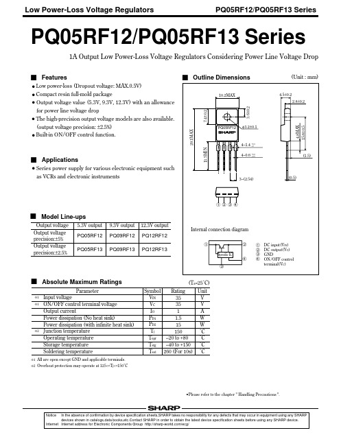
Low Power-Loss Voltage Regulators PQ05RF12/PQ05RF13 Seriess Featuresq Low power-loss (Dropout voltage: MAX.0.5V) q Compact resin full-mold packageq Output voltage value (5.3V, 9.3V, 12.3V) with an allowance for power line voltage dropq The high-precision output voltage models are also available.(output voltage precision: ±2.5%) q Built-in ON/OFF control function.s Applicationsq Series power supply for various electronic equipment such as VCRs and electronic instrumentsPQ05RF12/PQ05RF13 Seriess Outline Dimensions(Unit : mm)1A Output Low Power-Loss Voltage Regulators Considering Power Line Voltage DropParameterSymbol Rating Unit V IN V C I O P D1P D2T j T opr T stg T sol 353511.515150–20 to +80 –40 to +150260 (For 10s)V V A W W ˚C ˚C ˚C ˚CInput voltageON/OFF control terminal voltage Output currentPower dissipation (No heat sink)Power dissipation (with infinite heat sink)Junction temperature Operating temperature Storage temperature Soldering temperature❇1❇1❇2❇1 All are open except GND and applicable terminals.❇2 Overheat protection may operate at 125<=T j <=150˚Cs Absolute Maximum Ratings(T a =25˚C)Output voltagePQ05RF12PQ05RF13Output voltage precision:±5%Output voltage precision:±2.5%s Model Line-ups5.3V output PQ09RF12PQ09RF139.3V output PQ12RF12PQ12RF1312.3V output•Please refer to the chapter " Handling Precautions ".In the absence of confirmation by device specification sheets,SHARP takes no responsibility for any defects that may occur in equipment using any SHARP devices shown in catalogs,data books,etc.Contact SHARP in order to obtain the latest device specification sheets before using any SHARP device.Internet address for Electronic Components Group /ecg/Fig.1Test CircuitFig.2Test Circuit of Ripple Rejection0.5 1.0 1.5 2.0100804060200R e l a t i v e o u t p u t v o l t a g e (%)Output current I O (A)Parameter Symbol ConditionsV OR eg LR eg IT C V O RRV i -OV C (ON )I C (ON )V C (OFF )I C (OFF )I qOutput voltage Load regulation Line regulation Temperature coefficient of output voltage Ripple rejection Dropout voltage ON-state voltage for control ON-state current for control OFF-state voltage for control OFF-state current for control Quiescent current UnitMAX.TYP.MIN.PQ05RF12PQ09RF12PQ12RF12PQ05RF13PQ09RF13PQ12RF13PQ05RF12/13PQ09RF12/13PQ12RF12/135.048.8411.695.179.0712.0−−−45−2.0−−−−−I O =5mA to 1.0A V IN =7 to 17V, I O =5mA V IN =11 to 21V, I O =5mA V IN =14 to 24V, I O =5mA T j =0 to 125˚C, I O =5mA Refer to Fig. 2❇3❇4V C =2.7V −V C =0.4V V C =0A 5.39.312.35.39.312.30.10.5±0.0255−−−−−−5.569.7612.915.439.5312.62.02.5−−0.5−200.8–0.410V%%%/˚C dB V V µA V mA mAs Electrical Characteristics❇3 Input voltage shall be the value when output voltage is 95% in comparison with the initial value.❇4 In case of opening control terminal ➃, output voltage turns on.V IN = 8V, I O =0.5A (PQ05RF12/PQ05RF13)V IN =12V, I O =0.5A (PQ09RF12/PQ09RF13)V IN =15V, I O =0.5A (PQ12RF12/PQ12RF13)(T a =25˚C)Unless otherwise specified, condition shall be e i V of=120Hz(sine wave)RR=20 log(e i(rms)/e o(rms))I O =0.5A e i(rms)=0.5VV IN =8V(PQ05RF12/13)12V(PQ09RF12/13)15V(PQ12RF12/13)Low Power-Loss Voltage Regulators PQ05RF12/PQ05RF13 Series Fig.5Output Voltage Deviation vs. JunctionTemperature (PQ05RF12/PQ05RF13)Fig.7Output Voltage Deviation vs. Junction Temperature (PQ12RF12/PQ12RF13) Fig.9Output Voltage vs. Input Voltage(PQ09RF12/PQ09RF13)Fig.8Output Voltage vs. Input Voltage (PQ05RF12/PQ05RF13)Fig.10Output Voltage vs. Input VoltageFig.6Output Voltage Deviation vs. JunctionTemperature (PQ09RF12/PQ09RF13) 15010050–50–100Outputvoltagedeviation∆VO(mV)Junction temperature T j (˚C)20015010050–50–100–150Outputvoltagedeviation∆VO(mV)Junction temperature T j (˚C)–200–25050251007512525020015010050–50–100–150Outputvoltagedeviation∆VO(mV)Junction temperature T j (˚C)87654321OutputvoltageVO(V)Input voltage V IN (V) 051015OutputvoltageVO(V)Input voltage V IN (V)5101520OutputvoltageVO(V)Input voltage V IN (V)51010203040C i r c u i t o p e r a t i n g c u r r e n t I B I A S (m A )Input voltage V IN(V)1015510203040C i r c u i t o p e r a t i n g c u r r e n t I B I A S (m A )Input voltage V IN(V)0510152025C i r c u i t o p e r a t i n g c u r r e n t I B I A S (m A )Input voltage V IN (V)D r o p o u t v o l t a g e V i –O (V )Junction temperature T j (˚C)246810Q u i e s c e n t c u r r e n t I q (m A )Junction temperature T j (˚C)00.11011001020304050607080R i p p l e r e j e c t i o n R R (d B )Input ripple frequency f (kHz)Low Power-Loss Voltage RegulatorsPQ05RF12/PQ05RF13 SeriesFig.17Ripple Rejection vs. Output CurrentFig.19Output Peak Current vs. JunctionTemperatureFig.18Output Peak Current vs. DropoutVoltage1.0510151.5T j =25˚C 2.0O u t p u t p e a k c u r r e n t I O P (A )Dropout voltage V i –O (V)2.01.51.00.5O u t p u t p e a k c u r r e n t I O P (A )Junction temperature T j (˚C)304050607080R i p p l e r e j e c t i o n R R (d B )Output current I O (A)NOTICEq The circuit application examples in this publication are provided to explain representative applications of SHARP devices and are not intended to guarantee any circuit design or license any intellectual property rights. SHARP takes no responsibility for any problems related to any intellectual property right of a third party resulting from the use of SHARP's devices.q Contact SHARP in order to obtain the latest device specification sheets before using any SHARP device. SHARP reserves the right to make changes in the specifications, characteristics, data, materials, structure, and other contents described herein at any time without notice in order to improve design or reliability. Manufacturing locations are also subject to change without notice.q Observe the following points when using any devices in this publication. SHARP takes no responsibility for damage caused by improper use of the devices which does not meet the conditions and absolute maximum ratings to be used specified in the relevant specification sheet nor meet the following conditions:(i)The devices in this publication are designed for use in general electronic equipment designs such as:--- Personal computers--- Office automation equipment--- Telecommunication equipment [terminal]--- Test and measurement equipment--- Industrial control--- Audio visual equipment--- Consumer electronics(ii)Measures such as fail-safe function and redundant design should be taken to ensure reliability and safety when SHARP devices are used for or in connection with equipment that requires higher reliability such as:--- Transportation control and safety equipment (i.e., aircraft, trains, automobiles, etc.)--- Traffic signals--- Gas leakage sensor breakers--- Alarm equipment--- Various safety devices, etc.(iii)SHARP devices shall not be used for or in connection with equipment that requires an extremely high level of reliability and safety such as:--- Space applications--- Telecommunication equipment [trunk lines]--- Nuclear power control equipment--- Medical and other life support equipment (e.g., scuba).q Contact a SHARP representative in advance when intending to use SHARP devices for any "specific" applications other than those recommended by SHARP or when it is unclear which category mentioned above controls the intended use.q If the SHARP devices listed in this publication fall within the scope of strategic products described in the Foreign Exchange and Foreign Trade Control Law of Japan, it is necessary to obtain approval to export such SHARP devices. q This publication is the proprietary product of SHARP and is copyrighted, with all rights reserved. Under the copyright laws, no part of this publication may be reproduced or transmitted in any form or by any means, electronic or mechanical, for any purpose, in whole or in part, without the express written permission of SHARP. Express written permission is also required before any use of this publication may be made by a third party.q Contact and consult with a SHARP representative if there are any questions about the contents of this publication.。
- 1、下载文档前请自行甄别文档内容的完整性,平台不提供额外的编辑、内容补充、找答案等附加服务。
- 2、"仅部分预览"的文档,不可在线预览部分如存在完整性等问题,可反馈申请退款(可完整预览的文档不适用该条件!)。
- 3、如文档侵犯您的权益,请联系客服反馈,我们会尽快为您处理(人工客服工作时间:9:00-18:30)。
2974 x 103 hours 728 x 103 hours
元器件交易网
ECONOLINE
DC/DC-Converter
Typical Characteristics, Tolerance Envelope
RxxPxxS_D Series
Deviation from Nominal (%)
15.000 10.000 5.000 0.000 -5.000 -10.000
Deviation from Nominal (%)
R12P05D R05P05S
R05P09S
15.000 10.000 5.000 0.000 -5.000 -10.000
RxxP12/15S
Efficiency / Load
100 80 60
RxxP05/09S
Efficiency / Load
100 80 60 40
R05P05S
R05P09S
R12P12S
R24P15S
R12P05S Efficiency % R12P09S
40 20 0
Efficiency %
R24P15D
0% 20% 40% 60% Total Output current (%)
80%
100%
July-2006
45
元器件交易网
ECONOLINE
DC/DC-Converter
Package Style and Pinning (mm)
RxxP12/15D
Efficiency / Load
100 80 60
R05P05D
R05P09D
R12P12D
R24P12D
R12P09D Efficiency % R12P05D
40 20 0
Efficiency %
20 0
R24P15D
0%
20%
40%
60%
80%
100%
0%
20%
40%
60%
80%
100%
Total Output current (%)
Total Output current (%)
Deviation / Load
25.000 20.000 25.000 20.000
Deviation / Load
Deviation from Nominal (%)
15.000 10.000 5.000 0Байду номын сангаас000 -5.000 -10.000
EN-60950-1 Certified UL-60950-1 Certified EN-60601-1 Certified
Specifications
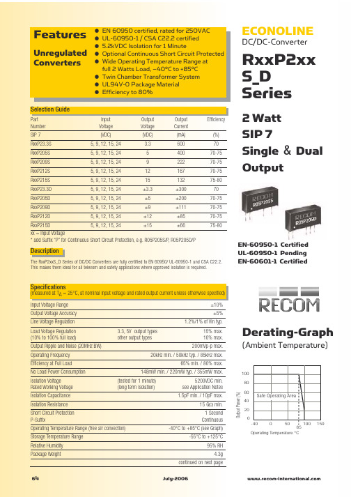
(measured at TA = 25°C, at nominal input voltage and rated output current unless otherwise specified) Input Voltage Range Output Voltage Accuracy Line Voltage Regulation Load Voltage Regulation (10% to 100% full load) Output Ripple and Noise (20MHz BW) Operating Frequency Efficiency at Full Load No Load Power Consumption Isolation Voltage Rated Working Voltage Isolation Capacitance Isolation Resistance Short Circuit Protection P-Suffix Operating Temperature Range (free air convection) Storage Temperature Range Relative Humidity Package Weight MTBF (+25°C) (+85°C) 44 (tested for 1 minute) (long term isolation) 3.3, 5V output types other output types ±10% ±5% 1.2%/1% of Vin typ. 15% max. 10% max. 200mVp-p max. 20kHz min. / 50kHz typ. / 85kHz max. 65% min. / 75% typ. 148mW min. / 220mW typ. / 355mW max. 5200VDC min. see Application Notes
ECONOLINE
DC/DC-Converter
RxxPxxS_D Series
1 Watt SIP 7 Single & Dual Output
Selection Guide
Part Number SIP 7 RxxP3.3S RxxP05S RxxP09S RxxP12S RxxP15S RxxP3.3D RxxP05D RxxP09D RxxP12D Input Voltage (VDC) 5, 9, 12, 15, 24 5, 9, 12, 15, 24 5, 9, 12, 15, 24 5, 9, 12, 15, 24 5, 9, 12, 15, 24 5, 9, 12, 15, 24 5, 9, 12, 15, 24 5, 9, 12, 15, 24 5, 9, 12, 15, 24 Output Voltage (VDC) 3.3 5 9 12 15 ±3.3 ±5 ±9 ±12 Output Current (mA) 303 200 111 84 66 ±151 ±100 ±55 ±41 Efficiency (%) 70 70-75 70-75 70-75 75-80 70 70-75 70-75 70-75 75-80
Deviation from Nominal (%)
R12P09D R05P05D
R05P09D
15.000 10.000 5.000 0.000 -5.000 -10.000
R12P12D
R24P12D
R12P05D
0% 20% 40% 60% Total Output current (%) 80% 100%
R12P12S
R24P12S
R24P15S
R12P05S
0% 20% 40% 60% Total Output current (%) 80% 100%
0% 20% 40% 60% Total Output current (%)
80%
100%
RxxP05/09D
Efficiency / Load
100 80 60 40
0.50
1 2
5 6 7
1 2
5
7
Recommended Footprint Details
19.50
Bottom View
Pin Connections Pin # 1 2 5 6 7 Single +Vin -Vin –Vout No Pin +Vout Dual +Vin –Vin –Vout Com +Vout
20 0
R24P12S
0%
20%
40%
60%
80%
100%
0%
20%
40%
60%
80%
100%
Total Output current (%)
Total Output current (%)
Deviation / Load
25.000 20.000 25.000 20.000
Deviation / Load
RxxP15D 5, 9, 12, 15, 24 ±15 ±33 xx = Input Voltage * add Suffix “P” for Continuous Short Circuit Protection, e.g. R05P05S/P, R05P05D/P
Description
The RxxPxxS_D Series of DC/DC Converters are fully certified to EN 60950/ UL-60950-1 and CSA C22.2. This makes them ideal for all telecom and safety applications where approved isolation is required.
元器件交易网
Features
Unregulated Converters
● ● ● ● ● ● ● ●
EN 60950 certified, rated for 250VAC UL-60950-1 / CSA C22.2 certified 5.2kVDC Isolation for 1 Minute Optional Continuous Short Circuit Protected Wide Temperature Performance at full 1 Watt Load, –40°C to +85°C 2 Chamber Transformer System UL94V-0 Package Material Efficiency to 80%
Output Power (%)
100 80 60 40 30 20 0
Derating-Graph
(Ambient Temperature)
4pF min. / 10pF max. 15 GΩ min. 1 Second Continuous -40°C to +85°C (see Graph) -55°C to +125°C 95% RH 4.3g
