AP8012C Datasheet中文版Rev B 1301
PMS150C datasheet V001_CN-1

PMS150C系列8位IO类型单片机数据手册第0.01版2016年3月17日Copyright 2016 by PADAUK Technology Co., Ltd., all rights reserved重要声明应广科技保留权利在任何时候变更或终止产品,建议客户在使用或下单前与应广科技或代理商联系以取得最新、最正确的产品信息。
应广科技不担保本产品适用于保障生命安全或紧急安全的应用,应广科技不为此类应用产品承担任何责任。
关键应用产品包括,但不仅限于,可能涉及的潜在风险的死亡,人身伤害,火灾或严重财产损失。
应广科技不承担任何责任来自于因客户的产品设计所造成的任何损失。
在应广科技所保障的规格范围内,客户应设计和验证他们的产品。
为了尽量减少风险,客户设计产品时,应保留适当的产品工作范围安全保障。
PMS150C不适用于交流供电阻容降压或者电源纹波大,EFT要求高的应用,请注意不要将PMS150C用于这种特殊要求的产品中。
提供本文档的中文简体版是为了便于了解,请勿忽视文中英文的部份,因为其中提供有关产品性能以及产品使用的有用信息,应广科技暨代理商对于文中可能存在的差错不承担任何责任,建议参考本档英文版。
目录1. 单片机特点 (7)1.1. 系统功能 (7)1.2. CPU特点 (7)2. 系统概述和方框图 (8)3. 引脚功能说明 (9)4. 器件电气特性 (10)4.1 直流交流电气特性 (10)4.2 工作范围 (11)4.3 IHRC频率与VDD关系曲线图 (12)4.4 ILRC频率与VDD关系曲线图 (12)4.5 IHRC频率与温度关系曲线图(校准到16MHz) (13)4.6 ILRC频率与温度关系曲线图 (13)4.7 工作电流与VDD、系统时钟CLK=IHRC/n曲线图 (14)4.8 工作电流与VDD、系统时钟CLK=ILRC/n曲线图 (14)4.9 引脚上拉电阻曲线图 (15)4.10 引脚输出驱电流(Ioh)与灌电流(Iol) 曲线图 (15)4.11 引脚输出输入高电压与低电压(V IH / V IL) 曲线图 (16)5. 功能概述 (17)5.1程序内存——OTP (17)5.2 开机流程 (17)5.3 数据存储器 – SRAM (18)5.4 振荡器和时钟 (18)5.4.1内部高频振荡器和内部低频振荡 (18)5.4.2芯片校准 (18)5.4.3 IHRC频率校准与系统时钟 (19)5.4.4系统时钟和LVR基准位 (20)5.5 16位定时器 (Timer16) (21)5.6 看门狗定时器 (22)5.7 中断 (22)5.8 省电与掉电 (24)5.8.1省电模式(stopexe) (24)5.8.2掉电模式(stopsys) (25)5.8.3 唤醒 (26)5.9 IO引脚 (27)5.10 复位和LVR (28)5.10.1复位 (28)6. IO 寄存器 (29)6.1 标志寄存器(flag),IO 地址 =0x00 (29)6.2 堆栈指针寄存器(sp),IO地址 =0x02 (29)6.3 时钟控制寄存器(clkmd),IO地址 =0x03 (29)6.4 中断允许寄存器(inten),IO地址 =0x04 (30)6.6 Timer16控制寄存器(t16m),IO地址 =0x06 (30)6.7 外部晶体振荡器控制寄存器(eoscr,只写),IO地址 =0x0a (31)6.8 中断缘选择寄存器 (integs), IO地址 =0x0c (31)6.9 端口A数字输入启用寄存器(padier), IO 地址 =0x0d (31)6.10 端口A数据寄存器(pa),IO地址 =0x10 (31)6.11 端口A控制寄存器(pac),IO地址 =0x11 (31)6.12 端口A上拉控制寄存器(paph),IO地址 =0x12 (31)6.13 杂项寄存器(misc), IO 地址 =0x3b (32)7. 指令 (33)7.1 数据传输类指令 (34)7.2 算术运算类指令 (36)7.3 移位元元运算类指令 (38)7.4 逻辑运算类指令 (39)7.5 位运算类指令 (41)7.6 条件运算类指令 (41)7.7 系统控制类指令 (42)7.8 指令执行周期综述 (44)7.9 指令影响标志的综述 (45)8. 特别注意事项 (46)8.1. 使用IC时 (46)8.1.1. IO使用与设定 (46)8.1.2. 中断 (46)8.1.3. 切换系统时钟 (47)8.1.4. 掉电模式、唤醒以及看门狗 (47)8.1.5. TIMER16溢出时间 (47) (47)8.1.6. LVR8.1.7. 指令 (47)8.1.8. RAM定义限制 (47)8.1.9. 烧录方法 (48)8.2. 使用ICE时 (48)修订历史:修订日期描述初版0.01 2016/3/17PMS150B 和PMS150C 主要差异表PMS150B 与PMS150C 主要差异列举如下:项目 功能PMS150BPMS150C1 ILRC 频率 110KHz@5.0V ,25oC 62KHz@5.0V ,25o C (VDD 变化对ILRC 有影响) 2 LVR 2.8V,2.2V,2.0V 4.0V,3.5V,3.0V,2.75V 2.5V,2.2V,2.0V,1.8V 3 RAM 60 bytes64 bytes 4 PA5口输入模式上拉电阻 没有有5 工作温度0o C ~70o C -20o C ~70o C6省电模式功耗(stopexe ) 40uA@3.3V3 uA@3.3V7 IO 输出电流 17mA/-7mA@5.0V普通模式:14.5mA/-10.5mA@5.0V低驱动模式:5mA/-3.5mA@5.0V 8 看门狗定时器溢时 4096,16384,65536 ILRC 时钟周期8192,16384,65536,262144 ILRC 时钟周期9 唤醒时间 快速模式:1024 T IHRC 普通模式:1024 T ILRC 快速模式:32 T ILRC 普通模式:2048 T ILRC 10 开机时间快速模式:2048 T IHRC 普通模式:1024 T ILRC快速模式:32 T ILRC 普通模式:2048 T ILRC 11系统保留OTP 区 0x3F8~0x3FF(8 word) 0x3F0~0x3FF(16 word)12 ILRC 做系统时钟源 ILRC,ILRC/4 ILRC,ILRC/4,ILRC/16 13支持ICE 类型PDK3S-I-001/002/003, 5S-I-S015S-I-S011. 单片机特点1.1. 系统功能◆时钟模式:内部高频振荡器、内部低频振荡器◆硬件16位定时器◆快速唤醒功能◆ 6 个带输入上拉电阻IO引脚,且做输出时具有可选的电流驱动能力◆1个外部中断输入引脚◆每个引脚都可弹性设定唤醒功能◆8级LVR可选◆工作频率0 ~ 8MHz@VDD≧3V; 0 ~ 4MHz@VDD≧2.2V; 0 ~ 2MHz@VDD≧2.0V;◆工作电压:2.0V ~ 5.5V◆工作温度:-20 o C ~70 o C◆功耗特性:I operating ~ 0.3mA@1MIPS, VDD=3.3VI operating ~ 13uA@ILRC=62KHz, VDD=3.3VI powerdown ~ 0.5uA@VDD=3.3V1.2. CPU特点◆工作模式:单一处理单元的工作模式◆ 1KW OTP程序内存◆ 64字节数据存储器◆提供79条指令◆绝大部分指令都是单周期(1T)指令◆可程序设定的堆栈深度◆所有的数据存储器都可当数据指针(index pointer)◆独立的IO地址以及存储地址方便程序开发2. 系统概述和方框图PMS150C是一个IO类型、完全静态,以OTP为程序存储基础的单片机。
ZLPM8012中文资料(Diodes)中文数据手册「EasyDatasheet - 矽搜」
专为稳定性与低功耗LNB 提供标准电压/语气和支持DiSEqC控制信号,并允许地区差 异. 为支持DiSEqC控制和传统内部22kHz发生器
波段开关
22kHz形状防护持在所有负载条件下 通过I C控制 内置多种诊断和防护护IC和LNB
防护护
最少外部元件简单,可靠和成本
有效解决方案
客户表示,他们有足够能力处理安全和他们生命支持设备可能产生后果或 系统,并承认和同意 ,他们全权负责所有法律 ,法规和安全相关要求 关于其产品任何使用Diodes公司产品等安全关键,生命支持设备或系统, 尽管可以通过 Diodes公司提供任何 devices-或系统有关信息或支持 .进一步, 客户必须全额赔偿Diodes公司及其代理人所产生使用二极管任何损失
生命防护障
Diodes公司产品特别是不授权没有生命支持设备或系统关键组件 快递Diodes公司首席执行官书面批准.如本文所用: A.生命支持设备或系统设备或系统,其中:
1.旨在植入到体内,或 2.支持或维持生命,其未履行时,正确使用符合规定使用说明
在标签可合理预期会导致显著伤害用户. B. 关键部件是在生命支持设备或系统 ,其不履行可以合理预期造成生命支持设备故障或影响其安全性或效力任何部 件.
完全无铅和符合 RoHS标准(注 1及 2) 卤素和无锑 . "绿色 "设备(注 3)
系统图
012
芯片中文手册,看全文,戳
ZLPM8012
芯片中文手册,看全文,戳
重要提醒
Diodes公司不做任何明示或暗示任何担防护,关于本 文件中,包括但不限于适销性和适用性暗示担防护适用于某 特殊目(及其任何司法管辖范围内法律等效). Diodes公司及其附属公司防护留权利作出修改,增强,改进,修正或其他变化,恕不另行通知本文档及其所涉及产品权利. Diodes公司不承担因使用或应用本文档或本文所述任何产品任何责任;既没有Diodes公司转达根据其专利权或商标权任何执照, 也没有他人权利.本文件或在这类应用产品本文所述任何客户或用户应承担所有使用风险,并同意举行Diodes公司,其产品代表 在Diodes公司网站,反对一切损害无害所有公司.
IKCS12F60F2A_C_Rev1_0_20100628(10)
F o r P o w e r M a n a g e m e n t A p p l i c a t i o nControl Integrated POwer System (CIPOS™)I K C S 12F 60F 2A I K C S 12F 60F 2CD a t a S he e t ,J un. 2010CIPOS™ IKCS12F60F2AIKCS12F60F2CRevision History: 2010-06Rev.1.0Authors: Junho Song*, Junbae Lee* and Daewoong Chung*, W. Frank**, W. Brunnbauer**LS Power Semitech*, Infineon Technologies**Edition 2010-01Published byLS Power Semitech Co., Ltd. Seoul, Korea© LS Power Semitech Co., Ltd.All Rights Reserved.Attention please!The information given in this data sheet shall in no event be regarded as a guarantee of conditions or characteristics. With respect to any examples or hints given herein, any typical values stated herein and/or any information regarding the application of the device, LS Power Semitech Co., Ltd. hereby disclaims any and all warranties and liabilities of any kind, including without limitation warranties of non-infringement of intellectual property rights of any third party.InformationFor further information on technology, delivery terms and conditions and prices please contact your nearest LS Power Semitech Co., Ltd. office or representatives ().WarningsDue to technical requirements components may contain dangerous substances. For information on the types in question please contact your nearest LS Power Semitech Co., Ltd. office or representatives.LS Power Semitech Co., Ltd. components may only be used in life-support devices or systems with the express written approval LS Power Semitech Co., Ltd., if a failure of such components can reasonably be expected to cause the failure of that life-support device or system, or to affect the safetyor effectiveness of that device or system. Life support devices or systems are intended to be implantedin the human body, or to support and/or maintain and sustain and/or protect human life. If they fail, it is reasonable to assume that the health of the user or other persons may be endangered.TRENCHSTOP® is a registered trademark of Infineon Technologies AG.CIPOS™ IKCS12F60F2AIKCS12F60F2CTable of contents:CIPOS™ Control Integrated POwer System (4)Features (4)Target Applications (4)Description (4)System Configuration (4)Certification (4)Internal Electrical Schematic (5)Pin Assignment (6)Pin Description (6)HIN1,2,3 and /LIN1,2,3 (Low side and high side control pins, Pin 15 - 20) (6)FLT-TEMP (temperature NTC, Pin 24) (7)ITRIP (Over-current detection function, Pin 21) (7)VDD, VSS (control side supply and reference, Pin 22, 23) (7)VB1,2,3 and VS1,2,3 (High side supplies, Pin 1, 2, 4, 5, 7, 8) (7)VRU, VRV, VRW (low side emitter, Pin 12, 13, 14) (7)V+ (positive bus input voltage, Pin 10) (7)Absolute Maximum Ratings (8)Module Section (8)IGBT and Diode Section (8)Control Section (9)Recommended Operation Conditions (9)Static Characteristics (10)Dynamic Characteristics (11)Integrated Components (12)Typical Application (12)Characteristics (13)Package Outline IKCS12F60F2A (17)Package Outline IKCS12F60F2C (18)CIPOS™ IKCS12F60F2AIKCS12F60F2CCIPOS™C ontrol I ntegrated PO wer S ystem Single In-Line Intelligent Power Module3Φ-bridge 600V / 12A @ 25°CFeatures•DCB isolated Single In-Line molded module •FAULT signal•TrenchStop® IGBTs with lowest V CE(sat)•Optimal adapted antiparallel diode for low EMI •Integrated bootstrap diode and capacitor •Rugged SOI gate driver technology with stability against transient and negative voltage •Fully compliant to 3.3V and 5V microcontrollers •Temperature sense•Under voltage lockout at all channels •Matched propagation delay for all channels •Low side emitter pins accessible for all phase current monitoring (open emitter)•Cross-conduction prevention•Lead-free terminal plating; RoHS compliant •Qualified according to JEDEC1 (high temperature stress tests for 1000h) for target applicationsTarget Applications•Washing machines•Consumer Fans and Consumer Compressors DescriptionThe CIPOS™ module family offers the chance for integrating various power and control components to increase reliability, optimize PCB size and system costs.This SIL-IPM is designed to control AC motors in variable speed drives for applications like air conditioning, compressors and washing machines. The package concept is specially adapted to power applications, which need extremely good thermal conduction and electrical isolation, but also EMI-save control and overload protection. The features of TrenchStop®IGBTs and antiparallel diodes are combined with a new optimized Infineon SOI gate driver for excellent electrical performance. The product provides a FAULT signal, which is significantly simplifying the system.System Configuration• 3 half-bridges with TrenchStop®IGBT & FW-diodes•3Φ SOI gate driver•Bootstrap diodes for high side supply •Integrated 100nF bootstrap capacitance •Temperature sensor, passive components for adaptions•Isolated heatsink•Creepage distance typ 3.2mmCertificationUL 1577 (UL file E314539)CIPOS™ IKCS12F60F2A IKCS12F60F2CInternal Electrical SchematicFigure 1: Internal SchematicVSS (23)/LIN3 (20)/LIN2 (19)/LIN1 (18)/HIN3 (17)/HIN2 (16)/HIN1 (15)VDD (22)VB1 (7)VB2 (4)VB3 (1)VRW (14)VRV (13)VRU (12)W, VS3 (2)V, VS2 (5)U, VS1 (8)V+ (10)/FLT-TEMP (24)ITRIP (21)CIPOS™ IKCS12F60F2A IKCS12F60F2CPin AssignmentPin Description/HIN1,2,3 and /LIN1,2,3 (Low side and high side control pins, Pin 15 - 20)These pins are active low and they are responsible for the control of the integrated IGBTsuch to guarantee LSTTL and CMOS compatibility down to 3.3V controller outputs. The maximum voltage at these pins is 5.5V and therefore fully compliant to 3.3V-microcontrollers. Pull-up resistor of about 75k Ω is internally provided to pre-bias inputs during supply start-up and a zener clamp is provided for pin protection purposes. Input schmitt-trigger and noise filter provide beneficial noise rejection to short input pulses. It is recommended for proper work of CIPOS™ not to provide an input pulse-width and PWM deadtimes lower than 1us.The integrated gate drive provides additionally a shoot through prevention capability which avoids the simultaneous on-state of two gate drivers ofFigure 2: Input pin structureCIPOS™ IKCS12F60F2A IKCS12F60F2Cthe same leg (i.e. HO1 and LO1, HO2 and LO2, HO3 and LO3).A minimum deadtime insertion of typ 380ns is also provided, in order to reduce cross-conduction of the external power switches./FLT-TEMP (temperature NTC, Pin 24)The TEMP terminal provides direct access to the NTC, which is referenced to VSS. An external pull-up resistor connected to +5V ensures, that the resulting voltage can be directly connected to the microcontroller.The same pin indicates a module failure in case of under voltage at pin VDD or in case of triggered over current detection at ITRIP. A pull-up resistor is externally required to bias the NTC. No temperature information is available during fault. ITRIP (Over-current detection function, Pin 21) CIPOS™ provides an over-current detection function by connecting the ITRIP input with the motor current feedback. The ITRIP comparator threshold (typ 0.46V) is referenced to VSS ground. A input noise filter (typ: t ITRIPMIN = 225ns) prevents the driver to detect false over-current events. Over-current detection generates a hard shut down of all outputs of the gate driver after the shutdown propagation delay of typically 900ns. The fault-clear time is set to typically to 4.7ms. VDD, VSS (control side supply and reference, Pin 22, 23)VDD is the low side supply and it provides power both to input logic and to low side output power stage. Input logic is referenced to VSS ground as well as the under-voltage detection circuit. The under-voltage circuit enables the device to operate at power on when a supply voltage of at least a typical voltage of V DDUV+ = 12.1V is at least present.The IC shuts down all the gate drivers power outputs, when the VDD supply voltage is below V DDUV- = 10.4V. This prevents the external power switches from critically low gate voltage levels during on-state and therefore from excessive power dissipation.VB1,2,3 and VS1,2,3 (High side supplies, Pin 1, 2, 4, 5, 7, 8)VB to VS is the high side supply voltage. The high side circuit can float with respect to VSS following the external high side power device emitter/source voltage.Due to the low power consumption, the floating driver stage is supplied by an integrated bootstrap circuit connected to VDD. This includes also integrated bootstrap capacitors of 100nF at each floating supply, which are located very close to the gate drive circuit.The under-voltage detection operates with a rising supply threshold of typical V BSUV+ = 12.1V and a falling threshold of V DDUV- = 10.4V according to Figure 4.VS1,2,3 provide a high robustness against negative voltage in respect of VSS of -50V. This ensures very stable designs even under rough conditions.Figure 4: Operation modesVRU, VRV, VRW (low side emitter, Pin 12, 13, 14)The low side emitters are available for current measurements of each phase leg. It is recommended to keep the connection to pin VSS as short as possible in order to avoid unnecessary inductive voltage drops.V+ (positive bus input voltage, Pin 10)The high side IGBT are connected to the bus voltage. It is recommended, that the bus voltage does not exceed 500V.CIPOS™ IKCS12F60F2AIKCS12F60F2CAbsolute Maximum Ratings(T J = 25°C, V DD = 15V Unless Otherwise Specified): Module SectionIGBT and Diode Section1 Monitored by pin 24CIPOS™ IKCS12F60F2A IKCS12F60F2CControl SectionRecommended Operation ConditionsAll voltages are absolute voltages referenced to V SS -Potential unless otherwise specified.IKCS12F60F2CStatic Characteristics(T c = 25°C, V DD = 15V, if not stated otherwise)1 Allowed number of short circuits: <1000; time between short circuits: >1s.Dynamic Characteristics(T c = 25°C, V DD = 15V, if not stated otherwise)Integrated ComponentsTypical Application1Characteristics(T c = 25°C, V DD = 15V, if not stated otherwise)I C , C O L L E C T O R C U R R E N TI F , f o r w a r d C U R R E N TV CE , COLLECTOR EMITTER VOLTAGEV F FORWARD VOLTAGEFigure 4. Typical IGBT output characteristicFigure 5. Typical diode forward current as afunction of forward voltaget , S W I T C H I N G T I M E S0A 5A 10A 15At , S W I T C H I N G T I M E S25℃50℃75℃100℃125℃I C , COLLECTOR CURRENTT vJ , JUNCTION TEMPERATUREFigure 6. Typical switching times as afunction of collector current (inductive load,T vJ =150°C,V CE =300VDynamic test circuit in Figure A)Figure 7. Typical switching times as afunction of junction temperature (inductive load, V CE = 300V, I C = 6A Dynamic test circuit in Figure A)E , S W I T C H I N G E N E R G YE , S W I T C H I N G E N E R G YI C , COLLECTOR CURRENTT vJ , JUNCTION TEMPERATUREFigure 8. Typical switching energy losses asa function of collector current (inductive load, T vJ =150°C, V CE =300VDynamic test circuit in Figure A)Figure 9. Typical switching energy losses asa function of junction temperature (inductive load, V CE = 300V, I C = 6A Dynamic test circuit in Figure A)R T S , N T C r e s i s t a n c eZ t h J C , T R A N S I E N T T H E R M A L R E S I S T A N C E10-210-1100 T NTC , NTC TEMPERATUREt P , PULSE WIDTHFigure 10. Characteristic of NTC as afunction of NTC temperatureFigure 11. Transient thermal impedance as afunction of pulse width (D =t P /T )Test Circuits and Parameter DefinitionFigure A: Dynamic test circuit Leakage inductance L σ =180nH Stray capacitance C σ =39pFFigure B: Definition of diodes switching characteristicsFigure C: Definition of Enable propagation delayFigure D: Switching times definition and switching energy definitionI RRMI FLIN1,2,3HIN1,2,3i CU , i CV , i v CEU , v CEV ∫⋅=Cx CEx dti v Eoff 0∫⋅=Eont Cx CEx dti v Eon 0Figure E: Short Pulse suppressionPackage Outline IKCS12F60F2ANote: There may occur discolorations on the copper surface without any effect of the thermal properties.Package Outline IKCS12F60F2CPackage Data。
Datasheet MLX90614 中文 数据手册 rev008
10-位 PWM 输出模式是连续输出所测物体温度的标准配置,测量物体的温度范围为-20…120 °C,分辨 率为 0.14 °C。PWM 通过修改 EEPROM 内 2 个单元的值,实际上可以根据需求调整至任何温度范围,而这对 出厂校准结果并无影响。
传感器的测量结果均出厂校准化,数据接口为数字式的 PWM 和 SMBus(System Management Bus) 输出。
作为标准,PWM 为 10 位,且配置为-20˚C 至 120 ˚C 内,分辨率为 0.14 ˚C 的连续输出。
传感器出厂默认,上电复位时为 SMBus 通信。
3901090614 Rev 008
PWM 引脚也可配置为热继电器(输入是 To),这样可以实现简单且性价比高的恒温控制器或温度报警(冰 点/沸点)应用,其中的温度临界值是用户可编程的。在 SMBus 系统里,这个功能可以作为处理器的中断信号, 以此触发读取主线上从动器的值,并确定精度条件。
传感器有两种供电电压选择:5V 或 3V(电池供电)。其中,5V 也可简便的从更高供电电压(例如 8 至 16V)上通过外接元件调制。(具体请参考“应用信息”)
MLX90614 connection to SMBus
图 1: 典型应用电路
2 概述
MLX90614 是一款用于非接触式的红外温度传感器,集成 了红外探测热电堆芯片与信号处理专用集成芯片,全部封装 在 TO-39。
低噪声放大器、17 位 ADC 和强大的 DSP 处理单元的全 集成,使传感器实现了高精度,高分辨率的测量。
Atmel AT88SC0808CA 密码存储芯片数据手册说明书

AT88SC0808CAAtmel CryptoMemorySUMMARY DATASHEETFeatures ∙ One of a family of devices with user memories from 1-Kbit to 8-Kbits ∙8-Kbit (1-Kbyte) EEPROM user memory∙ Eight 1-Kbit (128-byte) zones ∙ Self-timed write cycle∙ Single byte or 16-byte page write mode ∙ Programmable access rights for each zone∙ 2-Kbit configuration zone∙ 37-byte OTP (One-Time Programmable) area for user-defined codes ∙ 160-byte area for user-defined keys and passwords ∙High security features∙ 64-bit mutual authentication protocol (under license of ELVA) ∙ Cryptographic Message Authentication Codes (MAC) ∙ Stream encryption∙ Four key sets for authentication and encryption ∙ Eight sets of two 24-bit passwords ∙ Anti-tearing function∙ Voltage and frequency monitors∙Smart card features∙ ISO 7816 Class B (3V) operation∙ ISO 7816-3 asynchronous T=0 Protocol (Gemplus ®Patent) * ∙ Multiple zones, key sets and passwords for multi-application use ∙ Synchronous 2-wire serial interface for faster device initialization * ∙ Programmable 8-byte answer-to-reset register (ATR) ∙ISO 7816-2 compliant modules∙Embedded application features∙ Low voltage supply: 2.7V – 3.6V∙ Secure nonvolatile storage for sensitive system or user information ∙ 2-wire serial interface (TWI, 5V compatible) ∙ 1.0MHz compatibility for fast operation∙ Standard 8-lead plastic packages, green compliant (exceeds RoHS)∙Same pin configuration as Atmel ®AT24CXXX Serial EEPROM in SOIC and PDIP packages∙High reliability∙ Endurance: 100,000 cycles ∙ Data retention: 10 years ∙ ESD protection: 2,000V min* Note: Modules available with either T=0 / 2-wire modes or 2-wire mode onlyThis is a summary document. The complete document is available on the Atmel website at .AT88SC0808CA [Summary DATASHEET]Atmel-5204IS-CryptoMem-AT88SC0808CA-Datasheet-Summary_0720152Table 1. Pin AssignmentsPin Configuration123487658-lead SOIC, PDIPNC NCNC GNDV CCNC SCL SDA8-lead TSSOPNCV CC 81NC C N 72NCK L C 63GND 54SDA 12348765SDA GND CLK V CC8-lead Ultra Thin Mini-MAP (MLP 2x3)Bottom ViewNCNC NC NC TWI Smart Card ModuleV C C =C1 NC =C2 SCL/CLK=C3NC=C4C5=GND C6=NC C7=S D A /IO C8=NCISO Smart Card ModuleV C C =C1 RST=C2 SCL/CLK=C3NC=C4C5=GND C6=NC C7=S D A /IO C8=NCAT88SC0808CA [Summary DATASHEET]Atmel-5204IS-CryptoMem-AT88SC0808CA-Datasheet-Summary_07201531. DescriptionThe Atmel AT88SC0808CA member of the Atmel CryptoMemory ®family is a high-performance secure memory providing 8-Kbit of user memory with advanced security and cryptographic features built in. The user memory is divided into eight128-byte zones, each of which may be individually set with different security access rights or effectively combined together to provide space for one to eight data files. The AT88SC0808CA features an enhanced command set that allows directcommunication with microcontroller hardware 2-wire interface thereby allowing for faster firmware development with reduced code space requirements.1.1 Smart Card ApplicationsThe AT88SC0808CA provides high security, low cost, and ease of implementation without the need for a microprocessor operating system. The embedded cryptographic engine provides for dynamic, symmetric-mutual authentication between the device and host, as well as performing stream encryption for all data and passwords exchanged between the device and host. Up to four unique key sets may be used for these operations. The AT88SC0808CA offers the ability to communicate with virtually any smart card reader using the asynchronous T = 0 protocol (Gemplus Patent) defined in ISO 7816-3.1.2 Embedded ApplicationsThrough dynamic, symmetric-mutual authentication, data encryption, and the use of cryptographic Message Authentication Codes (MAC), the AT88SC0808CA provides a secure place for storage of sensitive information within a system. With its tamper detection circuits, this information remains safe even under attack. A 2-wire serial interface running at speeds up to 1.0MHz provides fast and efficient communications with up to 15 individually addressable devices. The AT88SC0808CA is available in industry standard 8-lead packages with the same familiar pin configuration as Atmel AT24CXXX Serial EEPROM devices. Note:Does not apply to either the TSSOP or the Ultra Thin Mini-Map pinoutsFigure 1-1. Block DiagramV CC GNDSCL/CLK SDA/IORSTAT88SC0808CA [Summary DATASHEET]Atmel-5204IS-CryptoMem-AT88SC0808CA-Datasheet-Summary_07201542. Connection DiagramFigure 2-1. Connection Diagram3.Pin Descriptions3.1Supply Voltage (V CC )The V CC input is a 2.7V to 3.6V positive voltage supplied by the host.3.2 Clock (SCL/CLK)When using the asynchronous T = 0 protocol, the CLK (SCL) input provides the device with a carrier frequency f . The nominal length of one bit emitted on I/O is defined as an “elementary time unit” (ETU) and is equal to 372/ f .When using the synchronous protocol, data clocking is done on the positive edge of the clock when writing to the device and on the negative edge of the clock when reading from the device.3.3 Reset (RST)The AT88SC0808CA provides an ISO 7816-3 compliant asynchronous answer-to-reset (ATR) sequence. Upon activation of the reset sequence, the device outputs bytes contained in the 64-bit ATR register. An internal pull-up on the RST input pad allows the device to operate in synchronous mode without bonding RST. The AT88SC0808CA does not support an ATR sequence in the synchronous mode of operation.3.4 Serial Data (SDA/IO)The SDA/IO pin is bidirectional for serial data transfer. This pin is open-drain driven and may be wired with any number of other open-drain or open-collector devices. An external pull-up resistor should be connected between SDA/IO and V CC . The value of this resistor and the system capacitance loading the SDA/IO bus will determine the rise time of SDA/IO. This rise time will determine the maximum frequency during read operations. Low value pull-up resistors will allow higher frequency operations while drawing higher average power supply current. SDA/IO information applies to both asynchronous andsynchronous protocols.AT88SC0808CA [Summary DATASHEET]Atmel-5204IS-CryptoMem-AT88SC0808CA-Datasheet-Summary_07201554. Absolute Maximum Ratings**Notice:Stresses beyond those listed under “AbsoluteMaximum Ratings” may cause permanent damage to the device. This is a stress rating only and functional operation of the device at these or any other condition beyond those indicated in the operational sections of this specification is not implied. Exposure to absolute maximum rating conditions for extended periods of time may affect device reliability.Table 4-1.DC CharacteristicsApplicable over recommended operating range from V CC = +2.7 to 3.6V, T AC = -40°C to +85°C (unless otherwise noted)Note:1. To prevent latch up conditions from occurring during power up of the AT88SC0808CA, V CC must be turned onbefore applying V IH . For powering down, V IH must be removed before turning V CC off.AT88SC0808CA [Summary DATASHEET]Atmel-5204IS-CryptoMem-AT88SC0808CA-Datasheet-Summary_0720156Table 4-2.AC CharacteristicsApplicable over recommended operating range from V CC = +2.7 to 3.6V, T AC = -40°C to +85°C, CL = 30pF (unless otherwise noted)5.Device Operations for Synchronous Protocols5.1Clock and Data TransitionsThe SDA pin is normally pulled high with an external device. Data on the SDA pin may change only during SCL low time periods (see Figure 5-3 on page 8). Data changes during SCL high periods will indicate a start or stop condition as defined below.5.1.1 Start conditionA high-to-low transition of SDA with SCL high defines a start condition which must precede all commands (see Figure 5-4 on page 8).5.1.2 Stop conditionA low-to-high transition of SDA with SCL high defines a stop condition. After a read sequence, the stop condition will place the EEPROM in a standby power mode (see Figure 5-4 on page 8).5.1.3 AcknowledgeAll addresses and data words are serially transmitted to and from the EEPROM in 8-bit words. The EEPROM sends a zero to acknowledge that it has received each word. This happens during the ninth clock cycle (see Figure 5-5 on page 8).AT88SC0808CA [Summary DATASHEET]Atmel-5204IS-CryptoMem-AT88SC0808CA-Datasheet-Summary_07201575.2 Memory ResetAfter an interruption in communication due protocol errors, power loss or any reason, perform "Acknowledge Polling" to properly recover from the condition. Acknowledge polling consists of sending a start condition followed by a valid CryptoMemory command byte and determining if the device responded with an acknowledge. Figure 5-1. Bus Time for 2-wire Serial CommunicationsSCL: Serial Clock, SDA: Serial Data I/OFigure 5-2. Write Cycle TimingSCL: Serial Clock, SDA: Serial Data I/ONote:The write cycle time t WR is the time from a valid stop condition of a write sequence to the end of the internal clear/write cycleSCLSDA INSDA OUTAT88SC0808CA [Summary DATASHEET]Atmel-5204IS-CryptoMem-AT88SC0808CA-Datasheet-Summary_0720158Figure 5-3. Data ValidityFigure 5-4. START and STOP DefinitionsFigure 5-5. Output AcknowledgeST ARTACKNOWLEDGESCLDAT A INDAT A OUT189AT88SC0808CA [Summary DATASHEET]Atmel-5204IS-CryptoMem-AT88SC0808CA-Datasheet-Summary_07201596.Device Architecture6.1User ZonesThe EEPROM user memory is divided into eight zones of 1-Kbit each. Multiple zones allow for storage of different types of data or files in different zones. Access to user zones is permitted only after meeting proper security requirements. These security requirements are user definable in the configuration memory during device personalization. If the same security requirements are selected for multiple zones, then these zones may effectively be accessed as one larger zone. Figure 6-1. User Zones7. Control LogicAccess to the user zones occur only through the control logic built into the device. This logic is configurable through access registers, key registers and keys programmed into the configuration memory during device personalization. Also implemented in the control logic is a cryptographic engine for performing the various higher-level security functions of the device.AT88SC0808CA [Summary DATASHEET]Atmel-5204IS-CryptoMem-AT88SC0808CA-Datasheet-Summary_072015108. Configuration MemoryThe configuration memory consists of 2048 bits of EEPROM memory used for storage of passwords, keys, codes, and also used for definition of security access rights for the user zones. Access rights to the configuration memory are defined in the control logic and are not alterable by the user after completion of personalization. Figure 8-1. Configuration Memory9. Security FusesThere are three fuses on the device that must be blown during the device personalization process. Each fuse locks certain portions of the configuration zone as OTP (One-Time Programmable) memory. Fuses are designed for the modulemanufacturer, card manufacturer and card issuer and should be blown in sequence, although all programming of the device and blowing of the fuses may be performed at one final step.10. Communication Security ModesCommunications between the device and host operate in three basic modes. Standard mode is the default mode for thedevice after power-up. Authentication mode is activated by a successful authentication sequence. Encryption mode isactivated by a successful encryption activation following a successful authentication.Table 10-1. Communication Security Modes(1)Note: 1. Configuration data include viewable areas of the configuration zone except the passwords:•MDC: Modification Detection Code•MAC: Message Authentication Code11. Security Options11.1 Anti-TearingIn the event of a power loss during a write cycle, the integrity of the device’s stored data is recoverable. This function isoptional: the host may choose to activate the anti-tearing function, depending on application requirements. When anti-tearing is active, write commands take longer to execute, since more write cycles are required to complete them, and data is limited toa maximum of eight bytes for each write request.Data is written first into a buffer zone in EEPROM instead of the intended destination address, but with the same accessconditions. The data is then written in the required location. If this second write cycle is interrupted due to a power loss, the device will automatically recover the data from the system buffer zone at the next power-up. Non-volatile buffering of the data is done automatically by the device.During power-up in applications using anti-tearing, the host is required to perform ACK polling in the event that the deviceneeds to carry out the data recovery process.11.2 Write LockIf a user zone is configured in the write lock mode, the lowest address byte of an 8-byte page constitutes a write access byte for the bytes of that page.Example: The write lock byte at $080 controls the bytes from $081 to $087Figure 11-1. Write Lock ExampleThe write lock byte itself may be locked by writing its least significant (rightmost) bit to “0”. Moreover, when write lock mode is activated, the write lock byte can only be programmed – that is, bits written to “0” cannot return to “1”.In the write lock configuration, write operations are limited to writing only one byte at a time. Attempts to write more than one byte will result in writing of just the first byte into the device.11.3 Password VerificationPasswords may be used to protect read and/or write access of any user zone. When a valid password is presented, it ismemorized and active until power is turned off, unless a new password is presented or RST becomes active. There are eight password sets that may be used to protect any user zone. Only one password is active at a time. Presenting the correct write password also grants read access privileges.11.4 Authentication ProtocolThe access to a user zone may be protected by an authentication protocol. Any one of four keys may be selected to use with a user zone.Authentication success is memorized and active as long as the chip is powered, unless a new authentication is initialized or RST becomes active. If the new authentication request is not validated, the card loses its previous authentication which must be presented again to gain access. Only the latest request is memorized. Figure 11-2. Password and Authentication OperationsNote:Authentication and password verification may be attempted at any time and in any order. Exceedingcorresponding authentication or password attempts trial limit renders subsequent authentication or password verification attempts futile.READ ACCESSWRITE ACCESS11.5 Cryptographic Message Authentication CodesAT88SC0808CA implements a data validity check function in the standard, authentication or encryption modes of operation.In the standard mode, data validity check is done through a Modification Detection Code (MDC), in which the host may read an MDC from the device in order to verify that the data sent was received correctly.In authentication and encryption modes, the data validity check becomes more powerful since it provides a bidirectional data integrity check and data origin authentication capability in the form of a Message Authentication Codes (MAC). Only thehost/device that carried out a valid authentication is capable of computing a valid MAC. While operating in the authentication or encryption modes, the use of MAC is required. For an ingoing command, if the device calculates a MAC different from the MAC transmitted by the host, not only is the command abandoned but the security privilege is revoked. A new authentication and/or encryption activation will be required to reactivate the MAC.11.6 EncryptionThe data exchanged between the device and the host during read, write and verify password commands may be encrypted to ensure data confidentiality.The issuer may choose to require encryption for a user zone by settings made in the configuration memory. Any one of four keys may be selected for use with a user zone. In this case, activation of the encryption mode is required in order to read/write data in the zone and only encrypted data will be transmitted. Even if not required, the host may still elect to activate encryption provided the proper keys are known.11.7 Supervisor ModeEnabling this feature allows the holder of one specific password to gain full access to all eight password sets, including the ability to change passwords.11.8 Modify ForbiddenNo write access is allowed in a user zone protected with this feature at any time. The user zone must be written during device personalization prior to blowing the security fuses.11.9 Program OnlyFor a user zones protected by this feature, data can only be programmed (bits change from a “1” to a “0”), but not erased (bi ts change from a “0” to a “1”).12. Protocol SelectionThe AT88SC0808CA supports two different communication protocols.∙ Smartcard Applications:Smartcard applications use ISO 7816-B protocol in asynchronous T = 0 mode for compatibility and interoperability with industry standard smartcard readers.∙ Embedded Applications:A 2-wire serial interface provides fast and efficient connectivity with other logic devices or microcontrollers.The power-up sequence determines establishes the communication protocol for use within that power cycle. Protocol selection is allowed only during power-up.12.1 Synchronous 2-wire Serial InterfaceThe synchronous mode is the default mode after power up. This is due to the presence of an internal pull-up on RST. For embedded applications using CryptoMemory in standard plastic packages, this is the only available communication protocol.∙ Power-up V CC , RST goes high also∙ After stable V CC , SCL(CLK) and SDA(I/O) may be driven∙ Once synchronous mode has been selected, it is not possible to switch to asynchronous mode without first poweringoff the deviceFigure 12-1. Synchronous 2-wire ProtocolNote: Five clock pulses must be sent before the first command is issued.V cc I/O-SDARST CLK-SCL1234512.2 Asynchronous T = 0 ProtocolThis power-up sequence complies to ISO 7816-3 for a cold reset in smart card applications.∙ V CC goes high; RST, I/O (SDA) and CLK (SCL) are low ∙ Set I/O (SDA) in receive mode ∙ Provide a clock signal to CLK (SCL) ∙RST goes high after 400 clock cyclesThe device will respond with a 64-bit ATR code, including historical bytes to indicate the memory density within the CryptoMemory family.Once asynchronous mode has been selected, it is not possible to switch to synchronous mode without first powering off the device.Figure 12-2. Asynchronous T = 0 Protocol (Gemplus Patent)13. Initial Device ProgrammingEnabling the security features of CryptoMemory requires prior personalization. Personalization entails setting up of desired access rights by zones, passwords and key values, programming these values into the configuration memory with verification using simple write and read commands, and then blowing fuses to lock this information in place.Gaining access to the configuration memory requires successful presentation of a secure (or transport) code. The initial signature of the secure (transport) code for the AT88SC0808CA device is $22 E8 3F. This is the same as the Write 7 password. The user may elect to change the signature of the secure code anytime after successful presentation.After writing and verifying data in the configuration memory, the security fuses must be blown to lock this information in the device. For additional information on personalizing CryptoMemory, please see the application notes ProgrammingCryptoMemory for Embedded Applications and Initializing CryptoMemory for Smart Card Applications from the product page at /products/securemem .V cc I/O-SDARSTCLK-SCL14. Ordering InformationNote: 1. Formal drawings may be obtained from an Atmel sales office.2. Both the J and P module packages are used for either ISO (T=0 / 2-wire mode) or TWI (2-wire mode only).15. Package InformationOrdering Code: MJ or MJTG Ordering Code: MP or MPTGModule Size: M2Dimension*: 12.6 x 11.4 [mm] Glob Top: Round - ∅8.5 [mm] Thickness: 0.58 [mm]Pitch: 14.25mm Module Size: M2Dimension*: 12.6 x 11.4 [mm]Glob Top: Square - 8.8 x 8.8 [mm] Thickness: 0.58 [mm]Pitch: 14.25mmNote: *The module dimensions listed refer to the dimensions of the exposed metal contact area. The actual dimensions of the module after excise or punching from the carrier tape are generally 0.4mm greater in both directions(i.e., a punched M2 module will yield 13.0 x 11.8mm).15.1 Atmel AT88SC0808CA Package Marking Information15.2 Ordering Code: SH8S1 – 8-lead JEDEC SOIC15.3 Ordering Code: PU8P3 – 8-lead PDIPAT88SC0808CA [Summary DATASHEET]Atmel-5204IS-CryptoMem-AT88SC0808CA-Datasheet-Summary_0720152115.4Ordering Code: TH 8X – 8-lead TSSOPAT88SC0808CA [Summary DATASHEET]Atmel-5204IS-CryptoMem-AT88SC0808CA-Datasheet-Summary_0720152215.5Ordering Code: Y6H-T8MA2 – 8-lead Ultra Thin Mini-MapAT88SC0808CA [Summary DATASHEET]Atmel-5204IS-CryptoMem-AT88SC0808CA-Datasheet-Summary_0720152316. Revision History。
AP8012H 与 Viper12A 的规格书差异说明V1.0

AP8012H 与 Viper12A 的规格书差异说明AP8012H是CHIPOWN(芯朋微)针对家电常见的电源反激应用,为解决家电电源应用的需求痛点,升级优化出来的第三代主流产品。
AP8012H与Viper12A对比,两者在规格书上的主要差异说明如下:1:AP8012H加大了 MOS管面积;2:AP8012H提高了 MOS管耐压;3:AP8012H增加了抖频技术;4:AP8012H增加了上电软启动功能;AP8012H多项地方得到加强和提升,AP8012H与Viper12A主要对比说明请见表1:表1: AP8012H和Viper12A对比说明对比项目AP8012H Viper12A差异说明MOS管导通电阻(Rdson) 18Ω27ΩAP8012H的MOS管面积加大了50%,温升较低,比Viper12A降低了5~10℃MOS管耐压BV(TYP) 800V 750VAP8012H的MOS管耐压采用了800V高压工艺平台,当输入AC 350V时开关机操作仍然可以安全工作,适合海外印度市场较大的电网波动。
抖频技术有无AP8012H的系统EMI曲线平滑,传导特性更好,有利于过认证。
上电软启动功能有无AP8012H具有上电软启动功能,可明显降低开机电压尖峰,提高系统可靠性。
封装形式DIP8 DIP8 AP8012H的 PIN脚完全兼容Viper12A附录1:AP8012H 增加的功能模块说明1) AP8012H 增加了 抖频技术 测试条件:开关频率AP8012H 具有抖频技术,系统EMI 曲线平滑,传导特性更好,有利于过认证; Viper12A 固定频率,不具备此功能。
2)AP8012H 增加了 上电软启动功能测试条件:反激系统开机AP8012H 具有上电软启动功能,可明显降低开机电压尖峰,提高可靠性。
Viper12A 没有软启动功能,上电存在开机电压尖峰。
AP8012H (抖频) Viper12A (无抖频)AP8012H 有抖频技术,开关频率f=45±3kHz Viper12A 无抖频技术,固定频率f=60kHz AP8012H (软启动) Viper12AVDSmax=472V VDSmax=635V。
PT1301-C_DC-DC升压芯片datasheet
性损坏,这些仅是应力极限,并不表示在此条件下芯片可正常工作。
PT1301 REV1.0 Dec 2005
第 2页
PT1301
电气特性参数
(VIN=1.5V,VDD=3.3V,负载电流=0,TA =25℃,除非另有指定。)
符号
项目
测试条件
Min Typ Max
单位
VST 启动电压
IL = 1mA
--
PT1301 REV1.0 Dec 2005
第 1页
订货信息 电路框图
PT1301
最大额定值
符号
项目
极限值
单位
VDD 电源电压
-0.3~7.0V
V
VLX LX 管脚开关电压
-0.3~7.0V
V
VIO 其它 I/O 口电压
-0.3V to (VDD+0.3V)
IOUT LX 引脚输出电流 IEXT EXT 引脚驱动电流
PT1301 的启动电压可低于 1V,因此可满足单节干电池的应用。PT1301 内部含有 2A 功率开关,在锂 电池供电时最大输出电流可达 300mA,同时 PT1301 还提供用于驱动外部功率器件(NMOS 或 NPN)的驱 动端口,以便在应用需要更大负载电流时,扩展输出电流。500KHz 的开关频率可缩小外部元件的尺寸。输 出电压由两个外部电阻设定。14µA 的低静态电流,再加上高效率,可使电池使用更长时间。
mA
INO LOAD 无负载电流I(VIN)
VIN = 1.5V, VOUT = 3.3V
--
56
--
μA
V REF 反馈端参考电压
闭环, VDD = 3.3V
1.225 1.25 1.275
ECA1HM221中文资料(panasonic)中文数据手册「EasyDatasheet - 矽搜」
10000 16
31.5 1600 0.42 0.8 7.5
ECA1AM103
15000 18
35.5 1850 0.52 0.8 7.5
ECA1AM153
10 5
11
30 0.20 0.5 2.0 5.0 2.5 ECA1CM100( )
22 5
11
75 0.20 0.5 2.0 5.0 2.5 ECA1CM220( )
引线空间
直行
编带编带
½B ½i
型号
最小包装台数
直行
大坪
Leads
(V) (µF) (毫米) (毫米)(毫安均方根) (毫米) (毫米) (毫米) (毫米)
(pcs) (pcs)
220 5
11
240 0.28 0.5 2.0 5.0 2.5 ECA0JM221( )
200 2000
470 6.3 11.2 380 0.28 0.5 2.5 5.0 2.5 ECA0JM471( )
– EEE-112 –
00 Nov. 2012
芯片中文手册,看全文,戳
铝电解电容器/ M
■ 标准产品
耐力:85°C 2000ħ
机箱尺寸
规范
引线长度
W.V.
Cap. (±20 %)
Dia.
长度
纹波晒黑 δ 铅
当前
Dia.
(120赫兹)(120赫兹)
(+85 °C) (+20 °C)
ECA1VM471( )
200 500
1000 12.5 20
900 0.14 0.6 5.0 5.0
35
2200 16
25 1250 0.16 0.8 7.5 7.5
AP8012A V0.0英文版资料
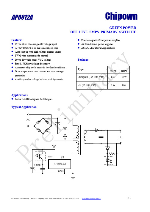
AP8012AChipownGREEN POWEROFF LINE SMPS PRIMARY SWITCHEFeatures●85v to 265v wide range AC voltage input ●A 730v MOSFET on the same silicon chip ●●●●●●●●●Electromagnetic Oven power supplies ●Air Conditioner power supplies ●AC/DC LED Driver ApplicationsPin ConfigurationAbsolute Maximum Ratings(T a=25°C,unless otherwise specified)Symbol Parameter Value Unit V SW SW to GND Voltage(T j=25-125°C)-0.3 (730V)I D Continuous VDMOS Drain Current Internally limited A VCC Supply Voltage0 (50V)I COMP Feedback Current3mAV ESDMM Electrostatic Discharge:Machine Model((R=0Ω;C=200pF)200VV ESDHBM Electrostatic Discharge:HBM2000VT j Junction Operating Temperature Internally limited°CT c Case Operating Temperature-40to150°CT stg Storage Temperature-55to150°C Electrical Characteristic(Power)Symbol Parameter Condition Min.Typ.Max.UnitBV DSS VDMOS Breakdown Voltage I D=1mA;V COMP=2V730750VI DSS Zero Gate Voltage Drain Current V DS=500V;V COMP=2V;100μAR DSON Static Drain-Source on Resistance V GS=10VI D=0.4A;2730ΩT r Rise Time I D=0.1A;V IN=300V50T f Fall Time I D=0.2A;V IN=300V100nsC OSS VDMOS Drain Capacitance V DS=25V40pFElectrical Characteristic(Control)(T a=25°C,VCC=18V,unless otherwise specified)Symbol Parameter Condition Min.Typ.Max.Unit UVLO SECTIONV START VCC Start Threshold Voltage V COMP=0V1415.517V V STOP VCC Stop Threshold Voltage V COMP=0V8910V V HYS VCC Threshold Hysteresis 5.8 6.57.2V OSCILLATOR SECTIONF OSC Initial Accuracy V STOP≤VCC≤35V;0≤T j≤100°C485562kHzΔF/ΔT Frequency Change WithTemperature-25°C≤T j≤+85°C±5±10%FEEDBACK SECTIONI COMP Feedback Shutdown Current Tj=25°C,V COMP=0V0.9mAR COMP COMP Pin Input Impedance ID=0mA 1.4kΩCURRENT LIMIT(SELF-PROTECTION)SECTIONG ID I COMP to I D Current Gain320I LIM Peak Current Limit T j=25°C0.320.400.48A T D Current Sense Delay to Turn-Off I D=0.2A200ns T B Blanking Time500ns T ONMIN Minimum Turn On Time700ns PROTECTION SECTIONT SD Thermal Shutdown Temperature140170-°C T HYST Thermal Shutdown Hysteresis40°C V OVP Over Voltage Protection394347V SUPPLY CURRENT SECTIONI CH Startup Charging Current1mAI CHOFF Start Up Charging Currentin Thermal ShutdownVCC=5V;V DS=100VT j>T SD0.2mAI OP0Operating Supply Current(Control Part Only)SwitchingV COMP=0V4mAI OP1Operating Supply Current(Control Part Only)Not SwitchingV COMP=2V 2.65mAFunctional DescriptionStartupThis device includes a high voltage start up current source connected on the SW of the device.As soon as a voltage is applied on the input of the converter,this start up current source is activated and to charge the VCC capacitor as long as VCC is lower than VSTART.When reaching VSTART,the start up current source is cut off by UVLO&TSD and the device begins to operate by turning on and off its main power MOSFET.As the COMP pin does not receive any current from the opto-coupler,the device operates at full current capacity and the output voltage rises until reaching the regulation point where the secondary loop begins to send a current in the opto-coupler.At this point,the converter enters a regulated operation where the COMP pin receives the amount of current needed to deliver the right power on secondaryside.Fig 1Startup circuit FeedbackA feedback pin controls the operation of the device.Unlike conventional PWM control circuits which use a voltage input,the COMP pin is sensitive to current.Figure 2presents the internal current mode structure.The Power MOSFET delivers a sense current which is proportional to the main current.R2receives this current and the currentcoming from the COMP pin.The voltage across R2VR2isFig 2Feedback Circuitthen compared to a fixed reference voltage.The MOSFETis switched off when VR2equals the reference voltage.Leading Edge Blanking (LEB)At the instant the internal Sense FET is turned on,there usually exists a high current spike through the Sense FET,caused by the primary side capacitance and secondary side rectifier diode reverse recovery.Excessive voltageacross the sense resistor would lead to false feedback operation in the current mode PWM control.To counter this effect,the device employs a leading edge blanking (LEB)circuit.This circuit inhibits the PWM comparator for a short time (typically 500ns)after the Sense FET is turned on.Under Voltage Lock OutOnce fault condition occurs,switching is terminated and the Sense FET remains off.This causes VCC to fall.When VCC reaches the UVLO stop voltage,9V ,the protection is reset and the internal high voltage current source charges the VCC capacitor.When VCC reaches the UVLO start voltage,15.5V ,the device resumes its normal operation.In this manner,the auto-restart can alternately enable and disable the switching of the power Sense FET until the fault condition is eliminated.Thermal Shutdown (TSD)The Sense FET and the control IC are integrated in thesame chip,making it easier for the control IC to detect the temperature of the Sense FET.When the temperature exceeds approximately 170°C,thermal shutdown is activated,the device turn off the Sense FET and the high voltage current source to charge VCC.The device will go back to work when the lower threshold temperature about 140°C is reached.Over Voltage Protection (OVP)In case of malfunction in the secondary side feedback circuit,or feedback loop open caused by a defect of solder,the current through the opto-coupler transistor becomes almost zero.Because excess energy is provided to the output,the output voltage may exceed the rated voltage,resulting in the breakdown of the devices in the secondary side.In order to prevent this situation,an over voltage protection (OVP)circuit is employed.If VCC exceeds 43V ,OVP circuit is activated resulting in termination of the switching operation.In order to avoid undesired activationof OVP during normal operation,VCC should be properly designed to be below43V.Package Dimensions(DIP8)IMPORTANT NOTICEChipown Microelectronics Co.Ltd.reserves the right to make changes without further notice to any products or specifications herein.Chipown Microelectronics Co.Ltd.does not assume any responsibility for use of any its products for any particular purpose,nor does Chipown Microelectronics Co.Ltd assume any liability arising out of the application or use of any its products or circuits.Chipown Microelectronics Co.Ltd does not convey any license under its patent rights or other rights nor the rights of others.8/F,ChuangYuan Building No.21-1Changjiang Road,Wuxi New Destrict Tel:+86(510)8521-7718-8。
A8012中文资料
CLK_I – DO ( CLoad = 100pF )
ENB_I – OUTn
CLK_I – CLK_O LAB_I – LAB_O ENB_I – ENB_O ( CLoad = 100pF )
最小 12.5
5 5 25 25 200
-
-
一般 -
-
-
最大 -
10
50
单位 ns ns ns ns ns ns
输出电流与输出电压关系图
Iout(mA )
40
35
30
25
20
15
10
5
0
0.0
1.0
2.0
3.0
4.0
5.0
6.0
Rext (KΩ)
输出电流与外接电阻关系图 (Iout = 1.23 * 14.5 / Rext)
Ascend Tek, Inc.
Page 8
vsc1.0 Mar 2009
封装外型尺寸: SSOP24
芯片概述
A8012 是专为LED显示应用所设计的恒流 驱动芯片,12个输出通道的电流可由一外 挂电阻调整。每通道最大输出承受电压高 达40V,可串接12颗LED芯片。芯片工作 电压范围宽广,可从5V到24V,串行数据 入/输出的时钟频率可达40MHz。 过温断 电功能则可保护芯片避免在高温环境使用 下而毁损。
符号 VDD VOUT
IDD
VIH VIL VOH VOL IOL IOUT1 ΔIO
ΔIO(2)
ΔIO(3)
Tj RIN-L RIN-H
条件
-
OUT0 ~ OUT11
No data transfer, All outputs OFF
FOD8012评估板用户指南说明书

User Guide forFEBFOD8012_CANEvaluation BoardBi-Directional Logic Gate Optocoupler Provides Proven and Reliable Isolation to the Control Access Network (CAN)InterfaceFeatured Fairchild Product:FOD8012Direct questions or commentsabout this evaluation board to:“Worldwide Direct Support”Fairchild Table of Contents1. Introduction (3)1.1. Description (3)2. Photographs (4)3. Printed Circuit Board (4)3.1. Board Setup and Operation (5)3.2. Test Procedures and Conditions (5)4. Schematic (6)5. Scope Shots (7)6. Conclusion (8)7. Revision History (9)This user guide supports the evaluation board for the FOD8012. It should be used inconjunction with the FOD8012 datasheet as well as Fairchild’s application notes andtechnical support team. Please visit Fairchild’s website at .1.IntroductionThe FOD8012 is an industry-first, full-duplex, bi-directional, logic-gate optocoupler withhigh noise immunity as well as proven and reliable optical isolation. It is highlyintegrated with two optically coupled channels arranged in a bi-directional configurationillustrated in Figure 1. The FOD8012 is housed in a compact 8-pin small-outline package.Each optocoupler channel consists of a high-speed AIGaAs LED driven by a CMOSbuffer IC coupled to a CMOS detector IC.Figure 1. 3-Dimensional Illustration of the Internal Die Set of Fairchild’s Optoplanar®Package Construction1.1.DescriptionThe FOD8012 supports isolated communication between systems of digital signalswithout conducting ground loops or hazardous voltages. Unlike competitive devices,which provide less than 0.1 mm optical isolation gap, the FOD8012 features a 0.4 mm(minimum) optical isolation gap for proven, reliable isolation. The device also features afast switching speed, up to 15 Mbit/s, and uses Fairchild’s Optoplanar® packagingtechnology and optimized IC design to achieve high Common Mode Rejection (CMR) of20 kV/µs minimum, allowing the device to operate in noisy industrial environments.Additionally, the FOD8012 offers an extended industrial temperature range of -40°C to+110ºC and a 3.3 V or 5.0 V supply voltage to facilitate logic level translation. Thedevice’s high isolation voltage is certified by UL1577 and DIN_EN/IEC60747-5-2 forincreased reliability.2.PhotographsThe evaluation includes the FOD8012, a bi-directional logic-gate optocoupler, thatisolates the driver input and receiver output of a half-duplex 5 V CAN transceiver.Figure 2. Photographs of the FEBFOD8012_CAN Board3.Printed Circuit BoardFigure 3. FEBFOD8012_CAN Board Setup3.1.Board Setup and OperationThe FEBFOD8012_CAN evaluation board enables users to make a quick and accurate assessment of Fairchild’s FOD8012 in a bi-directional data transmission application. The setup requires two power supply sources. V DD1 (J1) is on one side of the isolation barrier with V DD2 and V CC (J2) is on the other side of the isolation barrier, sharing the same power supply source. A square wave is applied to one of the FOD8012 channels (VINB / VOB), which in turn drives the CAN transceiver. The resulting CAN output is fed back to the input of the other FOD8012 channel (VINA / VOA). This completes the bi-directional data transmission loop. Test points located at selected positions (as indicated in Figure 3 and Figure 4) allow the user to probe the signals and measure the switching characteristics of the device.3.2.Test Procedures and ConditionsThe following steps and Figure 3 describe the setup of the FEBFOD8012_CAN board.1. Jumpers JP1 and JP2 are connected on the board by default. They connect the CANtransceiver output to the resistive and capacitive loads R2 (60 Ω) and C4 (100 pF),respectively. The user has the flexibility of connecting the CAN driver output /receiver inputs to another load / signal source using the BNC (CANH and CANL)connectors and removing the jumpers (not covered in this document).2. With the power off, connect the power supplies to the board. They are set to3.3 V(J1) or 5.0 V (J2) as specified on the board. Make sure that the supply voltages do notexceed the absolute maximum rating of the devices, as this may damage the device.3. Turn on the power supplies.4. Connect the output of the signal generator to the BNC connector (JR2). The signalgenerator settings are: square wave = 62.5 kHz, duty cycle = 50%, amplitude = 3.3 V,output impedance = 50 Ω.5. Enable the signal generator. The signal waveforms can be probed at various testpoints, as shown in Figure 3:▪TP1: VOA (RX) is the output voltage from channel-A of the FOD8012.▪TP2: VINB (TX) is the input voltage to channel-B of the FOD8012. Signal from the signal generator is applied here.▪TP3: VINA is the input voltage to channel-A of the FOD8012. This signal is supplied by the CAN transceiver.▪TP4: VOB is the output voltage from channel-B of the FOD8012, which in turn drives the input of the CAN transceiver.▪TP5 & TP6: CANH and CANL are the CAN transceivers outputs.▪TP7 to TP10: grounds.4.SchematicThe FEBFOD8012_CAN board is designed to assist evaluation of the FOD8012 timingsequence and AC test performance with a CAN transceiver. It should be used inconjunction with the product datasheet.Figure 4. Evaluation Board Schematic5.Scope ShotsThe scope shots in Figure 5 through Figure 7 illustrate normal operation of the CAN datatransfer via the isolated channels of the FOD8012. Refer to Figure 4 for the schematic.Figure 5. VINB is the Input Signal; FOD8012 Output Signal, VOB, Drives CAN TransceiverFigure 6. FOD8012 Output Signal, VOB, Drives CAN Transceiver; Resulting CAN OutputSignals, CANH and CANL, are Single-Ended Output Signals; V(CANH–CANL) =Differential Output SignalFigure 7. Output Signal from CAN Transceiver Drives Input, VINA, of FOD8012, VOA =FOD8012 Output Signal6.ConclusionThe FEBFOD8012_CAN evaluation board allows the user to evaluate the performance ofthe FOD8012 in a bi-directional data-transmission application with the CAN transceiver.Measurement results clearly demonstrate the high-speed performance of the FOD8012.7.Revision HistoryRev. Date Description1.0.0 August 2012 Initial ReleaseWARNING AND DISCLAIMERReplace components on the Evaluation Board only with those parts shown on the parts list (or Bill of Materials) in the Users’ Guide. Contact an authorized Fairchild representative with any questions.This board is intended to be used by certified professionals, in a lab environment, following proper safety procedures. Use at your own risk. The Evaluation board (or kit) is for demonstration purposes only and neither the Board nor this User’s Guide constitute a sales contract or create any kind of warranty, whether express or implied, as to the applications or products involved. Fairchild warrantees that its products meet Fairchild’s published specifications, but does not guarantee that its products work in any specific application. Fairchild reserves the right to make changes without notice to any products described herein to improve reliability, function, or design. Either the applicable sales contract signed by Fairchild and Buyer or, if no contract exists, Fairchild’s standard Terms and Conditions on the back of Fairchild invoices, govern the terms of sale of the products described herein. DISCLAIMERFAIRCHILD SEMICONDUCTOR RESERVES THE RIGHT TO MAKE CHANGES WITHOUT FURTHER NOTICE TO ANY PRODUCTS HEREIN TO IMPROVE RELIABILITY, FUNCTION, OR DESIGN. FAIRCHILD DOES NOT ASSUME ANY LIABILITY ARISING OUT OF THE APPLICATION OR USE OF ANY PRODUCT OR CIRCUIT DESCRIBED HEREIN; NEITHER DOES IT CONVEY ANY LICENSE UNDER ITS PATENT RIGHTS, NOR THE RIGHTS OF OTHERS.LIFE SUPPORT POLICYFAIRCHILD’S PRODUCTS ARE NOT AUTHORIZED FOR USE AS CRITICAL COMPONENTS IN LIFE SUPPORT DEVICES OR SYSTEMS WITHOUT THE EXPRESS WRITTEN APPROVAL OF THE PRESIDENT OF FAIRCHILD SEMICONDUCTOR CORPORATION.As used herein:1. Life support devices or systems are devices or systems which, (a)are intended for surgical implant into the body, or (b) support orsustain life, or (c) whose failure to perform when properly used in accordance with instructions for use provided in the labeling, can be reasonably expected to result in significant injury to the user. 2. A critical component is any component of a life support device orsystem whose failure to perform can be reasonably expected to cause the failure of the life support device or system, or to affect its safety or effectiveness.ANTI-COUNTERFEITING POLICYFairchild Semiconductor Corporation's Anti-Counterfeiting Policy. Fairchild's Anti-Counterfeiting Policy is also stated on our external website, , under Sales Support.Counterfeiting of semiconductor parts is a growing problem in the industry. All manufacturers of semiconductor products are experiencing counterfeiting of their parts. Customers who inadvertently purchase counterfeit parts experience many problems such as loss of brand reputation, substandard performance, failed applications, and increased cost of production and manufacturing delays. Fairchild is taking strong measures to protect ourselves and our customers from the proliferation of counterfeit parts. Fairchild strongly encourages customers to purchase Fairchild parts either directly from Fairchild or from Authorized Fairchild Distributors who are listed by country on our web page cited above. Products customers buy either from Fairchild directly or from Authorized Fairchild Distributors are genuine parts, have full traceability, meet Fairchild's quality standards for handling and storage and provide access to Fairchild's full range of up-to-date technical and product information. Fairchild and our Authorized Distributors will stand behind all warranties and will appropriately address any warranty issues that may arise. Fairchild will not provide any warranty coverage or other assistance for parts bought from Unauthorized Sources. Fairchild is committed to combat this global problem and encourage our customers to do their part in stopping this practice by buying direct or from authorized distributors.EXPORT COMPLIANCE STATEMENTThese commodities, technology, or software were exported from the United States in accordance with the Export Administration Regulations for the ultimate destination listed on the commercial invoice. Diversion contrary to U.S. law is prohibited.U.S. origin products and products made with U.S. origin technology are subject to U.S Re-export laws. In the event of re-export, the user will be responsible to ensure the appropriate U.S. export regulations are followed.Mouser ElectronicsAuthorized DistributorClick to View Pricing, Inventory, Delivery & Lifecycle Information:F airchild Semiconductor:FOD8012FEBFOD8012_CAN。
LIS8410C_Datasheet _V1.0

版权© 莱士电子科技有限公司
莱士电子科技有限公司
4/7
LIS-DS-8410C-V1.0
LIS8410C
非隔离降压式 LED 驱动控制器
功能描述
启动和供电 LIS8410C 是通过供电电阻从线电压直接启动。通 过典型应用电路可以了解到,当采用这种供电方式 启动时,芯片 VDD 的供电电容首先通过供电电阻由 线电压充电,当其上的电压达到阈值 UVLO(off)后, 芯片启动,并开始输出脉冲驱动内部功率开关,由 于芯片自身的耗电非常少,通过启动电阻供电,便 可使 VDD 电压维持在某一值上,保证 IC 正常工作。
变压器匝数计算 当以上计算,得出L和IPK后,需用到NBS=LIPK来计算 出变压器或电感的最少匝数,N>LIPK/BS;N为变压 器线圈匝数, S为变压器磁芯中柱的截面积(AE值), B的取值需参考磁芯材质而定,以PC40材质为例,建 议B取值0.28T以下。
最短消磁时间与最长消磁时间 LIS8410C 设置了最短消磁时间和最长消磁时间,当 电感过小或输出电压过高时(输出开路),电感的消 磁时间就有可能小于芯片的最短消磁时间,此时芯片 进入保护状态,系统不断重启;当电感过大或输出电 压过低时(输出短路),电感的消磁时间就有可能大 于芯片的最长消磁时间,此时芯片也会进入保护状态。 因此选取一个合理的电感值非常重要,需要设计者重 点考量。需特别指出,当电源正常工作时,其设计的 最小消磁时间一定不能小于芯片的最小消磁时间,并 且留有足够的余量,否则电源将不能正常工作,由于 该系统架构是降压式,所以输入端整流后的最小直流 电压也一定不能低于输出电压。
过温保护 LIS8410C 集成了过温保护功能,当芯片温度超过 保护阈值后,开关管会关断,进入自动重起保护模 式。当错误条件消失,系统自动恢复正常工作状态。
28130;中文规格书,Datasheet资料
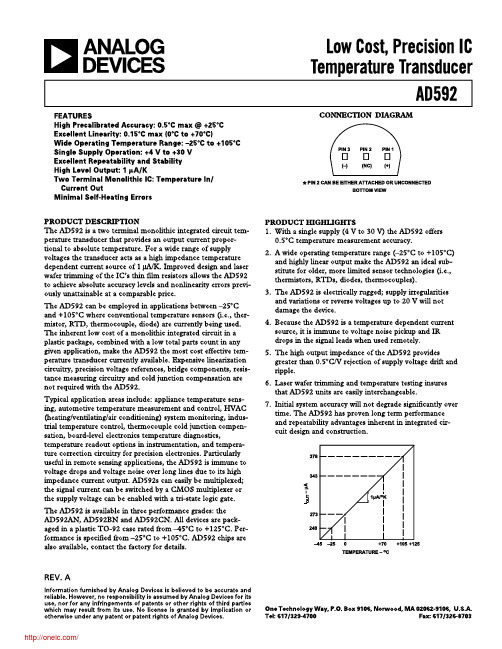
METALIZATION DIAGRAM
TEMPERATURE SCALE CONVERSION EQUATIONS
+2.0 +1.5 +1.0 +0.5
0 –0.5 –1.0 –1.5 –2.0
–25
0
+25
+70
TEMPERATURE – oC
+105
AD592BN Accuracy Over Temperature
TOTAL ERROR – oC TOTAL ERROR – oC
+2.0 +1.5 +1.0 +0.5
+1.0
+0.5
MAXIMUM ERROR OVER TEMPERATURE
TYPICAL ERROR
0 CALIBRATION ERROR LIMIT
–0.5
TOTAL ERROR – oC
IOUT – µA
378
+105oC
298
+25oC
–25oC 248
UP TO 30V
0
1
2
3
4
5
6
SUPPLY VOLTAGE – Volts
66MILS
V+
V–
/
Model
AD592CN AD592BN AD592AN
42MILS
؇C = 5 (؇F –32) 9
PMAC801产品说明书V3.1

第 6 章 显示模块 ................................................................................................17
6.1 描述 ........................................................................................................................................... 17 6.2 主要功能................................................................................................................................... 18
Fiberxon FTM-8012S-GG 1.0625-1.25Gbps GBIC Transce
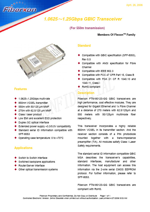
April. 26, 20061.0625~1.25Gbps GBIC TransceiverMembers Of Flexon TM FamilyFeaturesDuplex SC optical interfaceExtended power supply +3.3/5.0V compatibility Standard serial ID information compatible withSFF-8053Operating case temperature: 0 to +70°CApplicationsSwitch to Switch interface Switched backplane applications Router/Server interface Other optical transmission systemsStandardCompatible with GBIC specification (SFF-8053),Rev 5.5Compatible with ANSI specification for FibreChannelCompatible with IEEE 802.3550 meters with 50/125µm multimode fiber respectively.This transceiver incorporates a highly reliable 850nm VCSEL in its transmitter section. And the receiver section consists of a PIN photodiode mounted together with a trans-impedance preamplifier (TIA). All modules satisfy Class I Laser Safety requirements.The standard serial ID information compatible GBIC MSA describes the transceiver’s capabilities, standard interfaces, manufacturer and other information. The host equipment can access this information via the 2-wire serial CMOS EEPROM protocol. For further information, please refer to SFF-8053.Fiberxon FTM-8012S-GG GBIC transceivers are compliant with RoHS. Fiberxon Proprietary and Confidential, Do Not Copy or Distribute Page 1 of 1Regulatory ComplianceThe transceivers have been tested according to American and European product safety and electromagnetic compatibility regulations (See Table 1). For further information regarding regulatory certification, please referto Flexon TM regulatory specification and safety guidelines, or contact with Fiberxon, Inc. America sales officelisted at the end of the documentation.Absolute Maximum Ratings are those values beyond which damage to the devices may occur.Table 2 – Absolute Maximum RatingsParameter Symbol Min. Max. UnitStorage Temperature T S-40 +85 °C Supply Voltage V CC-0.5 6 V Operating Humidity - 5 95 %Recommended Operating ConditionsTable 3 - Recommended Operating ConditionsParameter Symbol Min. Typical Max. Unit°C Operating Case Temperature T C0 +70Power Supply Voltage V CC 3.1 5.5 VmA Power Supply Current I CC300Data Rate 1.0625/1.25GbpsFTM-8012S-GGNotes:1. The optical power is launched into MMF.2. Unfiltered, measured with a PRBS 27**********************3. Meet the specified maximum output jitter requirements if the specified maximum input jitter is present.4. Measured with a PRBS 27**********************/1.0625Gbps.5. PECL logic, internally AC coupled.6. Measured with a PRBS 27**********************,worst-caseextinctionratio,BER≤1×10-12.EEPROM InformationThe SFF-8053 defines a 256-byte memory map in EEPROM describing the transceiver’s capabilities, standard interfaces, manufacturer, and other information, which is accessible over a 2 wire serial interface at the 8-bit address 1010000X (A0h). The memory contents refer to Table 5Note: The “xx” byte should be filled in according to practical case. For more information, please refer to the related document of SFF-8053 Rev 5.5.Recommended Interface CircuitFigure 1 shows the recommended interface circuit.Figure 1, Recommended Interface CircuitPin DefinitionsFigure 2 below shows the pin numbering of GBIC electrical interface. The pin functions are described in Table 6.Figure 2, Pin ViewMechanical Design DiagramThe mechanical design diagram is shown in Figure 3.Ordering information8: 850nm Function 0:Standard Data rate12: 1.25G/1.0625GS: SCOthersG: RoHS compliancePart No. Product DescriptionFTM-8012S-GG850nm, 1.0625~1.25Gbps, 550m, GBIC, RoHS compliant, 0°C~+70°CRelated DocumentsFor further information, please refer to the following documents:Flexon TM GBIC Installation GuideFlexon TM GBIC Application NotesSFF-8053, Proposed Specification for GBIC (Gigabit Interface Converter), Rev 5.5Obtaining DocumentYou can visit our website:TOr contact with Fiberxon, Inc. America Sales Office listed at the end of documentation to get the latestAll information contained in this document is subject to change without notice. The products described in this document are NOT intended for use in implantation or other life support applications where malfunction may result in injury or death to persons.The information contained in this document does not affect or change Fiberxon’s product specifications or warranties. Nothing in this document shall operate as an express or implied license or indemnity under the intellectual property rights of Fiberxon or third parties. All information contained in this document was obtained in specific environments, and is presented as an illustration. The results obtained in other operating environment may vary.THE INFORMATION CONTAINED IN THIS DOCUMENT IS PROVIDED ON AN ”AS IS” BASIS. In no event will Fiberxon be liable for damages arising directly from any use of the information contained in this document. ContactU.S.A. Headquarter:5201 Great America Parkway, Suite 340Santa Clara, CA 95054U. S. A.Tel: 408-562-6288Fax: 408-562-6289Or visit our website: 。
IC资料-AP8012技术资料

GREEN POWEROFF LINE SMPS PRIMARY SWITCHEFeatures●85v to 265v wide range AC voltage input ●A 730v MOSFET on the same silicon chip ●Auto start up with high voltage current source ●PWM with current mode control ●10v to 39v wide range VCC voltage ●Fixed 55KHz switching frequency●Automatic skip cycle mode in low load condition.●Over temperature,over current and over voltage protection●Auxiliary under voltage lockout with hysteresisApplications●Power AC/DC Adapters for Chargers●Electromagnetic Oven power supplies ●Air Conditioner power supplies ●AC/DC LED Driver ApplicationsPackageTypeSOP8DIP8European (195-265Vac)8W 13W US (85-265Vac)5W8WTypicalApplicationPin ConfigurationAbsolute Maximum Ratings(T a=25°C,unless otherwise specified)Symbol Parameter Value Unit V SW SW to GND Voltage(T j=25-125°C)-0.3 (730V)I D Continuous VDMOS Drain Current Internally limited A VCC Supply Voltage0 (50V)I COMP Feedback Current3mAV ESDMM Electrostatic Discharge:Machine Model((R=0Ω;C=200pF)200VV ESDHBM Electrostatic Discharge:HBM2000VT j Junction Operating Temperature Internally limited°CT c Case Operating Temperature-40to150°CT stg Storage Temperature-55to150°C Electrical Characteristic(Power)Symbol Parameter Condition Min.Typ.Max.UnitBV DSS VDMOS Breakdown Voltage I D=1mA;V COMP=2V730750VI DSS Zero Gate Voltage Drain Current V DS=500V;V COMP=2V;100μAR DSON Static Drain-Source on Resistance V GS=10VI D=0.4A;2730ΩT r Rise Time I D=0.1A;V IN=300V50T f Fall Time I D=0.2A;V IN=300V100nsC OSS VDMOS Drain Capacitance V DS=25V40pFElectrical Characteristic(Control)(T a=25°C,VCC=18V,unless otherwise specified)Symbol Parameter Condition Min.Typ.Max.Unit UVLO SECTIONV START VCC Start Threshold Voltage V COMP=0V1415.517V V STOP VCC Stop Threshold Voltage V COMP=0V8910V V HYS VCC Threshold Hysteresis 5.8 6.57.2V OSCILLATOR SECTIONF OSC Initial Accuracy V STOP≤VCC≤35V;0≤T j≤100°C485562kHzΔF/ΔT Frequency Change WithTemperature-25°C≤T j≤+85°C±5±10%FEEDBACK SECTIONI COMP Feedback Shutdown Current Tj=25°C,V COMP=0V0.9mAR COMP COMP Pin Input Impedance ID=0mA 1.4kΩCURRENT LIMIT(SELF-PROTECTION)SECTIONG ID I COMP to I D Current Gain320I LIM Peak Current Limit T j=25°C0.320.400.48A T D Current Sense Delay to Turn-Off I D=0.2A200ns T B Blanking Time500ns T ONMIN Minimum Turn On Time700ns PROTECTION SECTIONT SD Thermal Shutdown Temperature140170-°C T HYST Thermal Shutdown Hysteresis40°C V OVP Over Voltage Protection394347V SUPPLY CURRENT SECTIONI CH Startup Charging Current1mAI CHOFF Start Up Charging Currentin Thermal ShutdownVCC=5V;V DS=100VT j>T SD0.2mAI OP0Operating Supply Current(Control Part Only)SwitchingV COMP=0V4mAI OP1Operating Supply Current(Control Part Only)Not SwitchingV COMP=2V 2.65mAFunctional DescriptionStartupThis device includes a high voltage start up current source connected on the SW of the device.As soon as a voltage is applied on the input of the converter,this start up current source is activated and to charge the VCC capacitor as long as VCC is lower than VSTART.When reaching VSTART,the start up current source is cut off by UVLO&TSD and the device begins to operate by turning on and off its main power MOSFET.As the COMP pin does not receive any current from the opto-coupler,the device operates at full current capacity and the output voltage rises until reaching the regulation point where the secondary loop begins to send a current in the opto-coupler. At this point,the converter enters a regulated operation where the COMP pin receives the amount of currentneeded to deliver the right power on secondaryside.Fig1Startup circuitFeedbackA feedback pin controls the operation of the device.Unlike conventional PWM control circuits which use a voltage input,the COMP pin is sensitive to current.Figure2 presents the internal current mode structure.The Power MOSFET delivers a sense current which is proportional to the main current.R2receives this current and the current coming from the COMP pin.The voltage across R2VR2isFig2Feedback Circuitthen compared to a fixed reference voltage.The MOSFET is switched off when VR2equals the reference voltage. Leading Edge Blanking(LEB)At the instant the internal Sense FET is turned on,there usually exists a high current spike through the Sense FET, caused by the primary side capacitance and secondary side rectifier diode reverse recovery.Excessive voltage across the sense resistor would lead to false feedback operation in the current mode PWM control.To counter this effect,the device employs a leading edge blanking (LEB)circuit.This circuit inhibits the PWM comparator for a short time(typically500ns)after the Sense FET is turned on.Under Voltage Lock OutOnce fault condition occurs,switching is terminated and the Sense FET remains off.This causes VCC to fall.When VCC reaches the UVLO stop voltage,9V,the protection is reset and the internal high voltage current source charges the VCC capacitor.When VCC reaches the UVLO start voltage,15.5V,the device resumes its normal operation.In this manner,the auto-restart can alternately enable and disable the switching of the power Sense FET until the fault condition is eliminated.Thermal Shutdown(TSD)The Sense FET and the control IC are integrated in the same chip,making it easier for the control IC to detect the temperature of the Sense FET.When the temperature exceeds approximately170°C,thermal shutdown is activated,the device turn off the Sense FET and the high voltage current source to charge VCC.The device will go back to work when the lower threshold temperature about 140°C is reached.Over Voltage Protection(OVP)In case of malfunction in the secondary side feedback circuit,or feedback loop open caused by a defect of solder, the current through the opto-coupler transistor becomes almost zero.Because excess energy is provided to the output,the output voltage may exceed the rated voltage, resulting in the breakdown of the devices in the secondary side.In order to prevent this situation,an over voltage protection(OVP)circuit is employed.If VCC exceeds43V, OVP circuit is activated resulting in termination of the switching operation.In order to avoid undesiredactivationof OVP during normal operation,VCC should be properly designed to be below43V. Reference CircuitPackage Dimensions(DIP8)IMPORTANT NOTICEChipown Microelectronics Co.Ltd.reserves the right to make changes without further notice to any products or specifications herein.Chipown Microelectronics Co.Ltd.does not assume any responsibility for use of any its products for any particular purpose,nor does Chipown Microelectronics Co.Ltd assume any liability arising out of the application or use of any its products or circuits.Chipown Microelectronics Co.Ltd does not convey any license under its patent rights or other rights nor the rights of others.8/F,ChuangYuan Building No.21-1Changjiang Road,Wuxi New Destrict Tel:+86(510)8521-7718-8。
AP8012C Datasheet中文版Rev B 1301
0.17
—
0.25
0.17
0.20
0.23
4.80
4.90
5.00
5.80
6.00
6.20
3.80
3.90
4.00
1.270(BSC)
尺寸 符号
L L1 L2 R R1 h θ θ1 θ2 θ3 θ4
图 2. 外形示意图
最小 (mm) 0.45
0.07 0.07 0.30 0° 15° 11° 15° 11°
2. 软启动
图 3 启动电路
启动阶段,漏极的最大峰值电流限制逐步的提高;可以大大减小器件的应力,防止变压器饱和。软启动
时间典型值为8ms。
3. 输出驱动
AP8012C采用特有的驱动技术。驱动能力太弱会使得较高的开关损耗,驱动太强则容易出现EMI问题。 AP8012C采用优化的图腾柱结构,通过合理的输出驱动能力以及死区时间,得到较好的EMI特性和较低的损 耗。
正常 (mm) 0.60 1.04REF 0.25BSC
— — 0.40 — 17° 13° 17° 13°
AP8012C
最大 (mm) 0.80
— — 0.50 8° 19° 15° 19° 15°
表层丝印
封装
AP8012C
DIP8
YWWXXXXX
SOP8
备注:Y:年份代码; W:周代码; XXXXX:内部代码
J
CC
表 3. 功率部分
符号 BVDSS RDSON
参数 功率管耐压 功率管导通电阻
AP8012C
测试条件 T =125°C
J
VGS=10V;ID=0.2 A;
最小 700
典型
AP8012替换Viper12A应用说明
AP8012替换Viper12A应用说明AP8012替换Viper12A应用说明AP8012可PIN TO PIN替换V iper12A。
由于AP8012在个别电参数上与Viper12A存有差异性,所以在某些反激式电源系统方案上做直接替换需注意到一些系统参数的调整,以最优化的方式使用AP8012。
1.性能参数差异点:序号主要区别AP8012 VIPER121 启动电压典型值DC15.5V DC14.5V2 关断电压典型值DC9V DC8V3 内置MOS管最小值730V,典型值750V 最小值730V,典型值800V4 VCC工作电流典型值4mA 4.5mA5 工作频率典型值55kHz 60kHz2.应用分析及优化条件:序号参数差异分析需要调整的器件器件调整值1 启动电压高对系统应用基本没有影响。
无2 由于关断电压高,实际应用的时候,在电源空载的情况下,VCC电源会降低,如果电压降低到9V以下,会引起芯片当机重启。
变压器将辅助绕组端的输出电压设置在12V,确保空载的时候电压不会低于9V。
3 内置MOS耐压低,在浪涌、老化、启动、短路的时侯都会有高压引入,造成MOS击穿。
变压器RC吸收电路变压器调整参看后面建议,RC参数建议C=10NF、R=51K。
4 工作电流少,对系统应用没影响,不做修改。
无5 工作频率比VIPER低5kHz,所以变压器更容易饱和,饱和后的芯片温度也更高变压器变压器调整参看后面建议。
变压器参数分析:为了确保MOS不被击穿,同时变压器不出现饱和现象,我们推荐一下数值:变压器规格建议初级圈数建议感量建议初级与次级匝比输出3.3V 输出5V 输出9V 输出12VEE16 140~160T 2.7~3.3mH 16:1 14:1 8:1 6.15:1 EE19 110~130T 2.7~3.3mH 16:1 14:1 8:1 6.15:1 EE20 110~130T 2.7~3.3mH 16:1 14:1 8:1 6.15:1 EE22 100~120T 2.7~3.3mH 16:1 14:1 8:1 6.15:1 EF25 90~110T 2.7~3.3mH 16:1 14:1 8:1 6.15:1 EE28 90~110T 2.7~3.3mH 16:1 14:1 8:1 6.15:1 注:初级的反射电压控制在80V以下。
FEELINGTECH--FP8012芯片--翻译(DOC)

SOP8E封装的1A线性锂电池充电模块总述FP8012是一个SOP8封装的独立锂电池充电芯片,它的外部器件很少,且可对大部分的移动设备充电。
充电电流可以由外部电阻来控制。
在待机模式中,提供的电流可以减小至55μA。
它还具有UVLO,自动再充,充电状态显示和发热调节等功能。
特征是单块锂电池的独立充电器不需要外部MOSFET、检测电阻和限流二极管最大1A的可编程充电电流预设定的充电电压精度达到±1%自动再充2.9V的细流充电电压C/10时充电终止55 μA的待机电流可以指示没有电池或者充电失败小电流启动充电以防止电流冲击过热保护应用场合便携式信息设备充电底座手机或者PDA掌上电脑典型的应用电路功能模块图充电状态指示状态图引脚功能商标的含义无卤:产品不含卤的标示批号:晶片批号的最后两位数字例如:132386TB→86内部编码:内部的识别号每半个月:以半个月作为生产周期的标示例如:1月—→A(上半月),B(下半月)2月—→C(上半月),D(下半月)年:出产那年的最后一个数字订购信息绝对最大额定值推荐的应用环境直流电气特性待机模式,,V BAT上升,电流模式从高到低典型的应用特性(无特殊标明时,)功能描述操作FP8012最初是为单块锂电池充电而设计的线性电池充电器。
它采用恒定的电流或电压算法而且电流是可编程控制的。
充电电流根据外部的单块限流电阻来控制。
FP8012包含内部P通道的MOSFET和热控电路。
不需要限流二极管或者外部检测电阻。
因此,最基本的充电电路只需要两个外部组件。
此外,FP8012适用于由USB供电运行。
常规充电循环过程当Vcc引脚电压大于UVLO设定的阈值则开始充电。
如果BA T引脚的电压小于2.9V,则进入小电流充电模式,在这种模式下,FP8012输出的电流大约为设定电流的1/10进行充电直至充电完成。
当BAT引脚电压大于2.9V时,则输出以设定电流为准的恒流充电模式。
当BAT的引脚电压达到4.2V时,则进入恒压充电模式,此时充电电流开始减小,当充电电流减小到设定电流值的1/10时,充电循环终止。
- 1、下载文档前请自行甄别文档内容的完整性,平台不提供额外的编辑、内容补充、找答案等附加服务。
- 2、"仅部分预览"的文档,不可在线预览部分如存在完整性等问题,可反馈申请退款(可完整预览的文档不适用该条件!)。
- 3、如文档侵犯您的权益,请联系客服反馈,我们会尽快为您处理(人工客服工作时间:9:00-18:30)。
Rev.B.1301
4/8
AP8012C
功能描述
1. 启动 AP8012C 内部集成高压启动电路,启动时 SW 脚对 VCC 电源提供充电电流。当 VCC 电压达到 VSTART
电压时,内部高压启动电路关闭,VCC 电容的能量由变换器提供;一旦 VCC 电压低于欠压保护点,高压启 动管开启并为 VCC 电容充电,直至 VCC 电压达到 VSTART。
4. 振荡器
AP8012C的振荡频率固定在60 kHz,无需外围电路进行设置。它含有特有的频率抖动技术,可以改善 EMI特性。
5. 反馈回路
反馈脚通过控制 MOSFET 的开通和关断实现输出的稳定。不同于传统的电压模式 PWM 控制电路, AP8012C 采用电流控制方式(如图 4 所示),通过内部采样管得到流过功率 MOS 的电流。从 COMP 脚流入 的电流通过 R2 进行采样,采样电压(VR2))跟内部基准 VR2 比较;当 VR2 的电压超过内部基准电压时, 则关断 MOSFET 实现环路的控制。
IDD VCC VCCclamp VCCovp IDD_OFF
工作电流 工作电压范围 VCC箝位电压 VCC过压保护电压 VCC < VCC_OFF工作电流
VDRAIN = 120 V, VCOMP = GND, VCC = 4 V VDRAIN = 120 V After turn-on IDD = 5mA
由于SW脚的寄生电容,当MOS开通瞬间存在较大的峰值电流,如果采样MOSFET采样到该信号,芯片 会过入过流保护状态。为了防止MOS开通瞬间引起电路误触发,过流保护电路在功率管开通一段时间(典 型值300ns)后才开始工作。
7. 欠压锁定 由于异常情况导致功率管被关闭后,VCC脚电压由于没有提供能量将会一直下降,当VCC电压下降到
0.17
—
0.25
0.17
0.20
0.23
4.80
4.90
5.00
5.80
6.00
6.20
3.80
3.90
4.00
1.270(BSC)
尺寸 符号
L L1 L2 R R1 h θ θ1 θ2 θ3 θ4
图 2. 外形示意图
最小 (mm) 0.45
0.07 0.07 0.30 0° 15° 11° 15° 11°
A A1 A2 A3 A4 A5 B C C1
图 5. 外形示意图
最小(mm) 9.30
最大(mm) 9.50
尺寸 符号
C2
1.524
C3
0.39
0.53
C4
2.54
D
0.66TYP
D1
0.99TYP
D2
6.3
6.5
Θ1
7.2
Θ2
3.3
3.5
Θ3
AP8012C
最小(mm)
最大(mm)
0.50
3.3
1.57TYP
最小
典型
最大
单位
VCOMP=0V VCOMP=0V
12
13.2
14.5
V
8.2
9
9.8
V
4
V
0≤TA≤ 100°C
54
60
66
kHz
±4
kHz
250
Hz
60
90
%
1.1
mA
1.3
kΩ
TA = 25°C LEB time
VCOMP= 0.6 V
0.38
0.44
0.5
A
300
ns
9.6
ms
100
mA
140ห้องสมุดไป่ตู้
J
CC
表 3. 功率部分
符号 BVDSS RDSON
参数 功率管耐压 功率管导通电阻
AP8012C
测试条件 T =125°C
J
VGS=10V;ID=0.2 A;
最小 700
典型
最大 30
单位 V Ω
表 4. 控制部分
符号
参数
欠压保护部分
VSTART
欠压保护启动电压
VSTOP
欠压保护关断电压
VHYS
欠压保护回差
GND
AP8012C
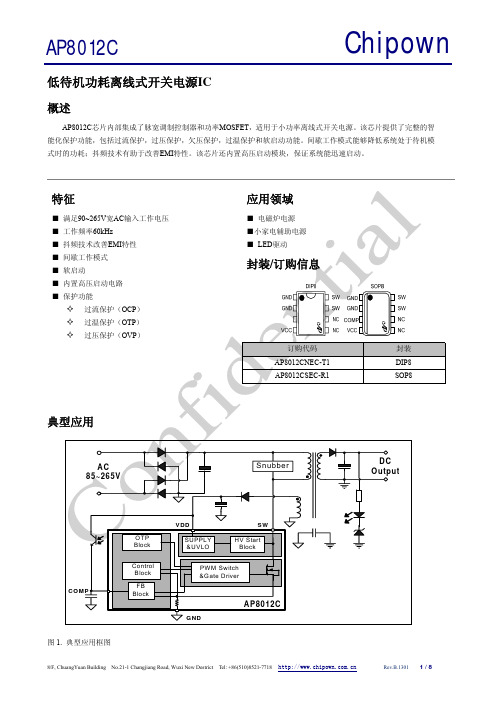
图 1. 典型应用框图
8/F, ChuangYuan Building No.21-1 Changjiang Road, Wuxi New Destrict Tel: +86(510)8521-7718
Rev.B.1301 1 / 8
8/F, ChuangYuan Building No.21-1 Changjiang Road, Wuxi New Destrict Tel: +86(510)8521-7718
Rev.B.1301
8/8
VCC = 7 V
典型应用
AP8012C
-1
mA
1
mA
9.9
24
V
26.3
28.3
30.3
V
24.3
26.3
28.3
V
350
uA
图 2. 应用典型线路
8/F, ChuangYuan Building No.21-1 Changjiang Road, Wuxi New Destrict Tel: +86(510)8521-7718
Rev.B.1301
7/8
表 6. SOP-8 封装尺寸
尺寸 符号
A A1 A2 A3 b b1 c c1 D E E1 e
最小
正常
最大
(mm)
(mm)
(mm)
1.35
1.55
1.75
0.10
0.15
0.25
1.25
1.40
1.65
0.50
0.60
0.70
0.38
—
0.51
0.37
0.42
0.47
AP8012C
管脚定义
表 1. 管脚定义
管脚标号 1,2 3
4 5,6 7,8
管脚名 GND COMP
VCC
NC SW
管脚功能描述 功率MOS以及控制电路的参考地 反馈输入脚,用以确定功率MOS的峰值电流 控制电路的供电电源,启动时由高压启动管对VCC电容进行充 电,当达到UVLO启动电压时,启动过程结束。 空脚。 功率MOS的漏极。
欠压锁定保护点(典型值9V)时,欠压锁定电路被复位,内部高压电流源重新开始给VCC提供能量。直至 VCC电压上升到欠压锁定解除点(典型值13.2V)时,芯片开始正常工作,功率管正常开启和关闭。通过这 种控制方法,芯片在异常情况消除后能自动重启动。
8. 过温保护
功率MOSFET和控制芯片集成在一起,能保证温度采样电路更准确的采样功率管的温度信号,从而更及 时的对功率管进行保护。当芯片结温超过170℃时(典型值),芯片进入过温保护状态;直至结温回到140℃ (典型值)时,芯片重新开始工作。温度保护存在滞回,保证芯片不会出现热振荡现象。
图 4 反馈电路
8/F, ChuangYuan Building No.21-1 Changjiang Road, Wuxi New Destrict Tel: +86(510)8521-7718
Rev.B.1301
5/8
AP8012C
6. 前沿消隐
正常 (mm) 0.60 1.04REF 0.25BSC
— — 0.40 — 17° 13° 17° 13°
AP8012C
最大 (mm) 0.80
— — 0.50 8° 19° 15° 19° 15°
表层丝印
封装
AP8012C
DIP8
YWWXXXXX
SOP8
备注:Y:年份代码; W:周代码; XXXXX:内部代码
典型功率
表 2. 典型功率
测试条件
90~265 VAC DIP8
Flyback /55℃
5W
备注:最大连续功率在开放环境且有足够散热条件下测试
90~265 VAC SOP8 3.6W
极限工作范围
VCC 工作电压范围 ……………………………………………………….…. -0.3~30V SW 脚最高电压 …………………………………………………………….…700V 上电时启动管最高电压………………………………………………………-0.3~400V 反馈脚最大电流…………………………………………………………………1.2mA 高压功率管电流………………………………………………………………Internally limited 机械模式 ESD 能力……………………………………………. ………………200V 结工作温度……………………………………………………………………Internally limited 工作温度范围…………………………………………………………………-40~150℃ 存储温度范围…………………………………………………………………-55~150℃ 管脚焊接温度 (10秒) …………………………………………………………260℃
2. 软启动
图 3 启动电路
启动阶段,漏极的最大峰值电流限制逐步的提高;可以大大减小器件的应力,防止变压器饱和。软启动
时间典型值为8ms。
3. 输出驱动
AP8012C采用特有的驱动技术。驱动能力太弱会使得较高的开关损耗,驱动太强则容易出现EMI问题。 AP8012C采用优化的图腾柱结构,通过合理的输出驱动能力以及死区时间,得到较好的EMI特性和较低的损 耗。
8/F, ChuangYuan Building No.21-1 Changjiang Road, Wuxi New Destrict Tel: +86(510)8521-7718
