DS1302部分中文翻译
DS1302数据手册翻译
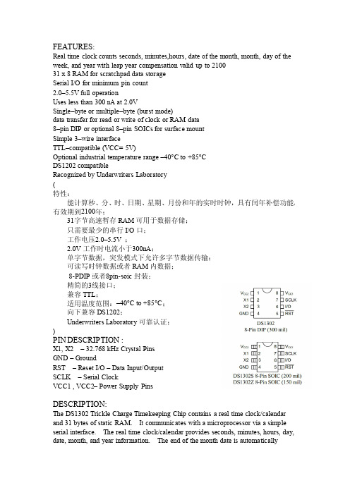
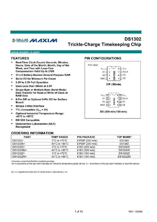
Real time clock counts seconds, minutes,hours, date of the month, month, day of the week, and year with leap year compensation valid up to 2100 31 x 8 RAM for scratchpad data storage Serial I/O for minimum pin count 2.0–5.5V full operation Uses less than 300 nA at 2.0V Single–byte or multiple–byte (burst mode) data transfer for read or write of clock or RAM data 8–pin DIP or optional 8–pin SOICs for surface mount Simple 3–wire interface TTL–compatible (VCC= 5V) Optional industrial temperature range –40°C to +85°C DS1202 compatible Recognized by Underwriters Laboratory ( 特性:
SIGNAL DESCRIPTIONS VCC1– VCC1 provides low power operation in single supply and battery operated
systems as well as low power battery backup. In systems using the trickle charger, the rechargeable energy source is connected to this pin.
DS1302中文资料
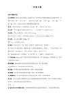
VVcccc11:主电源;VVcccc22:备份电源。当VVcccc22>>VVcccc11++00..22VV时,由VVcccc22
DS1302 Vcc2<Vcc1 Vcc1 DS1302
能力。
----------------------- Page 9-----------------------
DS1302动程序分析
开 始
CCLLKK和和II//OO虽虽然然和和IIIICC总总线线接接在在一一条条引引脚脚上上,,但但DDSS11330022其其实实并并不不是是
使用IIC总线,而是一种三线式总线,
使用IIC总线,而是一种三线式总线,
使使用用IIIICC总总线线,,而而是是一一种种三三线线式式总总线线,,
Vcc2>Vcc1+0.2V 时,
Vcc2>Vcc1+0.2V 时,
VVcccc22>>VVcccc11++00..22VV时时,,
由 Vcc2向 DS1302供电,当 Vcc2<Vcc1时,由 Vcc1向
由 Vcc2向 DS1302供电,当 Vcc2<Vcc1时,由 Vcc1向
I/O 数据输入/输出引脚
SCLK 串行时钟
Vcc1,Vcc2电源供电管脚
各引脚的功能为
各引脚的功能为
各各引引脚脚的的功功能能为为:
Vcc1 Vcc2 Vcc2>Vcc1+0.2V Vcc2
----------------------- Page 3-----------------------
外文翻译--DS1302涓流充电计时芯片
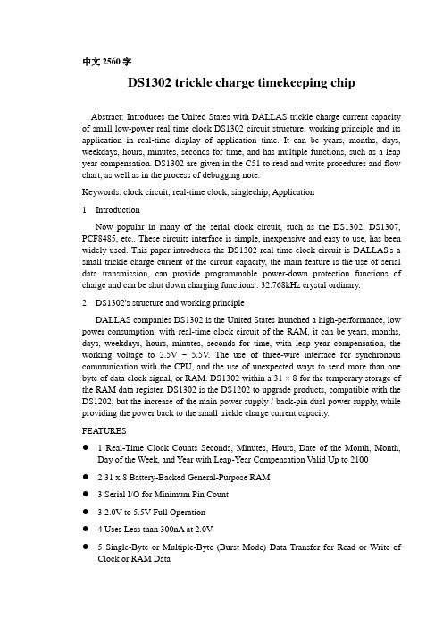
中文2560字DS1302 trickle charge timekeeping chip Abstract: Introduces the United States with DALLAS trickle charge current capacity of small low-power real time clock DS1302 circuit structure, working principle and its application in real-time display of application time. It can be years, months, days, weekdays, hours, minutes, seconds for time, and has multiple functions, such as a leap year compensation. DS1302 are given in the C51 to read and write procedures and flow chart, as well as in the process of debugging note.Keywords: clock circuit; real-time clock; singlechip; Application1 IntroductionNow popular in many of the serial clock circuit, such as the DS1302, DS1307, PCF8485, etc.. These circuits interface is simple, inexpensive and easy to use, has been widely used. This paper introduces the DS1302 real time clock circuit is DALLAS's a small trickle charge current of the circuit capacity, the main feature is the use of serial data transmission, can provide programmable power-down protection functions of charge and can be shut down charging functions . 32.768kHz crystal ordinary.2 DS1302's structure and working principleDALLAS companies DS1302 is the United States launched a high-performance, low power consumption, with real-time clock circuit of the RAM, it can be years, months, days, weekdays, hours, minutes, seconds for time, with leap year compensation, the working voltage to 2.5V ~ 5.5V. The use of three-wire interface for synchronous communication with the CPU, and the use of unexpected ways to send more than one byte of data clock signal, or RAM. DS1302 within a 31 × 8 for the temporary storage of the RAM data register. DS1302 is the DS1202 to upgrade products, compatible with the DS1202, but the increase of the main power supply / back-pin dual power supply, while providing the power back to the small trickle charge current capacity.FEATURES● 1 Real-Time Clock Counts Seconds, Minutes, Hours, Date of the Month, Month,Day of the Week, and Year with Leap-Year Compensation Valid Up to 2100● 2 31 x 8 Battery-Backed General-Purpose RAM● 3 Serial I/O for Minimum Pin Count● 3 2.0V to 5.5V Full Operation● 4 Uses Less than 300nA at 2.0V● 5 Single-Byte or Multiple-Byte (Burst Mode) Data Transfer for Read or Write ofClock or RAM Data● 6 8-Pin DIP or Optional 8-Pin SO for Surface Mount●7 Simple 3-Wire Interface●8 TTL-Compatible (VCC = 5V)●9 Optional Industrial Temperature Range: -40°C to +85°C2.1 Pin function and structurePIN DESCRIPTION1)X1, X2 – 32.768 kHz Crystal Pins2)GND – Ground3)RST – Reset4)I/O – Data Input/Output5)SCLK – Serial Clock6)V CC1, V CC2 – Power Supply PinsFigure 1 showing a pin of the DS1302, which Vcc1 for back-up power supply, VCC2-based power. In the main power off, the clock is also able to maintain continuous operation. Vcc2 by the DS1302 or whichever Vcc1 the greater power. When Vcc2 than Vcc1 +0.2 V when, Vcc2 power supply to the DS1302. When Vcc1 less than Vcc2 when, DS1302 powered by Vcc1. X1 and X2 is the source of oscillation, an external 32.768kHz crystal. RST is the reset / chip select lines, through the RST input high drive home to start all of the data transfer. RST input has two functions: First, RST access control logic, allowing the address / command sequence into the shift register; Secondly,RST to terminate the provision of single-byte or multi-byte data transmission. When RST is high, all data are initialized to allow the DS1302 to operate on. If in the course of RST sent home for the low, it will terminate the data transfer, I / O pin into high impedance state. Run-t ime power, Vcc ≥ 2.5V in before, RST must remain low. SCLK low only when the RST can be set to high. I / O for serial data input and output side (two-way), followed by a detailed description. Is always the SCLK input.2.2 DS1302 control byteDS1302 control word as shown in Figure 2. Control byte MSB (bit 7) must be logic 1, if it is 0, are not able to write data in the DS1302, bit 6 if 0, then the calendar clock and data access, that access to RAM to 1 data; bit 5 to bit 1 of the address unit instructions; least significant bit (bit 0) in the case of 0 to write to, read to 1, said operation, the control byte is always the beginning of the output from the lowest bit.2.3 Data input and output (I / O)Instruction word in the control input of the next clock rising edge of SCLK, the data is written into the DS1302, data input from the low enthronement 0. Similarly, in the following 8-bit instruction word control after the next falling edge of SCLK pulse to read out the DS1302 data,read the data from 0 to 7 .2.4 DS1302 registerDS1302 there are 12 registers, which register with the seven calendar, clock related data stored in digital form as a BCD code, the calendar and time registers and control words in Table 1.In addition, DS1302 year also register, control register, the charge register, the clock register and emergency-related registers, such as RAM. Clock burst read and write registers in addition to the order of one-time charge outside the register contents of all registers. DS1302 registers associated with the RAM is divided into two types: one is a single RAM unit, a total of 31, each module configuration for an 8-bit bytes, the command control words C0H ~ FDH, in which odd-numbered for the read operation, even for the write operation; the other for the sudden manner of RAM registers, this approach can be a one-time read and write all 31 bytes of RAM, a command control word for the FEH (write), FFH (Reading).3 DS1302 real-time display of time hardware and softwareDS1302 connection with the CPU needs three lines, namely, SCLK (7), I / O (6), RST (5).3.1 DS1302 connection with the CPUIn fact, in the debugger when the capacitor can not only add to a 32.768kHz crystal. Only when the choice of crystal, different crystal, error as well. In addition, the circuit can be added to the above DS18B20, at the same time show the real-time temperature. CPU as long as the occupation of a line I can. LCD can be replaced with LED, can also use the letter Wei Jie Beijing Science and Technology Development Co., Ltd. produced 10 multi-purpose 8 LCD Module LCM101, containing watchdog (WDT) / clock generator and the two frequency beep driver circuit and a built-display RAM, any field can be displayed strokes, with a 3-4 line serial interface of any single-chip, IC interface. Low power consumption when the current show 2μA (typical value), power-saving mode is less than 1μA, working voltage is 2.4V ~ 3.3V, show clear.3.2 DS1302 real-time flow of timeSingle-byte read and single-byte writeDS1302 data exchange with the microprocessor, the first microprocessor to the circuit by sending the command byte, command byte highest MSB (D7) must be a logic 1, if D7 = 0, then the prohibition of writing DS1302, that is write-protected; D6 = 0, the designated clock and data, D6 = 1, designated RAM data; D5 ~ D1 designated a specific input or output register; lowest LSB (D0) to logic 0, the specified write operation (input), D0 = 1, the designated time operations (output).Calendar clock in the DS1302 or RAM for data transmission, DS1302 must first send a command byte. If a single byte transmission, 8-bit command byte sent after the end of the next two cycles of rising edge of SCLK input data byte, or 8 the next falling edge of SCLK cycle, the output data bytes.DS1302 registers associated with the RAM is divided into two types: one is a single RAM unit, a total of 31, each module configuration for an 8-bit bytes, the commandcontrol words C0H ~ FDH, in which odd-numbered for the read operation, even for the write operation; and then a class for the sudden manner of RAM register in this manner can be a one-time reading, writing all 31 bytes of RAM.Special note is the back-up power supply B1, can use batteries or super capacitors (0.1F and above). Although the DS1302 in the main power after the power down very small, but if the clock to ensure the normal time, the best selection of small rechargeable batteries. Can be used on the old computer motherboard 3.6V rechargeable batteries. If a shorter time off (hours or days), the leakage can be used on a smaller electrolytic capacitors instead of the ordinary. 100 μF to 1 hour to ensure the normal travel time. DS1302 power in the first, you must initialize operation. After initialization method can be adjusted in accordance with the normal time.4 ConclusionThe existence of DS1302 clock accuracy is not high, the vulnerability of the environmental impact of the shortcomings of the chaos emerged clock. DS1302 can be used for data recording, in particular, is of special significance for some of the data points of the record data and time to which the data recorded at the same time. This record of long-term results of continuous monitoring and control system analysis and data on the causes abnormal finding of great significance. Traditional data record is separated from time to time when the sample or samples, there is no record of a specific time, therefore, can not only keep data accurate records of their time there; if the use of single-chip timing, on the one hand, require the use of counters, occupied by the hardware resources On the other hand, the need for interruption, and other inquiries, the same cost single-chip resources, and may not allow some monitoring and control system. However, if used in the system clock chip DS1302, can well solve the problem.DS1302涓流充电计时芯片摘要:介绍美国DALLAS公司推出的具有涓细电流充电能力的低功耗实时时钟电路DS1302的结构、工作原理及其在实时显示时间中的应用。
基于AT89S52单片机和DS1302的电子万年历设计英文翻译
英文翻译OverviewThe 8051 family of micro controllers is based on an architecture which is highly optimized for embedded control systems. It is used in a wide variety of applications from military equipment to automobiles to the keyboard on your PC. Second only to the Motorola 68HC11 in eight bit processors sales, the 8051 family of microcontrollers is available in a wide array of variations from manufacturers such as Intel, Philips, and Siemens. These manufacturers have added numerous features and peripherals to the 8051 such as I2C interfaces, analog to digital converters, watchdog timers, and pulse width modulated outputs. Variations of the 8051 with clock speeds up to 40MHz and voltage requirements down to 1.5 volts are available. This wide range of parts based on one core makes the 8051 family an excellent choice as the base architecture for a company's entire line of products since it can perform many functions and developers will only have to learn this one platform.The basic architecture consists of the following features:12which can be individually accessed34567paces for DA TA and CODE memoryOne 8051 processor cycle consists of twelve oscillator periods. Each of the twelve oscillator periods is used for a special function by the 8051 core such as op code fetches and samples of the interrupt daisy chain for pending interrupts. The time required for any 8051 instruction can be computed by dividing the clock frequency by 12, inverting that result and multiplying it by the number of processor cycles required by the instruction in question. Therefore, if you have a system which is using an 11.059MHz clock, you can compute the number of instructions per second by dividing this value by 12. This gives an instruction frequency of 921583 instructions per second. Inverting this will provide the amount of time taken by each instruction cycle (1.085 microseconds).Memory OrganizationThe 8051 architecture provides the user with three physically distinct memory spaces which can be seen in Figure A - 1. Each memory space consists of contiguous addresses from 0 to the maximum size, in bytes, of the memory space. Address overlaps are resolved by utilizing instructions which refer specifically to a given address space. The three memory spaces function as described below.The CODE SpaceThe first memory space is the CODE segment in which the executable program resides. This segment can be up to 64K (since it is addressed by 16 address lines) . The processor treats this segment as read only and will generate signals appropriate to access a memory device such as an EPROM. However, this does not mean that the CODE segment must be implemented using an EPROM. Many embedded systems these days are using EEPROM which allows the memory to be overwritten either by the 8051 itself or by an external device. This makes upgrades to the product easy to do since new software can be downloaded into the EEPROM rather than having to disassemble it and install a new EPROM. Additionally, battery backed SRAM can be used in place of an EPROM. This method offers the same capability to upload new software to the unit as does an EEPROM, and does not have any sort of read/write cycle limitations such as an EEPROM has. However, when the battery supplying the RAM eventually dies, so does the software in it. Using an SRAM in place of an EPROM in development systems allows for rapid downloading of new code into the target system. When this can be done, it helps avoid the cycle of programming/testing/erasing with EPROM, and can also help avoid hassles over an in circuit emulator which is usually a rare commodity.In addition to executable code, it is common practice with the 8051 to store fixed lookup tables in the CODE segment. To facilitate this, the 8051 provides instructions which allow rapid access to tables via the data pointer (DPTR) or the program counter with an offset into the table optionally provided by the accumulator. This means that oftentimes, a table's base address can be loaded in DPTR and the element of the table to access can be held in the accumulator. The addition is performed by the 8051 during the execution of the instruction which can save many cycles depending on the situation. An example of this is shown later in this chapter in.The DATA SpaceThe second memory space is the 128 bytes of internal RAM on the 8051, or the first 128 bytes of internal RAM on the 8052. This segment is typically referred to as the DA TA segment. The RAM locations in this segment are accessed in one or two cycles depending on the instruction. This access time is much quicker than access to the XDA TA segment because memory is addressed directly rather than via a memory pointer such as DPTR which must first be initialized. Therefore, frequently used variables and temporary scratch variables are usually assigned to the DATA segment. Such allocation must be done with care, however, due to the limited amount of memory in this segment.V ariables stored in the DATA segment can also be accessed indirectly via R0 or R1. The register being used as the memory pointer must contain the address of the byte to be retrieved or altered. These instructions can take one or two processor cycles depending on the source/destination data byte.The DATA segment contains two smaller segments of interest. The first sub segment consists of the four sets of register banks which compose the first 32 bytes of RAM. The 8051 can use any of these four groups of eight bytes as its default register bank. The selection of register banks is changeable at any time via the RS1 and the RS0 bits in the Processor Status Word (PSW). These two bits combine into a number from 0 to 3 (with RS1 being the most significant bit) which indicates the register bank to be used. Register bank switching allows not only for quick parameter passing, but also opens the door for simplifying task switching on the 8051.The second sub-segment in the DA TA space is a bit addressable segment in which each bit can be individually accessed. This segment is referred to as the BDA TA segment. The bit addressable segment consists of 16 bytes (128 bits) above the four register banks in memory. The 8051 contains several single bit instructions which are often very useful in control applications and aid in replacing external combinatorial logic with software in the 8051 thus reducing parts count on the target system. It should be noted that these 16 bytes can also be accessed on a "byte-wide" basis just like any other byte in the DATA space.Special Function RegistersControl registers for the interrupt system and the peripherals on the 8051 are contained in internal RAM at locations 80 hex and above. These registers are referred to as special functionRegisters (or SFR for short). Many of them are bit addressable. The bits in the bit addressable SFR can either be accessed by name, index or bit address. Thus, you can referto the EA bit of the Interrupt Enable SFR as EA, IE.7, or 0AFH. The SFR control things such as the function of the timer/counters, the UART, and the interrupt sources as well as their priorities. These registers are accessed by the same set of instructions as the bytes and bits in the DATA segment. A memory map of the SFRS indicating the registers..The IDATA Spac eCertain 8051 family members such as the 8052 contain an additional 128 bytes of internal RAM which reside at RAM locations 80 hex and above. This segment of RAM is typically referred to as the IDATA segment. Because the IDA TA addresses and the SFR addresses overlap, address conflicts between IDATA RAM and the SFRs are resolved by the type of memory access being performed, since the IDA TA segment can only be accessed via indirect addressing modes.The XDATA Space.The final 8051 memory space is 64K in length and is addressed by the same 16 address lines as the CODE segment. This space is typically referred to as the external data memory space (or the XDA TA segment for short). This segment usually consists of some sort of RAM (usually an SRAM) and the I/O devices or external peripherals to which the 8051 must interface via its bus. Read or write operations to this segment take a minimum of two processor cycles and are performed using either DPTR, R0, or R1. In the case of DPTR, it usually takes two processor cycles or more to load the desired address in addition to the two cycles required to perform the read or write operation. Similarly, loading R0 or R1 will take minimum of one cycle in addition to the two cycles imposed by the memory access itself. Therefore, it is easy to see that a typical operation with the XDA TA segment will, in general, take a minimum of three processor cycles. Because of this, the DA TA segment is a very attractive place to store any frequently.It is possible to fill this segment entirely with 64K of RAM if the 8051 does not need to perform any I/O with devices in its bus or if the designer wishes to cycle the RAM on and off when I/O devices are being accessed via the bus. Methods for performing this technique will be discussed in chapters later in this book.On-Board Timer/CountersThe standard 8051 has two timer/counters (other 8051 family members have varying amounts), each of which is a full 16 bits. Each timer/counter can be function as a freerunning timer (in which case they count processor cycles) or can be used to count falling edges on the signal applied to their respective I/O pin (either T0 or T1). When used as a counter, the input signal must have a frequency equal to or lower than the instruction cycle frequency divided by 2 (ie: the oscillator frequency /24) since the incoming signal is sampled every instruction cycle, and the counter is incremented only when a 1 to 0 transition is detected (which will require two samples). If desired, the timer/counters can force a software interrupt when they overflow.The TCON (Timer Control) SFR is used to start or stop the timers as well as hold the overflow flags of the timers. The TCON SFR is detailed below in Table A - 7. The timer/counters are started or stopped by changing the timer run bits (TR0 and TR1) in TCON. The software can freeze the operation of either timer as well as restart the timers simply by changing the Trx bit in the TCON register. The TCON register also contains the overflow flags for the timers. When the timers overflow, they set their respective flag (TF0 or TF1) in this register. When the processor detects a 0 to 1 transition in the flag, an interrupt occurs if it is enabled. It should be noted that the software can set or clear this flag at any time. Therefore, an interrupt can be prevented as well as forced by the software.Microcomputer interfaceA microcomputer interface converts information between two forms .Outside the microcomputer the information handled by an electronic system exists as a physical signals, but within the program , it is represented numerically . The function of any interface can be broken down into a number of operations which modify the data in some way ,so than the process of conversion between the external and internal forms is carried out in a number or steps.This can be illustrated by means of an example such as than or Fig 10-1,which shows an interface between a microcomputer and a transducer producing a continuously variable analog signal. transducers often produce very small out requiring amply frication, or they may generate signals .in a form that needs to be converted again before being handled by the rest of the system .For example ,many transducers these variable resistance which must be converted to a voltage by a special circuit. This process of converting the transducer output into a voltage4 signal which can be connected to the rest of the system is called signal conditioning .In the example of Figure 10-1, the sigma conditioning section translates the range lf voltage or current signals from the transducer to one which can be converted to digital forum by an analog-to-digital converter.。
单片机烟雾报警器外文翻译

Design of the Temperature Control System Based on AT89S51ABSTRACTThe principle and functions of the temperature control system based on microcontroller AT89S51 a re studied, and the temperature measurement unit consists of the 1-Wire bus digital temperature sensor DS18B20. The system can be expected to detect the preset te mperature, display time and save monitoring data. An alarm will be given by system if the temperat ure exceeds the upper and lower limit value of the temperature which can be set discretionarily and then automatic control is achieved, thus the temperature is achieved monitoring intelligently within a certain range. Basing on principle of the system, it is easy to make a variety of other non-linear control systems so long as the software design is reasonably changed. The system has bee n proved to be accurate, reliable and satisfied through field practice.KEYWORDS: AT89S51; microcontroller; DS18B20; temperatureI. INTRODUCTIONTemperature is a very important parameter in human life. In the modern society, temperature contr ol (TC) is not only used in industrial production, but also widely used in other fields. With the impro vement of the life quality, we can find the TC appliance in hotels, factories and home as well. And t he trend that TC will better serve the whole society, so it is of great significance to measure and co ntrol the temperature.Based on the AT89S51 and temperature sensor DS18B20, this system controls the condition temp erature intelligently. The temperature can be set discretionarily within a certain range. The system can show the time on LCD, and save monitoring data; and automatically control the temperature w hen the condition temperature exceeds the upper and lower limit value. By doing so it is to keep th e temperature unchanged. The system is of high anti-jamming, high control precision and flexible design; it also fits the rugged environment. It is mainly used in people's life to improve the quality of the work and life. It is also versatile, so that it can be convenient to extend the use of the system. So the design is of profound importance. The general design, hardware design and software design of the system are covered.II. SYSTEM GENERAL DESIGNThe hardware block diagram of the TC is shown in Fig. 1. The system hardware includes the micro controller, temperature detection circuit, keyboard control circuit, clock circuit, Display, alarm, drive circuit and external RAM. Based on the AT89S51, the DS18B20 will transfer the temperature signa l detected to digital signal. And the signal is sent to the microcontroller for processing. At last the te mperature value is showed on the LCD 12232F. These steps are used to achieve the temperature detection. Using the keyboard interface chip HD7279 to set the temperature value, using the micro controller to keep a certain temperature, and using the LCD to show the preset value for controlling the temperature. In addition, the clock chip DS1302 is used to show time and the externalRAM 62 64 is used to save the monitoring data. An alarm will be given by buzzer in time if the temperature exceeds the upper and lower limit value of the temperature. III. HARDWARE DESIGN A. Microc ontrollerThe AT89S51 is a low-power, high-performance CMOS 8-bit microcontroller with 4K bytes of in-system programmable Flash memory. The device is manufactured using Atmel’s high-density nonvolatile memory technology and is compatible with the industry-standard 80C51 instruction set and pinout. The on-chip Flash allows the program memory to be reprogrammed in-system or by a conventional nonvolatile memory programmer. By combining a versatile 8-bit CPU with in-system programmable Flash on a monolithic chip, the Atmel AT89S51 is a powerful microcontroller which provides a highly-flexible and cost-effective solution to many embedded control applications. Minimum system of the microcontroller is shown in Fig. 2. In order to save monitoring data, the 6264 is used as an external RAM. It is a stati c RAM chip, low-power with 8K bytes memory. B. Temperature Detection CircuitThe temperature sensor is the key part in the system. The Dallas DS18B20 is used, which support s the 1-Wire bus interface, and the ON-BOARD Patented is used internally. All the sensor parts and the converting circuit are integrated in integrated circuit like a transistor [1]. Its measure range is -55℃ ~125 ℃, and the precision between -10℃ ~85 ℃ is ±0.5℃ [2 ,3]. The temperature collected by the DS18B20 is transmitted in the 1-Wire bus way, and this highly raises the system anti-jamming and makes it fit in situ temperature measurement of the rugged environment [4].There are two power supply ways for the DS18B20. The first is external power supply: the first pin of the DS18B20 is connected to the ground; the second pin serves as signal wire and the third is c onnected to the power. The second way is parasite power supply [5]. As the parasite power supply will lead to the complexity of the hardware circuit, the difficulty of the software control and the perfo rmance degradation of the chip, etc. But the DS18B20(s) can be connected to the I/O port of the mi crocontroller in the external power supply way and it is more popular. Therefore the external power su pply is used and the second pin is connected to the pin P1.3 of the AT89S51. Actually, if there are multipoint to be detected, the DS18B20(s) can be connected to the 1-Wire bus. But when the number is over 8, there is a concern to the driving and the more complex s oftware design as well as the length of the 1-Wire bus. Normally it is no more than 50m. To achieve distant control, the system can be designed in to a wireless one to break the length limit of the 1-Wire bus [6]. C. LCD CircuitThe LCD 12232F is used, which can be used to show characters, temperature value and time, and supply a friendly display interface. The 12232F is a LCD with 8192 128×32 pixels Chinese charact er database and 128 16×8 pixels ASCII character set graphics. It mainly consists of row drive/colu mn drive and 128×32 full lattice LCD with the function of displaying graphics as well as 7.5×2 Chin ese characters. It is in a parallel or serial mode to connect to external CPU [7]. In order to economi ze the hardware resource, the 12232F should be connected to the AT89S51 in serial mode with on ly 4 output ports used.The LCD grayscale can be changed by adjusting the variable resistor connected the pin Vlcd of the LCD. CLK is used to transmit serial communication clock. SID is used to transmit serial data. CS i s used to enable control the LCD. L+ is used to control the LCD backlight power. D. Clock Circuit The Dallas DS1302 is used, which is a high performance, low-power and real-time clock chip with RAM. The DS1302 serves in the system with calendar clock and is used to mo nitor the time. The time data is read and processed by the AT89S51 and then displayed by the LC D. Also the time can be adjusted by the keyboard.The DS1302 crystal oscillator is set at 32768Hz, and the recommended compensation capacitance is 6pF. The oscillator frequency is lower, so it might be possible not to connect the capacitor, and t his would not make a big difference to the time precision. The backup power supply can be connec ted to a 3.6V rechargeable battery. E. Keyboard Control CircuitThe keyboard interface in the system is driven by the HD7279A which has a +5V single power sup ply and which is connected to the keyboard and display without using any active-device. According to the basic requirements and functions of the system, only 6 buttons are neede d. The system's functions are set by the AT89S51 receiving the entered data. In order to save the external resistor, the 1×6 keyboard is used, and the keyboard codes are defined as: 07H, 0FH, 17 H, 1FH, 27H, 2FH. The order can be read out by reading the code instruction. HD7279A is connec ted to the AT89S51 in serial mode and only 4 ports are need. As shown in Fig. 6, DIG0~DIG5 and DP are respectively the column lines and row line ports of the six keys which achieve keyboard monitoring, decoding and key codes identification. F. Alarm CircuitIn order to simplify the circuit and convenient debugging, a 5V automatic buzzer is used in the alar m circuit [8]. And this make the software programming simplified. As shown in Fig. 7, it is controlled by the PNP transistor 9012 whose base is connected to the pin P2.5 of the AT89S51. When the te mperature exceeds the upper and lower limit value, the P2.5 output low level which makes the tra nsistor be on and then an alarm is given by the buzzer.G. Drive CircuitA step motor is used as the drive device to control the temperature. The four-phase and eight-beat pulse distribution mode is used to drive motor and the simple delay program is used to handle the time interval between the pulses to obtain different rotational speed. There are two output stat es for the step motor. One: when the temperature is over the upper value, the motor rotates revers ely (to low the temperature), while when lower than the lower limit value, the motor rotates normally (to raise the temperature); besides not equals the preset value. Two: when the temperature is at s omewhere between the two ends and equals the preset value, the motor stops. These steps are u sed to achieve the temperature control. In addition, the motor speed can also be adjusted by relative buttons. As shown in Fig. 8, the code data is input through ports A11~A8 (be P2.3~P2.0) of the A T89S51 and inverted output by the inverter 74LS04. Finally it is amplified by thepower amplifier 2803A to power the motor.IV. SOFTWARE DESIGNAccording to the general design requirement and hardware circuit principle of the system, as well a s the improvement of the program readability, transferability and the convenient debugging, the sof tware design is modularized. The system flow mainly includes the following 8 steps: POST (Power-on self-test), system initiation, temperature detection, alarm handling, temperature control, clock chip DS1 302 operation, LCD and keyboard operation. The main program flow is shown in Fig. 9. Give a little analysis to the above 8 tasks, it is easy to find out that the last five tasks require the real time ope ration. But to the temperature detection it can be achieved with timer0 timing 1 second, that is to sa y temperature detection occurs per second. The system initiation includes global variable definition , RAM initiation, special function register initiation and peripheral equipment initiation. Global variab le definition mainly finishes the interface definition of external interface chip connected to the AT89 S51, and special definition of some memory units. RAM initiation mainly refers to RAM processing. For example when the system is electrified the time code will be stored in the internal unit address or the scintillation flag will be cleared. The special function register initiation includes loading the ini tial value of timer and opening the interrupt. For example, when the system is electrified the timer i s initialized. The peripheral equipment initiation refers to set the initial value of peripheral equipmen t. For example, when the system is electrified, the LCD should be initialized, the start-up display should be called, the temperature conversion command should be issued firstly and the clock chip DS1302 should also be initialized. The alarm handling is mainly the lowering and the rai sing of temperature to make the temperatureremain with the preset range. When the temperature is between the upper and the lower limit value , it goes to temperature control handling, that is to say the temperature need to be raised or lowere d according to the preset value. By doing so make the condition temperature equal to the preset va lue and hence to reach the temperature target.V. CONCLUSIONThe temperature control system has the advantages of friendly human-computer interaction interface, simple hardware, low cost, high temperature control precision (error in the range of ±1 ℃), convenience and versatility, etc. It can be widely used in the occasions with -55℃ to 125℃ range, and there is a certain practical value.。
ds1302中文资料
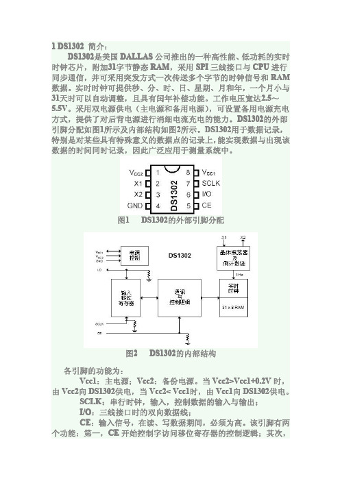
图6
控制字(即地址及命令字节)
控制字的最高有效位(位7)必须是逻辑1,如果它为0,则不能把 数据写入到 DS1302中。 位6:如果为0,则表示存取日历时钟数据,为1表示存取 RAM 数 据; 位5至位1(A4~A0) :指示操作单元的地址; 位0(最低有效位) :如为0,表示要进行写操作,为1表示进行读 操作。 控制字总是从最低位开始输出。在控制字指令输入后的下一个 SCLK 时钟的上升沿时,数据被写入 DS1302,数据输入从最低位(0 位)开始。同样,在紧跟8位的控制字指令后的下一个 SCLK 脉冲的 下降沿,读出 DS1302的数据,读出的数据也是从最低位到最高位。 数据读写时序如图7 。
图4 ③ DS1302的工作模式寄存器 所谓突发模式是指一次传送多个字节的时钟信号和 RAM 数据。 突发模式寄存器如图5所示。
图5 ④此外,DS1302还有充电寄存器等。 2 读写时序说明 DS1302是 SPI 总线驱动方式。它不仅要向寄存器写入控制字, 还需要读取相应寄存器的数据。 要想与 DS1302通信, 首先要先了解 DS1302的控制字。 DS1302 的控制字如图6。
//禁止写保 //秒位初始 //分钟初始化 // //
//发送数据 for ( i=8; i>0; i-- ) { SCLK = 0; temp = dat; DIO = (bit)(temp&0x01); dat >>= 1; SCLK = 1; } CE = 0; } //数据读取子程序 unsigned char Read1302 ( unsigned char addr ) { unsigned char i,temp,dat1,dat2; CE=0; SCLK=0; CE = 1; //发送地址 for ( i=8; i>0; i-- ) { SCLK = 0; temp = addr; DIO = (bit)(temp&0x01); 节 addr >>= 1; 一位 SCLK = 1; } //读取数据 for ( i=8; i>0; i-- ) { ACC_7=DIO; SCLK = 1; ACC>>=1; SCLK = 0; } CE=0; dat1=ACC; dat2=dat1/16; dat1=dat1%16;
DS1302中文资料
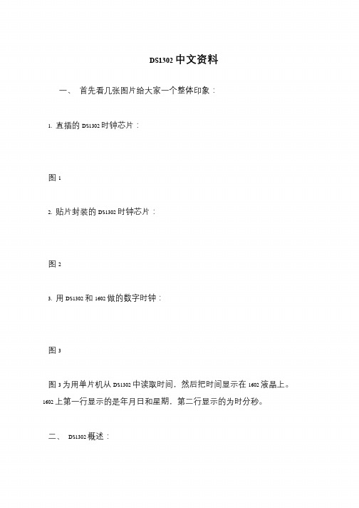
1.开发板电路图:
图4开发板电路图
从电路图中我们可以看到,RST片选使能引脚接到了单片机的P3.0引脚,
SCLK时钟引脚接到而来单片机的P3.3引脚,IO引脚接到了单片机的P2.4
引脚。
2.时序与数据读写:
对于操作一个芯片而言,最重要的应该是如何根据它的时序图向它里面写
入数据和读取数据。时序就是高低电平随时间的变化,和我们见到的波形随
DS1302中文资料
一、首先看几张图片给大家一个整体印象:
1.直插的DS1302时钟芯片:
图1
2.贴片封装的DS1302时钟芯片:
图2
3.用DS1302和1602做的数字时钟:
图3
图3为用单片机从DS1302中读取时间,然后把时间显示在1602液晶上。
1602上第一行显示的是年月日和星期,第二行显示的为时分秒。
时间变化差不多。下面教大家如何往芯片里面写数据,如何从芯片里面读数
据。温馨提示:在读写芯片时,一般需要先写入寄存器或RAM的地址(有时
也成为写入命令),然后才能对芯片的寄存器或RAM进行读写操作!
2.1往芯片里写数据:
因为芯片只识别0和1,所以写数据无非就是往芯片里面写0和1。那芯片
又是如何识别0和1的呢?其实我们只要在特定的时间把控制线置为高电平或
写操作的代码:
//地址、数据发送子程序
voidWrite1302(ucharaddr,dat)
{
uchari,temp,m,n;
RST=0;//RST引脚为低,数据传送中止
SCLK=0;//清零时钟总线
RST=1;//RST引脚为高,逻辑控制有效
//发送地址
for(i=8;i>0;i--)//循环8次移位
DS1302中文翻译译文
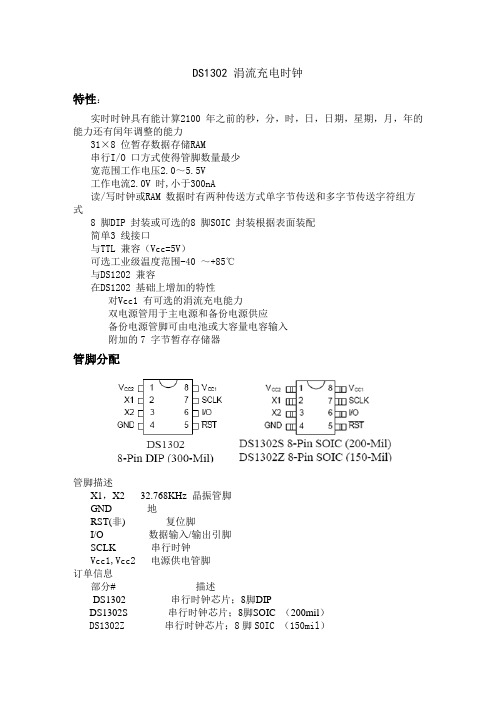
DS1302 涓流充电时钟特性:实时时钟具有能计算2100 年之前的秒,分,时,日,日期,星期,月,年的能力还有闰年调整的能力31×8 位暂存数据存储RAM串行I/O 口方式使得管脚数量最少宽范围工作电压2.0~5.5V工作电流2.0V 时,小于300nA读/写时钟或RAM 数据时有两种传送方式单字节传送和多字节传送字符组方式8 脚DIP 封装或可选的8 脚SOIC 封装根据表面装配简单3 线接口与TTL 兼容(Vcc=5V)可选工业级温度范围-40 ~+85℃与DS1202 兼容在DS1202 基础上增加的特性对Vcc1 有可选的涓流充电能力双电源管用于主电源和备份电源供应备份电源管脚可由电池或大容量电容输入附加的7 字节暂存存储器管脚分配管脚描述X1,X2 32.768KHz 晶振管脚GND 地RST(非) 复位脚I/O 数据输入/输出引脚SCLK 串行时钟Vcc1,Vcc2 电源供电管脚订单信息部分# 描述DS1302 串行时钟芯片;8脚DIPDS1302S 串行时钟芯片;8脚SOIC (200mil)DS1302Z 串行时钟芯片;8脚SOIC (150mil)概述DS1302 是DALLAS 公司推出的涓流充电时钟芯片,内含有一个实时时钟/日历和31 字节静态RAM,通过简单的串行接口与单片机进行通信。
实时时钟/日历电路提供秒、分、时、日、日期、月、年的信息,每月的天数和闰年的天数可自动调整,时钟操作可通过AM/PM 指示决定采用24 或12 小时格式。
DS1302 与单片机之间能简单地采用同步串行的方式进行通信,仅需用到三个口线:(1)RES (复位),(2)I/O(数据线),(3)SCLK(串行时钟)。
时钟/RAM 的读/写数据以一个字节或多达31 个字节的字符组方式通信。
DS1302 工作时功耗很低,保持数据和时钟信息时功率小于1mW。
DS1302是由DS1202改进而来,增加了以下的特性:双电源管脚用于主电源和备份电源供应,Vcc1 为可编程涓流充电电源,附加七个字节存储器。
ds1302中文资料
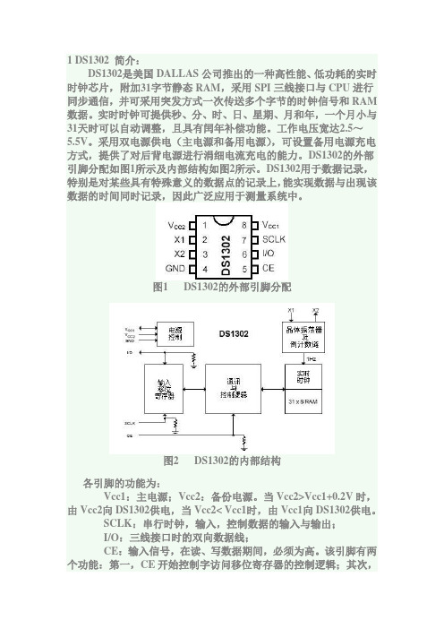
1 DS1302 简介:DS1302是美国DALLAS公司推出的一种高性能、低功耗的实时时钟芯片,附加31字节静态RAM,采用SPI三线接口与CPU进行同步通信,并可采用突发方式一次传送多个字节的时钟信号和RAM 数据。
实时时钟可提供秒、分、时、日、星期、月和年,一个月小与31天时可以自动调整,且具有闰年补偿功能。
工作电压宽达2.5~5.5V。
采用双电源供电(主电源和备用电源),可设置备用电源充电方式,提供了对后背电源进行涓细电流充电的能力。
DS1302的外部引脚分配如图1所示及内部结构如图2所示。
DS1302用于数据记录,特别是对某些具有特殊意义的数据点的记录上,能实现数据与出现该数据的时间同时记录,因此广泛应用于测量系统中。
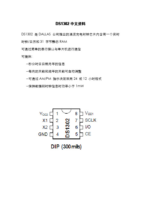
图1 DS1302的外部引脚分配图2 DS1302的内部结构各引脚的功能为:Vcc1:主电源;Vcc2:备份电源。
当Vcc2>Vcc1+0.2V时,由Vcc2向DS1302供电,当Vcc2< Vcc1时,由Vcc1向DS1302供电。
SCLK:串行时钟,输入,控制数据的输入与输出;I/O:三线接口时的双向数据线;CE:输入信号,在读、写数据期间,必须为高。
该引脚有两个功能:第一,CE开始控制字访问移位寄存器的控制逻辑;其次,CE提供结束单字节或多字节数据传输的方法。
DS1302有下列几组寄存器:① DS1302有关日历、时间的寄存器共有12个,其中有7个寄存器(读时81h~8Dh,写时80h~8Ch),存放的数据格式为BCD码形式,如图3所示。
图 3 DS1302有关日历、时间的寄存器小时寄存器(85h、84h)的位7用于定义DS1302是运行于12小时模式还是24小时模式。
当为高时,选择12小时模式。
在12小时模式时,位5是,当为1时,表示PM。
在24小时模式时,位5是第二个10小时位。
秒寄存器(81h、80h)的位7定义为时钟暂停标志(CH)。
当该位置为1时,时钟振荡器停止,DS1302处于低功耗状态;当该位置为0时,时钟开始运行。
DS1302是Dallas公司生产的一种实时时钟芯片
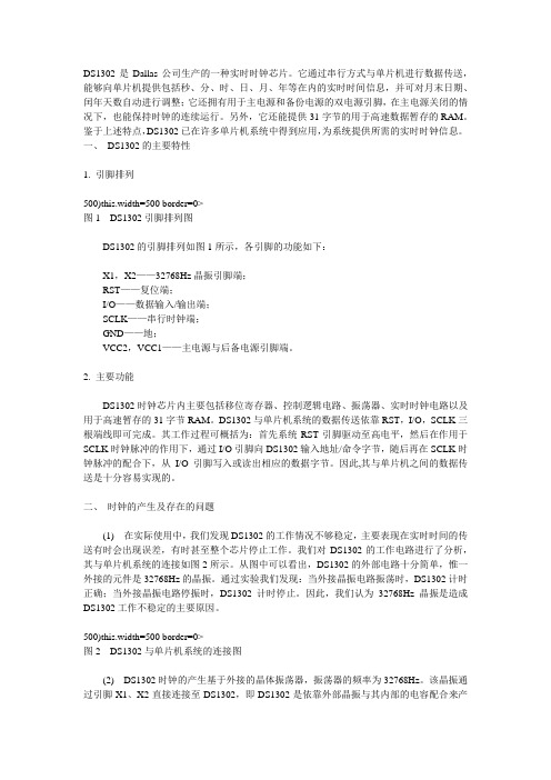
DS1302是Dallas公司生产的一种实时时钟芯片。
它通过串行方式与单片机进行数据传送,能够向单片机提供包括秒、分、时、日、月、年等在内的实时时间信息,并可对月末日期、闰年天数自动进行调整;它还拥有用于主电源和备份电源的双电源引脚,在主电源关闭的情况下,也能保持时钟的连续运行。
另外,它还能提供31字节的用于高速数据暂存的RAM。
鉴于上述特点,DS1302已在许多单片机系统中得到应用,为系统提供所需的实时时钟信息。
一、DS1302的主要特性1. 引脚排列500)this.width=500 border=0>图1 DS1302引脚排列图DS1302的引脚排列如图1所示,各引脚的功能如下:X1,X2——32768Hz晶振引脚端;RST——复位端;I/O——数据输入/输出端;SCLK——串行时钟端;GND——地;VCC2,VCC1——主电源与后备电源引脚端。
2. 主要功能DS1302时钟芯片内主要包括移位寄存器、控制逻辑电路、振荡器、实时时钟电路以及用于高速暂存的31字节RAM。
DS1302与单片机系统的数据传送依靠RST,I/O,SCLK三根端线即可完成。
其工作过程可概括为:首先系统RST引脚驱动至高电平,然后在作用于SCLK时钟脉冲的作用下,通过I/O引脚向DS1302输入地址/命令字节,随后再在SCLK时钟脉冲的配合下,从I/O引脚写入或读出相应的数据字节。
因此,其与单片机之间的数据传送是十分容易实现的。
二、时钟的产生及存在的问题(1) 在实际使用中,我们发现DS1302的工作情况不够稳定,主要表现在实时时间的传送有时会出现误差,有时甚至整个芯片停止工作。
我们对DS1302的工作电路进行了分析,其与单片机系统的连接如图2所示。
从图中可以看出,DS1302的外部电路十分简单,惟一外接的元件是32768Hz的晶振。
通过实验我们发现:当外接晶振电路振荡时,DS1302计时正确;当外接晶振电路停振时,DS1302计时停止。
ds1302中文资料
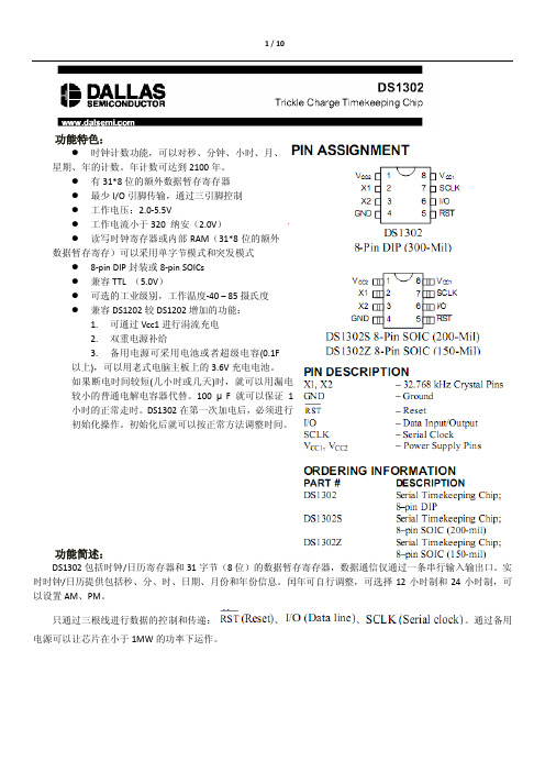
功能特色:●时钟计数功能,可以对秒、分钟、小时、月、星期、年的计数。
年计数可达到2100年。
●有31*8位的额外数据暂存寄存器●最少I/O引脚传输,通过三引脚控制●工作电压:2.0-5.5V●工作电流小于320 纳安(2.0V)●读写时钟寄存器或内部RAM(31*8位的额外数据暂存寄存)可以采用单字节模式和突发模式●8-pin DIP封装或8-pin SOICs●兼容TTL (5.0V)●可选的工业级别,工作温度-40 – 85摄氏度●兼容DS1202较DS1202增加的功能:1.可通过Vcc1进行涓流充电2.双重电源补给3.备用电源可采用电池或者超级电容(0.1F以上),可以用老式电脑主板上的3.6V充电电池。
如果断电时间较短(几小时或几天)时,就可以用漏电较小的普通电解电容器代替。
100 μF就可以保证1小时的正常走时。
DS1302在第一次加电后,必须进行初始化操作。
初始化后就可以按正常方法调整时间。
功能简述:DS1302包括时钟/日历寄存器和31字节(8位)的数据暂存寄存器,数据通信仅通过一条串行输入输出口。
实时时钟/日历提供包括秒、分、时、日期、月份和年份信息。
闰年可自行调整,可选择12小时制和24小时制,可以设置AM、PM。
只通过三根线进行数据的控制和传递:、、。
通过备用电源可以让芯片在小于1MW的功率下运作。
工作过程:主要工作原理图如Figure 1 所示:移位寄存器,控制逻辑,晶振,时钟和RAM 。
在进行任何数据传输时,必须被制高电平(注意虽然将它置为高电平,内部时钟还是在晶振作用下走时的,此时,允许外部读写数据),在每个SCLK 上升沿时数据被输入,下降沿时数据被输出,一次只能读写一位,适度还是写需要通过串行输入控制指令来实现(也是一个字节),通过8个脉冲便可读取一个字节从而实现串行输入与输出。
最初通过8个时钟周期载入控制字节到移位寄存器。
如果控制指令选择的是单字节模式,连续的8个时钟脉冲可以进行8位数据的写和8位数据的读操作,SCLK 时钟的上升沿时,数据被写入DS1302,SCLK 脉冲的下降沿读出DS1302的数据。
1 DS1302 简介
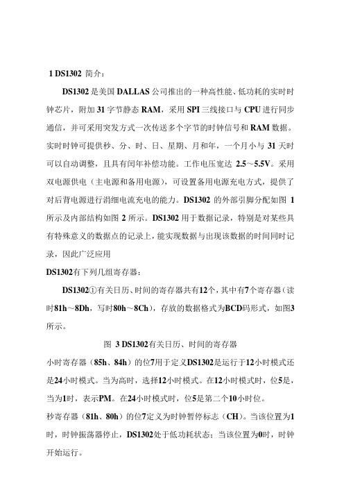
1 DS1302 简介:DS1302是美国DALLAS公司推出的一种高性能、低功耗的实时时钟芯片,附加31字节静态RAM,采用SPI三线接口与CPU进行同步通信,并可采用突发方式一次传送多个字节的时钟信号和RAM数据。
实时时钟可提供秒、分、时、日、星期、月和年,一个月小与31天时可以自动调整,且具有闰年补偿功能。
工作电压宽达2.5~5.5V。
采用双电源供电(主电源和备用电源),可设置备用电源充电方式,提供了对后背电源进行涓细电流充电的能力。
DS1302的外部引脚分配如图1所示及内部结构如图2所示。
DS1302用于数据记录,特别是对某些具有特殊意义的数据点的记录上,能实现数据与出现该数据的时间同时记录,因此广泛应用DS1302有下列几组寄存器:DS1302①有关日历、时间的寄存器共有12个,其中有7个寄存器(读时81h~8Dh,写时80h~8Ch),存放的数据格式为BCD码形式,如图3所示。
图3 DS1302有关日历、时间的寄存器小时寄存器(85h、84h)的位7用于定义DS1302是运行于12小时模式还是24小时模式。
当为高时,选择12小时模式。
在12小时模式时,位5是,当为1时,表示PM。
在24小时模式时,位5是第二个10小时位。
秒寄存器(81h、80h)的位7定义为时钟暂停标志(CH)。
当该位置为1时,时钟振荡器停止,DS1302处于低功耗状态;当该位置为0时,时钟开始运行。
控制寄存器(8Fh、8Eh)的位7是写保护位(WP),其它7位均置为0。
在任何的对时钟和RAM的写操作之前,WP位必须为0。
当WP位为1时,写保护位防止对任一寄存器的写操作。
DS1302②有关RAM的地址DS1302中附加31字节静态RAM的地址如图4所示。
图4DS1302③的工作模式寄存器所谓突发模式是指一次传送多个字节的时钟信号和RAM数据。
突发模式寄存器如图5所示。
图5④此外,DS1302还有充电寄存器等。
2 读写时序说明DS1302是SPI总线驱动方式。
DS 中文资料 带源代码

DS1302中文资料DS1302是DALLAS公司推出的涓流充电时钟芯片内含有一个实时时钟/日历和31字节静态RAM可通过简单的串行接口与单片机进行通信可提供:--秒分时日日期月年的信息--每月的天数和闰年的天数可自动调整--可通过AM/PM指示决定采用24或12小时格式--保持数据和时钟信息时功率小于1mWDS1302引脚X1X232.768KHz晶振管脚GND地CE复位脚I/O数据输入/输出引脚SCLK串行时钟Vcc1,Vcc2电源供电管脚各引脚的功能为:Vcc1:主电源;Vcc2:备份电源。
当Vcc2>Vcc1+0.2V时,由Vcc2向DS1302供电,当Vcc2<Vcc1时,由Vcc1向DS1302供电。
SCLK:串行时钟,输入,控制数据的输入与输出;I/O:三线接口时的双向数据线;CE:输入信号,在读、写数据期间,必须为高。
该引脚有两个功能:第一,CE开始控制字访问移位寄存器的控制逻辑;其次,CE提供结束单字节或多字节数据传输的方法。
参考电路:如上图所示:DS1302与单片机的连接也仅需要3条线:CE引脚、SCLK串行时钟引脚、I/O串行数据引脚,Vcc2为备用电源,外接32.768kHz晶振,为芯片提供计时脉冲。
实际电路:Vcc Vcc_5V _5V _5V::为电路中的为电路中的主电源;主电源;主电源;Vcc2Vcc2Vcc2,也就是,也就是BT1为备份电源。
当Vcc2>Vcc1+0.2V 时,由Vcc2向DS1302供电,当Vcc2<Vcc1时,由Vcc1向DS1302供电CLK 和I/O 虽然和IIC 总线接在一条引脚上总线接在一条引脚上,,但DS1302其实并不是使用IIC 总线,而是一种三线式总线,DS1302内部结构:DS1302内部包括:Power control:电源控制模块Input shift registers:输入移位寄存器Command and control logic:通讯与逻辑控制器Oscillator and divider:晶体振荡器及分频器DS1302的内部主要组成部分虽然有:移位寄存器、控制逻辑、振荡器、实时时钟以及RAM。
DS1302中文手册
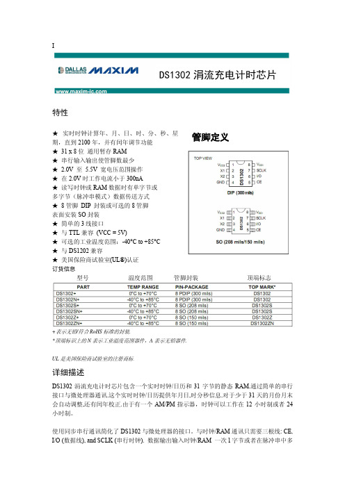
I特性★ 实时时钟计算年、月、日、时、分、秒、星期,直到2100年,并有闰年调节功能★ 31 x 8位 通用暂存RAM ★ 串行输入输出使管脚数最少 ★ 2.0V 至 5.5V 宽电压范围操作 ★ 在2.0V 时工作电流小于300nA★ 读写时钟或RAM 数据时有单字节或 多字节(脉冲串模式)数据传送方式 ★ 8管脚 DIP 封装或可选的8管脚 表面安装SO 封装 ★ 简单的3线接口★ 与TTL 兼容 (VCC = 5V)★ 可选的工业温度范围:-40°C to +85°C ★ 与DS1202兼容★ 美国保险商试验室(UL®)认证 订货信息型号 温度范围 管脚封装 顶端标志+表示无铅/符合RoHS 标准的封装.*顶端标识上的N 表示工业温度范围器件,A 表示无铅器件.UL 是美国保险商试验室的注册商标.详细描述DS1302涓流充电计时芯片包含一个实时时钟/日历和31字节的静态RAM.通过简单的串行接口与微处理器通讯.这个实时时钟/日历提供年月日,时分秒信息.对于少于31天的月份月末会自动调整,还有闰年校正.由于有一个AM/PM 指示器,时钟可以工作在12小时制或者24小时制。
使用同步串行通讯简化了DS1302与微处理器的接口。
与时钟/RAM 通讯只需要三根线: CE, I/O (数据线), and SCLK (串行时钟). 数据输出输入时钟/RAM 一次1字节或者在脉冲串中多管脚定义 D S 1302涓流充电计时芯片达31字节. DS1302被设计工作在非常低的电能下,在低于1μW 时还能保持数据和时钟信息. DS1302是DS1202的后继者. 除了DS1202的基本计时功能以外, DS1302有额外特点比如,双管脚主电源和备用电源,可编程涓流充电器V CC1,还附加7字节的暂存器.操作图1显示了串行计时器的主要元素:移位寄存器,控制逻辑,振荡器,实时时钟,还有RAM.典型工作电路图1 框图:典型工作性能(V C C = 3.3V , T A = +25°C ,除非另外声明.)电源控制输入 移位 寄存器命令控制逻辑实时时钟管脚描述管脚 名称 功能1V CC2双供电配置中的主电源供应管脚,V CC1连接到备用电源,在主电源失效时保持时间和日期数据.D S1302工作于V CC1和V CC2中较大者.当V CC2比V CC1高0.2V时,V CC2 给 D S1302供电.当V CC1比V CC2高时, V CC1给D S1302供电.2X1 3X2与标准的32.768k H z石英晶体相连.内部振荡器被设计与指定的6p F 装载电容的晶体一起工作.更多关于晶体选择和布局注意事项的信息请参考应用笔记58页:D a l l a s实时时钟晶振注意事项.D S1302也可以被外部的32.768k H z振荡器驱动.这种配置下,X1与外部震荡信号连接,X2悬浮.4G N D电源地5C E输入.C E信号在读写时必须保持高电平.此管脚内部有一个40kΩ(典型值)的下拉电阻连接到地.注意:先前的数据手册修正把C E当作R S T.管脚的功能没有改变.6I/O输入/推挽输出.I/O管脚是三线接口的双向数据管脚.此管脚内部有一个40kΩ(典型值)的下拉电阻连接到地.7S C L K输入.S C L K用来同步串行接口上的数据动作.此管脚内部有一个40kΩ(典型值)的下拉电阻连接到地.8V CC1低功率工作在单电源和电池工作系统和低功率备用电池.在使用涓流充电的系统中,这个管脚连接到可再充能量源.U L认证在使用锂电池时确保避免反向充电电流.详见w w w.m a x i m i c.c o m/T e c h S u p p o r t/Q A/n t r l.h t m.振荡电路D S1302使用一个外部32.768k H z晶体.振荡电路工作时不需要任何外接的电阻或者电容表1 详细指明了几个外部晶体的参数.图1 显示了震荡电路的功能简图.如果使用指定规格的晶体,启动时间通常少于1秒钟.时钟精确度时钟的精确度取决于晶振的精确度,以及振荡电路容性负载与晶振校正的容性负载之间匹配的精确度。
DS1302中文资料,带源代码
DS1302 引脚
X1 X2 32.768KHz 晶振管脚 GND 地 CE 复位脚 I/O 数据输入/输出引脚 SCLK 串行时钟 Vcc1,Vcc2 电源供电管脚
各引脚的功能为:
Vcc1:主电源;Vcc2:备份电源。当Vcc2>Vcc1+0.2V时,由Vcc2 向DS1302供电,当Vcc2< Vcc1时,由Vcc1向DS1302供电。 SCLK:串行时钟,输入,控制数据的输入与输出; I/O:三线接口时的双向数据线; CE:输入信号,在读、写数据期间,必须为高。该引脚有两个功能: 第一,CE开始控制字访问移位寄存器的控制逻辑;其次, CE 提供结束单字节或多字节数据传输的方法。
参考电路:
如上图所示: DS1302 与单片机的连接也仅需要 3 条线:CE 引脚、SCLK 串行时钟 引脚、I/O 串行数据引脚,Vcc2 为备用电源,外接 32.768kHz 晶振, 为芯片提供计时脉冲。
实际电路:
Vcc_5V:为电路中的主电源;Vcc2,也就是 BT1 为备份电源。当 Vcc2>Vcc1+0.2V 时, 由 Vcc2 向 DS1302 供 电 , 当 Vcc2< Vcc1 时 , 由 Vcc1 向 DS1302 供电 CLK 和 I/O 虽然和 IIC 总线接在一条引脚上,但 DS1302 其实并不是 使用 IIC 总线,而是一种三线式总线,
delayus(2); } return dat;//返回读取出的数据 }
寄存器和 RAM
对 DS1302 的操作就是对其内部寄存器的操作,DS1302 内部共有 12 个寄存器, 其中有: 7 个寄存器与日历、时钟相关,存放的数据位为 BCD 码形式。 此外,DS1302 还有年份寄存器、控制寄存器、充电寄存器、时钟突发寄存器 及与 RAM 相关的寄存器等。 时钟突发寄存器可一次性顺序读写除充电寄存器以外的寄存器。 如下所示:
DS1302中文资料_数据手册_参数
DS1302涓流充电计时芯片 6 13 CE和时钟控制驱动CE输入高电平会启动所有数据传输. CE输入有两个功能.首先,CE打开控制逻辑允 许访问地址/命令序列的移位寄存器.其次,CE信号提供了一种终止单字节或多字节CE数据传输的方法.时钟周期是一系列的上升沿, 然后是下降沿. DS1302对于数据输入,数据在过程中必须有效时钟的上升沿和数据位在时钟的下降沿输出.如果CE输入低,所有数据 传输终止,I / O引脚进入高阻状态.图4显示了数据传输.在通电时,CE 在V CC > 2.0V 之前必须为逻辑0 . 而且,当CE被驱动到逻 辑1状态时,SCLK必须处于逻辑0.数据输入在输入写命令字节的8个SCLK周期之后,数据字节在下一个的上升沿输入八个SCLK周期. 如果DS1302无意中出现其他SCLK周期,则会被忽略.数据以输入开始位0.数据输出在输入一个读命令字节的八个SCLK周期后,一个 数据字节在该输出的下降沿输出接下来的八个SCLK周期.请注意,要传输的个数据位发生在后一位之后的个下降沿的命令字节被写 入.额外的SCLK周期会在无意中发生数据字节时重新传输只要CE仍然很高.该操作允许连续突发模式读取能力.另外,I / O引脚是三态 的,在SCLK的每个上升沿发表.数据从位0开始输出.突发模式通过寻址31位十进制数可以为时钟/日历或RAM寄存器指定突发模式 (地址/命令位1至5 =逻辑1). DS1302如前所述,位6指定时钟或RAM,位0指定读取或写.时钟/日历寄存器中的位置9到31或位置31中 没有数据存储容量 RAM寄存器.在突发模式下读取或写入个寄存器,以便数据到达被转移.但是,在突发模式下写入RAM时,不需要为数据写入全部31个字节转让.无论是否写入全部31个 字节,写入的每个字节都将传输到RAM.时钟/日历时间和日历信息是通过读取适当的寄存器字节获得的.表3说明了RTC寄存 DS1302有主电源的情况下维护时间和日期.该 DS1302采用V CC1 或V CC2中 的较大者工作 . 当V CC2 大于V CC1 +时 0.2V,V CC2 为 DS1302供电. 当V CC2 小于V CC1时 ,V CC1 为 DS1302. 2 X1 3 X2标准32.768KHZ石英晶体的连接.内部振荡器是设计用于使用具有6PF 的指定负载电容的晶体进行操作.有关晶体选择和晶体布局注意事项的更多信息,请参阅应用笔记58:达拉斯实时时钟的晶体注意事 项 .该 DS1302也可以由外部32.768KHZ振荡器驱动.在这配置,X1引脚连接到外部振荡器信号和X2引脚漂浮. 4 GND地面五 CE输入.在 读取或写入期间,CE信号必须置为高电平.这个针有一个内部40K Ω(典型值)下拉电阻接地.注意:以前的数据表修订简称CE RST. 引脚的功能没有改变. 6 I / O输入/推挽输出. I / O引脚是3线的双向数据引脚接口.该引脚有一个内部40K Ω(典型值)下拉电阻接地. 7 SCLK输入. SCLK用于同步串行接口上??的数据移动.这个引脚有一个内部40K Ω(典型值)下拉电阻接地. 8 V CC1单电源和电池供电 系统中的低功耗操作以及低功耗,电池备份.在使用涓流充电器的系统中,可充电电池能源连接到此引脚. UL认可,以确保逆向充电 电流与锂电池一起使用
时钟芯片DS1302及其应用35页PPT

2、要冒一次险!整个生命就是一场冒险。走得最远的人,常是愿意 去做,并愿意去冒险的人。“稳妥”之船,从未能从岸边走远。-戴尔.卡耐基。
梦 境
3、人生就像一杯没有加糖的咖啡,喝起来是苦涩的,回味起来却有 久久不会退去的余香。
时钟芯片DS1302及其应用 4、守业的最好办法就是不断的发展。 5、当爱不能完美,我宁愿选择无悔,不管来生多么美丽,我不愿失 去今生对你的记忆,我不求天长地久的美景,我只要生生世世的轮 回里有你。
55、 为 中 华
51、 天 下 之 事 常成 于困约 ,而败 于奢靡 。——陆 游 52、 生 命 不 等 于是呼 吸,生 命是活 动。——卢 梭
53、 伟 大 的 事 业,需 要决心 ,能力 ,组织 和责任 感。 ——易 卜 生 54、 唯 书 籍 不 朽。——乔 特
- 1、下载文档前请自行甄别文档内容的完整性,平台不提供额外的编辑、内容补充、找答案等附加服务。
- 2、"仅部分预览"的文档,不可在线预览部分如存在完整性等问题,可反馈申请退款(可完整预览的文档不适用该条件!)。
- 3、如文档侵犯您的权益,请联系客服反馈,我们会尽快为您处理(人工客服工作时间:9:00-18:30)。
命令位
第七位必须为1,第6位(0为时钟和日历,1为RAM),第0位读/写读为1,写为0.
RST和时间控制
所有有效数据的传输都必须讲RST置高,第一,RST的打开允许了寄存器数据的传输;第二,RST提供了单字节传输和多字节传输。
一个时钟走起是由一个连续的上升沿和下降沿组成的,对于数据的输入,数据必须在时钟的上升沿才有校,对于数据的输出,数据必须在下降沿。
如果RST输入低,则所有数据输入结束,并且I/O口出去高阻抗状态。
数据的交换如图三。
在电压升高阶段,RST必须置
0知道VCC>2V,,并且s当rst置1时,clk必须置0。
BURST 模式
BURST模式是对于时钟/日历或者是RAM寄存器内部地址的规定。
之前第6为规定了时钟和RAM,而0位规定了读或者写。
在时钟和日历的寄存器还有RAM的寄存器上没有数据贮藏。
在BURST模式下读或者写从第0位或者0地址开始
在BURST模式下,当要写进时钟寄存器时,头8个寄存器必须写确保数据的传输。
然而,当要写进RAM时不需要将31位写满。
每个字节都会被传输到RAM中不管31位有没有写满
CLOCK/CALENDER
时钟/日历如图所示包括了7个读写寄存器,包含了二进制编码的十进制数据。
CLOCK HALT FALG(时钟停止标志)
秒寄存器的第7位用来定义时钟的停止标志。
当这位为1时,时钟振荡器被停止,并且时钟进入低功率的待命模式。
当这位为0时,时钟将启动,开始的功耗不确定。
AM-PM/12-24MODE
小时寄存器的第七位用来定义12小时制和24小时制。
为高时,12小时制。
低为24小时制。
第五位为AM和PM位,高为PM,在24小时制,第五位为第二个10小时位(20-23hours)WRITE PROTECT BIT(写保护位)
控制寄存器的第七位为写保护位,读的时候前面7位被强制变为0。
在任何写操作之前,第7位本来为0.当其为高时,它将保证任何寄存器的写操作。
所以在尝试写到设备中时,WP 位必须清零
TRICKLE CHARGE REGISTER
该寄存器控制DS1302的涓流参数。
图5展示了其最基础的部分,STC位控制涓流的选择。
为了保证意外不发生,只有1010的方式能启动涓流。
其他的任何方式都不能启动。
DS1302随着涓流的停止功率升高。
DS位选择在VCC1和VCC2之间一个二极管还是2个二级管连接。
如果DS为01,一个二极管被选择。
如果DS为10,2个二极管被选择。
如果DS为00或者11,涓流关闭不依赖于TCS。
RS位选择VCC1和VCC2之间的寄存器。
如果RS为00,涓流停止不依赖于TCS
二极管和寄存器的选择由使用者根据电流的理想最大值决定。
最大电流的计算如下例子。
CLOCK/CALENDAR BURST MODE
CLOCK/CALENDER的命令指令规定BURST MODE的操作,在这个模式下,头8个CLOCK/CALENDER寄存器随着第0位而不断读或者写(图4)
当写CLOCK/CALENDER BURST MODE规定时如果写保护位置高,没有数据可以传输到8个CLOCK/CALENDER寄存器上(包括控制寄存器),在BURST MODE下,涓流不会获得CLOCK BURST开始读的时候,现在的时间被传送到第二个寄存器上。
当时间继续走时,该时间信息被从第二寄存器读走,忽略再度寄存器的的需呀防止在读的过程中主寄存器的更新。
电容的选取……(自己看~~)。
