LM311N_NL中文资料
LM311M中文资料

©2001 Fairchild Semiconductor CorporationRev. 1.0.1Features•Low input bias current : 250nA (Max)•Low input offset current : 50nA (Max)•Differential Input V oltage : ±30V•Power supply voltage : single 5.0V supply to ±15V .•Offset voltage null capability.•Strobe capability.DescriptionThe LM311 series is a monolithic, low input current voltage comparator. The device is also designed to operate from dual or single supply voltage.8-DIP8-SOP11Internal Block DiagramLM311Single ComparatorLM3112Schematic DiagramAbsolute Maximum RatingsParameterSymbol Value UnitTotal Supply VoltageV CC 36V Output to Negative Supply Voltage LM311V O - V EE 40V Ground to Negative voltage V EE -30V Differential Input Voltage V I(DIFF)30V Input VoltageV I ±15V Output Short Circuit Duration -10sec Power DissipationP D 500mW Operating Temperature Range T OPR 0 ~ +70°C Storage Temperature RangeT STG- 65 ~ +150°CLM3113Electrical Characteristics(V CC = 15V, T A = 25°C, unless otherwise specified)Notes :1.0 ≤ T A ≤ +70°C2.The response time specified is for a 100mV input step with 5mV over drive.ParameterSymbol ConditionsMin.Typ.Max.Unit Input Offset Voltage V IO R S ≤ 50K Ω- 1.07.5mV Note 1--10Input Offset Current I IO -650nA Note 1--70Input Bias Current I BIAS -100250nA Note 1--300 Voltage Gain G V -40200-V/mV Response Time T RESNote 2-200-nsSaturation Voltage V SAT I O =50mA, V I ≤ -10mV-0.75 1.5V V CC ≥ 4.5V, V EE =0VI O =8mA, V I ≤ -10mV, Note 1-0.230.4 Strobe “ON” Current I STR(ON)--3-mA Output Leakage Current I SINK I STR =3mA, V I ≥ 10mV V O =15V, V CC =±15V -0.250nA Input Voltage Range V I(R)Note 1-14.5to13.0-14.7to 13.8-V Positive Supply Current I CC -- 3.07.5mA Negative Supply Current I EE ---2.2-5.0mA Strobe CurrentI STR--3-mALM3114Typical Performance CharacteristicsFigure 1.Input Bias Current vs Temperature Figure 2.Input Offset Current vs TemperatureFigure 3.Offset Voltage vs Input ResistanceFigure 4.Input Bias Current vs Differential input voltageFigure mon Mode Limits vs TemperatureFigure 6.Output Voltage vsDifferential input voltageLM3115Typical Performance Characteristics (continued)Figure 7.Saturation voltage vs Current Figure 8.Supply Current vs TemperatureFigure 9.Leakage Current vs Temperature Figure 10.Supply Current vs Supply VoltageFigure 11.Current Saturation Voltage Figure 12.Output Limiting CharactersticsLM311Mechanical DimensionsPackage8-DIP6LM311 Mechanical Dimensions (Continued)Package8-SOP7LM3118Ordering InformationProduct NumberPackage Operating TemperatureLM311N 8-DIP 0 ~ +70°CLM311M8-SOPLM3119LM3116/1/01 0.0m 001Stock#DSxxxxxxxx2001 Fairchild Semiconductor CorporationLIFE SUPPORT POLICYFAIRCHILD’S PRODUCTS ARE NOT AUTHORIZED FOR USE AS CRITICAL COMPONENTS IN LIFE SUPPORT DEVICES OR SYSTEMS WITHOUT THE EXPRESS WRITTEN APPROVAL OF THE PRESIDENT OF FAIRCHILD SEMICONDUCTOR CORPORATION. As used herein:1.Life support devices or systems are devices or systemswhich, (a) are intended for surgical implant into the body, or (b) support or sustain life, and (c) whose failure to perform when properly used in accordance with instructions for use provided in the labeling, can bereasonably expected to result in a significant injury of the user.2. A critical component in any component of a life supportdevice or system whose failure to perform can bereasonably expected to cause the failure of the life support device or system, or to affect its safety or effectiveness.DISCLAIMERFAIRCHILD SEMICONDUCTOR RESERVES THE RIGHT TO MAKE CHANGES WITHOUT FURTHER NOTICE TO ANY PRODUCTS HEREIN TO IMPROVE RELIABILITY, FUNCTION OR DESIGN. FAIRCHILD DOES NOT ASSUME ANYLIABILITY ARISING OUT OF THE APPLICATION OR USE OF ANY PRODUCT OR CIRCUIT DESCRIBED HEREIN; NEITHER DOES IT CONVEY ANY LICENSE UNDER ITS PATENT RIGHTS, NOR THE RIGHTS OF OTHERS.。
LM318N中文资料

LM118/LM218/LM318 Operational Amplifiers General DescriptionThe LM118series are precision high speed operational am-plifiers designed for applications requiring wide bandwidth and high slew rate.They feature a factor of ten increase in speed over general purpose devices without sacrificing DC performance.The LM118series has internal unity gain frequency compen-sation.This considerably simplifies its application since no external components are necessary for operation.However, unlike most internally compensated amplifiers,external fre-quency compensation may be added for optimum perfor-mance.For inverting applications,feedforward compensa-tion will boost the slew rate to over150V/µs and almost double the bandwidth.Overcompensation can be used with the amplifier for greater stability when maximum bandwidth is not needed.Further,a single capacitor can be added to reduce the0.1%settling time to under1µs.The high speed and fast settling time of these op amps make them useful in A/D converters,oscillators,active filters,sample and hold circuits,or general purpose amplifiers. These devices are easy to apply and offer an order of magnitude better AC performance than industry standards such as the LM709.The LM218is identical to the LM118except that the LM218 has its performance specified over a−25˚C to+85˚C tem-perature range.The LM318is specified from0˚C to+70˚C. Featuresn15MHz small signal bandwidthn Guaranteed50V/µs slew raten Maximum bias current of250nAn Operates from supplies of±5V to±20Vn Internal frequency compensationn Input and output overload protectedn Pin compatible with general purpose op ampsFast Voltage Follower(Note1)00776613 Note1:Do not hard-wire as voltage follower(R1≥5kΩ)August2000LM118/LM218/LM318 Operational Amplifiers©2004National Semiconductor Corporation Absolute Maximum Ratings (Note 7)If Military/Aerospace specified devices are required,please contact the National Semiconductor Sales Office/Distributors for availability and specifications.Supply Voltage±20VPower Dissipation (Note 2)500mWDifferential Input Current (Note 3)±10mA Input Voltage (Note 4)±15VOutput Short-Circuit Duration ContinuousOperating Temperature Range LM118−55˚C to +125˚C LM218−25˚C to +85˚C LM3180˚C to +70˚C Storage Temperature Range−65˚C to +150˚CLead Temperature (Soldering,10sec.)Hermetic Package 300˚C Plastic Package 260˚CSoldering Information Dual-In-Line Package Soldering (10sec.)260˚C Small Outline Package Vapor Phase (60sec.)215˚C Infrared (15sec.)220˚C See AN-450“Surface Mounting Methods and Their Effect on Product Reliability”for other methods of soldering surface mount devices.ESD Tolerance (Note 8)2000VElectrical Characteristics (Note 5)ParameterConditionsLM118/LM218LM318UnitsMinTyp Max MinTyp Max Input Offset Voltage T A =25˚C 24410mV Input Offset Current T A =25˚C 65030200nA Input Bias Current T A =25˚C 120250150500nA Input Resistance T A =25˚C 130.53M ΩSupply CurrentT A =25˚C58510mA Large Signal Voltage Gain T A =25˚C,V S =±15V 5020025200V/mV V OUT =±10V,R L ≥2k ΩSlew RateT A =25˚C,V S =±15V,A V =150705070V/µs(Note 6)Small Signal Bandwidth T A =25˚C,V S =±15V1515MHz Input Offset Voltage 615mV Input Offset Current 100300nA Input Bias Current 500750nA Supply CurrentT A =125˚C4.57mA Large Signal Voltage Gain V S =±15V,V OUT =±10V 2520V/mVR L ≥2k ΩOutput Voltage Swing V S =±15V,R L =2k Ω±12±13±12±13V Input Voltage RangeV S =±15V±11.5±11.5V Common-Mode Rejection Ratio 8010070100dB Supply Voltage Rejection Ratio70806580dBNote 2:The maximum junction temperature of the LM118is 150˚C,the LM218is 110˚C,and the LM318is 110˚C.For operating at elevated temperatures,devices in the H08package must be derated based on a thermal resistance of 160˚C/W,junction to ambient,or 20˚C/W,junction to case.The thermal resistance of the dual-in-line package is 100˚C/W,junction to ambient.Note 3:The inputs are shunted with back-to-back diodes for overvoltage protection.Therefore,excessive current will flow if a differential input voltage in excess of 1V is applied between the inputs unless some limiting resistance is used.Note 4:For supply voltages less than ±15V,the absolute maximum input voltage is equal to the supply voltage.Note 5:These specifications apply for ±5V ≤V S ≤±20V and −55˚C ≤T A ≤+125˚C (LM118),−25˚C ≤T A ≤+85˚C (LM218),and 0˚C ≤T A ≤+70˚C (LM318).Also,power supplies must be bypassed with 0.1µF disc capacitors.Note 6:Slew rate is tested with V S =±15V.The LM118is in a unity-gain non-inverting configuration.V IN is stepped from −7.5V to +7.5V and vice versa.The slew rates between −5.0V and +5.0V and vice versa are tested and guaranteed to exceed 50V/µs.Note 7:Refer to RETS118X for LM118H and LM118J military specifications.Note 8:Human body model,1.5k Ωin series with 100pF.L M 118/L M 218/L M 318 2Typical Performance CharacteristicsLM118,LM218Input CurrentVoltage Gain0077662500776626Power Supply Rejection Input Noise Voltage0077662700776628Common Mode Rejection Supply Current0077662900776630LM118/LM218/LM3183Typical Performance CharacteristicsLM118,LM218(Continued)Closed Loop OutputImpedanceCurrent Limiting0077663100776632Input Current Unity Gain Bandwidth0077663300776634Voltage Follower Slew Rate Inverter Settling Time0077663500776636L M 118/L M 218/L M 318 4Typical Performance CharacteristicsLM118,LM218(Continued)Large Signal FrequencyResponseOpen Loop FrequencyResponse0077663700776638Voltage Follower PulseResponse Large Signal FrequencyResponse0077663900776640Open Loop FrequencyResponseInverter Pulse Response0077664100776642LM118/LM218/LM3185Typical Performance CharacteristicsLM318Input CurrentVoltage Gain0077664300776644Power Supply Rejection Input Noise Voltage0077664500776646Common Mode Rejection Supply Current0077664700776648L M 118/L M 218/L M 318 6Typical Performance CharacteristicsLM318(Continued)Closed Loop Output ImpedanceCurrent Limiting0077664900776650Input Current Unity Gain Bandwidth0077665100776652Voltage Follower Slew Rate Inverter Settling Time0077665300776654LM118/LM218/LM3187Typical Performance CharacteristicsLM318(Continued)Large Signal FrequencyResponseOpen Loop FrequencyResponse0077665500776656Voltage Follower PulseResponse Large Signal FrequencyResponse0077665700776658Open Loop FrequencyResponseInverter Pulse Response0077665900776660L M 118/L M 218/L M 318 8Auxiliary CircuitsFeedforward Compensation for Greater Inverting Slew Rate(Note 9)00776608*Balance circuit necessary for increased slew.Note 9:Slew rate typically 150V/µs.Compensation for Minimum Settling Time(Note 10)00776609Note 10:Slew and settling time to 0.1%for a 10V step change is 800ns.Offset Balancing00776610Isolating Large Capacitive Loads00776611Overcompensation00776612LM118/LM218/LM3189Typical ApplicationsFast Voltage Follower(Note 11)00776613Integrator or Slow Inverter00776614C F =Large (C F ≥50pF)*Do not hard-wire as integrator or slow inverter;insert a 10k-5pF network in series with the input,to prevent oscillation.Note 11:Do not hard-wire as voltage follower (R1≥5k Ω)Fast Summing Amplifier 00776615Differential Amplifier00776616L M 118/L M 218/L M 318 10Typical Applications(Continued)Fast Sample and Hold00776618D/A Converter Using Ladder Network00776619*Optional —Reduces settling time.LM118/LM218/LM31811Typical Applications(Continued)Four Quadrant Multiplier00776617∆Output zero.*“Y”zero +“X”zero ‡Full scale adjust.D/A Converter Using Binary Weighted Network00776620*Optional —Reduces settling time.L M 118/L M 218/L M 318 12Typical Applications(Continued)Fast Summing Amplifier with Low Input Current00776621Wein Bridge Sine Wave Oscillator00776622Instrumentation Amplifier00776623LM118/LM218/LM31813Schematic Diagram00776601L M 118/L M 218/L M 318 14Connection DiagramDual-In-Line Package00776624Top ViewOrder Number LM118J/883(Note13)See NS Package Number J14ADual-In-Line Package00776603Top ViewOrder Number LM118J-8/883(Note13),LM318M or LM318NSee NS Package Number J08A,M08A or N08BMetal Can Package(Note12)00776602Top ViewOrder Number LM118H,LM118H/883(Note13),LM218H or LM318HSee NS Package Number H08CNote12:Pin connections shown on schematic diagram and typical applica-tions are for TO-5package.Note13:Available per JM38510/10107.LM118/LM218/LM31815Physical Dimensionsinches (millimeters)unless otherwise notedMetal Can Package (H)Order Number LM118H,LM118H/883,LM218H or LM318HNS Package Number H08CCeramic Dual-In-Line Package (J)Order Number LM118J-8/883NS Package Number J08AL M 118/L M 218/L M 318 16Physical Dimensionsinches (millimeters)unless otherwise noted (Continued)Ceramic Dual-In-Line Package (J)Order Number LM118J/883NS Package Number J14AS.O.Package (M)Order Number LM318M or LM318MXNS Package Number M08ALM118/LM218/LM31817Physical Dimensionsinches (millimeters)unless otherwise noted (Continued)Molded Dual-In-Line Package (N)Order Number LM318N NS Package Number N08ELIFE SUPPORT POLICYNATIONAL’S PRODUCTS ARE NOT AUTHORIZED FOR USE AS CRITICAL COMPONENTS IN LIFE SUPPORT DEVICES OR SYSTEMS WITHOUT THE EXPRESS WRITTEN APPROVAL OF THE PRESIDENT AND GENERAL COUNSEL OF NATIONAL SEMICONDUCTOR CORPORATION.As used herein:1.Life support devices or systems are devices or systems which,(a)are intended for surgical implant into the body,or (b)support or sustain life,and whose failure to perform when properly used in accordance with instructions for use provided in the labeling,can be reasonably expected to result in a significant injury to the user. 2.A critical component is any component of a life support device or system whose failure to perform can be reasonably expected to cause the failure of the life support device or system,or to affect its safety or effectiveness.BANNED SUBSTANCE COMPLIANCENational Semiconductor certifies that the products and packing materials meet the provisions of the Customer Products Stewardship Specification (CSP-9-111C2)and the Banned Substances and Materials of Interest Specification (CSP-9-111S2)and contain no ‘‘Banned Substances’’as defined in CSP-9-111S2.National Semiconductor Americas Customer Support CenterEmail:new.feedback@ Tel:1-800-272-9959National SemiconductorEurope Customer Support CenterFax:+49(0)180-5308586Email:europe.support@Deutsch Tel:+49(0)6995086208English Tel:+44(0)8702402171Français Tel:+33(0)141918790National Semiconductor Asia Pacific Customer Support CenterEmail:ap.support@National SemiconductorJapan Customer Support Center Fax:81-3-5639-7507Email:jpn.feedback@ Tel:81-3-5639-7560L M 118/L M 218/L M 318O p e r a t i o n a l A m p l i f i e r sNational does not assume any responsibility for use of any circuitry described,no circuit patent licenses are implied and National reserves the right at any time without notice to change said circuitry and specifications.。
LM337T_NL中文资料

©2001 Fairchild Semiconductor CorporationRev. 1.0.0Features•Output current in excess of 1.5A•Output voltage adjustable between -1.2V and - 37V •Internal thermal overload protection •Internal short circuit current limiting •Output transistor safe area compensation•Floating operation for high voltage applications •Standard 3-pin TO-220 packageDescriptionThe LM337 is a 3-terminal negative adjustable regulator. It supplies in excess of 1.5A over an output voltage range of -1.2V to - 37V . This regulator requires only two external resistor to set the output voltage. Included on the chip are current limiting, thermal overload protection and safe area compensation.TO-2201. Adj2. Input3. Output1LM3373-Terminal 1.5A Negative Adjustable RegulatorLM3372Absolute Maximum RatingsElectrical Characteristics(V I - V O = 5V, I O = 40mA, 0°C ≤ T J ≤ +125°C, P DMAX = 20W, unless otherwise specified)Note:1. Load and line regulation are specified at constant junction temperature. Change in V O due to heating effects must be taken intoaccount separately. Pulse testing with low duty is used.2. C ADJ , when used, is connected detween the adjustment pin and ground.ParameterSymbol Value Unit Input-Output Voltage Differential |V I - V O |40V Power DissipationP D Internally limitedW Operating Temperature Range T OPR 0 ~ +125°C Storage Temperature RangeT STG-65 ~+125°CParameterSymbolConditionsMin Typ.Max.Unit Line Regulation (Note1)R line T A = +25°C3V ≤ I V I - V O I ≤ 40V -0.010.04%/ V3V ≤ I V I - V O I ≤ 40V -0.020.07Load Regulation (Note1)R loadT A = +25°C10mA ≤ I O ≤ 0.5A -1550mV10mA ≤ I O ≤ 1.5A-15150Adjustable Pin Current I ADJ --50100µA Adjustable Pin Current Change∆I ADJT A =+ 25°C10mA ≤ I O ≤ 1.5A 3V ≤I V I - V O I ≤ 40V -25µA T A =+ 25°C-1.213-1.250-1.287Reference Voltage V REF 3V ≤ I V I - V O I ≤ 40V 10mA ≤ I O ≤ 1.5A -1.200-1.250-1.300V Temperature StabilityST T 0°C ≤ ΤJ ≤ +125°C -0.6-%Minimum Load Current to Maintain Regulation I L(MIN)3V ≤I V I - V O I ≤ 40V - 2.5103V ≤I V I - V O I ≤ 10V - 1.56mA Output Noisee N T A =+25°C 10Hz ≤f ≤10KHz -0.003-V/106Ripple Rejection Ratio RR V O = -10V, f = 120Hz -60-C ADJ = 10µF (Note2)6677-dB Long Term StabilityST T J = 125°C ,1000Hours-0.31%Thermal Resistance Junction to CaseR θJC--4-°C/ WLM337 Typical ApplicationFigure 1.Programmable Regulator•Ci is required if regulator is located more then 4 inches from power supply filter.A 1.0µF solid tantalum or 10µF aluminum electrolytic is recommended.Co is necessary for stability. A 1.0µF solid tantalum or 10µF aluminum electrolytic is recommended.•V O= -1.25V (1+R2/R1)3LM3374Mechanical DimensionsPackage4.50 ±0.209.90 ±0.201.52 ±0.100.80 ±0.102.40 ±0.2010.00 ±0.201.27 ±0.10ø3.60 ±0.10(8.70)2.80 ±0.1015.90 ±0.2010.08 ±0.3018.95M A X .(1.70)(3.70)(3.00)(1.46)(1.00)(45°)9.20 ±0.2013.08 ±0.201.30 ±0.101.30+0.10–0.050.50+0.10–0.052.54TYP [2.54 ±0.20]2.54TYP [2.54 ±0.20]TO-220LM337 Ordering InformationProduct Number Package Operating TemperatureLM337T TO-2200°C to + 125°C5LM3376/1/01 0.0m 001Stock#DSxxxxxxxx2001 Fairchild Semiconductor CorporationLIFE SUPPORT POLICYFAIRCHILD’S PRODUCTS ARE NOT AUTHORIZED FOR USE AS CRITICAL COMPONENTS IN LIFE SUPPORT DEVICES OR SYSTEMS WITHOUT THE EXPRESS WRITTEN APPROVAL OF THE PRESIDENT OF FAIRCHILD SEMICONDUCTOR CORPORATION. As used herein:1.Life support devices or systems are devices or systemswhich, (a) are intended for surgical implant into the body, or (b) support or sustain life, and (c) whose failure to perform when properly used in accordance with instructions for use provided in the labeling, can bereasonably expected to result in a significant injury of the user.2. A critical component in any component of a life supportdevice or system whose failure to perform can bereasonably expected to cause the failure of the life support device or system, or to affect its safety or effectiveness.DISCLAIMERFAIRCHILD SEMICONDUCTOR RESERVES THE RIGHT TO MAKE CHANGES WITHOUT FURTHER NOTICE TO ANY PRODUCTS HEREIN TO IMPROVE RELIABILITY, FUNCTION OR DESIGN. FAIRCHILD DOES NOT ASSUME ANYLIABILITY ARISING OUT OF THE APPLICATION OR USE OF ANY PRODUCT OR CIRCUIT DESCRIBED HEREIN; NEITHER DOES IT CONVEY ANY LICENSE UNDER ITS PATENT RIGHTS, NOR THE RIGHTS OF OTHERS.。
LM211N中文资料

µA mA mA
NOTES: 1. This rating applies for ±15V supplies. The positive input voltage limit is 30V above the negative supply. The negative input voltage limit is equal to the negative supply voltage or 30V below the positive supply, whichever is less. 2. These specifications apply for VS=±15V and 0°C < TA < 70°C unless otherwise specified. With the LM211, however, all temperature specifications are limited to -25°C ≤ TA ≤ 85°C and for the LM111 is limited to -55°C TA < 125°C. The offset voltage, offset current, and bias current specifications apply for any supply voltage from a single 5V supply up to ±15V supplies. 3. The offset voltages and offset currents given are the maximum values required to drive the output within a volt of either supply with 1mA load. Thus, these parameters define an error band and take into account the worst case effects of voltage gain and input impedance. 4. The response time specified is for a 100mV input step with 5mV over-drive. 5. Do not short the strobe pin to ground; it should be current driven at 3mA to 5mA. 6. LM311B, all parameters are at V+ = 3V ±10%, V– = GND = 0V.
LM311电压比较器(含内部电路图,参数)
LM311 LM211中文资料时间:2009-08-06 20:01:15 来源:资料室作者:LM111/LM211/LM311电压比较器集成电路该LM111,LM211和LM311的电压比较器设计运行在更宽的电源电压:从标准的±15V运算放大器到单5V电源用于逻辑集成电路。
其输出兼容RTL,DTL和TTL以MOS电路。
此外,他们可以驱动继电器,开关电压高达50V,电流高达50mA。
LM111 LM211 绝对最大额定值:Total Supply Voltage (V84) 总供给电压(V84)36VOutput to Negative Supply Voltage (V74)输出到负电源电压(V74)50VGround to Negative Supply Voltage (V14)地到负电源电压(v14)30VDifferential Input Voltage 差分输入电压±30VInput Voltage (Note 4) 输入电压(注4)±15VOutput Short Circuit Duration 输出短路持续时间10秒10 secOperating Temperature Range 工作温度范围LM111−55℃ to 125℃LM211−25℃ to 85℃LM111 LM211 电气特性:P ar a m et er 参数Conditions测试条件Min最小Typ典型Max最大Units单位In p TA0.73.mVut Of fs et V ol ta g e 输入偏移电压(注7)= 2 5℃, R S ≤5 0 kIn p ut Of fset C ur re nt 输入失调电流TA=25℃4.1nAIn put Bi as C ur re nt 输TA=25℃61nA入偏置电流V ol tag e G ai n 电压增益TA=25℃42V/mVR es p o ns e Tim e ( N ot e 8) 响应时间(注8)TA=25℃2nsS at ur at io n VIN≤−5mV,0.751.5Vol ta g e 饱和电压O U T = 5 0 m A T A = 2 5℃St ro b eO N C ur re nt ( N ot e 9)TA=25℃2.5.mAO ut p ut Le a k a g e C ur re nt VIN≥5mV,VOUT=35V0.21nA出漏电流A = 2 5℃,I S T R O B E = 3 m AIn p ut Of fs et Vol ta g e 输入偏移电压(注7)RS≤5k4.mVIn put Of fs et C 2nAur re nt 输入失调电流(注7)In p ut Bi as Cur re nt 输入偏置电流15nAIn p ut V ol ta g e R a n g e 输入电压V+=15V,V−=−15V,Pin7P−14.513.8,-14.713.V。
LM311(单比较器)

MARKING DIAGRAMS
8 PDIP–8 N SUFFIX CASE 626 1 8 LMx11 ALYW LM311N AWL YYWW
+ –
Inputs
3
4 VEE Split Power Supply with Offset Balance
VCC 2 Inputs 3
2
LM211, LM311
8 5 6 1.3Ăk 300 300 3.7Ăk 1.3Ăk 100 3.7Ăk 300 250 900 600 2 Inputs 3 730 340 1.3Ăk 1.3Ăk 800 1 5.4Ăk 4 Gnd VEE 800 800 3.0Ăk 5.0Ăk 200 VCC
+ –
TTL Strobe 1.0Ăk
LM211D LM211DR2 LM311D LM311DR2 LM311N
Strobe Capability
Figure 1. Typical Comparator Design Configurations
© Semiconductor Components Industries, LLC, 2002
VCC 7 Output 2 Inputs 3
+ –
4 VEE
8 1
+ –
4
8 1
RL
PIN CONNECTIONS
Gnd Inputs VEE
1 2 3 4 8
Input polarity is reversed when Gnd pin is used as an output. Ground–Referty is reversed when Gnd pin is used as an output. Load Referred to Negative Supply
LM311中文资料_数据手册_参数

D Fast Response Times D Strobe Capability D Maximum Input Bias Current . . . 300 nA D Maximum Input Offset Current . . . 70 nA
LM311D LM311DR LM311PSR
LM311 L311
TSSOP (PW)
Reel of 150 Tube of 2000
LM311PW LM311PWR
L311
PDIP (P)
Tube of 50
LM211P
LM211P
–40°C to 85°C
3 mV
SOIC (D)
Tube of 75 Reel of 2500
SLCS007H – SEPTEMBER 1973 – REVISED AUGUST 2003
D Can Operate From Single 5-V Supply D Available in Q-Temp Automotive
– High-Reliability Automotive Applications – Configuration Control/Print Support – Qualification to Automotive Standards
LM111 . . . JG PACKAGE LM211 . . . D, P, OR PW PACKAGE LM311 . . . D, P, PS, OR PW PACKAGE
(TOP VIEW)
EMIT OUT 1 IN+ 2 IN– 3
LM310资料

闭的。
LM310 的实时测量值显示:
7.2.2. 事件记录 循环显示状态下,按下 SHIFT 键持续 3s 后进入事件记录,如无故障发生,则显示“没
有故障发生”或“No tr”,并返回循环显示。 故障查询时停留在最新一次故障原因与故障数据画面。按 MODE 键显示上一次故障原
因,总共可查询三次故障原因,查询完毕后按 RESET 键返回循环显示。
设定范围:
反时限堵转延时 tEp:1.0 – 15.0s
动作延时特性表: 见附表一
其中:
tEp 7 倍额定电流时允许堵转时间
IA
堵转电流
IN
电动机额定电流(即 Im 或 IL)
动作条件
保护投入
D7=1
当电流大于等于 2 倍额定电流时启动,按以上特性曲线动作。
容差
tEp 延时时间误差 ≤±10%
6.5. 零序过流保护
按顺序显示下一屏内容。再按一次 SHIFT 键又进入循环显示模式。 LM300 的实时测量值显示:
Ia= 176.5 A Ib= 176.0 A
Ic= 176.2 A Io= 0.0 A
电机累计运行时间
2368 小时
第一屏
第二屏
第三屏
注:LCD 背光只在循环显示模式下才关闭;在定点显示模式下,为了提示,背光是不关
— 自动计算零序电流,不需要外接零序互感器。
— 带独立的延时计时器。
设定范围
零序过流倍数 I0
0.5 – 8.0(Im)
延时时间 t0
0.1 – 5.0s
动作条件 保护投入 IE≥I0×Im t=t0 其中:
容差 启动值 延时时间
D3=1
IE
零序电流的实时测量值
NE531中文资料
0.4 300
0.4 400
2
2
RS≤10kΩ
Over temp RS≤10kΩ TA=25°C RL≥10kΩ, over temp TA=25°C TMAX TA=25°C RS≤10kΩ, TA=25°C
RL≥10kΩ, VOUT=±10V
AVOL VINN ISC Large-signal voltage gain Input noise voltage Short-circuit current RL≥10kΩ, VOUT=±10V, over temp 25°C f=1kHz 25°C
元器件交易网
Philips Semiconductors Linear Products Product specification
High slew rate operational amplifier
NE/SE531
DESCRIPTION
The 531 is a fast slewing high performance operational amplifier which retains DC performance equal to the best general purpose types while providing far superior large-signal AC performance. A unique input stage design allows the amplifier to have a large-signal response nearly identical to its small-signal response. The amplifier is compensated for truly negligible overshoot with a single capacitor. In applications where fast settling and superior large-signal bandwidths are required, the amplifier out-performs conventional designs which have much better small-signal response. Also, because the small-signal response is not extended, no special precautions need be taken with circuit board layout to achieve stability. The high gain, simple compensation, and excellent stability of this amplifier allow its use in a wide variety of instrumentation applications.
LM111N中文资料

• Precision squarer • Positive/negative peak detector • Low voltage adjustable reference supply • Switching power amplifier
TEMPERATURE RANGE -55°C to +125°C -25°C to +85°C 0 to +70°C 0 to +70°C -25°C to +85°C -55°C to +125°C 0 to +70°C 0 to +70°C
元器件交易网
Philips Semiconductors Linear Products Product specification
Voltage comparator
LM111/211/311/ LM311B
DESCRIPTION
The LM111 series are voltage comparators that have input currents approximately a hundred times lower than devices like the µA710. They are designed to operate over a wider range of supply voltages; from standard ±15V op amp supplies down to a single 3V supply. Their output is compatible with RTL, DTL, and TTL as well as MOS circuits. Further, they can drive lamps or relays, switching voltages up to 50V at currents as high as 50mA. Both the inputs and the outputs of the LM111 series can be isolated from system ground, and the output can drive loads referred to ground, the positive supply, or the negative supply. Offset balancing and strobe capability are provided and outputs can be wire-ORed. Although slower than the µA710 (200ns response time vs 40ns), the devices are also much less prone to spurious oscillations. The LM111 series has the same pin configuration as the µA710 series.
LM311N中文资料

Order this document by LM311/D
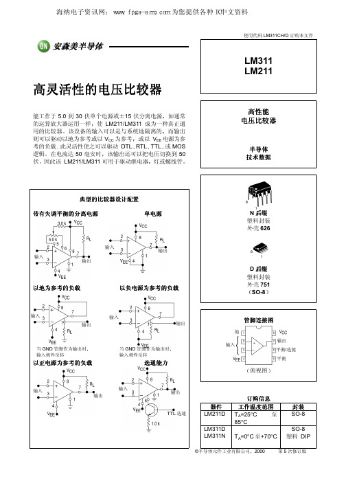
Highly Flexible Voltage Comparators
The ability to operate from a single power supply of 5.0 V to 30 V or ±15 V split supplies, as commonly used with operational amplifiers, makes the LM211/LM311 a truly versatile comparator. Moreover, the inputs of the device can be isolated from system ground while the output can drive loads referenced either to ground, the VCC or the VEE supply. This flexibility makes it possible to drive DTL, RTL, TTL, or MOS logic. The output can also switch voltages to 50 V at currents to 50 mA. Thus the LM211/LM311 can be used to drive relays, lamps or solenoids.
VCC Output Balance/Strobe Balance
VEE Input polarity is reversed when Gnd pin is used as an output.
Inputs
3
+ –
7 6 5
IRMCK311TR;中文规格书,Datasheet资料
Data Sheet No. PD60338IRMCK311 Dual Channel Sensorless Motor Control IC forAppliancesFeaturesMCE TM (Motion Control Engine) - Hardware based computation engine for high efficiency sinusoidal sensorless control of permanent magnet AC motor Integrated Power Factor Correction controlSupports both interior and surface permanent magnet motorsBuilt-in hardware peripheral for single shunt current feedback reconstructionNo external current or voltage sensing operational amplifier requiredDual channel three/two-phase Space Vector PWM Three-channel analog output (PWM)Embedded 8-bit high speed microcontroller (8051) for flexible I/O and man-machine controlJTAG programming port for emulation/debugger Two serial communication interface (UART)I2C/SPI serial interfaceWatchdog timer with independent analog clockThree general purpose timers/countersTwo special timers: periodic timer, capture timer Internal ‘One-Time Programmable’ (OTP) memory and internal RAM for final production usagePin compatible with IRMCF311 RAM version1.8V/3.3V CMOS Product SummaryMaximum crystal frequency 60 MHz Maximum internal clock (SYSCLK) frequency 128 MHz Maximum 8051 clock frequency 33 MHz Sensorless control computation time 11 μsec typ MCE TM computation data range 16 bit signed 8051 OTP Program memory 56K bytes MCE program and Data RAM 8K bytes GateKill latency (digital filtered) 2 μsec PWM carrier frequency counter 16 bits/ SYSCLK A/D input channels 6 A/D converter resolution 12 bits A/D converter conversion speed 2 μsec 8051 instruction execution speed 2 SYSCLK Analog output (PWM) resolution 8 bits UART baud rate (typ) 57.6K bps Number of I/O (max) 14 Package (lead-free) QFP64 Operating temperature -40°C ~ 85°CDescriptionIRMCK311 is a high performance OTP based motion control IC designed primarily for appliance applications. IRMCK311 is designed to achieve low cost and high performance control solutions for advanced inverterized appliance motor control. IRMCK311 contains two computation engines. One is Motion Control Engine (MCE TM) for sensorless control of permanent magnet motors; the other is an 8-bit high-speed microcontroller (8051). Both computation engines are integrated into one monolithic chip. The MCE TM contains a collection of control elements such as Proportional plus Integral, Vector rotator, Angle estimator, Multiply/Divide, Low loss SVPWM, Single Shunt IFB. The user can program a motion control algorithm by connecting these control elements using a graphic compiler. Key components of the sensorless control algorithms, such as the Angle Estimator, are provided as complete pre-defined control blocks implemented in hardware. A unique analog/digital circuit and algorithm to fully support single shunt current reconstruction is also provided. The 8051 microcontroller performs 2-cycle instruction execution (16MIPS at 33MHz). The MCE and 8051 microcontroller are connected via dual port RAM to process signal monitoring and command input. An advanced graphic compiler for the MCE TM is seamlessly integrated into the MATLAB/Simulink environment, while third party JTAG based emulator tools are supported for 8051 developments. IRMCK311 comes with a small QFP64 pin lead-free package.TABLE OF CONTENTS1 Overview (5)2 IRMCK311 Block Diagram and Main Functions (6)3 Pinout (8)4 Input/Output of IRMCK311 (9)4.1 8051 Peripheral Interface Group (10)4.2 Motion Peripheral Interface Group (10)4.3 Analog Interface Group (11)4.4 Power Interface Group (11)4.5 Test Interface (12)5 Application Connections (13)6 DC Characteristics (14)6.1 Absolute Maximum Ratings (14)6.2 System Clock Frequency and Power Consumption (14)6.3 Digital I/O DC Characteristics (15)6.4 PLL and Oscillator DC Characteristics (15)6.5 Analog I/O DC Characteristics (16)6.6 Under Voltage Lockout DC Characteristics (17)6.7 AREF Characteristics (17)7 AC Characteristics (18)7.1 PLL AC Characteristics (18)7.2 Analog to Digital Converter AC Characteristics (19)7.3 Op Amp AC Characteristics (19)7.4 SYNC to SVPWM and A/D Conversion AC Timing (20)7.5 GATEKILL to SVPWM AC Timing (21)7.6 Interrupt AC Timing (21)7.7 I2C AC Timing (22)7.8 SPI AC Timing (23)7.8.1 SPI Write AC timing (23)7.8.2 SPI Read AC Timing (24)7.9 UART AC Timing (25)7.10 CAPTURE Input AC Timing (26)7.11 JTAG AC Timing (27)7.12 OTP Programming Timing (28)8 I/O Structure (29)9 Pin List (32)Dimensions (35)10 Package11 Part Marking Information (36)Information (36)12 OrderingTABLE OF FIGURESFigure 1. Typical Application Block Diagram Using IRMCK311 (5)Figure 2. IRMCK311 Internal Block Diagram (6)Figure 3. IRMCK311 Pin Configuration (8)Figure 4. Input/Output of IRMCK311 (9)Figure 5. Application Connection of IRMCK311 (13)Figure 6. Clock Frequency vs. Power Consumption (14)Figure 7 Crystal oscillator circuit (18)Figure 8 Voltage droop of sample and hold (19)Figure 9 SYNC to SVPWM and A/D conversion AC Timing (20)Figure 10 GATEKILL to SVPWM AC Timing (21)Figure 11 Interrupt AC Timing (21)Figure 12 I2C AC Timing (22)Figure 13 SPI AC Timing (23)Figure 14 SPI Read AC Timing (24)Figure 15 UART AC Timing (25)Figure 16 CAPTURE Input AC Timing (26)Figure 17 JTAG AC Timing (27)Figure 18 OTP Programming Timing (28)Figure 19 All digital I/O except motor PWM output (29)Figure 20 RESET, GATEKILL I/O (29)Figure 21 Analog input (30)Figure 22 Analog operational amplifier output and AREF I/O structure (30)Figure 23 VPP programming pin I/O structure (30)Figure 24 VSS and AVSS pin structure (31)Figure 25 VDD1 and VDDCAP pin structure (31)Figure 26 XTAL0/XTAL1 pins structure (31)TABLE OF TABLESTable 1. Absolute Maximum Ratings (14)Table 2. System Clock Frequency (14)Table 3. Digital I/O DC Characteristics (15)Table 4. PLL DC Characteristics (15)Table 5. Analog I/O DC Characteristics (16)Table 6. UVcc DC Characteristics (17)Table 7. AREF DC Characteristics (17)Table 8. PLL AC Characteristics (18)Table 9. A/D Converter AC Characteristics (19)Table 10. Current Sensing OP Amp AC Characteristics (19)Table 11. SYNC AC Characteristics (20)Table 12. GATEKILL to SVPWM AC Timing (21)Table 13. Interrupt AC Timing (21)Table 14. I2C AC Timing (22)Table 15. SPI Write AC Timing (23)Table 16. SPI Read AC Timing (24)Table 17. UART AC Timing (25)Table 18. CAPTURE AC Timing (26)Table 19. JTAG AC Timing (27)Table 20. OTP Programming Timing (28)Table 21. Pin List (32)1 OverviewIRMCK311 is a new International Rectifier integrated circuit device primarily designed as a one-chip solution for complete inverter controlled appliance dual motor control applications. Unlike a traditional microcontroller or DSP, the IRMCK311 provides a built-in closed loop sensorless control algorithm using the unique Motion Control Engine (MCE TM) for permanent magnet motors. The MCE TM consists of a collection of control elements, motion peripherals, a dedicated motion control sequencer and dual port RAM to map internal signal nodes. IRMCK311 also employs a unique single shunt current reconstruction circuit to eliminate additional analog/digital circuitry and enables a direct shunt resistor interface to the IC. The sensorless control is the same for both motors with a single shunt current sensing capability. Motion control programming is achieved using a dedicated graphical compiler integrated into the MATLAB/Simulink TM development environment. Sequencing, user interface, host communication, and upper layer control tasks can be implemented in the 8051 high-speed 8-bit microcontroller. The 8051 microcontroller is equipped with a JTAG port to facilitate emulation and debugging tools. Figure 1 shows a typical application schematic using IRMCK311.IRMCK311 is intended for volume production purpose and contains 64K bytes of OTP (One Time Programming) ROM, which can be programmed through a JTAG port. For a development purpose use, IRMCF311 contains a 48k byte of RAM in place of program OTP to facilitate an application development work. Both IRMCF311 and IRMCK311 come in the same 64-pin QFP package with identical pin configuration to facilitate PC board layout and transition to mass productionFigure 1. Typical Application Block Diagram Using IRMCK3112 IRMCK311 Block Diagram and Main FunctionsM o t i o n C o n t r o l B u sFigure 2. IRMCK311 Internal Block DiagramIRMCK311 contains the following functions for sensorless AC motor control applications:• Motion Control Engine (MCE TM )o Proportional plus Integral block o Low pass filtero Differentiator and lag (high pass filter) o Ramp o Limito Angle estimate (sensorless control) o Inverse Clark transformation o Vector rotator o Bit latch o Peak detect o Transitiono Multiply-divide (signed and unsigned)o Divide (signed and unsigned)o Addero Subtractoro Comparatoro Countero Accumulatoro Switcho Shifto ATAN (arc tangent)o Function block (any curve fitting, nonlinear function)o16-bit wide Logic operations (AND, OR, XOR, NOT, NEGATE)o MCE TM program and data memory (6K byte). Note 1o MCE TM control sequencer• 8051 microcontrollero Three 16-bit timer/counterso16-bit periodic timero16-bit analog watchdog timero16-bit capture timero Up to 36 discrete I/Oso Eleven-channel 12-bit A/DFive buffered channels (0 – 1.2V input)One unbuffered channel (0 – 1.2V input)o JTAG port (4 pins)o Up to three channels of analog output (8-bit PWM)o Two UARTo I2C/SPI porto 64K byte Note 1program One-Time Programmable memoryo2K byte data RAM. Note 2Note 1: Total size of OTP memory is 64K byte, however MCE program occupiesmaximum 8K byte which will be loaded into internal RAM at a powerup/bootprocess. Therefore only 56K byte OTP memory area is usable for 8051microcontroller.Note 2: Total size of RAM is 8K byte including MCE program, MCE data, and 8051data. Different sizes can be allocated depending on applications.3 PinoutXTAL0XTAL1P1.1/RXD P1.2/TXDVDD1VSS VDD2P1.3/SYNC/SCKP1.4/CAPP 3.6/R X D 1P 3.7/T X D 1FPWMVL FPWMUL V S SV D D 2A V D DA V S SA I N 0A R E FP 2.7/A O P W M 1P 2.6/A O P W M 0CPWMUH CPWMVH CPWMWH CPWMUL CPWMVL CPWMWL CGATEKILL VDD1VSS I F B C OI F B C +I F B C -P L L V S SP L L V D DR E S E TN CT C KP 5.3/T D IP 5.2/T D OP 5.1/T M SS D A /C S 0S C L /S O -S I /V P PP 5.0/P F C G K I L LP F C P W M V S SFGATEKILL FPWMWL VAC-VAC+VACO IPFCO IPFC+IPFC-I F B F OI F B F +I F B F -P3.0/INT2/CS1C M E X TFPWMVH FPWMUHFPWMWH A I N 1P 3.2/I N T 0Figure 3. IRMCK311 Pin Configuration4 Input/Output of IRMCK311All I/O signals of IRMCK311 are shown in Figure 4. All I/O pins are 3.3V logic interface except A/D interface pins.Figure 4. Input/Output of IRMCK3114.1 8051 Peripheral Interface GroupUART InterfaceP1.1/RXD Input, Receive data to IRMCK311, can be configured as P1.1P1.2/TXD Output, Transmit data from IRMCK311, can be configured as P1.22nd channel Receive data to IRMCK311, can be configured as P3.6 P3.6/RXD1 Input,P3.7/TXD1 Output,2nd channel Transmit data from IRMCK311, can be configured as P3.7Discrete I/O InterfaceP1.3/SYNC/SCK Input/output port 1.3, can be configured as SYNC output or SPI clock P1.4/CAP Input/output port 1.4, can be configured as Capture Timer inputP3.0/INT2/CS1 Input/output port 3.0, can be configured as external interrupt 2 or SPIchip select 1P3.2/INT0 Input/output port 3.2, can be configured as external interrupt 0Analog Output InterfaceP2.6/AOPWM0 Input/output, can be configured as 8-bit PWM output 0 withprogrammable carrier frequencyP2.7/AOPWM1 Input/output, can be configured as 8-bit PWM output 1 withprogrammable carrier frequencyCrystal InterfaceXTAL0 Input, connected to crystalXTAL1 Output, connected to crystalReset InterfaceRESET Inout, system reset, needs to be pulled up to VDD1 but doesn’t requireexternal RC time constantI2C/SPI InterfaceSCL/SO-SI/VPP Output, I2C clock output, SPI SO-SII2C Data line, Chip Select 0 of SPISDA/CS0 Input/output,P3.0/INT2/CS1 Input/output port 3.0, can be configured as external interrupt 2 or SPIchip select 1P1.3/SYNC/SCK Input/output port 1.3, can be configured as SYNC output or SPI clock 4.2 Motion Peripheral Interface GroupPWMCPWMUH Output, motor 1 PWM phase U high side gate signalCPWMUL Output, motor 1 PWM phase U low side gate signalCPWMVH Output, motor 1 PWM phase V high side gate signalCPWMVL Output, motor 1 PWM phase V low side gate signalCPWMWH Output, motor 1 PWM phase W high side gate signalCPWMWL Output, motor 1 PWM phase W low side gate signalFPWMUH Output, motor 2 PWM phase U high side gate signalFPWMUL Output, motor 2 PWM phase U low side gate signal分销商库存信息: IRIRMCK311TR。
LM301ANNL中文资料

©2001 Fairchild Semiconductor CorporationRev. 1.0.2Features•Short circuit protection and latch free operation •Slew rate of 10V/µs as a summing amplifier •Class AB output provides excellent linearity •Low bias currentDescriptionThe LM301A is a general purpose operational amplifiers which are externally phase compensated, permit a choice of operation for optimum high frequency performance at a selected gain: unity gain compensation can be obtained with a single capacitor.8-DIP1Internal Block DiagramLM301ASingle Operational AmplifierLM301A2Schematic DiagramAbsolute Maximum RatingsParameterSymbol Value UnitSupply VoltageV CC ±18V Differential Input Voltage V I(DIFF)30V Input VoltageV I ±15V Output short Circuit Duration -Continuous-Power DissipationP D 500mW Operating Temperature Range T OPR 0 ~ +70°C Storage Temperature RangeT STG- 65 ~ + 150°CLM301A3Electrical Characteristics(T A =+25°C, V CC = +15V, V EE = -15V, unless otherwise specified)Note:1. LM301A: 0 ≤ T A ≤ +70 °C2. Guaranteed by design.Parameter SymbolConditionsLM301A Unit Min.Typ.Max.Input Offset Voltage V IO R S <50K Ω- 2.07.5mVNote 1--10mV Input Offset Current I IO - 4.550nA Note 1--70nA Input Bias CurrentI BIAS-60250nA Note 1--300nA Supply CurrentI CCV CC = ± 20V---mA V CC = ± 15V- 2.0 3.0mA V CC = ± 20V, T A = T A(MAX)---mA Large Signal Voltage Gain G VV CC = ± 15V, R L ≥2K Ω, V O(P-P)= ± 10V25160-V/mV Note 115--V/mV Average Temperature Coefficient of InputOffset Voltage (NOTE2)∆V IO /∆T Note 1- 6.030µV/°C Average Temperature Coefficient of InputOffset Current (NOTE2)∆I IO /∆T 25 °C ≤ T A ≤ T A(MAX) -0.010.3nA/°C T A(MIN) ≤ T A ≤ 25 °C -0.020.6nA/°C Input Voltage Range V I(R)V CC = ± 20V Note 1---V V CC = ± 15V Note 1± 12--V Common-Mode Rejection RatioCMRR R S ≤ 50K ΩNote 17095-dB Power Supply Rejection RatioPSRR R S ≤ 50K ΩNote 170100-dB Output Voltage Swing V O(P-P)V CC = ± 15VR L = 10K Ω± 12± 14-V R L = 2.0K Ω± 10± 13-V Input Resistance (NOTE2)R I-0.52.0-M ΩLM301A4Typical Performance CharacteristicsFigure 1.Supply Current Figure 2.Voltage GainFigure 3.Current Limiting Figure 4.Input CurrentFigure 5.Power Supply Rejection Figure 6.Common Mode RejectionLM301A Mechanical DimensionsPackageD imensions in millimeters8-DIP5LM301A9/7/01 0.0m 001Stock#DSxxxxxxxx2001 Fairchild Semiconductor CorporationLIFE SUPPORT POLICYFAIRCHILD’S PRODUCTS ARE NOT AUTHORIZED FOR USE AS CRITICAL COMPONENTS IN LIFE SUPPORT DEVICES OR SYSTEMS WITHOUT THE EXPRESS WRITTEN APPROVAL OF THE PRESIDENT OF FAIRCHILD SEMICONDUCTOR CORPORATION. As used herein:1.Life support devices or systems are devices or systemswhich, (a) are intended for surgical implant into the body, or (b) support or sustain life, and (c) whose failure to perform when properly used in accordance with instructions for use provided in the labeling, can bereasonably expected to result in a significant injury of the user.2. A critical component in any component of a life supportdevice or system whose failure to perform can bereasonably expected to cause the failure of the life support device or system, or to affect its safety or effectiveness.DISCLAIMERFAIRCHILD SEMICONDUCTOR RESERVES THE RIGHT TO MAKE CHANGES WITHOUT FURTHER NOTICE TO ANY PRODUCTS HEREIN TO IMPROVE RELIABILITY, FUNCTION OR DESIGN. FAIRCHILD DOES NOT ASSUME ANYLIABILITY ARISING OUT OF THE APPLICATION OR USE OF ANY PRODUCT OR CIRCUIT DESCRIBED HEREIN; NEITHER DOES IT CONVEY ANY LICENSE UNDER ITS PATENT RIGHTS, NOR THE RIGHTS OF OTHERS.Ordering InformationProduct NumberPackage Operating TemperatureLM301AN8-DIP0 ~ + 70 o C。
YXL 311技术及使用说明书V1.0资料

YXL 311-L/T 数字式保护装置技术及使用说明书版本号:V1.0泉州亿兴电力有限公司2015 年 5 月目录技术说明书部分1 概述1.1 主要用途及适用范围YXL 311数字式保护装置用于110kV及以下等级的输电线路保护,是面向综合自动化变电站及厂矿企业内部馈线的新一代保护装置。
本装置采用标准5U机箱结构可以单独组屏,也可以直接与开关柜配合使用。
经南京电力系统自动化设备质量检测中心、北京电力设备及仪表质量检测中心权威检测,以及在厂矿企业现场中的大量使用说明本装置稳定、可靠,便于现场调试及维护。
现有产品型号及功能:YXL 311-L 线路保护装置;YXL 311-T 变压器保护装置;表1-1 产品型号及功能配置表1.2 技术特点装置的保护及安全自动功能均采用基于图形化界面的逻辑可编程的方式实现。
采用逻辑可编程方式构成的定型产品,其功能配置能够满足多数用户的要求。
如对功能配置有不同要求,修改工作可以在短时内完成。
所有产品的功能配置在出厂前已由本公司完成,不增加用户额外的工作量。
采用此种方式有以下优点:●缩短了相关产品的开发周期,产品功能的拓展也更为快速方便;●由于功能配置的变化不需修改软件,产品的核心构成不但在硬件上,而且在软件上彻底模块化、平台化,增强了产品品质的可信赖性,简单、灵活、可靠三者得到完美的统一。
此外,本装置还具备如下特点:◆完备的保护功能配置装置已配置了各种保护功能。
◆一体化设计●装置兼有遥测、遥控、遥信功能;●测量功能对各种测量量精度可达 0.5 级;●遥信可采用强电电源(110V/220V DC)直接输入,抗干扰强。
每路具有独立可设的多种属性,满足不同速度、不同性质信号的快速捕捉;●遥控出口支持接点监视反馈,为主站控制提供防误功能;●本间隔防误闭锁及信号提示;●装置自带操作回路,不需附加其它设备即可直接跳合开关;●防水、防尘、抗振动设计,可安装于环境条件较为恶劣的现场运行,如开关柜。
LM311N

LM111/LM211/LM311Voltage Comparator1.0General DescriptionThe LM111,LM211and LM311are voltage comparators that have input currents nearly a thousand times lower than devices like the LM106or LM710.They are also designed to operate over a wider range of supply voltages:from standard ±15V op amp supplies down to the single 5V supply used for IC logic.Their output is compatible with RTL,DTL and TTL as well as MOS circuits.Further,they can drive lamps or relays,switching voltages up to 50V at currents as high as 50mA.Both the inputs and the outputs of the LM111,LM211or the LM311can be isolated from system ground,and the output can drive loads referred to ground,the positive supply or the negative supply.Offset balancing and strobe capability are provided and outputs can be wire OR’ed.Although slower than the LM106and LM710(200ns response time vs 40ns)the devices are also much less prone to spurious oscilla-tions.The LM111has the same pin configuration as the LM106and LM710.The LM211is identical to the LM111,except that its perfor-mance is specified over a −25˚C to +85˚C temperature range instead of −55˚C to +125˚C.The LM311has a temperature range of 0˚C to +70˚C.2.0Featuresn Operates from single 5V supplyn Input current:150nA max.over temperature n Offset current:20nA max.over temperature n Differential input voltage range:±30V nPower consumption:135mW at ±15V3.0Typical Applications(Note 3)Offset BalancingStrobing0057043600570437Note:Do Not Ground Strobe Pin.Output is turned off when current is pulled from Strobe Pin.Increasing Input Stage Current (Note 1)Detector for Magnetic Transducer00570438Note 1:Increases typical common mode slew from 7.0V/µs to 18V/µs.00570439January 2001LM111/LM211/LM311Voltage Comparator©2004National Semiconductor Corporation 3.0Typical Applications(Note 3)(Continued)Digital Transmission IsolatorRelay Driver with Strobe0057044000570441*Absorbs inductive kickback of relay and protects IC from severe voltage transients on V ++line.Note:Do Not Ground Strobe Pin.Strobing off Both Input and Output Stages (Note 2)00570442Note:Do Not Ground Strobe Pin.Note 2:Typical input current is 50pA with inputs strobed off.Note 3:Pin connections shown on schematic diagram and typical applications are for H08metal can package.Positive Peak Detector Zero Crossing Detector Driving MOS Logic00570423*Solid tantalum00570424L M 111/L M 211/L M 311 24.0Absolute Maximum Ratings for the LM111/LM211(Note10)If Military/Aerospace specified devices are required, please contact the National Semiconductor Sales Office/ Distributors for availability and specifications.Total Supply Voltage(V84)36V Output to Negative Supply Voltage(V74)50V Ground to Negative Supply Voltage(V14)30V Differential Input Voltage±30V Input Voltage(Note4)±15V Output Short Circuit Duration10sec Operating Temperature RangeLM111−55˚C to125˚C LM211−25˚C to85˚C Lead Temperature(Soldering,10sec)260˚C Voltage at Strobe Pin V+−5V Soldering InformationDual-In-Line PackageSoldering(10seconds)260˚C Small Outline PackageVapor Phase(60seconds)215˚C Infrared(15seconds)220˚C See AN-450“Surface Mounting Methods and Their Effect on Product Reliability”for other methods of soldering surface mount devices.ESD Rating(Note11)300VElectrical Characteristics(Note6)for the LM111and LM211Parameter Conditions Min Typ Max UnitsInput Offset Voltage(Note7)T A=25˚C,R S≤50k0.7 3.0mVInput Offset Current T A=25˚C 4.010nAInput Bias Current T A=25˚C60100nAVoltage Gain T A=25˚C40200V/mV Response Time(Note8)T A=25˚C200ns Saturation Voltage V IN≤−5mV,I OUT=50mA0.75 1.5VT A=25˚CStrobe ON Current(Note9)T A=25˚C 2.0 5.0mAOutput Leakage Current V IN≥5mV,V OUT=35V0.210nAT A=25˚C,I STROBE=3mAInput Offset Voltage(Note7)R S≤50k 4.0mVInput Offset Current(Note7)20nAInput Bias Current150nAInput Voltage Range V+=15V,V−=−15V,Pin7−14.513.8,-14.713.0VPull-Up May Go To5VSaturation Voltage V+≥4.5V,V−=00.230.4VV IN≤−6mV,I OUT≤8mAOutput Leakage Current V IN≥5mV,V OUT=35V0.10.5µAPositive Supply Current T A=25˚C 5.1 6.0mANegative Supply Current T A=25˚C 4.1 5.0mA Note4:This rating applies for±15supplies.The positive input voltage limit is30V above the negative supply.The negative input voltage limit is equal to the negative supply voltage or30V below the positive supply,whichever is less.Note5:The maximum junction temperature of the LM111is150˚C,while that of the LM211is110˚C.For operating at elevated temperatures,devices in the H08 package must be derated based on a thermal resistance of165˚C/W,junction to ambient,or20˚C/W,junction to case.The thermal resistance of the dual-in-line package is110˚C/W,junction to ambient.Note6:These specifications apply for V S=±15V and Ground pin at ground,and−55˚C≤T A≤+125˚C,unless otherwise stated.With the LM211,however,all temperature specifications are limited to−25˚C≤T A≤+85˚C.The offset voltage,offset current and bias current specifications apply for any supply voltage from a single 5V supply up to±15V supplies.Note7:The offset voltages and offset currents given are the maximum values required to drive the output within a volt of either supply with a1mA load.Thus,these parameters define an error band and take into account the worst-case effects of voltage gain and R S.Note8:The response time specified(see definitions)is for a100mV input step with5mV overdrive.Note9:This specification gives the range of current which must be drawn from the strobe pin to ensure the output is properly disabled.Do not short the strobe pin to ground;it should be current driven at3to5mA.Note10:Refer to RETS111X for the LM111H,LM111J and LM111J-8military specifications.Note11:Human body model,1.5kΩin series with100pF.LM111/LM211/LM31135.0Absolute Maximum Ratings for the LM311(Note 12)If Military/Aerospace specified devices are required,please contact the National Semiconductor Sales Office/Distributors for availability and specifications.Total Supply Voltage (V 84)36V Output to Negative Supply Voltage (V 74)40V Ground to Negative Supply Voltage (V 14)30VDifferential Input Voltage ±30V Input Voltage (Note 13)±15VPower Dissipation (Note 14)500mW ESD Rating (Note 19)300VOutput Short Circuit Duration 10sec Operating Temperature Range 0˚to 70˚C Storage Temperature Range−65˚C to 150˚CLead Temperature (soldering,10sec)260˚C Voltage at Strobe Pin V +−5VSoldering Information Dual-In-Line Package Soldering (10seconds)260˚C Small Outline Package Vapor Phase (60seconds)215˚C Infrared (15seconds)220˚CSee AN-450“Surface Mounting Methods and Their Effect on Product Reliability”for other methods of soldering surface mount devices.Electrical Characteristics(Note 15)for the LM311ParameterConditionsMinTyp Max Units Input Offset Voltage (Note 16)T A =25˚C,R S ≤50k 2.07.5mV Input Offset Current(Note 16)T A =25˚C 6.050nA Input Bias Current T A =25˚C 100250nA Voltage GainT A =25˚C 40200V/mV Response Time (Note 17)T A =25˚C200ns Saturation VoltageV IN ≤−10mV,I OUT =50mA 0.75 1.5V T A =25˚C Strobe ON Current (Note 18)T A =25˚C2.0 5.0mA Output Leakage CurrentV IN ≥10mV,V OUT =35V T A =25˚C,I STROBE =3mA 0.250nA V −=Pin 1=−5VInput Offset Voltage (Note 16)R S ≤50K10mV Input Offset Current (Note 16)70nA Input Bias Current 300nA Input Voltage Range −14.513.8,−14.713.0V Saturation Voltage V +≥4.5V,V −=00.230.4V V IN ≤−10mV,I OUT ≤8mA Positive Supply Current T A =25˚C 5.17.5mA Negative Supply CurrentT A =25˚C4.15.0mANote 12:“Absolute Maximum Ratings indicate limits beyond which damage to the device may occur.Operating Ratings indicate conditions for which the device is functional,but do not guarantee specific performance limits.”Note 13:This rating applies for ±15V supplies.The positive input voltage limit is 30V above the negative supply.The negative input voltage limit is equal to the negative supply voltage or 30V below the positive supply,whichever is less.Note 14:The maximum junction temperature of the LM311is 110˚C.For operating at elevated temperature,devices in the H08package must be derated based on a thermal resistance of 165˚C/W,junction to ambient,or 20˚C/W,junction to case.The thermal resistance of the dual-in-line package is 100˚C/W,junction to ambient.Note 15:These specifications apply for V S =±15V and Pin 1at ground,and 0˚C <T A <+70˚C,unless otherwise specified.The offset voltage,offset current and bias current specifications apply for any supply voltage from a single 5V supply up to ±15V supplies.Note 16:The offset voltages and offset currents given are the maximum values required to drive the output within a volt of either supply with 1mA load.Thus,these parameters define an error band and take into account the worst-case effects of voltage gain and R S .Note 17:The response time specified (see definitions)is for a 100mV input step with 5mV overdrive.Note 18:This specification gives the range of current which must be drawn from the strobe pin to ensure the output is properly disabled.Do not short the strobe pin to ground;it should be current driven at 3to 5mA.Note 19:Human body model,1.5k Ωin series with 100pF.L M 111/L M 211/L M 311 46.0LM111/LM211Typical Performance CharacteristicsInput Bias CurrentInput Bias Current0057044300570444Input Bias Current Input Bias Current0057044500570446Input Bias Current Input Bias Current0057044700570448LM111/LM211/LM31156.0LM111/LM211Typical Performance Characteristics(Continued)Input Bias Current Input OverdrivesInput Bias Current Input Overdrives0057044900570450Input Bias CurrentResponse Time for VariousInput Overdrives0057045100570452Response Time for VariousInput OverdrivesOutput Limiting Characteristics0057045300570454L M 111/L M 211/L M 311 66.0LM111/LM211Typical Performance Characteristics(Continued)Supply CurrentSupply Current0057045500570456Leakage Currents005704577.0LM311Typical Performance CharacteristicsInput Bias CurrentInput Offset Current0057045800570459LM111/LM211/LM31177.0LM311Typical Performance Characteristics(Continued)Offset ErrorInput Characteristics0057046000570461Common Mode Limits Transfer Function0057046200570463Response Time for VariousInput Overdrives Response Time for VariousInput Overdrives0057046400570465L M 111/L M 211/L M 311 87.0LM311Typical Performance Characteristics(Continued)Output Saturation VoltageResponse Time for VariousInput Overdrives0057046600570467Response Time for VariousInput OverdrivesOutput Limiting Characteristics0057046800570469Supply Current Supply Current0057047000570471LM111/LM211/LM31197.0LM311Typical Performance Characteristics(Continued)Leakage Currents005704728.0Application Hints8.1CIRCUIT TECHNIQUES FOR AVOIDINGOSCILLATIONS IN COMPARATOR APPLICATIONSWhen a high-speed comparator such as the LM111is used with fast input signals and low source impedances,the out-put response will normally be fast and stable,assuming that the power supplies have been bypassed (with 0.1µF disc capacitors),and that the output signal is routed well away from the inputs (pins 2and 3)and also away from pins 5and 6.However,when the input signal is a voltage ramp or a slow sine wave,or if the signal source impedance is high (1k Ωto 100k Ω),the comparator may burst into oscillation near the crossing-point.This is due to the high gain and wide band-width of comparators like the LM111.To avoid oscillation or instability in such a usage,several precautions are recom-mended,as shown in Figure 1below.1.The trim pins (pins 5and 6)act as unwanted auxiliaryinputs.If these pins are not connected to a trim-pot,they should be shorted together.If they are connected to a trim-pot,a 0.01µF capacitor C1between pins 5and 6will minimize the susceptibility to AC coupling.A smaller capacitor is used if pin 5is used for positive feedback as in Figure 1.2.Certain sources will produce a cleaner comparator out-put waveform if a 100pF to 1000pF capacitor C2is connected directly across the input pins.3.When the signal source is applied through a resistivenetwork,R S ,it is usually advantageous to choose an R S 'of substantially the same value,both for DC and for dynamic (AC)considerations.Carbon,tin-oxide,and metal-film resistors have all been used successfully in comparator input circuitry.Inductive wirewound resistors are not suitable.4.When comparator circuits use input resistors (eg.sum-ming resistors),their value and placement are particu-larly important.In all cases the body of the resistor should be close to the device or socket.In other words there should be very little lead length or printed-circuit foil run between comparator and resistor to radiate or pick up signals.The same applies to capacitors,pots,etc.For example,if R S =10k Ω,as little as 5inches oflead between the resistors and the input pins can result in oscillations that are very hard to damp.Twisting these input leads tightly is the only (second best)alternative to placing resistors close to the comparator.5.Since feedback to almost any pin of a comparator canresult in oscillation,the printed-circuit layout should be engineered thoughtfully.Preferably there should be a groundplane under the LM111circuitry,for example,one side of a double-layer circuit card.Ground foil (or,posi-tive supply or negative supply foil)should extend be-tween the output and the inputs,to act as a guard.The foil connections for the inputs should be as small and compact as possible,and should be essentially sur-rounded by ground foil on all sides,to guard against capacitive coupling from any high-level signals (such as the output).If pins 5and 6are not used,they should be shorted together.If they are connected to a trim-pot,the trim-pot should be located,at most,a few inches away from the LM111,and the 0.01µF capacitor should be installed.If this capacitor cannot be used,a shielding printed-circuit foil may be advisable between pins 6and 7.The power supply bypass capacitors should be lo-cated within a couple inches of the LM111.(Some other comparators require the power-supply bypass to be lo-cated immediately adjacent to the comparator.)6.It is a standard procedure to use hysteresis (positivefeedback)around a comparator,to prevent oscillation,and to avoid excessive noise on the output because the comparator is a good amplifier for its own noise.In the circuit of Figure 2,the feedback from the output to the positive input will cause about 3mV of hysteresis.How-ever,if R S is larger than 100Ω,such as 50k Ω,it would not be reasonable to simply increase the value of the positive feedback resistor above 510k Ω.The circuit of Figure 3could be used,but it is rather awkward.See the notes in paragraph 7below.L M 111/L M 211/L M 311108.0Application Hints(Continued)7.When both inputs of the LM111are connected to activesignals,or if a high-impedance signal is driving the positive input of the LM111so that positive feedback would be disruptive,the circuit of Figure1is ideal.The positive feedback is to pin5(one of the offset adjust-ment pins).It is sufficient to cause1to2mV hysteresis and sharp transitions with input triangle waves from a few Hz to hundreds of kHz.The positive-feedback signal across the82Ωresistor swings240mV below the posi-tive supply.This signal is centered around the nominal voltage at pin5,so this feedback does not add to the V OS of the comparator.As much as8mV of V OS can be trimmed out,using the5kΩpot and3kΩresistor as shown.8.These application notes apply specifically to the LM111,LM211,LM311,and LF111families of comparators,and are applicable to all high-speed comparators in general, (with the exception that not all comparators have trim pins).00570429Pin connections shown are for LM111H in the H08hermetic packageFIGURE1.Improved Positive Feedback00570430 Pin connections shown are for LM111H in the H08hermetic packageFIGURE2.Conventional Positive Feedback LM111/LM211/LM3118.0Application Hints(Continued)9.0Typical Applications(Pin numbersrefer to H08package)Zero Crossing Detector Driving MOS Switch 100kHz Free Running Multivibrator0057041300570414*TTL or DTL fanout of two00570431FIGURE 3.Positive Feedback with High Source ResistanceL M 111/L M 211/L M 3119.0Typical Applications (Pin numbers refer to H08package)(Continued)10Hz to 10kHz Voltage Controlled Oscillator00570415*Adjust for symmetrical square wave time when V IN =5mV †Minimum capacitance 20pF Maximum frequency 50kHzDriving Ground-Referred Load Using Clamp Diodes to Improve Response00570416*Input polarity is reversed when using pin 1as output.00570417TTL Interface with High Level Logic00570418*Values shown are for a 0to 30V logic swing and a 15V threshold.†May be added to control speed and reduce susceptibility to noise spikes.LM111/LM211/LM3119.0Typical Applications (Pin numbers refer to H08package)(Continued)Crystal OscillatorComparator and Solenoid Driver0057041900570420Precision Squarer00570421*Solid tantalum†Adjust to set clamp levelL M 111/L M 211/L M 3119.0Typical Applications (Pin numbers refer to H08package)(Continued)Low Voltage Adjustable Reference Supply00570422*Solid tantalumPositive Peak Detector Zero Crossing Detector Driving MOS Logic00570423*Solid tantalum00570424Negative Peak Detector00570425*Solid tantalumLM111/LM211/LM3119.0Typical Applications (Pin numbers refer to H08package)(Continued)Precision Photodiode Comparator00570426*R2sets the comparison level.At comparison,the photodiode has less than 5mV across it,decreasing leakages by an order of magnitude.Switching Power Amplifier00570427L M 111/L M 211/L M 3119.0Typical Applications(Pin numbers refer to H08package)(Continued)Switching Power Amplifier00570428LM111/LM211/LM31110.0Schematic Diagram(Note 20)00570405Note 20:Pin connections shown on schematic diagram are for H08package.L M 111/L M 211/L M 31111.0Connection DiagramsMetal Can Package00570406Note:Pin 4connected to caseTop ViewOrder Number LM111H,LM111H/883(Note 21),LM211H or LM311HSee NS Package Number H08CDual-In-Line PackageDual-In-Line Package00570434Top ViewOrder Number LM111J-8,LM111J-8/883(Note 21),LM311M,LM311MX or LM311NSee NS Package Number J08A,M08A or N08E00570435Top ViewOrder Number LM111J/883(Note 21)See NS Package Number J14A or N14A00570433Order Number LM111W/883(Note 21),LM111WG/883See NS Package Number W10A,WG10ANote 21:Also available per JM38510/10304LM111/LM211/LM31112.0Physical Dimensionsinches (millimeters)unless otherwise notedMetal Can Package (H)Order Number LM111H,LM111H/883,LM211H or LM311HNS Package Number H08CCavity Dual-In-Line Package (J)Order Number LM111J-8,LM111J-8/883NS Package Number J08AL M 111/L M 211/L M 31112.0Physical Dimensionsinches (millimeters)unless otherwise noted (Continued)Dual-In-Line Package (J)Order Number LM111J/883NS Package Number J14ADual-In-Line Package (M)Order Number LM311M,LM311MXNS Package Number M08ALM111/LM211/LM3112112.0Physical Dimensionsinches (millimeters)unless otherwise noted (Continued)Dual-In-Line Package (N)Order Number LM311N NS Package Number N08EOrder Number LM111W/883,LM111WG/883NS Package Number W10A,WG10AL M 111/L M 211/L M 311 22NotesNational does not assume any responsibility for use of any circuitry described,no circuit patent licenses are implied and National reserves the right at any time without notice to change said circuitry and specifications.For the most current product information visit us at .LIFE SUPPORT POLICYNATIONAL’S PRODUCTS ARE NOT AUTHORIZED FOR USE AS CRITICAL COMPONENTS IN LIFE SUPPORT DEVICES OR SYSTEMS WITHOUT THE EXPRESS WRITTEN APPROVAL OF THE PRESIDENT AND GENERAL COUNSEL OF NATIONAL SEMICONDUCTOR CORPORATION.As used herein:1.Life support devices or systems are devices or systemswhich,(a)are intended for surgical implant into the body,or(b)support or sustain life,and whose failure to perform whenproperly used in accordance with instructions for use provided in the labeling,can be reasonably expected to result in a significant injury to the user.2.A critical component is any component of a life supportdevice or system whose failure to perform can be reasonably expected to cause the failure of the life support device or system,or to affect its safety or effectiveness.BANNED SUBSTANCE COMPLIANCENational Semiconductor certifies that the products and packing materials meet the provisions of the Customer Products Stewardship Specification(CSP-9-111C2)and the Banned Substances and Materials of Interest Specification(CSP-9-111S2)and contain no‘‘Banned Substances’’as defined in CSP-9-111S2.National Semiconductor Americas CustomerSupport CenterEmail:new.feedback@ Tel:1-800-272-9959National SemiconductorEurope Customer Support CenterFax:+49(0)180-5308586Email:europe.support@Deutsch Tel:+49(0)6995086208English Tel:+44(0)8702402171Français Tel:+33(0)141918790National SemiconductorAsia Pacific CustomerSupport CenterEmail:ap.support@National SemiconductorJapan Customer Support CenterFax:81-3-5639-7507Email:jpn.feedback@Tel:81-3-5639-7560 LM111/LM211/LM311 Voltage Comparator。
lm311p

PACKAGING INFORMATIONOrderable Device Status(1)PackageType PackageDrawingPins PackageQtyEco Plan(2)Lead/Ball Finish MSL Peak Temp(3)JM38510/10304BPA ACTIVE CDIP JG81None A42SNPB Level-NC-NC-NC LM111FKB ACTIVE LCCC FK201None POST-PLATE Level-NC-NC-NC LM111JG ACTIVE CDIP JG81None A42SNPB Level-NC-NC-NC LM111JGB ACTIVE CDIP JG81None A42SNPB Level-NC-NC-NCLM211D ACTIVE SOIC D875Pb-Free(RoHS)CU NIPDAU Level-2-260C-1YEAR/Level-1-235C-UNLIMLM211DR ACTIVE SOIC D82500Pb-Free(RoHS)CU NIPDAU Level-2-260C-1YEAR/Level-1-235C-UNLIMLM211P ACTIVE PDIP P850Pb-Free(RoHS)CU NIPDAU Level-NC-NC-NCLM211PW ACTIVE TSSOP PW8150Pb-Free(RoHS)CU NIPDAU Level-1-250C-UNLIMLM211PWR ACTIVE TSSOP PW82000Pb-Free(RoHS)CU NIPDAU Level-1-250C-UNLIMLM211QD ACTIVE SOIC D875Pb-Free(RoHS)CU NIPDAU Level-2-250C-1YEAR/Level-1-235C-UNLIMLM211QDR ACTIVE SOIC D82500Pb-Free(RoHS)CU NIPDAU Level-2-250C-1YEAR/Level-1-235C-UNLIMLM311D ACTIVE SOIC D875Pb-Free(RoHS)CU NIPDAU Level-2-260C-1YEAR/Level-1-235C-UNLIMLM311DR ACTIVE SOIC D82500Green(RoHS&no Sb/Br)CU NIPDAU Level-1-260C-UNLIMLM311P ACTIVE PDIP P850Pb-Free(RoHS)CU NIPDAU Level-NC-NC-NCLM311PSR ACTIVE SO PS82000Pb-Free(RoHS)CU NIPDAU Level-2-260C-1YEAR/Level-1-235C-UNLIMLM311PW ACTIVE TSSOP PW8150Pb-Free(RoHS)CU NIPDAU Level-1-250C-UNLIM LM311PWLE OBSOLETE TSSOP PW8None Call TI Call TILM311PWR ACTIVE TSSOP PW82000Pb-Free(RoHS)CU NIPDAU Level-1-250C-UNLIM LM311Y OBSOLETE XCEPT Y0None Call TI Call TI(1)The marketing status values are defined as follows:ACTIVE:Product device recommended for new designs.LIFEBUY:TI has announced that the device will be discontinued,and a lifetime-buy period is in effect.NRND:Not recommended for new designs.Device is in production to support existing customers,but TI does not recommend using this part in a new design.PREVIEW:Device has been announced but is not in production.Samples may or may not be available.OBSOLETE:TI has discontinued the production of the device.(2)Eco Plan-May not be currently available-please check /productcontent for the latest availability information and additional product content details.None:Not yet available Lead(Pb-Free).Pb-Free(RoHS):TI's terms"Lead-Free"or"Pb-Free"mean semiconductor products that are compatible with the current RoHS requirements for all6substances,including the requirement that lead not exceed0.1%by weight in homogeneous materials.Where designed to be soldered at high temperatures,TI Pb-Free products are suitable for use in specified lead-free processes.Green(RoHS&no Sb/Br):TI defines"Green"to mean"Pb-Free"and in addition,uses package materials that do not contain halogens, including bromine(Br)or antimony(Sb)above0.1%of total product weight.(3)MSL,Peak Temp.--The Moisture Sensitivity Level rating according to the JEDECindustry standard classifications,and peak soldertemperature.Important Information and Disclaimer:The information provided on this page represents TI's knowledge and belief as of the date that it is provided.TI bases its knowledge and belief on information provided by third parties,and makes no representation or warranty as to the accuracy of such information.Efforts are underway to better integrate information from third parties.TI has taken and continues to take reasonable steps to provide representative and accurate information but may not have conducted destructive testing or chemical analysis on incoming materials and chemicals.TI and TI suppliers consider certain information to be proprietary,and thus CAS numbers and other limited information may not be available for release.In no event shall TI's liability arising out of such information exceed the total purchase price of the TI part(s)at issue in this document sold by TI to Customer on an annual basis.IMPORTANT NOTICETexas Instruments Incorporated and its subsidiaries (TI) reserve the right to make corrections, modifications, enhancements, improvements, and other changes to its products and services at any time and to discontinue any product or service without notice. Customers should obtain the latest relevant information before placing orders and should verify that such information is current and complete. All products are sold subject to TI’s terms and conditions of sale supplied at the time of order acknowledgment.TI warrants performance of its hardware products to the specifications applicable at the time of sale in accordance with TI’s standard warranty. T esting and other quality control techniques are used to the extent TI deems necessary to support this warranty. Except where mandated by government requirements, testing of all parameters of each product is not necessarily performed.TI assumes no liability for applications assistance or customer product design. Customers are responsible for their products and applications using TI components. T o minimize the risks associated with customer products and applications, customers should provide adequate design and operating safeguards.TI does not warrant or represent that any license, either express or implied, is granted under any TI patent right, copyright, mask work right, or other TI intellectual property right relating to any combination, machine, or process in which TI products or services are used. Information published by TI regarding third-party products or services does not constitute a license from TI to use such products or services or a warranty or endorsement thereof. Use of such information may require a license from a third party under the patents or other intellectual property of the third party, or a license from TI under the patents or other intellectual property of TI.Reproduction of information in TI data books or data sheets is permissible only if reproduction is without alteration and is accompanied by all associated warranties, conditions, limitations, and notices. Reproduction of this information with alteration is an unfair and deceptive business practice. TI is not responsible or liable for such altered documentation.Resale of TI products or services with statements different from or beyond the parameters stated by TI for that product or service voids all express and any implied warranties for the associated TI product or service and is an unfair and deceptive business practice. TI is not responsible or liable for any such statements. Following are URLs where you can obtain information on other Texas Instruments products and application solutions:Products ApplicationsAmplifiers Audio /audioData Converters Automotive /automotiveDSP Broadband /broadbandInterface Digital Control /digitalcontrolLogic Military /militaryPower Mgmt Optical Networking /opticalnetwork Microcontrollers Security /securityTelephony /telephonyVideo & Imaging /videoWireless /wirelessMailing Address:Texas InstrumentsPost Office Box 655303 Dallas, Texas 75265Copyright 2005, Texas Instruments Incorporated。
LM311中文数据手册(无广告链接)
ÃÄD ?
Å µ' ÆÇ ÈÉ %0
'=>¾?@#j AB? n
`~*%&Ê OX ËOX ÌÍ.
-C DEF&¤'FG- -
Îb %0)ÏÁ Ðw
6
(N?%& %0HIJ
Ñ/ ¾%&`~ GÒÓÔ ÕÖ×Ô
[ %&© @; ª«
%0 G
ª«
G
[ ¥¦%&§¨D
%&
PQ
RSTU
VW
PQ
RSTU
VW
OXYZ[
*
$
%0 @
#$
≥ ! ! °!
#$
$
≥ ! ! °!
#$
$
≥ ! ≤ ≤ " %& Gef ≤ ≤ !
海纳电子资讯网:www.fpga-arm.com 为您提供各种IC中文资料
[ [
'( '(%&
- 1、下载文档前请自行甄别文档内容的完整性,平台不提供额外的编辑、内容补充、找答案等附加服务。
- 2、"仅部分预览"的文档,不可在线预览部分如存在完整性等问题,可反馈申请退款(可完整预览的文档不适用该条件!)。
- 3、如文档侵犯您的权益,请联系客服反馈,我们会尽快为您处理(人工客服工作时间:9:00-18:30)。
©2001 Fairchild Semiconductor Corporation
Rev. 1.0.1
Features
•Low input bias current : 250nA (Max)•Low input offset current : 50nA (Max)•Differential Input V oltage : ±30V
•Power supply voltage : single 5.0V supply to ±15V .•Offset voltage null capability.•
Strobe capability.
Description
The LM311 series is a monolithic, low input current voltage comparator. The device is also designed to operate from dual or single supply voltage.
8-DIP
8-SOP
1
1
Internal Block Diagram
LM311
Single Comparator
LM311
2
Schematic Diagram
Absolute Maximum Ratings
Parameter
Symbol Value Unit
Total Supply Voltage
V CC 36V Output to Negative Supply Voltage LM311V O - V EE 40V Ground to Negative voltage V EE -30V Differential Input Voltage V I(DIFF)30V Input Voltage
V I ±15V Output Short Circuit Duration -10sec Power Dissipation
P D 500mW Operating Temperature Range T OPR 0 ~ +70°C Storage Temperature Range
T STG
- 65 ~ +150
°C
LM311
3
Electrical Characteristics
(V CC = 15V, T A = 25°C, unless otherwise specified)
Notes :
1.0 ≤ T A ≤ +70°C
2.The response time specified is for a 100mV input step with 5mV over drive.
Parameter
Symbol Conditions
Min.Typ.Max.Unit Input Offset Voltage V IO R S ≤ 50K Ω
- 1.07.5mV Note 1--10Input Offset Current I IO -650nA Note 1--70Input Bias Current I BIAS -100250nA Note 1
--300 Voltage Gain G V -40200-V/mV Response Time T RES
Note 2
-200-ns
Saturation Voltage V SAT I O =50mA, V I ≤ -10mV
-0.75 1.5V V CC ≥ 4.5V, V EE =0V
I O =8mA, V I ≤ -10mV, Note 1
-0.230.4 Strobe “ON” Current I STR(ON)--3-mA Output Leakage Current I SINK I STR =3mA, V I ≥ 10mV V O =15V, V CC =±15V -0.2
50nA Input Voltage Range V I(R)Note 1
-14.5to
13.0-14.7
to 13.8-V Positive Supply Current I CC -- 3.07.5mA Negative Supply Current I EE ---2.2-5.0mA Strobe Current
I STR
--3
-mA
LM311
4
Typical Performance Characteristics
Figure 1.Input Bias Current vs Temperature Figure 2.Input Offset Current vs Temperature
Figure 3.Offset Voltage vs Input Resistance
Figure 4.Input Bias Current vs Differential input voltage
Figure mon Mode Limits vs Temperature
Figure 6.Output Voltage vs
Differential input voltage
LM311
5
Typical Performance Characteristics (continued)
Figure 7.Saturation voltage vs Current Figure 8.Supply Current vs Temperature
Figure 9.Leakage Current vs Temperature Figure 10.Supply Current vs Supply Voltage
Figure 11.Current Saturation Voltage Figure 12.
Output Limiting Characterstics
LM311
Mechanical Dimensions
Package
8-DIP
6
LM311 Mechanical Dimensions (Continued)
Package
8-SOP
7
LM311
8
Ordering Information
Product Number
Package Operating Temperature
LM311N 8-DIP 0 ~ +70°C
LM311M
8-SOP
LM311
9
LM311
6/1/01 0.0m 001Stock#DSxxxxxxxx
2001 Fairchild Semiconductor Corporation
LIFE SUPPORT POLICY
FAIRCHILD’S PRODUCTS ARE NOT AUTHORIZED FOR USE AS CRITICAL COMPONENTS IN LIFE SUPPORT DEVICES OR SYSTEMS WITHOUT THE EXPRESS WRITTEN APPROVAL OF THE PRESIDENT OF FAIRCHILD SEMICONDUCTOR CORPORATION. As used herein:
1.Life support devices or systems are devices or systems
which, (a) are intended for surgical implant into the body, or (b) support or sustain life, and (c) whose failure to perform when properly used in accordance with instructions for use provided in the labeling, can be
reasonably expected to result in a significant injury of the user.
2. A critical component in any component of a life support
device or system whose failure to perform can be
reasonably expected to cause the failure of the life support device or system, or to affect its safety or effectiveness.
DISCLAIMER
FAIRCHILD SEMICONDUCTOR RESERVES THE RIGHT TO MAKE CHANGES WITHOUT FURTHER NOTICE TO ANY PRODUCTS HEREIN TO IMPROVE RELIABILITY, FUNCTION OR DESIGN. FAIRCHILD DOES NOT ASSUME ANY
LIABILITY ARISING OUT OF THE APPLICATION OR USE OF ANY PRODUCT OR CIRCUIT DESCRIBED HEREIN; NEITHER DOES IT CONVEY ANY LICENSE UNDER ITS PATENT RIGHTS, NOR THE RIGHTS OF OTHERS.。