TS08, 8-Channel Capacitive Touch Sensor
8通道触摸感应IC_ADPT008 规格书 V9_6
流
Iop3
睡眠 空闲 低速 正常
-
1
3
uA 睡眠
-
4
6
uA 空闲
25
30
uA 低速
0.55
0.7
mA 正常
Vih1 最小输入高电压
-
2
-
V Vdd=5V
Vil1 最大输入低电压
-
1
-
V Vdd=5V
Voh1 最小输出高电压 4.5
-
-
V Vdd=5V, Ioh=4mA
Vol1 最大输出低电压
-
-
0.5
单位 V V V ℃ ℃ Hz
V
6. 电气特性
6.1 直流电气特性
(VDD-VSS = 3.0V, 无负载, 主时钟 = 4MHz, 子时钟 = 32768HZ 在晶振模式下. Ta = 25℃)
特征量
参数描述
最小值 典型值 最大值 单位
测试条件
VDD
工作电压
2.4
5.5
V
Isb
TH01韩国ADS一键触摸按键IC
TH01(1-CH Differential Sensitivity Calibration Capacitive Touch Sensor) 1Specification1.1General featuresTH01 SOT-26 (Drawings not to scale)® TH01 (1-CH Differential Sensitivity Calibration Capacitive Touch Sensor)ADSemiconductor Confidential 2/132 Pin Description (SOT-26)PIN NumberName I/ODescription Protection1 OUTPUT Digital OutputTouch detect output VDD/GND 2VDDPowerPower (2.5V ~ 5.0V) GND 3 SYNCAnalogInput/OutputSelf operation signal outputPeripheral operation signal input Sensitivity selection input [Note1]VDD/GND 4 CS Analog Input Capacitive sensor input VDD/GND 5 GND Ground Supply ground VDD6 CR Analog Input Reference capacitive sensor inputfor differential sensitivity calibration and initial touch detect [Note2]VDD/GNDNote1 : Refer to chapter 6.3, 6.4 SYNC implementationNote2 : Touch during reset time can be detected by differential detect method of TH013 Absolute Maximum RatingSupply voltage 5.5 V Maximum voltage on any pin VDD+0.3 V Maximum current on any PAD 100mA Continuous power Dissipation 200mW Storage Temperature -50 ~ 150℃ Operating Temperature -20 ~ 75℃ Junction Temperature 150℃Note3 : Unless any other command is noted, all above are operated in normal temperature.4 ESD & Latch-up Characteristics4.1 ESD characteristicsMode Polarity Minimum LevelReference 8000V VDD 8000V VSS H.B.MPos / Neg8000V P to P 500V VDD 500V VSS M.M Pos / Neg 500V P to P C.D.MPos / Neg800VDIRECT4.2 Latch-up characteristicsMode PolarityMinimum Level Test Step Positive 25mA ~ 100mA I TestNegative -25mA ~ -100mA25mA V supply over 5.0VPositive1V ~ 7.5V0.51.0V® TH01 (1-CH Differential Sensitivity Calibration Capacitive Touch Sensor)ADSemiconductor Confidential 3/135 Electrical Characteristics▪ V DD =3.3V (Unless otherwise noted), T A = 25℃Characteristics Symbol Test Condition Min Typ Max Units Operating supply voltage V DD2.53.3 5.0 V V DD = 3.3V - 15 25 Current consumptionI DDV DD = 5.0V- 30 50 ㎂ Output maximum sinkcurrentI OUTT A = 25℃ - - 4.0㎃ Internal reset criterionV DD voltage V DD_RST T A = 25℃- - 0.3∙V DDVSense inputcapacitance range[Note4]C S --100Reference inputcapacitance range[Note5]C R - - 100 ㎊Sense (Reference) inputresistance range R S , R R- 200 1000 Ω Minimum detectablecapacitance variation ΔC S C S = 10pF0.2 - - ㎊ΔC S > 0.2pF - 12 -Output impedance (open drain) Zo ΔC S < 0.2pF - 30M - ΩSelf calibration time after V DD settingT CAL - 200 - ms Maximum supply voltagerising time T R_VDD - - 100 ms Recommended sync resistance range R SYNC1220MΩNote 4:The sensitivity can be increased with lower C S value.The recommended value of C S is different from each other application. 10pF is recommended when using 3T PC(Poly Carbonate) cover and 10㎜ x 7㎜ touch pattern used.Note 5: Recommended C R value is C S_TOT +ΔC S /2 – C R_PARA < C R <C S_TOT +ΔC S - C R_PARA forproper initial touch detect. Large C R value makes initial touch invalid, and small C R value can cause abnormal initial touch detect.- C S_TOT is the sum of C S and parasitic capacitance at CS pin (C S_PARA ). - ΔC S is the capacitance variation made by correct touch.TH01(1-CH Differential Sensitivity Calibration Capacitive Touch Sensor) 6TH01 ImplementationTH01(1-CH Differential Sensitivity Calibration Capacitive Touch Sensor) 6.2CS and CR implementationR SCCTH01(1-CH Differential Sensitivity Calibration Capacitive Touch Sensor)Sensitivity example figure of TH01 (when normal sensitivity selection selected) 6.3 SYNC implementationSYNCTH01(1-CH Differential Sensitivity Calibration Capacitive Touch Sensor) 6.4SYNC implementation for sensitivity selection.VDD SYNC<<TH01(1-CH Differential Sensitivity Calibration Capacitive Touch Sensor)7Recommended Circuit DiagramThe values of C S and C R depend on sensor pattern and peripheral condition. The C R should be bigger than C S_TOT. (See 6.2 CS and CR implementation, C S_TOT+ΔC S/2 <C R+C PARA< C S_TOT +ΔC S) The C S pattern should be routed as short as possible and the width of line might be about 0.25mm. The SYNC pin should be connected to R SYNC (or VDD, GND). (See 6.3, 6.4 SYNC pin implementation chapters)From two TH01 to ten TH01 (or other TS series touch sensor) can work on the one application at the same time thanks to SYNC function.(Refer to chapter 6.3)The capacitor that is between VDD and GND is optional. It should be placed as close as possible from TH01.® TH01 (1-CH Differential Sensitivity Calibration Capacitive Touch Sensor)ADSemiconductor Confidential 9/137.2 Application example (Normal Touch Sensor application)Refer to 7.1 Application example (Capacitive Hall Sensor application).® TH01 (1-CH Differential Sensitivity Calibration Capacitive Touch Sensor)ADSemiconductor Confidential 10/137.3Example - Power Line Split StrategyA. Not split power line (Bad power line design)The noise that is generated by power load or relay can be loaded at Sensor IC power line. A big inductance might be appeared in the case of connection line between power board and display board is too long, moreover the voltage ripple could be generated by digital load such as LED (LCD) display driver on V DD line.B. Split power line (One V DD regulator used) – RecommendedC. Split power line (Separated V DD regulator used) – Strongly recommendedTH01(1-CH Differential Sensitivity Calibration Capacitive Touch Sensor) 8PACKAGE DESCRIPTIONTH01(1-CH Differential Sensitivity Calibration Capacitive Touch Sensor) NOTE:1. Dimensions and tolerances are as per ANSI Y14.5, 1982.2. Package surface to be matte finish VDI 11 ~ 13.® TH01 (1-CH Differential Sensitivity Calibration Capacitive Touch Sensor)ADSemiconductor Confidential 13/13NOTES:LIFE SUPPORT POLICYAD SEMICONDUCTOR’S PRODUCTS ARE NOT AUTHORIZED FOR USE AS CRITICAL COMPONENTS IN LIFE SUPPORT DEVICES OR SYSTEMS WITHOUT THE EXPRESS WRITTEN APPROVAL OF THE PRESIDENT AND GENERAL COUNSEL OF AD SEMICONDUCTOR CORPORATIONThe ADS logo is a registered trademark of ADSemiconductorⓒ 2006 ADSemiconductor – All Rights Reserved www.adsemicon.co.kr。
TS8中文资料
1/9®TN8, TS8 and TYNx08 SeriesSENSITIVE & STANDARD8A SCRsApril 2002 - Ed: 4AMAIN FEATURES:DESCRIPTIONAvailable either in sensitive (TS8) or standard (TN8 / TYN) gate triggering levels, the 8A SCR series is suitable to fit all modes of control, found in applications such as overvoltage crowbar protection, motor control circuits in power tools and kitchen aids, inrush current limiting circuits,capacitive discharge ignition and voltage regulation circuits...Available in through-hole or surface-mount packages, they provide an optimized performance in a limited space area.Symbol Value UnitI T(RMS)8AV DRM /V RRM600 to 1000V I GT0.2 to 15mAABSOLUTE RATINGS (limiting values)Symbol ParameterValueUnit I T(RMS) RMS on-state current (180° conduction angle)Tc = 110°C 8A IT (AV)Average on-state current (180° conduction angle)Tc = 110°C5ATS8/TN8TYN I TSM Non repetitive surge peak on-state currenttp = 8.3 ms Tj = 25°C 73100A tp = 10 ms 7095I ²t I ²t Value for fusingtp = 10 ms Tj = 25°C 24.545A 2S dI/dt Critical rate of rise of on-state current I G = 2 x I GT , tr ≤ 100 ns F = 60 Hz Tj = 125°C 50A/µs I GM Peak gate currenttp = 20 µsTj = 125°C 4A P G(AV)Average gate power dissipation Tj = 125°C1W T stg Tj Storage junction temperature range Operating junction temperature range- 40 to + 150- 40 to + 125°C V RGMMaximum peak reverse gate voltage (for TN8 & TYN only)5VTN8, TS8 and TYNx08 Series2/9ELECTRICAL CHARACTERISTICS (Tj = 25°C, unless otherwise specified)sSENSITIVEsSTANDARDTHERMAL RESISTANCESS= copper surface under tabSymbol Test ConditionsTS820Unit I GT V D = 12 V R L = 140 ΩMAX.200µA V GT MAX.0.8V V GD V D = V DRM R L = 3.3 k Ω R GK = 220 ΩTj = 125°CMIN.0.1V V RG I RG = 10 µAMIN.8V I H I T = 50 mA R GK = 1 k ΩMAX.5mA I L I G = 1 mA R GK = 1 k ΩMAX.6mA dV/dt V D = 65 % V DRM R GK = 220 ΩTj = 125°C MIN.5V/µs V TM I TM = 16 A tp = 380 µs Tj = 25°C MAX. 1.6V V t0Threshold voltage Tj = 125°C MAX.0.85V R d Dynamic resistance Tj = 125°C MAX.46m ΩI DRM I RRMV DRM = V RRMR GK = 220 ΩTj = 25°C MAX.5µA Tj = 125°C 1mASymbol Test ConditionsTN805TN815TYNx08Unit I GTV D = 12 V R L = 33 ΩMIN.0.522mAMAX.51515V GT MAX. 1.3V V GD V D = V DRM R L = 3.3 k ΩTj = 125°CMIN.0.2V I H I T = 100 mA Gate open MAX.254030mA I L I G = 1.2 I GTMAX.305070mA dV/dt V D = 67 % V DRM Gate open Tj = 125°C MIN.50150150V/µs V TM I TM = 16 A tp = 380 µs Tj = 25°C MAX. 1.6V V t0Threshold voltage Tj = 125°C MAX.0.85V R d Dynamic resistance Tj = 125°C MAX.46m ΩI DRM I RRMV DRM = V RRMTj = 25°C MAX.5µA Tj = 125°C 2mA Symbol Parameter Value Unit R th(j-c)Junction to case (DC)20°C/W R th(j-a)Junction to ambient (DC)TO-220AB 60°C/WIPAK 100S = 0.5 cm ²DPAK70/TTN8, TS8 and TYNx08 Series3/9PRODUCT SELECTORORDERING INFORMATIONPart NumberVoltage (xxx)Sensitivity Package 600 V700 V800 V 1000 VTN805-xxxB X X 5 mA DPAK TN805-xxxH X X 5 mA IPAK TN815-xxxB X X 15 mA DPAK TN815-xxxH X X15 mA IPAK TS820-xxxB XX 0.2 mA DPAK TS820-xxxH X X 0.2 mA IPAK TS820-xxxT X X0.2 mA TO-220AB TYNx08XXX15 mATO-220ABTN8, TS8 and TYNx08 SeriesOTHER INFORMATIONNote : x = voltagePart Number MarkingWeight Base QuantityPacking modeTN805-x00B TN805x000.3 g 75T ubeTN805-x00B-TR TN805x000.3 g 2500Tape & reel TN805-x00H TN805x000.4 g 75T ube TN815-x00B TN815x000.3 g 75T ube TN815-x00B-TR TN815x000.3 g 2500Tape & reel TN815-x00H TN815x000.4 g 75T ube TS820-x00B TS820x000.3 g 75T ube TS820-x00B-TR TS820x000.3 g 2500Tape & reel TS820-x00H TS820x000.4 g 75T ube TS820-x00T TS820x00T 2.3 g 50T ube TYNx08TYNx08 2.3 g 250Bulk TYNx08RGTYNx082.3 g50T ubeFig. 1: Maximum average power dissipation versus average on-state current.Fig. 2-1: Average and D.C. on-state current versus case temperature.Fig. 2-2: Average and D.C. on-state current versus ambient temperature (device mounted on FR4 with recommended pad layout) (DPAK).Fig. 3-1: Relative variation of thermal impedance junction to case versus pulse duration.TN8, TS8 and TYNx08 Series5/9Fig. 3-2: Relative variation of thermal impedance junction to ambient versus pulse duration (recommended pad layout, FR4 PC board for DPAK).Fig. 4-1: Relative variation of gate trigger current and holding current versus junction temperature for TS8 series.Fig. 4-2: Relative variation of gate trigger current and holding current versus junction temperature for TN8 & TYN series.Fig. 5: Relative variation of holding current versus gate-cathode resistance (typical values)for TS8 series.Fig. 6: Relative variation of dV/dt immunity versus gate-cathode resistance (typical values)for TS8 series.Fig. 7: Relative variation of dV/dt immunity versus gate-cathode capacitance (typical values)for TS8 series.TN8, TS8 and TYNx08 Series6/9Fig. 8: Surge peak on-state current versus number of cycles. TS8/TN8/TYN.Fig. 9: Non-repetitive surge peak on-state current for a sinusoidal pulse with width tp <10ms, and corresponding values of I²t.Fig. 10: On-state characteristics (maximum values).Fig. 11: Thermal resistance junction to ambient versus copper surface under tab (Epoxy printed circuit board FR4, copper thickness: 35µm)(DPAK).TN8, TS8 and TYNx08 Series PACKAGE MECHANICAL DATAFOOTPRINT DIMENSIONS (in millimeters)7/9TN8, TS8 and TYNx08 Series PACKAGE MECHANICAL DATA8/9TN8, TS8 and TYNx08 Series PACKAGE MECHANICAL DATAInformation furnished is believed to be accurate and reliable. However, STMicroelectronics assumes no responsibility for the consequences of use of such information nor for any infringement of patents or other rights of third parties which may result from its use. No license is granted by implication or otherwise under any patent or patent rights of STMicroelectronics. Specifications mentioned in this publication are subject to change without notice. This publication supersedes and replaces all information previously supplied. STMicroelectronics products are not authorized for use as critical components in life support devices or systems without express written approval of STMicroelectronics.© The ST logo is a registered trademark of STMicroelectronics© 2002 STMicroelectronics - Printed in Italy - All Rights ReservedSTMicroelectronics GROUP OF COMPANIESAustralia - Brazil - Canada - China - Finland - France - GermanyHong Kong - India - Isreal - Italy - Japan - Malaysia - Malta - Morocco - SingaporeSpain - Sweden - Switzerland - United Kingdom - United States.9/9。
基于8位MCU的触摸按键解决方案

前言在需要用户界面的应用方案中,传统的机电开关正在被电容式触摸感应控制所替代。
Sino wealth已经开发了一套触摸感应软件,使得任意一款8位的中颖微控制器都可以作为一个电容式触摸按键控制器使用。
通过对由一个电阻和触摸电极电容组成的RC充放电时间的控制,该触摸感应软件可以检测到人手的触摸。
由于电极电容的改变,导致的RC充放电时间的改变,能够被检测出来,然后经过滤波等,最终通过专用的I/O端口,或者I2C/SPI 接口发送给主机系统。
该软件库所需的元器件BOM表,成本低廉,因为每个通道只需要两个电阻就可以实现触摸检测功能RC感应原理RC采样原理就是通过测量触摸电极电容的微小变化,来感知人体对电容式触摸感应器(按键、滚轮或者滑条)的触摸。
电极电容(C)通过一个固定的电阻(R)周期性地充放电。
电容值取决于以下几个参数:电极面积(A),绝缘体相对介电常数,空气相对湿度,以及两个电极之间的距离(d)。
电容值可由下列公式得出:图1:RC电压检测。
固定电压施加在,的电压随着电容值的变化而相应增加或者降低,如图2所示。
图2:测量充电时间。
通过计算V OUT的电压达到阀值V TH所需要的充电时间(T C),来得到电容值(C)。
在触摸感应应用中,电容值(C)由两部分组成:固定电容(电极电容,C X)和当人手接触或者靠近电极时,由人手带来的电容(感应电容,C T)。
电极电容应该尽可能的小,以保证检测到人手触摸。
因为通常人手触摸与否,带来的电容变化一般就是几个pF(通常5pF)。
利用该原理,就可以检测到手指是否触摸了电极。
图3:触摸感应。
这就是用于检测人手触摸的触摸感应软件中感应层所采用的基本原理。
硬件实现图4显示了一个实现的实例。
由R1,R2以及电容电极(C X)和手指电容(C T)并联的电容(大约5pF) 形成一个RC网络,通过对该RC网络充放电时间的测量,可以检测到人手的触摸。
所有电极共享一个“负载I/O”引脚。
芯旺微电子 8 位触摸专用微控制器 KF8TS2402 08 10 14 数据手册说明书
8位触摸专用微控制器KF8TS2402/08/10/14数据手册产品订购信息型号订货号FLASH BEE RAM 最高内部晶振触摸按键数12位AD转换通道数封装KF8TS2402 KF8TS2402SB 2K×16位128B 272×8位16MHz 2 4 SOIC8 KF8TS2408 KF8TS2408SD 2K×16位128B 272×8位16MHz 8 8 SOIC14 KF8TS2410 KF8TS2410SE 2K×16位128B 272×8位16MHz 10 9 SOIC16KF8TS2414 KF8TS2414SG 2K×16位128B 272×8位16MHz 14 12 SOIC20 KF8TS2414OG 2K×16位128B 272×8位16MHz 14 12 SSOP20引脚示意图20脚KF8TS 2414引脚示意图V SSP0.0/AN0/SPDAT/PWM1P0.1/AN1/ADVRIN/SPCLK/PWM2P0.2/AN2/T0CK/INT0/CT13P1.0/AN4/CT12P1.1/AN5/CT11P1.2/AN6/INT1/CT10V DDP0.5/T1CK/CT0P0.3/RST/MODEP1.5/CT1P1.4/CT2P1.3/AN7/INT2/CT3KF8TS2414P0.4/AN3/CAP 1234567141516171819208910111213P2.4/AN8/CT9P2.6/AN10/CT7P2.5/AN9/CT8P1.6/CT4P1.7/CT5P2.7/AN11/CT616脚KF8TS 2410引脚示意图V SSP0.0/AN0//SPDAT/PWM1P0.1/AN1/ADVRIN/SPCLK/PWM2P0.2/AN2/T0CK/INT0/CT13P1.0/AN4/CT12V DDP0.5/T1CK/CT0P0.3/RST/MODEP1.6/CT4P1.3/AN7/INT2/CT3KF8TS2410P1.1/AN5/CT11P0.4/AN3/CAP 12345678910111213141516P1.2/AN6/INT1/CT10P1.5/CT1P1.4/CT2P2.4/AN8/CT914脚KF8TS 2408引脚示意图KF8TS24081234567891011121314P1.2/AN6/INT1/CT10P1.1/AN5/CT11P1.0/AN4/CT12P0.2/AN2/T0CK/INT0/CT13V DDP0.5/T1CK/CT0P0.3/RST/MODEP1.5/CT1P1.4/CT2P1.3/AN7/INT2/CT3P0.4/AN3/CAP V SSP0.0/AN0/SPDAT/PWM1P0.1/AN1/ADVRIN/SPCLK/PWM28脚KF8TS 2402引脚示意图V DDKF8TS240212345678V SSP0.0/AN0/SPDAT/PWM1P0.1/AN1/ADVRIN/SPCLK/PWM2P0.2/AN2/T0CK/INT0/CT13P0.5/T1CK/CT0P0.3/RST/MODEP0.4/AN3/CAP芯片引脚说明引脚名I/O 引脚功能引脚说明1 P V DD电源2 I/OCT0 电容触摸通道0P0.5 带上拉和电平变化中断功能的双向输入输出端口T1CK T1时钟输入3 I/O CAP触摸按键参考电容输入脚,接入范围为1nF~20nF,电容越大灵敏度越高。
CSR蓝牙方案信息对照表
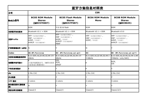
特需功能输入口 工作电压范围 预估价格范围
N 2.7 ~4.4v
N 2.7 ~4.4v
N 2.7 ~4.4v
N 2.7 ~4.4v
应用
适用于中端产品,如: 1,立体声耳机。 2,立体声迷你便携音箱。 3,汽车蓝牙套件。
适用于高端产品,如: 1,立体声耳机。 2,立体声迷你便携音箱。 3,汽车蓝牙套件。 4,大功率无线音箱。 可以实现: A,PCM信号的DSP处理。 B,RFID无线射频识别,非接触式的 自动识别,与NFC类似。 C,IOS设备可显示电池供电情况。 D,GAIA应用程序。
蓝牙方案信息对照表
公司 BC05 ROM Module Stereo (如BC57E687)
ROM 支持蓝牙协议版本 Bluetooth V2.1 + EDR HFP(电话通话音频流), HSP(电话功能控制), A2DP,(音乐流) AVRCP(音乐功能控制)
CSR BC05 Flash Module Stereo (如BC57F687)
6 capacitive touch sensor inputs 2.7 ~4.4v
Module型号
BC06 ROM Module Mono
ROM Bluetooth V2.1 + EDR HFP(电话通话音频流), HSP(电话功能控制), A2DP,(音乐流)
BC08 ROM Module Stereo (如BC8645)
ROM Bluetooth V3.0 HFP(电话通话音频流), HSP(电话功能控制), A2DP,(音乐流) AVRCP(音乐功能控制) Y SBC ,MP3,Faststream,AAC,aptStereo (如BC8670)
内置16M flash Bluetooth 4.0 HFP(电话通话音频流), HSP(电话功能控制), A2DP,(音乐流) AVRCP(音乐功能控制) PBAP Y SBC ,MP3,Faststream,AAC,apt-X 8,11.025,16,22.05,32,44.1,48 和96kHz(Only DAC) I2S, PCM, SPDIF Y 2 Mic CVC 2 3 colors Y Class1/2/3
STs8规格书
允许的最大波特率
ST 芯片的允许最大通信速率和 OSC 的频率有关。
OSC 频率值
芯片内部时钟
4M (典型值 R=15K,C=10PF) .25us
建议最大的波特率 20kbps
管脚说明
编号
名称
1
OSC
2
NC
I/O
I -
功能 外接电阻电容产生时钟 -
附录:
读取 STs8 芯片的示例程序,用 8051 汇编语言编写
ReadKey:
;;先发送 addr 寄存器的内容 C5H,做为 8bit 读命令
mov bitnum, #8
clr
sda ;;发送 start 信号
lcall Nop10 ;;延时
ReadKey_1:
东翎国际() 2008.11
7
CIN3
8
CIN4
9
CIN5
10
CIN6
11
CIN7
12
GND
13
CIN8
14
CIN9
15
CIN10
16
CIN11
17
CIN12
18
CIN13
19
CIN14
20
CIN15
21
SCL
22
SDA
23
INT
24
VDD
I
复位(低电平有效)
I
滑条0的感应电容输入
I
滑条1的感应电容输入
I
滑条2的感应电容输入
I
封装型式 ( SOP-24)
Generated by Foxit PDF Creator © Foxit Software For evaluation only.
TS08N_icpdf
Note 1 : Refer to 6.7 IMP_SEL (Sense Line Impedance) Implementation Note 2 : Refer to 6.4 SYNC/OPT implementation
Protection
VDD/GND VDD/GND VDD/GND VDD/GND
VDD VDD/GND VDD/GND VDD/GND VDD/GND VDD/GND VDD/GND VDD/GND VDD/GND VDD/GND
VDD/GND
VDD/GND
GND VDD/GND VDD/GND VDD/GND VDD/GND VDD/GND VDD/GND
ADSemiconductor Confidential 2 / 20
1 Specification
1.1 General Feature
8-Channel capacitive sensor with auto sensitivity calibration Selectable output operation (single or multi output mode) Low current consumption Uniformly adjustable 2 step sensitivity Sync function for parallel operation Adjustable internal frequency with external resister Selectable sense line impedance out of scanning Open-drain digital output Embedded common and normal noise elimination circuit RoHS compliant 24SOP and 32QFN package
奥伟斯科技为您提供ADS八通道触摸感应芯片TS08NC应用设计解决方案

TS08NC 八通道电容式传感器,带自动灵敏度校准功能TS08NC是韩国ADSEMI推出的一款经典电容式触摸感应IC,专注也电家控制器的应用。
随着电子信息技术的发展,电子元器件的功能逐渐多元化,智能化。
触摸芯片在现阶段的应用越来越多,涉及的领域也是越来越广泛。
目前电容触摸感应按键已经被广泛的应用于手机、VCD、便携式DVD、空调、冰箱、电磁炉、抽油烟机、洗衣机,微波炉、咖啡机、数码相框、液晶电视等产品,由于没有传统的按键,面板可以采用一个整块的面板,方便清洁,美观大方。
电容触摸感应按键的应用方式可以是按键开关,触摸板,滑动条和接近探测器。
深圳市奥伟斯科技有限公司是一家专注触摸芯片,单片机,电源管理芯片,语音芯片,场效应管,显示驱动芯片,网络接收芯片,运算放大器,红外线接收头及其它半导体产品的研发,代理销售推广的高新技术企业。
自成立以来一直致力于新半导体产品在国内的推广与销售,年销售额超过壹亿人民币,是一家具有综合竞争优势的专业电子元器件代理商。
主要品牌产品:一、OWEIS-TECH:OWEIS 触摸芯片、 OWEIS 接口芯片、 OWEIS 电源芯片、 OWEIS 语音芯片、 OWEIS 场效应管一、电容式触摸芯片、ADSEMI 触摸芯片代理、芯邦科技触控芯片、万代科技触摸按键芯片、博晶微触摸控制芯片、海栎创触摸感应芯片、启攀微触摸、 IC 融和微触摸感应、IC 合泰触摸按键、IC 通泰触摸芯片二、汽车电子/电源管理/接口芯片/逻辑芯片:IKSEMICON 一级代理、 ILN2003ADT、IK62783DT、 IL2596、IL2576 、ILX485、 ILX3485、 ILX232 、ILX3232三、功率器件/接收头/光电开关:KODENSHI、 AUK、 SMK系列、 MOS管、SMK0260F、 SMK0460F、SMK0760F、 SMK1260F、 SMK1820F、 SMK18T50F四、LED 显示驱动芯片:中微爱芯 AIP 系列: AIP1668、 AIP1628 、AIP1629 、AIP1616 、天微电子 TM 系列: TM1628 TM1668 TM1621五、电源管理芯片:Power Integrations LNK364PN LNK564PN 芯朋微 PN8012 PN8015 AP5054 AP5056 力生美晶源微友达天钰电子FR9886 FR9888六、语音芯片:APLUS 巨华电子AP23085 AP23170 AP23341 AP23682 AP89085 AP89170 AP89341 AP89341K AP89682七、运算放大器:3PEAK 运算放大器、聚洵运算放大器、圣邦微运算放大器八八、发光二极管:OSRAM 欧司朗发光二极管、Lite-On 光宝发光二极管、Everlight 亿光发光二极管、 Kingbright 今台发光二极管九、CAN收发器:NXP恩智浦CAN收发器、Microchip微芯CAN收发器十、分销产品线:ONSEMI安森美 TI德州仪器 ADI TOSHIBA东芝 AVAGO安华高十一、 MCU单片机ABOV现代单片机MC96F系列、 Microchip微芯单片机PIC12F PIC16F PIC18F系列、 FUJITSU富仕通单片机MB95F系列、STM单片机STM32F STM32L系列、 CKS中科芯单片机CKS32F系列、TI单片机 MSP430系列、TMS320F系列、 NXP单片机LPC系列下面,奥伟斯主要给大家详细介绍ADS八通道触摸按键芯片TS08NC的相关产品信息:1、Specification1.1 General Feature8-Channel capacitive sensor with auto sensitivity calibrationSelectable output operation (single or multi output mode) Low current consumptionUniformly adjustable 2 step sensitivitySync function for parallel operationAdjustable internal frequency with external resisterSelectable sense line impedance out of scanningOpen-drain digital outputEmbedded common and normal noise elimination circuitRoHS compliant 24SOP and 32QFN package1.2 ApplicationHome applicationMembrane switch replacementSealed control panels, keypadsDoor key-lock matrix applicationTouch screen replacement application2、Pin Description2.1 24SOP package2.2 32QFN package3、Absolute Maximum RatingBattery supply voltage 5.5VMaximum voltage on any pin VDD+0.3Maximum current on any PAD 100mAPower Dissipation 800mWStorage Temperature -50 ~ 150℃Operaing Temperature -20 ~ 75℃Junction Temperature 150℃Note :Unless any other command is noted, all above are operated in normal temperature.4、ESD & Latch-up Characteristics4.1 ESD Characteristics4.2 Latch-up Characteristics5、Electrical Characteristics (Prelimina)▪ VBDDBBB=3.3V, Rb=510k, (Unless otherwise noted), TBABBB = 25℃6、TS08N Implementation 6.1 R_BIAS implementation6.2 CS implementation6.3 CDEG implementation6.4 SYNC/OPT implementation 6.4.1 Single Connection6.4.2 Multi Connection6.5 RESET implementation6.6 Output Circuit Implementation6.7 IMP_SEL (Sense Line Impedance) Implementation7、Recommended Circuit Diagram7.1 Example – Power Line Split Strategy PCB LayoutA. Not split power Line (Bad power line design)B.Split power Line (One 5V regulator used) – RecommendedC.Split power Line (Separated 5V regulator used) –Strongly recommended8、MECHANICAL DRAWING8.1 Mechanical Drawing (24 SOP)8.2 Mechanical Drawing (32 QFN)9、MARKING DESCRIPTIONNOTES:LIFE SUPPORT POLICYAD SEMICONDUCTOR’S PRODUCTS ARE NOT AUTHORIZED FOR USE AS CRITICAL COMPONENTS IN LIFE SUPPORT DEVICES OR SYSTEMS WITHOUTTHE EXPRESS WRITTEN APPROVAL OF THE PRESIDENT AND GENERAL COUNSEL OF AD SEMICONDUCTOR CORPORATIONThe ADS logo is a registered trademark of ADSemiconductorⓒ 2015 ADSemiconductor – All Rights Reserved以上是“奥伟斯科技”分享的产品信息,如果您需要订购此款物料,请查看我们的官网与我们联系,非常感谢您的关注与支持!奥伟斯科技提供专业的智能电子锁触摸解决方案,并提供电子锁整套的芯片配套:低功耗触摸芯片低功耗单片机马达驱动芯片显示驱动芯片刷卡芯片时针芯片存储芯片语音芯片低压MOS管TVS二极管。
ANSG08SH韩国ADS八键触摸按键IC
8-Ch Auto Sensitivity Calibration Capacitive Touch Sensor(8-CH Auto Sensitivity Calibration Capacitive Touch Sensor)(8-CH Auto Sensitivity Calibration Capacitive Touch Sensor)(8-CH Auto Sensitivity Calibration Capacitive Touch Sensor)ANSG08QL (24 QFN)ANSG08SL (24 SOP) ANSG08SH (16 SOP)※Drawings not to scale(8-CH Auto Sensitivity Calibration Capacitive Touch Sensor)(8-CH Auto Sensitivity Calibration Capacitive Touch Sensor)(8-CH Auto Sensitivity Calibration Capacitive Touch Sensor)(8-CH Auto Sensitivity Calibration Capacitive Touch Sensor)(8-CH Auto Sensitivity Calibration Capacitive Touch Sensor)(8-CH Auto Sensitivity Calibration Capacitive Touch Sensor)(8-CH Auto Sensitivity Calibration Capacitive Touch Sensor)R S8R S1(8-CH Auto Sensitivity Calibration Capacitive Touch Sensor)(8-CH Auto Sensitivity Calibration Capacitive Touch Sensor)RR OUT2Ris 30kΩ typical.6.6Change initial reset register values (EEPROM writing)(8-CH Auto Sensitivity Calibration Capacitive Touch Sensor)(8-CH Auto Sensitivity Calibration Capacitive Touch Sensor)(8-CH Auto Sensitivity Calibration Capacitive Touch Sensor)ANSG08(8-CH Auto Sensitivity Calibration Capacitive Touch Sensor)7.7Transferring data7.7.1Write operationThe byte sequence is as follows:1.The first byte gives the device address plus the direction bit (R/W = 0).2.The second byte contains the internal address of the first register to be accessed.3.The next byte is written in the internal register. Following bytes are written in successiveinternal registers.4.The transfer lasts until stop conditions are encountered.5.The ANSG08 acknowledges every byte transfer.7.7.2Read operationThe address of the first register to read is programmed in a write operation without data, and terminated by the stop condition. Then, another start is followed by the device address and R/W= 1. All following bytes are now data to be read at successive positions starting from the initial address.7.7.3Read/Write Operation(8-CH Auto Sensitivity Calibration Capacitive Touch Sensor)(8-CH Auto Sensitivity Calibration Capacitive Touch Sensor)(8-CH Auto Sensitivity Calibration Capacitive Touch Sensor)(8-CH Auto Sensitivity Calibration Capacitive Touch Sensor)(8-CH Auto Sensitivity Calibration Capacitive Touch Sensor)(8-CH Auto Sensitivity Calibration Capacitive Touch Sensor)(8-CH Auto Sensitivity Calibration Capacitive Touch Sensor) RND channel up calibration speed at BF mode control bits.(8-CH Auto Sensitivity Calibration Capacitive Touch Sensor)(8-CH Auto Sensitivity Calibration Capacitive Touch Sensor)(8-CH Auto Sensitivity Calibration Capacitive Touch Sensor)Read channel indication register.The percent data of RND channel and sense channels.(8-CH Auto Sensitivity Calibration Capacitive Touch Sensor)(8-CH Auto Sensitivity Calibration Capacitive Touch Sensor)(8-CH Auto Sensitivity Calibration Capacitive Touch Sensor)ANSG08QL (24 QFN) Application Example CircuitANSG08QL is reset by internal reset circuit. VDD voltage rising time should be shorter than 100msec for proper operation.Normally, R.N.D pin dose not connection to anywhere. But, in radio frequency noiseR.N.D pin must form a pattern line on PCB.The VDD periodic voltage ripple over 50mV and the ripple frequency is lower than 10 kHz can cause sensitivity calibration. To prevent above problem, power (VDD, GND) line ofbe separated from other circuit. Especially LED driver power line or digital switching power line certainly should be treated to be separated from touch circuit.The CS patterns also should be routed as short as possible and the width of line might be about 0.25mm. Parallel capacitor of CS pin could be useful in case detail sensitivity mediation is required such as for complementation sensitivity difference between channels.Serial connection resistor of CS pins may be used to avoid mal-function from external surge and ESD. The capacitor that is between VDD and GND is an obligation. It should be located as close as possible from ANSG08QL.The CS pattern routing should be formed by bottom metal (opposite metal of touch PAD).ANSG08(8-CH Auto Sensitivity Calibration Capacitive Touch Sensor)9.2Example – Power Line Split Strategy PCB LayoutA. Not split power Line (Bad power line design)The noise that is generated by AC load or relay can be loaded at 5V power line.A big inductance might be appeared in case of the connection line between main board anddisplay board is too long, moreover the voltage ripple could be generated by LED (LCD) display driver at VDD (5V).B. Split power Line (One 5V regulator used) – RecommendedC. Split power Line (Separated 5V regulator used) – Strongly recommended(8-CH Auto Sensitivity Calibration Capacitive Touch Sensor)(8-CH Auto Sensitivity Calibration Capacitive Touch Sensor)(8-CH Auto Sensitivity Calibration Capacitive Touch Sensor)(8-CH Auto Sensitivity Calibration Capacitive Touch Sensor)(8-CH Auto Sensitivity Calibration Capacitive Touch Sensor)(8-CH Auto Sensitivity Calibration Capacitive Touch Sensor)。
C&C08交换机SM模块工作原理
C&C08交换机SM模块工作原理郭永彬【摘要】SM模块具有独立交换功能,可以完成模块内的呼叫接续,而模块间的呼叫则由各SM通过AM/CM来完成。
SM还提供分散数据库管理、呼叫处理、维护操作等各种功能,用户可以不通过AM/CM,通过串口直接在SM侧进行近端维护。
SM是C&C08数字程控交换机的核心,是各种业务接口的提供者,根据SM所提供的接口可把它分为纯用户模块(USM)、纯中继模块(TSM)、用户中继混装模块(UTM)三种类型。
USM(User Switch Module)只提供用户接口,TSM(Trunk Switch Module)只提供中继接口,UTM(User Trunk Module)提供用户和中继两种接口。
C&C08系统还有多种远端模块——RSM、RSMII、SMII,它们都可以看作SM的其他形式或者是附加于SM之上的功能块。
【期刊名称】《数字技术与应用》【年(卷),期】2010(000)005【总页数】2页(P158-159)【关键词】C&C08;交换模块;中继接口【作者】郭永彬【作者单位】中国联合网络通信有限公司德惠市分公司,吉林德惠130300【正文语种】中文【中图分类】TN9161 SM模块概述SM的机架在全局统一编号。
SM的模块号与SPM一起在1至160里编号。
SM 单模块局时模块号为1,机架号从1开始编。
SM的机框类型有:主控框、时钟框、用户框、DT框、AT框、RSA接口框,主控框占2个机框;当SM做单模块局时,还需配BAM框(内置式BAM)。
一个SM 机架有6 个机框,机框在本模块内统一编号,编号从0开始,由下向上、由近向远。
含有主控框的机架称为主机架,所有的SM都有且只有一个主机架,其它机架都称为副机架。
主机架中必须含有主控框,其他机框根据模块类型和需要来配置。
1.1 机框1.1.1 主控框SM的主控框是交换模块的控制中心和话路交换中心,负责整机的设备管理和接续控制。
腾龙2008智能型编程器使用说明.

腾龙2008智能型编程器使用说明隆重推出腾龙2008智能型编程器,采用电子开关电路取代跳线操作,操作变得更简单、更直接、更稳定。
腾龙2008同样继承本站超越飞越系列特点最大兼容。
支持所有的主板bios芯片、打印机复印机控制芯片、超值增加对PIC系列芯片的全面支持。
采用超线程MCU设计编程速度再次提高60%写入一片8M的芯片仅需要2分钟。
腾龙2008硬件版本为万用硬件版本的独特设计,全面兼容老版本和新版等等的硬件结构,独具时空切换功能,大家再也不会因为不清楚自己用的是什么硬件版本而发愁了。
独具时空切换的功能,可以同时支持PCB3控制软件和最新版控制软件,有些网友可能会感到奇怪,腾龙2008为什么要支持老的软件?原因其实很简单,因为新版软件0.99E,0.99E+等对W27C512和A T28C64B(程序存储器芯片,常用的单片机程序存储外置)等等芯片的支持的没有老版的98系列软件稳定,比如经典的97JA软件在烧写W27C512的成功律能达到100%,另外需要注意的一点是,站长本人在制作ICD2的过程中发现,0.97Ja烧写PIC16F877A的可靠性也是最一流的,而0.99e反倒不如0.97Ja那样完美,但是对于烧写BIOS芯片而言,0.98D2,0.98E等要更快一些。
腾龙2008编程器更新:硬件增加了对编程器过载保护、芯片插反保护、短路保护、软写入模式、电路。
采用3个微动开关选择编程电压,从此不再需要去记忆繁琐的跳线。
软件采用0.99E烧写芯片的速度提高30%。
腾龙2008编程器支持所有的主板BIOS芯片、独家提供对内存SPD芯片、彩电显示器EPROM芯片、打印机复印机控制芯片的完美支持。
唯我忠于维修级编程器开发,腾龙2008编程器于其他网站设计的编程器不同,我们的产品定位在计算机芯片级维修行业,不论是硬件设计还是软件都遵循实用性第一的方针,腾龙2008编程器是一款专业的维修设备。
彻底抛弃DC供电,采用单USB供电设计,工作更稳定专业设计的升压电路可将USB供电提升至35V。
8通道触摸感应按钮芯片规格书-LH828A
8键触摸检测IC(8 KEYS TOUCH PAD DETECTOR IC)1.0概述LH828A是一款电容感应8触摸键检测(touch pad detector)IC。
触摸检测IC 将取代传统的机械开关和按钮键。
人机界面控制面板通过非导电介质材料,能够稳定检测人体的感应。
同时具有低功耗和宽工作电压范围。
2.0特点◆工作电压 2.0V~5.5V◆工作电流在VDD=3V时典型值80uA, 最大值160uA◆输出刷新率在VDD=3V时约55Hz◆64级可选灵敏度 (SLSE0~5管脚选项)另外提供2种基阶(base-step) (OPST管脚选项)◆稳定的人体接触检测,以取代传统直接切换的键(direct switch key)◆提供直接(direct)模式、矩阵(matrix)模式和串行(serial)模式,由pad选项选择◆直接模式下最多8个输入pad和8个输出;串行接口模式下最多8个输入pad;固定的2*4和3*3矩阵类型提供最多8个输入pads◆输出可由pad选项选择为高电平有效或低电平有效◆在上电之后有3.5~4秒的稳定时间,在此期间不要触摸键区(key-pad),且功能无效3.0 应用◆广泛的消费性产品◆防水电器◆取代按钮键4.0 封装结构5.0 接口形式5.1直接(DIRECT)模式框图:5.2串行接口(SERIAL INTERFACE)模式框图:5.3键矩阵(KEY-MATRIX)模式框图:6.0 管脚描述管脚号 管脚名称共用管脚I/O类型管脚描述1 OSC2 I/O 传感器振荡器2 TOPAD I 此为输入口内部公共点(common point )3 I7 I 输入口4 I6 I 输入口5 NC6 NC7 NC8 I5 I 输入口9 I4 I 输入口10 I3 I 输入口11 I2 I 输入口12 I1 I 输入口13 I0 I 输入口14 OPW0 I-PH OPW0~1 均为选择键检测windows 的选项管脚15 OPW1 I-PH OPW0~1 均为选择键检测windows 的选项管脚16 OPT0 I-PH OPT0~1 均为选择键接通时间的选项管脚17 NC18 OPT1 I-PH OPT0~1 均为选择键接通时间的选项管脚19 NC20 NC21 OSC1 I/O 系统振荡器管脚22 VSS P 负电源电压,接地23 VDD P 正电源电压24 OPS1 I-PH 输出类型选项管脚25 OPS0 I-PH 输出类型选项管脚26 AHL I-PH 选择输出为高电平有效或低电平有效27 TEST I-PH 仅用于测试,实际应用时必需连接到VSS.28 Q0 (DO/SCN0) I/O Q0 为直接模式下的输出管脚DO 为串行模式下的移位数据输出SCN0 为矩阵模式下的第一个扫描(scanning)管脚29 Q1 (SCN1) I/O Q1 为直接模式下的输出管脚SCN1 为矩阵模式下的第二个扫描(scanning)管脚30 NC31 OPST I-PH 选择灵敏度的基阶(base step)32 NC33 Q2 (SCN2) I/O Q2 为直接模式下的输出管脚SCN2 为矩阵模式下的第三个扫描(scanning)管脚34 Q3 (SCN3) I/O Q3 为直接模式下的输出管脚SCN3 为矩阵模式下的第四个扫描(scanning)管脚35 Q4 (SCN4) I/O Q4 为直接模式下的输出管脚SCN4 为矩阵模式下的第五个扫描(scanning)管脚36 Q5 (SCN5) I/O Q5 为直接模式下的输出管脚SCN5 为矩阵模式下的第六个扫描(scanning)管脚37 Q6 (RST) I/O Q6 为直接模式下的输出管脚RST 为串行模式下的复位输入管脚38 Q7 (CK) I/O Q7 为直接模式下的输出管脚CK 为串行模式下的时钟输入管脚39 DV O (表示)数据有效的输出信号40 VSS P 负电源电压,接地41 SLSE0 I-PH SLSE0~5 均为选择灵敏度的选项管脚42 NC43 SLSE1 I-PH SLSE0~5 均为选择灵敏度的选项管脚44 NC45 SLSE2 I-PH SLSE0~5 均为选择灵敏度的选项管脚46 SLSE3 I-PH SLSE0~5 均为选择灵敏度的选项管脚47 SLSE4 I-PH SLSE0~5 均为选择灵敏度的选项管脚48 SLSE5 I-PH SLSE0~5 均为选择灵敏度的选项管脚说明: CK 和RST 输入带保护电阻,为避免输出冲突。
AN0828 电容触摸库说明书

AN0828: Capacitive Sensing Library Overviewcluding all the features and algorithms required to make a capaci-tive sensing product.The capacitive sensing library includes the following:•Scanning routines that buffer raw samples.•Filters that process and shape raw data.•Baselining routines that maintain an expected inactive sensor capacitive value.•Threshold detection routines that qualify touches using application-defined thresh-olds, choosing between filtered data types dynamically depending on the system’ssignal to noise ratio.•Interference characterization routines used to control touch qualification.•Low power control routines that transition the system between active mode and lowpower Sleep mode.1. OverviewThis document and the library refer to the electrode connected to a capacitive sensing input pin on a Silicon Labs MCU as a sensor. A sensor whose capacitance is in an off state, where no conductive object is in proximity to that sensor, is called inactive. The inactive state is qualified by comparing the output of the sensor to an inactive threshold maintained by the library. Firmware qualifies a sensor as active when output crosses an active threshold maintained by the library.An inactive sensor’scapacitance crosses activethreshold and persists abovethreshold for successivesamples, causing the library toBaseline valueprovides runtime expected inactive value for a sensorAn active sensor’s capacitance crosses inactive threshold and persists below, causing the library to qualify the sensor as ‘inactive’The library defines both thresholds relative to thesensor’s baselineActivethresholdInactivethresholdFigure 1.1. Basic Library FunctionalityThe library also includes low power features that enable the system to switch between an active mode, where sensors are either active or have been active in the recent past, and sleep mode, which configures the MCU to its lowest power, wake-on-touch state. This docu-ment covers the configuration of the library as well as the APIs and data structures the library exposes and maintains for access by an application layer of firmware.The capacitive sensing library is available on EFM32 devices and 8-bit devices with the capacitive sensing module (EFM8SB1, C8051F99x, and C8051F97x). See AN0028: Low Energy Sensor Interface — Capacitive Sense for more information on the EFM32 hardware capacitive sense implementation.OverviewCapacitive Sensing Project Structure Overview 2. Capacitive Sensing Project Structure OverviewThe capacitive sensing project structure’s design enables users to drop their own routines and functionality into an existing project with minimal editing of source code and other predesigned components. The basic project structure is shown in the figure below.Figure 2.1. System OverviewThe following sections describe each of these components in greater detail. A review of this structure helps to fully understand how hardware resources are being allocated. However, to concentrate only on capacitive sensing configuration, see AN0829: Capacitive Sensing Library Configuration Guide. Application notes can be found on the Silicon Labs website (/8bit-appnotes) and in Simplicity Studio. The firmware examples included with Simplicity Studio use the naming conventions in the above figure and throughout this document.For EFM32 examples, the configuration of the hardware block is slightly different from the 8-bit implementation, though similar in struc-ture. See the examples included in Simplicity Studio v4 (Gecko SDK v4.4.0 or later) for more information.This layer of a capacitive sensing project is the primary place to add application-specific code. The main() routine is located in this sec-tion. In the example files, the profiler_interface.c/h routines provide an example of how code can interface with the library data structures to output capacitive sensing information. The protocol created by profiler_interface.c is compatible with Simplicity Stu-dio's Capacitive Sensing Profiler and enables realtime display of capacitive sensing output and library-maintained variables. Board ex-amples included with Simplicity Studio show how touch detection can control the state of LEDs and other features.The main() routine includes the top-level calls into the capacitive sensing API. Calls initialize capacitive-sensing controlled hardware and capacitive sensing state variables before entering a while(1) loop where the library’s functionality is exercised through CSLIB_upd ate(). A call to the low-power state machine is also present, although this call can be removed if low-power features have not been enabled.Note that the application layer must include function definitions for a set of callback routines used by the library. The requirements for these functions are discussed in 7. Library Execution and Data Access.The Simplicity Studio code examples include a file group called the Comm Interface. The code in that interface provides one example of how data can be retrieved from the Capacitive Sensing Library data structures to be output through a serial interface. Also, the protocol used by the examples is specially formatted for the Capacitive Sense Profiler. For a description of that protocol, see AN0829.5. Sensing Config FilesThe Configuration Files layer includes the files listed in the table below; each file has a specific function. Note that Simplicity Studio's hardware configurator provides capacitive sensing firmware library configuration support for capacitive sensing-enabled MCUs. For supported MCUs, we suggest configuring and generating capacitive sensing projects through that tool instead of editing files manually as described in the sections below.Table 5.1. Config Layer Files5.1 Values in ProjectConfig.hThe table below lists the definitions found in cslib_config.h, their meanings, and suggested values.Table 5.2. cslib_config.h DefinitionsThe library's usage of the timer and low power configuration functions are shown in Figure 5.1 State Machine Operation with FREE_RUN_SETTING = 1 on page 8 and Figure 5.2 State Machine Operation with FREE_RUN_SETTING = 0 on page 9.Figure 5.1. State Machine Operation with FREE_RUN_SETTING = 1Figure 5.2 State Machine Operation with FREE_RUN_SETTING = 0 on page 9shows operation of the low-power state machine when using the ACTIVE_MODE_ACTIVE_TIMER mode.Figure 5.2. State Machine Operation with FREE_RUN_SETTING = 05.2 Processed Data ArrayThe data processing filter runs a dejitter algorithm and saves the output into the processed data buffer for that channel. The dejitter algorithm behaves as shown in the figure below. A sensor’s new value is not saved to the processed data buffer unless that value falls outside of an envelope surrounding the previous value that has been defined at compile time.Figure 5.3. Dejitter AlgorithmThis algorithm is useful for routines that benefit from a steady capacitive sensing output, when small variations in raw output are not necessary for processing. In a low-noise environment, this processing algorithm yields a high degree of responsiveness. An example of the effect of the de-jitter processing can be seen in the chart below. Note that the algorithm tracks a 200-code touch but ignores the minor variations in untouched and touched capacitive sensing output.Figure 5.4. Dejitter Filter Response Example5.3 Exponential Averaged ValuesThe exponential averaging filter provides a filter for higher noise environments. The algorithm uses a form of exponential averaging described by the following equation:Y[n]=(1exp.av.constant ×x[n])+(exp.av.constant–1exp.av.constant×y[n–1])The exponential averaging constant is 64, which provides a balance between aggressive filtering and acceptable response time for 1–40 sensors when DEF_FREE_RUN_SETTING = 1. This filter will result in a touch detection that has a slower response time than the other filters included in the algorithm, but the exponentially averaged output is more reliable than the other filter options in terms of filtering out false positive events. Note that each sensor’s exponentially-averaged value is stored in a 4-byte variable in the sensor node structure. In this variable, the upper 2 bytes show the averaged value, analogous to the 2-byte raw or processed values for that sensor. The lower 2 bytes preserve LSBs from the division inherent in the averaging filter and yield more reliable results from the filter.6. Touch QualificationThe library characterizes activity on a sensor using hysteresis and debouncing to screen out false-positive events. The algorithm uses inactive and active thresholds defined above baseline as shown in Figure 6.1 Derivation of Touch Delta for a Sensor on page 12 and Figure 6.2 Derivation of Active and Inactive Thresholds for a Sensor on page 13. The debounce state machine used by the algorithm is defined in Figure 6.3 Threshold Detection State Machine on page 14, and a visual representation of the state machine is included in Figure 6.4 Example Threshold Detection State Machine Processing on page 15.Figure 6.1. Derivation of Touch Delta for a SensorActivethresholdInactivethresholdThresholds defined relative tobaseline byDEF_ACTIVE_SENSOR_DELTA andDEF_INACTIVE_SENSOR_DELTArespectivelyFigure 6.2. Derivation of Active and Inactive Thresholds for a SensorOnce the algorithm derives the touch delta and thresholds for the sensor, the function analyzes the position of the newest sensor data relative to the thresholds, and updates the sensor’s state information saved in debounce_active_count and debounce_inactive_count to derive the new threshold state. The threshold state determination state machine executes as described in the figure below.Figure 6.3. Threshold Detection State MachineThe figure below shows the process of qualifying a new touch event. Note that the debounce_active_count begins incrementing when the capacitive sensing values cross the active threshold, and the event is not qualified as an active sensor until a set number of consec-utive sensor samples above threshold have occurred. In this example, BUTTON_DEBOUNCE is set to a value of 3, and the data used in the threshold detection function consists of processed, de-jittered samples.128012301180113010801030980C a p a c i t i v e s e n s i n g o u t p u t c o d e s1 2 3 4 5 6 7 8 9 10 11 12Debounce value Active threshold120123Inactive thresholdTouch qualified on this samplesampleFigure 6.4. Example Threshold Detection State Machine Processing7. Library Execution and Data AccessThe library executes code in the foreground rather than backgrounding algorithms in asynchronous interrupts. Because code executes in the foreground, the application layer must call a few routines to scan sensors, process data, and update the system’s state.The Simplicity Studio code examples contain a main.c routine that shows the suggested coding structure and placement of the top-level library APIs. Initialization of the library occurs after reset by calling CSLIB_initHardware()and CSLIB_initLibrary(). These two functions initialize all library state variables and technology-specific hardware. For more information on allocated hardware, see the sec-tions below called capacitive sensing hardware callback routines and low power and timer configuration callback routines.Inside the main()routine’s while(1)loop, the function CSLIB_update()updates the library’s state. CSLIB_update()executes all scanning, processing, and touch qualification. After that function returns, the library’s data structures have been updated and new data is ready to for use by the application layer code.Also in the while(1) look is the function CSLIB_lowPowerUpdate(), which controls the power state of the MCU depending on settings in cslib_config.h. Without this call in the build, the system will not be able to enter its sleep mode.7.1 Sensor Data StructureThe library saves the state of all defined sensors in a data structure defined in CSLibrary.h as the SensorNode struct. The contents of that structure are defined in the table below.Table 7.1. SensorNode Data Structure Contents7.2 Data Access APIsThe library includes some functions to streamline access of some commonly examined variables in the sensor node structure. Each available function is described in the table below. Like the declaration for the sensor node structure, these functions are also declared inside cslib.h.Table 7.2. Data Access API Functions7.3 Capacitive Sensing Hardware Callback FunctionsThe library relies on a set of callback routines defined outside the pre-compiled library that are responsible for capacitive sensing and low-power control. The declarations for these functions are found in hardware_routines.h and low_power_config.h.The following sections list all capacitive sensing-related callback routines and their requirements. The tables also define the level of modularity of each routine. Function means that changes will need to be made to the function body to meet the requirements of each application. Struct means that the function body won’t need to be changed, but changes will need to be made to the contents of the technology-specifc struct provided by the template and example files used to configure the capacitive sensor. Technology means that the functions should not need to be changed across applications, and must only be replaced by other template/example files for differ-ent sensing technologies.Table 7.3. Callback Routines in hardware_routines.c7.4 Low Power and Timer Configuration Callback RoutinesThe capacitive sensing library makes calls into routines to configure for low power mode, and those calls must be defined in the project’s source code. Additionally, the library needs a time base for sensing and for low power timing, and those functions must be defined in source as well. Fortunately, most of these files can be lifted from the examples and template projects as-is.Table 7.4. Callback Routines in low_power_config.c7.5 Info Array ContentsThe library includes a function called uint8_t* CSLIB_getInfoArrayPointer(), which returns a pointer to an array of bytes describ-ing the characteristics of the library. The first two bytes of the array indicate the version of the library. Based on the version number, firmware can know the total size of the array and what the other contents mean. The version number can be decoded as shown in the table below.Table 7.5. Byte Number and ContentsThe information array structure is defined version-by-version. For version 1.0 of the library, the information array contains no other con-tents.8. Revision History8.1 Revision 0.32016-10-14Added EFM32 to 1. Overview.Added mention of EFM32 to 2. Capacitive Sensing Project Structure Overview.8.2 Revision 0.22015-02-13Updated formatting.8.3 Revision 0.12014-06-13Initial revision.AN0828: Capacitive Sensing Library OverviewRevision History Silicon Laboratories Inc.400 West Cesar Chavez Austin, TX 78701USASimplicity StudioOne-click access to MCU andwireless tools, documentation,software, source code libraries &more. Available for Windows,Mac and Linux!IoT Portfolio /IoT SW/HW /simplicity Quality /quality Support and CommunityDisclaimer Silicon Labs intends to provide customers with the latest, accurate, and in-depth documentation of all peripherals and modules available for system and software implementers using or intending to use the Silicon Labs products. Characterization data, available modules and peripherals, memory sizes and memory addresses refer to each specific device, and "Typical" parameters provided can and do vary in different applications. Application examples described herein are for illustrative purposes only. Silicon Labs reserves the right to make changes without further notice and limitation to product information, specifications, and descriptions herein, and does not give warranties as to the accuracy or completeness of the included information. Silicon Labs shall have no liability for the consequences of use of the information supplied herein. This document does not imply or express copyright licenses granted hereunder to design or fabricate any integrated circuits. The products are not designed or authorized to be used within any Life Support System without the specific written consent of Silicon Labs. A "Life Support System" is any product or system intended to support or sustain life and/or health, which, if it fails, can be reasonably expected to result in significant personal injury or death. Silicon Labs products are not designed or authorized for military applications. Silicon Labs products shall under no circumstances be used in weapons of mass destruction including (but not limited to) nuclear, biological or chemical weapons, or missiles capable of delivering such weapons.Trademark Information Silicon Laboratories Inc.® , Silicon Laboratories®, Silicon Labs®, SiLabs® and the Silicon Labs logo®, Bluegiga®, Bluegiga Logo®, Clockbuilder®, CMEMS®, DSPLL®, EFM®, EFM32®, EFR, Ember®, Energy Micro, Energy Micro logo and combinations thereof, "the world’s most energy friendly microcontrollers", Ember®, EZLink®, EZRadio®, EZRadioPRO®, Gecko®, ISOmodem®, Precision32®, ProSLIC®, Simplicity Studio®, SiPHY®, Telegesis, the Telegesis Logo®, USBXpress® and others are trademarks or registered trademarks of Silicon Labs. ARM, CORTEX, Cortex-M3 and THUMB are trademarks or registered trademarks of ARM Holdings. Keil is a registered trademark of ARM Limited. All other products or brand names mentioned herein are trademarks of their respective holders.。
DLT8T10S十通道电容式触摸感应控制芯片规格书

DLT8T10S十通道电容式触摸感应控制芯片规格书DLT8T10S十通道电容式触摸感应控制芯片10.PCB布线注意事项1)触摸按键板尽量单独布板,这样可以降低干扰。
2)触摸按键到触摸芯片的走线距离越短越好。
3)使用双面PCB,可以在顶层使用圆形、方形等作为触摸感应PAD,从触摸感应PAD到IC管脚的连线应该尽量走在触摸感应PAD的另外一面。
同时连线应该尽量走细,不要绕远。
使用单面板则一般需要使用感应弹簧片。
4)触摸按键到触摸芯片的走线的间距大于1mm为佳,走线中绝对不能有其它的信号线穿过或者交叉,也不要从触摸IC的底部穿过。
5)触摸按键的铜皮的背面不要走线,以免干扰。
6)触摸按键面积的大小,以触摸体的接触面积相同为最佳,如果厚度塑胶在2mm左右,建议触摸PAD的面积在1212mm左右。
过大容易产生干扰,过小容易灵敏度不够。
7)触摸按键的面积与绝缘体的厚度都会影响到灵敏度,一般建议绝缘体的厚度以不超过3mm为最佳。
8)触摸按键的最小面积建议不小于55mm,但要视绝缘材料材质和厚度而定。
9)触摸按键之间或触摸按键与元器件之间的最小距离以不小于4mm为最佳,如灵敏度调高则间距相对需要增加。
10)双面板触摸感应PAD的周围与背面一般建议不铺地,触摸感应PAD与PAD之间尽量避免不同PAD之平行引线距离过近,这些都能降低触摸按键的灵敏度。
11)因为空气介电常数太小,并且受湿度影响,所以介质中最好不要有空气。
触摸PAD或者感应弹簧片与绝缘外壳应压合紧密,保持平整,以免有气隙产生。
外壳与PAD之间可以采用非导电胶进行粘和,例如压克力胶3MHBM系列。
12)灵敏度电容建议使用温度系数小精度高的电容,以免造成灵敏度不一致或随温度变化而变化。
一般插件电容建议5%精度涤纶电容,如需贴片电容则建议使用10%或更高精度的NPO材质电容或X7R材质电容。
※注意:规格如有更新﹐恕不另行通知。
请在使用该IC前更新规格书至最新版本。
stm8引脚能否做成触摸输入

stm8 引脚能否做成触摸输入
我曾开发带有触摸按键功能的消费类电子产品,在起初也是不知道STM8 引脚可以实现触摸这个功能,所以这里写给大家。
1
写在前面
我们开发带有触摸功能的产品时,可能首先考虑的就是购买一个触摸芯片。
但是对于消费类电子,如果你的产量较大,可能就会考虑这1,2 块的触摸芯片的成本。
此时,使用STM8,或者STM32 作为主控的IC 可以实现触摸功能就显得比较重要了。
由于很多人不知道这个功能,这里先让大家了解并熟悉这一项触摸按键功能。
2。
韩国ADS公司的TS08P触摸IC用法总结

我在广州先导视讯工作的时候,用到这款触摸IC,感觉不错,把自己的经验总结以下:TS08P韩国ADS八键触摸按键IC芯片型号:TS08P封装及用法如下:工作电压2.5V~5V用法一:触点大小是:10*7(毫米)When active high is selected TS08P outputs are low in normal state and become high in touch detect state. 当你选择高电平输出时,平时输出是低电平,当触点被触摸输出就会变高电平When TS08P is used as active low output, the level of normal state is high and that of touch detect is low. 当你选择低电平输出时,平时输出是高电平,当触点被触摸输出就会变低电平数字电平输出:1、8个按键,电平模式输出(高电平、电平),由7引脚SYNC4设定,SYNC4接VDD时为高电平输出,NC时是低电平输出。
接地时,是另外的用法(模拟电压输出),见用法二。
2、按键是单通道单输出还是双通道单输出由SYNC3设定,SYNC3接VDD为单单,NC为双单,接GND为多通道输出。
SYNC1和SYNC2两者共同设定介质的厚度(也就是灵敏度设定)1、输出是开漏的所以要上拉,上拉电阻10K2、内部校准速度设定,由SYNC5设定,VDD快,GND慢,NC正常。
用法二,模拟电压输出TS08P has internal analog output circuit and all the output of CS can be express as analog voltage value using only two output ports (OUT1, OUT8). TS08P中只使用两个输出端口(OUT1,OUT8)才具有:内部模拟输出电路和所有触点可以表达为模拟的输出只使用两个输出端口(OUT1,OUT8)。
基于STM8单片机的手势识别器控制电路设计
基于STM8单片机的手势识别器控制电路设计
于姣
【期刊名称】《电声技术》
【年(卷),期】2022(46)9
【摘要】为了满足在非接触式环境中依然可以敏捷、准确地操作,人机交互手势识别设备在各领域广泛应用。
设计一种基于STM8单片机的手势识别器,利用非接触式电容传感器与单片覆铜板相连接,实时掌握设备电容值的具体变化。
将STM8单片机作为此设备的主控制器,设计电源转换电路、语音提示电路,实现测试者将手部与覆铜板测试区域靠近时,传感器上所显示的数值就会有所变化。
设计引入卡尔曼滤波算法,通过多次训练手势识别,提高电容示值的实时性、稳定性。
最后对设计的手势识别器进行系统测试,对四通道手掌型的测试结果表明,其可以满足“猜拳、划拳、人机大战”等多样手势功能,且设备鲁棒性与测试满意度提升,对手部动作的识别准确率较高,稳定运行且满足实时性要求,证明了设计思路的推广可行性。
【总页数】4页(P141-144)
【作者】于姣
【作者单位】苏州高等职业技术学校
【正文语种】中文
【中图分类】TP311
【相关文献】
1.一款基于STM8S系列单片机的洗碗机控制器设计及实现
2.基于STM8单片机可移动智能风扇控制器系统设计
3.一款基于STM8S系列单片机的洗碗机控制器设计及实现
4.基于STM8单片机激光控制器的设计
5.基于STM8单片机手势识别器控制电路设计
因版权原因,仅展示原文概要,查看原文内容请购买。