骏达电子工程设计资料
电子行业的电路板设计资料
电子行业的电路板设计资料在当今数字化时代,电子行业发展迅猛。
电路板是电子设备中不可或缺的组成部分,负责电气信号的传输和控制。
为了确保电子设备的可靠性和性能,电路板的设计十分重要。
本文将详细介绍电子行业中电路板设计所需的资料。
一、器件数据表格在电路板设计过程中,需要使用各种电子元件,如电阻、电容、二极管等。
为了准确设计电路板,我们需要准备每个元件的数据表格。
数据表格包含了元件的基本参数,例如电阻的阻值、电容的容值、二极管的导通电压等。
通过仔细研究这些数据表格,设计师可以选择最适合的元件,确保电路板的工作性能。
二、CAD软件电路板设计是一项复杂的任务,需要使用计算机辅助设计(Computer-Aided Design,CAD)软件。
这些软件提供了功能强大的工具,可以帮助设计师绘制和布局电路板。
通过CAD软件,设计师可以精确安排元件的位置、绘制电路连接线路以及进行电路仿真。
常用的CAD软件包括Altium Designer、Cadence Allegro等。
三、电路板尺寸要求不同的电子设备对电路板的尺寸要求各异。
在电路板设计过程中,需要事先确定电路板的尺寸。
这可以依据电子设备的尺寸、功能需求以及外观设计来确定。
设计师需要准确测量并记录电子设备的尺寸,并在CAD软件中设置相应的参数,以确保设计出满足要求的电路板。
四、电路板层次和堆叠方式电路板可采用单面、双面或多层堆叠等不同的布线方式。
设计师需要根据电子设备的复杂程度和电路的布局要求,选择合适的电路板层次和堆叠方式。
例如,高端通信设备通常使用多层堆叠电路板,以实现更多的功能和更高的集成度。
通过合理选择电路板的层次和堆叠方式,可以提高电子设备的性能和可靠性。
五、设计规范与标准在电路板设计过程中,需要遵循一系列的设计规范与标准。
这些规范和标准包括电路板的最佳布局、电子元件的最小间距、导线的最大电流容量等。
通过遵循这些规范和标准,可以确保电路板的设计符合工业标准,避免潜在的电路故障和不稳定性。
MAS3504D资料
MAS3504DContentsPage Section Title4 1.Introduction4 1.1.Features5 1.2.Application Overview5 1.2.1.Decoder Mode5 1.2.2.Encoder Mode6 2.Functional Description of the MAS3504D6 2.1.DSP Core6 2.2.Firmware (Internal Program ROM)6 2.2.1.G.729 Encoder6 2.2.2.G.729 Decoder6 2.3.Program Download Feature6 2.4.Clock Management6 2.5.Power Supply Concept6 2.5.1.Internal Voltage Monitor7 2.5.2.DC/DC Converter7 2.5.3.Stand-by Functions8 2.5.4.Start-up Sequence8 2.6.Interfaces8 2.6.1.Parallel Input Output Interface (PIO)8 2.6.2.Parallel Data Output9 2.6.3.Parallel Data Input9 2.6.3.1.DMA Handshake Protocol10 2.6.3.2.End of DMA Transfer10 2.6.4.Audio Input Interface (SDI)10 2.6.5.Audio Output Interface (SDO)11 2.6.5.1.Example 1:16 Bits/Sample (I2S Compatible Data Format) 11 2.6.5.2.Example 2:32 Bit/Sample (Inverted SOI)12 3.Control Interfaces12 3.1.I2C Bus Interface12 3.1.1.Device address and Subaddresses13 mand Structure13 3.2.1.Conventions for the Command Description14 3.3.Detailed MAS3504D Command Syntax14 3.3.1.Run14 3.3.2.Write Register14 3.3.3.Write D0 Memory14 3.3.4.Write D1 Memory15 3.3.5.Read Register15 3.3.6.Read D0 Memory15 3.3.7.Read D1 Memory16 3.4.Version Number16 3.5.Register Table16 3.5.1.DC/DC Converter (Reg. 8E hex)16 er Control (Reg. FD hex)17 3.5.2.1.Data Transmission FormatMAS3504DContents, continuedPage Section Title17 3.5.2.2.Encoder Operation17 3.5.2.3.Decoder Operation18 3.5.2.4.Pause and Mute18 3.5.3.Volume Control (Reg. FC hex)18 3.5.4.Interface Control18 3.5.4.1.Wordlength Control (Reg. 74hex)18 3.5.4.2.Input Configuration (Reg. 61hex)18 3.5.4.3.Output Configuration (Reg. E1hex)18 3.5.5.Hardware Control (Reg. FA hex)22 4.Specifications22 4.1.Outline Dimensions23 4.2.Pin Connections and Short Descriptions25 4.2.1.Pin Descriptions25 4.2.1.1.Power Supply Pins25 4.2.1.2.DC/DC Converter Pins25 4.2.1.3.Control Lines25 4.2.1.4.Parallel Interface Lines25 4.2.1.4.1.PIO Handshake Lines25 4.2.1.4.2.PIO Data Lines26 4.2.1.5.Voltage Supervision And Other Functions26 4.2.1.6.Serial Input Interface26 4.2.1.7.Serial Output Interface26 4.2.1.8.Miscellaneous26 4.2.2.Pin Configurations27 4.2.3.Internal Pin Circuits28 4.2.4.Electrical Characteristics28 4.2.4.1.Absolute Maximum Ratings29 4.2.4.2.Recommended Operating Conditions30 4.2.4.3.Characteristics31 4.2.4.3.1.I2C Characteristics32 4.2.4.3.2.I2S Bus Characteristics – SDI33 4.2.4.3.3.I2S Characteristics – SDO34 4.2.4.4.DC/DC Converter Characteristics36 4.2.4.5.Typical Performance Characteristics40 5.Data Sheet HistoryLicense NoticeSupply of this implementation of G.729A technology does not convey a license nor imply any right to use this imple-mentation in any finished end-user or ready-to-use final product. An independant license for such use is required. For information on such license agreement please contact:Sipro Lab Telecom Inc.email: patriciam@Fax: +1 (514) 737-2327MAS3504DG.729 Annex A Voice Codec1.IntroductionThe MAS3504D is a single-chip codec for use in memory-based voice recording and playback applica-tions. Due to embedded memories, the embedded DC/ DC up-converter, and the very low power consump-tion, the MAS3504D is ideally suited for portable elec-tronics.The MAS3504D implements a voice encoder and decoder that is compliant to the ITU Standard G.729 Annex A. This standard works on 8kHz, 16bit, mono audio data that is compressed to 1bit per audio sam-ple. One second of compressed audio data uses 1000bytes of memory.1.1.Features–Single-chip G.729 decoder–G.729 Annex A encoder–ITU compliance tests passed–Parallel input and parallel output of coded bitstream data–Input audio data read from an I2S bus (in various formats)–Output audio data delivered via an I2S bus (in vari-ous formats)–Digital volume / mute–Low power dissipation (150mW for encoder, 80mW for decoder @ 3.3V)–Supply voltage range: 1.0V to 3.6V due to built-in DC/DC converter (1-cell battery operation)–Adjustable power supply supervision–Power-off function–Additional functionality achievable via download software (ADPCM encoder/decoder)Fig. 1–1:MAS3504D block diagramMAS 3504D1.2.Application OverviewThe MAS 3504D can be applied in two major environ-ments: as standalone decoder or as encoder/decoder combination. For decoding only mode, the DAC 3550A fits perfectly to the requirements of the MAS 3504D. It is a high-quality multi sample rate DAC (8kHz..50kHz) with internal crystal oscillator, which is only needed for generating the decoder Clock, and inte-grated stereo headphone amplifier plus two stereo inputs.1.2.1.Decoder ModeIn a memory-based voice playback environment, the decoding is started with a command from a controller.Then the MAS 3504D continuously requests frames of G.729 data every 10ms via the parallel (PIO) inter-face.A delayed response of the host to the request signal (max. 20milliseconds) will be tolerated by the MAS 3504D as long as the input buffer does not run empty. A PC might use its DMA capabilities to transfer the data in the background to the MAS 3504D without interfering with its foreground processes.The source of the bit stream may be a memory (e.g.ROM, Flash) or PC peripherals, such as CD-ROM drive, a hard disk or a floppy disk drive.1.2.2.Encoder ModeFor encoding a support routine must be downloaded to the MAS 3504D via I 2C. After the encoder is started, it begins to encode the incoming audio data and writes the coded datastream to the parallel (PIO) interface. A delayed response of the host to the data available signal (max. 20milliseconds) will be tolerated by the MAS 3504D as long as the output buffer does not overrun.Fig. 1–2:Block diagram of a MAS 3504D, decoding a stored bit stream in a decoding only applicationFig. 1–3:Block diagram of a MAS 3504D in an encoding/decoding applicationROM, CD-ROM, RAM, Flash Mem. ..Host (PC, Controller)I 2Sline outI 2Cdemand signal demand clock G.729 bit streamCLKI CLKOUT18.432MHz MAS 3504DDAC 3550AROM, CD-ROM, RAM, Flash Mem. ..Host (PC, Controller)clockline in I 2CCLKIG.729 bit streamMic in Handshake signals line outstrobe data outdata in I 2S linesMAS 3504DPLLAD/DAMAS3504D2.Functional Description2.1.DSP CoreThe hardware of the MAS3504D consists of a high performance Digital Signal Processor and appropriate interfaces. The processor works with a memory word length of 20bits and an extended range of 32bits in its accumulators. The instruction set of the DSP is highly optimized for audio data compression and decompres-sion. Thus, only very small areas of internal RAM and ROM are required. All data input and output actions are based on a ‘non cycle stealing’ background DMA that does not cause any computational overhead.2.2.Firmware (Internal Program ROM)The firmware fully contains a G.729 voice decoder. With an additional support routine the IC is extended to a G.729 Annex A encoder.The G.729 standard compresses 8kHz/16bit mono voice data in frames of 80 samples to 10bytes each, what results in a compressed bitstream of 1bit/sam-ple. The encoding according to Annex A has reduced complexity, but is fully compatible to the initial G.729 standard. Therefore the MAS3504D can decode bit-streams that were encoded by other G.729 encoders and it can encode bitstreams that can be decoded with other G.729 decoders.2.2.1.G.729 EncoderFor encoding operation the MAS3504D has to be pre-pared by downloading an additional routine to support the encoder. After starting the encoder, 80 audio sam-ples are continuously read via the serial input inter-face. Each audio block of 80 samples is encoded to a G.729 data frame consisting of 10bytes which is sent via the parallel interface. It is possible to monitor the input audio samples also directly via the serial output interface.2.2.2.G.729 DecoderThe MAS3504D expects a sequence of valid G.729 frames (10 bytes each) as input. The compressed data is sent via the parallel interface. Each frame is decoded to 80 audio samples, modified by the volume/ mute control and sent out via the serial output inter-face.2.3.Program Download FeatureThe overall function of the MAS3504D can be altered by downloading up to 1kWord program code into the internal RAM and by executing this code instead of the ROM code. During this time, G.729 processing is not possible.The code must be downloaded by the ‘write to mem-ory’ command (see Section 3.3. on page14) into an area of internal RAM. A ‘run’ command starts the oper-ation.Micronas provides modules for encoding and decoding audio data with ADPCM.Detailed information about downloading is provided in combination with the MAS3504D software develop-ment package from Micronas.2.4.Clock ManagementThe MAS3504D should be driven by a single clock at a frequency of 18.432MHz.The CLKI signal acts as a reference for the embedded clock synthesizer that generates the internal system clock.2.5.Power Supply ConceptThe MAS3504D offers an embedded controlled DC/ DC converter and voltage monitoring circuits for bat-tery based power supply concepts. It works as an up-converter. The application circuit for the DC/DC con-verter is shown in Fig. 2–1.2.5.1.Internal Voltage MonitorAn internal voltage monitor compares the input voltage at the VSENS pin with an internal reference value that is adjustable via I2C bus. The PUP output pin becomes inactive when the voltage at the VSENS pin drops below the programmed value of the reference voltage. It is important that the WSEN must not be activated before the PUP is generated. The PUP signal thresh-olds are listed in Table3–8 on page19.MAS 3504D2.5.2.DC/DC ConverterThe DC/DC converter of the MAS 3504D is used to generate a fixed power supply voltage even if the chip is powered by battery cells in portable applications.The DC/DC converter is designed for the application of 1 or 2 batteries or NiCd cells. The DC/DC converter is switched on by activating the DCEN pin. Its output power is sufficient for other ICs as well.A 22µH inductor is required for the application. The important specification item is the inductor saturation current rating, which should be greater than 2.5 times the DC load current. The DC resistance of the inductor is important for efficiency. The primary criterion for selecting the output filter capacitor is low equivalent series resistance (ESR), as the product of the inductor current variation and the ESR determines the high-fre-quency amplitude seen on the output voltage. The Schottky diode should have a low voltage drop V D for a high overall efficiency of the DC/DC converter. The current rating of the diode should also be greater than 2.5 times the DC output current. The VSENS pin is always connected to the output voltage at the low ESR capacitor.2.5.3.Stand-by FunctionsThe digital part of the MAS 3504D and the DC/DC con-verter are turned on by setting WSEN. If only the DC/DC converter should work, it can remain active byset-ting DCEN alone to supply other parts of the applica-tion even if the audio decoding part of the MAS 3504D is not being used. The WSEN power-up pin of the digi-tal part should be handled by the controller.Please pay attention to the fact, that the I 2C interface is working only if the processor is powered up (WSEN =1).Fig. 2–1:DC/DC converter connections≥0.9VMAS3504D2.5.4.Start-up SequenceThe DC/DC converter starts from a minimum input voltage of 0.9V. There should be no output load during startup. In case WSEN is active, the MAS3504D is in the DSP operation mode. The start-up script should be as follows:1.Enable the DC/DC-converter with a high signal(VDD, AVDD) at pin DCEN.2.Wait until PUP goes “high”.3.Wait one more millisecond to guarantee that the out-put voltage has settled (recommended).4.Enable the MAS3504D with a “high” signal at pin“WSEN”.Please also refer to Figure 2–2.2.6.InterfacesThe MAS3504D uses an I2C control interface, a paral-lel I/O interface (PIO) for G.729- or ADPCM-data, a digital audio input interface (SDI) for audio data input and a digital audio output interface (SDO) for the decoded audio data (I2S or similar).The G.729 bit stream generated by an encoder is aligned in frames of 10bytes. The parallel data required from the G.729 decoder must be sent in byte-swapped order related to the standard specification. The G.729 encoder also sends the encoded bit stream byte-swapped to the PIO interface.2.6.1.Parallel Input Output Interface (PIO)The parallel interface of the MAS3504D consists of the lines PI0...PI4, PI8, PI12...PI19, and several con-trol lines.Fig. 2–2:DC/DC startup2.6.2.Parallel Data OutputIn encoding mode, PIO lines PI12...PI19 are switched to the MAS3504D data output which hence will be an 8-bit parallel output port with MSB first (at position PI19) for the G.729 bit stream data.The data is transferred in bursts of 10bytes (1 frame) each 10ms. If the transmission of headers is enabled, there is an additional 10byte burst before each sequence of 50 frames.Handshaking for PIO output mode is accomplished through the RTW, PCS, and PI12..PI19 signal lines (see Fig.2–3). The PR line has to be set to high level. RTW will go low as soon as a byte is available in the output buffer and will stay low until a byte has been read. Reading of a byte is performed with a PCS pulse. Data is latched out from the MAS3504D on the falling edge of PCS and removed from the bus on the rising edge of PCS.Fig. 2–3:Parallel Data Output (PIO) Timing>0.9VWSEN>2VDCEN=1DSPoperationµControllerDC/DCOnbuttonRTW PIxx PCSt3 t0t1t2t4t5MAS 3504D2.6.3.Parallel Data InputIn decoding mode, PIO lines PI12...PI19 are switched to the MAS 3504D data input which hence will be an 8-bit parallel input port with MSB first (at position PI19)for the G.729 bit stream data. In order to write data to this parallel port, a special handshake protocol has to be used by the controller (see Fig.2–4).2.6.3.1.DMA Handshake ProtocolThe data transfer can be started after the EOD pin of the MAS 3504D is set to high. After verifying this, the controller indicates the transmission of data by activat-ing the PR line. The MAS 3504D responds by setting the RTR line to the low level. The MAS 3504D reads the data PI[19:12] after the rising edge of the PR. The next data word write operation will again be initialized by setting the PR line via the controller. Please refer to Figure 2–4 and Table 2–2 for the exact timing.Fig. 2–4:Handshake protocol for writing G.729 data to the PIO-DMATable 2–1:PIO Output Mode Timing 1)Symbol Pin Name Min.Max.Unitt 0RTW, PCS 0.0101800µs t 1PCS 0.330µs t 2PCS, RTW 0.010µst 3RTW 0.33010000µs t 4PI 0.330µs t 5PI0.081µs1)see Figure 2–3EODPRRTRPI[19:12]highlow highlow highlow high lowt st t rpr t rtrq t set t ht rt prt pdt eodqt eod Byte 15Byte 1MAS 3504D latches the PIO DATAMAS3504D2.6.3.2.End of DMA TransferThe above procedure will be repeated until the MAS3504D sets the EOD signal to “0”, which indi-cates that the transfer of one data block has been exe-cuted. Subsequently, the controller should set PR to “0”, wait until EOD rises again, and then repeat the procedure ((see Section 2.6.3.1. on page9)) to send the next block of data. The DMA buffer is 10bytes long (one frame).The recommended PIO DMA conditions and the char-acteristics of the PIO timing are given in Table 2–2.2.6.4.Audio Input Interface (SDI)The A/D interface is a standard I2S interface (16/32bit, stereo). This input is used for G.729 recording mode and must be slaved to the D/A output clock and word-strobe signals.The interface is configurable by software to work in dif-ferent modes. It is possible to choose:–inverted or non inverted word strobe (SOI),–no delay or delay of data related to word strobe–inverted or non inverted I2S-Clock (SOC).For further details see Section 3.5.4. on page182.6.5.Audio Output Interface (SDO)The audio output interface of the MAS3504D is a standard I2S interface. As the G.729 standard is only working on mono signals, the same signal is written to both output channels (left and right).The interface is configurable by software to work in dif-ferent modes. It is possible to choose:–16 or 32bit/sample modes,–inverted or non inverted word strobe (SOI),–no delay or delay of data related to word strobe–inverted or non inverted I2S-clock (SOC).For further details see Section 3.5.4. on page18Table 2–2: PIO DMA TimingSymbol PIO Pin Min.Max.Unit t st PR, EOD0.0102000µs t r PR, RTR40160ns t pd PR,PI[19:12]120480ns t set PI[19:12]160no limit ns t h PI[19:12]160no limit ns t rtrq RTR20030000ns t pr PR480no limit ns t rpr PR, RTR40no limit ns t eod PR, EOD40160ns t eodq EOD 2.5500µs2.6.5.1.Example 1:16 Bits/Sample (I 2S Compatible Data Format)A schematic timing diagram of the SDO interface in 16 bit/sample mode with delayed data by 1 clock cycle is shown in Fig.2–5.Fig. 2–5:Schematic timing of the SDO interface in 16bit/sample mode2.6.5.2.Example 2:32 Bit/Sample (Inverted SOI)If the serial output generates 32bits per audio sample, only the first 20 bits will carry valid audio data. The 12 trailing bits are set to zero by default (see Fig.2–6).Fig. 2–6:Schematic timing of the SDO interface in 32 bit/sample modeSOCSOD SOIV h V l V h VlV hVlSOCSODSOIV h V lV h V l V hV l...3.Control Interfaces 3.1.I 2C Bus InterfaceThe MAS 3504D is controlled via the I 2C bus slave interface.3.1.1.Device Address and SubaddressesThe IC is selected by transmitting the MAS 3504D device addresses. (see Table 3–1).Writing is done by sending the device write address,(3A hex ) followed by the subaddress byte (68hex ) and two or more bytes of data. Reading is done by sending the write device address (3A hex ), followed by the sub-address byte (69hex ). Without sending a stop condi-tion, reading of the addressed data is completed by sending the device read address (3B hex ) and reading n-bytes of data.By means of the RESET bit in the CONTROL register,the MAS 3504D can be reset by the controller.Due to the internal architecture of the MAS 3504D, the IC cannot react immediately to an I 2C request. The typical response time is about 0.5ms. If the MAS 3504D cannot accept another complete byte of data, it will hold the clock line I2C_CL LOW to force the transmitter into a wait state. The positions within a transmission where this may happen are indicated by ’Wait ’ in Section 3.3. on page 14. The maximum wait period of the MAS 3504D during normal operation mode is less than 4ms.Fig. 3–1:I 2C bus protocol (MSB first; data must be stable while clock is high)Note:S =I 2C-Bus Start Condition from master P =I 2C-Bus Stop Condition from masterA =Acknowledge-Bit: LOW on I2C_DA from slave or masterN =Not Acknowledge-Bit: HIGH on I2C_DA from master to indicate ‘End of Read ’Wait =I 2C-Clock line is held low, while the MAS 3504D is processing the I 2C command. This waiting time is max. 1msTable 3–1:I 2C Bus Device Addresses MAS 3504D device address WriteReadMAS_I2C_ADR3A hex 3B hexTable 3–2:Control Register (Subaddress: 6A hex )Name Subaddress Bit [8] Bit : 0-7, 9-15CONTROL6A hex1:Reset 0:normalTable 3–3:I 2C Bus Subaddresses NameBinary Value Hex Value Mode FunctionCONTROL_MAS 011010106A hex Write control subaddress (see Table 3–2)WR_MAS 0110100068hex Write write subaddress RD_MAS0110100169hexWriteread subaddressSPI2C_CLmand StructureThe I2C control of the MAS3504D is done completely via the I2C data register by using a special command syntax. The commands are executed by the MAS3504D during its normal operation without any loss or interruption of the incoming data or outgoing audio data stream. These I2C commands allow the controller to access internal states, RAM contents, internal hardware control registers, and to download software modules. The command structure allows sophisticated control of the MAS3504D. The registers of the MAS3504D are either general purpose, e.g. for program flow control, or specialized registers that directly affect hardware blocks. The unrestricted access to these registers allows the system controller to overrule the firmware configuration.The MAS3504D firmware scans the I2C interface peri-odically and checks for pending or new commands. Table3–4 on page13 shows the basic controller com-mands that are available by the MAS3504D.3.2.1.Conventions for the Command Description The description of the various controller commands uses the following formalism:– A data value is split into 4-bit nibbles which are numbered beginning with 0 for the least significant nibble.–Data values in nibbles are always shown in hexa-decimal notation indicated by a preceding $.– A hexadecimal 20-bit number d is written, e.g. as d=$17C63, its five nibbles ared0=$3, d1=$6, d2=$C, d3=$7, and d4=$1.–Abbreviations used in the following descriptions:a addressd data valuen count valueo offset valuer register numberx don’t care–Variables used in the following descriptions: dev_write$3Adev_read$3Bdata_write$68data_read$69Table 3–4:Basic Controller CommandsCode[hex]Command Comment0 1run Start execution of an internal program. (Run 0 means freeze operating sys-tem.)9write register An internal register of the MAS3504D can be written directly to by the con-troller.A B write to memory A block of the DSP memory can be written to by the controller. This featuremay be used to download alternate programs.D read register The controller can read an internal register of the MAS3504D. EFread memory A block of the DSP memory can be read by the controller.3.3.Detailed MAS3504D Command Syntax3.3.1.RunThe ‘run’ command causes the start of a program part at address a=(a3,a2,a1,a0). The nibble a3 is restricted to 0hex or 1hex which also acts as command selector. Run with address a=0hex will suspend the encoding/decoding function and only I2C commands are evaluated. This freezing is required if alternative software is downloaded into the internal RAM of the MAS3504D. Detailed information about downloading is provided in combination with a MAS3504D software development package or together with MAS3504D software modules available from Micronas. Example: ‘run’ at address 1hex (start of G.729 decoder) has the following I2C protocol:<$3A><$68><$00><$01>3.3.2.Write RegisterThe controller writes the 20-bit value (d=d4,d3,d2,d1,d0) into the MAS3504D register (r=r1,r0). In contrast to memory cells, registers are always addressed individually, and they may also interact with built-in hardware blocks. A list of registers is given in Section 3.5. on page16Example: G.729 decoding is started by writing the value 1 into the register with the number FD hex:<$3A><$68><$9F><$D1><$00><$00>3.3.3.Write D0 MemoryThe MAS3504D has 2 memory areas of 2048 words each called D0 and D1 memory. For both memory areas, read and write commands are provided. Example: writing one word to address d0:0321hex has the following I2C protocol:<$3A><$68><$A0><$00> (write D0 memory)<$00><$01>(1 word to write)<$03><$21> (startaddress)<$23><$45> (value=12345hex)<$00><$01>3.3.4.Write D1 MemoryFor further details, see ‘write D0 memory’ command.S DW data_writeW A A A W A Pa3,a2a1,a0S DW data_writeW A A A W A9,r1r0,d4A W A Pd4,d3d2,d1S DW data_write A,0$0,$0Pn3,n2n1,n0a3,a2a1,a0d3,d2d1,d0d3,d2d1,d0....repeat for n data values....W A A A WA A WA A WA A WA A W$0,$0$0,d4A A W$0,$0$0,d4A A W An3..n0: number of words to be transmitteda3..a0: start address in MASD memoryd4..d0: data valueS DW data_write B,0$0,$0Pn3,n2n1,n0a3,a2a1,a0d3,d2d1,d0d3,d2d1,d0....repeat for n data values....W A A A WA A WA A WA A WA A W$0,$0$0,d4A A W$0,$0$0,d4A A W An3..n0: number of words to be transmitteda3..a0: start address in MASD memoryd4..d0: data value3.3.5.Read RegisterThe MAS 3504D has an address space of 256 regis-ters. Some of the registers (r =r1,r0 in the figure above) are direct control inputs for various hardware blocks, others do control the internal program flow. In the next section, those registers that are of any interest with respect to the G.729 codec are described in detail.Example: Read the content of the PIO data register (C8hex ):<$3A><$68><$DC><$80><$3A><$69><$3B>now read:<d3,d2><d1,d0><x,x><x,d4>3.3.6.Read D0 MemoryThe ‘read D0 memory ’ command is provided to get information from memory cells of the MAS 3504D. It gives the controller access to all memory cells of the internal D0 memory. Direct access to memory cells is an advanced feature of the DSP . It is intended for users of the MASC software development kit.3.3.7.Read D1 MemoryThe ‘read D1 memory ’ command is provided to get information from memory cells of the MAS 3504D. It gives the controller access to all memory cells of the internal D1 memory.1) send command2) get register valueSDWdata_write D ,r1r0,$0SDW data_read S DR PPAANAWA AAWAd3,d2Wx,d4W A WA A d1,d0Wx,xAr1, r0: register rd3..d0: data value in r x: don ’t care1) send command2) get memory valueSDWdata_write WA AA E ,$00$,$0SDW data_read WA WAd3,d2S A DR Ad1,d0PA W n3,n2n1,n0AWAPa3,a2a1,a0W$0,$0A$0,d4WANd3,d2Ad1,d0W$0,$0A$0,d4....repeat for n data values....W W A AAAn3..n0: number of wordsa3..a0: start address in MASD memory d4..d0: data value1) send command2) get memory valueSDWdata_write WA AA W F ,$0$0,$0SDW data_read WA WAd3,d2S A DR Ad1,d0PA W n3,n2n1,n0AWAPa3,a2a1,a0W$0,$0A$0,d4WANd3,d2Ad1,d0W$0,$0A$0,d4....repeat for n data values....W AAAAn3..n0: number of wordsa3..a0: start address in MASD memory d4..d0: data value3.4.Version NumberTable 3–5 shows where the chip identification and the name of the software is located.3.5.Register TableIn Table3–6, the internal registers for controlling the MAS3504D are listed. They are accessible by ‘regis-ter read/write’I2C commands (see Section 3.3. on page14). For a more detailed register usage (see Table3–8 on page19).Important note! Writing into undocumented registers or read-only registers is always possible, but it is highly recommended not to do so. It may damage the func-tion of the firmware and may even lead to a complete system crash of the decoder operation which can only be restored by a reset.3.5.1.DC/DC Converter (Reg. 8E hex)The DCCF Register controls both, the internal voltage monitor and the DC/DC converter. Between output voltage of the DC/DC converter and the internal volt-age monitor threshold an offset exists which is shown in Table3–8 on page19. Please pay attention to the fact, that I2C protocol is working only if the processor works (WSEN=1).However, the setting for the DCCF register will remain active if the DCEN and WSEN lines are deasserted.The DC/DC converter may generate interference noise that could be unacceptable for some applications. Thus the oscillator frequency may be adjusted in 32 steps in order to allow the system controller to select a base frequency that does not interfere with an other application.The CLKI input provides the base clock f CLKI for the frequency divider whose output is made symmetrical with an additional divider by two. The divider quotient is determined by the content of the DCCF register. This register allows 32 settings generating a DC/DC converter clock frequency f dc between:(EQ 1) er Control (Reg. FD hex)The UserControl register is used to switch between basic operation modes. On startup, after a software reset or a “run 1” command it is set to 0hex. The MAS3504D sets the control registers to default val-ues, switches off all interfaces (except I2C) and waits for a change in UserControl.Table 3–5:MAS3504D VersionAddr.[hex]Content Example ValueD1:FF6name ofMAS3504Dversion0x035043504D1:FF9description:“G.729a CODEC”0x0472e G.D1:FFA0x0373272 D1:FFB0x039619A D1:FFC0x02043C D1:FFD0x04f44OD D1:FFE0x04543EC D1:FFF0x02020f SWf CLKI2m n+()⋅-------------------------=n015{,}m3216{,}∈,∈。
Q67100-A8315中文资料
Standard EEPROM ICs SLx24C16416Kbit(2048×8bit)Serial CMOS-EEPROM withI2C Synchronous2-Wire BusData Sheet1998-07-27I 2C BusPurchase of Siemens I 2C components conveys the license under the Philips I 2C patent to use the components in the I 2C system provided the system conforms to the I 2C specifications defined by Philips.Edition 1998-07-27Published by Siemens AG,Bereich Halbleiter,Marketing-Kommunikation,Balanstraße 73,81541München ©Siemens AG 1998.All Rights Reserved.Attention please!As far as patents or other rights of third parties are concerned,liability is only assumed for components,not for applications,processes and circuits implemented within components or assemblies.The information describes the type of component and shall not be considered as assured characteristics.Terms of delivery and rights to change design reserved.For questions on technology,delivery and prices please contact the Semiconductor Group Offices in Germany or the Siemens Companies and Representatives worldwide (see address list).Due to technical requirements components may contain dangerous substances.For information on the types in question please contact your nearest Siemens Office,Semiconductor Group.Siemens AG is an approved CECC manufacturer.PackingPlease use the recycling operators known to you.We can also help you –get in touch with your nearest sales office.By agreement we will take packing material back,if it is sorted.You must bear the costs of transport.For packing material that is returned to us unsorted or which we are not obliged to accept,we shall have to invoice you for any costs in-curred.Components used in life-support devices or systems must be expressly authorized for such purpose!Critical components 1of the Semiconductor Group of Siemens AG,may only be used in life-support devices or systems 2with the express written approval of the Semiconductor Group of Siemens AG.1A critical component is a component used in a life-support device or system whose failure can reasonably be expected to cause the failure of that life-support device or system,or to affect its safety or effectiveness of that device or system.2Life support devices or systems are intended (a)to be implanted in the human body,or (b)to support and/or maintain and sustain hu-man life.If they fail,it is reasonable to assume that the health of the user may be endangered.SLx 24C164Revision History:Current Version:1998-07-27Previous Version:06.97Page (in previous Version)Page(in current Version)Subjects (major changes since last revision)33Text was changed to “Typical programming time 5ms for up to16bytes”.55WP =V CC protects the upper half entire memory.11,1211,12The erase/write cycle is finished latest after 108ms.1515Figure 11:second command byte is a CSR and not CSW.1919“Capacitive load …”were added.2020Some timings were changed.2020The line “erase/write cycle”was removed.2020Chapter 7.4“Erase and Write Characteristics”has been added.16Kbit (2048×8bit)Serial CMOSEEPROMs,I 2C Synchronous 2-Wire BusSLx 24C164Features•Data EEPROM internally organized as 2048bytes and 128pages ×16bytes •Low power CMOS•V CC =2.7to 5.5V operation•Two wire serial interface bus,I 2C-Bus compatible•Three chip select pins to address 8devices •Filtered inputs for noise suppression with Schmitt trigger•Clock frequency up to 400kHz •High programming flexibility –Internal programming voltage–Self timed programming cycle including erase –Byte-write and page-write programming,between 1and 16bytes–Typical programming time 5ms for up to 16bytes •High reliability–Endurance 106cycles 1)–Data retention 40years 1)–ESD protection 4000V on all pins •8pin DIP/DSO packages•Available for extended temperature ranges –Industrial:−40°C to +85°C –Automotive:−40°C to +125°C1)Values are temperature dependent,for further information please refer to your Siemens Sales office.Ordering Information Other types are available on request–Temperature range (– 55°C … +150°C)–Package (die,wafer delivery)1Pin ConfigurationFigure 1Pin Configuration (top view)Pin Definitions and Functions TypeOrdering Code Package TemperatureVoltageSLA 24C164-D Q67100-H3506P-DIP-8-4–40°C …+85°C 4.5V...5.5V SLA 24C164-S Q67100-H3501P-DSO-8-3–40°C …+85°C 4.5V...5.5V SLA 24C164-D-3Q67100-H3505P-DIP-8-4–40°C …+85°C 2.7V...5.5V SLA 24C164-S-3Q67100-H3500P-DSO-8-3–40°C …+85°C 2.7V...5.5V SLE 24C164-D Q67100-H3232P-DIP-8-4–40°C …+125°C 4.5V...5.5VSLE 24C164-SQ67100-H3233P-DSO-8-3–40°C …+125°C 4.5V...5.5VTable 1Pin No.Symbol Function 1,2,3CS0,CS1,CS2Chip select inputs 4V SSGround5SDA Serial bidirectional data bus 6SCL Serial clock input 7WPWrite protection input 8V CCSupply voltagePin DescriptionSerial Clock(SCL)The SCL input is used to clock data into the device on the rising edge and to clock data out of the device on the falling edge.Serial Data(SDA)SDA is a bidirectional pin used to transfer addresses,data or control information into the device or to transfer data out of the device.The output is open drain,performing a wired AND function with any number of other open drain or open collector devices.The SDA bus requires a pull-up resistor to VCC.Chip Select(CS0,CS1,CS2)The CS0,CS1and CS2pins are chip select inputs either hard wired or actively drivento VCC or VSS.These inputs allow the selection of one of eight possible devices sharinga common bus.Write Protection(WP)WP switched to VSSallows normal read/write operations.WP switched to VCC protects the entire EEPROM against changes(hardware writeprotection).2DescriptionThe SLx24C164device is a serial electrically erasable and programmable read only memory(EEPROM),organized as2048×8bit.The data memory is divided into 128pages.The16bytes of a page can be programmed simultaneously.The device conforms to the specification of the2-wire serial I2C-Bus.Three chip select pins allow the addressing of8devices on the I2C-Bus.Low voltage design permits operation down to2.7V with low active and standby currents.All devices have a minimum endurance of106erase/write cycles.The device operates at5.0V±10%with a maximum clock frequency of400kHz and at 2.7...4.5V with a maximum clock frequency of100kHz.The device is available as5Vtype(VCC =4.5…5.5V)with two temperature ranges for industrial and automotiveapplications and as3V type(VCC =2.7…5.5V)for industrial applications.TheEEPROMs are mounted in eight-pin DIP and DSO packages or are also supplied as chips.Figure2Block Diagram3I2C-Bus CharacteristicsThe SLx24C164devices support a master/slave bidirectional bus oriented protocol in which the EEPROM always takes the role of a slave. Array Figure3Bus ConfigurationMaster Device that initiates the transfer of data and provides the clock for both transmit and receive operations.Slave Device addressed by the master,capable of receiving and transmitting data.Transmitter The device with the SDA as output is defined as the transmitter.Due to the open drain characteristic of the SDA output the device applying a lowlevel wins.Receiver The device with the SDA as input is defined as the receiver.The conventions for the serial clock line and the bidirectional data line are shown in figure4.I2C-Bus Timing Conventions for START Condition,STOP Condition,Data Valida-tion and Transfer of Acknowledge ACKStandby Mode in which the bus is not busy(no serial transmission,noprogramming):both clock(SCL)and data line(SDA)are in highstate.The device enters the standby mode after a STOP conditionor after a programming cycle.START Condition High to low transition of SDA when SCL is high,preceding allcommands.STOP Condition Low to high transition of SDA when SCL is high,terminating allcommunications.A STOP condition initiates an EEPROMprogramming cycle.A STOP condition after reading a data bytefrom the EEPROM initiates the Standby mode.Acknowledge A successful reception of eight data bits is indicated by thereceiver by pulling down the SDA line during the following clockcycle of SCL(ACK).The transmitter on the other hand has torelease the SDA line after the transmission of eight data bits.The EEPROM as the receiving device responds with anacknowledge,when addressed.The master,on the other side,acknowledges each data byte transmitted by the EEPROM andcan at any time end a read operation by releasing the SDA line(noACK)followed by a STOP condition.Data Transfer Data must change only during low SCL state,data remains validon the SDA bus during high SCL state.Nine clock pulses arerequired to transfer one data byte,the most significant bit(MSB)is transmitted first.4Device Addressing and EEPROM AddressingAfter a START condition,the master always transmits a Command Byte CSW or CSR.After the acknowledge of the EEPROM a Control Byte follows,its content and the transmitter depend on the previous Command Byte.The description of the Command and Control Bytes is shown in table 2.The device has an internal address counter which points to the current EEPROM address.The address counter is incremented–after a data byte to be written has been acknowledged,during entry of further data byte–during a byte read,thus the address counter points to the following address after reading a data byte.Command ByteSelects one of the 8addressable devices:the chip select bits c2,c1and c0(bit positions b6to b4)are compared to their corresponding hard wired input pins CS2,CS1and CS0,respectively (c1is the complement of CS1pin).Selects operation:the least significant bit b0is low for a write operation (Chip Select Write Command Byte CSW)or set high for a read operation (Chip Select Read Command Byte CSR).Contains address information:in the CSW Command Byte,the bit positions b3to b1are decoded for the three uppermost EEPROM address bits A10,A9,A8(in the CSR Command Byte,the bit positions b3to b1are left undefined).Control ByteFollowing CSW (b0=0):contains the eight lower bits of the EEPROM address (EEA)bit A7to A0.Following CSR (b0=1):contains the data read out,transmitted by the EEPROM.The EEPROM data are read as long as the master pulls down SDA after each byte in order to acknowledge the transfer.The read operation is stopped by the master by releasing SDA (no acknowledge is applied)followed by a STOP condition.Table 2Command and Control Byte for I 2C-Bus Addressing of Chip and EEPROMDefinitionFunctionb7b6b5b4b3b2b1b0CSW 1c2c1c0A10A9A80Chip Select for Write CSR 1c2c1c0xxx1Chip Select for ReadEEAA7A6A5A4A3A2A1A0EEPROM addressThe timing conventions for read and write operations are described in figures 5and 6.Figure 5Timing of the Command Byte CSWFigure 6Timing of the Command Byte CSR5Write OperationsChanging of the EEPROM data is initiated by the master with the command byte CSW.Depending on the state of the Write Protection pin WP either one byte (Byte Write)or up to 16byte (Page Write)are modified in one programming procedure.5.1Byte WriteFigure 7Byte Write SequenceThe erase/write cycle is finished latest after 8ms.Acknowledge polling may be used for speed enhancement in order to indicate the end of the erase/write cycle (refer to chapter 5.3Acknowledge Polling).Address SettingAfter a START condition the master transmits the Chip Select Write byte CSW.The EEPROM acknowledges the CSW byte during the ninth clock cycle.The following byte with the EEPROM address (A0to A7)is loaded into the address counter of the EEPROM and acknowledged by the EEPROM.Transmission of Data Finally the master transmits the data byte which is also acknowledged by the EEPROM into the internal buffer.Programming CycleThen the master applies a STOP condition which starts the internal programming procedure.The data bytes are written in the memory location addressed in the EEA byte (A0to A7)and the CSW byte (A8to A10).The programming procedure consists of an internally timed erase/write cycle.In the first step,the selected byte is erased to “1”.With the next internal step,the addressed byte is written according to the contents of the buffer.5.2Page WriteThose bytes of the page that have not been addressed are not included in the programming.Figure 8Page Write SequenceThe erase/write cycle is finished latest after 8ms.Acknowledge polling may be used for speed enhancement in order to indicate the end of the erase/write cycle (refer to chapter 5.3Acknowledge Polling).Address SettingThe page write procedure is the same as the byte write procedure up to the first data byte.In a page write instruction however,entry of the EEPROM address byte EEA is followed by a sequence of one to maximum sixteen data bytes with the new data to be programmed.These bytes are transferred to the internal page buffer of the EEPROM.Transmission of DataThe first entered data byte will be stored according to the EEPROM address n given by EEA (A0to A7)and CSW (A8to A10).The internal address counter is incremented automatically after the entered data byte has been acknowledged.The next data byte is then stored at the next higher EEPROM address.EEPROM addresses within the same page have common page address bits A4through A10.Only the respective four least significant address bits A0through A3are incremented,as all data bytes to be programmed simultaneously have to be within the same page.Programming CycleThe master stops data entry by applying a STOP condition,which also starts the internally timed erase/write cycle.In the first step,all selected bytes are erased to “1”.With the next internal step,the addressed bytes are written according to the contents of the page buffer.5.3Acknowledge PollingDuring the erase/write cycle the EEPROM will not respond to a new command byte until the internal write procedure is completed.At the end of active programming the chip returns to the standby mode and the last entered EEPROM byte remains addressed by the address counter.To determine the end of the internal erase/write cycle acknowledge polling can be initiated by the master by sending a START condition followed by a command byte CSR or CSW(read with b0=1or write with b0=0).If the internal erase/ write cycle is not completed,the device will not acknowledge the transmission.If the internal erase/write cycle is completed,the device acknowledges the received command byte and the protocol activities can continue. Array Figure9Flow Chart“Acknowledge Polling”Principle of Acknowledge Polling6Read OperationsReading of the EEPROM data is initiated by the Master with the command byte CSR.6.1Random ReadRandom read operations allow the master to access any memory location.Figure 11Random ReadAddress SettingThe master generates a START condition followed by the command byte CSW.The receipt of the CSW-byte is acknowledged by the EEPROM with a low on the SDA line.Now the master transmits the EEPROM address (EEA)to the EEPROM and the internal address counter is loaded with the desired address.Transmission of CSRAfter the acknowledge for the EEPROM address is received,the master generates a START condition,which terminates the initiated write operation.Then the master transmits the command byte CSR for read,which is acknowledged by the EEPROM.Transmission of EEPROM Data During the next eight clock pulses the EEPROM transmits the data byte and increments the internal address counter.STOP Condition from MasterDuring the following clock cycle the masters releases the bus and then transmits the STOP condition.6.2Current Address ReadThe EEPROM content is read without setting an EEPROM address,in this case the current content of the address counter will be used (e.g.to continue a previous read operation after the Master has served an interrupt).Figure 12Current Address ReadTransmission of CSRFor a current address read the master generates a START condition,which is followed by the command byte CSR (chip select read).The receipt of the CSR-byte is acknowledged by the EEPROM with a low on the SDA line.Transmission of EEPROM Data During the next eight clock pulses the EEPROM transmits the data byte and increments the internal address counter.STOP Condition from MasterDuring the following clock cycle the masters releases the bus and then transmits the STOP condition.6.3Sequential ReadA sequential read is initiated in the same way as a current read or a random read except that the master acknowledges the data byte transmitted by the EEPROM.The EEPROM then continues the data transmission.The internal address counter is incremented by one during each data byte transmission.A sequential read allows the entire memory to be read during one read operation.After the highest addressable memory location is reached,the internal address pointer“rolls over”to the address0and the sequential read continues.The transmission is terminated by the master by releasing the SDA line(no acknowledge)and generating a STOP condition(see figure13). Array Figure13Sequential Read7Electrical CharacteristicsThe listed characteristics are ensured over the operating range of the integrated circuit. Typical characteristics specify mean values expected over the production spread.If nototherwise specified,typical characteristics apply at TA =25°C and the given supplyvoltage.7.1Absolute Maximum RatingsStresses above those listed here may cause permanent damage to the device.This is a stress rating only and functional operation of the device at these or any other conditions above those indicated in the operational section of this data sheet is not implied. Exposure to absolute maximum ratings for extended periods may affect device reliability. Parameter Limit Values UnitsOperating temperature range1(industrial)range2(automotive)–40to+85–40to+125°C°CStorage temperature–65to+150°C Supply voltage–0.3to+7.0V All inputs and outputs with respect to ground–0.3to VCC+0.5V ESD protection(human body model)4000V 7.2DC CharacteristicsParameter Symbol Limit Values Units Test Conditionmin.typ.max.Supply voltage VCC4.55.5V5V typeVCC2.7 5.5V3V typeSupply current1) (write)ICC13mA VCC=5V;fc=100kHzStandby current2)ISB50µA Inputs at VCCor VSSInput leakage current ILI0.110µA VIN=VCCor VSSOutput leakage current ILO0.110µA VOUT=VCCor VSSInput low voltage VIL–0.30.3×VCCV1)The values for I CC are maximum peak values 2)Valid over the whole temperature range 3)This parameter is characterized onlyInput high voltage V IH 0.7×V CCV CC +0.5VOutput low voltage V OL 0.4V I OL =3mA;V CC =5V I OL =2.1mA;V CC =3V Input/output capacitance (SDA)C I/O83)pFV IN =0V;V CC =5VInputcapacitance (other pins)C IN63)pFV IN =0V;V CC =5VCapacitive load for each bus lineC b 400pF7.2DC Characteristics (cont’d)Parameter SymbolLimit ValuesUnits Test Conditionmin.typ.max.1)The minimum rise and fall times can be calculated as follows:20+(0.1/pF)×Cb [ns]Example:Cb =100pF→tR=20+0.1×100[ns]=30ns7.3AC CharacteristicsParameter Symbol Limit ValuesVCC =2.7-5.5VLimit ValuesVCC=4.5-5.5VUnitsmin.max.min.max.SCL clock frequency fSCL100400kHzClock pulse width low tlow4.7 1.2µsClock pulse width high thigh4.00.6µsSDA and SCL rise time tR10001)300nsSDA and SCL fall time tF3001)300nsStart set-up time tSU.STA4.70.6µsStart hold time tHD.STA4.00.6µsData in set-up time tSU.DAT200100nsData in hold time tHD.DAT00µsSCL low to SDA data out valid tAA0.1 4.50.10.9µsData out hold time tDH10050nsStop set-up time tSU.STO4.00.6µsTime the bus must be free before a new transmission can start tBUF4.7 1.2µsSDA and SCL spike suppression time at constant inputs tl5010050100ns7.4Erase and Write CharacteristicsParameter Symbol Limit ValuesVCC =2.7-5.5VLimit ValuesVCC=4.5-5.5VUnitstyp.max.typ.max. Erase+write cycle(per page)tWR5858ms Erase page protection bit 2.54 2.54ms Write page protection bit 2.54 2.54msBus Timing Data8Package Outlines。
129A517G01资料

Mounting
FT-1 Switches are designed for semi-flush mounting on the front of switchboard panels, facilitating inspection and accessibility.
Weight
FT-1 Switch In Service Series Test Plug Separate Source Test Plug Individual Current Circuit Test plug
Security
With the cover in place, a meter type lead seal can be placed through either of the cover studs of the FT-1 Switch to prevent unauthorized access to the switch. As an additional feature, a clear cover is available that can also be installed and locked with the switchblades in the open position.
Cover
The cover of the FT-1 Switch provides a tough insulated enclosure for the switch and is also made of a polycarbonate material. FT-1 standard styles come with a black opaque cover, but an optional clear cover is also available. This clear switch cover affords the user the unique option of intentionally leaving switch handles in the open position and replacing the cover. Maintaining the provision for a meter seal when some handles are in the open position allows the user to service electrical equipment while still complying with OSHA tag and lock procedures. The clear cover can be ordered on new FT-1 Switches or ordered separately for retrofit to existing FT-1 Switches. Users will maintain the same ease of accessibility as with the black opaque cover. The cover thumb nut has been modified so that a 1/4” nut driver can be used to loosen & tighten it.
EDD5108ADTA-7BL资料
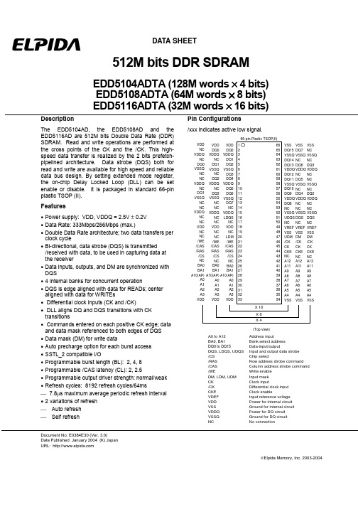
Pin Configurations
/xxx indicates active low signal.
66-pin Plastic TSOP(II) VDD VDD VDD NC DQ0 DQ0 VDDQ VDDQ VDDQ NC NC DQ1 DQ0 DQ1 DQ2 VSSQ VSSQ VSSQ NC NC DQ3 NC DQ2 DQ4 VDDQ VDDQ VDDQ NC NC DQ5 DQ1 DQ3 DQ6 VSSQ VSSQ VSSQ NC NC DQ7 NC NC NC VDDQ VDDQ VDDQ NC NC LDQS NC NC NC VDD VDD VDD NC NC NC NC NC LDM /WE /WE /WE /CAS /CAS /CAS /RAS /RAS /RAS /CS /CS /CS NC NC NC BA0 BA0 BA0 BA1 BA1 BA1 A10(AP) A10(AP) A10(AP) A0 A0 A0 A1 A1 A1 A2 A2 A2 A3 A3 A3 VDD VDD VDD 1 2 3 4 5 6 7 8 9 10 11 12 13 14 15 16 17 18 19 20 21 22 23 24 25 26 27 28 29 30 31 32 33 66 65 64 63 62 61 60 59 58 57 56 55 54 53 52 51 50 49 48 47 46 45 44 43 42 41 40 39 38 37 36 35 34 VSS VSS VSS DQ15 DQ7 NC VSSQ VSSQ VSSQ DQ14 NC NC DQ13 DQ6 DQ3 VDDQ VDDQ VDDQ DQ12 NC NC DQ11 DQ5 NC VSSQ VSSQ VSSQ DQ10 NC NC DQ9 DQ4 DQ2 VDDQ VDDQ VDDQ DQ8 NC NC NC NC NC VSSQ VSSQ VSSQ UDQS DQS DQS NC NC NC VREF VREF VREF VSS VSS VSS UDM DM DM /CK /CK /CK CK CK CK CKE CKE CKE NC NC NC A12 A12 A12 A11 A11 A11 A9 A9 A9 A8 A8 A8 A7 A7 A7 A6 A6 A6 A5 A5 A5 A4 A4 A4 VSS VSS VSS
中国印制电路行业排行榜暨PCB百强排行榜
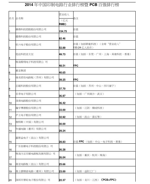
24
广州杰赛科技股份有限公司电子电 路分公司
5.95
25
上达电子(深圳)有限公司
5.80
26
深圳市精诚达电路科技股份有限公 司
5.78
FPC(包括:台[11、深圳)
27
深圳市新宇腾跃电子有限公司
5.74
FPC(原名:中兴新宇)
28
深圳市金百泽电州、西安、泽创、泽国、)
4
深圳市景旺电子股份有限公 司
22.37
(包括:龙川、江西)(PCB+FPC)
5
五株科技股份有限公司
20.33
(包括深圳、梅州、东莞)(PCB+FPC)
6
汕头超声印制板公司
19.52
7
深圳市兴森快捷电路科技股份有限 公司
16.74
8
深圳市崇达电路技术股份有限公 司
15.91
(包括:大连、江门)
9
广东兴达鸿业电子有限公司
32.92
(包括:昆山、黄石等)
13
奥特斯(中国)有限公司
30.00
14
华通电脑(惠州)有限公司
29.24
15
嘉联益电子(昆山)有限公司
28.83
估值FPC(包括:中山、电子科技、香港)
16
广东依顿电子科技股份有限公 司
26.28
17
珠海方正印刷电路板发展有限公 司
26.04
(包括:重庆、杭州、珠海)
江苏苏杭电子有限公司
7.54
18
厦门弘信电子科技股份有限公司
7.44
FPC
19
常州海弘/澳弘电子有限公司
6.69
20
吉安市满坤科技有限公司
电子技术及应用(刘刚)项目 (9)
项目四 直流稳压电源 图4-2-1 串联型稳压电源电路图
项目四 直流稳压电源 表4-2-2 串联型直流稳压电路测试数据
(三) 任务结论 根据测试与讨论的结果,写出实验研究报告(目的、原理 及方法、数据测试、分析及总结)。
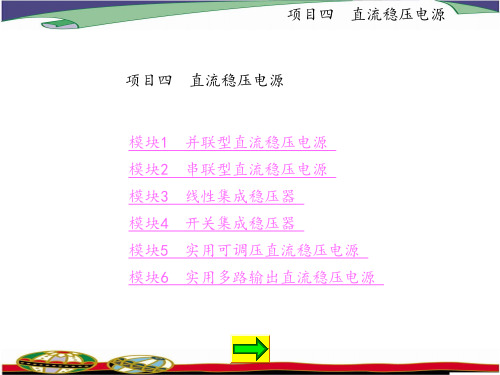
项目四 直流稳压电源
任务2 串联型稳压电源的测试 (一) 任务要求 (1) 串连型直流稳压电源的特点和性能指标的测试方法。 (2) 学会使用电子测量仪器进行电路的统调。 (3) 掌握直流稳压电源主要技术指标的测试方法(包括稳 压系数、输出电阻、最小输入电压、输出噪声电压等)。
根据表4-1-3,输入电压变化±10%,测量Udi、Udo的值, 并用示波器观察Udo的波形,均记入表4-1-3中。
(3) 改变负载电阻,观察稳压效果(U2=18 V保持不变); 根据表4-1-3测量Udi、Udo的值,记入表4-1-3中。
(4) 去掉图4-1-2所示电路中的滤波电容,用示波器同时 观察Udi、Udo的波形。
根据图4-2-1(b)所示的串联稳压电路,具体分析稳压电路 的稳压过程及输出电压的调节过程。
项目四 直流稳压电源
(三) 任务结论 根据测试与讨论的结果,写出实践研究报告(目的、原理 及方法、数据测试、分析及总结)。
项目四 直流稳压电源
【模块理论指导】 1. 模块基本要求 掌握 直流电源的整体电路分析。 理解 串联稳压电路的分析。 了解 直流电源相关参数的测试方法。 2. 模块重点和难点 重点 串联稳压电路分析,测试直流电源的性能参数。 难点 测试直流电源的性能参数。
项目四 直流稳压电源
学习问题: (1) 直流稳压电源由哪几部分组成?各组成部分的功能是 什么? (2) 整流电路有几种类型?各有什么特点?为什么一般采 用桥式整流? (3) 滤波电路的作用是什么?滤波电路有几种类型?各有 什么特点? (4) 论分析桥式整流电路输出电压与输入电压的关系以及 桥式整流加电容滤波电路输出电压与输入电压的关系,讨论整 流二极管的选择应考虑哪些因素。
电子电路设计任务书
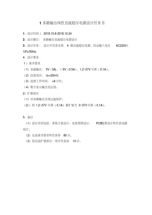
1多路输出线性直流稳压电源设计任务书1、设计时间: 2018.10.8-2018.10.242、设计题目:多路输出直流稳压电源设计3、设计任务:设计并仿真实现4路直流稳压电源。
给定输入电压AC220V±10%/50Hz。
4、设计要求1)基本要求(1)直流输出:5V(3A),±9V(0.5A),1.2~37V可调(0.1A);(2)纹波电压:U PP<20mV;(3)连续工作时间:>8小时;(4)数字显示输出电压值。
2)扩展部分(1)对各路输出实现过流保护;(2))将1.2~37V可调(0.1A)路扩展为0~37V可调(0.1A)。
5、备注(1)设计内容包括:系统方案设计、电原理图设计、PCB版图设计和仿真电路设计;(2)完成基本要求和仿真得80分;(3)每完成扩展部分一项并仿真加10分。
2开关型直流稳压电源设计任务书1、设计时间: 2018.10.8-2018.10.242、设计题目:开关型直流稳压电源3、设计任务:设计并仿真实现开关型直流稳压电源,输入交流电压AC220V ±10%(50~60Hz) 时,输出满足技术指标要求的直流电压,系统框图如下图所示。
开关稳压电源系统框图4.设计要求1) 基本要求(1)输出直流电压5V ,输出电流3A 。
(2)输入交流电压在180~250V 之间变化时,输出电压变化量小于2%。
(3)输出电阻R o <0.1。
(4)输出最大波纹电压<10mV 。
2) 发挥部分(1)具有过流保护功能。
(2)输出幅度数字显示功能。
5、备注(1)设计内容包括:系统方案设计、电原理图设计、PCB 版图设计和仿真电路设计;(2)完成基本要求和仿真得80分;(3)每完成扩展部分一项并仿真加10分。
译码显示A/D3车距报警器设计任务书1、设计时间: 2018.10.8-2018.10.242、设计题目:车距报警器设计3、设计任务:设计并仿真实现一个车距报警器,当探测到汽车之间小于一定距离时自动报警,系统框图如下图所示。
SPCA骏达电子1月、鑫鸿顺科技2月球叙圆满收杆

45PCB Information MAR 2019 NO.22019年1月18日,“SPCA 骏达电子2019年1月球叙”在东莞观澜的诺曼球场举行,本次球叙由骏达电子董事长徐欢赞助。
当天中午十二点,比赛正式开始。
PCB 行业健儿们各展身手。
经过几个小时的比赛,宏俐电子董事长张优胜荣膺冠军,深圳芽庄电子总经理苏军梅夺得亚军,威创新董事长王玉璋拿下季军。
2月28日,“SPCA 鑫鸿顺2月高尔夫球叙”在深圳艾斯球场举行。
SPCA 高尔夫球友们再次汇聚艾斯球场,逐鹿果岭!经过激烈角逐后,各项大奖也随之浮出水面,最终单佩武以80杆夺得总杆冠军,薛常耀以90冠获得总杆亚军,陈志文则以92杆获得总杆季军;净杆冠军为单佩武,总成绩74杆。
SPCA骏达电子1月、鑫鸿顺科技2月球叙圆满收杆2019年1~2月份,应企业邀请,GPCA/SPCA 常务副秘书长李帅一行参加松柏集团2018年度晚会、正业科技集团2019年迎春晚会、2019斯坦得&金盛科技合作签约暨联合春茗活动、2019东莞同昌电子迎春庆典等,与企业同乐,与行业共荣。
在过去的一年里,协会秉承共享、共融的理念,在省市各级政府部门的关心和指导下,在理事单位和会员单位积极参与和支持下,以“服务企业为第一要务”,GPCA/SPCA 的各项规划和活动得以稳步推进,会员数量持续增加,致力于发展成为有影响力、有活力的行业协会。
通过实地了解会员企业需求,协会积极协助企业开展各类项目如高新企业、技术改造、科技研发项目、节能减排补助、广东省著名商标、深圳市知名品牌等的申报工作,提升协会的桥梁、企业服务功能。
GPCA/SPCA参加多家PCB企业年会庆典2019年1月17日,由广东省印制电子电路产业技术创新联盟(GDPCIA)、GPCA/SPCA 联合举办的“2019 PCB 企业科研项目申报及技术研发人才培育交流论坛”在广州华工大学城中心酒店召开。
论坛由GDPCIA 秘书长暨GPCA 副秘书长陈世荣主持。
消防设计文件(峻凌电子(厦门)有限公司二期厂房二次装修工程))

消防设计文件项目名称:峻凌电子(厦门)有限公司二期厂房二次装修工程设计单位:钜匠装饰工程有限公司(盖章)日期: 2013年03月06日设计单位法定代表人:技术总负责人:项目总负责人:各专业负责人:目录1、设计说明书2、建筑平面图3、装修图纸4、电气图纸设计说明书一、工程设计依据:1、《建筑设计防火规范》GB50016-20062、《建筑内部装修设计防火规范》GB50222-953、《建筑装饰装修工程质量验收规范》GB50210-20014、《民用建筑电气设计规范》JGJ16-2008二、设计范围:峻凌电子(厦门)有限公司二期厂房二次装修工程,本次装修面积12005m2。
三、装修设计的功能及面积指标:一层:生产车间及办公室,面积5334m2,生产车间同时生产人数小于200人。
二层:生产车间及办公室,面积5436m2,生产车间同时生产人数小于200人。
三层:办公室,面积1235m2。
四、装修专业:主体耐火等级为二级主材概述:顶棚:轻钢龙骨12mm防火石膏板,顶棚燃烧等级A级。
墙面:室内隔断材料采用混凝土加气块、墙砖等。
地面:房间采用地砖(燃烧性能等级为A级)及PVC抗静电地板(燃烧性能等级为B1级);地面和其它部位为不低于B1级。
以上主材须符合相应防火等级五、电气专业1、本工程消防设备、应急照明及疏散指示按二级负荷进行设计,其余按三级负荷设计。
2、消防设备采用单独的供电回路,消防水泵、排烟风机等消防设备在最末一级配电箱处进行自动切换。
消防用电设备应设明显标志,其配电线路及供电回路按防火分区划分。
3、在车间、楼梯间、安全出口及走道设置应急照明及疏散指示。
4、应急灯和灯光疏散指示标志选择设有玻璃保护罩的灯具,消防应急照明和疏散指示标志采用蓄电池做备用电源,持续供电时间大于30min,并且火灾时有控制中心强制点亮。
5、消防电源干线采用ZBNYJV耐火交联聚氯乙烯电力电缆,应急照明线路采用阻燃铜芯导线ZRBV-450/750V穿KBG 管敷设,外刷防火涂料。
某地区某工业园厂房 (3)号车间电气cad设计施工图
开关电源过流保护电路设计方案分析

开关电源过流保护电路设计方案分析摘要:电子产品与我们的生活密不可分,大到国家项目建设,小到居民日常生活,在现代电子产品中,开关电源属于重要供电设备,从需求上来说要具备良好的性能,更为重要的是要注重其自身的保护措施。
为此,本文根据几种开关电源过流保护电路的设计方案进行分析,并简要介绍其工作原理。
关键词:开关电源;过流保护;电路;设计开关电源是日常生活中常见的电子产品,与我们的生活息息相关。
电源开关在日常实际工作过程中,由于输出的电源超出额定负载或者在电流短路时,就会造成系统故障使其无法正常运行。
针对这一生活中现象,为保证在发生故障后电源开关正常运行的安全性,就要求电路设计者对保护电路的问题进行合理设计。
一、利用浪涌电流,对电路进行限制浪涌电流的产生,主要是在对电源开关进行加电时引起的,过高的浪涌电流存在一定的危险性,因此要将其控制在合理范围内,就需要借助软启动装置,这种装置主要应用于电源输入端,通过它,能有效地防止浪涌电流的出现。
在对滤波电容充电时,极易产生浪涌电流,通过对开关管瞬时的导通,就极易导致较低的抗阻出现。
因此在实际的电路运行中,要采取必要的措施,控制浪涌电流的数值,防止其不断增加,甚至达到上百A的现象。
如图1所示,电容整流滤波电路是常见的开关电源输入方式,高、低频率的电容器常用在滤波电容C的选择上。
在并联容量较高频的电容器承担充放电电流的情况下,才可以选用低频率的电容器。
浪涌电流的冲击具有较大的危害性,为防止这一现象出现,就需要借助限流电阻RSC的力量,从图1中可以看到,串入在滤波与整流之间的部分就是RSC,通过RSC能让电容C的充电电流在合闸时受到限制。
通过短路使RSC完成启动的方式有两种:一种是当电容C1的电压经过一段时间的积累后到达继电器T动作电压的标准,另一种是滤波电容C的电压经过一段时间的累计后符合预设的数值时,这两种情况下都易使RSC完成启动。
图1整流滤波电路二、利用基极驱动电路,对电路进行限制通常来说,基极驱动电路的作用主要是用来分隔开关晶体管和控制电路的电源,将二者进行有效分离。
某工厂工程水电设计图(含设计说明书)

电子制造厂DFM材料
目录
4.6 阻焊层要求…………………………………………………..
4.7
4.8 Label Locations 5.0 PCB表面处理
5.1 PCB表面处理…………………………………………. 6.0 针对SMT的设计考虑……………………………………………
6.1 表面贴装技术指南…………………………………………… 6.2 SMT设计原则 6.3 SMT 零件高度考虑 6.4 基准 6.5 SMT 零件选择 7.0 焊盘设计…………………………………… 7.1 焊盘设计………………………………………………. 7.2 无源元件焊盘设计……………………………………..
脚间距为0.5mm或小于0.5mm都被认为是密间距元件 相邻的IC之间应有足够的空间以利于重工和目检 0.15 to 0.2英寸45
度 设计时使所有位于PCB 底面的元件尤其是翅型引脚包装的元件在同
一方向以利于波峰焊接。 所有的BGA通孔必须由阻焊层从上面盖住不必要的热转移 所有的元件位置应有清晰的标识,一直是元件是否放置 允许足够的测试接口以利于ICT测试
浸金制程是:“mono-molecular”即单 个分子厚度,因此制程不会超过 0.1um. 金在锡中完全溶解并与镍和锡生成合金,防止镍的氧化.无电 镀镍层的厚度 一般是3~5um.人们现在已经在关心金合金的脆性,金 的脆性问 题只有在பைடு நூலகம்的含量超过2~3wt.%或度层少于0.1um 是成立.
ENIG 虽昂贵,但是与其它表面处理相比镀金的含量是很低的
目录
8.5 Component Shadowing Considerations………………… 8.6 Via Hole Considerations…………………………………. 8.7 Lead Clinch ………………………………………………. 8.8 Seletive Wave Soldering Tutorial…………………………. 8.9 Selective Wave Soldering Design Considerations………… 8.10 UFO Hole…………………………………………………. 9.0 Design Consideration For Inspection And Repair……….. 9.1检查和维修指南 9.2检查和维修的设计规则 10.0 Design Consideration For Cleaning………………………… 10.1Design consideration for cleaning ………………….
模电资料库---2.3 印制电路板设计与制作
2.3 印制电路板设计与制作2.3.1印制电路板设计印刷电路板设计是电子设计制作中很关键的一步。
印制电路板的设计软件目前主要有Protel99、Orcad等。
1.设计步骤①设计好电路原理图;②根据所设计的原理图准备好所需要的元器件;③根据实物给原理图中的元器件制作或调用封装形式;④形成网络表连接文件;⑤在PCB设计环境下,规划电路板的大小、板层数量等;⑥调用网络表连接文件,并布局元器件的位置(自动加手工布局);⑦设置好自动布线规则,并自动布线;⑧形成第二个网络表连接文件,并比较两个网络表文件,若相同则说明没有问题,否则要查找原因;⑨手工布线并优化处理⑩输出PCB文件并制版。
2. 设计电路版时应该注意的问题①注意元器件的位置安排要满足散热的要求;②注意数字地和模拟地的分开;③当制作双面电路版时,由于是手工制作电路版,不可能进行过孔金属化,所以在制版时要尽量减少电路版层之间的过孔,并尽量用电阻、电容、三极管、二极管等实现过孔金属化工艺,但不能使用集成电路的引脚实现过孔金属化,换句话说是在设计电路板时,使用双列直插的集成电路时,与集成电路相联的覆铜线应全部放在电路板的底层。
④高阻抗、高灵敏度、低漂移的模拟电路、高速数字电路、高频电路的印制电路板设计需要专门的知识和技巧,需要参考有关资料。
其他有关印制电路板设计的问题可以参考有关资料。
2.3.2印制电路板的制作电路板的制作是电子设计竞赛设计的必不可少的环节。
本节介绍适合电子设计竞赛需要,使用Create-Pcb高精度电路板制作仪手工制作电路板过程,主要分为五个步骤:打印非林、曝光、显影、腐蚀和打空、双面连接及表面处理。
每个环节的都关系到制板的成功与否,因此制作过程中必须认真、仔细。
Create-SEM高精度电路板制作仪是美国Vplex公司最新研制出的高科技产品, 线径宽度最小可达4mil(0.1mm),是电子设计竞赛理想的印制板制作设备。
竞赛中,将PCB图送到电路板厂制作一般需要2~3天的时间,而且需要支付较高的制板费,而采用Create-SEM电路板制作仪仅只需一小时,低廉的费用,就可制作出一块高精度的单/双面板,特别是竞赛中当某电路板需要频繁修改试验时,Create-SEM电路板制作仪将以最低的成本,最快的速度满足您的需要。
YD-50开发设计表格
项目名称:YD-5 0油锯项目编号:OULIGEN-09-001
表号:
设计开发输入资料清单
编制:张德富日期:2009.03.05表号:QR21
设计开发评审报告
设计开发验证报告
表号:
设计开发输出资料清单
编制:张德富日期:2009.10.25表号:QR25
工艺验证报告
编制:张德富日期:表号:QR26
试产总结报告
功能实现程度:实现了市场的需求,提高了工作效率,达到了开发设计要求。
可靠性:经耐久试验,产品可靠性达到要求
批产工艺适应性:工艺安排合理,工人装配顺畅且质量有保证
材料批量供应可行性:零部件质量达到设计要求,大部分为市场通用型,通用性强。
备注:
编制:日期:
表号:QR27
试制申请单
制品名称:箱体试制时间:2009.08.05
配合部门及职责:配合部门:采购部;职责:按时按要求提供零件
资源需求:按照三维图一比一开模
配合部门及职责:配合部门:采购部;职责:按时按要求提供零件
资源需求:按三维图一比一
备注:
申请人:张德富日期:2009.08.05 审核:日期:
批准:日期:
表号:QR28
设计开发信息联络单
表号:QR28
设计开发信息联络单
发出信息:应新产品安装需要,请采购部尽快采购圆柱销5X 28
发出人:张德富日期:2009.10.02
回馈信息:
接收人:日期:。
- 1、下载文档前请自行甄别文档内容的完整性,平台不提供额外的编辑、内容补充、找答案等附加服务。
- 2、"仅部分预览"的文档,不可在线预览部分如存在完整性等问题,可反馈申请退款(可完整预览的文档不适用该条件!)。
- 3、如文档侵犯您的权益,请联系客服反馈,我们会尽快为您处理(人工客服工作时间:9:00-18:30)。
层数
成品板厚
压合结构
压合板厚
四层
0.6 MM
0.5OZ
1080
0.4
1080
0.5OZ
0.55mm
0.8 MM
0.5OZ
7628
0.4
7628
0.5OZ
0.75mm
四层
1.0 MM
0.5OZ
7628
0.6
7628
0.5OZ
0.95mm
1.2MM
0.5OZ
7628
0.8
7628
0.5OZ
C、工艺最易及成本最低。芯板越薄,处理工艺越难,成本增高;另外多张P片结构如内层基铜越厚(≥2OZ)须使用至少两张,肯定贵过单张P片结构等。Core Lamination结构的制作工艺肯定复杂过Foil Lamination结构,显然成本会较高;
D、埋孔、盲孔板的层压依据客户具体要求而定。
2.7内层压合厚度计算
0.15MM
±0.075MM
+0.15/-0.0MM
0.20MM
+0.0/-0.15MM
0.05MM
镀金
0.10MM
±0.075MM
+0.15/-0.0MM
0.15MM
+0.0/-0.15MM
不作补偿
+0.03/-0.02(PIN孔)
0.05MM(新钻咀)
NPTH hole
0.05MM
±0.05MM
A、除披锋孔加比相交位单边大0.10MM的孔。(两孔相交位较大)
B、钻完“1,2”两个孔后,除披锋孔在最后一把刀再钻一次“1”孔,(即钻孔顺序为“1,2,1)
1 2
3.14孔径≥5.0MM的大孔,需加3.0-4.0MM的预钻孔。
3.15邮票孔孔径一般为0.5-1.0MM(NPTH),孔边至孔边0.3-0.50MM。
料号孔依以上实际情况调节孔径大小,以便于区分。
4.内层干菲林
4.1内层菲林对位公差:±0.03MM,夹具公差±0.05mm。
4.2最小线宽、线距及补偿系数:
项目
感光线路
干膜
正常补偿
独立线补偿
最细线宽
最细线距
最细线宽
最细线距
H/H OZ底铜
0.1MM
0.1MM
0.1MM
0.1MM
0.02MM
0.04MM
B1、双面板:350X450MM(板厚0.4-1.0MM);
B2、双面板:420X600MM(板厚1.2-2.0MM);
C、多层板:350X450MM;
D、最小尺寸:150X200MM(样板开料);
E、电源板(完成3OZ)在开料利用率允许下,开料尽量控制在320X420MM范围内;
注意事项:(1)开料利用率及面积;
4.13多层板内层设计须在每层菲林的四角加做一个直径1.0mm的实心圆PAD,并在每个实心圆PAD的旁边注明该层的层数。层与层之间的PAD须错开约3mm且都不可重叠。实心圆PAD距角线距离≥3mm。
slot孔长宽比≥2倍时,钻径正常预大外还须将slot孔长度方向每边加长0.05MM(正常预大详见3.7)。
C、完成孔径公差:±0.076mm。
3.7钻孔补偿:
孔别
补偿
正常公差
特殊公差
补偿及要求
Via hole
+0至0.15MM
±0.075MM
钻咀尽量≥0.50MM
PTH hole
ENETK,喷锡,沉金
B、多层板内层尽量选用较厚材料,以减小半固化片的使用量;
C、当有两个以上的内层板需求时应尽量用相同板厚的内层,也可选用不同板厚的内层,但必须保证层压结构的对称;
D、内层铜厚应满足客户要求,如无要求则选用10Z铜作内层。
2.6层压结构图表示了多层板的构成,应考虑以下几点:
A、总厚度满足要求;
B、结构要严格对称(不对称的结构潜伏危险即易产生翘曲,特别是对SMT的多层板;
(不能超过30粒/PNL,且量大的不可以超过10粒/PNL否则改用干膜做或二钻钻出)。
3.12非金属化孔大于Φ1.5mm,如开模则用冲出(需加比孔少单边0.30MM的卸力孔,小于1.0MM的槽孔也需加卸力孔)。
3.13钻孔孔边与孔边≥0.20MM,小于0.2MM则考虑移孔或分刀钻出;孔径小于2.0MM,且两孔已相交,则需加比其钻咀小单边0.10MM的除披锋孔,具体按以下两种情况做:
A.出货单元(或SET)实际面积;
B.每Sheet的单元(或SET)数量;
C.所选用的Sheet面积。(Sheet是指一张大料)
1.6预留板边(成品有效外型到开料板边距离):
A、单/双面板:长边≥5.0MM;短边≥3.0MM;
B、多层板:长边≥12.0MM;短边≥8.0MM。
1.7烤板温度及时间:
A、CEM-1 130度3小时;
0.93mm
1.2MM
0.5OZ
2116
0.4
2116
0.4
2116
0.5OZ
1.12mm
1.6MM
0.5OZ
2116
0.6
2116
0.6
2116
0.5OZ
1.55mm
2.3以上内层压合的叠构是指在正常的层压需要下,无客户指定要求,无阻抗特殊要求的情况下的常规层压结构模式,八层以上层压结构另作核算。
+0.10/-0.0MM
0.10MM
+0.0/-0.10MM
不作补偿
注:一面线路为走线,另一面线路为独立PAD(两面电镀面积相差较大)的板,PTH孔钻咀预大0.2mm;slot孔预大0.2mm,但长度整体预大0.25mm。(此多为电源板)
3.8由于钻嘴直径的标称值尾数部分(小数点后第二位)只有5和0两种,所以钻嘴的加大值并不是固定不变的,而是有一个范围,具体情况见下表:(对于电源板可按最大范围加大,其他可以在此范围内选择。)
MIN HOLE SIZE
大赢数控
6.4mm
0.30mm
松林
6.4mm
0.30mm
最小钻咀0.30MM;最大钻咀6.40MM(以0.05MM递进)。
注:>φ6.4mm的孔,当无相应钻咀则采用扩孔方法。
3.2最大PANEL SIZE(单位:MM)
类型
松林
大赢数控
最小尺寸
单面
610×410
650×540
1.15mm
1.6MM
0.5OZ
7628
1.2
7628
0.5OZ
1.55mm
1.6MM
0.5OZ
1080
7628
1.0
7628
1080
0.5OZ
1.5mm
六层
0.8MM
0.5OZ
2116
0.2
2116
0.2
2116
0.5OZ
0.73mm
1.0MM
0.5OZ
2116
0.3
2116
0.3
2116
0.5OZ
1/1 OZ底铜
0.12MM
0.12MM
0.12MM
0.12MM
0.04MM
0.06MM
2/2 OZ底铜
0.20MM
0.20MM
0.20MM
0.20MM
0.08MM
0.10MM
4.3感光线路油板:板厚≥0.40MM。
4.4内层板边单边削铜:≥0.40MM,V-CUT≥0.50MM。
4.5内层隔离PAD要求每边比钻孔孔径≥0.25MM(一般≥0.30MM)。
3.16料号孔
A、各个数字从0-9用钻孔代表的定义:
0 1 2 3 4 5
6 7 8 9
注:以上孔与孔间距0.30MM以上,字与字孔间距为1.0MM以上。
B、各代号孔径要求:
(代表”1”用0.40-0.80MM的钻咀钻出)。
(代表”5”用1.0-1.30MM的钻咀钻出)
(代表”0”用1.6-2.5MM的钻咀钻出)。
注:A定位孔最佳≥3.0MM(即尽量考虑大的)。
B若作模具管位定位孔,不能用PTH孔定位,测试架定位孔可以用PTH或NPTH孔,但二钻孔不能用作定位孔
3.10 NPTH孔干膜最大封孔能力:圆孔4.0 mm; slot孔3.5X20MM
(干膜封孔单边保留≥0.20MM)。
3.11 NPTH孔塞胶粒最小孔径:1.50MM;最大孔径:4.50MM。
0.198±0.015
7628H
48.5±2%
0.216±0.013
7630
49.5±2%
0.229±0.020
7630HR
50.5
0.236±0.020
生益
1080
63±2%
0.076±0.010
2116
53±2%
0.117±0.010
7628
43±2%
0.191±0.013
7628H
50±2%
0.229±0.020
B、CEM-3 / FR-4 1245X1040MM、1245X1092MM(预定)。
1.2板厚:常用的一般由0.3mm到1.6mm各种规格。但不同厚度的完成厚度公差如下:
A、0.3-1.2MM完成板厚公差为+0.15/-0.05MM;
B、1.2MM以上完成板厚公差为板厚的+15%/-10%。
C、客户特殊要求除外。
B、CEM-3(黑板材)150度3小时/(白板材)130度2.5小时;
C、FR-4 150度4小时;150度6小时(双面无铅喷锡)
D、150度4小时(单面无铅喷锡)
2.多层板压合