RFP30P06中文资料
CommScope RFoG R-ONU 电源解决方案数据表说明书

DATA SHEET RF over Glass (RFoG)RFoG and RFPON ONU (R-ONU)Powering Solutions Most CommScope RFoG Optical Network Unit (R ‐ONU) devices require external power for operation. Separately sold powering solutions include compact low ‐cost high reliability wall ‐mounted AC ‐to ‐DC adapters with 12VDC or 15 VDC outputs and standard female "F" type connectors having nominal AC input voltages of 120 or 100 to 240 Volts AC. Input mains connectors fit NEMA ‐USA, EU, and UK style connectors common to various worldwide geographical regions. NEMA ‐USA mains plugs offer a wall plate mounting lug that ensures a secure installation. The required power supply depends on the R ‐ONU device being powered.A battery back ‐up Uninterruptible Power Supply (UPS) supporting 100 to 240 VAC input range is also available, for continuous operation during AC power failures. The PS1801B ‐00 battery for the PS1811U ‐01 UPS is sold separately. All power supplies feature “F” type female DC connectors for compatibility with the R ‐ONU connectors.•Designed for CommScope RFoG and RFPONR ‐ONU solutions•CSHMPIE high isolation 1.8 GHz power inserter•AC/DC wall adaptersPS1921W ‐10 SMPS with universal AC inputvoltage and connectors for NEMA ‐USA, EU,and UK applications. Meets international andUnited States DOE Class VI efficiencyspecificationPS1911W (120 VAC NEMA/US 1‐15P) (Maynot meet local efficiency regulations, thuslimiting use in certain countries.)All models above feature type “F” female DCoutput connectors•Uninterruptible Power SupplyUp to 20 hours of standard operation120 or 230 VAC inputType “F” female DC output connector•High reliability for long ‐term service FEATURESPS1921W ‐10PS1911PS1811U ‐01 UPSCSHMPIE PowerInserter (1.8GHz)PS1921W‐10: Universal AC voltage input range (100–240 VAC)•Multi‐country mains connector types•Meets International and USA Department of Energy (DOE) Class VI efficiency specifications•Connects directly to the R‐ONU, eliminating the PS1900‐ADP DC to F‐type adapter•Supports all CommScope CP8x R‐ONUs requiring external power suppliesPS1911W‐00: 120 VAC with USA NEMA 1‐15P AC connector and wall plate securing lugMay not meet local efficiency regulations, thus limiting use in certain countries. Operating temperature range may be less than that of the powered ONU.•Supports CommScope standard (non‐OBI‐free) R‐ONUsPS1811U‐01: Uninterruptable Power Supply (UPS)•Supports all CommScope CP8x R‐ONUsCSHMPIE Power InserterClass‐leading power inserter that provides maximum isolation between the power supply and the RF ports, preventing ingress when the R‐ONU is remotely powered via the RF coax. A Power Inserter is included with standard SDU and MDU non‐OBI‐freeR‐ONUs, not including the CP8600 models which have built‐in power supplies.SPECIFICATIONSPS1911W‐00 AC Wall Adapter120 V AC(nominal) USA type adapter with 12 V DC output on “F” connectorAC Input Voltage 108─132 V AC, 60 HzAC Input Connector NEMA 1‐15P (NP)DC Output Voltage12 V nominal @ 500 mADC Output Connector ANSI/SCTE 02:2006 type F FemaleSurge Protection1 kV min (per IEEE/ANSI C62.41)Safety UL 13210/CSA C22.2 No. 223‐M91Operating Temperature‐10°to +40°C (+14°to +104°F) NOTE: Operating range may be less than that of the powered ONU. Indoor mountingsuggested.Storage Temperature‐20°to +80°C (‐4°to +176°F)Humidity5% to 95% non‐condensingDimensions 2.3” W x 3.0” H x 2.0” D (5.8 cm x 7.6 cm x 5.0 cm)Weight, typ1 lb. (0.45 kg)Efficiency May not meet certain country regulations. Check local regulations before use.PS1921W‐10 Universal Power Supply Kit Wall mount AC/DC adapter provided with interchangeable AC adapter plates for US, EU, and UK applicationsAC Input Voltage100─240 V AC, 50/60 HzAC Input Connector Three interchangeable adapters: NEMA 1‐15P (NP), CEE 7/16 and BS1363 (USA, EU, and UK styles). USA adapterfeatures a mounting lug to secure adapter to the wall outlet.DC Output15 V DC@ 1.5 A maxDC Output Connector ANSI/SCTE 02.2006 compliant F‐type Coax ConnectorSurge Protection6 kV combination wave per IEEE/ANSI C62.41Operating Temperature‐10°to +40°C (14°to 104°F) @ 1.5 A max output current. NOTE: Operating range may be less than that of the poweredONU. Indoor mounting suggested.Storage Temperature‐40°to +85°C (‐40°to 185°F)Operating/Storage Humidity5% to 95% RH, non‐condensingDimensions 1.69" W x 3.35" H x 1.93" D (4.3 cm x 8.5 cm x 4.9 cm)Weight0.26 lb. (0.12 kg)EMC CE, BSMI, FCC, and VCCI compliantSafety IEC 60950‐1; EN 60950‐1; UL 60950‐1Efficiency Meets International and US DOE Class VI SpecificationsCSHMPIE Power InserterOperating Frequency5–1800 MHzInsertion loss RF to RF + Power1 dB maxReturn Loss20 dB (5 MHz to 1218 MHz)Isolation5–800 MHz 800–1218 MHz 1275–1800 MHz 75 dB min 70 dB min 65 dB minRF Shielding105 dB min per ANSI/SCTE 48‐2 2008 Operating Temperature‐40°to +65°C (‐40°to +149°F)Dimensions (L x W x H) 2.2 in x 1.57 in x 0.67 in (55.9 x 40.0 x 14.5 mm) Weight 1.0 oz (28 g) typRoHS Compliant YesPS1811U‐01 Uninterruptible Power Supply (UPS) Please review the individual data sheet for complete specifications.AC Input Voltage100–240 V RMS @ 0.5 A max, 50/60 HzInput Frequency50/60 HzAC Input Connector IEC 320/C6 inletPower Cord IEC 320/C5 to NEMA 5‐15Output Voltage12.0 V DC nominal (battery voltage upon loss of AC)Operational Output Power8 W maxOutput Connector ANSI/SCTE 02.2006 compliant F‐type Coax ConnectorDimensions 6.6” W x 7.75” H x 3.3” D (16.7 cm x 19.0 cm x 8.33 cm)Weight 1.2 lb (0.54 kg); battery: 5.7 lb (2.6 kg)Operating Temperature‐20°to +45°C (‐4°to 113°F) NOTE: Operating range may be less than that of the powered ONU. Indoor mountingsuggested.Storage Temperature‐20°to +45°C (‐4°to +113°F)Humidity5% to 95% non‐condensingSafety UL/CSA/EN 60950‐1EMC FCC Part 15 Class B, EN 55022, EN 55024Environmental CE Mark, RoHS compliantModel Identification Alpha FlexPoint FPR1208‐FPS1801B‐00 UPS Battery (Sold separately)12 V DC Standby Battery for PS1811U‐01 UPS7.2 AH AGM batteryProvides approximately 10 hours of backup at 6 W (or 20 hours at 3 W) to 25% reserve point shut‐off, based on new,fully‐charged batteryHot‐swappableRecharge time 18 hours to 90%Uses maintenance‐free sealed‐lead acidBattery Storage‐20°to +40°C (‐4°to 104°F), six months max storage duration at +25°C (+77°F) without a recharge SPECIFICATIONSRELATED PRODUCTSOR3144H, OR41x8H Diplexer/Receivers CH3000 Chassis and NH4000 VHub RFoG modulesXE4202M Remote OLT(R‐OLT)RFoG CP8xxx ONUsContact Customer Care for product information and sales:•United States: 866‐36‐ARRIS•International: +1‐678‐473‐5656Note: Specifications are subject to change without notice.Copyright Statement:©2022CommScope,Inc.All rights reserved.ARRIS and the ARRIS logo are trademarks of CommScope,Inc.and/or its affiliates.All other trademarks are the property of their respective owners.No part of this content may be reproduced in any form or by any means or used to make any derivative work(such as translation,transformation,or adaptation)without written permission from CommScope,Inc and/or its affiliates (“CommScope”).CommScope reserves the right to revise or change this content from time to time without obligation on the part of CommScope to provide notification of such revision or change.87‐10592‐RevN_RFoG‐and‐RFPON‐Powering‐Solutions。
6MBP30RH060中文资料
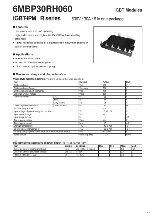
DC bus voltageDC bus voltage (Surge)DC bus voltage (Short operating)Collector-Emitter voltage Collector currentDC 1msDuty=56.6%Collector power dissipation One transistorJunction temperatureInput voltage of power supply for pre-driver Input signal voltage Input singal current Alarm signal voltage Alarm signal current Storage temperatureOperating case temperatureIsolating voltage (T erminal to base, 50/60Hz sine wave 1min.)Screw torque136MBP30RH060IGBT ModulesIGBT -IPM R series600V / 30A / 6 in one-packageq Absolute maximum ratings (Tc=25˚C unless otherwise specified)s Features• Low power loss and soft switching• High performance and high reliability IGBT with overheating protection• Higher reliability because of a big decrease in number of parts in built-in control circuits Applications• Inverter for motor drive• AC and DC servo drive amplifier • UPS (Uninterruptible power supply)s Maximum ratings and characteristicsItemSymbol Rating Unit V DCV DC (surge)V SC V CES I C I CP –I C P C T j V CC V in I in V ALM I ALM T stg T cop V isoMounting (M4)45050040060030603085150–0.3 to 20Vz 1Vcc 15–40 to 125–20 to 100AC 2500 2.0V V V V A A A W ˚C V V mA V mA ˚C ˚C V N • mq Electrical characteristics of power circuit (Tc=Tj=25˚C, Vcc=15V)Symbol I CESV CE (sat)V FConditionV CE =600V, Vin open Ic=30A –Ic=30AMin.–––Max.1.02.73.5Unit mA V VTyp.–––ItemCollector current at off signal input Collector-Emitter saturation voltage Forward voltage of FWD元器件交易网Min.0.5––Symbol t on t off t rrUnit µs µs µs14q Switching characteristics (Tc=Tj=25˚C, Vcc=15V)ItemConditionIc=30A, V DC =300V Inductive-LoadMax.–3.50.5Typ.–––Switching time (IGBT) See Fig. 3Switching time (FWD)Fig.1 Definition of OC delay timeFig.2 Definition of tscFig.3 Definition of switching timeDC bus voltageOperating power supply voltage range of pre-drive Switching frequency Flatness of heat sinkMounting screw torque (M4)Junction to case thermal resistanceCase to fin thermal resistance with compound ItemSymbol Rth (j-c)Rth (j-c)Rth (c-f)Max.1.472.1–Unit ˚C/W ˚C/W ˚C/WTyp.––0.05q Thermal characteristics (Tc=Tj=25˚C, Vcc=15V)IGBT FWDSymbol V DC V CC f sw ––ItemUnit V V kHz µm N • mTyp.–15–––Min. 200 13.5 1–100 1.3Max.40016.5201001.7q Recommendable valueMin.–––q Electrical characteristics of control circuit (Tc=Tj=25˚C, Vcc=15V)Shows theory dimensions15s Block diagrams Outline drawings, mmPre-driver 1 includes following functions. (P-side)• Amplifier for drive• Power supply undervoltage protection • IGBT chip overheating protectionPre-driver 2 includes following functions. (N-side)• Amplifier for drive• Power supply undervoltage protection • IGBT chip overheating protection • Overcurrent protection • Alarm signal outputMass : 50gs Characteristics (Representative)Collector current vs. Collector-emitter voltage Collector current vs. Collector-emitter voltage Switching losses vs. Collector current Switching losses vs. Collector currentSwitching time vs. Collector current Switching time vs. Collector current1617Forward voltage vs. Forward current Forward voltage vs. Forward currentTransient thermal resistance Power supply current vs. Switching frequencyOvercurrent protection vs. Case temperature。
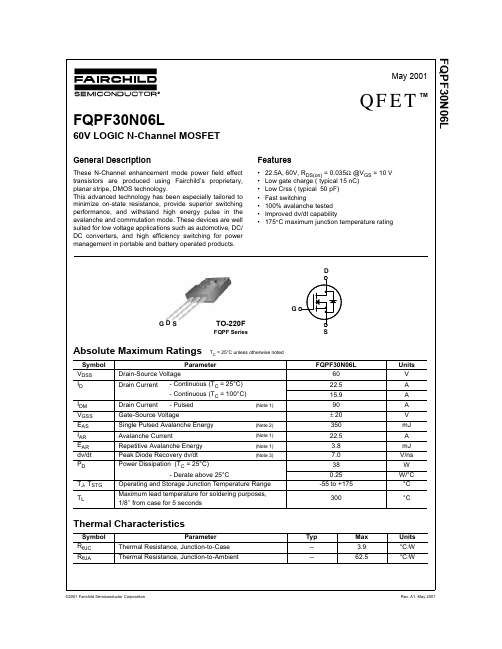
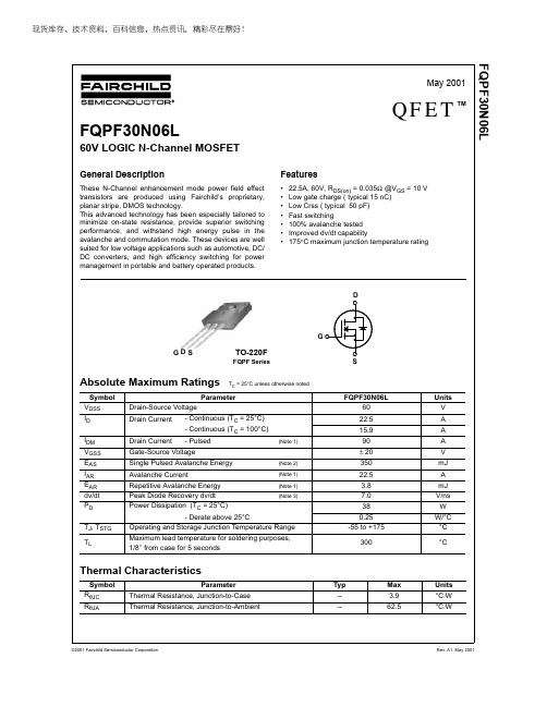
FQPF30N06L中文资料
Symbol
Parameter
TC = 25°C unless otherwise noted
Test Conditions
Min Typ Max Units
Off Characteristics
BVDSS ∆BVDSS / ∆TJ
Drain-Source Breakdown Voltage
Breakdown Voltage Temperature Coefficient
-- -100 nA
On Characteristics
VGS(th) Gate Threshold Voltage
RDS(on) Static Drain-Source On-Resistance
gFS
Forward Transconductance
VDS = VGS, ID = 250 µA
1.0 --
GD S
TO-220F
FQPF Series
D
!
"
!"
G!
" "
!
S
Absolute Maximum Ratings TC = 25°C unless otherwise noted
Symbol VDSS ID
IDM VGSS EAS IAR EAR dv/dt PD
TJ, TSTG
TL
Parameter
VGS = 0 V, ID = 250 µA
60
--
--
V
ID = 250 µA, Referenced to 25°C -- 0.06
--
V/°C
IDSS
Zero Gate Voltage Drain Current
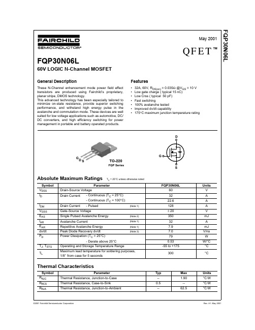
FQP30N06L中文资料
Min Typ Max Units
Off Characteristics
BVDSS ∆BVDSS / ∆TJ
Drain-Source Breakdown Voltage
Breakdown Voltage Temperature Coefficient
VGS = 0 V, ID = 250 µA
D
!
"
!"
G!
" "
!
S
FQP30N06L 60 32 22.6 128 ± 20 350 32 7.9 7.0 79 0.53
-55 to +175
300
Typ
Max
--
1.90
0.5
--
--
62.5
Units V A A A V mJ A mJ
V/ns W
W/°C °C
°C
Units °C/W °C/W °C/W
102
101
175℃
100
0.4
0.6
25℃
※ Notes :
1. VGS = 0V 2. 250μ s Pulse Test
0.8
1.0
1.2
1.4
1.6
VSD, Source-Drain voltage [V]
Figure 4. Body Diode Forward Voltage Variation vs. Source Current and Temperature
Figure 5. Capacitance Characteristics
Capacitance [pF]
©2001 Fairchild Semiconductor Corporation
HR30-6R-6P中文资料
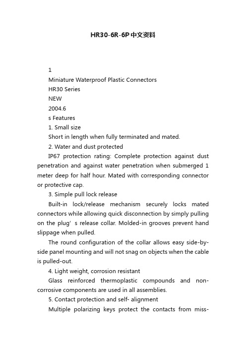
HR30-6R-6P中文资料1Miniature Waterproof Plastic ConnectorsHR30 SeriesNEW2004.6s Features1. Small sizeShort in length when fully terminated and mated.2. Water and dust protectedIP67 protection rating: Complete protection against dust penetration and against water penetration when submerged 1 meter deep for half hour. Mated with corresponding connector or protective cap.3. Simple pull lock releaseBuilt-in lock/release mechanism securely locks mated connectors while allowing quick disconnection by simply pulling on the plug’s release collar. Molded-in grooves prevent hand slippage when pulled.The round configuration of the collar allows easy side-by-side panel mounting and will not snag on objects when the cable is pulled-out.4. Light weight, corrosion resistantGlass reinforced thermoplastic compounds and non-corrosive components are used in all assemblies.5. Contact protection and self- alignmentMultiple polarizing keys protect the contacts from miss-alignment or attempted insertion of the wrong connector,while assuring correct mating between the corresponding connectors.6. Visual alignment indicatorsPermanent alignment indicators in a contrasting color on all connectors aid in correct alignment and engagement.7. Built-in cable strain relief s ApplicationsTest and measuring equipment, portable devices,instrumentation, industrial devices, recreational equipment,I/O applications and other applications requiring use of lightweight, corrosion resistant quick mate/ release cableconnections.Push-pull- single action lock15.542.112.632.33 and 6 pos.10 and 12 pos.Mated dimensionsLock/release operationPush-pull locking collar元器件交易网2s Product Specificationss Ordering informationHR 3 0 - 6 P A - 6 S C3s Plugsq Solder T ypeHR30-7P-12SC (Shown)Shown with terminated and installed contacts.Note: Crimp contacts are not included. Please order applicable contacts separately.HR30-6P-6S (Shown)4s Receptaclesq Solder TypeGasketBCADE(Thread)F(Hex nut)Lock washer12345HR30-6R-6P (Shown)q Through hole TypeHR30-8R-12SD (Shown)DCAB2Through hole post(0.2∞0.5)EF(Hex nut)GasketLock washerHR30-7R-12PC (Shown)Shown with terminated and installed contacts. Shown with terminated and installed contacts. Shown with terminated and installed contacts. Shown with terminated and installed contacts. Shown with terminated and installed contacts. Shown with terminated and installed contacts.5q Solder T ypeB(Fully tightened)A3456Applicablecable diameterHR30-7J-12PC (Shown)HR30-6J-6P (Shown)Shown with terminated and installed contacts.Note: Crimp contacts are not included. Please order applicable contacts separately.6q For Plugs11.4CABDEHR30-6R-CHR30-6P-CNote : When using these caps, do not use the gasket that is normally supplied with the receptacle. The “B” diameter end ofthe receptacle cap will serve as the gasket.7Note :Use wire size AWG 26 to 30 with a jacket diameter of 1 mm max.s Crimp ContactsB Connecting Combinations0.82111.151.2A-A cross-sectionAAPlugsHR30-*P-**Caps for Plug HR30-*P-CReceptacles HR30-*R-**JacksHR30-*J-**Caps for Receptacle HR30-*R-CCable(Shown for reference only.)CapCapPanel(Shown for reference only.)Male contactFemale contactNote 1 :When selecting connectors, take into account the shell size, contact count and gender of the contacts.Note 2 :When using the protective caps for the receptacles, do not use the gaskets normally supplied with the receptacle. Protective caps mustbe fully inserted to assure specified IP67 water and dust protection.8B Applicable Fixturesq Solder termination fixtureNote :The back shell tightening collar is used to tighten the back shell to the specified torque.Refer to assembly procedures.q Tightening collar for back shellSolder termination fixture Back shell tightening collar Note: The back shell tightening collar is used to tighten the back shell to specified torque.Refer to assembly procedures.HR30-6P-6S-T01HR30-6R-6P-T01HR30-6P-T029s Applicable ToolsNotes 1.The contact configuration depicts a view from the wiring side.2. Mounting to the panel is accomplished by tightening the hexagonal nut from the rear side of the panel.Manual contact crimping tool HT-102/HR30-1 Automatic contact crimping machine CM-105 Contact extraction tool HR30-TP10B Assembly Procedures1112B General usage notesB Precautions1. Do NOT apply force in excess of 30N in the directions shown below.2. To maintain the water/dust protection performance and the cable clamp force, use a cable that is within the range of applicable cable diameter.3. Consult HRS representative when using different cables.Panel30 N max.30 N max.30 N max.The contents of this catalog are current as of date of publication. Contents are subject to change without notice forthe purpose of improvements.5-23,OSAKI 5-CHOME,SHINAGAWA-KU,TOKYO 141-8587,JAPANPHONE: 81-3-3491-9741, FAX: 81-3-3493-2933。
BTRS-5940A-SPG中文资料

***********************************************************************************************************************************************************************OPTOWAY TECHNOLOGY INC. No .38, Kuang Fu S. Road, Hu Kou, Hsin Chu Industrial Park, Hsin Chu, Taiwan 303BTRS-5940G / BTRS-5940-SPG / BTRS-5940AG / BTRS-5940A-SPG1490 nm TX / 1310 nm RX , 3.3V / 155 Mbps RoHS Compliant Single-Fiber Transceiver*********************************************************************************************************************************************************************FEATURESl Single Fiber Bi-Directional Transceiver l 1490 nm DFB LD Transmitter l 1310 nm Receiver l Distance Up to 40 kml Single +3.3 V Power Supply l RoHS Compliantl LVPECL Differential Inputs and Outputs l 0 to 70o C Operating : BTRS-5940G l -20 to 85o C Operating : BTRS-5940AG l Wave Solderable and Aqueous Washablel Class 1 Laser International Safety Standard IEC-60825 CompliantAPPLICATIONSl WDM 622/155 Mb/s Linksl SONET/SDH Equipment Interconnect l Fiber Channel 532 Mb/s LinksDESCRIPTIONThe BTRS-5940G series is high performance module for single fiber communications by using 1490 nm transmitter and 1310 nm receiver. The transmitter section uses a multiple quantum well 1490 nm DFB laser and is a class 1 laser compliant according to International Safety Standard IEC-825. The receiver section uses an integrated 1310 nm detector preamplifier (IDP) mounted in an optical header and a limiting post-amplifier IC. A PECL logic interface simplifies interface to external circuitry.LASER SAFETYThis single mode transceiver is a Class 1 laser product. It complies with IEC 825 and FDA 21 CFR 1040.10 and 1040.11. The transceiver must be operated within the specified temperature and voltage limits. The optical ports of the module shall be terminated with an optical connector or with a dust plug.ORDER INFORMATIONP/No.Bit Rate (Mb/s) Distance (km) TX (nm) RX (nm) Voltage (V) Package Temp (o C)TX Power (dBm) RX Sens. (dBm) RoHS Compliant BTRS-5940G 622 40 1490 DFB 1310 3.3 2X5 SC 0 to 70 0 to -5 -28 Yes BTRS-5940AG622401490 DFB13103.32X5 SC -20 to 850 to -5-28YesNote: 1. BTRS-XXXXX: 2X5 SC receptacle type package. BTRL-XXXXX: 2X5 LC receptacle type package.2. BTRX-XXXXX-APBBB is 2X5 pigtail type package with different connector, A=S is SC connector, A=F is FC connector, A=T is ST connector, A=L is LC connector, A=M is MU connector; BBB is the length of fiber in cm.Absolute Maximum RatingsParameterSymbol Min Max Units NotesStorage Temperature Tstg -40 85 o COperating Temperature Topr 0 -20 70 85 o CBTRS-5940G BTRS-5940AGSoldering Temperature --- 260 oC 10 seconds on leads only Power Supply Voltage Vcc 0 4.5 V Input Voltage --- GND Vcc VOutput CurrentIout30mARecommended Operating ConditionsParameterSymbol Min Typ Max Units / NotesPower Supply Voltage Vcc 3.13 3.3 3.47 VOperating Temperature Topr 0 -20 70 85 oC / BTRS-5940G oC / BTRS-5940AGData Rate50 622 650 Mb/s Power Supply CurrentIcc260mATransmitter Specifications (0o C < Topr < 70o C, 3.13V < Vcc < 3. 47V)Parameter Symbol Min Typ Max Units NotesOpticalOptical Transmit Power Po -5 0 dBm 1Output Center Wavelength λ1480 1500 nmOutput Spectrum Width σλ 1 nm -20 dB Width Extinction Ratio E R10 dBOutput Eye Compliant with Bellcore TR-NWT-000253 and ITU recommendation G.957Optical Rise Time t r 1.2 ns 10% to 90% Values Optical Fall Time t f 1.2 ns 10% to 90% Values Relative Intensity Noise RIN -116 dB/HzTotal Jitter TJ 0.55 ns 2ElectricalData Input Current – Low I IL-350 µAData Input Current – High I IH350 µADifferential Input Voltage V IH - V IL300 1600 mVData Input Voltage – Low V IL - V CC-2.0 -1.58 V 3Data Input Voltage -- High V IH - V CC-1.1 -0.74 V 3Disable Input Voltage -- Low V TDIS,L0 0.8 V TX Output Enabled Disable Input Voltage -- High V TDIS,H Vcc – 1.3 Vcc V TX Ouput DisabledShut Off Time for TxDis t DIS 1 msNotes: 1. Output power is power coupled into a 9/125 µm single mode fiber.2. Measured with a 223-1 PRBS with 72 ones and 72 zeros.3. These inputs are compatible with 10K, 10KH and 100K ECL and LVPECL inputs.Receiver Specifications(0o C < Topr < 70o C, 3.13 V < Vcc < 3. 47V)Parameter Symbol Min Typ Max Units NotesOpticalSensitivity--- --- --- -28 dBm 1Maximum Input Power Pin -5 --- --- dBmSignal Detect -- Asserted Pa --- --- -28 dBm Transition: low to high Signal Detect -- Deasserted Pd -42 --- --- dBm Transition: high to low Signal detect -- Hysteresis 1.0 --- 4.0 dBWavelength of Operation 1260 1360 nm 2Optical Return Loss ORL 14 dBElectricalData Output Voltage – Low V OL - V CC-2.0 -1.58 V 3Data Output Voltage – High V OH - V CC-1.1 -0.74 V 3SD Output Voltage -- Low V OL - V CC-2.0 -1.58 V 3SD Output Voltage -- High V OH - V CC-1.1 -0.74 V 3Signal Detect Assert Time AS MAX100 µs OFF to ONSignal Detect Deassert Time ANS MAX300 µs ON to OFF Notes: 1. Minimum sensitivity and saturation levels at BER 1E-10 for a 223-1 PRBS with 72 ones and 72 zeros.2. At least 30 dB optical isolation for the wavelength 1480 to 1580 nm.3. These outputs are compatible with 10K, 10KH and 100K ECL and LVPECL outputs.********************************************************************************************************************************************************************* OPTOWAY TECHNOLOGY INC. No.38, Kuang Fu S. Road, Hu Kou, Hsin Chu Industrial Park, Hsin Chu, Taiwan 303 Tel: 886-3-5979798 Fax: 886-3-5979737********************************************************************************************************************************************************************* OPTOWAY TECHNOLOGY INC. No.38, Kuang Fu S. Road, Hu Kou, Hsin Chu Industrial Park, Hsin Chu, Taiwan 303 Tel: 886-3-5979798 Fax: 886-3-5979737RECOMMENDED CIRCUIT SCHEMATIC1)Recommended DC Coupled Interface Circuit2)Recommended AC Coupled Interface Circuit********************************************************************************************************************************************************************* OPTOWAY TECHNOLOGY INC. No.38, Kuang Fu S. Road, Hu Kou, Hsin Chu Industrial Park, Hsin Chu, Taiwan 303 Tel: 886-3-5979798 Fax: 886-3-5979737。
A3P060中文资料

ProASIC3 Devices
ARM-Enabled ProASIC3 Devices
A3P030 A3P060 A3P125
A3P250 3
A3P400 3
M7A3P250 3, 4 M7A3P400 3 I/O Type
A3P600 M7A3P600
A3P1000 M7A3P1000
Single-Ended I/O Single-Ended I/O Single-Ended I/O Single-Ended I/O2 Differential I/O Pairs Single-Ended I/O2 Differential I/O Pairs Single-Ended I/O2 Differential I/O Pairs Single-Ended I/O2 Differential I/O Pairs
M306NKFJGP中文资料
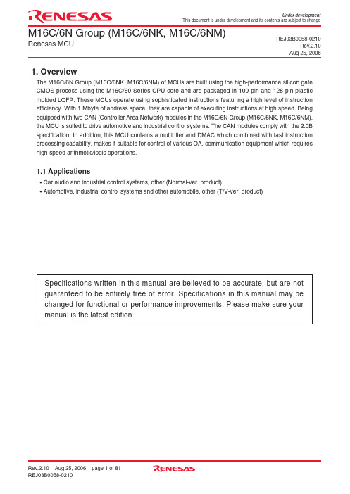
M16C/6N Group (M16C/6NK, M16C/6NM)Renesas MCUUnder developmentThis document is under development and its contents are subject to changeSpecifications written in this manual are believed to be accurate, but are not guaranteed to be entirely free of error. Specifications in this manual may be changed for functional or performance improvements. Please make sure your manual is the latest edition.REJ03B0058-0210Rev.2.10Aug 25, 20061. OverviewThe M16C/6N Group (M16C/6NK, M16C/6NM) of MCUs are built using the high-performance silicon gate CMOS process using the M16C/60 Series CPU core and are packaged in 100-pin and 128-pin plastic molded LQFP. These MCUs operate using sophisticated instructions featuring a high level of instruction efficiency. With 1 Mbyte of address space, they are capable of executing instructions at high speed. Being equipped with two CAN (Controller Area Network) modules in the M16C/6N Group (M16C/6NK, M16C/6NM),the MCU is suited to drive automotive and industrial control systems. The CAN modules comply with the 2.0B specification. In addition, this MCU contains a multiplier and DMAC which combined with fast instruction processing capability, makes it suitable for control of various OA, communication equipment which requires high-speed arithmetic/logic operations.1.1 Applications• Car audio and industrial control systems, other (Normal-ver. product)• Automotive, industrial control systems and other automobile, other (T/V-ver. product)元器件交易网ItemSpecificationNormal-ver.T/V-ver.CPU Number of fundamental 91 instructionsinstructionsMinimum instruction 41.7 ns (f(BCLK) = 24 MHz,50.0 ns (f(BCLK) = 20 MHz,execution time 1/1 prescaler, without software wait)1/1 prescaler, without software wait)Operating mode Single-chip, memory expansion, Single-chip modeand microprocessor modesAddress space 1 Mbyte Memory capacity Refer to Table 1.3 Product InformationPeripheral Ports Input/Output: 87 pins, Input: 1 pin Function Multifunction timers Timer A: 16 bits ✕ 5 channelsTimer B: 16 bits ✕ 6 channels Three-phase motor control circuitSerial interfaces 3 channelsClock synchronous, UART, I 2C-bus (1), IEBus (2)2 channelsClock synchronousA/D converter 10-bit A/D converter: 1 circuit, 26 channels D/A converter 8 bits ✕ 2 channels DMAC 2 channels CRC calculation circuit CRC-CCITT CAN module 2 channels with 2.0B specification Watchdog timer 15 bits ✕ 1 channel (with prescaler)Interrupts Internal: 32 sources, External: 9 sourcesSoftware: 4 sources, Priority levels: 7 levelsClock generation circuits 4 circuits• Main clock oscillation circuit (*)• Sub clock oscillation circuit (*)• On-chip oscillator• PLL frequency synthesizer(*) Equipped with on-chip feedback resistorOscillation-stopped detector Main clock oscillation stop and re-oscillation detection functionElectrical Supply voltage VCC = 3.0 to 5.5 V (f(BCLK) = 24 MHz,VCC = 4.2 to 5.5 V (f(BCLK) = 20 MHz,Characteristics 1/1 prescaler, without software wait)1/1 prescaler, without software wait)Consumption Mask ROM 21 mA (f(BCLK) = 24 MHz,-current PLL operation, no division)Flash memory 23 mA (f(BCLK) = 24 MHz,21 mA (f(BCLK) = 20 MHz,PLL operation, no division)PLL operation, no division)Mask ROM 3 µA (f(BCLK) = 32 kHz, Wait mode, Oscillation capacity Low)Flash memory 0.8 µA (Stop mode, Topr = 25°C)Flash Memory Programming and erasure voltage 3.0 ± 0.3 V or 5.0 ± 0.5 V 5.0 ± 0.5 V Version Programming and erasure endurance 100 times I/O I/O withstand voltage 5.0 V Characteristics Output current 5 mA Operating Ambient Temperature -40 to 85°C T version: -40 to 85°CV version: -40 to 125°C (option)Device Configuration CMOS high-performance silicon gate Package 100-pin molded-plastic LQFP 1.2 Performance OverviewTables 1.1 and 1.2 list the Functions and Specifications for M16C/6N Group (M16C/6NK, M16C/6NM).Table 1.1 Functions and Specifications for M16C/6N Group (100-pin Version: M16C/6NK)NOTES:1. I 2C-bus is a trademark of Koninklijke Philips Electronics N.V.2. IEBus is a trademark of NEC Electronics Corporation.option: All options are on request basis.ItemSpecificationNormal-ver.T/V-ver.CPU Number of fundamental91 instructionsinstructionsMinimum instruction41.7 ns (f(BCLK) = 24 MHz,50.0 ns (f(BCLK) = 20 MHz,execution time1/1 prescaler, without software wait)1/1 prescaler, without software wait)Operating mode Single-chip, memory expansion, Single-chip modeand microprocessor modesAddress space 1 MbyteMemory capacity Refer to Table 1.3 Product InformationPeripheral Ports Input/Output: 113 pins, Input: 1 pinFunction Multifunction timers Timer A: 16 bits ✕ 5 channelsTimer B: 16 bits ✕ 6 channelsThree-phase motor control circuitSerial interfaces 3 channelsClock synchronous, UART, I2C-bus (1), IEBus (2)4 channelsClock synchronousA/D converter10-bit A/D converter: 1 circuit, 26 channelsD/A converter8 bits ✕ 2 channelsDMAC 2 channelsCRC calculation circuit CRC-CCITTCAN module 2 channels with 2.0B specificationWatchdog timer15 bits ✕ 1 channel (with prescaler)Interrupts Internal: 34 sources, External: 12 sourcesSoftware: 4 sources, Priority levels: 7 levelsClock generation circuits 4 circuits• Main clock oscillation circuit (*)• Sub clock oscillation circuit (*)• On-chip oscillator• PLL frequency synthesizer(*) Equipped with on-chip feedback resistorOscillation-stopped detector Main clock oscillation stop and re-oscillation detection function Electrical Supply voltage VCC = 3.0 to 5.5 V (f(BCLK) = 24 MHz,VCC = 4.2 to 5.5 V (f(BCLK) = 20 MHz, Characteristics1/1 prescaler, without software wait)1/1 prescaler, without software wait) Consumption Mask ROM21 mA (f(BCLK) = 24 MHz,-current PLL operation, no division)Flash memory23 mA (f(BCLK) = 24 MHz,21 mA (f(BCLK) = 20 MHz,PLL operation, no division)PLL operation, no division)Mask ROM 3 µA (f(BCLK) = 32 kHz, Wait mode, Oscillation capacity Low)Flash memory0.8 µA (Stop mode, Topr = 25°C)Flash Memory Programming and erasure voltage 3.0 ± 0.3 V or 5.0 ± 0.5 V 5.0 ± 0.5 VVersion Programming and erasure endurance100 timesI/O I/O withstand voltage 5.0 VCharacteristics Output current 5 mAOperating Ambient Temperature-40 to 85°C T version: -40 to 85°CV version: -40 to 125°C (option) Device Configuration CMOS high-performance silicon gatePackage128-pin molded-plastic LQFPTable 1.2 Functions and Specifications for M16C/6N Group (128-pin Version: M16C/6NM)NOTES:1. I2C-bus is a trademark of Koninklijke Philips Electronics N.V.2. IEBus is a trademark of NEC Electronics Corporation.option: All options are on request basis.1.4 Product InformationTable 1.3 lists the Product Information and Figure 1.2 shows the Type Number, Memory Size, and Packages.Table 1.3 Product Information As of Aug. 2006 Type No.ROM Capacity RAM Capacity Package Type (2)RemarksM306NKFHGP384 K + 4 Kbytes31 Kbytes PLQP0100KB-A Flash Normal-ver. M306NMFHGP PLQP0128KB-A memoryM306NKFJGP512 K + 4 Kbytes31 Kbytes PLQP0100KB-A version (1)M306NMFJGP PLQP0128KB-AM306NKFHTGP(D)384 K + 4 Kbytes31 Kbytes PLQP0100KB-A T-ver.M306NMFHTGP(D)PLQP0128KB-AM306NKFJTGP512 K + 4 Kbytes31 Kbytes PLQP0100KB-AM306NMFJTGP PLQP0128KB-AM306NKFHVGP(D)384 K + 4 Kbytes31 Kbytes PLQP0100KB-A V-ver.M306NMFHVGP(D)PLQP0128KB-AM306NKFJVGP(D)512 K + 4 Kbytes31 Kbytes PLQP0100KB-AM306NMFJVGP(D)PLQP0128KB-AM306NKME-XXXGP192 Kbytes16 Kbytes PLQP0100KB-A Mask Normal-ver. M306NMME-XXXGP PLQP0128KB-A ROMM306NKMG-XXXGP256 Kbytes20 Kbytes PLQP0100KB-A versionM306NMMG-XXXGP PLQP0128KB-A(D): Under developmentNOTES:1. Data flash memory provides an additional 4 Kbytes of ROM capacity (block A).2. The correspondence between new and old package types is as follows.PLQP0100KB-A: 100P6Q-APLQP0128KB-A: 128P6Q-AType No. M30 6N K M G T - XXX GPPackage type:GP: Package PLQP0100KB-A (100P6Q-A)PLQP0128KB-A (128P6Q-A)ROM No.Omitted on flash memory versionCharacteristics(no): Normal-ver.T: T-ver. (Automotive 85°C version)V: V-ver.(Automotive 125°C version)ROM capacity:E: 192 KbytesG: 256 KbytesH: 384 KbytesJ: 512 KbytesMemory type:M: Mask ROM versionF: Flash memory versionShows the number of CAN module, pin count, etc.6N GroupM16C FamilyFigure 1.2 Type Number, Memory Size, and PackagePin No.ControlPortInterruptTimer Pin UART PinAnalog CAN Module Bus Control Pin Pin Pin Pin Pin (1)1P9_4TB4IN DA12P9_3TB3IN DA03P9_2TB2IN SOUT34P9_1TB1IN SIN35P9_0TB0IN CLK36BYTE7CNVSS8XCIN P8_79XCOUT P8_610_____________RESET11XOUT12VSS13XIN14VCC115P8_5________NMI16P8_4_________INT2ZP17P8_3_________INT118P8_2_________INT019P8_1___TA4IN/U20P8_0TA4OUT/U(SIN4)21P7_7TA3IN CRX122P7_6TA3OUT CTX123P7_5____TA2IN/W(SOUT4)24P7_4TA2OUT/W(CLK4)25P7_3___TA1IN/V____________________CTS2/RTS226P7_2TA1OUT/V CLK227P7_1TA0IN/TB5IN RXD2/SCL228P7_0TA0OUT TXD2/SDA229P6_7TXD1/SDA130P6_6RXD1/SCL131P6_5CLK132P6_4___________________________CTS1/RTS1/CTS0/CLKS133P6_3TXD0/SDA034P6_2RXD0/SCL035P6_1CLK036P6_0____________________CTS0/RTS037P5_7_________RDY/CLKOUT 38P5_6ALE39P5_5___________HOLD 40P5_4___________HLDA 41P5_3BCLK42P5_2______RD 43P5_1__________________WRH/BHE 44P5_0_______________WRL/WR 45P4_7_______CS3 46P4_6_______CS2 47P4_5_______CS1 48P4_4_______CS0 49P4_3A1950P4_2A18 NOTE:1. Not available the bus control pins (except CLKOUT pin; Pin No.37) in T/V-ver..Pin No.ControlPortInterruptTimer Pin UART PinAnalog CAN Module Bus Control Pin Pin Pin Pin Pin (1)51P4_1A17 52P4_0A16 53P3_7A15 54P3_6A14 55P3_5A13 56P3_4A12 57P3_3A11 58P3_2A10 59P3_1A960VCC261P3_0A8(/-/D7) 62VSS63P2_7AN2_7A7(/D7/D6) 64P2_6AN2_6A6(/D6/D5) 65P2_5AN2_5A5(/D5/D4) 66P2_4AN2_4A4(/D4/D3) 67P2_3AN2_3A3(/D3/D2) 68P2_2AN2_2A2(/D2/D1) 69P2_1AN2_1A1(/D1/D0) 70P2_0AN2_0A0(/D0/-) 71P1_7_________INT5D15 72P1_6_________INT4D14 73P1_5_________INT3D13 74P1_4D12 75P1_3D11 76P1_2D10 77P1_1D978P1_0D879P0_7AN0_7D780P0_6AN0_6D681P0_5AN0_5D582P0_4AN0_4D483P0_3AN0_3D384P0_2AN0_2D285P0_1AN0_1D186P0_0AN0_0D087P10_7______KI3AN788P10_6______KI2AN689P10_5______KI1AN590P10_4______KI0AN491P10_3AN392P10_2AN293P10_1AN194AVSS95P10_0AN096VREF97AVCC98P9_7SIN4______________ADTRG 99P9_6SOUT4ANEX1CTX0100P9_5CLK4ANEX0CRX0NOTE:1. Not available the bus control pins in T/V-ver..Table 1.6 List of Pin Names for 128-Pin Package (1)Pin No.ControlPortInterruptTimer Pin UART PinAnalog CAN Module Bus Control Pin Pin Pin Pin Pin (1)1VREF2AVCC3P9_7SIN4______________ADTRG4P9_6SOUT4ANEX1CTX05P9_5CLK4ANEX0CRX06P9_4TB4IN DA17P9_3TB3IN DA08P9_2TB2IN SOUT39P9_1TB1IN SIN310P9_0TB0IN CLK311P14_112P14_013BYTE14CNVSS15XCIN P8_716XCOUT P8_617_____________RESET18XOUT19VSS20XIN21VCC122P8_5________NMI23P8_4_________INT2ZP24P8_3_________INT125P8_2_________INT026P8_1___TA4IN/U27P8_0TA4OUT/U(SIN4)28P7_7TA3IN CRX129P7_6TA3OUT CTX130P7_5____TA2IN/W(SOUT4)31P7_4TA2OUT/W(CLK4)32P7_3___TA1IN/V____________________CTS2/RTS233P7_2TA1OUT/V CLK234P7_1TA0IN/TB5IN RXD2/SCL235P7_0TA0OUT TXD2/SDA236P6_7TXD1/SDA137VCC138P6_6RXD1/SCL139VSS40P6_5CLK141P6_4___________________________CTS1/RTS1/CTS0/CLKS142P6_3TXD0/SDA043P6_2RXD0/SCL044P6_1CLK045P6_0____________________CTS0/RTS046P13_7_________INT847P13_6_________INT748P13_5_________INT649P13_450P5_7_________RDY/CLKOUT NOTE:1. Not available the bus control pins (except CLKOUT pin; Pin No.50) in T/V-ver..Pin No.ControlPortInterruptTimer Pin UART PinAnalog CAN Module Bus Control Pin Pin Pin Pin Pin (1)51P5_6ALE 52P5_5___________HOLD 53P5_4___________HLDA 54P13_355P13_256P13_157P13_058P5_3BCLK 59P5_2______RD 60P5_1__________________WRH/BHE 61P5_0_______________WRL/WR 62P12_763P12_664P12_565P4_7_______CS3 66P4_6_______CS2 67P4_5_______CS1 68P4_4_______CS0 69P4_3A19 70P4_2A18 71P4_1A17 72P4_0A16 73P3_7A15 74P3_6A14 75P3_5A13 76P3_4A12 77P3_3A11 78P3_2A10 79P3_1A980P12_481P12_382P12_283P12_184P12_085VCC286P3_0A8(/-/D7) 87VSS88P2_7AN2_7A7(/D7/D6) 89P2_6AN2_6A6(/D6/D5) 90P2_5AN2_5A5(/D5/D4) 91P2_4AN2_4A4(/D4/D3) 92P2_3AN2_3A3(/D3/D2) 93P2_2AN2_2A2(/D2/D1) 94P2_1AN2_1A1(/D1/D0) 95P2_0AN2_0A0(/D0/-) 96P1_7_________INT5D15 97P1_6_________INT4D14 98P1_5_________INT3D13 99P1_4D12 100P1_3D11 NOTE:Pin No.ControlPortInterruptTimer Pin UART PinAnalog CAN Module Bus Control Pin Pin Pin Pin Pin (1)101P1_2D10 102P1_1D9 103P1_0D8 104P0_7AN0_7D7 105P0_6AN0_6D6 106P0_5AN0_5D5 107P0_4AN0_4D4 108P0_3AN0_3D3 109P0_2AN0_2D2 110P0_1AN0_1D1 111P0_0AN0_0D0 112P11_7SIN6113P11_6SOUT6114P11_5CLK6115P11_4116P11_3117P11_2SOUT5118P11_1SIN5119P11_0CLK5120P10_7______KI3AN7 121P10_6______KI2AN6 122P10_5______KI1AN5 123P10_4______KI0AN4 124P10_3AN3125P10_2AN2126P10_1AN1127AVSS128P10_0AN0NOTE:1. Not available the bus control pins in T/V-ver..1.6 Pin FunctionsTables 1.9 to 1.11 list the Pin Functions.Table 1.9 Pin Functions (100-pin and 128-pin Versions) (1)I I I III/O I/O O I/OI/OO OO I O IVCC1, VCC2,VSSAVCC, AVSS_____________RESET CNVSSBYTE D0 to D7D8 to D15A0 to A19A0/D0 to A7/D7A1/D0 to A8/D7______________CS0 to CS3_______________WRL/WR _________________WRH/BHE ______RDALE __________HOLD__________HLDA ________RDYPower supply inputAnalog power supply input Reset input CNVSS (2)External data bus widthselect input (2)Bus control pins (3)Apply 3.0 to 5.5 V to the VCC1 and VCC2 pins and 0 V to the VSSpin. The VCC apply condition is that VCC2 = VCC1 (1).Applies the power supply for the A/D converter. Connect the AVCC pin to VCC1. Connect the AVSS pin to VSS.The MCU is in a reset state when applying “L ” to the this pin.Switches processor mode. Connect this pin to VSS to when after a reset to start up in single-chip mode. Connect this pin to VCC1to start up in microprocessor mode.Switches the data bus in external memory space. The data bus is 16-bit long when the this pin is held “L ” and 8-bit long when the this pin is held “H ”. Set it to either one. Connect this pin to VSS when single-chip mode.Inputs and outputs data (D0 to D7) when these pins are set as the separate bus.Inputs and outputs data (D8 to D15) when external 16-bit data bus is set as the separate bus.Output address bits (A0 to A19).Input and output data (D0 to D7) and output address bits (A0 to A7) by time-sharing when external 8-bit data bus are set as the multiplexed bus.Input and output data (D0 to D7) and output address bits (A1 to A8) by time-sharing when external 16-bit data bus are set as the multiplexed bus.____________________________Output CS0 to CS3 signals. CS0 to CS3 are chip-select signals to specify an external space._____________________________________________________Output WRL, WRH, (WR, BHE), RD signals. WRL and WRH or ______________BHE, and WR can be switched by program.______________________• WRL, WRH, and RD are selected ________The WRL signal becomes “L ” by writing data to an even address in an external memory space._________The WRH signal becomes “L ” by writing data to an odd address in an external memory space._____The RD pin signal becomes “L ” by reading data in an external memory space.___________________• WR, BHE, and RD are selected ______The WR signal becomes “L ” by writing data in an external memory space._____The RD signal becomes “L ” by reading data in an external memory space.________The BHE signal becomes “L ” by accessing an odd address.___________________Select WR, BHE, and RD for an external 8-bit data bus.ALE is a signal to latch the address.__________While the HOLD pin is held “L ”, the MCU is placed in a hold state.__________In a hold state, HLDA outputs a “L ” signal.________While applying a “L ” signal to the RDY pin, the MCU is placed in a wait state.Signal NamePin Name I/O Type DescriptionI: Input O: Output I/O: Input/OutputNOTES:1. In this manual, hereafter, VCC refers to VCC1 unless otherwise noted.2. Connect to VSS in T/V-ver..I O I O O O I I I I/O I I I O I O I/O I I O O O I/O I/O I II I/OI OI OXIN XOUT XCIN XCOUT BCLK CLKOUTNT0 to INT8 (2)________NMI____________KI0 to KI3TA0OUT to TA4OUT TA0IN to TA4IN ZPTB0IN to TB5IN __________U, U, V, V, W, W ____________________CTS0 to CTS2____________________RTS0 to RTS2CLK0 to CLK6 (2)RXD0 to RXD2SIN3 to SIN6 (2)TXD0 to TXD2SOUT3 to SOUT6 (2)CLKS1SDA0 to SDA2SCL0 to SCL2VREFAN0 to AN7AN0_0 to AN0_7AN2_0 to AN2_7_____________ADTRG ANEX0ANEX1DA0, DA1CRX0, CRX1CTX0, CTX1Main clockinputMain clock output Sub clock inputSub clock outputBCLK output (3)Clock output INT interrupt input _______NMI interrupt inputKey inputinterrupt input Timer ATimer B Three-phase motor control output Serial interface I 2C modeReference voltage input A/D converterD/A converter CAN module I/O pins for the main clock oscillation circuit. Connect a ceramicresonator or crystal oscillator between XIN and XOUT (1).To use the external clock, input the clock from XIN and leave XOUT open.I/O pins for a sub clock oscillation circuit. Connect a crystal oscillator between XCIN and XCOUT (1).To use the external clock, input the clock from XCIN and leave XCOUT open.Outputs the BCLK signal.The clock of the same cycle as fC, f8, or f32 is output.______Input pins for the INT interrupt._______Input pin for the NMI interrupt.Input pins for the key input interrupt.These are timer A0 to timer A4 I/O pins.These are timer A0 to timer A4 input pins.Input pin for the Z-phase.These are timer B0 to timer B5 input pins.These are Three-phase motor control output pins.These are transmit control input pins.These are receive control output pins.These are transfer clock I/O pins.These are serial data input pins.These are serial data input pins.These are serial data output pins.These are serial data output pins.This is output pin for transfer clock output from multiple pins function.These are serial data I/O pins.These are transfer clock I/O pins. (however, SCL2 for the N-channel open drain output.)Applies the reference voltage for the A/D converter and D/A converter.Analog input pins for the A/D converter.This is an A/D trigger input pin.This is the extended analog input pin for the A/D converter,and is the output in external op-amp connection mode.This is the extended analog input pin for the A/D converter.These are the output pins for the D/A converter.These are the input pins for the CAN module.These are the output pins for the CAN module.Signal Name Pin Name I/O TypeDescriptionI: Input O: Output I/O: Input/OutputNOTES:1. Ask the oscillator maker the oscillation characteristic.________________2. INT6 to INT8, CLK5, CLK6, SIN5, SIN6, SOUT5, SOUT6 are only in the 128-pin version.8-bit I/O ports in CMOS, having a direction register to select an input or output.Each pin is set as an input port or output port. An input port can be set for a pull-up or for no pull-up in 4-bit unit by program.(however P7_1 and P9_1 for the N-channel open drain output.)_______Input pin for the NMI interrupt.Pin states can be read by the P8_5 bit in the P8 register.I/O portInput portP0_0 to P0_7P1_0 to P1_7P2_0 to P2_7P3_0 to P3_7P4_0 to P4_7P5_0 to P5_7P6_0 to P6_7P7_0 to P7_7P8_0 to P8_4P8_6, P8_7P9_0 to P9_7P10_0 to P10_7P11_0 to P11_7 (1)P12_0 to P12_7 (1)P13_0 to P13_7 (1)P14_0, P14_1 (1)P8_5I/OISignal NamePin Name I/O Type DescriptionI: Input O: Output I/O: Input/Output NOTE:1. Ports P11 to P14 are only in the 128-pin version.2.3 Frame Base Register (FB)FB is configured with 16 bits, and is used for FB relative addressing.2.4 Interrupt Table Register (INTB)INTB is configured with 20 bits, indicating the start address of an interrupt vector table.2.5 Program Counter (PC)PC is configured with 20 bits, indicating the address of an instruction to be executed.2.6 User Stack Pointer (USP), Interrupt Stack Pointer (ISP)Stack pointer (SP) comes in two types: USP and ISP, each configured with 16 bits.Your desired type of stack pointer (USP or ISP) can be selected by the U flag of FLG.2.7 Static Base Register (SB)SB is configured with 16 bits, and is used for SB relative addressing.2.8 Flag Register (FLG)FLG consists of 11 bits, indicating the CPU status.2.8.1 Carry Flag (C Flag)This flag retains a carry, borrow, or shift-out bit that has occurred in the arithmetic/logic unit.2.8.2 Debug Flag (D Flag)This flag is used exclusively for debugging purpose. During normal use, set to 0.2.8.3 Zero Flag (Z Flag)This flag is set to 1 when an arithmetic operation resulted in 0; otherwise, it is 0.2.8.4 Sign Flag (S Flag)This flag is set to 1 when an arithmetic operation resulted in a negative value; otherwise, it is 0.2.8.5 Register Bank Select Flag (B Flag)Register bank 0 is selected when this flag is 0; register bank 1 is selected when this flag is 1.2.8.6 Overflow Flag (O Flag)This flag is set to 1 when the operation resulted in an overflow; otherwise, it is 0.2.8.7 Interrupt Enable Flag (I Flag)This flag enables a maskable interrupt.Maskable interrupts are disabled when the I flag is 0, and are enabled when the I flag is 1. The I flag is set to 0 when the interrupt request is accepted.2.8.8 Stack Pointer Select Flag (U Flag)ISP is selected when the U flag is 0; USP is selected when the U flag is 1.The U flag is set to 0 when a hardware interrupt request is accepted or an INT instruction for software interrupt Nos. 0 to 31 is executed.2.8.9 Processor Interrupt Priority Level (IPL)IPL is configured with three bits, for specification of up to eight processor interrupt priority levels from level0 to level 7.If a requested interrupt has priority greater than IPL, the interrupt request is enabled.2.8.10 Reserved Area4. Special Function Registers (SFRs)An SFR (Special Function Register) is a control register for a peripheral function.Tables 4.1 to 4.16 list the SFR Information.Table 4.1 SFR Information (1) (5)0000h 0001h 0002h 0003h 0004h 0005h 0006h 0007h 0008h 0009h 000Ah 000Bh 000Ch 000Dh 000Eh 000Fh 0010h 0011h 0012h 0013h 0014h 0015h 0016h 0017h 0018h 0019h 001Ah 001Bh 001Ch 001Dh 001Eh 001Fh 0020h 0021h 0022h 0023h 0024h 0025h 0026h 0027h 0028h 0029h 002Ah 002Bh 002Ch 002Dh 002Eh 002Fh 0030h 0031h 0032h 0033h 0034h 0035h 0036h 0037h 0038h 0039h 003Ah 003Bh 003Ch 003Dh 003Eh 003FhProcessor Mode Register 0 (1)Processor Mode Register 1System Clock Control Register 0System Clock Control Register 1Chip Select Control Register (4)Address Match Interrupt Enable Register Protect RegisterOscillation Stop Detection Register (2)Watchdog Timer Start Register Watchdog Timer Control Register Address Match Interrupt Register 0Address Match Interrupt Register 1Chip Select Expansion Control Register (4)PLL Control Register 0Processor Mode Register 2DMA0 Source PointerDMA0 Destination Pointer DMA0 Transfer Counter DMA0 Control Register DMA1 Source Pointer DMA1 Destination Pointer DMA1 Transfer Counter DMA1 Control Register PM0PM1CM0CM1CSR AIER PRCR CM2WDTS WDC RMAD0RMAD1CSE PLC0PM2 SAR0DAR0TCR0DM0CON SAR1DAR1TCR1DM1CON X: UndefinedNOTES:1. Bits PM00 and PM01 in the PM0 register do not change at software reset, watchdog timer reset and oscillation stop detection reset.* Effective when memory expansion and microprocessor modes (= Normal-ver.).2. Bits CM20, CM21, and CM27 in the CM2 register do not change at oscillation stop detection reset.3. CNVSS pin = H is not available in T/V-ver.. Do not set a value.Address RegisterSymbolAfter Reset00000000b (CNVSS pin is "L") 00000011b (CNVSS pin is "H") (3)00001000b 01001000b 00100000b 00000001b XXXXXX00b XX000000b0X000000b XXh 00XXXXXXb00h 00h X0h00h 00h X0h00h 0001X010b XXX00000bXXh XXh XXh XXh XXh XXh XXh XXh00000X00bXXh XXh XXh XXh XXh XXh XXh XXh00000X00bTable 4.2 SFR Information (2) (2)XXXXX000b XXXXX000b XXXXX000b XX00X000b XXXXX000b XXXXX000b XXXXX000b XX00X000b XX00X000b XXXXX000b XXXXX000b XXXXX000b XXXXX000b XXXXX000b XXXXX000b XXXXX000b XXXXX000b XXXXX000b XXXXX000b XXXXX000b XXXXX000b XXXXX000b XX00X000b XX00X000b XXXXX000b XXXXX000b XX00X000b XXXXX000b XX00X000b XX00X000b XX00X000bXXh XXh XXh XXh XXh XXh XXh XXh XXh XXh XXh XXh XXh XXh XXh XXh XXh XXh XXh XXh XXh XXh XXh XXh XXh XXh XXh XXh XXh XXh XXh XXh0040h 0041h 0042h 0043h 0044h 0045h 0046h 0047h 0048h 0049h 004Ah 004Bh 004Ch 004Dh 004Eh 004Fh 0050h 0051h 0052h 0053h 0054h 0055h 0056h 0057h 0058h 0059h 005Ah 005Bh 005Ch 005Dh 005Eh 005Fh 0060h 0061h 0062h 0063h 0064h 0065h 0066h 0067h 0068h 0069h 006Ah 006Bh 006Ch 006Dh 006Eh 006Fh 0070h 0071h 0072h 0073h 0074h 0075h 0076h 0077h 0078h 0079h 007Ah 007Bh 007Ch 007Dh 007Eh 007FhC01WKIC C0RECIC C0TRMIC INT3IC TB5IC S5IC TB4IC U1BCNIC TB3IC U0BCNIC C1RECIC S4IC INT5IC C1TRMIC S3IC INT4IC U2BCNIC DM0IC DM1IC C01ERRIC ADIC KUPIC S2TIC S2RIC S0TIC S0RIC S1TIC S1RIC TA0IC TA1IC TA2IC INT7IC TA3IC INT6IC TA4IC TB0IC S6IC TB1IC INT8IC TB2IC INT0IC INT1IC INT2ICAddressRegisterSymbol After Reset CAN0/1 Wake-up Interrupt Control RegisterCAN0 Successful Reception Interrupt Control Register CAN0 Successful Transmission Interrupt Control Register INT3 Interrupt Control Register Timer B5 Interrupt Control Register SI/O5 Interrupt Control Register (1)Timer B4 Interrupt Control RegisterUART1 Bus Collision Detection Interrupt Control Register Timer B3 Interrupt Control RegisterUART0 Bus Collision Detection Interrupt Control Register CAN1 Successful Reception Interrupt Control Register SI/O4 Interrupt Control Register INT5 Interrupt Control RegisterCAN1 Successful Transmission Interrupt Control Register SI/O3 Interrupt Control Register INT4 Interrupt Control RegisterUART2 Bus Collision Detection Interrupt Control Register DMA0 Interrupt Control Register DMA1 Interrupt Control RegisterCAN0/1 Error Interrupt Control Register A/D Conversion Interrupt Control Register Key Input Interrupt Control RegisterUART2 Transmit Interrupt Control Register UART2 Receive Interrupt Control Register UART0 Transmit Interrupt Control Register UART0 Receive Interrupt Control Register UART1 Transmit Interrupt Control Register UART1 Receive Interrupt Control Register Timer A0 Interrupt Control Register Timer A1 Interrupt Control Register Timer A2 Interrupt Control Register INT7 Interrupt Control Register (1)Timer A3 Interrupt Control Register INT6 Interrupt Control Register (1)Timer A4 Interrupt Control Register Timer B0 Interrupt Control Register SI/O6 Interrupt Control Register (1)Timer B1 Interrupt Control Register INT8 Interrupt Control Register (1)Timer B2 Interrupt Control Register INT0 Interrupt Control Register INT1 Interrupt Control Register INT2 Interrupt Control RegisterCAN0 Message Box 0: Identifier / DLCCAN0 Message Box 0: Data FieldCAN0 Message Box 0: Time StampCAN0 Message Box 1: Identifier / DLCCAN0 Message Box 1: Data FieldCAN0 Message Box 1: Time StampX: UndefinedNOTES:1. These registers exist only in the 128-pin version.2. Blank spaces are reserved. No access is allowed.。
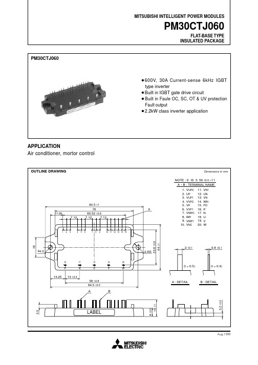
PM30CTJ060中文资料
PM30CTJ060PM30CTJ060FLAT-BASE TYPEINSULATED PACKAGEAPPLICATIONAir conditioner, mortor control ¡600V, 30A Current-sense 6kHz IGBT type inverter¡Built in IGBT gate drive circuit¡Built in Faule OC, SC, OT & UV protection Fault output¡2.2kW class inverter applicationA1.2.INSULATED PACKAGEV D = 15V, I CIN = 0mABase-plate Temperature detection, V D = 15V –20°C ≤ T j ≤ 125°C (only N side)V D = 15V, V FO = 15V TcINSULATED PACKAGEmA mA A A µs °C °C V V mA mA ms351055———120—12.5—0.0115—255334669101109012.012.5—101.8Min. V N1-V NC V XP1-V XPCApplied between : U P -V UPC , V P -V VPC , W P -V WPCU N · V N · W N -V NC–20°C ≤ T j ≤ 125°C, V D = 15V (only N side)–20°C ≤ T j ≤ 125°C, V D = 15V (only N side)V D = 15V V D = 15VCollector-emitter saturation voltage Collector-emitter cutoff currentTOTAL SYSTEMParameterSymbol Supply voltage protectedby OC & SCSupply voltageSupply voltage (surge)Module case operating temperature Storage temperature Isolation voltageConditionsV CC V CC(surge)T C T stg V iso Ratings V CC(PROT)400450500–20 ~ +100–40 ~ +1252500Unit V V °C °C V rmsV V D = 13.5 ~ 16.5V,Inverter part, T j = 125°C startApplied between : P-N, operating timeApplied between : P-N, surge and non-operating time (Note 1)60Hz, sinusoidal, AC · 1 minNote 1 : T C measuring point is as shown below.Min.Typ.Max.–I C = 30A, V D = 15V, I CIN = 0mA T j = 25°C T j = 125°CV mAUnit ParameterSymbol Test conditionsV CE(sat)I CESV EC t on t rr t c(on)t off t c(off)Limits V µs µs µs µs µs 2.63.03.52.0—0.94.02.0110———0.5——————1.82.02.51.00.10.33.01.0——I C = 30A, T j = 25°C I C = 30A, T j = 125°CFWDi forward voltageSwitching timeV D = 15V, I CIN = 0mA ↔10mA V CC = 300V, I C = 30A T j = 125°C(Per 1 arm) Inductive Load V CE = V CES , I CIN = 0mAELECTRICAL CHARACTERISTICS (Tj = 25°C, unless otherwise noted)INVERTER PARTV D = 15V, I CIN = 10mA Input on threshold current Input off threshold current Over current trip level Short circuit trip level Over current delay time Minimum fault output pulse width (Note 2)——1141——100—11.5———1.0Over temperature protection Supply circuit under voltage protectionFault output current (Note 2)Trip level Reset levelTrip levelReset level Note 2 :Fault output is given only when the internal OC, SC, OT & UV protection. (only N side)Fault output of OC, SC protection given pulse.Fault output of OT, UV protection given pulse while over level. (OT is only N side)Circuit currentParameterSymbol Test conditionsMax.Typ.Unit Limits CONTROL PARTI D mA I th(ON)I th(OFF)OC SC t off(OC)OT OT r UV UV r I FO(H)I FO(L)t FOINSULATED PACKAGEApplied between : P-NApplied between : V UP1-V UPC , V VP1-V VPCV WP1-V WPC , V N1-V NC (Note 3)Using application circuit Opto-coupler’s input signal Using application circuit Opto-coupler’s input signalApplied between : U P , V P , W P , U N , V N , W NV CC I CIN(ON)I CIN(OFF)f PWM t deadV mA mA kHz µsInput on current Input off currentPWM input frequencyArm shoot-through blocking timeV D Supply voltageV Note 3 : Permissible ripple value : dv/dt ≤ ±5V/µs, Vripple ≤ 2V P-PInverter IGBT part, per 1/6 module Inverter FWDi part, per 1/6 moduleCase to fin, thermal grease applied, per 1/6 moduleTHERMAL RESISTANCESSymbol ParameterTest conditionsUnit R th(j-c)Q R th(j-c)F R th(c-f)°C / W °C / W °C / WLimits Min.Tye.Max.——————1.54.50.4Junction to case thermal resistances Contact thermal resistance0.9810—MECHANICAL RATINGS AND CHARACTERISTICSSymbol ParameterTest conditionsLimits Unit N·m kg·cm g1.4715—1.181280Min.Tye.Max.—Mounting torque Mounting screw : M4—WeightRECOMMENDED CONDITIONS FOR USESymbol ParameterTest conditionsRatings Unit 15±1.5≤ 400≥ 5≤ 1≤ 8≥ 3.5INSULATED PACKAGE TNEINSULATED PACKAGE。
BSM30GP60中文资料

I C [A ]V CE [V]I C [A ]V CE [V]I C [A ]V GE [V]I F [A ]V F [V]300 V 33 OhmE [m W s ]I C [A]300 VE [m W s ]R G [Ω]Schaltverluste Wechselr. (typisch) E on = f (I C ), E off = f (I C ), E rec = f (I C ) V CC =Switching losses Inverter (typical) T j = 125°C, V GE = ±15 V, R Gon = R Goff =Z t h J C [K /W ]t [s]33 OhmI C [A ]V CE [V]I C [A ]V CE [V]I F [A ]V F [V]I F [A ]V F [V]R [Ω]T C [°C]Technische Information / Technical InformationIGBT-ModuleIGBT-Modules BSM30GP60Schaltplan/ Circuit diagramGehäuseabmessungen/ Package outlinesMit dieser technischen Information werden Halbleiterbauelemente spezifiziert, jedoch keine Eigenschaften zugesichert. Sie gilt in Verbindung mit den zugehörigen Technischen Erläuterungen.This technical information specifies semiconductor devices but promises no characteristics. It is valid in combination with the belonging technical notes.Terms & Conditions of UsageAttentionThe present product data is exclusively subscribed to technically experienced staff. This Data Sheet is describing the specification of the products for which a warranty is granted exclusively pursuant the terms and conditions of the supply agreement. There will be no guarantee of any kind for the product and its specifications. Changes to the Data Sheet are reserved.You and your technical departments will have to evaluate the suitability of the product for the intended application and the completeness of the product data with respect to such application. Should you require product information in excess of the data given in the Data Sheet, please contact your local Sales Office via “ / sales & contact”.WarningDue to technical requirements the products may contain dangerous substances. For information on the types in question please contact your local Sales Office via “ / sales & contact”.。
LA100-P_06中文资料
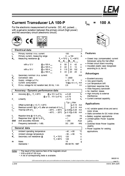
50
mA
1 : 2000
± 12 .. 15
V
10 (@ ±15 V) + IS mA
2.5
kV
Accuracy - Dynamic performance data
X
Accuracy @ IPN , TA = 25°C
@ ± 15 V (± 5 %) ± 0.45
%
@ ± 12 .. 15 V (± 5 %) ± 0.70
Frequency bandwidth (- 1 dB)
< 500 <1 > 200 DC .. 200
ns µs A/µ s kHz
General data
TA
ቤተ መጻሕፍቲ ባይዱ
Ambient operating temperature
T
Ambient storage temperature
S
R S Secondary coil resistance @
LEM
LEM reserves the right to carry out modifications on its transducers, in order to improve them, without previous notice.
060201/8
page 2/2
• Printed circuit board mounting • Insulated plastic case recognized
according to UL 94-V0.
Advantages
• Excellent accuracy • Very good linearity • Low temperature drift • Optimized response time • Wide frequency bandwidth • No insertion losses • High immunity to external
基于智能功率模块PM30RSF060的驱动和保护电路设计

基于智能功率模块PM30RSF060的驱动和保护电路设计第5卷第3期长沙航空职业技术学院学报Vo1.5No .32005年9⽉CHANGS HA AERONAUT C AL VOC ATI O NAL AND TECHN I C AL C OLLEGE JOURNALSep.2005基于智能功率模块P M30RSF060的驱动和保护电路设计陈军平1,杨国辉2,钟川桃2(11国防科技⼤学机电⼯程与⾃动化学院,湖南长沙 410073;21长沙航空职业技术学院,湖南长沙 410124)摘要:介绍智能功率模块P M30RSF060的原理与特性,在此基础上,提出⼀种基于P M30RSF060的驱动和保护电路设计⽅案。
实际应⽤表明,此⽅案作为基于直流⽆刷电机驱动的稳定控制平台的驱动单元,具有良好的控制效果。
关键词:I P M;驱动电路;保护电路;设计中图分类号:T N702 ⽂献标识码:A ⽂章编号:1671-9654(2005)03-035-04收稿⽇期:2005-05-18作者简介:陈军平(1975-),湖南涟源⼈,讲师,在读硕⼠研究⽣,研究⽅向:机电测控系统。
The D esi gn of D r i ve &Protecti on C i rcu it Ba sed on I P M P M 30RSF 060CHE N Jun -Ping 1,Y ANG Guo -Hui 2,Z HONG Chuan -Tao2(1.The College of E lectro m echanica l Eng ineering and A u to m ation,N ational U n iversity of D efense Tech 2nology,Changsha Hunan 410073;2.Changsha A eronautica l vocationd and Technical college,Chan 2gsha Hunan 410124)Abstract:The p rinci p le and characteristic of I ntelligent PowerModule (I P M )has been intr oduced firstly in this paper .Based on it,a designing sche me of drive &p r otecti on circuit has been p r oposed .A s a drive unit of stabilizati on contr ol flat driven by no -brush direct current electr omot or,the p ractical app licati on shows the designing sche me has better contr ol effect .Key words:I P M;drive circuit;p r otecti on circuit;design1 引⾔智能功率模块(I P M )是I ntelligent Power Mod 2ule 的缩写,是⼀种先进的功率开关器件,具有GTR (⼤功率晶体管)⾼电流密度、低饱和电压和耐⾼压的优点,以及MOSFET (场效应晶体管)⾼输⼊阻抗、⾼开关频率和低驱动功率的优点。
SPD30P06P中文资料
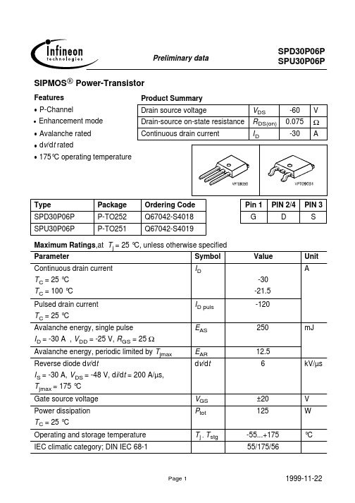
Symbol
Values
Unit
min. typ. max.
IS
-
-
-30 A
ISM
-
- -120
VSD
- -1.3 -1.7 V
trr
- 64.6 97 ns
Qrr
- 153 230 nC
Page 4
1999-11-22
元器件交易网
Ptot ID
Preliminary data
RDS(on) = f (ID)
parameter: VGS
SPD30P06P
0.26
W
c
0.22
d
e
f
g
h
i
0.20
0.18
0.16
0.14
0.12
0.10
j
0.08
k
0.06
0.04 0.02
VGS [V] =
c def -5.0 -5.5 -6.0 -6.5
ghi j k -7.0 -7.5 -8.0 -9.0 -10.0
0.00 0
-10 -20 -30 -40 A
-60
ID
Typ. transfer characteristics ID= f ( VGS )
³ VDS 2 x ID x RDS(on)max
parameter: tp = 80 µs
-60
Typ. forward transconductance gfs = f(ID); Tj=25°C parameter: gfs
ID
TC = 25 °C
TC = 100 °C
Pulsed drain current
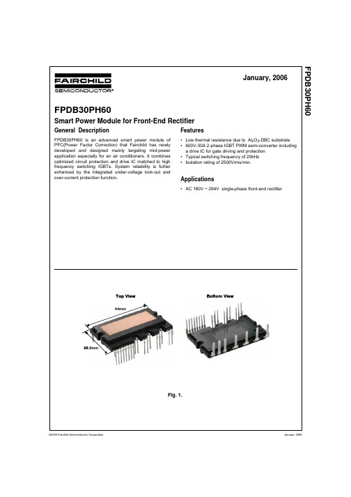
FPDB30PH60中文资料
©2005 Fairchild Semiconductor Corporation FPDB30PH60January, 200626.8mm44mmBottom View©2005 Fairchild Semiconductor Corporation FPDB30PH60January, 2006©2005 Fairchild Semiconductor Corporation FPDB30PH60January, 2006©2005 Fairchild Semiconductor Corporation FPDB30PH60January, 2006Absolute Maximum Ratings (T J = 25°C, Unless Otherwise Specified)Converter PartNote1.The maximum junction temperature rating of the power chips integrated within the SPM is 150 °C(@T C ≤ 100°C). However, to insure safe operation of the SPM,the average junction temperature should be limited to T J(ave) ≤ 125°C (@T C ≤ 100°C)Control PartTotal SystemThermal ResistanceNote :2. For the measurement point of case temperature(T C ), please refer to Fig. 2.ItemSymbol ConditionRating Unit Supply Voltage V i Applied between R-S 264V RMS Supply Voltage (Surge)V i(Surge)Applied between R-S 500V Output Voltage V PN Applied between P- N 450V Output Voltage (Surge)V PN(Surge)Applied between P- N500V Collector-emitter Voltage V CES 600V Input Current (100% Load)I i T C < 95°C, V i =220V, V PN = 390V, V PWM =20kHz20A Input Current (125% Load)I i(125%)T C < 95°C, V i =220V, V PN = 390V, V PWM =20kHz, 1min Non-repetitive 25A Collector DissipationP C T C = 25°C per One IGBT 83W Power Rating of Shunt Resistor P RSH T C < 125°C 2W Operating Junction TemperatureT J(Note 1)-20 ~ 125°CItemSymbol Condition RatingUnit Control Supply Voltage V CC Applied between V CC - COM 20V Input Signal Voltage V IN Applied between IN - COM -0.3~5.5V Fault Output Supply Voltage V FO Applied between V FO - COM -0.3~V CC +0.3V Fault Output CurrentI FO Sink Current at V FO Pin 5mA Current Sensing Input VoltageV SCApplied between C SC - COM-0.3~V CC +0.3VItemSymbol Condition RatingUnit Module Case Operation Temperature T C -20 ~ 100°C Storage Temperature T STG -40 ~ 125°C Isolation VoltageV ISO60Hz, Sinusoidal, AC 1 minute, Connection Pins to DBC2500V rmsItemSymbolCondition Min.Typ.Max.Unit Junction to Case Thermal Resistance(Referenced to PKG cen-ter)R θ(j-c)Q IGBT-- 1.2°C/W R θ(j-c)HD High-side diode -- 2.0°C/W R θ(j-c)LD Low-side diode-- 1.4°C/W©2005 Fairchild Semiconductor Corporation FPDB30PH60January, 2006Electrical Characteristics (T J = 25°C, Unless Otherwise Specified)Converter PartNote3.t ON and t OFF include the propagation delay time of the internal drive IC. t C(ON) and t C(OFF) are the switching time of IGBT itself under the given gate driving condition internally. For the detailed information, please see Fig. 4Control PartNote4.The fault-out pulse width t FOD depends on the capacitance value of C FOD according to the following approximate equation : C FOD = 18.3 x 10⁻⁶ x t FOD [F]ItemSymbol Condition Min.Typ.Max.Unit IGBT saturation voltage V CE(sat)V CC =15V, V IN = 5V; I C =30A - 2.4 3.1V High-side diode voltage V FH I F = 30A - 1.9 2.5V Low-side diode voltage V FL I F = 30A- 1.2 1.6V Switching Timest ON V PN = 400V, V CC = 15V, I C =30A V IN = 0V ↔ 5V, Inductive Load (Note 3)-550-ns t C(ON)-200-ns t OFF -430-ns t C(OFF)-180-ns t rr -60-ns I rr-6-A Current sensing resistor R SENSE 1.8 2.0 2.2m ΩCollector - emitter Leakage CurrentI CESV CE = V CES--250µAItem Symbol ConditionMin.Typ.Max.Unit Quiescent V CC Supply Cur-rentI QCCL V CC = 15V, IN = 0V V CC - COM --26mA Fault Output Voltage V FOH V SC = 0V, V FO Circuit: 4.7k Ω to 5V Pull-up 4.5--V V FOL V SC = 1V, V FO Circuit: 4.7k Ω to 5V Pull-up --0.8V Over Current Trip Level V SC(ref)V CC = 15V 0.450.50.55V Supply Circuit Under-Voltage Protection UV CCD Detection Level 10.711.913.0V UV CCR Reset Level11.212.413.2V Fault-out Pulse Width t FOD C FOD = 33nF (Note 4) 1.4 1.8 2.0ms ON Threshold Voltage V IN(ON)Applied between IN - COM3.0--V OFF Threshold Voltage V IN(OFF)--0.8V Resistance of ThermistorR TH@ T C = 25°C (Note Fig. 9)-50-k Ω@ T C = 80°C (Note Fig. 9)- 5.76-k Ω©2005 Fairchild Semiconductor Corporation FPDB30PH60January, 2006©2005 Fairchild Semiconductor Corporation FPDB30PH60January, 2006©2005 Fairchild Semiconductor Corporation FPDB30PH60January, 2006©2005 Fairchild Semiconductor Corporation FPDB30PH60January, 2006©2005 Fairchild Semiconductor Corporation FPDB30PH60January, 2006©2005 Fairchild Semiconductor Corporation FPDB30PH60January, 2006DISCLAIMERFAIRCHILD SEMICONDUCTOR RESERVES THE RIGHT TO MAKE CHANGES WITHOUT FURTHER NOTICE TO ANYPRODUCTS HEREIN TO IMPROVE RELIABILITY , FUNCTION OR DESIGN. FAIRCHILD DOES NOT ASSUME ANY LIABILITY ARISING OUT OF THE APPLICATION OR USE OF ANY PRODUCT OR CIRCUIT DESCRIBED HEREIN; NEITHER DOES IT CONVEY ANY LICENSE UNDER ITS PATENT RIGHTS, NOR THE RIGHTS OF OTHERS.TRADEMARKSThe following are registered and unregistered trademarks Fairchild Semiconductor owns or is authorized to use and is not intended to be an exhaustive list of all such trademarks.LIFE SUPPORT POLICYFAIRCHILD’S PRODUCTS ARE NOT AUTHORIZED FOR USE AS CRITICAL COMPONENTS IN LIFE SUPPORTDEVICES OR SYSTEMS WITHOUT THE EXPRESS WRITTEN APPROVAL OF FAIRCHILD SEMICONDUCTOR CORPORATION.As used herein:1. Life support devices or systems are devices orsystems which, (a) are intended for surgical implant intothe body, or (b) support or sustain life, or (c) whosefailure to perform when properly used in accordancewith instructions for use provided in the labeling, can be reasonably expected to result in significant injury to the user.2. A critical component is any component of a life support device or system whose failure to perform can be reasonably expected to cause the failure of the life support device or system, or to affect its safety or effectiveness.PRODUCT STATUS DEFINITIONS Definition of Terms Datasheet Identification Product Status DefinitionAdvance InformationPreliminary No Identification Needed Obsolete This datasheet contains the design specifications for product development. Specifications may change in any manner without notice.This datasheet contains preliminary data, andsupplementary data will be published at a later date.Fairchild Semiconductor reserves the right to make changes at any time without notice in order to improve design.This datasheet contains final specifications. Fairchild Semiconductor reserves the right to make changes at any time without notice in order to improve design.This datasheet contains specifications on a product that has been discontinued by Fairchild semiconductor.The datasheet is printed for reference information only.Formative or In DesignFirst ProductionFull ProductionNot In ProductionISOPLANAR™ LittleFET™MICROCOUPLER™MicroFET™MicroPak™MICROWIRE™MSX™MSXPro™OCX™OCXPro™OPTOLOGIC ®OPTOPLANAR™PACMAN™POP™Power247™PowerEdge™FAST ®FASTr™ FPS™FRFET™GlobalOptoisolator™GTO™HiSeC™I 2C™i-Lo ™ImpliedDisconnect™IntelliMAX™Rev. I18ACEx™ActiveArray™Bottomless™Build it Now™CoolFET™CROSSVOLT ™DOME™EcoSPARK™E 2CMOS™EnSigna™FACT™FACT Quiet Series™PowerSaver™PowerTrench ®QFET ®QS™QT Optoelectronics™Quiet Series™RapidConfigure™RapidConnect™μSerDes™ScalarPump™SILENT SWITCHER®SMART START™SPM™Stealth™SuperFET™SuperSOT™-3SuperSOT™-6SuperSOT™-8SyncFET™ TCM™ TinyLogic ®TINYOPTO™TruTranslation™UHC™UltraFET ®UniFET™VCX™Wire™Across the board. Around the world.™The Power Franchise ®Programmable Active Droop™。
330R100M063JS8中文资料(List Unclassifed)中文数据手册「EasyDatasheet - 矽搜」

(PBB)和多溴 二苯醚(PBDE).
50V 63 & 75 V 100至 250伏 1.02"直 径 6.3 & 7.5 V 10至 40 V 50V
0.75 0.80 1.00 1.27 1.42 1.50
1.52
0.75 0.80 1.00 1.26 1.40 1.48
1.50
0.76 0.81 1.00 1.25 1.38 1.46
1.25
0.78 0.83 1.00 1.20 1.30 1.35
1.36
50V
0.76 0.81 1.00 1.25 1.38 1.45
1.47
63 & 75 V
0.74 0.80 1.00 1.28 1.43 1.52
1.54
100至 250伏
0.76 0.81 1.00 1.24 1.37 1.44
工作温度: 额定电压: 电容:
容量偏差: 泄漏电流: 冷阻抗:
纹波电流乘法器:
-55°C至+105° C 6.3至250 VDC 270μF至33000μF6 .3至100伏; -10 + 75%,160至250 VDC; 10 + 50%≤0.5√CVμA,最大4毫安,5分钟. -55°C25°CZ≤4倍数为6.3和7.5 V,3为10〜50 V,
15000 330153U010HS2
23.7 13.7 7.66 9.49
15000 330R153U010HS2
17.0 9.3 9.05 11.50
18000 330183U010HT2
20.5 11.9 8.81 10.90
18000 330R183U010HT2
FAIRCHILD FQPF30N06L 数据手册
现货库存、技术资料、百科信息、热点资讯,精彩尽在鼎好!FQPF30N06LTO-220FG SDNotes:1. Repetitive Rating : Pulse width limited by maximum junction temperature2. L = 810µH, I AS = 22.5A, V DD = 25V, R G = 25 Ω, Starting T J = 25°C3. I SD ≤ 32A, di/dt ≤ 300A/us, V DD ≤ BV DSS, Starting T J = 25°C4. Pulse Test : Pulse width ≤300us, Duty cycle ≤2%5. Essentially independent of operating temperature/ ∆T J CoefficientD I DSS Zero Gate Voltage Drain Current V DS = 60 V, V GS = 0 V ----1µA V DS = 48 V, T C = 150°C ----10µA I GSSF Gate-Body Leakage Current, Forward V GS = 20 V, V DS = 0 V ----100nA I GSSRGate-Body Leakage Current, ReverseV GS = -20 V, V DS = 0 V-----100nAOn CharacteristicsV GS(th)Gate Threshold Voltage V DS = V GS , I D = 250 µA1.0--2.5V R DS(on)Static Drain-Source On-ResistanceV GS = 10 V, I D = 11.3 AV GS = 5 V, I D =11.3 A ----0.0270.0350.0350.045Ωg FSForward TransconductanceV DS = 25 V, I D = 11.3 A --22--SDynamic CharacteristicsC iss Input Capacitance V DS = 25 V, V GS = 0 V, f = 1.0 MHz--8001040pF C oss Output Capacitance--270350pF C rssReverse Transfer Capacitance--5065pFSwitching Characteristicst d(on)Turn-On Delay Time V DD = 30 V, I D = 16 A,R G = 25 Ω--1540ns t r Turn-On Rise Time --210430ns t d(off)Turn-Off Delay Time --60130ns t f Turn-Off Fall Time --110230ns Q g Total Gate Charge V DS = 48 V, I D = 32 A,V GS = 5 V--1520nC Q gs Gate-Source Charge -- 3.5--nC Q gdGate-Drain Charge--8.5--nCDrain-Source Diode Characteristics and Maximum RatingsI S Maximum Continuous Drain-Source Diode Forward Current ----22.5A I SM Maximum Pulsed Drain-Source Diode Forward Current----90A V SD Drain-Source Diode Forward Voltage V GS = 0 V, I S = 22.5 A ---- 1.5V t rr Reverse Recovery Time V GS = 0 V, I S = 32 A,dI F / dt = 100 A/µs --60--ns Q rrReverse Recovery Charge--90--nC(Note 4)(Note 4, 5)(Note 4, 5)(Note 4)TRADEMARKSThe following are registered and unregistered trademarks Fairchild Semiconductor owns or is authorized to use and is not intended to be an exhaustive list of all such trademarks.DISCLAIMERFAIRCHILD SEMICONDUCTOR RESERVES THE RIGHT TO MAKE CHANGES WITHOUT FURTHER NOTICE TO ANY PRODUCTS HEREIN TO IMPROVE RELIABILITY, FUNCTION OR DESIGN. FAIRCHILD DOES NOT ASSUME ANY LIABILITY ARISING OUT OF THE APPLICATION OR USE OF ANY PRODUCT OR CIRCUIT DESCRIBED HEREIN;NEITHER DOES IT CONVEY ANY LICENSE UNDER ITS PATENT RIGHTS, NOR THE RIGHTS OF OTHERS.LIFE SUPPORT POLICYFAIRCHILD’S PRODUCTS ARE NOT AUTHORIZED FOR USE AS CRITICAL COMPONENTS IN LIFE SUPPORT DEVICES OR SYSTEMS WITHOUT THE EXPRESS WRITTEN APPROVAL OF FAIRCHILD SEMICONDUCTOR CORPORATION.As used herein:1. Life support devices or systems are devices or systems which, (a) are intended for surgical implant into the body,or (b) support or sustain life, or (c) whose failure to perform when properly used in accordance with instructions for use provided in the labeling, can be reasonably expected to result in significant injury to the user.2. A critical component is any component of a life support device or system whose failure to perform can be reasonably expected to cause the failure of the life support device or system, or to affect its safety or effectiveness.PRODUCT STATUS DEFINITIONS Definition of TermsDatasheet Identification Product Status DefinitionAdvance InformationFormative or In Design This datasheet contains the design specifications for product development. Specifications may change in any manner without notice.PreliminaryFirst ProductionThis datasheet contains preliminary data, andsupplementary data will be published at a later date.Fairchild Semiconductor reserves the right to make changes at any time without notice in order to improve design.No Identification Needed Full ProductionThis datasheet contains final specifications. Fairchild Semiconductor reserves the right to make changes at any time without notice in order to improve design.Obsolete Not In ProductionThis datasheet contains specifications on a product that has been discontinued by Fairchild semiconductor.The datasheet is printed for reference information only.ACEx™Bottomless™CoolFET™CROSSVOLT™DenseTrench™DOME™EcoSPARK™E 2CMOS™EnSigna™FACT™FACT Quiet Series™FAST ®FASTr™FRFET™GlobalOptoisolator™GTO™HiSeC™ISOPLANAR™LittleFET™MicroFET™MICROWIRE™OPTOLOGIC™OPTOPLANAR™PACMAN ™POP™PowerTrench ®QFET™QS™QT Optoelectronics™Quiet Series™SLIENT SWITCHER ®SMART START™Stealth™SuperSOT™-3SuperSOT™-6SuperSOT™-8SyncFET™TinyLogic™UHC™UltraFET ®VCX™。
30N06中文资料
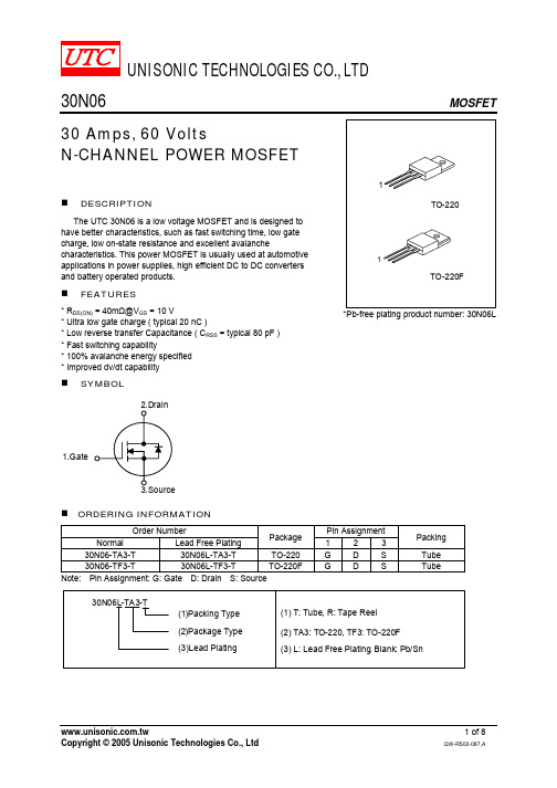
UNISONIC TECHNOLOGIES CO., LTD30N06MOSFET30 Amps, 60 VoltsN-CHANNEL POWER MOSFETDESCRIPTIONThe UTC 30N06 is a low voltage MOSFET and is designed to have better characteristics, such as fast switching time, low gate charge, low on-state resistance and excellent avalanchecharacteristics. This power MOSFET is usually used at automotive applications in power supplies, high efficient DC to DC converters and battery operated products.FEATURES* R DS(ON) = 40m Ω@V GS = 10 V* Ultra low gate charge ( typical 20 nC )* Low reverse transfer Capacitance ( C RSS = typical 80 pF ) * Fast switching capability* 100% avalanche energy specified * Improved dv/dt capabilitySYMBOL1.GateTO-22011TO-220F*Pb-free plating product number: 30N06LORDERING INFORMATIONOrder Number Pin AssignmentNormal Lead Free Plating Package 1 2 3Packing30N06-TA3-T 30N06L-TA3-T TO-220 G D S Tube 30N06-TF3-T 30N06L-TF3-T TO-220F G D S Tube Note: Pin Assignment: G: Gate D: Drain S: SourceABSOLUTE MAXIMUM RATINGSPARAMETER SYMBOL RATINGS UNITDrain-Source Voltage V DSS 60 V Gate to Source Voltage V GSS ±20 VT C = 25 30 AContinuous Drain Current T C = 100 I D21.3 APulsed Drain Current (Note 1) I DM 120 A Avalanche Energy, Single Pulsed (Note 2) E AS 300 mJ Repetitive Avalanche Energy (Note 1) E AR 8 mJ Peak Diode Recovery dv/dt (Note 3) dv/dt 7.5 V/nsTotal Power Dissipation (T C = 25 ) 80 WDerating Factor Above 25P D0.53 W/ Operation Junction Temperature T J -55 ~ +150 Storage Temperature T STG -55 ~ +150Note: Absolute maximum ratings are those values beyond which the device could be permanently damaged.Absolute maximum ratings are stress ratings only and functional device operation is not implied.THERMAL DATAPARAMETER SYMBOL MIN TYP MAX UNITThermal Resistance, Junction-to-Case θJC 1.8 °C/W Thermal Resistance, Case-to-Sink θCS 0.5 °C/W Thermal Resistance, Junction-to-Ambient θJA 62.5 °C/WELECTRICAL CHARACTERISTICS (T C = 25 , unless otherwise specified)PARAMETER SYMBOL TEST CONDITIONS MIN TYP MAX UNIT Off CharacteristicsDrain-Source Breakdown Voltage BV DSS V GS = 0 V, I D = 250 µA 60 VV DS = 60 V, V GS = 0 V 1 µADrain-Source Leakage Current I DSSV DS = 48 V, V GS = 0 V, T J = 150 10µA Forward V GS = 20V, V DS = 0 V 100nAGate-Source Leakage Current Reverse I GSSV GS = -20V, V DS = 0 V -100nA Breakdown Voltage TemperatureCoefficientBV DSS /△T J I D = 250 µA, Referenced to 25 0.06 V/On Characteristics Gate Threshold Voltage V GS(TH) V DS = V GS , I D = 250 µA 2.0 4.0V Static Drain-Source On-StateResistanceR DS(ON) V GS = 10 V, I D = 15 A 32 40m ΩDynamic Characteristics Input Capacitance C ISS 800 pFOutput Capacitance C OSS 300 pFReverse Transfer Capacitance C RSSV GS = 0 V, V DS = 25 V f = 1MHz 80 pF Switching Characteristics Turn-On Delay Time t D(ON) 12 nsTurn-On Rise Time t R 79 ns Turn-Off Delay Time t D(OFF) 50 nsTurn-Off Fall Time t F V DD = 30V, I D =15 A, V GS =10V (Note 4, 5) 52 ns Total Gate Charge Q G 20 30nCGate-Source Charge Q GS 6 nCGate-Drain Charge (Miller Charge) Q GD V DS = 60V, V GS = 10 V, I D = 24A(Note 4, 5)9 nCELECTRICAL CHARACTERISTICS (Cont.)Note 1. Repeativity rating: pulse width limited by junction temperature2. L=19.5mH, I AS=30A, R G=20Ω, Starting T J=253. I SD≤50A, di/dt≤300A/µs, V DD≤BV DSS, Starting T J=254. Pulse Test: Pulse Width≤300µs,Duty Cycle≤2%5. Essentially independent of operating temperature.TEST CIRCUITS AND WAVEFORMSV DDV GS (Driver)I SD (D.U.T.)Body DiodeForward Voltage DropV DS(D.U.T.)Fig. 1A Peak Diode Recovery dv/dt Test CircuitFig. 1B Peak Diode Recovery dv/dt WaveformsTEST CIRCUITS AND WAVEFORMS (Cont.)R LDDV DS90%10%V GStFig. 2A Switching Test Circuit Fig. 2B Switching WaveformsFig. 3A Gate Charge Test CircuitFig. 3B Gate Charge Waveform10VLV DDI ASFig. 4A Unclamped Inductive Switching Test Circuit Fig. 4B Unclamped Inductive Switching WaveformsTYPICAL CHARACTERISTICS101010101010Drain -Source Voltage , V DS (V)D r a i n C u r r e n t , I D (A )On-State CharacteristicsGate-Source Voltage , V GS (V)Transfer CharacteristicsD r a i n -S o u r c e O n -R e s i s t a n c e , R D S (O N ) (m Ω)Drain Current , I D (A)408010020406080On-Resistance Variation vs . Drain Current and102101000.2Source-Drain Voltage , V SD (V)R e v e r s e D r a i n C u r r e n t , I S D (A )Reverse Drain Current vs . Allowable CaseTemperature 1.60.40.60.8 1.0 1.2 1.420601200.1Drain -Source Voltage, V DC (V)C a p a c i t a n c e (p F )Capacitance Characteristics1Total Gate Charge , Q G (nC)Gate Charge Characteristics10TYPICAL CHARACTERISTICS(Cont.)-100D r a i n -S o u r c e B r e a k d ow n V o l t a g e , B V D S S (N o r m a l i z e d )Junction Temperature , T J (℃)-5050200100150Breakdown Voltage Variation vs . JunctionD r a i n -S o u r c e On -R e s i s t a n c e , R D S (O N ), (N o r m a l i z e d )-5050100150On-Resistance Variation vs . 01.0Junction Temperature , T J (℃)0.1Drain -Source Voltage, V DS (V)D r a i n C u r r e n t , I D ,(A )Maximum Safe Operating1100Case Temperature, T C (℃)Maximum Drain Current vs . Case Temperature 101001000Square Wave Pulse Duration , t 1 (sec)T h e r m a l R e s p o n s e , Z θJ C (t )11E-50.10.110Transient Thermal Response Curve1E-41E-30.01。
FPDB30PH60中文资料
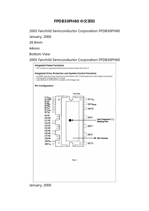
FPDB30PH60中文资料2005 Fairchild Semiconductor Corporation FPDB30PH60 January, 200626.8mm44mmBottom View2005 Fairchild Semiconductor Corporation FPDB30PH60January, 20062005 Fairchild Semiconductor Corporation FPDB30PH60January, 20062005 Fairchild Semiconductor Corporation FPDB30PH60 January, 2006Absolute Maximum Ratings (T J = 25°C, Unless Otherwise Specified)Converter PartNote1.The maximum junction temperature rating of the power chips integrated within the SPM is 150 °C(@T C ≤ 100°C). However, to insure safe operation of the SPM,the average junction temperature should be limited to T J(ave) ≤ 125°C (@T C ≤ 100°C)Control PartTotal SystemThermal ResistanceNote :2. For the measurement point of case temperature(T C ), please refer to Fig. 2.ItemSymbol ConditionRating Unit Supply Voltage V i Applied between R-S 264V RMS Supply Voltage (Surge)V i(Surge)Applied between R-S 500V Output Voltage V PN Applied between P- N 450V Output Voltage (Surge)V PN(Surge)Applied between P- N500V Collector-emitter Voltage V CES 600V Input Current (100% Load)I i T C < 95°C, V i =220V, V PN = 390V, V PWM =20kHz20A Input Current (125% Load)I i(125%)T C < 95°C, V i =220V, V PN = 390V, V PWM =20kHz, 1min Non-repetitive 25A Collector DissipationP C T C = 25°C per One IGBT 83W Power Rating of Shunt Resistor P RSH T C < 125°C 2W Operating Junction Temperature T J(Note 1)-20 ~ 125°CItemSymbol Condition RatingUnit Control Supply Voltage V CC Applied between V CC - COM 20V Input Signal Voltage V IN Applied between IN - COM -0.3~5.5V Fault Output Supply Voltage V FO Applied between V FO - COM -0.3~V CC +0.3V Fault Output CurrentI FO Sink Current at V FO Pin 5mA Current Sensing Input VoltageV SCApplied between C SC - COM-0.3~V CC +0.3VItemSymbol Condition RatingUnit Module Case Operation Temperature T C -20 ~ 100°C Storage Temperature T STG -40 ~ 125°C Isolation Voltage V ISO60Hz, Sinusoidal, AC 1 minute, Connection Pins to DBC2500V rmsItemSymbolCondition Min.Typ.Max.Unit Junction to Case Thermal Resistance(Referenced to PKG cen-ter)R θ(j-c)Q IGBT-- 1.2°C/W R θ(j-c)HD High-side diode -- 2.0°C/W R θ(j-c)LD Low-side diode-- 1.4°C/W2005 Fairchild Semiconductor Corporation FPDB30PH60January, 2006Electrical Characteristics (T J = 25°C, Unless Otherwise Specified)Converter PartNote3.t ON and t OFF include the propagation delay time of the internal drive IC. t C(ON) and t C(OFF) are the switching time of IGBT itself under the given gate driving condition internally. For the detailed information, please see Fig. 4Control PartNote4.The fault-out pulse width t FOD depends on the capacitance value of C FOD according to the following approximate equation : C FOD = 18.3 x 10⁻⁶ x t FOD [F] ItemSymbol Condition Min.Typ.Max.Unit IGBT saturation voltage V CE(sat)V CC =15V, V IN = 5V; I C =30A - 2.4 3.1V High-side diode voltage V FH I F = 30A - 1.9 2.5V Low-side diode voltage V FL I F = 30A - 1.2 1.6V Switching Timest ON V PN = 400V, V CC = 15V, I C =30A V IN = 0V ? 5V, Inductive Load (Note 3)-550-ns t C(ON)-200-ns t OFF -430-ns t C(OFF)-180-ns t rr -60-ns I rr-6-A Current sensing resistor R SENSE 1.8 2.0 2.2m ?Collector- emitter Leakage CurrentI CESV CE = V CES--250μAItem Symbol ConditionMin.Typ.Max.Unit Quiescent V CC Supply Cur-rentI QCCL V CC = 15V, IN = 0V V CC - COM --26mA Fault Output Voltage V FOH V SC = 0V, V FO Circuit: 4.7k ? to 5V Pull-up 4.5--V V FOL V SC = 1V, V FO Circuit: 4.7k ? to 5V Pull-up --0.8V Over Current Trip Level V SC(ref)V CC = 15V 0.450.50.55V Supply Circuit Under-Voltage Protection UV CCD Detection Level10.711.913.0V UV CCR Reset Level11.212.413.2V Fault-out Pulse Width t FOD C FOD = 33nF (Note 4) 1.4 1.8 2.0ms ON Threshold Voltage V IN(ON)Applied between IN - COM3.0--V OFF Threshold Voltage V IN(OFF)--0.8V Resistance of ThermistorR TH@ T C = 25°C (Note Fig. 9)-50-k ?@ T C = 80°C (Note Fig. 9) - 5.76-k ?2005 Fairchild Semiconductor Corporation FPDB30PH60January, 20062005 Fairchild Semiconductor Corporation FPDB30PH60January, 20062005 Fairchild Semiconductor Corporation FPDB30PH60January, 20062005 Fairchild Semiconductor Corporation FPDB30PH60January, 20062005 Fairchild Semiconductor Corporation FPDB30PH60January, 20062005 Fairchild Semiconductor Corporation FPDB30PH60January, 2006DISCLAIMERFAIRCHILD SEMICONDUCTOR RESERVES THE RIGHT TO MAKE CHANGES WITHOUT FURTHER NOTICE TO ANYPRODUCTS HEREIN TO IMPROVE RELIABILITY , FUNCTION OR DESIGN. FAIRCHILD DOES NOT ASSUME ANY LIABILITY ARISING OUT OF THE APPLICATION OR USE OF ANY PRODUCT OR CIRCUIT DESCRIBED HEREIN; NEITHER DOES IT CONVEY ANY LICENSE UNDER ITS PATENT RIGHTS, NOR THE RIGHTS OF OTHERS.TRADEMARKSThe following are registered and unregistered trademarks Fairchild Semiconductor owns or is authorized to use and is not intended to be an exhaustive list of all such trademarks.LIFE SUPPORT POLICYFAIRCHILD’S PRODUCTS ARE NOT AUTHORIZED FOR USE AS CRITICAL COMPONENTS IN LIFE SUPPORTDEVICES OR SYSTEMS WITHOUT THE EXPRESS WRITTEN APPROVAL OF FAIRCHILD SEMICONDUCTOR CORPORATION.As used herein:1. Life support devices or systems are devices orsystems which, (a) are intended for surgical implant intothe body, or (b) support or sustain life, or (c) whosefailure to perform when properly used in accordancewith instructions for use provided in the labeling, can be reasonably expected to result in significant injury to the user.2. A critical component is any component of a life support device or system whose failure to perform can be reasonably expected to cause the failure of the life support device or system, or to affect its safety or effectiveness.PRODUCT STATUS DEFINITIONS Definition of Terms Datasheet Identification Product Status DefinitionAdvance InformationPreliminary No Identification Needed Obsolete This datasheet contains the design specifications for productdevelopment. Specifications may change in any manner without notice.This datasheet contains preliminary data, andsupplementary data will be published at a later date.Fairchild Semiconductor reserves the right to make changes at any time without notice in order to improve design.This datasheet contains final specifications. Fairchild Semiconductor reserves the right to make changes at any time without notice in order to improve design.This datasheet contains specifications on a product that has been discontinued by Fairchild semiconductor.The datasheet is printed for reference information only.Formative or In DesignFirst ProductionFull ProductionNot In ProductionISOPLANAR?LittleFET?MICROCOUPLER?MicroFET?MicroPak?MICROWIRE?MS X?MSXPro?OCX?OCXPro?OPTOLOGIC ?OPTOPLANAR?PACMAN?POP?Power247?PowerEdge?FAST ?FASTr? FPS?FRFET?GlobalOptoisolator?GTO?HiSeC?I 2C?i-Lo ?ImpliedDisconnect?IntelliMAX?Rev. I18ACEx?ActiveArray?Bottomless?Build it Now?CoolFET?CROSSVOLT ?DOME?EcoSPARK?E 2CMOS?EnSigna?FACT?FACT Quiet Series?PowerSaver?PowerTrench ?QFET ?QS?QT Optoelectronics?Quiet Series?RapidConfigure?RapidConnect?μSerDes?ScalarPump?SILEN T SWITCHERSMART START?SPM?Stealth?SuperFET?SuperSOT?-3SuperSOT?-6SuperSOT?-8SyncFET? TCM? TinyLogic ?TINYOPTO?TruTranslation?UHC?UltraFET ?UniFET?VCX?Wire?Across the board. Around the world.?The Power Franchise ?Programmable Active Droop?。
RF1S30N06LESM资料
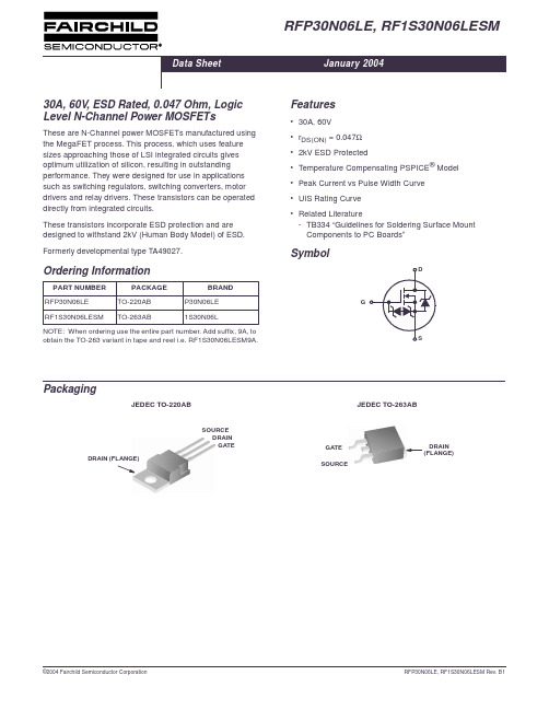
NOTE: 1. TJ = 25oC to 150oC.
Electrical Specifications
PARAMETER
TC = 25oC, Unless Otherwise Specified SYMBOL BVDSS VGS(TH) IDSS TEST CONDITIONS ID = 250µA, V GS = 0V, Figure 11 VGS = VDS, ID = 250µA, Figure 10 VDS = Rated BVDSS , VGS = 0 VDS = 0.8 x Rated B VDSS, VGS = 0, TC = 150oC MIN 60 1 VGS = 0V to 10V VGS = 0V to 5V VGS = 0V to 1V VDS = 25V, VGS = 0V, f = 1MHz Figure 12 VDD = 48V, ID = 30A, RL = 1.6Ω Figures 18, 19 TYP 11 88 30 40 51 28 1.8 1350 290 85 MAX 2 25 250 ±10 0.047 140 100 62 34 2.6 1.55 80 UNITS V V µA µA µA Ω ns ns ns ns ns ns nC nC nC pF pF pF
Drain to Source Voltage (Note 1) . . . . . . . . . . . . . . . . . . . . . . . . . . . . . . . . . . . . . VDSS Drain to Gate Voltage (R GS = 20kΩ) (Note 1) . . . . . . . . . . . . . . . . . . . . . . . . . . VDGR Gate to Source Voltage . . . . . . . . . . . . . . . . . . . . . . . . . . . . . . . . . . . . . . . . . . . . . VGS Continuous Drain Current . . . . . . . . . . . . . . . . . . . . . . . . . . . . . . . . . . . . . . . . . . . . .ID Pulsed Drain Current (Note 3) . . . . . . . . . . . . . . . . . . . . . . . . . . . . . . . . . . . . . . IDM Pulsed Avalanche Rating . . . . . . . . . . . . . . . . . . . . . . . . . . . . . . . . . . . . . . . . . . . . EAS Power Dissipation . . . . . . . . . . . . . . . . . . . . . . . . . . . . . . . . . . . . . . . . . . . . . . . . . . PD Derate Above 25oC . . . . . . . . . . . . . . . . . . . . . . . . . . . . . . . . . . . . . . . . . . . . . . . . . Electrostatic Discharge Rating, MIL-STD-883, Category B(2). . . . . . . . . . . . . . . .ESD Operating and Storage Temperature . . . . . . . . . . . . . . . . . . . . . . . . . . . . . . . TJ, TSTG Maximum Temperature for Soldering Leads at 0.063in (1.6mm) from Case for 10s. . . . . . . . . . . . . . . . . . . . . . . . . . . . TL Package Body for 10s, See Techbrief 334. . . . . . . . . . . . . . . . . . . . . . . . . . . . Tpkg
MBRP30060CT资料

Max 45 60 300 150 300 2500 2.0
Unit Volts
Amps Amps Amps Amps °C °C V/µs
*55 to +175 *55 to +150
10000 0.45
THERMAL CHARACTERISTICS PER LEG
Thermal Resistance, Junction to Case RθJC °C/W
©RectifierInc. 1996 Data Motorola, Device
1
元器件交易网 MBRP30045CT MBRP30060CT
PACKAGE DIMENSIONS
–A– R G –B–
W 0.25 (0.010) N
M
T A
M
B
M
NOTES: 1. DIMENSIONING AND TOLERANCING PER ANSI Y14.5M, 1982. 2. CONTROLLING DIMENSION: INCH. 3. TERMINAL PENETRATION: 5.97 (0.235) MAXIMUM. INCHES MIN MAX 3.450 3.635 0.700 0.810 0.615 0.640 0.120 0.130 0.435 0.445 1.370 1.380 0.007 0.030 1/4–20UNC–2B 0.270 0.285 31.50 BSC 0.600 0.630 0.330 0.375 0.170 0.190 MILLIMETERS MIN MAX 87.63 92.33 17.78 20.57 15.53 16.26 3.05 3.30 11.05 11.30 34.80 35.05 0.18 0.76 1/4–20UNC–2B 6.86 7.32 80.01 BSC 15.24 16.00 8.39 9.52 4.32 4.82
- 1、下载文档前请自行甄别文档内容的完整性,平台不提供额外的编辑、内容补充、找答案等附加服务。
- 2、"仅部分预览"的文档,不可在线预览部分如存在完整性等问题,可反馈申请退款(可完整预览的文档不适用该条件!)。
- 3、如文档侵犯您的权益,请联系客服反馈,我们会尽快为您处理(人工客服工作时间:9:00-18:30)。
Ordering Information
PART NUMBER RFG30P06 RFP30P06 RF1S30P06SM PACKAGE TO-247 TO-220AB TO-263AB BRAND RFG30P06 RFP3F1S30P06
S
NOTE: When ordering, use the entire part number. Add the suffix 9A to obtain the TO-263AB variant in tape and reel, i.e. RF1S30P06SM9A.
4-134
元器件交易网
Features
• 30A, 60V • rDS(ON) = 0.065Ω • Temperature Compensating PSPICE® Model • Peak Current vs Pulse Width Curve • UIS Rating Curve • 175oC Operating Temperature • Related Literature - TB334 “Guidelines for Soldering Surface Mount Components to PC Boards”
元器件交易网
RFG30P06, RFP30P06, RF1S30P06SM
Absolute Maximum Ratings
TC = 25oC, Unless Otherwise Specified RFG30P06, RFP30P06 RF1S30P06SM -60 -60 ±20 30 Refer to Peak Current Curve Refer to UIS Curve 135 0.9 -55 to 175 300 260 UNITS V V V A
Drain to Source Voltage (Note 1) . . . . . . . . . . . . . . . . . . . . . . . . . . . . . . . . . . . . . . .VDSS Drain to Gate Voltage (RGS = 20kΩ) (Note 1) . . . . . . . . . . . . . . . . . . . . . . . . . . . . VDGR Gate to Source Voltage . . . . . . . . . . . . . . . . . . . . . . . . . . . . . . . . . . . . . . . . . . . . . . .VGS Continuous Drain Current . . . . . . . . . . . . . . . . . . . . . . . . . . . . . . . . . . . . . . . . . . . . . . ID Pulsed Drain Current (Note 3) (Figure 5) . . . . . . . . . . . . . . . . . . . . . . . . . . . . . . . . IDM Single Pulse Avalanche Rating (Figure 6) . . . . . . . . . . . . . . . . . . . . . . . . . . . . . . . . . EAS Power Dissipation . . . . . . . . . . . . . . . . . . . . . . . . . . . . . . . . . . . . . . . . . . . . . . . . . . . . PD Linear Deratlng Factor . . . . . . . . . . . . . . . . . . . . . . . . . . . . . . . . . . . . . . . . . . . . . . . . . Operating and Storage Temperature . . . . . . . . . . . . . . . . . . . . . . . . . . . . . . . . . TJ, TSTG Maximum Temperature for Soldering Leads at 0.063in (1.6mm) from Case for 10s. . . . . . . . . . . . . . . . . . . . . . . . . . . . . . TL Package Body for 10s, See Techbrief 334 . . . . . . . . . . . . . . . . . . . . . . . . . . . . . . Tpkg
oC/W oC/W oC/W
Drain to Source Breakdown Voltage Gate Threshold Voltage Zero Gate Voltage Drain Current
Gate to Source Leakage Current Drain to Source On Resistance (Note 2) Turn-On Time Turn-On Delay Time Rise Time Turn-Off Delay Time Fall Time Turn-Off Time Total Gate Charge Gate Charge at -10V Threshold Gate Charge Input Capacitance Output Capacitance Reverse Transfer Capacitance Thermal Resistance, Junction to Case Thermal Resistance, Junction to Ambient
W W/oC oC
oC oC
CAUTION: Stresses above those listed in “Absolute Maximum Ratings” may cause permanent damage to the device. This is a stress only rating and operation of the device at these or any other conditions above those indicated in the operational sections of this specification is not implied.
NOTE: 1. TJ = 25oC to 150oC.
Electrical Specifications
PARAMETER
TC = 25oC, Unless Otherwise Specified SYMBOL BVDSS VGS(TH) IDSS IGSS rDS(ON) t(ON) td(ON) tr td(OFF) tf t(OFF) Qg(TOT) Qg(-10) Qg(TH) CISS COSS CRSS RθJC RθJA TO-220, TO-263 TO-247 VGS = 0 to -20V VGS = 0 to -10V VGS = 0 to -2V VDD = -48V, ID = 30A, RL = 1.6Ω, IG(REF) = 1.6mA TEST CONDITIONS ID = 250µA, VGS = 0V VGS = VDS, ID = 250µA VDS = -60V, VGS = 0V VDS = 0.8 x Rated BVDSS, TC = 150oC VGS = ±20V ID = -30A, VGS = -10V (Figure 9) VDD = -30V, ID = 15A, RL = 2.00Ω, VGS = -10V RG = 6.25Ω (Figure 13) MIN -60 -2 TYP 15 23 28 18 140 70 5.5 3200 800 175 MAX -4 -1 -25 ±100 0.065 80 100 170 85 6.6 1.11 62 30 UNITS V V µA µA nA Ω ns ns ns ns ns ns nC nC nC pF pF pF
元器件交易网
RFG30P06, RFP30P06, RF1S30P06SM
Data Sheet July 1999 File Number
2437.3
30A, 60V, 0.065 Ohm, P-Channel Power MOSFETs
These are P-Channel power MOSFETs manufactured using the MegaFET process. This process, which uses feature sizes approaching those of LSI circuits, gives optimum utilization of silicon, resulting in outstanding performance. They are designed for use in applications such as switching regulators, switching converters, motor drivers, and relay drivers. These transistors can be operated directly from integrated circuits. Formerly developmental type TA09834.
4-133
CAUTION: These devices are sensitive to electrostatic discharge; follow proper ESD Handling Procedures. PSPICE® is a registered trademark of MicroSim Corporation. or 407-727-9207 | Copyright © Intersil Corporation 1999
