ULN2074B中文资料
SS54B中文资料

REVERSE VOLTAGE - 20 to 100 Volts FORWARD CURRENT - 5.0 Amperes SMB
.083(2.11) .075(1.91)
.155(3.94) .130(3.30)
free wheeling, and polarity protection applications
元器件交易网
SS52B thru SS510B
SURFACE MOUNT SCHOTTKY BARRIER RECTIFIERS FEATURES
● Metal-Semiconductor junction with gard ring ● Epitaxial construction ● Low forward voltage drop ● High current capability ● The plastic material carries UL recognition 94V-0 ● For use in low vlotage, high frequency inverters,
SYMBOL VRRM VRMS VDC I(AV)
SS52B 20 14 20
SS53B 30 21 30
SS54B 40 28 40
SS55B 50 35 50 5.0
SS56B 60 42 60
SS58B 80 56 80
SS VF IR CJ RθJA TJ TSTG 500 15 0.45 0.55 0.6
~ 174 ~
.185(4.70) .160(4.06) .012(.305) .006(.152) .096(2.44) .084(2.13)
MECHANICAL DATA
ULN2069B中文资料
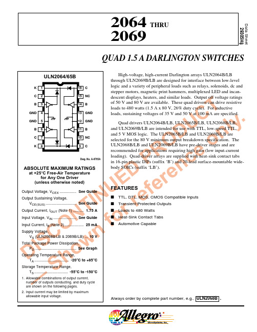
3115 Northeast Cutoff, Box 15036Worcester, Massachusetts 01615-0036 (508) 853-500042064 THRU 2069 QUAD 1.5 A DARLINGTONSWITCHES2064 THRU 2069QUAD 1.5 A DARLINGTON SWITCHES115 Northeast Cutoff, Box 15036Worcester, Massachusetts 01615-0036 (508) 853-500082064 THRU 2069QUAD 1.5 A DARLINGTONSWITCHES9ULN2064B, ULN2065B, ULN2068B, and ULN2069BDimensions in Inches (controlling dimensions)Dimensions in Millimeters(for reference only)NOTES:1.Exact body and lead configuration at vendor ’s option within limits shown.2.Lead spacing tolerance is non-cumulative.3.Lead thickness is measured at seating plane or below.4.Webbed lead frame. Leads 4, 5, 12, and 13 are internally one piece.5.Supplied in standard sticks/tubes of 25 devices.Dwg. MA-001-17A mm1618Dwg. MA-001-17A in16182064 THRU 2069QUAD 1.5 A DARLINGTON SWITCHES115 Northeast Cutoff, Box 15036Worcester, Massachusetts 01615-0036 (508) 853-500010Dwg. MA-008-21A mm1.27BSCNOTE 1NOTE 3ULN2064LB, ULN2065LB, ULN2068LB, and ULN2069LB(add “TR” to part number for tape and reel)Dimensions in Inches (for reference only)Dimensions in Millimeters (controlling dimensions)NOTES:1.Exact body and lead configuration at vendor ’s option within limits shown.2.Lead spacing tolerance is non-cumulative.3.Webbed lead frame. Leads 4 through 7 and 14 through 17 are internally one piece.4.Lead thickness is measured at seating plane or below.5.Supplied in standard sticks/tubes of 37 devices or add “TR ” to part number for tape and reel.Dwg. MA-008-21A inBSCNOTE 1NOTE 32064 THRU 2069QUAD 1.5 A DARLINGTON SWITCHES 11The products described here are manufactured under one or moreU.S. patents or U.S. patents pending.Allegro MicroSystems, Inc. reserves the right to make, from time totime, such departures from the detail specifications as may be requiredto permit improvements in the performance, reliability, ormanufacturability of its products. Before placing an order, the user iscautioned to verify that the information being relied upon is current.Allegro products are not authorized for use as critical componentsin life-support devices or systems without express written approval.The information included herein is believed to be accurate andreliable. However, Allegro MicroSystems, Inc. assumes no responsi-bility for its use; nor for any infringement of patents or other rights ofthird parties which may result from its use.2064 THRU 2069QUAD 1.5 A DARLINGTON SWITCHES115 Northeast Cutoff, Box 15036Worcester, Massachusetts 01615-0036 (508) 853-500012POWER SINK DRIVERS IN ORDER OF 1) OUTPUT CURRENT, 2) OUTPUT VOLTAGE, 3) NUMBER OF DRIVERSOutput Ratings *Features Serial Latched Diode Internal mA V #Input Drivers Clamp Outputs Protection Part Number †75178X X –constant current –62751716X X –constant current –627610020 8–––saturated –25953032X X –––58334032X X –saturated –583250 8addressable decoder/driver DMOS –6B25950 8–X –DMOS –6B27350 8X X –DMOS –6B595120248X X –constant current –627725050 8addressable decoder/driver DMOS –625950 8–X –DMOS –627350 8X X –DMOS –659550 8––X saturated –259660 4––X saturated X 255735050 4–X X ––580050 7––X ––200350 7––X ––200450 8––X ––280350 8–X X ––580150 8X X –––582150 8X X X ––584150 8addressable decoder/driver DMOS –6A25950 8X X –DMOS –6A59580 8X X –––582280 8X X X ––584295 7––X ––202395 7––X ––20244503028dual 4- to 14-line decoder/driver ––681760060 4–––saturated X 254760 4––X saturated X 2549 and 255970060 4––X saturated X 254375050 8––X saturated –2597100046 4stepper motor controller/driver MOS –7024 and 7029120046 4microstepping controller/driver MOS –7042125050 4stepper motor translator/driver –X 5804180050 4––X ––2540300046 4stepper motor controller/driver MOS –702646 4microstepping controller/driver MOS –7044400050 4––X ––2878 *Current is maximum specified test condition, voltage is maximum rating. See specification for sustaining voltage limits or over-current protection voltage limits. †Complete part number includes additional characters to indicate operating temperature range and package style.。
TA2024B中文资料
TA2024B中⽂资料TA2024BSTEREO 15W (4?) CLASS-T? DIGITAL AUDIO AMPLIFIER USING DIGITAL POWER PROCESSING? TECHNOLOGYT e c h n i c a l I n f o r m a t i o n R e v i s i o n 1.2 – J a n u a r y 2006G E N E R A L D E S C R I P T I O NThe TA2024B is a 15W/ch continuous average two-channel Class-T Digital Audio Power Amplifier IC using Tripath’s proprietary Digital Power Processing? technology. Class-T amplifiers offer both the audio fidelity of Class-AB and the power efficiency of Class-D amplifiers.A P P L I C A T I O N SComputer/PC Multimedia DVD PlayersCable Set-Top Products TelevisionsVideo CD PlayersBattery Powered SystemsB E N E F I T SFully integrated solution with FETs Easier to design-in than Class-DReduced system cost with no heat sinkDramatically improves efficiency versus Class-ABSignal fidelity equal to high quality linearamplifiersHigh dynamic range compatible with digitalmedia such as CD, DVD, and Internet audioF E A T U R E SClass-T architecture Single Supply Operation “Audiophile” Quality Sound0.03% THD+N @ 9W, 4? 0.10% IHF-IM @ 1W, 4? 11W @ 4?, 0.1% THD+N 6W @ 8?, 0.1% THD+N High Power15W @ 4?, 10% THD+N 10W @ 8?, 10% THD+N High Efficiency81% @ 15W, 4? 90% @ 10W, 8? Dynamic Range = 98 dB Mute and Sleep inputsTurn-on & turn-off pop suppression Over-current protectionOver-temperature protection Bridged outputs36-pin Power SOP packageA B S O L U T E M A X I M U M R A T I N G S (Note 1)TYPICAL PERFORMANCENote 1: Absolute Maximum Ratings indicate limits beyond which damage to the device may occur. Note 2: See Power Dissipation Derating in the Applications Information section.O P E R A T I N G C O N D I T I O N S(Note 4)Note 3: Recommended Operating Conditions indicate conditions for which the device is functional. See Electrical Characteristics for guaranteed specific performance limits.T H E R M A L C H A R A C T E R I S T I C SE L E C T R I C A L C H A R A C T E R I S T I C SSee Test/Application Circuit. Unless otherwise specified, V DD = 12V, f = 1kHz, Measurement Bandwidth = 22kHz, R L = 4?, T A = 25 °C, Package heat slug soldered to 2.8 square-inch PC pad.Note: Minimum and maximum limits are guaranteed but may not be 100% tested.P I N D E S C R I P T I O NT A 2024B P I N O U TFAULTPGND2NC NC VDD2OUTM2OUTM1VDD1NC VDDA NC PGND1CPUMP DCAP2AGND3BIASCAP INV2OAOUT2MUTE INV1OAOUT1V5A AGND2OVERLOADBREF AGND1V5DDCAP136-pin Power SOP Package(Top View)+5VGEN OUTP1VDD1VDD2OUTP2DGND NC SLEEPPin Function Description2, 3DCAP2, DCAP1Charge pump switching pins. DCAP1 (pin 3) is a free running 300kHz square wave between VDDA and DGND (12Vpp nominal). DCAP2 (pin 2) is level shifted 10 volts above DCAP1 (pin 3) with the same amplitude (12Vpp nominal), frequency, and phase as DCAP1. 4, 9 V5D, V5A Digital 5VDC, Analog 5VDC 5, 8, 17 AGND1, AGND2,AGND3 Analog Ground6 REFInternal reference voltage; approximately 1.0 VDC.7 OVERLOADB A logic low output indicates the input signal has overloaded the amplifier. 10, 14 OAOUT1, OAOUT2Input stage output pins.11, 15 INV1, INV2Single-ended inputs. Inputs are a “virtual” ground of an inverting opamp with approximately 2.4VDC bias.12 MUTE When set to logic high, both amplifiers are muted and in idle mode. When low (grounded), both amplifiers are fully operational. If left floating, the device stays in the mute mode. This pin should be tied to GND if not used. 16 BIASCAP Inputstage bias voltage (approximately 2.4VDC).18 SLEEP When set to logic high, device goes into low power mode. If not used, this pin should be grounded19FAULTA logic high output indicates thermal overload, or an output is shorted to ground, or another output.20, 35 PGND2, PGND1 Power Grounds (high current)22 DGND Digital Ground. Connect to AGND locally (near the TA2024B). 24, 27; 31, 28 OUTP2 & OUTM2; OUTP1 & OUTM1 Bridged output pairs25, 26, 29, 30 VDD2, VDD2 VDD1, VDD1 Supply pins for high current H-bridges, nominally 12VDC. 13, 21, 23, 32, 34NC Not connected. Not bonded internally. 33 VDDA Analog 12VDC 36 CPUMP Charge pump output (nominally 10V above VDDA) 1 5VGEN Regulated 5VDC source used to supply power to the input section (pins 4 and 9).A P P L I C A T I O N /T E S T C I R C U I TAll Diodes Motorola MBRS130T3* Use C o = 0.22µF for 8 Ohm loadsNote: Analog and Digital/Power Grounds must be connected locally at the TA2024BAnalog Ground Digital/Power GroundE X T E R N A L C O M P O N E N T S D E S C R I P T I O N(Refer to the Application/Test Circuit)T Y P I C A L P E R F O R M A N C EA P P L I C A T I O N I N F O R M A T I O NL a y o u t R e c o m m e n d a t i o n sThe TA2024B is a power (high current) amplifier that operates at relatively high switchingfrequencies. The outputs of the amplifier switch between the supply voltage and ground at high speeds while driving high currents. This high-frequency digital signal is passed through an LC low-pass filter to recover the amplified audio signal. Since the amplifier must drive the inductive LC output filter and speaker loads, the amplifier outputs can be pulled above the supply voltage and below ground by the energy in the output inductance. To avoid subjecting the TA2024B to potentially damaging voltage stress, it is critical to have a good printed circuit board layout. It is recommended that Tripath’s layout and application circuit be used for all applications and only be deviated from after careful analysis of the effects of any changes. Please contact TripathTechnology for further information regarding reference design material regarding the TA2024B.O u t p u t S t a g e l a y o u t C o n s i d e r a t i o n s a n d C o m p o n e n t S e l e c t i o n C r i t e r i a Proper PCB layout and component selection is a major step in designing a reliable TA2024Bpower amplifier. The supply pins require proper decoupling with correctly chosen components to achieve optimal reliability. The output pins need proper protection to keep the outputs from going below ground.The above layout shows ideal component placement and routing for channel 1 (the same design criteria applies to channel 2). This shows that C3, a 0.1uF surface mount 0805 capacitor, should be the first component placed and must decouple VDD1 (pins 29 and 30) directly to PGND1(pin35). C2, a low ESR, electrolytic capacitor, should also decouple VDD1 directly to PGND1.Both C2 and C3 may decouple VDD1 to a ground plane, but it is critical that the return path to the PGND1 pin of theTA2024B, whether it is a ground plane or a trace, be a short and direct low impedance path. Effectively decoupling VDD will shunt any power supply trace length inductance.The diodes and inductors shown are for channel 1’s outputs. D1 and L2 connect to the OUTP1 pin and D2 and L3 connect to the OUTM1 pin of the TA2024B. Each output must have a Schottky or Ultra Fast Recovery diode placed near the TA2024B, preferably immediately after thedecoupling capacitors and use short returns to PGND1. These low side diodes, D1 and D2, will prevent the outputs from going below ground. To be optimally effective they must have a short and direct return path to its proper ground pin (PGND1) of the TA2024B. This can be achieved with a ground plane or a trace.The output inductors, L2 and L3, should be placed close to the TA2024B without compromising the locations of the closely placed supply decoupling capacitors and output diodes. The purposeof placing the output inductors close to the TA2024B output pins is to reduce the trace length of the switching outputs. This will aid in reducing radiated emissions.Please see the External Component Description section on page 6 for more details on the above-mentioned components. The Application/ Test Circuit refers to the low side diodes as D O , The high side diodes as D H , and both supply decoupling capacitors as C SW .T A 2024B A m p l i f i e r G a i nThe ideal gain of the TA2024B is set by the ratio of two external resistors, R I and R F , and is given by the following formula: IF I O R R12V V ?=where V I is the input signal level and V O is the differential output signal level across the speaker. Please note that V O is 180° out of phase with V I .The ideal gain of the TA2024B is 12V/V, whereas typical values are: A V = 11.5V/V for 4? and 11.7V/V for 8?.P r o t e c t i o n C i r c u i t sThe TA2024B is guarded against over-temperature and over-current conditions. When thedevice goes into an over-temperature or over-current state, the FAULT pin goes to a logic HIGH state indicating a fault condition. When this occurs, the amplifier is muted, all outputs are TRI-STATED, and will float to 1/2 of V DD .O v e r -t e m p e r a t u r e P r o t e c t i o nAn over-temperature fault occurs if the junction temperature of the part exceeds approximately 155°C. The thermal hysteresis of the part is approximately 45°C, therefore the fault will automatically clear when the junction temperature drops below 110°C.O v e r -c u r r e n t P r o t e c t i o nAn over-current fault occurs if more than approximately 7 amps of current flows from any of the amplifier output pins. This can occur if the speaker wires are shorted together or if one side of the speaker is shorted to ground. An over-current fault sets aninternal latch that can only be cleared if the MUTE pin is toggled or if the part is powered down. Alternately, if the MUTE pin is connected to the FAULT pin, the HIGH output of the FAULT pin will toggle the MUTE pin and automatically reset the fault condition.O v e r l o a dThe OVERLOADB pin is a 5V logic output. When low, it indicates that the level of the input signal has overloaded the amplifier resulting in increased distortion at the output. The OVERLOADB signal can be used to control a distortion indicator light or LED through a simple buffer circuit, as the OVERLOADB cannot drive an LED directly.S l e e p P i nThe SLEEP pin is a 5V logic input that when pulled high (>3.5V) puts the part into a low quiescent current mode. This pin is internally clamped by a zener diode to approximately 6V thus allowing the pin to be pulled up through a large valued resistor (1meg ? recommended) to V DD . To disable SLEEP mode, the sleep pin should be grounded.F a u l t P i nThe FAULT pin is a 5V logic output that indicates various fault conditions within the device.These conditions include: low supply voltage, low charge pump voltage, low 5V regulator voltage, over current at any output, and junction temperature greater than approximately 155°C. All faults except overcurrent all reset upon removal of the condition. The FAULT output is capable of directly driving an LED through a series 2k ? resistor. If the FAULT pin is connected directly to the MUTE input an automatic reset will occur in the event of an over-current condition.P o w e r D i s s i p a t i o n D e r a t i n gFor operating at ambient temperatures above 25°C the device must be derated based on a 150°C maximum junction temperature, TJMAX as given by the following equation:JAA JMAXDISS )T T (P θ?=where…PDISS = maximum power dissipationTJMAX = maximum junction temperature of TA2024B TA = operating ambient temperatureθJA = junction-to-ambient thermal resistance Where θJA of the package is determined from the following graph:In the above graph Copper Area is the size of the copper pad on the PC board to which the heat slug of the TA2024B is soldered. The heat slug must be soldered to the PC Board to increase the maximum power dissipation capability of theTA2024B package. Soldering will minimize the likelihood of an over-temperature fault occurring during continuous heavy load conditions. The vias used for connecting the heatslug to the copper area on the PCB should be 0.013” diameter.P e r f o r m a n c e M e a s u r e m e n t s o f t h e T A 2024BThe TA2024B operates by generating a high frequency switching signal based on the audio input. This signal is sent through a low-pass filter (external to the Tripath amplifier) that recovers an amplified version of the audio input . The frequency of the switching pattern is spread spectrum and typically varies between 100kHz and 1.0MHz, which is well above the 20Hz –20kHz audio band. The pattern itself does not alter or distort the audio input signal but it does introduce some inaudible components.J AThe measurements of certain performance parameters, particularly noise related specifications such as THD+N, are significantly affected by the design of the low-pass filter used on the output as well as the bandwidth setting of the measurement instrument used. Unless the filter has a very sharp roll-off just beyond the audio band or the bandwidth of the measurement instrument is limited, some of the inaudible noise components introduced by the Tripath amplifiers switching pattern will degrade the measurement.One feature of the TA2024B is that it does not require large multi-pole filters to achieve excellent performance in listening tests, usually a more critical factor than performance measurements. Though using a multi-pole filter may remove high-frequency noise and improve THD+N type measurements (when they are made with wide-bandwidth measuring equipment), these same filters degrade frequency response. The TA2024B Evaluation Board uses the Test/Application Circuit in this data sheet, which has a simple two-pole output filter and excellent performance in listening tests. Measurements in this data sheet were taken using this same circuit with a limited bandwidth setting in the measurement instrument.P A C K A G E I N F O R M A T I O NThe package for the TA2024B is a 36-Lead Power Small Outline Package (PSOP), similar to JEDEC outline MO-166, variation AE. Tripath currently has two suppliers for this package. We recommend that the exposed copper heatslug width for the PCB design be at least 7.3mm wide to accommodate the heatslug width variation for each package. Package dimensions are based on millimeters. Measurements in inches are provided as reference only.Outline and mechanical data for PSOP36DIM MIN MAX DIM MIN MAXBSCE1 11.00A - 3.600A1 0.100 - E2 - 2.900 A2 3.000 3.300 E3 6.300 7.300 A3 0.025 0.152 E4 2.700 2.900BSC E5 - 1.000D 15.90D1 9.000 13.000 L 0.800 1.100REF D2 - 1.100 L1 1.60D3 - 1.000 L2 0.350BSCE 14.200 BSC All DIM measured in mmThis is a product in development. Tripath Technology, Inc. reserves the right to make any changes without further notice to improve reliability, function and design.Tripath and Digital Power Processing are trademarks of Tripath Technology. Other trademarks referenced in this document are owned by their respective companies.Tripath Technology, Inc. reserves the right to make changes without further notice to any products herein to improve reliability, function or design. Tripath does not assume any liability arising out of the application of use of any product or circuit described herein; neither does it convey any license under its patent rights nor the rights of others.TRIPATH’S PRODUCT ARE NOT AUTHORIZED FOR USE AS CRITICAL COMPONENTS IN LIFESUPPORT DEVICES OR SYSTEMS WITHOUT THE EXPRESS WRITTEN CONSENT OF THEPRESIDENT OF TRIPATH TECHONOLOGY, INC.As used herein:1. Life support devices or systems are devices or systems which, (a) are intended for surgical implantinto the body, or (b) support or sustain life, and whose failure to perform, when properly used inaccordance with instructions for use provided in this labeling, can be reasonably expected to resultin significant injury of the user.2. A critical component is any component of a life support device or system whose failure to performcan be reasonably expected to cause the failure of the life support device or system, or to affect itssafety or effectiveness.C o n t a c t I n f o r m a t i o nT R I P A T H T E C H N O L O G Y,I N C2560 Orchard Parkway, San Jose, CA 95131408.750.3000 - P408.750.3001 - FFor more Sales Information, please visit us @ /doc/7caf2e651eb91a37f1115cf3.html /cont_s.htm For more Technical Information, please visit us @ /doc/7caf2e651eb91a37f1115cf3.html /data.htm。
NUF2042XV6中文资料

CIRCUIT DESCRIPTION
D1(0) 6
VBUS 5
D2(0) 4
RS
C1
C1
RS
1 D1(i)
2 GND
3 D2(i)
6 1
SOT−563 CASE 463A
MARKING DIAGRAM
xx M G G
1 xx = Specific Device Code
−
10 100
−
30
36
NUF2042XV6T1
5.25 5.6 6.8 8.0
−
10 100 37.6 42 56.4
1. Measured between pins 1, 3, 4, 6 and ground with pin 5 also grounded. 2. For other resistance value (e.g. 33 W), please contact your local ON Semiconductor sales representative.
E 1.10 1.20 1.30 0.043 0.047 0.051
e
0.5 BSC
0.02 BSC
L 0.10 0.20 0.30 0.004 0.008 0.012
HE 1.50 1.60 1.70 0.059 0.062 0.066
SOLDERING FOOTPRINT*
0.3 0.0118
1.35 0.0531
Implementation because the Small IC minimizes Parasitic Inductances
Typical Applications:
• USB Hubs • Computer Peripherals Using USB
ULN2070B中文资料

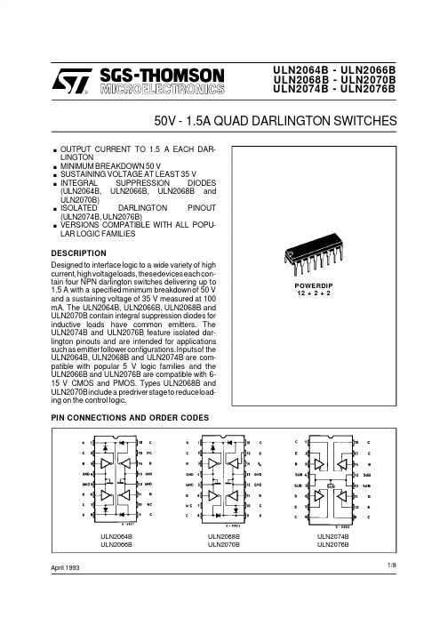
ULN2064B -ULN2066B ULN2074B -ULN2076BULN2068B -ULN2070B April 199350V -1.5A QUAD DARLINGTON SWITCHES.OUTPUT CURRENT TO 1.5A EACH DAR-LINGTON.MINIMUM BREAKDOWN 50V.SUSTAINING VOLTAGE AT LEAST 35V .INTEGRAL SUPPRESSION DIODES (ULN2064B,ULN2066B,ULN2068B and ULN2070B).ISOLATED DARLINGTON PINOUT (ULN2074B,ULN2076B).VERSIONS COMPATIBLE WITH ALL POPU-LAR LOGIC FAMILIESPOWERDIP 12+2+2PIN CONNECTIONS AND ORDER CODESULN2064B ULN2066B ULN2068B ULN2070B ULN2074B ULN2076BDESCRIPTIONDesigned to interface logic to a wide variety of high current,highvoltageloads,thesedeviceseachcon-tain four NPN darlington switches delivering up to 1.5A with a specified minimum breakdown of 50V and a sustaining voltage of 35V measured at 100mA.The ULN2064B,ULN2066B,ULN2068B and ULN2070B contain integral suppression diodes for inductive loads have common emitters.The ULN2074B and ULN2076B feature isolated dar-lington pinouts and are intended for applications suchas emitter followerconfigurations.Inputsof the ULN2064B,ULN2068B and ULN2074B are com-patible with popular 5V logic families and the ULN2066B and ULN2076B are compatible with 6-15V CMOS and PMOS.Types ULN2068B and ULN2070Binclude a predriverstageto reduceload-ing on the control logic.1/8SCHEMATIC DIAGRAMULN2064B:R IN=350ΩULN2066B:R IN=3kΩULN2068B:R IN=2.5kΩ,R s=900ΩULN2070B:R IN=11.6kΩ,R s=3.4kΩULN2074B:R IN=350ΩULN2076B:R IN=3kΩABSOLUTE MAXIMUM RATINGSSymbol Parameter Value Unit V CEX Output Voltage50V V CE(sus)Output Sustaining Voltage35VI O Output Current 1.75AV i Input Voltage for ULN2066B–2070B-2074B-2076Bfor ULN2064B–2068B 3015VVI I Input Current25mAV s Supply Voltage for ULN2068Bfor ULN2070B 1020VVP tot Power Dissipation at T pins=90°Cat T amb=70°C 4.31WWT amb Operating Ambient Temperature Range–20to85°C T stg Storage Temperature–55to150°CELECTRICAL CHARACTERISTICS(T amb=25o C unless otherwise specified)Symbol Parameter Test Conditions Min.Typ.Max.Unit Fig.I CEX Output Leakage Current V CE=50VT amb=25°CT amb=70°C 100500µAµA1V CE(sus)Collector-emitter Sustaining Voltage I C=100mA,V i=0.4V35V2V CE(sat)Collector-emitter Saturation Voltage I C=500mA I B=625µAI C=750mA I B=935µAI C=1A I B=1.25mAI C=1.25A I B=2mA 1.11.21.31.4VVVV3333I i(on)Input Current for ULN2064B and ULN2074BV i=2.4VV i=3.75Vfor ULN2066B and ULN2076BV i=5VV i=12Vfor ULN2068BV i=2.75VV i=3.75Vfor ULN2070BV i=5VV i=12V 1.43.30.61.74.39.61.85.20.551.00.41.25mAmAmAmAmAmAmAmA44444444ULN2064B-ULN2066B-ULN2068B-ULN2070B-ULN2074B-ULN2076B 2/8ELECTRICAL CHARACTERISTICS(T amb=25o C unless otherwise specified)(continued)Symbol Parameter Test Conditions Min.Typ.Max.Unit Fig.V i(on)Input Voltage V CE=2V,I C=1AULN2064B,ULN2074BULN2066B,ULN2076BV CE=2V,I C=1.5AULN2064B,ULN2074BULN2066B,ULN2076BULN2068BULN2070B26.52.5102.755VVVVVV555555I s Supply Current for ULN2068BI C=500mA,V i=2.75Vfor ULN2070BI C=500mA,V i=5V64.5mAmA88t PLH Turn-on Delay Time0.5V i to0.5V o1µs t PHL Turn-off Delay Time0.5V i to0.5V o 1.5µs I R Clamp Diode Leakage Current for ULN2064B-ULN2066Band ULN2068B-ULN2070BV R=50VT amb=25°CT amb=70°C 50100µAµA6V F Clamp Diode Forward Voltage for ULN2064B-ULN2066Band ULN2068B-ULN2070B I F=1AI F=1.5A 1.752VV7No tes: 1.Input voltage is with reference to the substrate(no connection to any other pins)for the ULN2074B and ULN2076B reference is ground for all other types.2.Input current may be limited by maximum allowable input voltage.TEST CIRCUITSFigure1.Figure2.Figure3.Figure4.ULN2064B-ULN2066B-ULN2068B-ULN2070B-ULN2074B-ULN2076B3/8Figure5.Figure6. Figure7.Figure8.Figure9:Input Current as a Function ofInput Voltage.Figure10:Input Current as a Function ofInput Voltage.Figure11:CollectorCurrent as a Function ofInput Current.ULN2064B-ULN2066B-ULN2068B-ULN2070B-ULN2074B-ULN2076B 4/8MOUNTING INSTRUCTIONSThe R th j-amb can be reduced by soldering the GND pins to a suitable copper area of the printed circuit board(Fig.12)or to an external heatsink(Fig.13). The diagram of Figure14shows the maximum dis-sipable power P tot and the R th j-amb as a function of the side”α”of two equal square copper areas hav-ing a thickness of35µ(1.4mils).During soldering the pins temperature must not ex-ceed260°C and the soldering time must not be longer than12seconds.The external heatsink or printed circuit copper area must be connected to electrical ground.Figure12:Example of P.C.Board Area which isUsed as Heatsink.Figure13:ExternalHeatsink Mounting Example.Figure14:Maximum Dissipable Power and Junc-tion to Ambient Thermal Resistancevs.Side”α”.Figure15:Maximum Allowable Power Dissipa-tion vs.Ambient Temperature.ULN2064B-ULN2066B-ULN2068B-ULN2070B-ULN2074B-ULN2076B5/8ULN2064B-ULN2066B-ULN2068B-ULN2070B-ULN2074B-ULN2076BTYPICAL APPLICATIONSFigure16:Common-anode LED Drivers.Figure17:Common-cathode LED Drivers. 6/8ULN2064B-ULN2066B-ULN2068B-ULN2070B-ULN2074B-ULN2076B POWERDIP16PACKAGE MECHANICAL DATAmm inch DIM.MIN.TYP.MAX.MIN.TYP.MAX.a10.510.020B0.85 1.400.0330.055b0.500.020b10.380.500.0150.020D20.00.787E8.800.346e 2.540.100e317.780.700F7.100.280I 5.100.201L 3.300.130Z 1.270.0507/8ULN2064B-ULN2066B-ULN2068B-ULN2070B-ULN2074B-ULN2076BInformation furnished is believed to be accurate and reliable.However,SGS-THOMSON Microelectronics assumes no responsibility for the consequence s of use of such information nor for any infringement of patents or other rights of third parties which may result from its use.No license is granted by implication or otherwise under any patent or patent rights of SGS-THOMSON Microelectronics.Specification mentioned in this publication are subject to change without notice.This publication supersedes and replaces all information previously supplied.SGS-THOMSON Microelectronics products are not authorized for use as critical components in life support devices or systems without express written approval of SGS-THOMSON Microelectronics.©1996SGS-THOMSON Microelectronics–Printed in Italy–All Rights ReservedSGS-THOMSON Microelectronics GROUP OF COMPANIESAustralia-Brazil-Canada-China-France-Germany-Hong Kong-Italy-Japan-Korea-Malaysia-Malta-Morocco-The Netherlands-Singapore-Spain-Sweden-Switzerland-Taiwan-Thailand-United Kingdom-U.S.A.8/8。
UL20(中文版)
1 范围1.1本标准的要求适用于依据“国家电气规范”(NEC),ANSI/NFPA70,或加拿大电气规范(CEC)第1部分所使用的铜或镀铜导线连接,或在NEC或CEC认可的布线系统中使用的、手动操作的、一般用途瞬动开关。
在加拿大,对于依据CEC第1部分在与铝导线连接,且在CEC第1部分认可的布线系统内谅解的开关的要求,见附录B。
1.2本标准适用于电压为250V及以下负载额定不超过60A,电压为251~600V时负载额定不超过30A,电压为125V~600V及以下时功率为2hp的交流/直流开关。
1.3本标准适用于安装在暗装式开关盒内或出线盒盖上、并用于支路布线连接的开关。
1.4本标准适用于软线现场安装并提供一个“on”和一个“off”位置的悬挂开关和开关。
1.5 本标准适用于明装式安装并带有一单独底座和盖的开关。
1.6 本标准适用于用于不带单独接线盒暗装式安装和连接支路布线(由一个或多个非金属铠装且为黄铜导线的电缆构成)的开关。
1.7 此标准适用于应用在固定装置中以控制支路配线中的白炽灯照明或风扇交流/直流固定装置开关。
1.8此标准适用于单极、瞬间接触门开关(用于安装在特殊用途装置盒内或连接支路接线连接用出线盒盖上)。
1.9此标准不适用于:a)UL 917--钟控开关和CSA 标准C22.2 No.177中规定的钟控开关;b)UL 1472—固体调光控制器和CSA标准C22.2 No.184.1中规定的调光开关;c)UL 508—工业控制设备和CSA标准C22.2 No.14中规定的工业控制设备;d)UL 1917—固态风速控制器和CSA标准C22.2 No.156中规定的固体、单相马达速度控制器;e)UL 1054—专用开关和CSA标准C22.2 No.55中规定的专用和交流固定装置开关;f)UL 894—危险场所用开关和CSA标准C22.2 No.159中规定的在危险场所中使用的开关。
1.10对于在支路配线连接的开关(支路铝配线),请参考UL 1567—铝线用插座和开关或参考附录B。
B201220600中文资料
Power supply DC type Rated operational voltage 024 Rated insulபைடு நூலகம்tion voltage Rated transient protection volt. Consumption AC supply DC supply
Mode of Operation
Ordering Key
Function Output Type Power supply Time range
B 108 024 600
Type Selection
Plug Circular 8 pin Circular 11 pin Circular 8 pin Circular 11 pin DPDT Output SPDT Time ranges 0.15 - 6 s 1.5 - 60 s 15 - 600 s 0.15 - 6 s 1.5 - 60 s 15 - 600 s 0.15 - 6 s 1.5 - 60 s 15 - 600 s 0.15 - 6 s 1.5 - 60 s 15 - 600 s Supply: 24 VAC/DC B 108 024 006 B 108 024 060 B 108 024 600 B 101 024 006 B 101 024 060 B 101 024 600 B 208 024 006 B 208 024 060 B 208 024 600 B 201 024 006 B 201 024 060 B 201 024 600 Supply: 120 VAC B 108 120 006 B 108 120 060 B 108 120 600 B 101 120 006 B 101 120 060 B 101 120 600 B 208 120 006 B 208 120 060 B 208 120 600 B 201 120 006 B 201 120 060 B 201 120 600 Supply: 220 VAC B 108 220 006 B 108 220 060 B 108 220 600 B 101 220 006 B 101 220 060 B 101 220 600 B 208 220 006 B 208 220 060 B 208 220 600 B 201 220 006 B 201 220 060 B 201 220 600
BL-BYG204中文资料

DUAL-CHIP & TRI-STATE LED LAMPSChipAbsolute MaximumRatings Electro-opticalData (At 20mA)Vf (V) Iv (mcd) PackagePart No.Material/EmittedColor Peak Wave Length λp (nm) Lens Appearance∆λ (nm) Pd (mw) If (mA) Peak (mA) Typ Max Typ. ViewingAngle 2θ 1/2 (deg) DrawingNo. GaP/GaP/Bright Red 700 90 40 15 50 2.2 2.6 7.0 BL-BHG201 GaP/GaP/Yellow Green 568 White Diffused 30 80 30 150 2.2 2.6 35.0 GaAsP/GaP/Hi-Eff Red 635 45 80 30 150 2.0 2.6 35.0BL-BEG201GaP/GaP/Yellow Green 568 White Diffused 30 80 30 150 2.2 2.6 35.0 GaAsP/GaP/Yellow 585 35 80 30 150 2.1 2.6 30.0 T-1 Standard1.0″ Lead 3 φBL-BYG201 GaP/GaP/Yellow Green 568 White Diffused 30 80 30 150 2.2 2.6 35.0 40 L-070GaP/GaP/Bright Red 700 90 40 15 50 2.2 2.6 8.0 BL-BHG204GaP/GaP/Yellow Green 568 White Diffused 30 80 30 150 2.2 2.6 45.0 GaAsP/GaP/Hi-Eff Red 635 45 80 30 150 2.0 2.6 45.0BL-BEG204GaP/GaP/Yellow Green 568 White Diffused 30 80 30 150 2.2 2.6 45.0 GaAsP/GaP/Yellow 585 35 80 30 150 2.1 2.6 40.0 T-13/4 Standard1.0″ Lead 5 φBL-BYG204 GaP/GaP/Yellow Green 568 White Diffused 30 80 30 150 2.2 2.6 45.0 50 L-071GaP/GaP/Bright Red 700 90 40 15 50 2.2 2.6 3.5 BL-BHG204-AGaP/GaP/Yellow Green 568 White Diffused 30 80 30 150 2.2 2.6 20.0 GaAsP/GaP/Hi-Eff Red 635 45 80 30 150 2.0 2.6 20.0BL-BEG204-AGaP/GaP/Yellow Green 568 White Diffused 30 80 30 150 2.2 2.6 20.0 GaAsP/GaP/Yellow 585 35 80 30 150 2.1 2.6 18.0 T-13/4 Standard1.0″ Lead 5 φBL-BYG204-A GaP/GaP/Yellow Green 568 White Diffused 30 80 30 150 2.2 2.6 20.0 50 L-072GaP/GaP/Bright Red 700 90 40 15 50 2.2 2.6 3.5 BL-BHG204-B GaP/GaP/Yellow Green 568 White Diffused 30 80 30 150 2.2 2.6 20.0 GaAsP/GaP/Hi-Eff Red 635 45 80 30 150 2.0 2.6 20.0BL-BEG204-B GaP/GaP/Yellow Green 568 White Diffused 30 80 30 150 2.2 2.6 20.0 GaAsP/GaP/Yellow 585 35 80 30 150 2.1 2.6 18.0 T-13/4-Standard 1.0″ Lead 5 φBL-BYG204-BGaP/GaP/Yellow Green568White Diffused3080301502.2 2.6 20.050 L-073Remark: 1. Hi-Eff Red/High-Efficiency Red. 2. Trans/Transparent.3. 2θ 1/2 The off-axis angle at which the luminous intensity is half the axial luminous intensity. Notes: 1. All Dimensions are in millimeters (inches). 2. Tolerance is ±0.25mm (.010″)元器件交易网。
ULN2004

高压大电流达林顿晶体管阵列系列产品及其应用摘要:ULN2000、ULN2800是高压大电流达林顿晶体管阵列系列产品,具有电流增益高、工作电压高、温度范围宽、带负载能力强等特点,适应于各类要求高速大功率驱动的系统。
ULN2003A电路是美国Texas Instruments公司和Sprague公司开发的高压大电流达林顿晶体管阵列电路,文中介绍了它的电路构成、特征参数及典型应用。
关键词:达林顿晶体管阵列驱动电路ULN2003 ULN2000系列ULN2800系列1 概述功率电子电路大多要求具有大电流输出能力,以便于驱动各种类型的负载。
功率驱动电路是功率电子设备输出电路的一个重要组成部分。
在大型仪器仪表系统中,经常要用到伺服电机、步进电机、各种电磁阀、泵等驱动电压高且功率较大的器件。
ULN2000、ULN2800高压大电流达林顿晶体管阵列系列产品就属于这类可控大功率器件,由于这类器件功能强、应用范围语广。
因此,许多公司都生产高压大电流达林顿晶体管阵列产品,从而形成了各种系列产品,ULN2000、ULN2800系列就是美国Texas Instruments公司、美国Sprague公司开发的高压大电流达林顿晶体管阵列产品。
它们的系列型号分类如表1所列,生产2000、2800高压大电流达林顿晶体管阵列系列产品的公司与型号对照表如表2所列。
在上述系列产品中,ULN2000系列能够同时驱动7组高压大电流负载,ULN2800系列则能够同时驱动8组高压大电流负载。
美国Texas Instruments公司、美国Sprague公司生产的ULN2003A 由7组达林顿晶体管阵列和相应的电阻网络以及钳位二极管网络构成,具有同时驱动7组负载的能力,为单片双极型大功率高速集成电路。
以下介绍该电路的构成、性能特征、电参数以及典型应用。
2000、2800高压大电流达林顿晶体管阵列系列中的其它产品的性能特性与应用可参考ULN2003A。
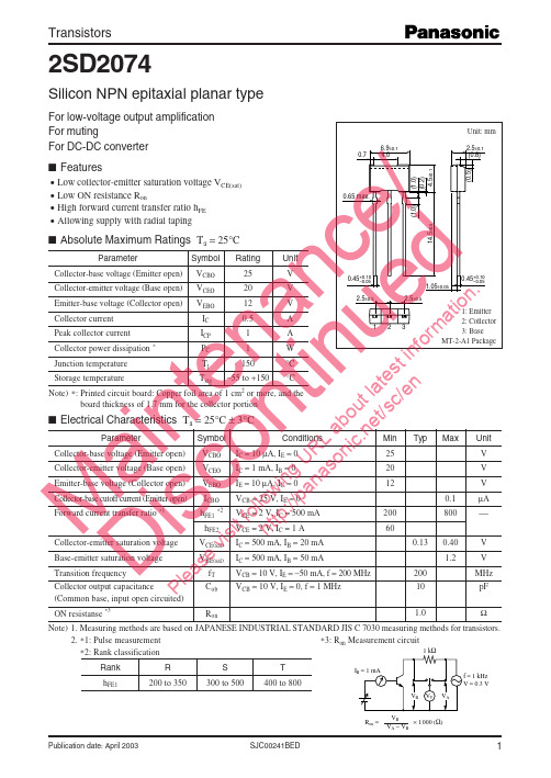
2SD2074S中文资料
2
SJC00241BED
Request for your special attention and precautions in using the technical information and semiconductors described in this book
(1) If any of the products or technical information described in this book is to be exported or provided to non-residents, the laws and regulations of the exporting country, especially, those with regard to security export control, must be observed. (2) The technical information described in this book is intended only to show the main characteristics and application circuit examples of the products, and no license is granted under any intellectual property right or other right owned by our company or any other company. Therefore, no responsibility is assumed by our company as to the infringement upon any such right owned by any other company which may arise as a result of the use of technical information described in this book. (3) The products described in this book are intended to be used for standard applications or general electronic equipment (such as office equipment, communications equipment, measuring instruments and household appliances). Consult our sales staff in advance for information on the following applications: – Special applications (such as for airplanes, aerospace, automobiles, traffic control equipment, combustion equipment, life support systems and safety devices) in which exceptional quality and reliability are required, or if the failure or malfunction of the products may directly jeopardize life or harm the human body. – Any applications other than the standard applications intended. (4) The products and product specifications described in this book are subject to change without notice for modification and/or improvement. At the final stage of your design, purchasing, or use of the products, therefore, ask for the most up-to-date Product Standards in advance to make sure that the latest specifications satisfy your requirements. (5) When designing your equipment, comply with the range of absolute maximum rating and the guaranteed operating conditions (operating power supply voltage and operating environment etc.). Especially, please be careful not to exceed the range of absolute maximum rating on the transient state, such as power-on, power-off and mode-switching. Otherwise, we will not be liable for any defect which may arise later in your equipment. Even when the products are used within the guaranteed values, take into the consideration of incidence of break down and failure mode, possible to occur to semiconductor products. Measures on the systems such as redundant design, arresting the spread of fire or preventing glitch are recommended in order to prevent physical injury, fire, social damages, for example, by using the products. (6) Comply with the instructions for use in order to prevent breakdown and characteristics change due to external factors (ESD, EOS, thermal stress and mechanical stress) at the time of handling, mounting or at customer's process. When using products for which damp-proof packing is required, satisfy the conditions, such as shelf life and the elapsed time since first opening the packages. (7) This book may be not reprinted or reproduced whether wholly or partially, without the prior written permission of Matsushita Electric Industrial Co., Ltd.
75176B中文资料

75176B中⽂资料PACKAGING INFORMATION Orderable Device Status(1)PackageType PackageDrawingPins PackageQtyEco Plan(2)Lead/Ball Finish MSL Peak Temp(3)SN65176BD ACTIVE SOIC D875Green(RoHS&no Sb/Br)CU NIPDAU Level-1-260C-UNLIMSN65176BDE4ACTIVE SOIC D875Green(RoHS&no Sb/Br)CU NIPDAU Level-1-260C-UNLIMSN65176BDG4ACTIVE SOIC D875Green(RoHS&no Sb/Br)CU NIPDAU Level-1-260C-UNLIMSN65176BDR ACTIVE SOIC D82500Green(RoHS& no Sb/Br)CU NIPDAU Level-1-260C-UNLIMSN65176BDRE4ACTIVE SOIC D82500Green(RoHS& no Sb/Br)CU NIPDAU Level-1-260C-UNLIMSN65176BDRG4ACTIVE SOIC D82500Green(RoHS& no Sb/Br)CU NIPDAU Level-1-260C-UNLIMSN65176BP ACTIVE PDIP P850Pb-Free (RoHS)CU NIPDAU N/A for Pkg TypeSN65176BPE4ACTIVE PDIP P850Pb-Free (RoHS)CU NIPDAU N/A for Pkg TypeSN75176BD ACTIVE SOIC D875Green(RoHS&no Sb/Br)CU NIPDAU Level-1-260C-UNLIMSN75176BDE4ACTIVE SOIC D875Green(RoHS&no Sb/Br)CU NIPDAU Level-1-260C-UNLIMSN75176BDG4ACTIVE SOIC D875Green(RoHS&no Sb/Br)CU NIPDAU Level-1-260C-UNLIMSN75176BDR ACTIVE SOIC D82500Green(RoHS& no Sb/Br)CU NIPDAU Level-1-260C-UNLIMSN75176BDRE4ACTIVE SOIC D82500Green(RoHS&no Sb/Br)CU NIPDAU Level-1-260C-UNLIMSN75176BDRG4ACTIVE SOIC D82500Green(RoHS&no Sb/Br)CU NIPDAU Level-1-260C-UNLIMSN75176BP ACTIVE PDIP P850Pb-Free(RoHS)CU NIPDAU N/A for Pkg TypeSN75176BPE4ACTIVE PDIP P850Pb-Free(RoHS)CU NIPDAU N/A for Pkg TypeSN75176BPSR ACTIVE SO PS82000Green(RoHS&no Sb/Br)CU NIPDAU Level-1-260C-UNLIMSN75176BPSRG4ACTIVE SO PS82000Green(RoHS&no Sb/Br)CU NIPDAU Level-1-260C-UNLIM(1)The marketing status values are defined as follows:ACTIVE:Product device recommended for new designs.LIFEBUY:TI has announced that the device will be discontinued,and a lifetime-buy period is in effect.NRND:Not recommended for new designs.Device is in production to support existing customers,but TI does not recommend using this part in a new design.PREVIEW:Device has been announced but is not in production.Samples may or may not be available.OBSOLETE:TI has discontinued the production of the device.(2)Eco Plan-The planned eco-friendly classification:Pb-Free(RoHS),Pb-Free(RoHS Exempt),or Green(RoHS&no Sb/Br)-please check /doc/7167b986cc22bcd126ff0c93.html /productcontent for the latest availability information and additional product content details.TBD:The Pb-Free/Green conversion plan has not been defined.Pb-Free(RoHS):TI's terms"Lead-Free"or"Pb-Free"mean semiconductor products that are compatible with the current RoHS requirements for all6substances,including the requirement that lead not exceed0.1%by weight in homogeneous materials.Where designed to be soldered at high temperatures,TI Pb-Free products are suitable for use in specified lead-free processes.Pb-Free(RoHS Exempt):This component has a RoHS exemption for either1)lead-based flip-chip solder bumps used between the die andpackage,or2)lead-based die adhesive used between the die and leadframe.The component is otherwise considered Pb-Free(RoHS compatible)as defined above.Green(RoHS&no Sb/Br):TI defines"Green"to mean Pb-Free(RoHS compatible),and free of Bromine(Br)and Antimony(Sb)based flame retardants(Br or Sb do not exceed0.1%by weight in homogeneous material)(3)MSL,Peak Temp.--The Moisture Sensitivity Level rating according to the JEDEC industry standard classifications,and peak soldertemperature.Important Information and Disclaimer:The information provided on this page represents TI's knowledge and belief as of the date that it is provided.TI bases its knowledge and belief on information provided by third parties,and makes no representation or warranty as to the accuracy of such information.Efforts are underway to better integrate information from third parties.TI has taken and continues to take reasonable steps to provide representative and accurate information but may not have conducted destructive testing or chemical analysis on incoming materials and chemicals.TI and TI suppliers consider certain information to be proprietary,and thus CAS numbers and other limited information may not be available for release.In no event shall TI's liability arising out of such information exceed the total purchase price of the TI part(s)at issue in this document sold by TI to Customer on an annual basis.TAPE AND REEL INFORMATIONDevice Package Pins Site ReelDiameter(mm)ReelWidth(mm)A0(mm)B0(mm)K0(mm)P1(mm)W(mm)Pin1QuadrantSN65176BDR D8FMX33012 6.4 5.2 2.1812Q1 SN75176BDR D8FMX33012 6.4 5.2 2.1812Q1 SN75176BPSR PS8MLA330168.2 6.6 2.51216Q1TAPE AND REEL BOX INFORMATIONDevice Package Pins Site Length(mm)Width(mm)Height(mm)SN65176BDR D8FMX338.1340.520.64SN75176BDR D8FMX338.1340.520.64SN75176BPSR PS8MLA342.9336.628.58。
ULN2064B中文资料
tPHL Turn-off Delay Time
0.5 Vi to 0.5 Vo
1.5 µs
IR Clamp Diode Leakage Current
for ULN2064B-ULN2066B and ULN2068B-ULN2070B VR = 50 V
Tamb = 25°C Tamb = 70°C
IC = 100mA, Vi = 0.4V
IC = 500mA
IC = 750mA IC = 1A IC = 1.25A
IB = 625µA
IB = 935µA IB = 1.25mA IB = 2mA
for ULN2064B and ULN2074B
Vi = 2.4V Vi = 3.75V for ULN2066B and ULN2076B
Value
Unit
50
V
35
V
1.75
A
30
V
15
V
25
mA
10
V
20
V
4.3
W
1
W
– 20 to 85
°C
– 55 to 150
°C
ELECTRICAL CHARACTERISTICS (Tamb = 25oC unless otherwise specified )
Symbol ICEX
VCE(sus) VCE(sat)
4/8
元器件交易网
ULN2064B-ULN2066B-ULN2068B-ULN2070B-ULN2074B-ULN2076B
MOUNTING INSTRUCTIONS
The Rth j-amb can be reduced by soldering the GND pins to a suitable copper area of the printed circuit board (Fig. 12) or to an external heatsink (Fig. 13).
269-B中文资料

269-Type 14xx nm Pump Laser Module with Fiber Grating Data Sheet June 2001Offering superior wavelength stability, the 269-type pump laser module with fiber grating is designed as a continuous-wave (CW) optical pump source for erbium-doped fiber ampli-fiers and Raman pump modules.Featuress High-coupled rated output power up to 280 mW, CWs Available with fiber grating for wavelength stability (1420 nm—1510 nm)s Wide environmental ranges Field-proven packaging technologys InGaAsP/InP high-power, strained multiple quan-tum-well (MQW) chip designs Internal thermoelectric cooler (TEC)s InGaAs PIN photodetector back-facet monitors Single-mode and polarization-maintaining fiber pig-tailss Compact, 14-pin butterfly packages Industry compatible package and pinout Applicationss Raman pump modules (RPM)s Erbium-doped fiber amplifiers (EDFA) DescriptionThe 269-type pump laser module with fiber grating represents a family of thermoelectrically cooled, high-power lasers. These modules utilize a fiber Bragg grating to achieve stable wavelength perfor-mance within the 1420 nm to 1510 nm range, over the full operating temperature range. They are designed as continuous-wave (CW) optical pump sources for dense wavelength-division multiplexing (DWDM) EDFA and Raman applications operating in the C- and L-bands. The 269-type laser modules with polarization-maintaining fiber are particularly suitable for use in RPM designs requiring the high-power combinations of multiple pumps.The laser optical spectrum is locked by the fiber grat-ing over a wide optical power range. The optical spectrum is very narrow and the peak wavelength is nearly insensitive to temperature variations and back reflections.The laser modules incorporate a high-power, quan-tum-well laser chip that achieves grating-stabilized fiber powers ranging to 280 mW.An integral thermoelectric cooler (TEC) stabilizes the laser at room temperature and, combined with a her-metic environment, allows the device to achieve high-power operation over the extended temperature range of 0 °C to 75 °C. An internal InGaAs PIN pho-todiode, mounted behind the laser diode, functions as the laser detector and monitors light emissions from the rear facet of the laser.The 269-type module is offered in a 14-pin, hermetic butterfly package.269-Type 14xx nm Pump Laser Module Data Sheet with Fiber GratingJune 20012Agere Systems Inc.Absolute Maximum RatingsStresses in excess of the absolute maximum ratings can cause permanent damage to the device. These are abso-lute stress ratings only. Functional operation of the device is not implied at these or any other conditions in excess of those given in the operational sections of the data sheet. Exposure to absolute maximum ratings for extended periods can adversely affect device reliability.Handling PrecautionsElectrostatic DischargeCAUTION: This device is susceptible to damage as a result of electrostatic discharge (ESD). Take properprecautions during both handling and testing. Follow guidelines such as EIA * Standard EIA 625.Agere Systems Inc. employs a human-body model (HBM) for ESD-susceptibility testing and protection-design eval-uation. ESD voltage thresholds are dependent on the critical parameters used to define the model. A standard HBM (resistance = 1.5 k Ω, capacitance = 100 pF) is widely used and, therefore, can be used for comparison pur-poses. The HBM ESD withstand voltage established for the 269-type laser pump module is ±500V .* EIA is a registered trademark of The Electronic Industries Association.ParameterSymbol Min Max Unit Operating Case T emperature Range T C 075°C Storage Case T emperature Range T stg –4085°C Laser Forward Bias (TEC on):P O = 120 mW—150 mW P O = 160 mW—210 mW P O = 220 mW—280 mW I F———100015001900mA mA mA Laser Reverse VoltageV R —2V Photodiode Reverse Voltage V RMON —20V TEC Current I TEC — 2.2A TEC VoltageV TEC — 5.0V T emperature Sensor CurrentI TS —5mA Laser Diode Operating Chip T emperatureT LD—40°CData Sheet 269-Type 14xx nm Pump Laser ModuleJune 2001with Fiber Grating3Agere Systems Inc.Electrical/Optical CharacteristicsTable 1. Electrical/Optical Characteristics (All performance parameters are specified for I F , OP , T SET = 25 °C,T CASE ~ 25 °C, unless otherwise specified.)ParameterSymbol ConditionsMin Typ Max Unit Operating Optical Power P O —120—280mW Wavelength:T arget Wavelength Center Wavelength λt λC —0 °C—70 °C1420λt – 1.5——1510λt + 1.5nm nm RMS Spectral Width∆λP O—— 1.5nmBOL Operating Laser Forward Current:P O = 120 mW P O = 130 mW P O = 140 mW P O = 150 mWI F , OP BOL————————————550600600600mA mA mA mABOL Operating Laser Forward Current:P O = 160 mW P O = 170 mW P O = 180 mW P O = 190 mW P O = 200 mWI F , OP BOL———————————————650700700750800mA mA mA mA mABOL Operating Laser Forward Current:P O = 210 mW P O = 220 mW P O = 230 mW P O = 240 mW P O = 250 mW P O = 260 mW P O = 270 mW P O = 280 mWI F , OP BOL————————————————————————85090095010001000110011001100mA mA mA mA mA mA mA mA EOL Operating Laser Forward Current I F , OP EOL ——— 1.15 xI F , OP BOLmA EOL Laser Diode Forward Voltage V RI F , OP EOL— 2.3 3.0V Polarization Extinction RatioPER—13——dBTable 2. Monitor Photodiode Characteristics (All test parameters are specified for I F , OP , T SET = 25 °C,T CASE ~ 25 °C unless otherwise specified.)ParameterSymbol Conditions Min Max Unit Monitor Diode CurrentI BF —2002000µA Monitor Diode Dark CurrentI DV R = –5 V , I F = 0—100nA269-Type 14xx nm Pump Laser Module Data Sheet with Fiber GratingJune 20014Agere Systems Inc.Electrical/Optical Characteristics (continued)Table 3. TEC and Thermistor Characteristics (All performance parameters are specified for I F , OP , T SET = 25 °C,unless otherwise specified.)ParameterSymbol Conditions Min Max Unit TEC Current:P O = 120 mW P O = 130 mW P O = 140 mW P O = 150 mW I TECT SET = 25 °C;T CASE = 75 °C;∆T = 50 °C, EOL———— 1.61.61.61.6A A A A TEC Current:P O = 160 mW P O = 170 mW P O = 180 mW P O = 190 mW P O = 200 mW I TECT SET = 25 °C;T CASE = 70 °C;∆T = 45 °C, EOL————— 1.71.71.71.71.7A A A A A TEC Current:P O = 210 mW P O = 220 mW P O = 230 mW P O = 240 mW P O = 250 mW P O = 260 mW P O = 270 mW P O = 280 mW I TECT SET = 25 °C;T CASE = 65 °C;∆T = 40 °C, EOL———————— 2.02.02.02.02.02.02.02.0A A A A A A A A TEC Voltage:P O = 120 mW P O = 130 mW P O = 140 mW P O = 150 mW V TECT SET = 25 °C;T CASE = 75 °C;∆T = 50 °C, EOL———— 3.53.53.53.5V V V V TEC Voltage:P O = 160 mW P O = 170 mW P O = 180 mW P O = 190 mW P O = 200 mW V TECT SET = 25 °C;T CASE = 70 °C;∆T = 45 °C, EOL————— 3.73.73.73.73.7V V V V V TEC Voltage:P O = 210 mW P O = 220 mW P O = 230 mW P O = 240 mW P O = 250 mW P O = 260 mW P O = 270 mW P O = 280 mWV TECT SET = 25 °C;T CASE = 65 °C;∆T = 40 °C, EOL———————— 4.24.24.24.24.24.24.24.2V V V V V V V V Thermistor Resistance R THERM25 °C Laser Diode Set T emperature9.510.5k ΩThemistor B ConstantB—37004100KData Sheet 269-Type 14xx nm Pump Laser ModuleJune 2001with Fiber Grating 5Agere Systems Inc.User Information*A positive input into this pin cools the laser.Fiber CharacteristicssLength of fiber pigtail:— 1.75 m ± 0.25 msLength of fiber pigtail to end of grating:— 0.86 m ± 0.14 msStandard fiber:— Cladding OD: 125 µm ± 2 µm— Acrylate buffer OD: 250 µm ± 15 µm — Cut off wavelength: <1320 nm sPolarization-maintaining fiber:— P ANDA— Cut off wavelength: <1400 nm — Acrylate buffer: 400 µmTable 4. Pin Information Pin Number Connection1TE Cooler (+)*2Thermistor3Monitor Anode (–Bias)4Monitor Cathode (+Bias)5Thermistor 6No Connect 7No Connect 8No Connect 9No Connect 10Laser Anode (+)11Laser Cathode (–)12No Connect13Package Ground 14TEC Cooler (–)Mounting and ConnectionsCAUTION:This device is susceptible to damage asa result of electrostatic discharge. Proper precautions should be taken during both handling and testing.The base of the laser module (see Outline Diagram) should be maintained at or below 75 °C (maximum) during operation. Interfaces between the laser module base and heat sink must be clean, and the use of a thermal filler may be necessary.Mounting InstructionsThe minimum fiber bend radius is 1.0 in.T o avoid degradation in performance, mount the mod-ule on the board as follows:1.Place the bottom flange of the module on a flat heat sink at least 0.5 in. x 1.180 in. (12.7 mm x 30 mm) in size. The surface finish of the heat sink should be better than 32 µin. (0.8 µm), and the surface flat-ness must be better than 0.001 in. (25.4 µm). Using thermal conductive grease is optional; however, thermal performance may be improved if conductive grease is applied between the bottom flange and the heat sink.2.Mount four #2-56 screws with Fillister heads (M2-3 mm) at the four screw hole locations (see Outline Diagram). The Fillister head diameter must not exceed 0.140 in. (3.55 mm). Do not apply more than 1 in./lb. of torque to the screws.Figure 1. Circuit Schematic1-675 (F).h7654321891011121314TH 10 k ΩTEC–++–269-Type 14xx nm Pump Laser Module Data Sheet with Fiber GratingJune 20016Agere Systems Inc.Outline DiagramDimensions are in inches and (millimeters).1-1065 (F)a0.10 (0.25)0.035(0.91)0.078(1.98)0.213 (5.40) TYP.0.350(8.89)0.500(12.70)0.598(15.19)MAX.1.025(26.04)0.020(0.51)0.100 (2.54) TYP.TYP.PIN 10.105 (2.667) DIA.TYP. (4) PLACESPIN 140.030 (0.76)0.700(17.78)0.347(8.8)0.820(20.83)0.180(4.57)0.175(4.45)0.215(5.46) 1.180(29.97)0.078(1.99)0.178(4.52)0.215 ± 0.10(5.46 ± 2.54)0.363(9.23)0.334 ± 0.005(8.49 ± 0.005)Data Sheet 269-Type 14xx nm Pump Laser ModuleJune 2001with Fiber Grating7Agere Systems Inc.Laser Safety InformationClass IIIb Laser ProductFDA/CDRH Class IIIb laser product. All versions are Class IIIb laser products per CDRH, 21 CFR 1040 Laser Safety requirements. All versions are Class IIIb laser products per IEC * 60825-1:1993. The device has been classified with the FDA under accession number 8720010.This product complies with 21 CFR 1040.10 and 1040.11.8.8 µm/125 µm single-mode fiber pigtail (see Fiber Characteristics, page 5).Wavelength = 1.40 µm—1.52 µm.Maximum power = 400 mW.Because of size constraints, laser safety labeling (including an FDA Class IIIb label) is not affixed to the module but attached to the outside of the shipping carton.Product is not shipped with power supply.Caution:Use of controls, adjustments, and procedures other than those specified herein may result inhazardous laser radiation exposure.* IEC is a registered trademark of The International Electrotechnical Commission.DANGERINVISIBLE LASER RADIATION IS EMITTED FROM THE END OF FIBER OR CONNECTOR Avoid direct exposure to beam Do not view beam directly with optical instrumentsINVISIBLE LASER RADIATION EMITTED FROM END OF FIBER OR CONNECTORAvoid exposure to beamClass 3B Laser Product IEC-60825M 1993;Max. Output: 400 mW;Wavelength: 1.40 µm—1.52 µm269-Type 14xx nm Pump Laser Module Data Sheet with Fiber GratingJune 2001For additional information, contact your Agere Systems Account Manager or the following:INTERNET: E-MAIL:docmaster@ N. AMERICA:Agere Systems Inc., 555 Union Boulevard, Room 30L-15P-BA, Allentown, P A 18109-32861-800-372-2447, FAX 610-712-4106 (In CANADA: 1-800-553-2448, FAX 610-712-4106)ASIA P ACIFIC:Agere Systems Singapore Pte. Ltd., 77 Science Park Drive, #03-18 Cintech III, Singapore 118256Tel. (65) 778 8833, FAX (65) 777 7495CHINA:Agere Systems (Shanghai) Co., Ltd., 33/F Jin Mao T ower, 88 Century Boulevard Pudong, Shanghai 200121 PRCTel. (86) 21 50471212, FAX (86) 21 50472266JAP AN:Agere Systems Japan Ltd., 7-18, Higashi-Gotanda 2-chome, Shinagawa-ku, T okyo 141, JapanTel. (81) 3 5421 1600, FAX (81) 3 5421 1700EUROPE:Data Requests: DA T ALINE: Tel. (44) 7000 582 368, FAX (44) 1189 328 148T echnical Inquiries: OPTOELECTRONICS MARKETING: (44) 1344 865 900 (Ascot UK)Agere Systems Inc. reserves the right to make changes to the product(s) or information contained herein without notice. No liability is assumed as a result of their use or application.Copyright © 2001 Agere Systems Inc.All Rights ReservedJune 2001DS01-228OPTOOrdering InformationDevice Code InformationORDER CODE:X X269 – – XX – XXXX – BASIC P ART NUMBER FIBERA = NONISOLA TED, SMF CONNECTOR OPTIONS OPERA TING POWER XX0 mWA = NO CONNECTORB = NONISOLA TED, PMFB = SC/APC C = FC/APC WAVELENGTH XXXX nm。
HD207B技术说明书

3、 设备重量及尺寸 z 重量:约 5Kg z 尺寸(宽×高×深):330mm × 180mm × 360mm
第二章 设备的安装与运行
HD207B 控制器为便携式室内机,在投入使用前应为其配备适当大小的配电箱,使之有 足够的空间放置信号机和接线端子,在配电箱内应安装有空气开关和三插电源插座,插座 内的接地地线应单独引出。在选择和安装配电箱时应充分考虑配电箱的防潮、隔热及接地 性能,若工作于多雷电地区,强烈建议在配电箱内配置避雷器,推荐使用我公司生产的 HD45 避雷器。 一、 信号机前面板
东西红
右红
右红
南北车道
右 绿
右 黄
右 红
直 绿
直 黄
直 红
左 绿
左 黄
左 红
公 共
线
直红
直红
左红
左红
220VAC
标志二
标志一
右黄
右黄
直黄
直黄
左黄
左黄
南北绿
东西绿
右绿
右绿
直绿
直绿
左绿
左绿
横道灯
南北
东西
南北
东西
南北
东西
三、 机动车信号灯输出配件
东左转(三绞) 南左转(三绞)
东直行(三绞) 南直行(三绞)
东横(三绞)
东横(三绞)
红 东横道红灯 黄 禁行标志输出一 绿 东横道绿灯 黑 公共零线
红
黄 绿
南横道红灯
禁行标志输出二 南横道绿灯
黑 公共零线
4
GND RS232-TXD RS232-RXD
RS485-A RS485-B
2074标准介绍
The following are represented on Committee MT-001: Australasian Railway Association Australian Building Codes Board Australian Foundry Institute Australian Industry Group Australian Institute of Steel Construction Bureau of Steel Manufacturers of Australia Institute of Materials Engineering Australasia
This Australian Standard was prepared by Committee MT-001, Iron and Steel. It was approved on behalf of the Council of Standards Australia on 9 May 2003 and published on 19 June 2003.
Accessed by UNIVERSITY OF TECHNOLOGY SYDNEY on 23 Jan 2013 (Document currency not guaranteed when printed)
ISO 4990:1986 4991:1994 8062:1994 11972:1998 11973:1999 13521:1999
Accessed by UNIVERSITY OF TECHNOLOGY SYDNEY on 23 Jan 2013 (Document currency not guaranteed when printed)
UL943B标准中文版.doc

UL 943B器具漏电保护断路器中文版2007-11-14董建成译保险商实验室有限公司(UL)器具漏电保护断路器安全的UL标准。
UL 943B2001.5.31 第一版修订:本标准包括2006.3.23通过的修订。
主题摘要:UL 943B 的这些版本修订均参照UL 1020标准用于电气器具和组件的热关断,参考UL 60691 标准热环(热链接)-要求和应用导则进行;UL 1020 是孤立的并由UL 60691 替代。
2001.5.31(2006.2.8再版)UL 943B对器具漏电保护断路器的标准第一版2001.5.31某项技术要求之后的生效日期由UL确定。
本标准中修订或再版的有关页码由批准生效日期生效,只有当合并了所有最新的适用修订,以及递送通知的详细说明项目,符合最新修订要求时,此标准才是有效通用的。
ISBN 0-7629-0676-6版权所有:UL2002,2006目录前言1 范围2 术语3 元器件4 测量单位5 参考文献结构6 机构的安装7 外壳7.1 总则7.2 金属外壳7.3 聚合材料外壳7.4 防腐蚀8 非绝缘带电导体和漆包线的可接近性9 电气绝缘10 插头11 软线12 端子13 接地14 间隙15 交流间隙-电气间隙和爬电距离16 带电部件17 内部接线18 操作机构19 监控电路(试验电路)人身安全防护20 锐利边缘性能21 总则22 湿热条件23 泄漏电流试验24 跌落试验25 浪涌电压试验26 脱扣值测量27 高阻接地故障试验28 介质耐压试验29 防止误脱扣试验30 温升试验31 过载试验32低阻接地故障试验33 耐久性试验34 非正常操作35 特低阻接地故障试验36 短路试验37 插销安全性试验38 抗挤压试验39 应力消除试验40 端子的安全性41 防尘试验额定值42 详细资料标志43 总则附录A标准的构成部分1 范围1.1 本标准涵盖了与国家电气编码(ANSI/NFPA 70)一致,其中一根线接地的用于2线或3线制交流电路的器具漏电保护断路器(ALCIs)的要求。
ul2054-2004 家用及商用电池标准。纯中文版.doc
UL2054:2004《家用及商用电池标准》UL2054安全标准 (锂电池)前言本标准含有覆盖UL规定的大类的产品的基本要求。
这些要求基于合理的工程原理,研究和试验结论以及现场经验,并且参考了制造商、用户、检查机构和其他一些有专业经验的机构或人士的意见。
A.遵守本标准的要求是制造商在制造产品时应具备的一个基本条件。
B.产品仅能书面满足本标准条文规定不足以断定满足本标准,比如:当检测和试验时,发现其他特征不满足本标准安全水平的要求。
C.产品采用的材料或结构与本标准技术要求不符的不能认为符合本标准。
如果该产品采用的材料或由采用不同于本标准所列的结构形成;但性能可以符合标准要求的,有可能断定符合本标准。
D.UL在执行客户的安全测试要求时,并不承诺为客户的产品负责,UL只是依据当前水平考虑到的一些实际安全限制及要求为产品提供一个专业的判断。
UL对产品造成的危害不承担义务。
E.许多本标准的测试由于其固有的危险性,必须有足够的人身及财产安全防护措施。
简介1. 领域1.1 这些要求针对二次(可重复充电)电池。
这些电池包含单芯、两个或两个以上多芯串/并联结构的电池组。
1.2 这些要求目的是降低锂电池在用于产品时着火或爆炸的危险。
这些电池能否接受并依赖于他们能否满足所应用的完整产品应符合的要求.1.3 这些要求为了组装电池供一般的用户使用,这些要求不适用于那些按产品的标准中的要求的设计为使用连接电池和产品成最终成品的电池的连接,比如合适的电子工具标准UL74 5.1.4 这些要求也倾向于降低用户更换的Li电池因着火或爆炸而对人身造成的危害。
1.5 这些要求涵概了容量达到10AMH的电芯,,由这些电芯组装而成的电池组.1.6 本要求不包括食入锂电池及其组成物造成的有毒危害,也不包括当电池被切开时对人造成的伤害情况。
1.7这些电池包括的金属Li或Li合金,或Li离子也要达到UL 1642标准对于LI电池的要求.1.8 产品的某些特征、特性或零部件、材料或整个系统与本标准要求的有所不同时,只要包含着火、电击、对人可能造成伤害的应采用适当的附加零部件和终端产品要求进行评估,以保证可接受的安全水平。
AS 2074 铸铁
澳大利亚标准TM铸钢件初版为AS B27-1931 和AS E7-1938前一个版本AS2074-1982第三次出版:2003年前言本标准是由澳大利亚标准和新西兰标准联合钢铁协会MT-001编制的,以替代标准AS2074-1982。
在两国协会成员协商后,澳大利亚标准协会和新西兰标准协会决定建立此标准,而不是澳大利亚和新西兰标准。
建立本标准的目的是规定铸钢件的钢技术标准、热处理和测试要求。
标准AS2074-1982规定补充的要求,包括清理、打磨、缺陷清除、缺陷纠正和证书。
这些补充要求现在被规定在AS4738。
本标准的编制是材料标准。
在本标题下可获得以下国际标准如下:ISO4990:1986 铸钢件——一般交货技术要求4991:1994 密封用铸钢件8062:1994 铸件——尺寸公差和机加工余量11972:1998 一般使用要求的防腐铸钢件11973:1999 一般使用要求的抗热铸钢件和铸造合金件13521:1999 奥氏体锰钢铸件用在本技术标准中的词“资料性”规定了所用附录的用途。
“资料性”附录仅是信息和指导。
目录第1部分范围和总则1.1 范围和使用.............................................................................................. .5 1.2 引用文件................................................................................................. .5 1.3 定义....................................................................................................... .6 1.4 材料牌号........................................................................................... . (7)1.5 化学成分........................................................................................... . (8)1.6 热处理.............................................................................................. . (9)1.7 重量影响 (9)1.8 力学性能 (10)1.9 试棒的规定和制备................................................................................. . (10)1.10 试样的制备 (10)1.11 测试要求............................................................................................ . . 11 1.12 复试.................................................................................................. . .12 1.13 试验结果值的修约.. (13)第2部分碳钢件技术要求2.1 表面硬化碳钢铸件——C1级钢…………………………………………………….…. . .14 2.2 高磁导率碳钢铸件——C2级钢…………………………………………………….…. . .15 2.3 一般要求碳钢铸件——AS2074/C3、AS2074/C4和AS2074/C5级钢……..……….. . .15 2.4 耐磨性和适宜表面硬化碳钢铸件——AS2074/C6级钢…………………………….. . . .15 2.5 压力用途碳钢铸件——AS2074/C7A级钢……………………………………………. . .18 第3部分低合金钢铸件要求3.1 1.5%锰钢铸件——AS2074/L1A和AS2074/L1B级钢..................................... .20 3.2 具有耐磨性能的1%铬钢铸件——AS2074/L2A、AS2074/L2B和AS2074/L2C级钢............................................................................................................. . .21 3.3 低温使用的铁素体钢——AS2074/L3A级钢................................................. . .22 3.4 表面淬火3%镍钢——AS2074/L4A级钢........................... ............. . . .23 3.5 在高温下使用的低合金钢——AS2074/L5A、AS2074/L5B、AS2074/L5C、AS2074/L5D、AS2074/L5E、AS2074/L5F、AS2074/L5G、AS2074/L5H级钢............................... . . .24 3.6 高拉伸强度合金钢——AS2074/L6、AS2074/L6A、AS2074/L6B和AS2074/L6C (28)第4部分高合金铸钢件技术要求.4.1 奥氏体锰钢铸件——AS2074/H1A、AS2074/H1B、AS2074/H1C和AS2074/H1D级钢 (30)4.2 9%铬钼钢铸件——AS2074/H2A级钢....................................... . (30)4.3 具有耐腐蚀性能的13%铬钢铸件——AS2074/H3A、AS2074/H3B、AS2074/H3C和AS2074/H3D级钢 (31)4.4 28%铬钢铸件——AS2074/H4A级钢 (32)4.5 防腐奥氏体铬镍钢铸件——AS2074/H5A、AS2074/H5B 和AS2074/H5C级钢....... .33 4.6 防腐奥氏体铬镍钼钢铸件——AS2074/H6A、AS2074/H6B 、AS2074/H6C、AS2074/H6D 和AS2074/H6E级钢.. (34)4.7 防腐时效硬化铸钢件——AS2074/H7A和AS2074/H7B级钢………………………. . .36 4.8 在高温下使用的合金钢铸件——AS2074/H8A、AS2074/H8B 、AS2074/H8C、AS2074/H8D 、AS2074/H8E、AS2074/H8F、AS2074/H8G 、AS2074/H8H、AS2074/H8J 和AS2074/H8K级钢 (37)4.9 防腐奥氏体铬镍钼铜钢铸件——AS2074/H9A级钢............... (39)4.10 二联(奥氏体/铁素体)不锈钢铸件——AS2074/H8A、AS2074/H8B 、AS2074/H8C 和AS2074/H8D级钢…………………………………………………………………………. . 40 附录A 可选择试验要求的采购指南…………………………………………………………... .42B 化学成分和拉伸性能一览表 (45)澳大利亚标准铸钢件第1部分 范围和总则1.1 范围和使用1.1.1 范围本标准规定了对碳钢、低合金钢和高合金钢铸件的要求。
[VIP专享]三元屏蔽材料
![[VIP专享]三元屏蔽材料](https://img.taocdn.com/s3/m/62c0a36383c4bb4cf7ecd1ba.png)
≥60
灰
级
<0.5
银
>4
SY-PF37B000#A12 PET/Cu+Ni/Film 290±10 700 150±10 0.14±0.02 ≤0.05
≥60
灰
级
<0.5
SY-PF37B000A15 银 PET/Cu+Ni/Film 290±10 1420 130±10 0.12±0.02 ≤0.05 >4 ≥60
0.17±0.0
700 230±10
≤0.05 4 ≥60
灰m
0
3
级
<0.5
热熔胶导电布
43m1m“-”J520Gm01m24“492k-Z(1)g2L3-”3060@k%3-g“/1”7mD2%BJ/Tg0d1-ZP318¬-A_2"o70)Xc0?y258z6n”217 NE)
热熔胶导电布
产品特性: 良好的导电性和屏蔽效果. 良好的加工性,质地柔软,易于包覆成型. 测试结果符合欧盟环保标准 (RoHS/WEEE).
(Ω/sq)
) 合 SJ20524- (5%
AST 力 1995 10MHZ- 48H
M
3GHZ
35℃)
F390
SYPF37B000A22
>
PET/Cu+Ni/ 290±1
0.20±0.0
银灰
700 240±20
≤0.05 4 ≥60
Film
0
3
级
<0.5
SYNF36B000A22
>
PET/Cu+Ni/ 260±1
无卤阻燃导电布(PF37B000A22/NF36B000A22)
43m1m“-”J520Gm01m24“492k-Z(1)g2L3-”3060@k%3-g“/1”7mD2%BJ/Tg0d1-ZP318¬-A_2"o70)Xc0?y258z6n”217 NE)
- 1、下载文档前请自行甄别文档内容的完整性,平台不提供额外的编辑、内容补充、找答案等附加服务。
- 2、"仅部分预览"的文档,不可在线预览部分如存在完整性等问题,可反馈申请退款(可完整预览的文档不适用该条件!)。
- 3、如文档侵犯您的权益,请联系客服反馈,我们会尽快为您处理(人工客服工作时间:9:00-18:30)。
ELECTRICAL CHARACTERISTICS (Tamb = 25oC unless otherwise specified ) (continued)
Symbol
Parameter
Test Conditions
Min. Typ. Max. Unit Fig.
Vi(on) Input Voltage
IC = 100mA, Vi = 0.4V
IC = 500mA
IC = 750mA IC = 1A IC = 1.25A
IB = 625µA
IB = 935µA IB = 1.25mA IB = 2mA
for ULN2064B and ULN2074B
Vi = 2.4V Vi = 3.75V for ULN2066B and ULN2076B
Figure 13 : ExternalHeatsink Mounting Example.
Figure 14 : Maximum Dissipable Power and Junction to Ambient Thermal Resistance vs. Side ”α”.
Figure 15 : Maximum Allowable Power Dissipation vs. Ambient Temperature.
The diagram of Figure 14 shows the maximum dissipable power Ptot and the Rth j-amb as a function of the side ”α” of two equal square copper areas having a thickness of 35 µ (1.4 mils).
ABSOLUTE MAXIMUM RATINGS
Symbol VCEX
VCE(sus) IO Vi
II Vs
Ptot
Tamb Tstg
Parameter
Output Voltage
Output Sustaining Voltage
Output Current
Input Voltage
for ULN2066B – 2070B - 2074B - 2076B for ULN2064B – 2068B
2.75 V 5
5
V5
Is
Supply Current
for ULN2068B
IC = 500mA, Vi = 2.75V for ULN2070B
IC = 500mA, Vi = 5V
6 mA 8 4.5 mA 8
tPLH Turn-on Delay Time
0.5 Vi to 0.5 Vo
1 µs
Figure 5.
Figure 6.
Figure 7.
Figure 8.
Figure 9 : Input Current as a Function of Input Voltage.
Figure 10 : Input Current as a Function of Input Voltage.
Figure 11 : Collector Current as a Function of Input Current.
PINOUT
(ULN2074B, ULN2076B)
. VERSIONS COMPATIBLE WITH ALL POPU-
LAR LOGIC FAMILIES
DESCRIPTION
Designed to interface logic to a wide variety of high current, high voltageloads, thesedeviceseach contain four NPN darlington switches delivering up to 1.5 A with a specified minimum breakdown of 50 V and a sustaining voltage of 35 V measured at 100 mA. The ULN2064B, ULN2066B, ULN2068B and ULN2070B contain integral suppression diodes for inductive loads have common emitters. The ULN2074B and ULN2076B feature isolated darlington pinouts and are intended for applications such as emitter followerconfigurations.Inputsof the ULN2064B, ULN2068B and ULN2074B are compatible with popular 5 V logic families and the ULN2066B and ULN2076B are compatible with 615 V CMOS and PMOS. Types ULN2068B and ULN2070Binclude a predriverstageto reduceloading on the control logic.
Input Current
Supply Voltage
for ULN2068B for ULN2070B
Power Dissipation at Tpins = 90 °C at Tamb = 70 °C
Operating Ambient Temperature Range
Storage Temperature
4/8
元器件交易网
ULN2064B-ULN2066B-ULN2068B-ULN2070B-ULN2074B-ULN2076B
MOUNTING INSTRUCTIONS
The Rth j-amb can be reduced by soldering the GND pins to a suitable copper area of the printed circuit board (Fig. 12) or to an external heatsink (Fig. 13).
SCHEMATIC DIAGRAM
ULN2064B : RIN = 350Ω ULN2066B : RIN = 3kΩ
ULN2068B : RIN = 2.5kΩ, Rs = 900Ω ULN2070B : RIN = 11.6kΩ, Rs = 3.4kΩ
ULN2074B : RIN = 350Ω ULN2076B : RIN = 3kΩ
2. Input current may be limited by maximum allowable input voltage.
TEST CIRCUITS Figure 1.
Figure 2.
Figure 3.
Figure 4.
3/8
元器件交易网
ULN2064B-ULN2066B-ULN2068B-ULN2070B-ULN2074B-ULN2076B
6 50 µA 100 µA
VF Clamp Diode Forward Voltage
for ULN2064B-ULN2066B and ULN2068B-ULN2070B
IF = 1 A IF = 1.5 A
7
1.75 V
2
V
No tes : 1. Input voltage is with reference to the substrate (no connection to any other pins) for the ULN2074B and ULN2076B reference is ground for all other types.
1.4
4.3 mA 4
3.3
9.6 mA 4
0.6
1.8 mA 4
1.7
5.2 mA 4
0.55 mA 4 1.0 mA 4
0.4 mA 4 1.25 mA 4
2/8
元器件交易网
ULN2064B-ULN2066B-ULN2068B-ULN2070B-ULN2074B-ULN2076B
Value
Unit
50
V
35
V
1.75
A
30
V
15
V
25
mA
10
V
20
V
4.3
W
1
W
– 20 to 85
°C
– 55 to 150
°C
ELECTRICAL CHARACTERISTICS (Tamb = 25oC unless otherwise specified )
Symbol ICEX
VCE(sus) VCE(sat)
VCE = 2V, IC = 1A ULN2064B, ULN2074B ULN2066B, ULN2076B
VCE = 2V, IC = 1.5A ULN2064B, ULN2074B ULN2066B, ULN2076B ULN2068B
ULN2070B
2
V5
6.5 V 5
2.5 V 5
10 V 5
Vi = 5V Vi = 12V for ULN2068B
Vi = 2.75V Vi = 3.75V
for ULN2070B
Vi = 5V Vi = 12V
Min. Typ. Max. Unit Fig.
1 100 µA 500 µA
35
V2
1.1 V 3 1.2 V 3 1.3 V 3
1.4 V 3
元器件交易网
ULN2064B - ULN2066B ULN2068B - ULN2070B ULN2074B - ULN2076B