UDN2944中文资料
L294中文资料
Vsat H + VsatL Total Saturation Voltage Ileakage K VDIAG IDIAG Vpin 8 Vpin 10 VSENS Output Leakage Current On Time Limiter Constant (°) Diagnostic Output Voltage (pin 5) Diagnostic Leakage Current (pin 5) OP AMP and OTA CD Voltage Gain (°°) Sensing Voltage (pin 10) (°°°)
3/8
元器件交易网
L294
CIRCUIT OPERATION The L294 work as a trasconductance amplifier: it can supply an output current directly proportional to an input voltage level (Vi). Fyrthermore, it allows complete switching control of the output current waveform (see fig. 1). The following explanation refers to the Block Diagram, to fig. 1 and to the typical application circuit of fig. 2. The ton time is fixed by the width of the Enable input signal (TTL compatible): it is active low and enables the output stages "source"
天诚通信-铜产品
目录超五类非屏蔽信息模块 (5)超五类非屏蔽直通信息模块 (6)超五类屏蔽信息模块 (7)超五类屏蔽直通信息模块 (8)六类非屏蔽信息模块 (9)六类屏蔽信息模块 (10)超六类非屏蔽信息模块 (11)超六类非屏蔽信息模块 (12)超六类屏蔽信息模块 (13)超五类非屏蔽免打线水晶头 (14)经典系列平口面板 (15)雅典系列平口面板 (16)雅典系列斜口面板 (17)雅典系列有线电视面板 (18)数据语音电视三合一面板 (19)二位方形光纤开起式地脚插座 (20)三位方形信息弹起式地脚插座 (21)三位圆形信息弹起式地脚插座 (22)三位方形信息开起式地脚插座 (23)三位圆形信息开起式地脚插座 (24)五孔方形弹起式电源插座 (25)五孔圆形弹起式电源插座 (26)六孔方形弹起式电源插座 (27)六位桌面型地脚插座 (28)地插功能配件 (29)24口非屏蔽空配线架 (31)24口非屏蔽空配线架(带防尘门) (32)24口超五类非屏蔽配线架 (33)24口超五类非屏蔽角型配线架 (34)24口超五类屏蔽配线架 (35)24口六类非屏蔽配线架 (36)24口六类非屏蔽角型配线架 (37)24口六类屏蔽配线架 (38)24口超六类非屏蔽配线架 (39)24口超六类屏蔽配线架 (40)0.5U24口超五类非屏蔽配线架 (41)0.5U24口六类非屏蔽配线架 (42)0.5U24口六类屏蔽配线架 (43)封闭式理线架 (44)智能电子配线架 (45)智能电子配线架控制主机 (46)智能电子扫描仪 (47)110理线架 (49)110连接块 (50)110跳线 (51)110转RJ45跳线 (52)超五类非屏蔽跳线 (53)超五类屏蔽跳线 (54)六类非屏蔽跳线 (55)六类屏蔽跳线 (56)超六类非屏蔽跳线 (57)超六类屏蔽跳线 (58)超五类屏蔽防水跳线 (59)六类屏蔽防水跳线 (60)五类1对非屏蔽线缆 (61)五类2对非屏蔽线缆 (62)五类4对非屏蔽线缆 (63)超五类4对非屏蔽线缆 (64)超五类4对屏蔽线缆 (65)超五类4对双屏蔽线缆 (66)六类4对非屏蔽线缆 (67)六类4对屏蔽线缆 (68)六类4对双屏蔽线缆 (69)六类4对对对屏蔽线缆 (70)超六类4对非屏蔽线缆 (71)超六类4对屏蔽线缆 (72)超六类4对双屏蔽线缆 (73)超六类4对对对屏蔽线缆 (74)七类4对屏蔽线缆 (75)五类4对非屏蔽室外线缆 (76)五类4对屏蔽室外线缆 (77)超五类4对屏蔽室外线缆 (78)超五类4对屏蔽室外线缆 (79)六类4对非屏蔽室外线缆 (80)六类4对屏蔽线缆 (81)五类4对双护套非屏蔽线缆 (82)超五类4对双护套非屏蔽线缆 (83)超五类4对双护套屏蔽线缆 (84)3类非屏蔽室内线缆(50对) (85)5类非屏蔽室内线缆(25对) (86)3类屏蔽室内线缆(50对) (87)5类屏蔽室内线缆(25对) (88)3类非屏蔽室外线缆(50对) (89)5类非屏蔽室外线缆(25对) (90)3类屏蔽室外线缆(50对) (91)5类屏蔽室外线缆(50对) (92)市话充油通信电缆(50对) (94)市话重铠通信电缆(50对) (95)超五类非屏蔽信息模块产品说明:应用范围:1000 BASE-TX千兆以太网;100 BASE-TX快速以太网;10 BASE-T以太网;语音,视频及其它应用网络工作区域内语音、数据信息的连接。
lm2904中文资料
lm2904中文资料LM2439 视频信号输出集成电路LM2453 视频信号输出集成电路LM2577 稳压集成电路LM2595 直流变换集成电路LM270H 自动增益及静噪控制集成电路LM2808N 伴音中频放大、鉴频及功率放大集成电路LM2904 双运算放大集成电路LM3065N 伴音中频放大、鉴频及前置放大集成电路LM3089 调频中频放大集成电路LM311N 电压比较运放集成电路LM317T 三端电源稳压1.5A集成电路LM324 四运算放大集成电路LM324M 四运算放大集成电路LM3361 解调集成电路LM33T 三端电源稳压-26V集成电路LM358 双运算放大集成电路LM358PS-T1 双运算放大集成电路LM3656 伴音中频放大、鉴频及前置放大集成电路LM377 双声道音频功率放大集成电路LM378 双声道音频功率放大集成电路LM380 场扫描输出集成电路LM381 运算放大集成电路LM382 宽带放大集成电路LM384 音频功率放大集成电路LM386 音频功率放大集成电路LM387 宽带放大集成电路LM3875T 音频功率放大集成电路LM3886 音频功率放大集成电路LM3915 发光二极管十位显示驱动集成电路LM399 基准稳压集成电路LM4500A 调频立体声解码集成电路LM4610 音调、音量、平衡调节集成电路LM4765 双声道音频功率放大30W×2集成电路LM741CN 运算放大集成电路LM79052 三端电源稳压-5.2V/1A集成电路LM8915N 显示驱动集成电路LN5241RA89 显示驱动集成电路LP62S512AX-70LLT 存储集成电路LPUVCP-96 端口功能扩展集成电路LR37632 伺服集成电路LR381641 主轴、字符控制集成电路LS0072 变音集成电路LSC4350 屏幕显示控制集成电路LSC4584P2 屏幕显示控制集成电路LT1074 开关电源稳压集成电路LT1109 升压稳压集成电路LTC1147 直流变换集成电路LTC1148 直流变换集成电路LTV1817 光电耦合集成电路LUKS-5140-M2 微处理集成电路LV1011 人工智能处理集成电路LV1100 音频信号处理集成电路LVA501 视频信号处理集成电路LVA521 制式切换集成电路M11B416256A 存储集成电路M1418VVW 微处理集成电路M2063SP 制式转换集成电路M208 系统控制集成电路M24C08 存储集成电路M24C128-WMN6 存储集成电路M27V201-200N6 中文字库集成电路M28F101AVPAD 存储集成电路M3004LAB1 红外遥控信号发射集成电路M32L1632512A 存储集成电路M34300-012SP 微处理集成电路M34300-628SP 微处理集成电路M34300M4-012SP 微处理集成电路M34300N4-011SP 微处理集成电路M34300N4-012SP 微处理集成电路M34300N4-555SP 微处理集成电路M34300N4-567SP 微处理集成电路M34300N4-584SP 微处理集成电路M34300N4-587SP 微处理集成电路M34300N4-628SP 微处理集成电路M34300N4-629SP 微处理集成电路M34300N4-657SP 微处理集成电路M34302M8-612SP 微处理集成电路M37100M8-616SP 微处理集成电路M37102M8-503SP 微处理集成电路M37103M4-750SP 微处理集成电路M37201M6 微处理集成电路M37204M8-852SP 微处理集成电路M37210M2-609SP 微处理集成电路M37210M3-010SP 微处理集成电路M37210M3-550SP 微处理集成电路M37210M3-603SP 微处理集成电路M37210M3-800SP 微处理集成电路M37210M3-901SP 微处理集成电路M37210M3-902SP 微处理集成电路M37210M4-650SP 微处理集成电路M37210M4-688微处理集成电路M37210M4-705SP 微处理集成电路M37210M4-786SP 微处理集成电路M37211M2-604SP 微处理集成电路M37211M2-609SP 微处理集成电路。
29400资料
PRELIMINARY
(February, 2001, Version 0.1)
1
AMIC Technology, Inc.
元器件交易Hale Waihona Puke
A29400 Series
The host system can detect whether a program or erase operation is complete by reading the I/O7 ( Data Polling) and I/O6 (toggle) status bits. After a program or erase cycle has been completed, the device is ready to read array data or accept another command. The sector erase architecture allows memory sectors to be erased and reprogrammed without affecting the data contents of other sectors. The A29400 is fully erased when shipped from the factory. The hardware sector protection feature disables operations for both program and erase in any combination of the sectors of memory. This can be achieved via programming equipment. The Erase Suspend feature enables the user to put erase on hold for any period of time to read data from, or program data to, any other sector that is not selected for erasure. True background erase can thus be achieved. Power consumption is greatly reduced when the device is placed in the standby mode. The hardware RESET pin terminates any operation in progress and resets the internal state machine to reading array data.
AN2594中文资料

引言许多应用都需要用EEPROM(电可擦可编程只读存储器)来存储非易失性数据。
低成本目的使得STM32F101xx和STM32F103xx 器件没有使用EEPROM。
而是使用了嵌入式闪存来实现EEPROM模拟。
这篇应用笔记解释了外部EEPROM和嵌入式闪存的区别,并且它还描述了一种软件方法,这个方法是为了使用STM32F101xx和STM32F103xx器件的片上闪存来模拟EEPROM。
这篇文档也致力于一些针对模拟EEPROM数据存储的嵌入式方面,这些是假定读者知道的。
术语中等密度器件是指那些闪存存储范围在32和128Kb之间的STM32F101xx和STM32F103xx微控制器。
高密度器件是指那些闪存存储范围在256和512Kb之间的STM32F101xx和STM32F103xx微控制器。
目录1嵌入式闪存vs EEPROM:主要区别1.1写访问时间的区别1.2写方法的区别1.3擦除时间的区别2模拟EEPROM的实现2.1原理2.1.1应用举例2.1.2EEPROM软件描述3嵌入式应用方面3.1数据间隔尺寸管理3.1.1一个字一个字的编程3.1.2一个字节一个字节的编程3.2平均抹写存储区块:闪存持续时间的改善3.2.1平均抹写存储区块实现的举例3.3功率损耗下的页数据头恢复3.4可擦写性能4出版历史表格清单表1. 内嵌式闪存和EEPROM之间的区别表2. 状态组合和采取的行动表3. 模拟EEPROM中储存变量的最大值(10000个周期) 表4. 文档修正历史图清单图1. Page0和Page1之间的页状态切换图2. EEPROM变量格式化图3. 数据更新流程图4. 写变量流程图图5. 四页的页交换计划(平均抹写存储区块)1嵌入式闪存VS EEPROM:主要区别电可擦可编程只读存储器(EEPROM)是许多嵌入式应用程序的关键组成部分,这些应用程序要求非易失性存储数据在运行的时候一个字或者一个字节的更新。
2904_中文资料
PACKAGING INFORMATION Orderable DeviceStatus (1)Package Type Package Drawing Pins Package Qty Eco Plan (2)Lead/Ball Finish MSL Peak Temp (3)LM2904AVQDRQ1ACTIVE SOIC D 82500Pb-Free (RoHS)CU NIPDAU Level-2-250C-1YEAR/Level-1-235C-UNLIM LM2904AVQPWRQ1ACTIVE TSSOP PW 82000None CU NIPDAU Level-1-250C-UNLIM LM2904QDRQ1ACTIVE SOIC D 82500Pb-Free (RoHS)CU NIPDAU Level-2-250C-1YEAR/Level-1-235C-UNLIM LM2904QPWRQ1ACTIVE TSSOP PW 82000None CU NIPDAU Level-1-250C-UNLIM LM2904VQDRQ1ACTIVE SOIC D 82500Pb-Free (RoHS)CU NIPDAU Level-2-250C-1YEAR/Level-1-235C-UNLIM LM2904VQPWRQ1ACTIVE TSSOP PW 82000None CU NIPDAU Level-1-250C-UNLIM (1)The marketing status values are defined as follows:ACTIVE:Product device recommended for new designs.LIFEBUY:TI has announced that the device will be discontinued,and a lifetime-buy period is in effect.NRND:Not recommended for new designs.Device is in production to support existing customers,but TI does not recommend using this part in a new design.PREVIEW:Device has been announced but is not in production.Samples may or may not be available.OBSOLETE:TI has discontinued the production of the device.(2)Eco Plan -May not be currently available -please check /productcontent for the latest availability information and additional product content details.None:Not yet available Lead (Pb-Free).Pb-Free (RoHS):TI's terms "Lead-Free"or "Pb-Free"mean semiconductor products that are compatible with the current RoHS requirements for all 6substances,including the requirement that lead not exceed 0.1%by weight in homogeneous materials.Where designed to be soldered at high temperatures,TI Pb-Free products are suitable for use in specified lead-free processes.Green (RoHS &no Sb/Br):TI defines "Green"to mean "Pb-Free"and in addition,uses package materials that do not contain halogens,including bromine (Br)or antimony (Sb)above 0.1%of total product weight.(3)MSL,Peak Temp.--The Moisture Sensitivity Level rating according to the JEDECindustry standard classifications,and peak solder temperature.Important Information and Disclaimer:The information provided on this page represents TI's knowledge and belief as of the date that it is provided.TI bases its knowledge and belief on information provided by third parties,and makes no representation or warranty as to the accuracy of such information.Efforts are underway to better integrate information from third parties.TI has taken and continues to take reasonable steps to provide representative and accurate information but may not have conducted destructive testing or chemical analysis on incoming materials and chemicals.TI and TI suppliers consider certain information to be proprietary,and thus CAS numbers and other limited information may not be available for release.In no event shall TI's liability arising out of such information exceed the total purchase price of the TI part(s)at issue in this document sold by TI to Customer on an annual basis.PACKAGE OPTION ADDENDUM 4-Mar-2005Addendum-Page 1IMPORTANT NOTICETexas Instruments Incorporated and its subsidiaries (TI) reserve the right to make corrections, modifications, enhancements, improvements, and other changes to its products and services at any time and to discontinue any product or service without notice. Customers should obtain the latest relevant information before placing orders and should verify that such information is current and complete. All products are sold subject to TI’s terms and conditions of sale supplied at the time of order acknowledgment.TI warrants performance of its hardware products to the specifications applicable at the time of sale in accordance with TI’s standard warranty. T esting and other quality control techniques are used to the extent TI deems necessary to support this warranty. Except where mandated by government requirements, testing of all parameters of each product is not necessarily performed.TI assumes no liability for applications assistance or customer product design. Customers are responsible for their products and applications using TI components. T o minimize the risks associated with customer products and applications, customers should provide adequate design and operating safeguards.TI does not warrant or represent that any license, either express or implied, is granted under any TI patent right, copyright, mask work right, or other TI intellectual property right relating to any combination, machine, or process in which TI products or services are used. Information published by TI regarding third-party products or services does not constitute a license from TI to use such products or services or a warranty or endorsement thereof. Use of such information may require a license from a third party under the patents or other intellectual property of the third party, or a license from TI under the patents or other intellectual property of TI.Reproduction of information in TI data books or data sheets is permissible only if reproduction is without alteration and is accompanied by all associated warranties, conditions, limitations, and notices. Reproduction of this information with alteration is an unfair and deceptive business practice. TI is not responsible or liable for such altered documentation.Resale of TI products or services with statements different from or beyond the parameters stated by TI for that product or service voids all express and any implied warranties for the associated TI product or service and is an unfair and deceptive business practice. TI is not responsible or liable for any such statements. Following are URLs where you can obtain information on other Texas Instruments products and application solutions:Products ApplicationsAmplifiers Audio /audioData Converters Automotive /automotiveDSP Broadband /broadbandInterface Digital Control /digitalcontrolLogic Military /militaryPower Mgmt Optical Networking /opticalnetwork Microcontrollers Security /securityTelephony /telephonyVideo & Imaging /videoWireless /wirelessMailing Address:Texas InstrumentsPost Office Box 655303 Dallas, Texas 75265Copyright 2005, Texas Instruments Incorporated。
SD2943W;中文规格书,Datasheet资料

August 2011Doc ID 11584 Rev 31/15SD2943HF/VHF/UHF RF power N-channel MOSFETsFeatures■High power capability■P OUT = 350 W min. with 22dB gain @ 30 MHz ■P SAT = 450 W ■Low R DS(on)■Thermally enhanced packaging for lower junction temperatures ■Gold metallization ■Excellent thermal stability ■Common source configurationDescriptionThe SD2943 is a gold metallized N-channel MOS field-effect RF power transistor. It is intended for use in 50 V dc large signal applications up to 150 MHz. The SD2943 offers a 20% higher power saturation than the SD2933, and is ideal for ISM applications where reliability and ruggedness are critical factors.Table 1.Device summaryOrder code Marking Base qty.Package Packaging (1)SD2943WSD2943(1)25 pcsM177Plastic tray1.For more details please refer to Chapter 7: Marking, packing and shipping specifications ..Contents SD2943 Contents1Electrical data . . . . . . . . . . . . . . . . . . . . . . . . . . . . . . . . . . . . . . . . . . . . . . 3 2Electrical characteristics . . . . . . . . . . . . . . . . . . . . . . . . . . . . . . . . . . . . . 4 3Impedance . . . . . . . . . . . . . . . . . . . . . . . . . . . . . . . . . . . . . . . . . . . . . . . . . 5 4Typical performance . . . . . . . . . . . . . . . . . . . . . . . . . . . . . . . . . . . . . . . . . 6 5Test Circuit . . . . . . . . . . . . . . . . . . . . . . . . . . . . . . . . . . . . . . . . . . . . . . . . . 8 6Package mechanical data . . . . . . . . . . . . . . . . . . . . . . . . . . . . . . . . . . . . 11 7Marking, packing and shipping specifications . . . . . . . . . . . . . . . . . . . 13 8Revision history . . . . . . . . . . . . . . . . . . . . . . . . . . . . . . . . . . . . . . . . . . . 142/15Doc ID 11584 Rev 3SD2943Electrical dataDoc ID 11584 Rev 33/151 Electrical data(T CASE = 25°C)Table 2.Absolute maximum ratingSymbol ParameterValue Unit V (BR)DSS (1)Drain source voltage130V V DGR Drain-gate voltage (R GS = 1MW)130V V GS Gate-source voltage ±20V I D Drain current 40A P DISS Power dissipation648W T j Max. operating junction temperature200°C E AS Avalanche energy, single pulse (I D = 53A, 800µH coil)1100mJ T STGStorage temperature-65 to +150°C1.T J = 150 °CTable 3.Thermal dataSymbol ParameterValue Unit R thJCJunction to case thermal resistance0.27°C/WElectrical characteristics SD29434/15Doc ID 11584 Rev 32 Electrical characteristics(T CASE = 25°C)Table 4.StaticSymbol Test conditionsMin.Typ.Max.Unit V (BR)DSS (1)V GS = 0 V I DS = 200 mA 130V I DSS V GS = 0 V V DS = 50 V 200µA I GSS V GS = 20 V V DS = 0 V 500nA V GS(Q)V DS = 10 V I D = 250 mA 24V V DS(ON)V GS = 10 V I D = 20 A 2V G FS (2)V DS = 10 V I D = 10 A 10mho C ISS V GS = 0 V V DS = 50 V f = 1 MHz 830pF C OSS V GS = 0 V V DS = 50 V f = 1 MHz 470pF C RSSV GS = 0 VV DS = 50 Vf = 1 MHz35pF1.T J = 150°C2.GFS sorts for each unit see Table .Table 5.DynamicSymbol Test conditionsMin.Typ.Max.Unit P OUT V DD = 50 V I DQ = 250 mAf = 30 MHz 350450W G PS V DD = 50 V I DQ = 250 mA P OUT = 350 W f = 30 MHz 2225dB h D V DD = 50 VI DQ = 250 mA P OUT = 350 Wf = 30 MHz 6065%Load MismatchV DD = 50 V I DQ = 250 mA P OUT = 350 W f = 30 MHzAll Phase Angles3:1VSWRTable 6.G FS sortsSymbolValue A 10 ÷ 10.99B 11 ÷ 11.99C 12 ÷ 12.99D 13 ÷ 13.99E 14 ÷ 14.99F 15 ÷ 15.99G 16 ÷ 16.99H17 ÷ 18SD2943Impedance 3 ImpedanceFigure 2.Impedance Data SchematicTable 7.Impedance dataf Z IN (Ω)Z DL (Ω)30 MHz 1.3 - j 2.9 3.1 + j 2.3108 MHz 1.4 - j 2.4 1.9 + j 1.4175 MHz 1.4 - j 2.2 1.7 +j 1.6Doc ID 11584 Rev 35/15Typical performance SD29436/15Doc ID 11584 Rev 34 Typical performanceFigure 5.Gate-source voltage vs caseFigure 6.Maximum thermal resistance vs.SD2943Typical performance Figure 7.Output power vs input power Figure 8.Output power vs input power (atDoc ID 11584 Rev 37/15Test Circuit SD29438/15Doc ID 11584 Rev 35 Test CircuitNote:1Dimension at component symbol are reference for component placement.2Gap between group and trasmission files are 0.056[1.42] typ.3Transmission lime are not 1:1 scale.4Input and output trasmission line are 50ΩTable 8.30 MHz test circuit component part listSymbol DescriptionC1,C90.01 µF / 500 V surface mount ceramic chip capacitor C2, C3750 pF A TC 700B surface mount ceramic chip capacitor C4300 pF A TC 700B surface mount ceramic chip capacitorC5,C10,C11,C14,C1610000 pF A TC 200B surface mount ceramic chip capacitorC6510 pF A TC 700B surface mount ceramic chip capacitor C7300 pF A TC 700B surface mount ceramic chip capacitor C8175-680 pF TYPE 46 standard trimmer capacitor C1247 µF / 63 V aluminum electrolytic radial lead capacitorSD2943Test CircuitDoc ID 11584 Rev 39/15C131200 pF A TC 700B surface mount ceramic chip capacitor C15100 µF / 63 V aluminum electrolytic radial lead capacitor R1,R3 1 K Ω 1 W surface mount chip resistor R2560Ω 2 W wire-wound axils lead resistor T1HF 2-30 MHz surface mount 9:1 transformerT2RG - 142B/U 50Ω coaxial cable OD = 0.165[4.18] L 15”[381.00] covered with 15”[381.00] tinned copper tubular brand 13/65” [5.1] widthL1 1 3/4 turn air-wound 16 AWG ID = 0.219 [5.56] poly-coated magnet wire L2 1 3/4 turn air-wound 12 AWG ID = 0.250 [6.34] bus bar wire RFC1,RFC23 turns 14 AWG wire through fair rite toroid FB1surface mount emi shield bead FB2toroidPCBULTRALAM 2000. 0.030” THK, εr = 2.55, 2 Oz ED CU both sidesTable 8.30 MHz test circuit component part list (continued)Symbol DescriptionTest Circuit SD294310/15Doc ID 11584 Rev 3分销商库存信息: STMSD2943W。
印字型号厂家类型封装备注
印字型号厂家类型封装备注R BA895 Sie I SCD80R BA585 Sie I SOD123 pin diode 50mA max R (white) BA595 Sie I SOD323 UHF pin diode 50mA max R (yellow)BA597 Sie I SOD323 UHF pin diode 100mA maxR1 BFR93 SGS N SOT23 BFR91 R1 HSMS-8101 HP K SOT23 10-14GHz schottky mixerR1 UMT4401 Rho N SC70 2N4401 R132SC4885NecWQSOT143npn RF fT 3.5GHzR1A SST3904 Rho N SOT23 2N3904 R1A UMT3904 Rho N SC70 2N3904 R1A MMST3904 Rho N SC59 2N3904 R1G SSTA06 Rho N SOT23 MPSA06 R1G MMSTA06 Rho N SC59 MPSA06 R1H SSTA05 Rho N SOT23 MPSA05R1J SST6427 Rho N SOT23 R1K MMST6428 Rho N SC59 R1M SSTA13 Rho N SOT23 MPSA13 R1M MMSTA13 Rho N SC59 MPSA13 R1N SSTA14 Rho N SOT23 MPSA14 R1N MMSTA14 Rho N SC59 MPSA14 R1O MMST5088 Rho N SC59 2N5088 R1P SST2222A Rho N SOT23 2N2222A R1P UMT2222A Rho N SC70 2N2222A R1P MMST2222A Rho N SC59 2N2222A R2 BFR93A Phi N SOT23 BFR91AR2 2SC2351P Nec N SOT23 npn RF fT 4.5 GHz hfe 40-120 R2 2SC4225 Nec N SOT323 npn RF fT 4GHz hfe 40-120 R22 2SC3356 Nec N SOT23 npn RF fT 7GHz 20V 0.2W R23 2SC3356Q Nec N SOT23 npn RF fT 7GHz hfe 50-100 R23 2SC4226 Nec N SOT323 npn RF fT 4.5 GHz hfe 40-80 R24 2SC3356R Nec N SOT23 npn RF fT 7GHz hfe 80-160 R24 2SC4226 Nec N SOT323 npn RF fT 4.5 GHz hfe 70-140 R25 2SC3356S Nec N SOT23 npn RF fT 7GHz hfe 125-250 R25 2SC4226 Nec N SOT323 npn RF fT 4.5 GHz hfe 125-250 R26 2SC4093Q Nec WQ SOT143 npn RF fT 6.5 GHz hfe 50-100 R26 2SC5011Q Nec WQ SOT343 npn RF fT 6.5 GHz hfe 50-100 R27 2SC4093R Nec WQ SOT143 npn RF fT 6.5 GHz hfe 80-160 R27 2SC5011R Nec WQ SOT343 npn RF fT 6.5 GHz hfe 80-160 R28 2SC4093S Nec WQ SOT143 npn RF fT 6.5 GHz hfe 125-250 R282SC5011SNecWQSOT343npn RF fT 6.5 GHz hfe 125-250R2A SST3906 Rho N SOT23 2N3906 R2A UMT3906 Rho N SC70 2N3906 R2A MMST3906 Rho N SC59 2N3906 R2B MMST2907 Rho N SC592N2907R2F SST2907AN SOT23 2N2907ARhoRho N SC70 2N2907AR2F UMT2907AR2F MMST2907ARho N SC59 2N2907ANSOT23 MPSA56RhoR2G SSTA56N SC59 MPSA56R2G MMSTA56RhoRho N SC59R2K MMST8598R2O MMST5087Rho N SC59Rho N SC59R2P MMST5086NSOT23 2N4403RhoR2T SST4403N SC70 2N4403R2T UMT4403RhoRho N SC59 2N4403R2T MMST4403N SC59 MPSA64RhoR2V MMSTA64SCOT23 2N4401NRhoR2X SST4401Rho N SC59 2N4401R2X MMST4401R3 2SC2351Q Nec N SOT23 npn RF fT 4.5 GHz hfe 100-200 R3 2SC4225 Nec N SOT323 npn RF fT 4GHz hfe 100-200 R32 2SC3583 Nec N SOT23 npn RF fT 9GHz @ 20mAR33 2SC3583Q Nec N SOT23 npn RF fT 9GHz hfe 50-100 R33 2SC4227 Nec N SOT323 npn RF fT 7 GHz hfe 40-90 R34 2SC3583R Nec N SOT23 npn RF fT 9GHz hfe 80-160 R34 2SC4227 Nec N SOT323 npn RF fT 7 GHz hfe 70-150 R35 2SC3583S Nec N SOT23 npn RF fT 9GHz hfe 125-250 R35 2SC4227 Nec N SOT323 npn RF fT 7 GHz hfe 110-240 R36 2SC4094Q Nec WQ SOT143 npn RF fT 9GHz hfe 50-100 R36 2SC5012 Nec WQ SOT343 npn RF fT 9GHz hfe 50-100 R37 2SC4094R Nec WQ SOT143 npn RF fT 9GHz hfe 80-160 R37 2SC5012 Nec WQ SOT343 2SC4094 but min-mold pkg R38 2SC4094S Nec WQ SOT143 npn RF fT 9GHz hfe 125-250 R38 2SC5012 Nec WQ SOT343 npn RF fT 9GHz hfe 125-250SOT23 2N918NRhoR3B SST918N SC59 2N918RhoR3B MMST918R BFR91 R4 BFR93RTfkR4 2SC4092 Nec WQ SOT143 npn RF fT 6GHz hfe 40-120 R42 2SC3585 Nec N SOT23 npn RF fT 10GHz @ 10mA R43 2SC3585Q Nec N SOT23 npn RF l fT 10GHz hfe 50-100 R43 2SC4228 Nec N SOT323 npn RF fT 8.5GHz hfe 50-100 R44 2SC3585R Nec N SOT23 npn RFfT 10GHz hfe 80-160 R44 2SC4228 Nec N SOT323 npn RF fT 8.5GHz hfe 80-160 R45 2SC3585S Nec N SOT23 npn RF fT 10GHz hfe 125-250 R45 2SC4228 Nec N SOT323 npn RF fT 8.5GHz hfe 125-250fT10GHzSOT143 npnR46 2SC4095QWQNecfT10GHzSOT343 npnWQR46 2SC5013QNecWQfT10GHzSOT143 npnNecR47 2SC4095RWQfT10GHzSOT343 npnNecR47 2SC5013RSOT143 npnfT10GHzNecR48 2SC4095SWQfT10GHz R48 2SC5013SSOT343 npnWQNecR5 HSMS-8205 HP S SOT143 separate pair HSMS-8101SOT23R BFR91ARSGSR5 BFR93ARR5 2SC4092 Nec WQ SOT143 npn RF fT 6GHz hfe 100-200 R62 2SC3663 Nec N SOT23 npn RF fT 4GHz @1mAR64 2SC4091 Nec ?WQ ?npn RF fT 4GHz @1mAR66 2SC4091Q Nec ?WQ SOT143 ?npn RF fT 4GHz hfe 50-100 R67 2SC4091R Nec ?WQ SOT143 ?npn RF fT 4GHz hfe 80-160 R68 2SC4091S Nec ?WQ SOT143 ?npn RF fT 4GHz hfe 125-250 R6A 2SC4187 Nec N SOT323 npn RF fT 4GHz hfe 50-100 R6B 2SC4187 Nec N SOT323 npn RF fT 4GHz hfe 80-160 R6C 2SC4187 Nec N SOT323 npn RF fT 4GHz hfe 125-250 R7 HSMS-8207 HP RQ SOT145 HSMS-8101 ring quad mixerNSOT23 BFR96SPhiR7 BFR106SOT143 BFG90TQSieR8 BFG93ASOT23 TIS97NR97 SSTIS97RhoRA BFQ81 Sie N SOT23 BFQ69 npn fT 5.8GHz RAs BF772 Sie X SOT143 npn RF TV tunersNSOT23 MPSA28 RAT SSTA28RhoRho N SC59 MPSA28 RAT MMSTA28Rho N SC59RAV MMST8908RB MSC1621 Mot H npn sw 20V 200MHzSOT23NRhoRBR SST6838RBs BF771 Sie N SOT23 npn RF fT 8GHzRBs BF771W Sie N SOT323 npn RF fT 8GHzRCs BFP193 Sie X SOT143 BFQ82 npn fT 8GHz RCs BFP193W Sie WQ SOT343 BFQ82 npn fT 8GHz RCs BFR193 Sie N SOT23 BFQ82 npn fT 8GHz RCs BFR193T Sie N SC75 BFQ82 npn fT 8GHz RDs BFP180 Sie X SOT143 npn RF 8V 4mA fT 7GHz RDs BFP180W Sie WQ SOT343 npn RF 8V 4mA fT 7GHz RDs BFR180 Sie N SOT23 npn RF 8V 4mA fT 7GHz RDs BFR180W Sie N SOT323 npn RF 8V 4mA fT 7GHz RE 2SC3357 Nec P SOT89 npn RF 1.2W fT 6.5GHz REs BFS480 Sie DJ SOT363 dual RF npn fT 7GHz REs BFR280 Sie N SOT23 npn RF 8V 8mA fT 7.5GHz REs BFR280W Sie N SOT323 npn RF 8V 8mA fT 7.5GHz REs BFP280 Sie X SOT143 npn RF 8V 8mA fT 7.5GHz REs BFP280W Sie WQ SOT343 npn RF 8V 8mA fT 7.5GHz RF 2SC3357 Nec P SOT89 npn RF 1.2W fT 6.5GHzNSOT23RhoRFQ SST6839RFs BFR181 Sie N SOT23 npn RF 12V 20mA fT 8GHz RFs BFP181 Sie X SOT143 npn RF 12V 20mA fT 8GHz RFs BFP181W Sie WQ SOT343 npn RF 12V 20mA fT 8GHzBFR181SOT363 DualRFs BFS481SieDJRGs BFR182 Sie N SOT23 npn RF12V 35mA fT 8GHz RGs BFR182W Sie N SOT323 npn RF12V 35mA fT 8GHz RGs BFP182 Sie X SOT143 npn RF12V 35mA fT 8GHz RGs BFP182W Sie WQ SOT343 npn RF12V 35mA fT 8GHz RGs BFR182T Sie N SC75 npn RF12V 35mA fT 8GHzDJBFR182SOT363 DualSieRGs BFS482RH 2SC3357 Nec P SOT89 npn RF 1.2W fT 6.5GHz RHs BFR183 Sie N SOT23 npn RF 12V 65mA fT 8GHz RHs BFR183W Sie N SOT323 npn RF 12V 65mA fT 8GHz RHs BFR183T Sie N SC75 npn RF 12V 65mA fT 8GHz RHs BFP183 Sie X SOT143 npn RF 12V 65mA fT 8GHz RHs BFP183W Sie WQ SOT343 npn RF 12V 65mA fT 8GHz RHs BFS483 Sie DJ SOT363 Dual BFR183 npn RFRIs BFP196 Sie X SOT143 pnp RF 12V 100mA Ft 7.5GHz RK 2SC3357 Nec P SOT89 npn RF 1.2W fT 6.5GHz RKM RK7002 Rho SOT23RKs BFP194 Sie X SOT143 pnp RF 15V 100mA Ft 5GHz RKs BFR194 Sie N SOT233 pnp RF 15V 100mA Ft 5GHz RR BBY59-02V Inf I SC79 hyperabrupt varicap 7-28pFNSOT23 BFR91 RR BFR93PSieRho N SC59 2N4126 RVZ MMST4126RW BFR194 Sie N pnp RF amp 1.5GHzSOT23 2N4124NRZC SST4124RhoRho N SC59 2N4124 RZC MMST4124。
LM2904D的技术参数
开关电源电路图解析所谓开关电源,故名思议,就是这里有一扇门,一开门电源就通过,一关门电源就停止通过,那么什么是门呢,开关电源里有的采用可控硅,有的采用开关管,这两个元器件性能差不多,都是靠基极、(开关管)控制极(可控硅)上加上脉冲信号来完成导通和截止的,脉冲信号正半周到来,控制极上电压升高,开关管或可控硅就导通,由220V整流、滤波后输出的300V电压就导通,通过开关变压器传到次级,再通过变压比将电压升高或降低,供各个电路工作。
振荡脉冲负半周到来,电源调整管的基极、或可控硅的控制极电压低于原来的设置电压,电源调整管截止,300V电源被关断,开关变压器次级没电压,这时各电路所需的工作电压,就靠次级本路整流后的滤波电容放电来维持。
待到下一个脉冲的周期正半周信号到来时,重复上一个过程。
这个开关变压器就叫高频变压器,因为他的工作频率高于50HZ低频。
那么推动开关管或可控硅的脉冲如何获得呢,这就需要有个振荡电路产生,我们知道,晶体三极管有个特性,就是基极对发射极电压是0.65-0.7V是放大状态,0.7V以上就是饱和导通状态,-0.1V- -0.3V就工作在振荡状态,那么其工作点调好后,就靠较深的负反馈来产生负压,使振荡管起振,振荡管的频率由基极上的电容充放电的时间长短来决定,振荡频率高输出脉冲幅度就大,反之就小,这就决定了电源调整管的输出电压的大小。
那么变压器次级输出的工作电压如何稳压呢,一般是在开关变压器上,单绕一组线圈,在其上端获得的电压经过整流滤波后,作为基准电压,然后通过光电耦合器,将这个基准电压返回振荡管的基极,来调整震荡频率的高低,如果变压器次级电压升高,本取样线圈输出的电压也升高,通过光电耦合器获得的正反馈电压也升高,这个电压加到振荡管基极上,就使振荡频率降低,起到了稳定次级输出电压的稳定,太细的工作情况就不必细讲了,也没必要了解的那么细的,这样大功率的电压由开关变压器传递,并与后级隔开,返回的取样电压由光耦传递也与后级隔开,所以前级的市电电压,是与后级分离的,这就叫冷板,是安全的,变压器前的电源是独立的,这就叫开关电源。
常用稳压管型号

常用稳压型号参数查询DZ是稳压管的电器编号,1N4148就是一个0.6V的稳压管,下面是稳压管上的编号对应的稳压值,有些小的稳压管也会在管体上直接标稳压电压,如5V6就是5.6V的稳压管;美标稳压二极管型号:HITACHI日立:HITACHI日立0.5W稳压二极管型号参数稳压HZ3A1 2.5~2.7VHZ3A2 2.6~2.8VHZ3A3 2.6~2.9VHZ3B1 2.8~3.0VHZ3B2 2.9~3.1VHZ3B3 3.0~3.2V线性稳压器件输入输出电流相等,压降3V以上型号稳压V 最大输出电流可替代型号79L05 -5V 100mA79L06 -6V 100mA79L08 -8V 100mALM7805 5V 1A L7805,LM340T5 LM7806 6V 1A L7806LM7808 8V 1A L7808LM7809 9V 1A L7809LM7812 12V 1A L7812,LM340T12 LM7815 15V 1A L7815,LM340T15 LM7818 18V 1A L7815LM7824 24V 1A L7824LM7905 -5V 1A L7905LM7906 -6V 1A L7906,KA7906 LM7908 -8V 1A L7908LM7909 -9V 1A L7909LM7912 -12V 1A L7912LM7915 -15V 1A L7915LM7918 -18V 1A L7918LM7924 -24V 1A L792478L05 5V 100mA78L06 6V 100mA78L08 8V 100ma78L09 9V 100ma78L12 12V 100ma78L15 15V 100ma78L18 18V 100ma78L24 24V 100ma开关稳压器件电压转换效率高型号说明最大输出电流LM1575T-3.3 3.3V简易开关电源稳压器 1ALM1575T-5.0 5V简易开关电源稳压器 1A LM1575T-12 12V简易开关电源稳压器 1A LM1575T-15 15V简易开关电源稳压器 1A LM1575T-ADJ 简易开关电源稳压器可调1.23V~37V 1ALM1575HVT-3.3 3.3V简易开关电源稳压器 1A LM1575HVT-5.0 5V简易开关电源稳压器 1A LM1575HVT-12 12V简易开关电源稳压器 1ALM1575HVT-15 15V简易开关电源稳压器 1ALM1575HVT-ADJ 简易开关电源稳压器可调1.23V~37V 1ALM2575T-3.3 3.3V简易开关电源稳压器 1A LM2575T-5.0 5V简易开关电源稳压器 1A LM2575T-12 12V简易开关电源稳压器 1A LM2575T-15 15V简易开关电源稳压器 1A LM2575T-ADJ 简易开关电源稳压器可调1.23V~ 37V 1ALM2575HVT-3.3 3.3V简易开关电源稳压器 1A LM2575HVT-5.0 5V简易开关电源稳压器 1A LM2575HVT-12 12V简易开关电源稳压器 1A LM2575HVT-15 15V简易开关电源稳压器 1A LM2575HVT-ADJ 简易开关电源稳压器可调1.23V~37V 1ALM2576T-3.3 3.3V简易开关电源稳压器 3A LM2576T-5.0 5.0V简易开关电源稳压器 3A LM2576T-12 12V简易开关电源稳压器 3A LM2576T-15 15V简易开关电源稳压器 3A LM2576T-ADJ 简易开关电源稳压器可调1.23V~37V 3ALM2576HVT-3.3 3.3V简易开关电源稳压器 3A LM2576HVT-5.0 5.0V简易开关电源稳压器 3ALM2576HVT-12 12V简易开关电源稳压器 3ALM2576HVT-15 15V简易开关电源稳压器 3ALM2576HVT-ADJ 简易开关电源稳压器可调1.23V~37V 3A。
AO4459中文资料

AO4459中⽂资料SymbolTyp Max 33406275R θJL 1824Maximum Junction-to-Lead CSteady-State°C/WThermal Characteristics ParameterUnits Maximum Junction-to-AmbientAt ≤ 10s R θJA °C/W Maximum Junction-to-Ambient ASteady-State °C/W AO4459AO4459SymbolMin TypMaxUnits BV DSS -30V -1T J =55°C-5I GSS ±100nA V GS(th)-1.5-1.85-2.5V I D(ON)-30A 3846T J =125°C53685872m ?g FS 11S V SD -0.78-1V I S-3.5A C iss 668830pF C oss 126pF C rss 92pF R g69?Q g (10V)12.716nC Q g (4.5V) 6.4nC Q gs 2nC Q gd 4nC t D(on)7.7ns t r 6.8ns t D(off)20ns t f 10ns t rr 2230ns Q rr15nCTHIS PRODUCT HAS BEEN DESIGNED AND QUALIFIED FOR THE CONSUMER MARKET. APPLICATIONS OR USES AS CRITICAL COMPONENTS IN LIFE SUPPORT DEVICES OR SYSTEMS ARE NOT AUTHORIZED. AOS DOES NOT ASSUME ANY LIABILITY ARISING OUT OF SUCH APPLICATIONS OR USES OF ITS PRODUCTS. AOS RESERVES THE RIGHT TO IMPROVE PRODUCT DESIGN,FUNCTIONS AND RELIABILITY WITHOUT NOTICE.DYNAMIC PARAMETERS Maximum Body-Diode Continuous CurrentGate resistanceV GS =0V, V DS =0V, f=1MHzV GS =0V, V DS =-15V, f=1MHz Input Capacitance Output Capacitance Turn-On Rise Time Turn-Off DelayTime V GS =-10V, V DS =-15V, R L =2.5?, R GEN =3?Turn-Off Fall TimeTurn-On DelayTime SWITCHING PARAMETERSTotal Gate Charge (4.5V)Gate Source Charge Gate Drain Charge Total Gate Charge (10V)V GS =-10V, V DS =-15V, I D =-6.5Am ?V GS =-4.5V, I D =-5AI S =-1A,V GS =0V V DS =-5V, I D =-6.5AR DS(ON)Static Drain-Source On-ResistanceForward TransconductanceDiode Forward VoltageI DSS µA Gate Threshold Voltage V DS =V GS I D =-250µA V DS =-24V, V GS =0VV DS =0V, V GS =±20V Zero Gate Voltage Drain Current Gate-Body leakage current Electrical Characteristics (T J =25°C unless otherwise noted)STATIC PARAMETERS ParameterConditions Body Diode Reverse Recovery Time Body Diode Reverse Recovery ChargeI F =-6.5A, dI/dt=100A/µsDrain-Source Breakdown Voltage On state drain currentI D =-250µA, V GS =0V V GS =-10V, V DS =-5V V GS =-10V, I D =-6.5AReverse Transfer Capacitance I F =-6.5A, dI/dt=100A/µs A: The value of R θJA is measured with the device mounted on 1in 2FR-4 board with 2oz. Copper, in a still air environment with T A =25°C. The value in any a given application depends on the user's specific board design. The current rating is based on the t ≤ 10s thermal resistance rating.B: Repetitive rating, pulse width limited by junction temperature.C. The R θJA is the sum of the thermal impedence from junction to lead R θJL and lead to ambient.D. The static characteristics in Figures 1 to 6 are obtained using < 300µs pulses, duty cycle 0.5% max.E. These tests are performed with the device mounted on 1 in 2FR-4 board with 2oz. Copper, in a still air environment with T A =25°C. The SOA curve provides a single pulse rating. Rev0 Sept 2006AO4459AO4459。
2N2924中文资料

NPN AMPL/SWITCH NPN AMPL/SWITCH NPN LOW NOISE NPN LOW NOISE NPN LOW NOISE NPN LOW NOISE NPN LOW NOISE NPN LOW NOISE NPN LOW NOISE NPN LOW NOISE NPN LOW NOISE NPN LOW NOISE NPN LOW NOISE NPN LOW NOISE NPN LOW NOISE NPN LOW NOISE PNP AMPL/SWITCH PNP AMPL/SWITCH NPN AMPL/SWITCH NPN AMPL/SWITCH NPN AMPL/SWITCH NPN LOW NOISE NPN LOW NOISE NPN LOW NOISE NPN LOW NOISE NPN LOW NOISE NPN LOW NOISE NPN LOW NOISE NPN AMPL/SWITCH NPN AMPL/SWITCH PNP AMPL/SWITCH PN AMPL/SWITCH PNP LOW NOISE NPN AMPL/SWITCH NPN AMPL/ SWITCH PNP AMPL/SWITCH PNP AMPL/SWITCH NPN SAT SWITCH NPN LOW NOISE PNP LOW NOISE NPN AMPL/SCE (SAT) @ IC Cob (V) (mA)
fT
NF
toff
2N2712 2N2714 2N2923 2N2924 2N2925 2N2926 2N3391A 2N3392 2N3393 2N3395 2N3396 2N3397 2N3398 2N3415 2N3416 2N3417 2N3702 2N3703 2N3704 2N3705 2N3706 2N3707 2N3708 2N3709 2N3710 2N3711 2N3859A 2N3860 2N3903 2N3904 2N3905 2N3906 2N4058 2N4123 2N4124 2N4125 2N4126 2N4264 2N4287 2N4289 2N4400
CD4094中文资料
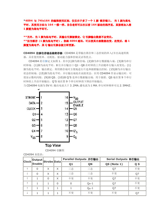
*4094 与74ls164 的编程使用区别,仅仅在于多了一个1脚锁存端口。
当1脚为高电平时,其使用方法与164一模一样。
各位老师可以在以前164驱动的程序里,直接将加入将1脚置为高电平即可。
**另外,当1脚为低电平时,其输出引脚被锁定,Q引脚输出数据不会变化。
**但当锁存(1脚为低电平时),你跟4094通讯,可以使其内部数据改变,改变后,将1脚置为高电平,其Q输出引脚会被立即更新。
CD4094 位移位存储总线寄存器: CD4094是带输出锁存和三态控制的串入/并出高速转换器,具有使用简单、功耗低、驱动能力强和控制灵活等优点。
CD4094的引脚定义如图1。
其中(1)脚为锁存端,(2)脚为串行数据输入端,(3)脚为串行时钟端。
(1)脚为高电平时,8位并行输出口Q1~Q8在时钟的上升沿随串行输入而变化;(1)脚为低电平时,输出锁定。
利用锁存端可方便地进行片选和级联输出控制。
(15)脚为并行输出状态控制端,(15)脚为低电平时,并行输出端处在高阻状态,在用CD4094作显示输出时,可使显示数码闪烁。
(9)脚QS、(10)脚Q′S是串行数据输出端,用于级联。
QS端在第9个串行时钟的上升沿开始输出,Q′S端在第9个串行时钟的下降沿开始输出.当CD4094电源为5V时,输出电流大于3.2MA,灌电流为1 MA。
串行时钟频率可达2.5MHZ。
CD4094引脚图CD4094真值表:Clock OutputEnableStrobe DataParallel Outputs 并行输出Serial Outputs 串行输出Q1 QN QS (Note 1) Q S↑0 X X 三态三态Q7 不变↓0 X X 三态三态不变Q7 ↑ 1 0 X 不变不变Q7 不变↑ 1 1 0 0 Q N-1 Q7 不变↑ 1 1 1 1 Q N-1 Q7 不变↓ 1 1 1 不变不变不变Q7CD4094内部电路方框图Absolute Maximum Ratings 绝对最大额定值:Supply Voltage电源电压(VDD) -0.5 to +18 VDCInput Voltage输入电压(VIN) 838电子-0.5 to VDD +0.5 VDCStorage Temperature Range储存温度范围(TS) -65℃to +150℃Power Dissipation功耗(PD)Dual-In-Line 普通双列封装新艺图库700 mWSmall Outline 小外形封装500 mWLead Temperature 焊接温度(TL)Soldering, 10 seconds)(焊接10秒)260℃Recommended Operating Conditions 建议操作条件:DC Supply Voltage 直流供电电压(VDD) +3.0 to +15 VDC Input Voltage输入电压(VIN) 838电子0 to VDD VDC Operating Temperature Range工作温度范围(TA) -40℃to +85℃DC Electrical Characteristics 直流电气特性:Symbol 符号Parameter参数Conditions 条件-40°C +25°C +85°C Units单位最小最大最小典型最大最小最大IDD QuiescentDeviceCurrent静态电流VDD = 5.0V 20 20 150μA VDD = 10V 40 40 300VDD = 15V 80 80 600VOL LOW LevelOutputVDD=5.0V|IO|≤1.μA0.05 0 0.05 0.05V VDD=10V 0.05 0 0.05 0.05Voltage 输出低电平电压VDD=15V0.050.050.05VOHHIGH Level OutputVoltage 输出高电平电压VDD=5.0V|IO|≤1μA 4.954.955.0 4.95 VVDD=10V 9.959.95 10.0 9.95VDD=15V14.9514.95 15.014.95VILLOW Level InputVoltage 输入低电平电压VDD = 5.0V, VO =0.5V or 4.5V 1.5 1.5 1.5 V VDD = 10V, VO =1.0V or 9.0V3.0 3.0 3.0 VDD = 15V, VO = 1.5V or 13.5V 838电子4.04.0 4.0VIHHIGH Level InputVoltage 输入高电平电压VDD = 5.0V, VO = 0.5V or 4.5V 3.5 3.5 3.5 VVDD = 10V, VO = 1.0V or 9.0V7.0 7.07.0 VDD = 15V, VO = 1.5V or 13.5V11.011.011.0 IOLLOW Level OutputCurrent 输出低电平电流 (Note 4)VDD=5.0V,VO=0.4V 0.52 0.44 0.88 0.36 mAVDD=10V,VO=0.5V 1.31.12.25 0.9VDD=15V,VO=1.5V 3.6 3.08.82.4 IOHHIGH Level OutputCurrent 输出高电平电流 (Note 4)VDD=5.0V,VO =4.6V -0.52 -0.44 0.88 -0.36 mAVDD =10V,VO= 9.5V -1.3-1.1 2.25-0.9VDD=15V,VO =13.5V -3.6 -3.0 8.8-2.4IINInputCurrent 输入电流 VDD =15V,VIN =0V -0.3 -0.3 -1.0 μA VDD=15V,VIN =15V0.30.31.0IOZ3-STATE OutputLeakage Current 3态输出漏电流VDD=15V,VIN=0V or 15V1110μAAC Electrical Characteristics 交流电气特性: Symbol符号Parameter 参数 838电子Conditions条件最小 典型 最大Units 单位tPHL, tPLH Propagation Delay Clock to QSVDD = 5.0V 300 600nsVDD = 10V 125 250VDD = 15V 95 190tPHL, tPLH Propagation Delay Clock to Q¢ SVDD =5.0V230 460nsVDD = 10V110 220VDD = 15V 75 150 nstPHL, tPLH Propagation Delay Clock to Parallel OutVDD = 5.0V 420 840nsVDD = 10V 195 390VDD = 15V 135 270tPHL, tPLH Propagation Delay Strobe to Parallel OutVDD = 5.0V 290 580nsVDD = 10V 145 290VDD = 15V 100 200tPHZ Propagation Delay HIGH Level to HIGHImpedanceVDD = 5.0V 140 280nsVDD = 10V 75 150VDD = 15V 55 110tPLZ Propagation Delay LOW Level to HIGHImpedanceVDD = 5.0V 140 280nsVDD = 10V 75 150VDD = 15V 55 110tPZH Propagation Delay HIGH Impedance to HIGHLevelVDD = 5.0V 140 280nsVDD = 10V 75 150VDD = 15V 55 110tPZL Propagation Delay HIGH Impedance to LOWLevelVDD = 5.0V 140 280nsVDD = 10V 75 150VDD = 15V 55 110tTHL, tTLH Transition Time过渡时间VDD = 5.0V 100 200nsVDD = 10V 50 100VDD = 15V 40 80tSU Set-Up Time Data to Clock 建立时间数据时钟VDD = 5.0V 80 40ns VDD = 10V 40 20VDD = 15V 20 10tr, tf Maximum Clock Rise and Fall Time最大时钟上升和下降时间VDD = 5.0V 1msVDD = 10V 1VDD = 15V 1tPC Minimum Clock Pulse Width最小时钟脉冲宽度VDD = 5.0V 200 100ns VDD = 10V 100 50VDD = 15V 83 40tPSMinimum Strobe Pulse WidthVDD = 5.0V 200 100nsVDD = 10V 80 40 VDD = 15V 70 35fmaxMaximum Clock Frequency 最大时钟频率VDD = 5.0V 1.5 3.0MHzVDD = 10V 3.0 6.0 VDD = 15V 4.0 8.0CINInput Capacitance 输入电容 Any Input 5.0 7.5 pF测试电路和3态时序图。
JIS D4207-1994 日标轮胎气门嘴标准中文版

日本工业标准汽车轮胎气门嘴D4207-1994 1.概述这一日本工业标准对于汽车(包括摩托车)上的轮胎气门嘴进行了标准规范。
(以下简称为气门嘴)备注:1 这份标准适用于装在工业汽车、工程车辆以及农业用车上的气门嘴。
2本文件主要参考以下标准:JIS D 4211 Tyre valve cores for automobilesJIS K 6259 Testing methods of resistance to ozone cracking for vulcanized rubberJIS Z 8703 Standard atmospheric conditions for testing3本标准中{}中的单位和数值是根据传统单位系统来的,是目前有效的标准。
然而1995.4.1后这些值才能做为有用的参考值。
2.定义为了实行这份标准,对以下进行定义:(1)气门嘴零件(a)气门嘴杆:柱状,连接在轮胎上,并具有一个充气放气(1)的孔道。
(见图1)气门嘴包括气门芯、密封帽、螺母、垫片、胶垫、气门芯外壳和底座。
解释(1):在某些情况下利用液体如水。
(b)气门芯:装在气门嘴杆内,作用是控制压缩空气。
(见图1)(c)胶垫:由橡胶制成,目的是保证嘴杆和轮辋或者气门芯外壳之间的气密性。
(见图2)(d)气门芯外壳:有一充气放气的孔,便于气门芯安装。
这零件是和气门嘴相连接。
(见图2)(e)气门嘴座:用来支撑气门嘴杆。
(见图1)(f)气门嘴延伸杆:目的是为了更容易地给双轮胎汽车的轮胎充气。
(2)气门嘴分类:(a)橡胶气门嘴(底部):有内胎气门嘴,在气门嘴杆底部有橡胶垫片。
(见附录图1)(b)橡胶气门嘴(全覆盖):有内胎气门嘴,气门嘴杆除了装密封帽的地方外,其它地方都用橡胶包裹住。
(见附录图2)(c)拧接气门嘴:有内胎气门嘴,底座由橡胶包裹住(见附录图3)(d)卡扣气门嘴:无内胎气门嘴(见附录图4),把气门嘴插入轮辋气门嘴孔中,通过紧压橡胶部分来保证气门嘴和轮辋间的气密性。
2948资料

A l l t h e b e n e f i t s o f t h e2945A b u t w i t h af oLow phase noise signal generatorHigh stability reference oscillator(OCXO)Accurate power measurement to 150 W Transient and harmonic analysisFast response high resolution bar charts peaking and nullingTracking generator with full offset track-Full span spectrum analyzer with ‘live’and listen Field OperationAt under 12kg the 2948 lightens the load to remote sites. The shape of the 2948 is ideal for carrying; the side handle ensures that the instrument is clear of the stairs when ascending buildings and the 2948’s depth is suitable for the instrument to be operated comfort-ably when it is placed on the floor.An optional bail arm handle is also available. This option allows a stowage cover to be fitted over the front panel for storage of adapters and further protection to the instrument’s front panel. Full opera-tion is possible from the protective ‘ever-ready’ case so that your investment is protected from transit damage.Stored settings may be recalled from internal memory or from a The spectrum analyzer provides spans from 100Hz per division to MHz per division and also has a fully adjustable reference level. Speed is comparable with analog analyzers, allowing real time adjust-SimulationThe 2948 simulates the signalling protocol that the radio would seeCard -with real time clockThe memory card drive meets the PCMCIA standard format for PC cards. The 2948 provides a DOS based filing system that allows trans-AnalysisThe ability to capture transients on the rising or falling edge of aOUTPUT LEVELOutput Level RangeN I C A N D T R A N S I E N T A N A L Y S I S。
lm2904中文资料
LM2904包含两个具有高增益和内部频率补偿的独立双路运算放大器,适用于具有宽电源电压范围和双电源工作模式的单电源。
在推荐的工作条件下,电源电流与电源电压无关。
它的应用范围包括读出放大器,DC增益模块以及所有其他可由单个电源提供运算放大器的场合。
该警报器可以检测到人体发出的红外线。
当人们进入警报监视区域时,他们会发出警报声。
适用于家庭,办公室,仓库和实验室等重要场合的防盗报警器。
工作原则它由红外传感器,信号放大电路,电压比较器,延迟电路和音频报警电路组成。
当红外检测传感器IC1检测到从人体前方发出的红外信号时,微弱的电信号由IC1的引脚②输出,由晶体管VT1构成的第一级放大电路放大,然后输入到运算放大器IC2通过C2实现高增益和低噪声放大。
此时,IC2的引脚①输出的信号足够强。
IC3用作电压比较器,其第五引脚由R10和VD1提供参考电压。
当从IC2①的引脚①输出的信号电压到达IC3的引脚⑥时,比较两个输入端子的电压,然后IC3的引脚from从原始的高电平变为低电平。
IC4是警报延迟电路,R14和C6构成延迟电路,持续约1分钟。
当IC3的引脚low 变为低电平时,C6通过VD2放电,而IC4的引脚②变为低电平,与IC4的引脚③的参考电压进行比较。
当其低于参考电压时,IC4的引脚①变为高电平,VT2开启,并且蜂鸣器BL开启并发出警报声。
人体的红外信号消失后,IC3的引脚resume恢复高电平输出,此时VD2关闭。
由于C6两端的电压不能突然变化,因此请通过R14缓慢地给C6充电。
当C6两端的电压高于参考电压时,IC4的①引脚变为低电平,时间约为1分钟,即警报持续1分钟。
由VT3,R20和C8组成的启动延迟电路大约需要一分钟,其设置主要是为了防止用户在启动后立即发出警报,以便用户有足够的时间离开监视站点,同时,可以防止在停电后再次拨打电话时出现误报。
该器件由9-12 V直流电源供电,具有T降压,全桥U整流和C10滤波。
光电复合缆

输入过欠压保护 输出过压保护
输出过流保护
对地悬浮 短路保护 开路保护
直流远供系统安全性能保护(二)
点对多点的应用情况时,其中一设备有故障时不会影响到另一设备的正常运行 上述保护动作的同时,不同颜色指示灯亮,指示相应故障类型 远供电源局端、远端设备工作温度超过额定值时,远供电源局端机会自动停止输 出,保护设备。同时输出告警信号 上述保护动作的同时,干节点闭合, 故障信息上传给监控设备 用户如不及时修理,故障未经排除,则无法合闸通电 线路发生瞬间冲击而可能有危险时,重合闸漏电开关立即断开 冲击过后,如果线路安全,重合闸漏电开关会自动重新合闸通电 连续重合闸3次失败后,重合闸漏电开关将断开并报警。
入网用光电混合缆》
23
23
烽火光电混合缆典型结构(一)
GDS-(4~24)+2*(1.5mm2~10mm2)
电源线 阻水纱 中芯加强件 纤膏 阻水带 UV 光纤 钢带铠装 PE 护套 适用于架空铺设(最常用型号) 类同与GYTS普通室外光缆采用钢带铠装 采用半干式结构
24 24
烽火光电混合缆典型结构(二)
12
-48Vdc/220Vac
12
远供方案4-远端集中供电解决方案2
远端通信设备 远供局端电源 -48VDC 380VDC
复合光缆或电缆
48VD C /220V ac
远供远端电源 配 置: 局端电源:48VDC/380VDC:N+1并联冗余; 远端电源:户外机柜方式,功率分配单元和远端模块( 380VDC/48VDC或380VDC/220VAC)置于户外机柜内,其中 交流远端每只模块对立对单一负载供电,直流远端采用并联冗余 系统经直流配电给负载供电。 功率范围:局端: ≥ 1500W;远端:400W~800W/只 特 点:局端电源模块采用N+1并联冗余模式,输出通过功率分 配模块对各通信设备进行单独功率配置,提高了通用配置对不同 容量负载设备的兼容性。 适用范围:适用于远端设备集中在一点,但离局端远的场合。 13 13
1956344资料
Extract from the onlinecatalogCC 2,5/10-GFL-5,08P26THROrder No.: 1956344The illustration shows a left and a right plug, as 8-pos. versionhttp://eshop.phoenixcontact.de/phoenix/treeViewClick.do?UID=1956344Modular headers, left, with screw flange, pin length: 2.6 mm, 5.08 mm pitch, 10-pos.http://Please note that the data givenhere has been taken from theonline catalog. For comprehensiveinformation and data, please referto the user documentation. TheGeneral Terms and Conditions ofUse apply to Internet downloads. Technical dataDimensions / positionsPitch 5.08 mmDimension a45.72 mmNumber of positions10Pin dimensions 1 x 1 mmPin spacing 5.08 mmHole diameter 1.4 mmTechnical dataInsulating material group IIIaRated surge voltage (III/3) 4 kVRated surge voltage (III/2) 4 kVRated surge voltage (II/2) 4 kVRated voltage (III/2)320 VRated voltage (II/2)400 VConnection in acc. with standard EN-VDENominal current I N12 ANominal voltage U N250 VMaximum load current12 A (per position)Insulating material LCPInflammability class acc. to UL 94V0Certificates / ApprovalsApproval logoCULNominal voltage U N300 VNominal current I N10 AULNominal voltage U N300 VNominal current I N10 ACertification CUL, ULAccessoriesItem Designation DescriptionGeneral1954362CR-MSTB NAT HT HT coding section, is pushed into the recess on the header beforethe reflow process, made of highly temperature-resistant, beigeinsulating materialMarking1051993B-STIFT Marker pen, for manual labeling of unprinted Zack strips, smear-proof and waterproof, line thickness 0.5 mm0804303SK 5,08/3,8: 0-9Marker card, printed horizontally, self-adhesive, 10-section markerstrip, 12 identical decades marked 0-9, sufficient for 120 terminalblocks0804293SK 5,08/3,8:FORTL.ZAHLEN Marker card, printed horizontally, self-adhesive, 12 identicaldecades marked 1-10, 11-20 etc. up to 91-(99)100, sufficient for120 terminal blocks0805085SK 5,08/3,8:SO Marker card, special printing, self-adhesive, labeled acc. tocustomer requirements, 12 identical marker strips per card, max.25-position labeling per strip, color: white0805412SK 5,08/3,8:UNBEDRUCKT Marker cards, unprinted, with pitch divisions, self-adhesive, 10-section marker strips, 12 strips per card, can be labeled with theM-PENPlug/Adapter1734401CR-MSTB Coding section, inserted into the recess in the header or theinverted plug, red insulating materialDrawingsApplication drawingDrilling diagramDimensioned drawingBottom view, free space for solder paste, 0.5mm deepAddressPHOENIX CONTACT GmbH & Co. KGFlachsmarktstr. 832825 Blomberg,GermanyPhone +49 5235 3 00Fax +49 5235 3 41200http://www.phoenixcontact.de© 2008 Phoenix ContactTechnical modifications reserved;。
lm2904中文资料汇总(lm2904引脚图及功能
lm2904中文资料汇总(lm2904引脚图及功能LM2904概述(DescripTIon)LM2904内部包括有两个独立的、高增益、内部频率补偿的双运算放大器,适合于电源电压范围很宽的单电源使用,也适用于双电源工作模式,在推荐的工作条件下,电源电流与电源电压无关。
它的使用范围包括传感放大器、直流增益模块和其他所有可用单电源供电的使用运算放大器的场合。
LM2904的封装形式有塑封8引线双列直插式和贴片式。
LM2904特性(Features)内部频率补偿直流电压增益高(约100dB)单位增益频带宽(约1MHz)电源电压范围宽:单电源(3—30V);双电源(±1.5一±15V)低功耗电流,适合于电池供电低输入偏流低输入失调电压和失调电流共模输入电压范围宽,包括接地差模输入电压范围宽,等于电源电压范围输出电压摆幅大(0至Vcc-1.5V)lm2904应用电路(一)该报警器能探测人体发出的红外线,当人进入报警器的监视区域内,即可发出报警声,适用于家庭、办公室、仓库、实验室等比较重要场合防盗报警。
工作原理该装置电路原理见图1。
由红外线传感器、信号放大电路、电压比较器、延时电路和音响报警电路等组成。
红外线探测传感器IC1探测到前方人体辐射出的红外线信号时,由IC1的②脚输出微弱的电信号,经三极管VT1等组成第一级放大电路放大,再通过C2输入到运算放大器IC2中进行高增益、低噪声放大,此时由IC2①脚输出的信号已足够强。
IC3作电压比较器,它的第⑤脚由R10、VD1提供基准电压,当IC2①脚输出的信号电压到达IC3的⑥脚时,两个输入端的电压进行比较,此时IC3的⑦脚由原来的高电平变为低电平。
IC4为报警延时电路,R14和C6组成延时电路,其时间约为1分钟。
当IC3的⑦脚变为低电平时,C6通过VD2放电,此时IC4的②脚变为低电平,它与IC4的③脚基准电压进行比较,当它低于其基准电压时,IC4的①脚变为高电平,VT2导通,讯响器BL通电发出报警声。
- 1、下载文档前请自行甄别文档内容的完整性,平台不提供额外的编辑、内容补充、找答案等附加服务。
- 2、"仅部分预览"的文档,不可在线预览部分如存在完整性等问题,可反馈申请退款(可完整预览的文档不适用该条件!)。
- 3、如文档侵犯您的权益,请联系客服反馈,我们会尽快为您处理(人工客服工作时间:9:00-18:30)。
Capable of driving loads to 4 A at supply voltages to 60 V (induc-tive loads to 35 V), the UDN2944W is a quad high-current, high-voltage source driver. Each of the four power drivers can provide space- and cost-saving interface between low-level signal-processing circuits and high-power loads in harsh environments.Individual supply lines have been provided for each pair of drivers so that different supplies can be used to drive multiple loads. The controlling inputs are TTL or CMOS compatible. The outputs include transient-suppression diodes for inductive loads.This quad Darlington array is designed to serve as an interface between low-level circuitry and peripheral-power loads such as sole-noids, motors, incandescent displays, heaters, and similar loads of up to 240 W per channel. The UDN2944W is an ideal complement to the UDN2878W quad 4 A sink driver.For maximum power-handling capability, the UDN2944W driver is supplied in a 12-pin single in-line, power-tab package that allows efficient attachment of an external heat sink for maximum allowable package power dissipation. An external heat sink is usually required for proper operation of this device. The tab is at ground potential and needs no insulation.FEATURESI Output Current to 4 A I Output Voltage to 60 V I Loads to 960 WI Integral Output Suppression Diodes I TTL and CMOS Compatible Inputs I Plastic Single In-Line Package IHeat-Sink Tab2944QUAD HIGH-CURRENT,HIGH-VOLTAGE SOURCE DRIVERABSOLUTE MAXIMUM RATINGS at +25°C Free-Air TemperatureSupply Voltage Range, V S ..... 10 V to 60 V Output Current, I OUT(continuous)............................... -4.0 A (peak)......................................... -5.0 A Input Voltage, V IN ................................ 15 V Package Power Dissipation,P D ....................................... See Graph Operating Temperature Range,T A ................................ -20°C to +85°C Storage Temperature Range,T S .............................. -55°C to +150°C Output current rating will be limited by ambient temperature, duty cycle, heat sinking, air flow, and number of outputsconducting. Under any set of conditions, do not exceed the -5.0 A peak current or a junction temperature of +150°C.V SData Sheet 29309.10†2944QUAD HIGH-CURRENT,HIGH-VOLTAGESOURCE DRIVER115 Northeast Cutoff, Box 15036Worcester, Massachusetts 01615-0036 (508) 853-5000PARTIAL SCHEMATIC5075100125150106420A L L O W A B L E P A C K A G E P O W E R D I S S I P A T I O N I N W A T T STEMPERATURE IN °C825Dwg. GP-012BW Copyright © 1986, 2000 Allegro MicroSystems, Inc.TRUTH TABLEINPUT ENABLEOUTPUTLL L H L H L H L HHLNOTE:Pin 3 must be connected to V S foroperation of input logic gates.Dwg. No. A-13,0582944QUAD HIGH-CURRENT,HIGH-VOLTAGE SOURCE DRIVERELECTRICAL CHARACTERISTICS at T A = +25°C, T J ≤ +150°C, V S = 60 V, V ENABLE = 0 V (unless otherwise noted).Limits Characteristic Symbol Test ConditionsMin.Max.Units Supply Voltage Range V S 1060V Output Leakage Current I CEX V OUT = 0 V, V ENABLE = 2.4 V —50µA Output Sustaining Voltage V CE(sus)I OUT = -4 A, L = 3 mH 35—V Output Saturation VoltageV CE(SAT)I OUT = -1 A, V IN = 2.4 V — 1.8V I OUT = -4 A, V IN = 2.4 V— 2.5V Input VoltageLogic 1V IN(1) or V ENABLE(1) 2.0—V Logic 0V IN(0) or V ENABLE(0)—0.8V Input CurrentLogic 1V IN(1) or V ENABLE(1) = 2.4 V —220µA V IN(1) or V ENABLE(1) = 12 V— 1.5mA Logic 0V IN(0) or V ENABLE(0) = 0.8 V —50µA Total Supply CurrentI S All drivers on, All outputs open —25mA Clamp Diode Leakage Current I R V R = 60 V —50µA Clamp Diode Forward Voltage V F I F = 4 A— 2.2V Turn-On Delay t ON 0.5 E in to 0.5 E out , R L = 15 Ω— 2.0µs Turn-Off Delayt OFF0.5 E in to 0.5 E out , R L = 15 Ω—10µsNOTE: Negative current is defined as coming out of (sourcing) the device being tested.2944QUAD HIGH-CURRENT,HIGH-VOLTAGESOURCE DRIVER115 Northeast Cutoff, Box 15036Worcester, Massachusetts 01615-0036 (508) 853-5000Dimensions in Inches(controlling dimensions)NOTES:1.Lead thickness is measured at seating plane or below.2.Lead spacing tolerance is non-cumulative.3.Exact body and lead configuration at vendor’s option within limits shown.4.Lead gauge plane is 0.030” below seating plane.5.Supplied in standard sticks/tubes of 15 devices.Dwg. MP-007 in2944 QUAD HIGH-CURRENT,HIGH-VOLTAGESOURCE DRIVER Dimensions in Millimeters (for reference only)NOTES:1.Lead thickness is measured at seating plane or below.2.Lead spacing tolerance is non-cumulative.3.Exact body and lead configuration at vendor’s option within limits shown.4.Lead gauge plane is 0.762 mm below seating plane.5.Supplied in standard sticks/tubes of 15 devices.Dwg. MP-007 mm2944QUAD HIGH-CURRENT,HIGH-VOLTAGESOURCE DRIVER115 Northeast Cutoff, Box 15036Worcester, Massachusetts 01615-0036 (508) 853-5000This page intentionally left blank2944 QUAD HIGH-CURRENT,HIGH-VOLTAGESOURCE DRIVERThe products described here are manufactured under one or more U.S. patents or U.S. patents pending.Allegro MicroSystems, Inc. reserves the right to make, from time to time, such departures from the detail specifications as may be required to permit improvements in the performance, reliability, or manufacturability of its products. Before placing an order, the user is cautioned to verify that the information being relied upon is current.Allegro products are not authorized for use as critical components in life-support devices or systems without express written approval.The information included herein is believed to be accurate and reliable. However, Allegro MicroSystems, Inc. assumes no responsi-bility for its use; nor for any infringement of patents or other rights of third parties which may result from its use.2944QUAD HIGH-CURRENT,HIGH-VOLTAGESOURCE DRIVER115 Northeast Cutoff, Box 15036Worcester, Massachusetts 01615-0036 (508) 853-5000POWER SOURCE DRIVERSIN ORDER OF 1) OUTPUT CURRENT, 2) OUTPUT VOLTAGE, 3) NUMBER OF DRIVERSOutput Ratings *FeaturesSerial Latched Diode Saturated InternalmA V #Input Drivers Clamp Outputs Protection Part Number†-2560 8–X –––58156010XX active pull-down ––5810-F and 6809/106012X X active pull-down ––5811 and 68116020X X active pull-down ––5812-F and 68126032X X active pull-down ––5818-F and 681885 8–––––6118-120-25 8––X X –258530 8––X X –298550 8X X X X –5895-35035 8––X –X 298750 8––X ––2981 and 298250 8X X X ––5891-50 8––X ––258080 8––X ––2983 and 298480 8X X X ––5890-80 8––X ––2588-50061–––MOSFET X 2525 and 253562–––MOSFET X 2526 and 2536-4000604––X ––2944over-current protection voltage limits.†Complete part number includes additional characters to indicate operating temperature range and package style.。