ChipSee-EVM3359(RevA1)
RS3219 REV A.3 1 低功耗低落电压300mA低噪声低IQ线性调压电源模块说明书
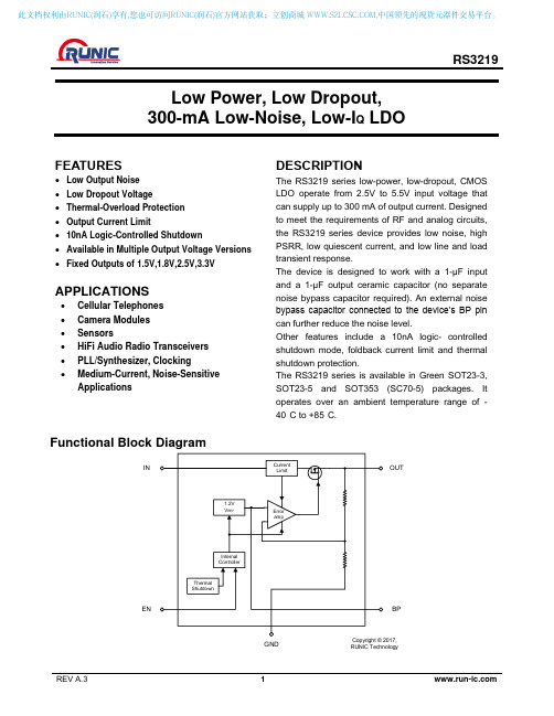
RS3219 Low Power, Low Dropout,300-mA Low-Noise, Low-I Q LDOFEATURESLow Output NoiseLow Dropout VoltageThermal-Overload ProtectionOutput Current Limit10nA Logic-Controlled ShutdownAvailable in Multiple Output Voltage Versions Fixed Outputs of 1.5V,1.8V,2.5V,3.3VAPPLICATIONS•Cellular Telephones•Camera Modules•Sensors•HiFi Audio Radio Transceivers•PLL/Synthesizer, Clocking•Medium-Current, Noise-SensitiveApplications DESCRIPTIONThe RS3219 series low-power, low-dropout, CMOS LDO operate from 2.5V to 5.5V input voltage that can supply up to 300 mA of output current. Designed to meet the requirements of RF and analog circuits, the RS3219 series device provides low noise, high PSRR, low quiescent current, and low line and load transient response.The device is designed to work with a 1-µF input and a 1-µF output ceramic capacitor (no separate noise bypass capacitor required). An external noise bypass capacitor connected to the device’s BP pin can further reduce the noise level.Other features include a 10nA logic- controlled shutdown mode, foldback current limit and thermal shutdown protection.The RS3219 series is available in Green SOT23-3, SOT23-5 and SOT353 (SC70-5) packages. It operates over an ambient temperature range of -40°C to +85°C.Functional Block DiagramINEN BPOUTGND RUNIC TechnologyPin Configuration and Functions (Top View)IN ENOUTGND BPSOT23-5/SOT353(SC70-5)GND OUTINSOT23-3Absolute Maximum Ratings(1)(2)ratings only, and functional operation of the device at these or any other conditions beyond those indicated under Recommended Operating Conditions is not implied. Exposure to absolute-maximum-rated conditions for extended periods may affect device reliability.(2) All voltages are with respect to the GND pin.(3) Internal thermal shutdown circuitry protects the device from permanent damage.Recommended Operating Conditions(1)ELECTRICAL CHARACTERISTICS(V IN = V OUT (NOMINAL) + 0.5V (1), Full = -40 to +85, unless otherwise noted.)PARAMETER SYMBOL CONDITIONS TEMP MIN TYP MAX UNITS Input Voltage V IN+25 2.5(1) 5.5V Output Voltage Accuracy (1)I OUT = 0.1mA +25-3.0 6.0% Maximum Output Current (1)+25300mA Current Limit (1)I LIM+25300500mA Ground Pin Current I Q No load, EN = 2V +25100200µADropout Voltage (2)I OUT = 1mA+251.5mV I OUT = 300mA 280400Line Regulation (1)ΔV LNR V IN = 2.5V or (V OUT + 0.5V) to 5.5V,I OUT = 1mA+250.030.09%/VLoad Regulation ΔV LDR I OUT =0.1mA to 300mA, C OUT = 1µF, +250.0020.005%/mAOutput Voltage Noise e n f = 10Hz to 100kHz, C BP = 0.1µF,C OUT = 10µF+2528µV RMSPower Supply Rejection Ratio PSRR C BP = 0.1μF, I LOAD = 50mA,C OUT = 1μF, V IN = V OUT+1Vf = 217Hz+2567dBf = 1kHz +2564dBSHUTDOWN (3)EN Input Threshold V IHV IN = 2.5V to 5.5V, V EN = -0.3V to V INFull0.7xV IN V V IL Full 0.3EN Input Bias Current I B(SHDN)EN = 0V or EN = 5.5V +250.011μA Full 0.01Shutdown Supply Current I Q(SHDN)EN = 0.4V Full 0.01μA Shutdown Exit Delay (4)C BP = 0.01μF, C OUT = 1μF, No Load +2530μs THERMAL PROTECTIONThermal ShutdownTemperatureT SHDN150Thermal Shutdown Hysteresis ΔT SHDN15NOTES:1. V IN = V OUT (NOMINAL) + 0.5V or2.5V, whichever is greater.2. The dropout voltage is defined as V IN - V OUT, when V OUT is 100mV below the value of V OUT for V IN = V OUT + 0.5V.(Only applicable for V OUT = +2.5V to +5.0V.)3. V EN = -0.3V to V IN4. Time needed for V OUT to reach 90% of final value.TYPICAL APPLICATION CIRCUITBP OUTOUT 1uFC BP 5Pin Typical CircuitVINOUT C C OUT 1uF3Pin Typical CircuitV IN = V OUT (NOMINAL) + 0.5V, C IN= 1μF, C OUT= 1μF, C BP= 0.1μF, T A = +25℃, unless otherwise noted.START UP2V0V0V3VENV OUTTime(20us/div)SHUTDOWN2V0V0V3.3VENV OUTTime(200us/div)LOAD-TRANSIENT RESPONSE300mA0mA3.1V3.5VI LOADV OUTTime(100us/div)3.3VLOAD-TRANSIENT RESPONSE50mA0mA3.1V3.5VI LOADV OUTTime(100us/div)3.3VV IN = V OUT (NOMINAL) + 0.5V, C IN = 1μF, C OUT = 1μF, C BP = 0.1μF, T A = +25℃, unless otherwise noted.PACKAGE OUTLINE DIMENSIONSSOT23-3RECOMMENDED LAND PATTERN (Unit: mm)SOT23-5RECOMMENDED LAND PATTERN (Unit: mm)RS321911SOT353 (SC70-5)。
微斯米微波式芯片公司2014年产品说明书
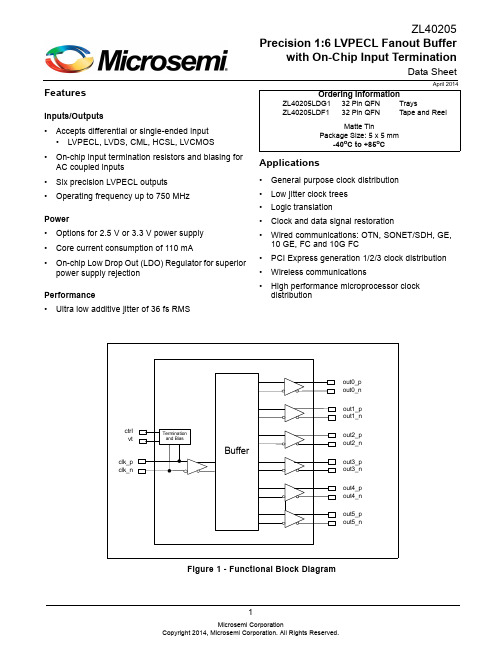
1FeaturesInputs/Outputs •Accepts differential or single-ended input •LVPECL, LVDS, CML, HCSL, LVCMOS •On-chip input termination resistors and biasing for AC coupled inputs•Six precision LVPECL outputs •Operating frequency up to 750 MHzPower •Options for 2.5 V or 3.3 V power supply •Core current consumption of 110 mA•On-chip Low Drop Out (LDO) Regulator for superior power supply rejectionPerformance •Ultra low additive jitter of 36 fs RMSApplications•General purpose clock distribution •Low jitter clock trees •Logic translation•Clock and data signal restoration•Wired communications: OTN, SONET/SDH, GE,10 GE, FC and 10G FC•PCI Express generation 1/2/3 clock distribution •Wireless communications•High performance microprocessor clock distributionApril 2014Figure 1 - Functional Block DiagramZL40205Precision 1:6 LVPECL Fanout Bufferwith On-Chip Input TerminationData SheetOrdering InformationZL40205LDG1 32 Pin QFN TraysZL40205LDF132 Pin QFNTape and ReelMatte TinPackage Size: 5 x 5 mm-40o C to +85o CTable of ContentsFeatures . . . . . . . . . . . . . . . . . . . . . . . . . . . . . . . . . . . . . . . . . . . . . . . . . . . . . . . . . . . . . . . . . . . . . . . . . . . . . . . . . 1 Inputs/Outputs . . . . . . . . . . . . . . . . . . . . . . . . . . . . . . . . . . . . . . . . . . . . . . . . . . . . . . . . . . . . . . . . . . . . . . . . .1 Power . . . . . . . . . . . . . . . . . . . . . . . . . . . . . . . . . . . . . . . . . . . . . . . . . . . . . . . . . . . . . . . . . . . . . . . . . . . . . . . .1 Performance . . . . . . . . . . . . . . . . . . . . . . . . . . . . . . . . . . . . . . . . . . . . . . . . . . . . . . . . . . . . . . . . . . . . . . . . . . .1 Applications . . . . . . . . . . . . . . . . . . . . . . . . . . . . . . . . . . . . . . . . . . . . . . . . . . . . . . . . . . . . . . . . . . . . . . . . . . . . . 1 Change Summary . . . . . . . . . . . . . . . . . . . . . . . . . . . . . . . . . . . . . . . . . . . . . . . . . . . . . . . . . . . . . . . . . . . . . . . . . 41.0 Package Description . . . . . . . . . . . . . . . . . . . . . . . . . . . . . . . . . . . . . . . . . . . . . . . . . . . . . . . . . . . . . . . . . . . .52.0 Pin Description. . . . . . . . . . . . . . . . . . . . . . . . . . . . . . . . . . . . . . . . . . . . . . . . . . . . . . . . . . . . . . . . . . . . . . . . .63.0 Functional Description . . . . . . . . . . . . . . . . . . . . . . . . . . . . . . . . . . . . . . . . . . . . . . . . . . . . . . . . . . . . . . . . . .73.1 Clock Inputs. . . . . . . . . . . . . . . . . . . . . . . . . . . . . . . . . . . . . . . . . . . . . . . . . . . . . . . . . . . . . . . . . . . . . . . . .73.2 Clock Outputs . . . . . . . . . . . . . . . . . . . . . . . . . . . . . . . . . . . . . . . . . . . . . . . . . . . . . . . . . . . . . . . . . . . . . .123.3 Device Additive Jitter. . . . . . . . . . . . . . . . . . . . . . . . . . . . . . . . . . . . . . . . . . . . . . . . . . . . . . . . . . . . . . . . .153.4 Power Supply . . . . . . . . . . . . . . . . . . . . . . . . . . . . . . . . . . . . . . . . . . . . . . . . . . . . . . . . . . . . . . . . . . . . . .163.4.1 Sensitivity to power supply noise. . . . . . . . . . . . . . . . . . . . . . . . . . . . . . . . . . . . . . . . . . . . . . . . . . .163.4.2 Power supply filtering. . . . . . . . . . . . . . . . . . . . . . . . . . . . . . . . . . . . . . . . . . . . . . . . . . . . . . . . . . . .163.4.3 PCB layout considerations. . . . . . . . . . . . . . . . . . . . . . . . . . . . . . . . . . . . . . . . . . . . . . . . . . . . . . . .164.0 AC and DC Electrical Characteristics . . . . . . . . . . . . . . . . . . . . . . . . . . . . . . . . . . . . . . . . . . . . . . . . . . . . .175.0 Performance Characterization . . . . . . . . . . . . . . . . . . . . . . . . . . . . . . . . . . . . . . . . . . . . . . . . . . . . . . . . . . .206.0 Typical Behavior . . . . . . . . . . . . . . . . . . . . . . . . . . . . . . . . . . . . . . . . . . . . . . . . . . . . . . . . . . . . . . . . . . . . . .217.0 Package Characteristics . . . . . . . . . . . . . . . . . . . . . . . . . . . . . . . . . . . . . . . . . . . . . . . . . . . . . . . . . . . . . . .238.0 Mechanical Drawing . . . . . . . . . . . . . . . . . . . . . . . . . . . . . . . . . . . . . . . . . . . . . . . . . . . . . . . . . . . . . . . . . . .24List of FiguresFigure 1 - Functional Block Diagram . . . . . . . . . . . . . . . . . . . . . . . . . . . . . . . . . . . . . . . . . . . . . . . . . . . . . . . . . . . . 1 Figure 2 - Pin Connections . . . . . . . . . . . . . . . . . . . . . . . . . . . . . . . . . . . . . . . . . . . . . . . . . . . . . . . . . . . . . . . . . . . 5 Figure 3 - Simplified Diagram of Input Stage. . . . . . . . . . . . . . . . . . . . . . . . . . . . . . . . . . . . . . . . . . . . . . . . . . . . . . 7 Figure 4 - Clock Input - LVPECL - DC Coupled. . . . . . . . . . . . . . . . . . . . . . . . . . . . . . . . . . . . . . . . . . . . . . . . . . . . 8 Figure 5 - Clock Input - LVPECL - AC Coupled. . . . . . . . . . . . . . . . . . . . . . . . . . . . . . . . . . . . . . . . . . . . . . . . . . . . 8 Figure 6 - Clock Input - LVDS - DC Coupled . . . . . . . . . . . . . . . . . . . . . . . . . . . . . . . . . . . . . . . . . . . . . . . . . . . . . . 9 Figure 7 - Clock Input - LVDS - AC Coupled . . . . . . . . . . . . . . . . . . . . . . . . . . . . . . . . . . . . . . . . . . . . . . . . . . . . . . 9 Figure 8 - Clock Input - CML- AC Coupled . . . . . . . . . . . . . . . . . . . . . . . . . . . . . . . . . . . . . . . . . . . . . . . . . . . . . . 10 Figure 9 - Clock Input - HCSL- AC Coupled . . . . . . . . . . . . . . . . . . . . . . . . . . . . . . . . . . . . . . . . . . . . . . . . . . . . . 10 Figure 10 - Clock Input - AC-coupled Single-Ended . . . . . . . . . . . . . . . . . . . . . . . . . . . . . . . . . . . . . . . . . . . . . . . 11 Figure 11 - Clock Input - DC-coupled 3.3V CMOS. . . . . . . . . . . . . . . . . . . . . . . . . . . . . . . . . . . . . . . . . . . . . . . . . 11 Figure 12 - Simplified Output Driver. . . . . . . . . . . . . . . . . . . . . . . . . . . . . . . . . . . . . . . . . . . . . . . . . . . . . . . . . . . . 12 Figure 13 - LVPECL Basic Output Termination . . . . . . . . . . . . . . . . . . . . . . . . . . . . . . . . . . . . . . . . . . . . . . . . . . . 12 Figure 14 - LVPECL Parallel Output Termination. . . . . . . . . . . . . . . . . . . . . . . . . . . . . . . . . . . . . . . . . . . . . . . . . . 13 Figure 15 - LVPECL Parallel Thevenin-Equivalent Output Termination. . . . . . . . . . . . . . . . . . . . . . . . . . . . . . . . . 13 Figure 16 - LVPECL AC Output Termination . . . . . . . . . . . . . . . . . . . . . . . . . . . . . . . . . . . . . . . . . . . . . . . . . . . . . 14 Figure 17 - LVPECL AC Output Termination for CML Inputs. . . . . . . . . . . . . . . . . . . . . . . . . . . . . . . . . . . . . . . . . 14 Figure 18 - Additive Jitter. . . . . . . . . . . . . . . . . . . . . . . . . . . . . . . . . . . . . . . . . . . . . . . . . . . . . . . . . . . . . . . . . . . . 15 Figure 19 - Decoupling Connections for Power Pins. . . . . . . . . . . . . . . . . . . . . . . . . . . . . . . . . . . . . . . . . . . . . . . 16 Figure 20 - Differential and Single-Ended Output Voltages Parameter Definitions . . . . . . . . . . . . . . . . . . . . . . . . 18 Figure 21 - Input To Output Timing . . . . . . . . . . . . . . . . . . . . . . . . . . . . . . . . . . . . . . . . . . . . . . . . . . . . . . . . . . . . 19Change SummaryPage Item Change1Applications Added PCI Express clock distribution.6Pin Description Added exposed pad to Pin Description.8Figure 4 and Figure 5Removed 22 ohm series resistors from Figure 4 and 5. These resistor are not required; however there is no impact to performance if the resistors are included.16Power supply filtering 18Figure 20Clarification of V ID and V OD .Below are the changes from the February 2013 issue to the April 2014 issue:Page Item Change8Figure 4Changed text to indicate the circuit is not recommended for VDD_driver=2.5V.Below are the changes from the November 2012 issue to the February 2013 issue:Corrected typo of 0.3 Ohm to 0.15 Ohm.1.0 Package DescriptionThe device is packaged in a 32 pin QFNFigure 2 - Pin Connections2.0 Pin DescriptionPin # Name Description3, 6clk_p, clk_n,Differential Input (Analog Input). Differential (or single ended) input signals.For all input configurations see “Clock Inputs” on page 728, 27, 26, 25, 24, 23, 18, 17, 16, 15, 14, 13out0_p, out0_nout1_p, out1_nout2_p, out2_nout3_p, out3_nout4_p, out4_nout5_p, out5_nDifferential Output (Analog Output). Differential outputs.9, 19,22, 32vdd Positive Supply Voltage. 2.5 V DC or 3.3 V DC nominal.1, 8vdd_core Positive Supply Voltage. 2.5 V DC or 3.3 V DC nominal.2, 7,20, 21gnd Ground. 0 V.4vt On-Chip Input Termination Node (Analog). Center tap between internal 50 Ohmtermination resistors.The use of this pin is detailed in section 3.1, “Clock Inputs“, for various input signal types.5ctrl Digital Control for On-Chip Input Termination (Input). Selects differential input mode;0: DC coupled LVPECL or LVDS modes1: AC coupled differential modesThis pin are internally pulled down to GND. The use of this pin is detailed in section 3.1,“Clock Inputs“, for various input signal types.10, 11,12, 29,30, 31NC No Connection. Leave unconnected.Exposed Pad Device GND.3.0 Functional DescriptionThe ZL40205 is an LVPECL clock fan out buffer with six output clock drivers capable of operating at frequencies up to 750MHz.The ZL40205 provides an internal input termination network for DC and AC coupled inputs; optional input biasing for AC coupled inputs is also provided. The ZL40205 can accept DC or AC coupled LVPECL and LVDS input signals, AC coupled CML or HCSL input signals, and single ended signals. A pin compatible device with external termination is also available.The ZL40205 is designed to fan out low-jitter reference clocks for wired or optical communications applications while adding minimal jitter to the clock signal. An internal linear power supply regulator and bulk capacitors minimize additive jitter due to power supply noise. The device operates from 2.5V+/-5% or 3.3V+/-5% supply. Its operation is guaranteed over the industrial temperature range -40°C to +85°C.The device block diagram is shown in Figure 1; its operation is described in the following sections.3.1 Clock InputsThe device has a differential input equipped with two on-chip 50 Ohm termination resistors arranged in series with a center tap. The input can accept many differential and single-ended signals with AC or DC coupling as appropriate. A control pin is available to enable internal biasing for AC coupled inputs. A block diagram of the input stage is in Figure 3.Receiverclk_n 50clk_pVt 50BiasctrlFigure 3 - Simplified Diagram of Input StageThis following figures give the components values and configuration for the various circuits compatible with the input stage and the use of the Vt and ctrl pins in each case.In the following diagrams where the ctrl pin is logically one and the Vt pin is not connected, the Vt pin can be instead connected to VDD with a capacitor. A capacitor can also help in Figure 4 between Vt and VDD. This capacitor will minimize the noise at the point between the two internal termination resistors and improve the overall performance of the device.Figure 4 - Clock Input - LVPECL - DC CoupledFigure 5 - Clock Input - LVPECL - AC CoupledFigure 6 - Clock Input - LVDS - DC CoupledFigure 7 - Clock Input - LVDS - AC CoupledFigure 8 - Clock Input - CML- AC CoupledFigure 9 - Clock Input - HCSL- AC CoupledFigure 10 - Clock Input - AC-coupled Single-EndedFigure 11 - Clock Input - DC-coupled 3.3V CMOS3.2 Clock OutputsLVPECL has a very low output impedance and a differential signal swing between 1V and 1.6 V. A simplified diagram for the output stage is shown in Figure 12.The LVPECL to LVDS output termination is not shown since there is a different device with the same inputs and LVDS outputs.out_pout_nFigure 12 - Simplified Output DriverThe methods to terminate the ZL40205 LVPECL drivers are shown in the following figures.Figure 15 - LVPECL Parallel Thevenin-Equivalent Output TerminationFigure 16 - LVPECL AC Output TerminationFigure 17 - LVPECL AC Output Termination for CML Inputs3.3 Device Additive JitterThe ZL40205 clock fanout buffer is not intended to filter clock jitter. The jitter performance of this type of device is characterized by its additive jitter. Additive jitter is the jitter the device would add to a hypothetical jitter-free clock as it passes through the device. The additive jitter of the ZL40205 is random and as such it is not correlated to the jitter of the input clock signal.The square of the resultant random RMS jitter at the output of the ZL40205 is equal to the sum of the squares of the various random RMS jitter sources including: input clock jitter; additive jitter of the buffer; and additive random jitter due to power supply noise. There may be additional deterministic jitter sources, but they are not shown in Figure 18.Figure 18 - Additive Jitter3.4 Power SupplyThis device operates employing either a 2.5V supply or 3.3V supply.3.4.1 Sensitivity to power supply noisePower supply noise from sources such as switching power supplies and high-power digital components such as FPGAs can induce additive jitter on clock buffer outputs. The ZL40205 is equipped with a low drop out (LDO) regulator and on-chip bulk capacitors to minimize additive jitter due to power supply noise. The on-chip regulation, recommended power supply filtering, and good PCB layout all work together to minimize the additive jitter from power supply noise.3.4.2 Power supply filteringJitter levels may increase when noise is present on the power pins. For optimal jitter performance, the device should be isolated from the power planes connected to its power supply pins as shown in Figure 19. •10 µF capacitors should be size 0603 or size 0805 X5R or X7R ceramic, 6.3 V minimum rating •0.1 µF capacitors should be size 0402 X5R ceramic, 6.3 V minimum rating •Capacitors should be placed next to the connected device power pins •A 0.15 Ohm resistor is recommended3.4.3 PCB layout considerationsThe power nets in Figure 19 can be implemented either as a plane island or routed power topology without changing the overall jitter performance of the device.ZL402051891922320.1 µF 0.1 µFvdd_core10 µF 0.1 µF0.15 Ωvdd0.1 µF 10 µFFigure 19 - Decoupling Connections for Power PinsAbsolute Maximum Ratings*Parameter Sym.Min.Max.Units 1Supply voltage V DD_R-0.5 4.6V 2Voltage on any digital pin V PIN-0.5VDD V 4LVPECL output current I out30mA 5Soldering temperature T260 °C 6Storage temperature T ST-55125 °C 7Junction temperature T j125 °C 8Voltage on input pin V input VDD V 9Input capacitance each pin C p500fF 4.0 AC and DC Electrical Characteristics* Exceeding these values may cause permanent damage. Functional operation under these conditions is not implied.* Voltages are with respect to ground (GND) unless otherwise statedRecommended Operating Conditions*Characteristics Sym.Min.Typ.Max.Units1Supply voltage 2.5 V mode V DD25 2.375 2.5 2.625V2Supply voltage 3.3 V mode V DD33 3.135 3.3 3.465V3Operating temperature T A-402585°C* Voltages are with respect to ground (GND) unless otherwise statedDC Electrical Characteristics - Current ConsumptionCharacteristics Sym.Min.Typ.Max.Units Notes 1Supply current LVPECL drivers -unloadedI dd_unload110mA Unloaded2Supply current LVPECL drivers - loaded (all outputs are active)I dd_load209mA Including powerto R L = 50DC Electrical Characteristics - Inputs and Outputs - for 3.3 V SupplyCharacteristics Sym.Min.Typ.Max.Units Notes1CMOS control logic high-level inputvoltageV CIH0.7*V DD V2CMOS control logic low-level inputvoltageV CIL0.3*V DD V3CMOS control logic Input leakagecurrentI IL1µA V I = V DD or 0 V4Differential input common modevoltageV CM 1.1 2.0V5Differential input voltage difference V ID0.251V6Differential input resistance V IR80100120ohm* This parameter was measured from 125 MHz to 750 MHz.* This parameter was measured from 125 MHz to 750 MHz.Figure 20 - Differential and Single-Ended Output Voltages Parameter Definitions7LVPECL output high voltage V OH V DD -1.40V 8LVPECL output low voltage V OL V DD - 1.62V 9LVPECL output differential voltage*V OD0.50.9VDC Electrical Characteristics - Inputs and Outputs - for 2.5 V SupplyCharacteristicsSym.Min.Typ.Max.Units Notes1Differential input common mode voltageV CM 1.1 1.6V 2Differential input voltage difference V ID 0.251V 3Differential input resistance V IR 80100120ohm 4LVPECL output high voltage V OH V DD -1.40V 5LVPECL output low voltage V OL V DD - 1.62V 6LVPECL output differential voltage*V OD0.40.9VDC Electrical Characteristics - Inputs and Outputs - for 3.3 V SupplyCharacteristicsSym.Min.Typ.Max.Units NotesAC Electrical Characteristics* - Inputs and Outputs (see Figure 21) - for 2.5/3.3 V supply.Characteristics Sym.Min.Typ.Max.Units Notes 1Maximum Operating Frequency1/t p750MHz2Input to output clock propagation delay t pd012ns3Output to output skew t out2out50100ps4Part to part output skew t part2part80300ps5Output clock Duty Cycle degradation t PWH/ t PWL-202Percent6LVPECL Output clock slew rate r SL0.75 1.2V/ns* Supply voltage and operating temperature are as per Recommended Operating ConditionsInputt Pt PWL t pdt PWHOutputFigure 21 - Input To Output TimingAdditive Jitter at 2.5 V*Output Frequency (MHz)Jitter MeasurementFilterTypical RMS (fs)Notes112512 kHz - 20 MHz 1392212.512 kHz - 20 MHz 1093311.0412 kHz - 20 MHz 85442512 kHz - 20 MHz 57550012 kHz - 20 MHz 506622.0812 kHz - 20 MHz 40775012 kHz - 20 MHz36Additive Jitter at 3.3 V*Output Frequency (MHz)Jitter MeasurementFilterTypical RMS (fs)Notes112512 kHz - 20 MHz 1152212.512 kHz - 20 MHz 853311.0412 kHz - 20 MHz 72442512 kHz - 20 MHz 55550012 kHz - 20 MHz 486622.0812 kHz - 20 MHz 41775012 kHz - 20 MHz395.0 Performance Characterization*The values in this table were taken with an approximate slew rate of 0.8 V/ns.*The values in this table were taken with an approximate slew rate of 0.8 V/ns.Additive Jitter from a Power Supply Tone*Carrier frequencyParameterTypicalUnitsNotes125MHz 25 mV at 100 kHz 115fs RMS 750MHz25 mV at 100 kHz59fs RMS* The values in this table are the additive periodic jitter caused by an interfering tone typically caused by a switching power supply. For this test, measurements were taken over the full temperature and voltage range for V DD = 2.5 V. The magnitude of the interfering tone is measured at the DUT.6.0 Typical BehaviorTypical Phase Noise at 622.08 MHzTypical Waveformat 155.52 MHzV OD versus FrequencyPropagation Delay versus TemperatureNote:This is for a single device. For more details see thePower Supply Tone Frequency (at 25 mV) versus PSRR at 125 MHz Power Supply Tone Frequency (at 25 mV) versus Additive Jitter at 125 MHzPower Supply Tone Magnitude (at 100 kHz) versus PSRR at 125 MHz Power Supply Tone Magnitude (at 100 kHz) versus Additive Jitter at 125 MHz7.0 Package CharacteristicsThermal DataParameter Symbol Test Condition Value UnitJunction to Ambient Thermal Resistance ΘJA Still Air1 m/s2 m/s 37.433.131.5o C/WJunction to Case Thermal Resistance ΘJC24.4o C/W Junction to Board Thermal Resistance ΘJB19.5o C/W Maximum Junction Temperature*T jmax125o C Maximum Ambient Temperature T A85o C© 2014 Microsemi Corporation. All rights reserved. Microsemi and the Microsemi logo are trademarks of Microsemi Corporation. All other trademarks and service marks are the property of their respective owners.Microsemi Corporation (NASDAQ: MSCC) offers a comprehensive portfolio of semiconductor and system solutions for communications, defense and security, aerospace and industrial markets. Products include high-performance and radiation-hardened analog mixed-signal integrated circuits, FPGAs, SoCs and ASICs; power management products; timing and synchronization devices and precise time solutions, setting the world’s standard for time; voice processing devices; RF solutions; discrete components; security technologies and scalable anti-tamper products; Power-over-Ethernet ICs and midspans; as well as custom design capabilities and services. Microsemi is headquartered in Aliso Viejo, Calif. and has approximately 3,400 employees globally. Learn more at .Microsemi Corporate Headquarters One One Enterprise, Aliso Viejo CA 92656 USA Within the USA: +1 (800) 713-4113Outside the USA: +1 (949) 380-6100Sales: +1 (949) 380-6136Fax: +1 (949) 215-4996E-mail: ***************************Information relating to products and services furnished herein by Microsemi Corporation or its subsidiaries (collectively “Microsemi”) is believed to be reliable. However, Microsemi assumes no liability for errors that may appear in this publication, or for liability otherwise arising from the application or use of any such information, product or service or for any infringement of patents or other intellectual property rights owned by third parties which may result from such application or use. Neither the supply of such information or purchase of product or service conveys any license, either express or implied, under patents or other intellectual property rights owned by Microsemi or licensed from third parties by Microsemi, whatsoever. Purchasers of products are also hereby notified that the use of product in certain ways or in combination with Microsemi, or non-Microsemi furnished goods or services may infringe patents or other intellectual property rights owned by Microsemi.This publication is issued to provide information only and (unless agreed by Microsemi in writing) may not be used, applied or reproduced for any purpose nor form part of any order or contract nor to be regarded as a representation relating to the products or services concerned. The products, their specifications, services and other information appearing in this publication are subject to change by Microsemi without notice. No warranty or guarantee express or implied is made regarding the capability, performance or suitability of any product or service. Information concerning possible methods of use is provided as a guide only and does not constitute any guarantee that such methods of use will be satisfactory in a specific piece of equipment. It is the user’s responsibility to fully determine the performance and suitability of any equipment using such information and to ensure that any publication or data used is up to date and has not been superseded. Manufacturing does not necessarily include testing of all functions or parameters. These products are not suitable for use in any medical and other products whose failure to perform may result in significant injury or death to the user. All products and materials are sold and services provided subject to Microsemi’s conditions of sale which are available on request.For more information about all Microsemi productsvisit our website at TECHNICAL DOCUMENTATION – NOT FOR RESALE。
青岛智腾微电子 产品说明书

产 品 说 明 书(军品)青岛智腾微电子有限公司目录目录 (I)JLH11-1温度电流变换器......................................................................................- 1 - JLH11-2温度电压变换器......................................................................................- 4 - JLH11-3电流电压变换器......................................................................................- 7 - JLH15/JLH16电荷测量变换器.............................................................................- 9 - JLH18压力变换器..............................................................................................- 11 - JLH24精密选通电荷测量变换器........................................................................- 14 - JLH27差压变换器..............................................................................................- 18 - JLH34压电加速度计变换放大器........................................................................- 21 - TC-83AT集成化红外光电液位传感器..................................................................- 24 -JLH11-1温度电流变换器1 用途采用厚膜制造工艺,16线浅腔双列直插结构,金属封装的线性温度电流变换器。
麦格米特MV100系列通用变频器

0~对应三相输入电压,误差小于±3% V/F:0.00~3000.0Hz,单位 0.1Hz;矢量控制:0~650.0Hz 0.7~15KHZ 150%额定电流 1 分钟,200%额定电流 0.5 秒钟 强制风冷 G1R1(1.3kg) G1R2(2kg) G1R2(2kg)
表 1-2 单相 220V 系列功率规格参数
三相 220V 系列 变频器型号 适用电机功率 适用电机功率 输入电流 输 入 电 源 额定电压 电压变动范围 额定频率 频率变动范围 额定输出容量 额定输出电流 输 出 输出电压 输出频率范围 载波频率 过载能力 冷却方式 箱体型号(重量) G1R1(1.3kg) 1KVA 2.5A MV100G-2T0.4 0.4kW 0.5HP 2.7A
MV100 系列紧凑型矢量控制变频器
快速启动及安装手册
资料版本 归档日期 V1.0 2013/04/03
BOM 编码 R33010105
深圳市麦格米特驱动技术有限公司为客户提供全方位的技术支持,用户可与就近的深圳市麦格米特 驱动技术有限公司办事处或客户服务中心联系,也可直接与公司总部联系。
深圳市麦格米特驱动技术有限公司 版权所有,保留一切权利。内容如有改动,恕不另行通知。
·严禁安装在水管等可能产生水滴飞溅的场合,否则有损坏财物的危险。 ·如果变频器有损伤或部件不全时,请不要安装运转,否则有火灾、受伤的危险。 ·不要安装在阳光直射的地方,否则有损坏财物的危险。 ·不要将 PB 与(-DC)短接,否则有发生火灾和损坏财物的危险。 ·主回路端子与导线鼻子必须牢固连接,否则有损坏财物的危险。 ·严禁将控制端子中 TA、TB、TC 以外的端子接上交流 220V 信号,否则有损坏财物的危险。
回路接线用电缆鼻子的裸露部分,一定要用绝缘胶带包扎好;否则有触电的危险。
微电子商品说明书

Features•16-pin, 4x4 mm QFN Package•Low Power Operation•Class AB Operation•Enable/Disable Control•Capable of Driving Line Impedance Between12 Ω to 100 Ω•Operations to 86 MHz•RoHS CompliantApplications•Power Line Communications•Home Networking•HPNA•G.HNDescriptionThe Le87501 is a single channel line driver designed to work in Home Plug Alliance HPAV2 systems.When enabled, the operating level can be set to Full, 90% or 80% power. The Le87501 delivers superior performance and can drive a line impedance of 100 Ωdown to 12 Ω through a proper transformer.In addition, the Le87501 features a Standby state which forces the driver into a long-term sleep mode.Document ID# PD-000246513Version 3August 2018Ordering InformationLe87501NQC16-pin QFN Green Pkg.TrayThe green package is Halogen free and meets RoHS 2 Directive 2011/65/EU of the European Council to minimize the environmental impact of electrical equipment.Le87501 PLC Single Channel Line DriverLine Driver BD870 SeriesPreliminary Data SheetFigure 1 - Block DiagramFeatures . . . . . . . . . . . . . . . . . . . . . . . . . . . . . . . . . . . . . . . . . . . . . . . . . . . . . . . . . . . . . . . . . . . . . . . . . . . . . . . . . 1 Applications . . . . . . . . . . . . . . . . . . . . . . . . . . . . . . . . . . . . . . . . . . . . . . . . . . . . . . . . . . . . . . . . . . . . . . . . . . . . . 1 Description . . . . . . . . . . . . . . . . . . . . . . . . . . . . . . . . . . . . . . . . . . . . . . . . . . . . . . . . . . . . . . . . . . . . . . . . . . . . . . 1 Pin Diagram . . . . . . . . . . . . . . . . . . . . . . . . . . . . . . . . . . . . . . . . . . . . . . . . . . . . . . . . . . . . . . . . . . . . . . . . . . . . . . 3 Pin Description . . . . . . . . . . . . . . . . . . . . . . . . . . . . . . . . . . . . . . . . . . . . . . . . . . . . . . . . . . . . . . . . . . . . . . . . . . . 3 Absolute Maximum Ratings . . . . . . . . . . . . . . . . . . . . . . . . . . . . . . . . . . . . . . . . . . . . . . . . . . . . . . . . . . . . . . . . . 4 Thermal Resistance . . . . . . . . . . . . . . . . . . . . . . . . . . . . . . . . . . . . . . . . . . . . . . . . . . . . . . . . . . . . . . . . . . . . .4 Package Assembly . . . . . . . . . . . . . . . . . . . . . . . . . . . . . . . . . . . . . . . . . . . . . . . . . . . . . . . . . . . . . . . . . . . . . .4 Operating Ranges . . . . . . . . . . . . . . . . . . . . . . . . . . . . . . . . . . . . . . . . . . . . . . . . . . . . . . . . . . . . . . . . . . . . . . . . . 4 Device Specifications . . . . . . . . . . . . . . . . . . . . . . . . . . . . . . . . . . . . . . . . . . . . . . . . . . . . . . . . . . . . . . . . . . . . . . 5 Test Circuit . . . . . . . . . . . . . . . . . . . . . . . . . . . . . . . . . . . . . . . . . . . . . . . . . . . . . . . . . . . . . . . . . . . . . . . . . . . . . . 6 Operation States . . . . . . . . . . . . . . . . . . . . . . . . . . . . . . . . . . . . . . . . . . . . . . . . . . . . . . . . . . . . . . . . . . . . . . . . . . 7 Typical Performance Characteristics . . . . . . . . . . . . . . . . . . . . . . . . . . . . . . . . . . . . . . . . . . . . . . . . . . . . . . . . . 8 Applications . . . . . . . . . . . . . . . . . . . . . . . . . . . . . . . . . . . . . . . . . . . . . . . . . . . . . . . . . . . . . . . . . . . . . . . . . . . . 10 Input Considerations . . . . . . . . . . . . . . . . . . . . . . . . . . . . . . . . . . . . . . . . . . . . . . . . . . . . . . . . . . . . . . . . . . . .10 Output Driving Considerations . . . . . . . . . . . . . . . . . . . . . . . . . . . . . . . . . . . . . . . . . . . . . . . . . . . . . . . . . . . .10 Power Supplies and Component Placement . . . . . . . . . . . . . . . . . . . . . . . . . . . . . . . . . . . . . . . . . . . . . . . . .10 Physical Dimensions . . . . . . . . . . . . . . . . . . . . . . . . . . . . . . . . . . . . . . . . . . . . . . . . . . . . . . . . . . . . . . . . . . . . . 11 16-Pin QFN . . . . . . . . . . . . . . . . . . . . . . . . . . . . . . . . . . . . . . . . . . . . . . . . . . . . . . . . . . . . . . . . . . . . . . . . . .11Pin DiagramFigure 2 - Pin DiagramNote 1:Pin 1 is marked for orientation.Note 2:The device incorporates an exposed die pad on the underside of its package. The pad acts as a heat sink and must beconnected to a copper plane through thermal vias for proper heat dissipation. It is electrically isolated and may be connected to GND.Pin DescriptionTable 1 - Pin DescriptionsPin #Pin Name Type Description1IREF Input Device Internal Reference Current. Connect a resistor to GND.2VINA Input Amplifier A input 3VINB Input Amplifier B input 4, 10GND Ground Low noise analog ground5, 16C1, C0Inputs Control inputs, sets operation state when channel enabled 6VOUTB Output Amplifier B output 7EN Input Enable/Disable control8, 9, 12, 13, 14NC No connects, no internal connection 11VS Power Power supply 15VOUTAOutputAmplifier A outputAbsolute Maximum RatingsStresses above the values listed under Absolute Maximum Ratings can cause permanent device failure. Functionality at or above these limits is not implied. Exposure to absolute maximum ratings for extended periods can affect device reliability.Storage Temperature−65°C ≤ T A≤ +150°COperating Junction Temperature−40°C ≤ T J≤ +150°C1VS to GND−0.3 V to +16.0 VDriver inputs VINA/B VS to GNDControl inputs C0/1, EN−0.3 V to +4.0 VContinuous Driver Output Current200 mA RMSESD Immunity (Human Body Model)JESD22 Class 2 compliantESD Immunity (Charge Device Model)JESD22 Class IV compliantNote 1:Continuous operation above +145°C junction temperature may degrade device long term reliability.Table 2 - Absolute Maximum RatingsThermal ResistanceThe thermal performance of a thermally enhanced package is assured through optimized printed circuit board layout. Specified performance requires that the exposed thermal pad be soldered to an equally sized exposed copper surface, which, in turn, conducts heat through multiple vias to larger internal copper planes. Package AssemblyThe green package devices are assembled with enhanced, environmental compatible lead-free, halogen-free, and antimony-free materials. The leads possess a matte-tin plating which is compatible with conventional board assembly processes or newer lead-free board assembly processes.Refer to IPC/JEDEC J-Std-020 for recommended peak soldering temperature and solder reflow temperature profile. Operating RangesMicrosemi guarantees the performance of this device over the 0°C to +85°C temperature range by conducting electrical characterization and a single insertion production test coupled with periodic sampling. These procedures comply with the Telcordia GR-357-CORE Generic Requirements for Assuring the Reliability of Components Used in Telecommunications Equipment.Ambient temperature0°C to +85°CVS with respect to GND+10 to +15 VTable 3 - Operation RangesDevice SpecificationsVS = +12V. Device in Enable Full Power state using the Basic Test Circuit (Figure 3), unless otherwise specified.Typical Conditions: T A= 25°C.Min/Max Parameters: T A = 0°C to +85°CSymbol Parameter Condition Min.Typ.Max.Unit Notes PowerI VS Quiescent Supply Current VINA/B floatingEnable Full Power State426070mAEnable 90% Power State405263mAEnable 80% Power State374556mADisable State0.6 1.0 1.2mAStandby State0.30.65 1.0mA Control Input (C0/1, EN) Characteristics1 V IH Input High Voltage 1.2 3.6VV IL Input Low Voltage-0.3+0.6VI IH Input High Current075100µAI IL Input Low Current01015µAChannel Input (VINA/B) CharacteristicsV IH Input Offset Voltage035mVZ I Differential Input Impedance VINA − VINB at 2MHz121518kΩ2 Channel Output (VOUTA/B) CharacteristicsV O Output Voltage9.512VI O Output Current RLoad = 10 Ω600mAZ O Disabled Output Impedance Differential1400ΩChannel Dynamic CharacteristicsVoltage Gain VOUT/VIN at 1 MHz 6.0 6.57.0V/VBandwidth-3 dB170MHz Noise Input Referred Noise Differential8nV/ MTPR Multi Tone Power Ratio PLoad = 40 mW0.5 - 30 MHz-62dBc30 - 86 MHz-32dBcEnable Time Between Disable and anyPower-up state 500nsDisable Time500ns TSD Thermal Shutdown Temperature170°C Notes:1. Internal 50kΩ pull-down on all control inputs2. Guaranteed by design and device characterization.Table 4 - Electrical SpecificationsHzFigure 3 - Basic Test CircuitOperation StatesOperation state control is depicted in Table 5.For active operation, the driver will either be in Enable state (Power-up mode) or Disable state (Power-down mode).A Standby state (long-term Sleep mode) is also provided.EN controls the driver’s power mode as follows:•EN = 0, channel A/B in Power-down mode; EN = 1, channel A/B in Power-up modeC0 and C1 control state selection. A setting of C0 = C1 = 0 overrides EN and places the driver in Standby state. Standby is the default state when power is initially supplied.X = Don’t care.EN C1C0Device State Mode 111Enable Full PowerPower-up 101Enable 90% Power110Enable 80% PowerX00Standby Sleep 011Disable Power-down 010001Table 5 - Operation State ControlTypical Performance CharacteristicsSome typical performance characteristics are shown in Figure 4, Figure 5 and Figure 6.Figure 4 - Differential GainFigure 5 - Disabled Output ImpedanceFigure 6 - Supply Power Versus Load PowerApplicationsThe Le87501 integrates a high-power line driver amplifier designed for low distortion for signals up to 86 MHz.Figure 7 - Typical Application CircuitThe amplifiers have identical positive gain connections with common-mode rejection. Any DC input errors are duplicated and create common-mode rather than differential line errors.Input ConsiderationsThe driving source impedance should be less than 100 nH to avoid any ringing or oscillation.Output Driving ConsiderationsThe internal metallization is designed to drive 200 mA RMS sinusoidal current and there is no current limit mechanism. Driving lines without a series resistor is not recommended.If a DC current path exists between the two outputs, a DC current can flow through the outputs. To avoid DC current flow, the most effective solution is to place DC blocking capacitors in series with the output as shown in Figure 7. Power Supplies and Component PlacementThe power supply should be well bypassed with decoupling placed close to the Le87501.Le87501Preliminary Data Sheet11Microsemi Corporation Confidential and ProprietaryPhysical DimensionsNote:Packages may have mold tooling markings on the surface. These markings have no impact on the form, fit or function of the de-vice. Markings will vary with the mold tool used in manufacturing.Information relating to products and services furnished herein by Microsemi Corporation or its subsidiaries (collectively “Microsemi”) is believed to be reliable. However, Microsemi assumes no liability for errors that may appear in this publication, or for liability otherwise arising from the application or use of any such information, product or service or for any infringement of patents or other intellectual property rights owned by third parties which may result from such application or use. Neither the supply of such information or purchase of product or service conveys any license, either express or implied, under patents or other intellectual property rights owned by Microsemi or licensed from third parties by Microsemi, whatsoever. Purchasers of products are also hereby notified that the use of product in certain ways or in combination with Microsemi, or non-Microsemi furnished goods or services may infringe patents or other intellectual property rights owned by Microsemi.This publication is issued to provide information only and (unless agreed by Microsemi in writing) may not be used, applied or reproduced for any purpose nor form part of any order or contract nor to be regarded as a representation relating to the products or services concerned. The products, their specifications, services and other information appearing in this publication are subject to change by Microsemi without notice. No warranty or guarantee express or implied is made regarding the capability, performance or suitability of any product or service. Information concerning possible methods of use is provided as a guide only and does not constitute any guarantee that such methods of use will be satisfactory in a specific piece of equipment. It is the user’s responsibility to fully determine the performance and suitability of any equipment using such information and to ensure that any publication or data used is up to date and has not been superseded. Manufacturing does not necessarily include testing of all functions or parameters. These products are not suitable for use in any medical and other products whose failure to perform may result in significant injury or death to the user. All products and materials are sold and services provided subject to Microsemi’s conditions of sale which are available on request.For more information about all Microsemi productsvisit our website atTECHNICAL DOCUMENTATION – NOT FOR RESALE © 2018 Microsemi Corporation. All rights reserved. Microsemi and the Microsemi logo are trademarks of Microsemi Corporation. All other trademarks and service marks are the property of their respective owners.Microsemi Corporation (NASDAQ: MSCC) offers a comprehensive portfolio of semiconductorsolutions for: aerospace, defense and security; enterprise and communications; and industrialand alternative energy markets. Products include mixed-signal ICs, SoCs, and ASICs;programmable logic solutions; power management products; timing and voice processingdevices; RF solutions; discrete components; and systems. Microsemi is headquartered in AlisoViejo, Calif. Learn more at .Microsemi Corporate HeadquartersOne Enterprise, Aliso Viejo CA 92656 USAWithin the USA: +1 (949) 380-6100Sales: +1 (949) 380-6136。
TEF收音芯片选型
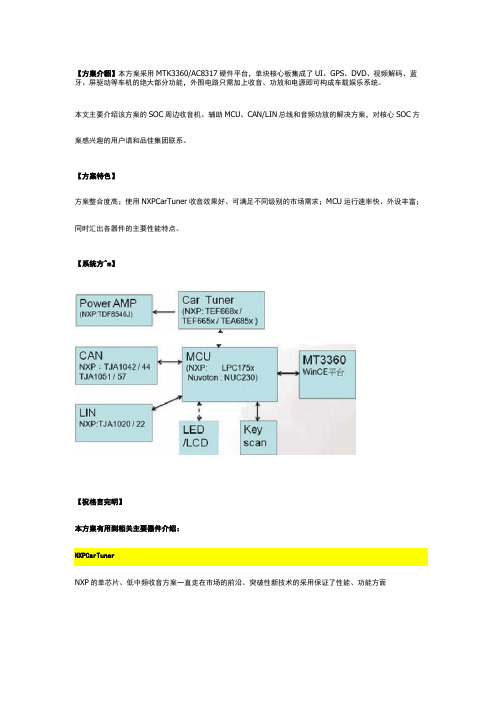
【方案介貂】本方案采用MTK3360/AC8317硬件平台,单块核心板集成了UI、GPS、DVD、视频解码、蓝牙、屏驱动等车机的绝大部分功能,外围电路只需加上收音、功放和电源即可构成车载娱乐系统。
本文主要介绍该方案的SOC周边收音机、辅助MCU、CAN/LIN总线和音频功放的解决方案,对核心SOC方案感兴趣的用户请和品佳集团联系。
【方案特色】方案整合度高;使用NXPCarTuner收音效果好、可满足不同级别的市场需求;MCU运行速率快、外设丰富;同时汇出各器件的主要性能特点。
【系统方^m】【祝格言完明】本方案有用到相关主要器件介绍:NXP的单芯片、低中频收音方案一直走在市场的前沿。
突破性新技术的采用保证了性能、功能方面iCccrn&olurd的领先,集成度不断提高使得开发变得更为简单,PCB 空间逐步减小,整体成本也在不断降低。
如TEF668x 、TEF665x 、TEA685x 三系列收音芯片管脚兼容,性能从高到低全面覆盖,可使产品形成高中低搭配,方便客户的选择。
下面分别介绍:1.NXPTEF668x(Lithio)系歹UTEF668x 低中频调谐器高性能单芯片是单芯片无线电IC ,包括AM/FM 无线电调谐器和软件定义的无线电信号处理。
它们扩展了恩智浦半导体广泛的、行业成熟的汽车无线电单调谐器产品组合,提供出色的无线电性能、最广泛的功能和最先进的软件算法,同时优化了系统成本。
HVQFN 封装占用最小的PCB 空间,并适用于双层和多层PCB 。
无线电接收器包括最高功能集、AM/FM 前端、调谐合成器、信道过滤、FM 信道均衡、FM 多路改善、解调、FM 立体声解码、弱信号处理、噪声抑制和RDS ,并提供与DARC 解调器/解码器的接口。
功能框图:□CO DlYidersFM&PFFM tronLendTEF6G8XAM BFF AM froniendRadto ProM&singAudie □ACDig..!alrMn ^efface12sMp 证I^OuEputbufferbuff&rXTAL3sdllatorDigitalTuRiitgSYstemADC功能特点:•包含调谐器和软件定义无线电处理的免校准数字接收器•基于命令的高级用户接口,兼具高度控制灵活性和易控性。
Micrel KSZ8851-16MLL 48-pin单端口以太网控制器与非PCI接口评估板用户指南

KSZ8851-16MLL48-pin Single-Port Ethernet ControllerWith 8-bit or 16-bit Non-PCI InterfaceEvaluation Board User’s GuideRevision 1.1August 2010© Micrel, Inc. 2007All rights reservedMicrel is a registered trademark of Micrel and its subsidiaries in theUnited States and certain other countries. All other trademarks are theproperty of their respective owners.The information furnished by Micrel in this datasheet is believed to be accurate and reliable. However, no responsibility is assumed by Micrel for its use. Micrel reserves the right to change circuitry and specifications at any time without notification to the customer. Micrel Products are not designed or authorized for use as components in life support appliances, devices or systems where malfunction of a product can reasonably be expected to result in personal injury. Life support devices or systems are devices or systems that (a) are intended for surgical implant into the body or (b) support or sustain life, and whose failure to perform can be reasonably expected to result in a significant injury to the user.Micrel, Inc. August 6, 2010A Purchaser's use or sale of Micrel Products for use in life support appliances, devices or systems is at Purchaser's own risk and Purchaser agrees to fully indemnify Micrel for any damages resulting from such use or sale.Revision HistoryRevisionDateSummary of Changes1.0 2/20/2008 Initial Release1.1 8/6/2010Add JP8 for connection between VDD_IO and 1.8V (if VDD_IO is 1.8V). Changed the LED pulled up to 3.3V.Table of Contents1.0Introduction (5)2.0Board Features (5)3.0Evaluation Kit Contents (5)4.0Hardware Description (6)4.1Host Interface (7)4.2Jumper Setting & Definition (8)4.3Power Supply and Test Point Definition (9)4.4RJ-45 Connector and Transformer (9)4.5EEPROM and LED Indicators (9)4.6Board Reset (10)5.0Bill of Materials (11)Micrel, Inc. August 6, 2010List of FiguresFigure 1. KSZ8851-16MLL Evaluation Board (6)Figure 2. KSZ8851-16MLL-Eval Host Interface Connection with Spirent SmartBits (7)List of TablesTable 1. Header JP1 – Host Interface Connection for SD[15:0] (7)Table 2. Header JP1 – Host Interface Connection for Control and Power (8)Table 3. KSZ8851-16MLL-Eval Jumper Definition (8)Table 4. KSZ8851-16MLL-Eval Test Point Definition (9)Table 5. KSZ8851-16MLL EEPROM Format (9)Table 6. KSZ8851-16MLL-Eval Port Status LED Definition (10)Table 7. KSZ8851-16MLL-Eval LED Definition (10)Micrel, Inc. August 6, 20101.0 IntroductionThe KSZ8851-16MLL-Eval Evaluation Board is intended to provide a convenient and fast way to evaluate or demonstrate the functionality and performance of this new Single-Port Ethernet Controller KSZ8851-16MLL device from Micrel.The KSZ8851-16MLL comes with a 48-pin, lead-free LQFP (7mm x 7mm) package and provides an ideal solution for applications requiring high-performance from single-port Ethernet Controller with 8-bit or 16-bit generic processor interface. The KSZ8851-16MLL offers the most cost-effective solution for adding high-throughput Ethernet connectivity to traditional embedded systems.This evaluation board is designed as a stand alone without microcontroller or M16C on board. By default the KSZ8851-16MLL-Eval board comes with an operation of 16-bit bus mode, Little Endian mode and disabled EEPROM for KSZ8851-16MLL device. Customer may wire the board for his desired interface. The purpose is to provide a simple tool that can be used to evaluate the KSZ8851-16MLL device by connecting via headers to customer provided Microcontroller or Non-PCI hardware platform.Micrel provides a basic software driver based on the 8 or 16-bit bus solution and different operating system platforms to evaluate the KSZ8851-16MLL functionality and performance. The software includes a configuration utility to allow quick and easy device setup, initialization and transmit/receive packet. All KSZ8851-16MLL configuration pins and host interface signals are accessible either by jumpers, test points or headers.2.0 Board Features•One KSZ8851-16MLL 48-pin Single-Port Ethernet Controller with shared data bus for host interface•Single +5V/GND power input from headers•RJ-45 Jack for Fast Ethernet cable interface•HP Auto-MDIX for automatic detection and correction for straight-through and crossover cables•Two on board LDO voltage regulators, one for VDD_IO and the other for VDD_A3.3•One AT93C46 for external EEPROM interface•Two LED indicators for port status and activity•One LED indicator for 3.3V output ready•One LED indicator for Power Management Event (PME) output status•Jumpers to configure strapping pins and VDD_IO voltage option•Headers to wire the host interface from external hardware platform•Manual reset button for quick reboot after re-configuration of strapping pins3.0 Evaluation Kit ContentsThe KSZ8851-16MLL Evaluation Kit includes the following hardware:•KSZ8851-16MLL Evaluation BoardThe KSZ8851-16MLL Data Sheet and Hardware Design Package with the following collaterals that can be downloaded from Micrel’s website at •KSZ8851-16MLL Eval Board Schematic (PDF and OrCAD DSN file)•KSZ8851-16MLL Eval Board Gerber File (PDF version included)•KSZ8851-16MLL Eval Board User’s Guide (this document and included BOM)•KSZ8851-16MLL IBIS ModelMicrel, Inc. August 6, 20104.0 Hardware DescriptionThe KSZ8851-16MLL-Eval (shown in Figure 1) comes in a compact form factor and plugs directly into industry standard test equipment such as Spirent SmartBits, the other side of board is wired to external host interface through headers. Configuration of the KSZ8851-16MLL is accomplished through on-board jumper selections and/or by register access via the host shared data/control bus Interface.Figure 1. KSZ8851-16MLL Evaluation Board (Rev 1.1)Other features include a RJ-45 Jack for Fast Ethernet cable connection, transformer (Pulse H1102) to block DC level and provide a true AC coupling, EEPROM (Atmel AT93C46) to load MAC address when it is enabled, jumper to select LDO output for VDD_IO voltage, programmable LED indicators for reporting port link status and activity, and a manual reset button for quick reboot after re-configuration of strapping pins.The KSZ8851-16MLL-Eval receives +5V DC input power supply from its Headers JP1.Micrel, Inc. August 6, 2010Micrel, Inc. August 6, 20104.1 Host InterfaceThe KSZ8851-16MLL-Eval board receives +5V power from the header JP1 (pin 1/3). Figure 2 shows the Host interface connection with Spirent SmartBits for system set-up and performance test.Figure 2. KSZ8851-16MLL-Eval Host Interface Connection with Spirent SmartBitsThe KSZ8851-16MLL-Eval has a 40-pin header (JP1) for Host interface to external any Non-PCI hardware platform. Table 1 lists Shared Data SD[15:0] pin outs for the Host interface on header JP1. Table 2 lists the rest of control signals and power/ground pin outs for the Host interface on header JP1.16-Bit Bus Mode (pin 1 pull-up) 8-Bit Bus Mode (pin 1 pull down) Pin # (JP1) Shared Data Bus Signal CMD = 0 (low) CMD = 1 (high) CMD = 0 (low) CMD = 1 (high) 20 SD0 D0 x (don’t care) D0 A0 19SD1D1 x (don’t care) D1 A1 18 SD2 D2 A2 D2 A2 17 SD3 D3 A3 D3 A3 16 SD4 D4 A4 D4 A4 15 SD5 D5 A5 D5 A5 14 SD6 D6 A6 D6 A6 13 SD7 D7 A7 D7 A7 12 SD8 D8 x (don’t care) GND GND 11 SD9 D9 x (don’t care) GND GND 10 SD10 D10 x (don’t care) GND GND 9SD11D11 x (don’t care) GND GND 8 SD12 D12 BE0 GND GND 7 SD13 D13 BE1 GND GND 6 SD14 D14 BE2 GND GND 5 SD15D15BE3GNDGNDTable 1. Header JP1 – Host Interface Connection for SD[15:0]Pin # (JP1) Power & ControlSignal NamesDescription1, 3 5.0V_IN +5V power supply inputs for this board 2, 4, 21, 22, 25,26, 29, 33, 34, 37, 38, 39, 40 GND Groundinputs/pins23 CPU_CSN Chip Select input from host CPU24 CPU_RSTN Reset input from host CPU27 CPU_PME Power Management Event output to host CPU28 CPU_CMD Command type input from host CPU31 CPU_INTRN Interrupt output to host CPU35 CPU_WRN Write input from host CPU36 CPU_RDN Read input from host CPU30, 32 Spares For customer to useTable 2. Header JP1 – Host Interface Connection for Control and Power4.2 Jumper Setting & DefinitionThe KSZ8851-16MLL-Eval does not require any jumper for normal operation except the VDD_IO option. During power-up, the KSZ8851-16MLL is configured using the chip’s internal pull-up and pull-down resistors with its default strapping pin values which will set this device in operation of 16-bit bus mode, little endian and without EEPROM. Jumpers are provided to override the default settings, allowing for quick configuration and re-configuration of the board. To override the default settings, simply select and close the desired jumper setting(s) and toggle the on-board manual reset button (S1) for the new setting(s) to take effect.The KSZ8851-16MLL-Eval jumper settings are defined in Table 3 below.Jumper Definition Setting DescriptionJP2 EED_IO OFF (Default) OFF: EEPROM is not presentON: EEPROM is presentJP3 3.3V ON (Default) ON: to select 3.3V for VDD_IO (JP5 and JP6 must be OFF)OFF: De-select 3.3VJP4 EESK OFF (Default) OFF: Little EndianON: Big EndianJP5 2.5V OFF (Default) ON: to select 2.5V for VDD_IO (JP3 and JP6 must be OFF)OFF: De-select 2.5VJP6 1.8V OFF (Default) ON: to select 1.8V for VDD_IO (JP3 and JP5 must be OFF)OFF: De-select 1.8VJP7 P1LED1 OFF (Default) OFF: 16-Bit bus modeON: 8-Bit bus modeJP8 VDD_IO OFF (Default) OFF: VDD_IO = 2.5V or 3.3VON: VDD_IO = 1.8VTable 3. KSZ8851-16MLL-Eval Jumper DefinitionMicrel, Inc. August 6, 2010Power Supply and Test Point DefinitionThe KSZ8851-16MLL-Eval is supplied from external +5.0V DC power through a jumper (pin 1 and 3 at JP1), this +5.0V DC input is converted to both +3.3V with a Micrel LDO voltage regulator (U3, MIC5209BM) for VDD_A3.3 analog power and VDD (option for 3.3V, 2.5V or 1.8V) with a Micrel LDO voltage regulator (U5, MIC5209BM) for VDD_IO digital power. The KSZ8851-16MLL contains an internal +1.8V LDO, to provide its core, analog and PLL voltages.The KSZ8851-16MLL-Eval has four test points. They are defined in the following Table 4.Test Point DefinitionTP1 Power supply measurement for VDD_IOTP2 Power supply measurement for VDD_A3.3TP3 1.8V digital core voltage output measurement fromKSZ8851-16MLL internal LDOTP4 External power supply 5.0V_IN measurementTable 4. KSZ8851-16MLL-Eval Test Point Definition4.3 RJ-45 Connector and TransformerThe RJ-45 Jack (J1) connects to standard CAT-5 Ethernet cable to interface with 10Base-T/100Base-TX Ethernet devices. The LAN interface on the KSZ8851-16MLL is connected to a transformer (T1) with 50 ohm termination resistors for both TX+/- and RX+/- differential pairs. The line side of the transformer is connected to the RJ-45 connectors (J1).J1 also supports Auto-MDIX and Auto-Negotiation / Forced Modes.4.4 EEPROM and LED IndicatorsIt is optional in the KSZ8851-16MLL to use an external EEPROM. The EED_IO (JP2) must be pulled high (ON) to use external EEPROM.An external serial EEPROM with a standard microwire bus interface is used for non-volatile storage of information such as the host MAC address. The KSZ8851-16MLL can detect if the EEPROM is either a 1KB (93C46) or 4KB (93C66) EEPROM device. The EEPROM must be organized as 16-bit mode.The KSZ8851-16MLL EEPROM format is given in Table 5.WORD 15 8 7 00H Reserved1H Host MAC Address Byte 2 Host MAC Address Byte 12H Host MAC Address Byte 4 Host MAC Address Byte 33H Host MAC Address Byte 6 Host MAC Address Byte 54H – 6H Reserved7H-3FH Not used for KSZ8851-16MLL (available for user to use)Table 5. KSZ8851-16MLL EEPROM FormatMicrel, Inc. August 6, 2010A dual LED indicator (LED1) is located adjacent to the RJ-45 Connector (J1). The top LED is connected to P1LED1 (pin 1) and bottom LED is connected to P1LED0 (pin 2) of the KSZ8851-16MLL.The two LEDs are programmable to LED mode ‘0’ or ‘1’ via register 0xC6 bits [9], and are defined in the following Table 6.LED Mode0 (Default) 1LED1 (Top) 100BT ACTLED1 (Bottom) LINK/ACT LINKTable 6. KSZ8851-16MLL-Eval Port Status LED DefinitionTable 7 shows the rest of LEDs definition.LED Color DescriptionLED2 Green Power Management Event (PME) StatusLED3 Red 3.3V Power available indicatorTable 7. KSZ8851-16MLL-Eval LED Definition4.5 Board ResetThe KSZ8851-16MLL-Eval generates a reset signal from the reset circuitry during power up. It also provides a push button S1 reset circuit to reset the KSZ8851-16MLL device. During power up, the board is automatically reset. User can also press reset button S1 on the board for a manual reset.Micrel, Inc. August 6, 2010KSZ8851-16MLL-Eval Evaluation Board User’s Guide Rev. 1.1 Micrel, Inc.August 6, 201011/11 5.0 Bill of MaterialsKSZ8851-16MLL Eval Board (Revision 1.1)。
MSM8939核心板项目规格书

I2S NFC 指纹模块接 口 摄像头闪光 灯控制接口 环境光传感 器接口 电池接口 USB MIC EAR Output SPEAKER 耳机
为外挂回声抑制预留 NFC 接口
SPI 总线指纹模块接口
支持
1 1 2 路,开关切换 双路 1 路差分输出 1 路,0.8W max 1路 12+(不用的引脚复用可增加
27 28 30
PRI_MIC_GND PRI_MIC_P MIC_BIAS1
AUDIO AUDIO AUDIO
主 MIC 参考地 主 MIC 输入信号 MIC 偏压 1.8v
主 MIC 地
不要接外围 主地,直接 31 32 33 34 SEC_MIC_GND SEC_MIC_P SPKR_OUT_M SPKR_OUT_P AUDIO AUDIO AUDIO AUDIO 副 MIC 参考地 副 MIC 输入引脚 扬声器输出 M 扬声器输出 P 不要接外围 主地,直接 35 36 37 38 39 40 42 43 44 GND_HEADSET EAR_OUT_M EAR_OUT_P CDC_HPH_L CDC_HPH_R MIC_P_HSET BLSP3_CS1_N PS_HOLD_PMIC_TP LED_R_DRV AUDIO GND AUDIO AUDIO AUDIO AUDIO AUDIO SPI DEBUG PIN LED_DRV 耳机参考地 earpice 输出 M earpice 输出 P 耳机左声道输出 耳机右声道输出 耳机 mic 输入 指纹/SPI 片选信号 1,SPI sdcard 时使用 PS_HOLD 调试引脚 5mA 1.8v logic 接耳机地 副 MIC 地
深圳元麦科技有限公司
WCDMA Band Standard CDMA Band Standard GSM BAND Standard WLAN/BT/ FM 802.11a/b/g/n/ac WLAN WIFI 热点 Bluetooth 4.0 FM 支持 支持 RX 2.4G & 5.8G supported 支持 GSM 850/900/1800/1900; follow 3GPP spec CDMA 1x&EVDO 800; follow 3GPP spec WCDMA 850/900/1900/2100; follow 3GPP spec
3386电位器

*RoHS Directive 2002/95/EC Jan 27 2003 including Annex. Fluorinert is a registered trademark of 3M Co.Specifications are subject to change without notice.Customers should verify actual device performance in their specific applications.ModelStyleStandard or Modified Product Indicator-1 = Standard Product -EY5 = Extended Shaft Resistance Code Optional Suffix LetterT =Knob**Packaging DesignatorBlank =Tube (Standard)R =T ape & Reel (W and U Pin Styles Only)A =Ammo Pack (W and U Pin Styles Only)TerminationsLF =100 % Tin-plated (RoHS compliant)Blank =90 % Tin / 10 % Lead-plated(Standard)**Knob option is available only in standard Tube packaging.Consult factory for other available options.Electrical Characteristics Standard Resistance Range..................................10 to 2 megohms(see standard resistance table)Resistance Tolerance............±10 % std.(tighter tolerance available)Absolute Minimum Resistance.........................................2 ohms max.Contact Resistance Variation.............................2 % or 3 ohms max.(whichever is greater)AdjustabilityVoltage....................................±0.05 %Resistance..............................±0.15 %Resolution.....................................Infinite Insulation Resistance................500 vdc.1,000 megohms min.Dielectric StrengthSea Level .................................900 vac 70,000 Feet..............................350 vac Adjustment Angle..................280 °nom.Environmental Characteristics Power Rating (300 volts max.)85 °C........................................0.5 watt 125 °C.........................................0 watt Temperature Range....-55 °C to +125 °C Temperature Coefficient....±100 ppm/°C Seal Test........................85 °C Fluorinert †-STD-202 Method 10396 hours(2 % ∆TR, 10 Megohms min.)Vibration.........30 G (1 % ∆TR; 1 % ∆VR)Shock...........100 G (1 % ∆TR; 1 % ∆VR)Load Life ..1,000 hours 0.5 watt @ 70 °C(3 % ∆TR; 1 % or 1 ohm,whichever is greater, CRV)Rotational Life........................200 cycles(4 % ∆TR; 1 % or 1 ohm,whichever is greater, CRV)Physical CharacteristicsMechanical Angle..................310 °nom.Torque .............................5.0 oz-in. max.Stop Strength................15.0 oz -in. min.Terminals........................Solderable pins Weight ........................................0.03 oz.Marking...........................Manufacturer’strademark, resistance code,wiring diagram, date code,manufacturer’s modelnumber and styleFlammability...........................U.L. 94V-0Standard Packaging.....50 pcs. per tube Wiper................50 % (Actual TR) ±10 %Adjustment Tool..............................H-90.76(.030) .76(.030)3.15(.124)X X Resistance Resistance (Ohms)Code 1010020200505001001012002015005011,0001022,0002025,00050210,00010320,00020325,00025350,000503100,000104200,000204250,000254500,0005041,000,0001052,000,000205Standard Resistance TablePopular distribution resistance values listed in boldface. Special resistances available.*Ro H S C O M P L I A N T V E R S I O N S A V A I L A B L ESpecifications are subject to change without notice.Customers should verify actual device performance in their specific applications.The Model 3386 is available with a knob for finger adjustment. Add suffix letter "T" to order code for F , P and X terminal styles.ADJ. SLOT 5.59(.220) 1.02(.040) 1.40(.055) WIDE DEEPLONG ADJ. SLOT 3386H-EY53386X-EY5 – SHOWNCLOCKWISEDIMENSIONS ARE:MM (INCHES)TOLERANCES: ±0.25 (.010) EXCEPT WHERE NOTEDSpecifications are subject to change without notice.Customers should verify actual device performance in their specific applications.REV. 02/06SIDE ADJUST 3386W-1TOP ADJUST 3386U-1Packaging SpecificationsMeets EIA Specification 468.。
电压检测单片机复位监控芯片

符号 Vcc PD
TOPR Tstg
范围 0.3~+15.0
400 350 30~+75 55~+150
单位 V mW
Type No. KIA7733S KIA7734S KIA7735S KIA7736S KIA7739S KIA7742S KIA7745S
Marking 77J 77K 77L 77M 77N 77P 77R
MILLIMETERS 4.70 MAX 4.80 MAX 3.70 MAX 0.45 1.00 1.27 0.55 0.45 14.00+0.50 0.55 MAX 2.30 0.45 MAX 1.00
K FF
123
DIM MILLIMETERS
A
4.70 MAX
B
2.50+0.2
C
1.70 MAX
电气特性
特性
检 测 电 压
低电平输出电压 输出漏电流 滞后电压
检测电压温度系数
测 符号 试
CIR
VS
1
VOL
1
IOH
1
⊿VS
1
VS/⊿T 1
测试条件
KIA7719P/S
KIA7721P/S
KIA7723P/S
KIA7725P/S
KIA7727P/S
KIA7729P/S
RL=200 VOL 0.4V
KIA7731P/S KIA7732P/S KIA7733P/S
注 1 连接 LED 和 R2 即可得到欠电指示器 2 连接并调整 C1 和 R1 选择不同的上电延时时间
使用注意事项
焊接 扁平封装 SOT-89 封装 元器件的种类越来越多 元器件的封装技术也日趋多样化 尤其是表面装贴元件正逐步渗透到工业 的各个方面 已经成了世界范围内流行的趋势 虽然在焊接过程中元件不可避免的要暴露在高温之下 我们推荐限制焊接的温度到较低温度 如下图所示 以保持元件的可靠性
全面射频IC EDA及测试工具方案介绍
提参建模:生成 PDK model 文件,完美表征成熟半导体工艺线 设计仿真:MMIC,RFIC,电路级设计,电磁和热分析,封装模拟 电路测试:片上测试,封装后测试;
射频芯片,模拟芯片,数字芯片
Electro-thermal
是德科技 芯片测试宝典
及其他半导体IC 数字芯片测试 ...................................................................................... 04 技术概述 .................................................................................................................. 04 手机 baseband ....................................................................................................... 08
FROM MODELING,
SIMULATION TO TEST
覆盖IC全产业链,是德科技提供最 全面IC EDA及测试工具
Start IC Specs
是德科技(原安捷伦电子测量事业部),不仅是世界上最大的硬 件电子测试测量仪器公司,也是 RFIC design EDA 软件 ADS 的 生产厂商。我们提供大量的软件,硬件,覆盖 IC 全产业链测试 与仿真需求。
-编解码器逻辑测试 .......................................................
常用开关电源芯片大全之欧阳育创编

常用开关电源芯片大全第1章DC-DC电源转换器/基准电压源1.1 DC-DC电源转换器1.低噪声电荷泵DC-DC电源转换器AAT3113/AAT31142.低功耗开关型DC-DC电源转换器ADP30003.高效3A开关稳压器AP15014.高效率无电感DC-DC电源转换器FAN56605.小功率极性反转电源转换器ICL76606.高效率DC-DC电源转换控制器IRU30377.高性能降压式DC-DC电源转换器ISL64208.单片降压式开关稳压器L49609.大功率开关稳压器L4970A10.1.5A降压式开关稳压器L497111.2A高效率单片开关稳压器L497812.1A高效率升压/降压式DC-DC电源转换器L597013.1.5A降压式DC-DC电源转换器LM157214.高效率1A降压单片开关稳压器LM1575/LM2575/LM2575HV15.3A降压单片开关稳压器LM2576/LM2576HV16.可调升压开关稳压器LM257717.3A降压开关稳压器LM259618.高效率5A开关稳压器LM267819.升压式DC-DC电源转换器LM2703/LM270420.电流模式升压式电源转换器LM273321.低噪声升压式电源转换器LM275022.小型75V降压式稳压器LM500723.低功耗升/降压式DC-DC电源转换器LT107324.升压式DC-DC电源转换器LT161525.隔离式开关稳压器LT172526.低功耗升压电荷泵LT175127.大电流高频降压式DC-DC电源转换器LT176528.大电流升压转换器LT193529.高效升压式电荷泵LT193730.高压输入降压式电源转换器LT195631.1.5A升压式电源转换器LT196132.高压升/降压式电源转换器LT343333.单片3A升压式DC-DC电源转换器LT343634.通用升压式DC-DC电源转换器LT346035.高效率低功耗升压式电源转换器LT346436.1.1A升压式DC-DC电源转换器LT346737.大电流高效率升压式DC-DC电源转换器LT378238.微型低功耗电源转换器LTC175439.1.5A单片同步降压式稳压器LTC187540.低噪声高效率降压式电荷泵LTC191141.低噪声电荷泵LTC3200/LTC3200-542.无电感的降压式DC-DC电源转换器LTC325143.双输出/低噪声/降压式电荷泵LTC325244.同步整流/升压式DC-DC电源转换器LTC340145.低功耗同步整流升压式DC-DC电源转换器LTC340246.同步整流降压式DC-DC电源转换器LTC340547.双路同步降压式DC-DC电源转换器LTC340748.高效率同步降压式DC-DC电源转换器LTC341649.微型2A升压式DC-DC电源转换器LTC342650.2A两相电流升压式DC-DC电源转换器LTC342851.单电感升/降压式DC-DC电源转换器LTC344052.大电流升/降压式DC-DC电源转换器LTC344253.1.4A同步升压式DC-DC电源转换器LTC345854.直流同步降压式DC-DC电源转换器LTC370355.双输出降压式同步DC-DC电源转换控制器LTC373656.降压式同步DC-DC电源转换控制器LTC377057.双2相DC-DC电源同步控制器LTC380258.高性能升压式DC-DC电源转换器MAX1513/MAX151459.精简型升压式DC-DC电源转换器MAX1522/MAX1523/MAX152460.高效率40V升压式DC-DC电源转换器MAX1553/MAX155461.高效率升压式LED电压调节器MAX1561/MAX159962.高效率5路输出DC-DC电源转换器MAX156563.双输出升压式DC-DC电源转换器MAX1582/MAX1582Y64.驱动白光LED的升压式DC-DC电源转换器MAX158365.高效率升压式DC-DC电源转换器MAX1642/MAX164366.2A降压式开关稳压器MAX164467.高效率升压式DC-DC电源转换器MAX1674/MAX1675/MAX167668.高效率双输出DC-DC电源转换器MAX167769.低噪声1A降压式DC-DC电源转换器MAX1684/MAX168570.高效率升压式DC-DC电源转换器MAX169871.高效率双输出降压式DC-DC电源转换器MAX171572.小体积升压式DC-DC电源转换器MAX1722/MAX1723/MAX172473.输出电流为50mA的降压式电荷泵MAX173074.升/降压式电荷泵MAX175975.高效率多路输出DC-DC电源转换器MAX180076.3A同步整流降压式稳压型MAX1830/MAX183177.双输出开关式LCD电源控制器MAX187878.电流模式升压式DC-DC电源转换器MAX189679.具有复位功能的升压式DC-DC电源转换器MAX194780.高效率PWM降压式稳压器MAX1992/MAX199381.大电流输出升压式DC-DC电源转换器MAX61882.低功耗升压或降压式DC-DC电源转换器MAX62983.PWM升压式DC-DC电源转换器MAX668/MAX66984.大电流PWM降压式开关稳压器MAX724/MAX72685.高效率升压式DC-DC电源转换器MAX756/MAX75786.高效率大电流DC-DC电源转换器MAX761/MAX76287.隔离式DC-DC电源转换器MAX8515/MAX8515A88.高性能24V升压式DC-DC电源转换器MAX872789.升/降压式DC-DC电源转换器MC33063A/MC34063A90.5A升压/降压/反向DC-DC电源转换器MC33167/MC3416791.低噪声无电感电荷泵MCP1252/MCP125392.高频脉宽调制降压稳压器MIC220393.大功率DC-DC升压电源转换器MIC229594.单片微型高压开关稳压器NCP1030/NCP103195.低功耗升压式DC-DC电源转换器NCP1400A96.高压DC-DC电源转换器NCP140397.单片微功率高频升压式DC-DC电源转换器NCP141098.同步整流PFM步进式DC-DC电源转换器NCP142199.高效率大电流开关电压调整器NCP1442/NCP1443/NCP1444/NCP1445100.新型双模式开关稳压器NCP1501101.高效率大电流输出DC-DC电源转换器NCP1550102.同步降压式DC-DC电源转换器NCP1570103.高效率升压式DC-DC电源转换器NCP5008/NCP5009 104.大电流高速稳压器RT9173/RT9173A105.高效率升压式DC-DC电源转换器RT9262/RT9262A106.升压式DC-DC电源转换器SP6644/SP6645107.低功耗升压式DC-DC电源转换器SP6691108.新型高效率DC-DC电源转换器TPS54350109.无电感降压式电荷泵TPS6050x110.高效率升压式电源转换器TPS6101x111.28V恒流白色LED驱动器TPS61042112.具有LDO输出的升压式DC-DC电源转换器TPS6112x 113.低噪声同步降压式DC-DC电源转换器TPS6200x114.三路高效率大功率DC-DC电源转换器TPS75003115.高效率DC-DC电源转换器UCC39421/UCC39422116.PWM控制升压式DC-DC电源转换器XC6371117.白光LED驱动专用DC-DC电源转换器XC9116118.500mA同步整流降压式DC-DC电源转换器XC9215/XC9216/XC9217119.稳压输出电荷泵XC9801/XC9802120.高效率升压式电源转换器ZXLB16001.2 线性/低压差稳压器121.具有可关断功能的多端稳压器BAXXX122.高压线性稳压器HIP5600123.多路输出稳压器KA7630/KA7631124.三端低压差稳压器LM2937125.可调输出低压差稳压器LM2991126.三端可调稳压器LM117/LM317127.低压降CMOS500mA线性稳压器LP38691/LP38693128.输入电压从12V到450V的可调线性稳压器LR8129.300mA非常低压降稳压器(VLDO)LTC3025130.大电流低压差线性稳压器LX8610131.200mA负输出低压差线性稳压器MAX1735132.150mA低压差线性稳压器MAX8875133.带开关控制的低压差稳压器MC33375134.带有线性调节器的稳压器MC33998135.1.0A低压差固定及可调正稳压器NCP1117136.低静态电流低压差稳压器NCP562/NCP563137.具有使能控制功能的多端稳压器PQxx138.五端可调稳压器SI-3025B/SI-3157B139.400mA低压差线性稳压器SPX2975140.五端线性稳压器STR20xx141.五端线性稳压器STR90xx142.具有复位信号输出的双路输出稳压器TDA8133143.具有复位信号输出的双路输出稳压器TDA8138/TDA8138A144.带线性稳压器的升压式电源转换器TPS6110x145.低功耗50mA低压降线性稳压器TPS760xx146.高输入电压低压差线性稳压器XC6202147.高速低压差线性稳压器XC6204148.高速低压差线性稳压器XC6209F149.双路高速低压差线性稳压器XC64011.3 基准电压源150.新型XFET基准电压源ADR290/ADR291/ADR292/ADR293151.低功耗低压差大输出电流基准电压源MAX610x152.低功耗1.2V基准电压源MAX6120153.2.5V精密基准电压源MC1403154.2.5V/4.096V基准电压源MCP1525/MCP1541155.低功耗精密低压降基准电压源REF30xx/REF31xx156.精密基准电压源TL431/KA431/TLV431A第2章AC-DC转换器及控制器1.厚膜开关电源控制器DP104C2.厚膜开关电源控制器DP308P3.DPA-Switch系列高电压功率转换控制器DPA423/DPA424/DPA425/DPA4264.电流型开关电源控制器FA13842/FA13843/FA13844/FA138455.开关电源控制器FA5310/FA53116.PWM开关电源控制器FAN75567.绿色环保的PWM开关电源控制器FAN76018.FPS型开关电源控制器FS6M07652R9.开关电源功率转换器FS6Sxx10.降压型单片AC-DC转换器HV-2405E11.新型反激准谐振变换控制器ICE1QS0112.PWM电源功率转换器KA1M088013.开关电源功率转换器KA2S0680/KA2S088014.电流型开关电源控制器KA38xx15.FPS型开关电源功率转换器KA5H0165R16.FPS型开关电源功率转换器KA5Qxx17.FPS型开关电源功率转换器KA5Sxx18.电流型高速PWM控制器L499019.具有待机功能的PWM初级控制器L599120.低功耗离线式开关电源控制器L659021.LINK SWITCH TN系列电源功率转换器LNK304/LNK305/LNK30622.LINK SWITCH系列电源功率转换器LNK500/LNK501/LNK52023.离线式开关电源控制器M51995A24.PWM电源控制器M62281P/M62281FP25.高频率电流模式PWM控制器MAX5021/MAX502226.新型PWM开关电源控制器MC4460427.电流模式开关电源控制器MC4460528.低功耗开关电源控制器MC4460829.具有PFC功能的PWM电源控制器ML482430.液晶显示器背光灯电源控制器ML487631.离线式电流模式控制器NCP120032.电流模式脉宽调制控制器NCP120533.准谐振式PWM控制器NCP120734.低成本离线式开关电源控制电路NCP121535.低待机能耗开关电源PWM控制器NCP123036.STR系列自动电压切换控制开关STR8xxxx37.大功率厚膜开关电源功率转换器STR-F665438.大功率厚膜开关电源功率转换器STR-G865639.开关电源功率转换器STR-M6511/STR-M652940.离线式开关电源功率转换器STR-S5703/STR-S5707/STR-S570841.离线式开关电源功率转换器STR-S6401/STR-S6401F/STR-S6411/STR-S6411F 442.开关电源功率转换器STR-S651343.离线式开关电源功率转换器TC33369~TC3337444.高性能PFC与PWM组合控制集成电路TDA16846/TDA1684745.新型开关电源控制器TDA1685046.“绿色”电源控制器TEA150447.第二代“绿色”电源控制器TEA150748.新型低功耗“绿色”电源控制器TEA153349.开关电源控制器TL494/KA7500/MB375950.Tiny SwitchⅠ系列功率转换器TNY253、TNY254、TNY25551.Tiny SwitchⅡ系列功率转换器TNY264P~TNY268G52.TOP Switch(Ⅱ)系列离线式功率转换器TOP209~TOP22753.TOP Switch-FX系列功率转换器TOP232/TOP233/TOP23454.TOP Switch-GX系列功率转换器TOP242~TOP25055.开关电源控制器UCX84X56.离线式开关电源功率转换器VIPer12AS/VIPer12ADIP57.新一代高度集成离线式开关电源功率转换器VIPer53第3章功率因数校正控制/节能灯电源控制器1.电子镇流器专用驱动电路BL83012.零电压开关功率因数控制器FAN48223.功率因数校正控制器FAN75274.高电压型EL背光驱动器HV8265.EL场致发光背光驱动器IMP525/IMP5606.高电压型EL背光驱动器/反相器IMP8037.电子镇流器自振荡半桥驱动器IR21568.单片荧光灯镇流器IR21579.调光电子镇流器自振荡半桥驱动器IR215910.卤素灯电子变压器智能控制电路IR216111.具有功率因数校正电路的镇流器电路IR216612.单片荧光灯镇流器IR216713.自适应电子镇流器控制器IR252014.电子镇流器专用控制器KA754115.功率因数校正控制器L656116.过渡模式功率因数校正控制器L656217.集成背景光控制器MAX8709/MAX8709A18.功率因数校正控制器MC33262/MC3426219.固定频率电流模式功率因数校正控制器NCP165320.EL场致发光灯高压驱动器SP440321.功率因数校正控制器TDA4862/TDA486322.有源功率因数校正控制器UC385423.高频自振荡节能灯驱动器电路VK05CFL24.大功率高频自振荡节能灯驱动器电路VK06TL第4章充电控制器1.多功能锂电池线性充电控制器AAT36802.可编程快速电池充电控制器BQ20003.可进行充电速率补偿的锂电池充电管理器BQ20574.锂电池充电管理电路BQ2400x5.单片锂电池线性充电控制器BQ2401xB接口单节锂电池充电控制器BQ2402x7.2A同步开关模式锂电池充电控制器BQ241008.集成PWM开关控制器的快速充电管理器BQ29549.具有电池电量计量功能的充电控制器DS277010.锂电池充电控制器FAN7563/FAN756411.2A线性锂/锂聚合物电池充电控制器ISL629212.锂电池充电控制器LA5621M/LA5621V13.1.5A通用充电控制器LT157114.2A恒流/恒压电池充电控制器LT176915.线性锂电池充电控制器LTC173216.带热调节功能的1A线性锂电池充电控制器LTC173317.线性锂电池充电控制器LTC173418.新型开关电源充电控制器LTC198019.开关模式锂电池充电控制器LTC400220.4A锂电池充电器LTC400621.多用途恒压/恒流充电控制器LTC400822.4.2V锂离子/锂聚合物电池充电控制器LTC405223.可由USB端口供电的锂电池充电控制器LTC405324.小型150mA锂电池充电控制器LTC405425.线性锂电池充电控制器LTC405826.单节锂电池线性充电控制器LTC405927.独立线性锂电池充电控制器LTC406128.镍镉/镍氢电池充电控制器M62256FP29.大电流锂/镍镉/镍氢电池充电控制器MAX150130.锂电池线性充电控制器MAX150731.双输入单节锂电池充电控制器MAX1551/MAX155532.单节锂电池充电控制器MAX167933.小体积锂电池充电控制器MAX1736B接口单节锂电池充电控制器MAX181135.多节锂电池充电控制器MAX187336.双路输入锂电池充电控制器MAX187437.单节锂电池线性充电控制器MAX189838.低成本/多种电池充电控制器MAX190839.开关模式单节锂电池充电控制器MAX1925/MAX192640.快速镍镉/镍氢充电控制器MAX2003A/MAX200341.可编程快速充电控制器MAX712/MAX71342.开关式锂电池充电控制器MAX74543.多功能低成本充电控制器MAX846A44.具有温度调节功能的单节锂电池充电控制器MAX8600/MAX860145.锂电池充电控制器MCP73826/MCP73827/MCP7382846.高精度恒压/恒流充电器控制器MCP73841/MCP73842/MCP73843/MCP73844 647.锂电池充电控制器MCP73861/MCP7386248.单节锂电池充电控制器MIC7905049.单节锂电池充电控制器NCP180050.高精度线性锂电池充电控制器VM7205。
恩智浦 MIMXRT1020 EVK 开发板硬件用户指南说明书

© 2018 NXP B.V.MIMXRT1020 EVK Board Hardware User’sGuide1.IntroductionThis Hardware User’s Guide for the MIMXRT 1020Evaluation Kit (EVK) is based on the NXP Semiconductor i.MX RT1020 Processor. This board is fully supported by NXP Semiconductor. The guide includes system setup and debugging, and provides detailed information on overall design and usage of the EVK board from a hardware systems perspective.1.1. Board overviewThis EVK board is a platform designed to showcase the most commonly used features of the i.MX RT1020 Processor in a small, low cost package. The MIMXRT1020 EVK board is an entry level development board, which gives the developer the option of becoming familiar with the processor before investing a large amount or resources in more specific designs.NXP Semiconductors Document Number: MIMXRT1020EVKHUGUser's GuideRev. 0 , 05/2018Contents1.Introduction ........................................................................ 11.1.Board overview ....................................................... 11.2.MIMXRT1020 EVK contents ................................. 21.3.MIMXRT1020 EVK Board revision history ........... 32.Specifications ..................................................................... 32.1.i.MX RT1020 processor .......................................... 52.2.Boot Mode configurations ....................................... 52.3.Power tree ............................................................... 62.4.SDRAM memory .................................................... 92.5.SD Card slot ............................................................ 92.6.QSPI flash ............................................................... 92.7.Ethernet connector .................................................. B PHY connector ............................................. 102.9.Audio input / output connector .............................. 102.10.OpenSDA circuit (DAP-Link) ............................... 102.11.JTAG connector .................................................... 102.12.Arduino expansion port ......................................... er interface LED indicator ................................ 133.PCB information .............................................................. 134.EVK design files .............................................................. 135.Contents of the Evaluation Kit ......................................... 146.Revision history (14)IntroductionFeatures of the MIMXRT1020 EVK board are shown in Table 11.2. MIMXRT1020 EVK contentsThe MIMXRT1020 EVK contains the following items: •MIMXRT1020 EVK Board•USB Cable (Micro B)Specifications 1.3. MIMXRT1020 EVK Board revision history•Rev A: Prototype.2. SpecificationsThis chapter provides detailed information about the electrical design and practical considerations of the EVK Board, and is organized to discuss each block in the following block diagram of the EVK board.( Figure 1)Figure 1. Block diagramThe overview of the MIMXRT1020 EVK Board is shown in Figure 1 & Figure 2.SpecificationsFigure 2. Overview of the MIMXRT1020 EVK Board (Front side)Figure 3. Overview of the MIMXRT1020 EVK Board (Back side)Specifications 2.1. i.MX RT1020 processorThe i.MX RT1020 is a new processor family featuring NXP's advanced implementation of the Arm® Cortex®-M7 Core. It provides high CPU performance and best real-time response. The i.MX RT1020 provides various memory interfaces, including SDRAM, Raw NAND FLASH, NOR FLASH,SD/eMMC, Quad SPI, HyperBus and a wide range of other interfaces for connecting peripherals, such as WLAN, Bluetooth™, GPS. Same as other i.MX processors, i.MX RT1020 also has rich audio features, including SPDIF and I2S audio interface.The i.MX RT1020 applications processor can be used in areas such as industrial HMI, IoT, motor control and home appliances. The architecture's flexibility enables it to be used in a wide variety of other general embedded applications too. The i.MX processor provides all interfaces necessary to connectp eripherals such as WLAN, Bluetooth™, GPS.The more detail information about i.MX RT1020 can be found in the Datasheet and Reference Manual2.2. Boot Mode configurationsThe device has four boot modes (one is reserved for NXP’s use). The boot mode is selected based on the binary value stored in the internal BOOT_MODE register. Switch (SW8-3 & SW8-4) is used to select the boot mode on the MIMXRT1020 EVK Board.Typically, the internal boot is selected for normal boot, which is configured by external BOOT_CFG GPIOs. The following Table 3 shows the typical Boot Mode and Boot Device settings.NOTEFor more information about boot mode configuration, see the System Boot chapter of theMIMXRT1020 Reference Manual. (waiting for update)For more information about MIMXRT1020 EVK boot device selection and configuration, see the main board schematic. (waiting for update)Specifications2.3. Power treeA DC 5 V external power supply is used to supply the MIMXRT1020 EVK Board at J2, and a slide switch SW1 is used to turn the Power ON/OFF. J23 and J9 also can be used to supply the EVK Board. Different power supply need to configure different Jumper setting of J1. Table 4 shows the details:NOTEFor some computers’ USB, it cannot support 500ma before establishingcommunication. In this case, it is recommended to replace the computer oruse the power adapter(J2) to power the EVK Board.The power tree is shown in Figure 4SpecificationsFigure 4. Power TreeThe power control logic of the MIMXRT1020 EVK board is shown in the Figure 5: •It will power up SNVS, and then PMIC_REQ_ON will be switched on to enable external DC/DC to power up other power domains.•ON/OFF button is used to switch ON/OFF PMIC_REQ_ON to control power modes.•RESET button and WDOG output are used to reset the system power.SpecificationsFigure 5. Power Control Diagram The power rails on the board are shown in Table 5.Specifications2.4. SDRAM memoryOne 256 Mb, 166MHz SDRAM (MT48LC16M16A2P) is used on the EVK Board.2.5. SD Card slotThere is a SD card slot(J15) on the MIMXRT1020 EVK Board. J15 is the Micro SD slot for USDHC1 interface. If the developer wants to boot from the SD Card, the boot device switch (SW8) settings should be: OFF, ON, ON, OFF, as shown in Table 3.2.6. QSPI flashA 64 Mbit QSPI Flash is used on the MIMXRT1020 EVK Board. If the developer wants to boot from the QSPI Flash, the boot device switch(SW8) settings should be: OFF, OFF, ON, OFF, as shown in Table 3.2.7. Ethernet connectorThere is one Ethernet Mac controller in the MIMXRT1020 processor. The Ethernet subsystem of the MIMXRT1020 EVK Board is provided by the KSZ8081RNB 10/100M Ethernet Transceiver (U11) and a RJ45 (J14) with integrated Magnetic.Figure 6. Ethernet Connector RJ45Specifications2.8. USB PHY connectorThe MIMXRT1020 contains a integrated USB 2.0 PHYs capable of connecting to USB host/device systems at the USB low-speed (LS) rate of 1.5 Mbits/s, full-speed (FS) rate of 12 Mbits/s or at the USB 2.0 high-speed (HS) rate of 480 Mbits/s.2.9. Audio input / output connectorThe Audio CODEC used on the MIMXRT1020 EVK Board is Wolfson’s Low Power, high quality Stereo Codec, WM8960.The MIMXRT1020 EVK Board include one headphone interface (J11), one onboard MIC (P1), two speaker interfaces (J12, J13). J11 is a 3.5 mm audio stereo headphone jack, which supports jack detect.2.10. OpenSDA circuit (DAP-Link)The OpenSDA circuit (CMSIS–DAP) is an open-standard serial and debug adapter. It bridges serial and debug communications between a USB host and an embedded target processor.CMSIS-DAP features a mass storage device (MSD) bootloader, which provides a quick and easy mechanism for loading different CMSIS-DAP Applications such as flash programmers, run-control debug interfaces, serial-to-USB converters, and more. Two or more CMSIS-DAP applications can run simultaneously. For example, run-control debug application and serial-to-USB converter runs in parallel to provide a virtual COM communication interface while allowing code debugging via CMSIS-DAP with just single USB connection.For the MIMXRT1020 EVK Board, J23 is the connector between the USB host and the target processor. Jumper to serial downloader mode to use stable DAP-Link debugger function. If developer wants to make OpenSDA going to the bootloader mode, and press SW5 when power on. Meanwhile, the OpenSDA supports drag/drop feature for U-Disk. First, use the seral downloader mode and drag/drop the image file to U-Disk. Then select QSPI Flash as boot device and reset the Board, the image will run.2.11. JTAG connectorJ16 is a standard 20-pin/2.54 mm Box Header Connector for JTAG. The pin definitions are shown in Figure 7. Support SWD by default.SpecificationsFigure 7. JTAG pin definitions2.12. Arduino expansion portJ17 – J20 (unpopulated) is defined as Arduino Interface. The pin definitions of Arduino Interface are shown in Table 6.Specifications2.12.1. Power switchSW1 is a slide switch to control the power of the MIMXRT1020 EVK Board when the power supply is from J2. The function of this switch is listed below:•Sliding the switch to the ON position connects the 5 V power supply to the Evaluation board main power system.•Sliding the switch to OFF position immediately removes all power from the board.2.12.2. ON/OFF buttonSW2 is the ON/OFF button for MIMXRT1020 EVK Board. A short pressing in OFF mode causes the internal power management state machine to change state to ON. In ON mode, a short pressing generates an interrupt (intended to be a software-controllable(power-down). An approximate 5 seconds or more pressing causes a forced OFF. Both boot mode inputs can be disconnected.2.12.3. Reset buttonThere are two Reset Button on the EVK Board. SW5 is the Power Reset Button. Pressing the SW5 in the Power On state will force to reset the system power except SNVS domain. The Processor will be immediately turn off and reinitiate a boot cycle from the Processor Power Off state. SW3 is POR Reset Button.EVK design files 2.12.4. USER buttonSW4 is the USER Button(GPIO5-00) for developers using. Pressing can produce changes in high and low levels.2.13. User interface LED indicatorThere are four LED status indicators located on the EVK Board. The functions of these LEDs include: •Main Power Supply(D3)Green: DC 5V main supply is normal.Red: J2 input voltage is over 5.6V.Off: the board is not powered.•Reset RED LED(D15)•OpenSDA LED(D16)•USER LED(D5)3. PCB informationThe MIMXRT1020 EVK Board is made using standard 2-layer technology. The material used was FR-4. The PCB stack-up information is shown in Table 7.4. EVK design filesThe schematics, layout files, and gerber files (including Silkscreen) can be downloaded from/MIMXRT1020-EVK(waiting for update).Revision history5. Contents of the Evaluation KitNOTEPower adaptor, Micro SD Card are not standard parts of the Evaluation Kit.6. Revision historyTable 9 summarizes the changes made to this document since the initial release.Document Number: MIMXRT1020EVKHUGRev. 0 05/2018How to Reach Us: Home Page: Web Support: /supportInformation in this document is provided solely to enable system and softwareimplementers to use NXP products. There are no express or implied copyright licenses granted hereunder to design or fabricate any integrated circuits based on the information in this document. NXP reserves the right to make changes without further notice to any products herein.NXP makes no warranty, representation, or guarantee regarding the suitability of its products for any particular purpose, nor does NXP assume any liability arising out of the application or use of any product or circuit, and specifically disclaims any and all liability, including without limitation consequenti al or incidental damages. “Typical” parameters that may be provided in NXP data sheets and/or specifications can and do vary in different applications, and actual performance may vary over time. All operating parameters, including “typicals”, must be validated for each customer application by customer’s technical experts. NXP does not convey any license under its patent rights nor the rights of others. NXP sells products pursuant to standard terms and conditions of sale, which can be found at the following address: /SalesTermsandConditions . While NXP has implemented advanced security features, all products may be subject to unidentified vulnerabilities. Customers are responsible for the design and operation of their applications and products to reduce the effect of these vulnerabilities oncustomer’s applications and products, and NXP accepts no liability for any vulne rability that is discovered. Customers should implement appropriate design and operating safeguards to minimize the risks associated with their applications and products NXP, the NXP logo, NXP SECURE CONNECTIONS FOR A SMARTER WORLD, , Freescale, the Freescale logo, and Kinetis, are trademarks of NXP B.V. All other product or service names are the property of their respective owners. Arm and Cortex are registered trademarks of Arm Limited (or its subsidiaries) in the EU and/or elsewhere. All rights reserved. © 2018 NXP B.V.。
瑞泰电子产品购买指南说明书

Metric measurements for this product are exact, imperial measurements are rounded to the nearest whole numberHeight: 55” (1400 mm), Depth: 20 - 24” (300 - 400 mm)Height (H) inches (mm) PU55 (1400) 55 (1400) 55 (1400) PageWidth (B) inches (mm) 24 (600) 32 (800) 47 (1200) Depth (T) inches (mm) 20 (500) 20 (500) 20 (500) Panel Height (G1) inches (mm) 51 (1296) 51 (1296) 51 (1296) Panel Width (F1) inches (mm) 20 (499) 28 (699) 43 (1099) Part No.18645.5008845.5008245.500Door(s) 112Weight lb (kg) 190 (86)237 (108)361 (164)Walls Sidewalls 28145.235285Base/plinthComponents front and rear inches (mm)Height 4 (100) 1 set 8601.6008601.8008601.200276Height 8 (200) 1 set 8602.6008602.8008602.200276Side panels inches (mm)Height 4 (100) 1 set 8601.050276Height 8 (200)1 set8602.050276AccessoriesCable clamp rails for cable clamps24191.0004192.0004196.000343Cable clamp rails (C section) for cable clamps 64944.0004945.0004947.000343Support rails for door 204596.0004598.0004596.000328Print pocket, sheet steel 14116.0004118.0004116.000314Lock systemsStandard double-bit lock insert may be exchanged for a comfort handle and other lock inserts, see pages 302-306.Material: Sheet steelEnclosure frame, roof, rear wall and gland plates: 16 ga (1.5 mm) Door: 14 ga (2.0 mm)Mounting panel: 11 ga (3.0 mm)Finish:Enclosure frame: Dipcoat-primed Door, roof and rear wall: Dipcoat-primed, powder coated in texturedRAL 7035 (light gray) on theoutside. Mounting panel and gland plates: Zinc-plated Protection Ratings: UL/CUL Type 12 (IP 55 to EN 60 529) UL, CSA certified UL file: E76083Configuration:Enclosure frame with doors,mounting panel, gland plates, rear wall and roof platee s y of C M A /F l o d y n e /H y d r a d y n e ŀ M o t i o n C o n t r o l ŀ H y d r a u l i c ŀ P n e u m a t i c ŀ E l e c t r i c a l ŀ M e c h a n i c a l ŀ (800) 426-5480 ŀ w w w .c m aHeight: 63” (1600 mm), Depth: 20 - 24” (300 - 400 mm)Height (H) inches (mm)PU63 (1600)63 (1600)63 (1600)PageWidth (B) inches (mm)24 (600)32 (800)47 (1200)Depth (T) inches (mm)20 (500)20 (500)20 (500)Panel Height (G1) inches (mm)59 (1496)59 (1496)59 (1496)Panel Width (F1) inches (mm)20 (499)28 (699)43 (1099)Part No.18665.5008865.5008265.500Door(s)112Weight lb (kg)221 (100)227 (103)351 (159)Walls Sidewalls 28165.235285Base/plinthComponents front and rear inches (mm)Height 4 (100) 1 set 8601.6008601.8008601.200276Height 8 (200) 1 set 8602.6008602.8008602.200276Side panels inches (mm)Height 4 (100) 1 set 8601.050276Height 8 (200)1 set8602.050276AccessoriesCable clamp rails for cable clamps24191.0004192.0004196.000343Cable clamp rails (C section) for cable clamps 64944.0004945.0004947.000343Support rails for door 204596.0004598.0004596.000328Print pocket, sheet steel 14116.0004118.0004116.000314Lock systemsStandard double-bit lock insert may be exchanged for a comfort handle and other lock inserts, see pages 302-306.Height: 71” (1600 mm), Depth: 16” (400 mm)Height (H) inches (mm)PU71 (1800)71 (1800)71 (1800)71 (1800)71 (1800)71 (1800)PageWidth (B) inches (mm)24 (600)32 (800)39 (1000)39 (1000)47 (1200)63 (1600)Depth (T) inches (mm)16 (400)16 (400)16 (400)16 (400)16 (400)16 (400)Panel Height (G1) inches (mm)67 (1696)67 (1696)67 (1696)67 (1696)67 (1696)67 (1696)Panel Width (F1) inches (mm)20 (499)28 (699)35 (899)35 (899)43 (1099)59 (1499)Part No.18684.5008884.5008084.5008080.5008284.5008901.210Door(s)111222Weight lb (kg)201 (91)250 (114)301 (136)309 (140)376 (171)478 (217)Walls Sidewalls 28184.235285Divider panel 18609.840287Base/plinthComponents front and rear inches (mm)Height 4 (100) 1 set 8601.6008601.8008601.0008601.2008601.920276Height 8 (200) 1 set 8602.6008602.8008602.0008602.2008602.920276Side panels inches (mm)Height 4 (100) 1 set 8601.040276Height 8 (200)1 set8602.040276AccessoriesCable clamp rails for cable clamps 24191.0004192.0004336.0004196.0004338.000343Cable clamp rails (C section) for cable clamps64944.0004945.0004946.0004947.000-343Support rails for door 204596.0004598.0004599.0004309.0004596.0004598.000328Print pocket, sheet steel 14116.0004118.0004124.0004115.0004116.0004118.000314Lock systemsStandard double-bit lock insert may be exchanged for a comfort handle and other lock inserts, see pages 302-306.e s y of C M A /F l o d y n e /H y d r a d y n e ŀ M o t i o n C o n t r o l ŀ H y d r a u l i c ŀ P n e u m a t i c ŀ E l e c t r i c a l ŀ M e c h a n i c a l ŀ (800) 426-5480 ŀ w w w .c m aHeight: 71” (1800 mm), Depth: 20 - 24” (500 - 600 mm)Height (H) inches (mm)PU71 (1800)71 (1800)71 (1800)71 (1800)71 (1800)71 (1800)PageWidth (B) inches (mm)71 (1800)16 (400)24 (600)32 (800)47 (1200)63 (1600)Depth (T) inches (mm)20 (500)24 (600)24 (600)24 (600)24 (600)24 (600)Panel Height (G1) inches (mm)67 (1696)–67 (1696)67 (1696)67 (1696)67 (1696)Panel Width (F1) inches (mm)67 (1699)–20 (499)28 (699)43 (1099)59 (1499)Part No.18901.2608486.510*8686.5008886.5008286.5008901.230Door(s)211122Weight kg (lb)546 (248)114 (52)213 (97)265 (120)397 (180)502 (228)Walls Sidewalls 28185.2358186.235285Divider panel18609.8508609.860287Divider panel for module plates 18609.1008609.110288Base/plinthComponents front and rear inches (mm)Height 4 (100) 1 set 8901.9208601.4008601.6008601.8008601.2008601.920276Height 8 (200) 1 set 8901.9308602.4008602.6008602.8008602.2008602.920276Side panels inches (mm)Height 4 (100) 1 set 8601.0508601.060276Height 8 (200)1 set8602.0508602.060276AccessoriesCable clamp rails for cable clamps 24339.0004193.0004191.0004192.0004196.0004338.000343Cable clamp rails (C section) for cable clamps6--4944.0004945.0004947.000-343Support rails for door 204579.000-4596.0004598.0004596.0004598.000328Print pocket, sheet steel 14123.000-4116.0004118.0004116.0004118.000314Lock SystemsStandard double-bit lock insert may be exchanged for a comfort handle and other lock inserts, see pages 302-306.*Without tubular door frame, mounting panel and gland plates.Height: 71” (1800 mm), Depth: 20” (500 mm)Height (H) inches (mm)PU71 (1800)71 (1800)71 (1800)71 (1800)71 (1800)71 (1800)PageWidth (B) inches (mm)16 (400)24 (600)32 (800)39 (1000)47 (1200)63 (1600)Depth (T) inches (mm)20 (500)20 (500)20 (500)20 (500)20 (500)20 (500)Panel Height (G1) inches (mm)-67 (1696)67 (1696)67 (1696)67 (1696)67 (1696)Panel Width (F1) inches (mm)-20 (499)28 (699)35 (899)43 (1099)59 (1499)Part No.18485.510*8685.5008885.5008085.5008285.5008901.220Door(s)111122Weight kg (lb)109 (49)207 (94)255 (116)328 (149)382 (173)485 (220)Walls Sidewalls 28185.235285Divider panel18609.850287Divider panel for module plates 18609.100288Base/plinthComponents front and rear inches (mm)Height 4 (100) 1 set 8601.4008601.6008601.8008601.0008601.2008601.920276Height 8 (200) 1 set 8602.4008602.6008602.8008602.0008602.2008602.920276Side panels inches (mm)Height 4 (100) 1 set 8601.050276Height 8 (200)1 set8602.050276AccessoriesCable clamp rails for cable clamps 24193.0004191.0004192.0004336.0004196.0004338.000343Cable clamp rails (C section) for cable clamps6-4944.0004945.0004946.0004947.000-343Support rails for door 20-4596.0004598.0004599.0004596.0004598.000328Print pocket, sheet steel 1-4116.0004118.0004124.0004116.0004118.000314Lock SystemsStandard double-bit lock insert may be exchanged for a comfort handle and other lock inserts, see pages 302-306.*Without tubular door frame, mounting panel and gland plates.e s y of C M A /F l o d y n e /H y d r a d y n e ŀ M o t i o n C o n t r o l ŀ H y d r a u l i c ŀ P n e u m a t i c ŀ E l e c t r i c a l ŀ M e c h a n i c a l ŀ (800) 426-5480 ŀ w w w .c m aHeight: 79” (2000 mm), Depth: 16 - 20” (400 - 500 mm)Height (H) inches (mm)PU79 (2000)79 (2000)79 (2000)79 (2000)79 (2000)PageWidth (B) inches (mm)24 (600)32 (800)47 (1200)16 (400)16 (400)Depth (T) inches (mm)16 (400)16 (400)16 (400)20 (500)20 (500)Panel Height (G1) inches (mm)75 (1896)75 (1896)75 (1896)–75 (1896)Panel Width (F1) inches (mm)20 (499)28 (699)43 (1099)–12 (299)Part No.18604.5008804.5008204.5008405.510*8405.500Door(s)11211Weight lb (kg)218 (99)273 (124)407 (185)134 (61)116 (53)Walls Sidewalls 28104.2358105.235285Divider panel18609.0408609.050287Divider panel for module plates 1–8609.120288Base/plinthComponents front and rear inches (mm)Height 4 (100) 1 set 8601.6008601.8008601.2008601.400276Height 8 (200) 1 set 8602.6008602.8008602.2008602.400276Side panels inches (mm)Height 4 (100) 1 set 8601.0408601.050276Height 8 (200)1 set8602.0408602.050276AccessoriesCable clamp rails for cable clamps 24191.0004192.0004196.0004193.000343Cable clamp rails (C section) for cable clamps64944.0004945.0004947.000–343Support rails for door 204596.0004598.0004596.000–4594.000328Print pocket, sheet steel 14116.0004118.0004116.000–4114.000314Lock systemsStandard double-bit lock insert may be exchanged for a comfort handle and other lock inserts, see pages 302-306.* Without tubular door frame, mounting panel and gland plates.Height: 79” (2000 mm), Depth: 20” (500 mm)Height (H) inches (mm)PU79 (2000)79 (2000)79 (2000)79 (2000)79 (2000)PageWidth (B) inches (mm)24 (600)32 (800)39 (1000)47 (1200)63 (1600)Depth (T) inches (mm)20 (500)20 (500)20 (500)20 (500)20 (500)Panel Height (G1) inches (mm)75 (1896)75 (1896)75 (1896)75 (1896)75 (1896)Panel Width (F1) inches (mm)20 (499)28 (699)35 (899)43 (1099)59 (1499)Part No.18605.5008805.5008005.5008205.5008901.290Door(s)11222Weight lb (kg)223 (101)278 (126)346 (157)420 (191)583 (264)Walls Sidewalls 28105.235285Divider panel18609.050287Divider panel for module plates 18609.120288Base/plinthComponents front and rear inches (mm)Height 4 (100) 1 set 8601.6008601.8008601.0008601.2008601.920276Height 8 (200) 1 set 8602.6008602.8008602.0008602.2008602.920276Side panels inches (mm)Height 4 (100) 1 set 8601.050276Height 8 (200)1 set8602.050276AccessoriesCable clamp rails for cable clamps 24191.0004192.0004336.0004196.0004338.000343Cable clamp rails (C section) for cable clamps64944.0004945.0004946.0004947.000–343Support rails for door 204596.0004598.0004309.0004596.0004598.000328Print pocket, sheet steel 14116.0004118.0004115.0004116.0004118.000314Lock systemsStandard double-bit lock insert may be exchanged for a comfort handle and other lock inserts, see pages 302-306.e s y of C M A /F l o d y n e /H y d r a d y n e ŀ M o t i o n C o n t r o l ŀ H y d r a u l i c ŀ P n e u m a t i c ŀ E l e c t r i c a l ŀ M e c h a n i c a l ŀ (800) 426-5480 ŀ w w w .c m aHeight: 79” (2000 mm), Depth: 20 - 24” (500 - 600 mm)Height (H) inches (mm)PU79 (2000)79 (2000)79 (2000)79 (2000)79 (2000)PageWidth (B) inches (mm)71 (1800)24 (600)32 (800)39 (1000)39 (1000)Depth (T) inches (mm)20 (500)24 (600)24 (600)24 (600)24 (600)Panel Height (G1) inches (mm)75 (1896)75 (1896)75 (1896)75 (1896)75 (1896)Panel Width (F1) inches (mm)67 (1699)20 (499)28 (699)35 (899)35 (899)Part No.18901.4208606.5008806.5008006.5008006.530Door(s)21121Weight lb (kg)656 (298)229 (104)288 (131)355 (161)437 (198)Walls Sidewalls 28105.2358106.235285Divider panel18609.0508609.060287Divider panel for module plates 18609.1208609.130288Base/plinthComponents front and rear inches (mm)Height 4 (100) 1 set 8901.9208601.6008601.8008601.000276Height 8 (200) 1 set 8901.9308602.6008602.8008602.000276Side panels inches (mm)Height 4 (100) 1 set 8601.0508601.060276Height 8 (200)1 set8602.0508602.060276AccessoriesCable clamp rails for cable clamps 24339.0004191.0004192.0004336.000343Cable clamp rails (C section) for cable clamps6–4944.0004945.0004946.000343Support rails for door 204579.0004596.0004598.0004309.0004599.000328Print pocket, sheet steel 14123.0004116.0004118.0004115.0004124.000280Lock systemsStandard double-bit lock insert may be exchanged for a comfort handle and other lock inserts, see pages 302-306.Height: 79” (2000 mm), Depth: 24 - 32” (600 - 800 mm)Height (H) inches (mm)PU79 (2000)79 (2000)79 (2000)79 (2000)79 (2000)PageWidth (B) inches (mm)47 (1200)63 (1600)71 (1800)24 (600)32 (800)Depth (T) inches (mm)24 (600)24 (600)24 (600)32 (800)32 (800)Panel Height (G1) inches (mm)75 (1896)75 (1896)75 (1896)75 (1896)75 (1896)Panel Width (F1) inches (mm)43 (1099)59 (1499)67 (1699)20 (499)28 (699)Part No.18206.5008901.4008901.4308608.5008808.500Door(s)22211Weight lb (kg)429 (195)699 (317)787 (357)245 (111)302 (137)Walls Sidewalls 28106.2358108.235285Divider panel18609.0608609.080287Divider panel for module plates 18609.1303348.200–288Base/plinthComponents front and rear inches (mm)Height 4 (100) 1 set 8601.2008601.9208901.9208601.6008601.800276Height 8 (200) 1 set 8602.2008602.9208901.9308602.6008602.800276Side panels inches (mm)Height 4 (100) 1 set 8601.0608601.080276Height 8 (200)1 set8602.0608602.080276AccessoriesCable clamp rails for cable clamps 24196.0004338.0004339.0004191.0004192.000343Cable clamp rails (C section) for cable clamps64947.000–4944.0004945.000343Support rails for door 204596.0004598.0004579.0004596.0004598.000328Print pocket, sheet steel 14116.0004118.0004123.0004116.0004118.000314Lock SystemsStandard double-bit lock insert may be exchanged for a comfort handle and other lock inserts, see pages 302-306.e s y of C M A /F l o d y n e /H y d r a d y n e ŀ M o t i o n C o n t r o l ŀ H y d r a u l i c ŀ P n e u m a t i c ŀ E l e c t r i c a l ŀ M e c h a n i c a l ŀ (800) 426-5480 ŀ w w w .c m aHeight: 79” (2000 mm), Depth: 32” (800 mm)Height (H) inches (mm)PU79 (2000)79 (2000)79 (2000)79 (2000)PageWidth (B) inches (mm)39 (1000)47 (1200)63 (1600)71 (1800)Depth (T) inches (mm)32 (800)32 (800)32 (800)32 (800)Panel Height (G1) inches (mm)75 (1896)75 (1896)75 (1896)75 (1896)Panel Width (F1) inches (mm)35 (899)43 (1099)59 (1499)67 (1699)Part No.18008.5308208.5008901.4108901.440Door(s)1222Weight lb (kg)583 (264)448 (203)932 (423)1049 (476)Walls Sidewalls 28108.235285Divider panel 18609.080287Base/plinthComponents front and rear inches (mm)Height 4 (100) 1 set 8601.0008601.2008601.9208901.920276Height 8 (200) 1 set 8602.0008602.2008602.9208901.930276Side panels inches (mm)Height 4 (100) 1 set 8601.080276Height 8 (200)1 set8602.080276AccessoriesCable clamp rails for cable clamps 24336.0004196.0004338.0004339.000343Cable clamp rails (C section) for cable clamps64946.0004947.000–343Support rails for door 204599.0004596.0004598.0004579.000328Print pocket, sheet steel 14124.0004116.0004118.0004123.000314Lock SystemsStandard double-bit lock insert may be exchanged for a comfort handle and other lock inserts, see pages 302-306.Height: 87” (2200 mm), Depth: 20 - 24” (500 - 600 mm)Height (H) inches (mm)PU87 (2200)87 (2200)87 (2200)87 (2200)87 (2200)87 (2200)PageWidth (B) inches (mm)32 (800)39 (1000)47 (1200)24 (600)32 (800)39 (1000)Depth (T) inches (mm)20 (500)20 (500)20 (500)24 (600)24 (600)24 (600)Panel Height (G1) inches (mm)83 (2096)83 (2096)83 (2096)83 (2096)83 (2096)83 (2096)Panel Width (F1) inches (mm)28 (699)35 (899)43 (1099)20 (499)28 (699)35 (899)Part No.18825.5008025.5008225.5008626.5008826.5008026.500Door(s)112111Weight lb (kg)321 (145)401 (182)481 (218)249 (113)250 (139)345 (157)Walls Sidewalls 28125.2358126.235285Divider panel 1–8609.260285Base/plinthComponents front and rear inches (mm)Height 4 (100) 1 set 8601.8008601.0008601.2008601.6008601.8008601.000276Height 8 (200) 1 set 8602.8008602.0008602.2008602.6008602.8008602.000276Side panels inches (mm)Height 4 (100) 1 set 8601.0508601.060276Height 8 (200)1 set8602.0508602.060276AccessoriesCable clamp rails for cable clamps 24192.0004336.0004196.0004191.0004192.0004336.000343Cable clamp rails (C section) for cable clamps 64945.0004946.0004947.0004944.0004945.0004946.000343Support rails for door 204598.0004599.0004596.0004596.0004598.0004599.000328Print pocket, sheet steel 14118.0004124.0004116.0004116.0004118.0004124.000314Lock SystemsStandard double-bit lock insert may be exchanged for a comfort handle and other lock inserts, see pages 302-306.e s y of C M A /F l o d y n e /H y d r a d y n e ŀ M o t i o n C o n t r o l ŀ H y d r a u l i c ŀ P n e u m a t i c ŀ E l e c t r i c a l ŀ M e c h a n i c a l ŀ (800) 426-5480 ŀ w w w .c m aTS8 FreestandingHeight: 87” (2200 mm), Depth: 24 - 32” (600 - 800 mm)Height (H) inches (mm)PU 87 (2200)87 (2200)87 (2200)87 (2200)87 (2200)PageWidth (B) inches (mm)47 (1200)24 (600)32 (800)39 (1000)47 (1200)Depth (T) inches (mm)24 (600)32 (800)32 (800)32 (800)32 (800)Panel Height (G1) inches (mm)83 (2096)83 (2096)83 (2096)83 (2096)83 (2096)Panel Width (F1) inches (mm)43 (1099)20 (499)28 (699)35 (899)43 (1099)Part No.18226.5008628.5008828.5008028.5008228.500Door(s)21112Weight lb (kg)459 (208)260 (118)320 (145)358 (163)470 (214)Walls Sidewalls 28126.2358128.235285Divider panel 18609.260–287Base/plinthComponents front and rear inches (mm)Height 4 (100) 1 set 8601.2008601.6008601.8008601.0008601.200276Height 8 (200) 1 set 8602.2008602.6008602.8008602.0008602.200276Side panels inches (mm)Height 4 (100) 1 set 8601.0608601.080276Height 8 (200)1 set 8602.0608602.080276AccessoriesCable clamp rails for cable clamps 24196.0004191.0004192.0004336.0004196.000343Cable clamp rails (C section) for cable clamps64947.0004944.0004945.0004946.0004947.000343Support rails for door 204596.0004596.0004598.0004599.0004596.000328Print pocket, sheet steel 14116.0004116.0004118.0004124.0004116.000314Lock SystemsStandard double-bit lock insert may be exchanged for a comfort handle and other lock inserts, see pages 302-306.e s y of C M A /F l o d y n e /H y d r a d y n e ŀ M o t i o n C o n t r o l ŀ H y d r a u l i c ŀ P n e u m a t i c ŀ E l e c t r i c a l ŀ M e c h a n i c a l ŀ (800) 426-5480 ŀ w w w .c m a f h .c o m。
HUSB330_E-Marker芯片
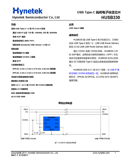
USB Type-C 线缆电子标签芯片Hynetek Semiconductor Co, LtdHUSB330Copyright© 2017, Hynetek Semiconductor Co., Ltd. 1Rev1.1, 5/12/2017功能支持USB Type-C 1.2 和 PD 2.0/3.0 标准通过USB-IF 认证. TID 号: 1000060, XID 号: 0005396 支持SOP’ 通讯集成收发单元 (BMC PHY)同时支持structured VDM version 1.0 和 2.0 高集成度集成两端的Ra 电阻 集成两端的VCONN 二极管 集成 MTP 小封装和易加工:DFN-8L 2 mm x 3 mm x 0.75 mm, 0.50 mm 管间距 DFN-6L 2 mm x 2 mm x 0.75 mm, 0.65 mm 管间距 可选多次烧写或者单次烧写 兼容第三方烧写工具支持 3.0 V ~ 5.5 V 的VCON1 和VCON2引脚供电 定制化CC 引脚烧写 BMC 信号斜率控制减少EMI ±5 kV ESD HBM应用USB Type-C 线缆通用描述HUSB330是USB Type-C 电子标签芯片。
它同时支持USB Type-C 规范1.2,USB USB Power Delivery 规范 2.0 和USB USB Power Delivery 规范 3.0.通过VCON1或者VCON2供电,HUSB330工作在SOP’模式. 自带的多次烧写存储单元(MTP )可支持多次反复烧写或者单次烧写。
HUSB330也可以支持通过CC 引脚实现Type-C 成品头或者成品线缆系统烧写。
HUSB330支持3.0 V 到 5.5 V 范围,与USB-IF 最新支持的VCONN 供电规范一致。
HUSB330有两种封装形式:DFN-8L 和DFN-6L. 它工作在-40°C 到+85°C 温度范围。
芯片电路设计文档:TI OPA855IDSGEVM 3.1 EVM 设计方案、布局和物料清单(BOM
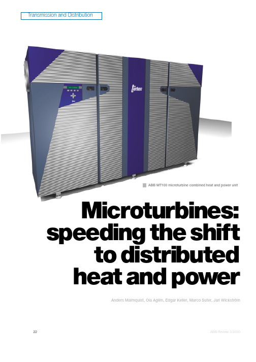
Transmission and DistributionAnders Malmquist, Ola Aglén, Edgar Keller, Marco Suter, Jari WickströmMicroturbines:speeding the shiftto distributed heat and power1ABB MT100 microturbine combined heat and power units part of its business strategy, ABB Distributed Power Generation in 1998 set up a 50/50 joint venture with Volvo Aero Corporation to develop a new generation of microturbines. Thepartnership draws on Volvo’s experience with gas-turbine-driven hybrid electric vehicles as well as ABB’s experience in high-frequency power generation and conversion [1, 2].The first product to come out of this new company, called Turbec AB, is the ABB MT100 Microturbine Combined Heat and Power unit . Run on natural gas, the ABB MT100 generates 100 kW of electricity and 167 kW of thermal energy.At the heart of the ABB MT100 is a small gas turbine, mounted together with a compressor on a single shaft and integrated with a new high-speed generator, the HISEM 110/70.A ‘hot’ new product with a string of benefitsStill a relatively new technology,microturbines have the potential togrows and commercialization drives costs downwards. Features likely to speed up this development include:I Compliance with the latest emissions standardsI Compact and lightweight, passes through a standard door I Low noise levelI Minimal maintenanceI Remote control for unsupervised operationmanufacture and simple design I Fuel flexibility I High efficiencyDesigned for a new era of distributed power generationThe ABB MT100 microturbine is acombined heat and power (CHP) unit, ie it produces electricity and thermalenergy. It is mounted in a small cabinet and runs on natural gas. A compres-21Fewer large power plants and overhead power lines, more efficient use of natural resources,and cheaper electricity – this scenario is within reach thanks to a brand new concept for distributed power generation. Key to its success is the microturbine – a small, highly efficient turbine that can be run on natural gas or biogas. Able to generate even more heat than electricity, the microturbine is eminently well suited as a power source for facilities ranging from hospitals and hotels to shopping malls and factories. With the help of telecommunications systems, such power plants can be linked together to create network solutions that will revolutionize how power is generated and delivered in the future.ATransmission and Distributionsor may be necessary, depending on the natural gas pressure. The ABB MT100 is designed for indoor installation and takes air from an outside intake. Its main parts are:I Gas turbine engine and recuperator I Electrical generatorI Electrical systemI Exhaust-gas heat-exchangerI Supervision and control systemThe technical data of the CHP unit aregiven in Table 1.Design and operationIn the microturbine, a turbine wheeldrives a compressor wheel mounted onthe same shaft . The compressor feedsprocess air into the combustion chamber,where fuel is added and continuouscombustion takes place.The hot gas stream is expanded in theturbine, causing a large part of the thermalenergy to be converted into mechanicalenergy, which drives the compressor andthe load. In conventional power plantsthe load is either a two-pole or four-polegenerator, driven via a gearbox. Thegenerator speed is fixed, since it is syn-chronized with the frequency of anelectric network. In the ABB MT100microturbine the high-speed generator iscoupled directly to the turbine shaft anda static frequency converter adjusts thespeed electronically.The remaining thermal energy can bedissipated through the stack, but such agas turbine will suffer from poor efficiencyunless several compressor and turbinestages are added. The ABB MT100 over-comes this problem with a recuperator,which recovers the exhaust heat and usesit to preheat the compressed air before itenters the combustion chamber. Less fuelis therefore required to reach the desiredoperating temperature. Another heat-exchanger, after the recuperator, heats thewater in the external circuit.Gas turbine emissions are very low asthe continuous combustion can be care-fully controlled. The external combustionchamber can also be optimized for lowemissions.Gas turbines often feature what is3guide vanes control how the gas flows towards the turbine and compressor,allowing the operating point of the gas turbine to be controlled. Here too, the designers of the ABB MT100 took a different approach. The electric power generation system with the frequency which allows the power to be controlled by adjusting the turbine speed within a wide range. A simpler turbine concept can therefore be chosen, keeping product costs down. Details of the microturbine and a description of gas turbines in general can be found in [3] and [4], respectively .Housing Compressor RecuperatorCombustion chamber TurbineThe electrical generator andThe engine parts and the shaft are located in the same housing.Compressor:In the ABB MT100, aradial centrifugal compressor is used to compress the ambient air. The pressure ratio is about 4.5:1. The compressor isP e =100 kW658Following ABB’s transformation into a knowledge company, ABB Distributed Power Generation wasestablished as a new business unit to serve the changing power market.Instead of selling hardware, the business of the new unit is to sell energy service solutions to customers in need of power, heating and/or cooling.Selling service rather than equipment calls for acombination of technology and financing. ABB Distributed Power Generation installs, on the customer’s premises, a compact generating unit which it owns, operates remotely and maintains as necessary. Customers pay only for the output, freeing up capital which they can invest in their core business.How else does the customer benefit? By gaining a cost advantage over competitors in the marketplace. We are able to offer locally generated energy services at a lower price than with conventional solutions by avoiding thetransmission and distribution costs, with heat provided as a useful by-product.The second, and perhaps even more important,advantage to the customer lies in the power quality andsafety areas. Although no longer so common, poweroutages still do occur occasionally. And each one poses a severe risk to the customer’s processes, and by extension to his revenues. Installing a microturbine unit, combined with connection to the public grid, makes power outages extremely unlikely, thereby securing reliable operation for processes and computer systems, as well as an uninterrupted revenue stream.Summing up: ABB is able to offer an energy service which costs less and offers more than competing solutions,and which requires no upfront investment by the customer.Typical application areas are office buildings, shoppingcenters, greenhouses, regions with a weak grid connection,hospitals, leisure centers, etc.Transmission and distribution systems in some areas tend to be overloaded, and environmental or otherlegislation may make expanding them a long and tedious process. Using state of the art information technology, such as the Internet, a large number of microturbines and other distributed power generation resources can be linked and controlled by an operator who is in charge of what is, in effect, a large ’virtual’ utility.Microturbines: the ‘upside’ of downsizing3ABB MT100: thermodynamic processes1Generator, 2Inlet air, 3Combustion chamber, 4Air to recuperator, 5Compressor, 6Turbine, 7Recuperator, 8Exhaust gases, 9Exhaust-gas heat-exchanger, 10Exhaust-gas outlet, 11Hot-water outlet, 12Water inletTransmission and Distributionmounted on the same shaft as the turbine and the electrical generator.Recuperator:The recuperator is a gas-to-air heat-exchanger attached to the microturbine. It increases the efficiency of the gas turbine by transferring the heat from the hot exhaust gases to the compressed air fed to the combustion chamber.Combustion chamber:The preheated compressed air is mixed with the natural gas, and an electrical igniter in the combustion chamber ignites the mixture. The combustion chamber is of the lean pre-mix emission type, guaranteeing low emissions of NO x, CO and unburned hydrocarbons in the exhaust gases.Turbine:The radial turbine drives the compressor and the generator at a nominal speed of 70,000 rev/min. On leaving the combustion chamber the combustion gases have a temperature of approximately 950°C and are at a pressure of about 4.5 bar. As the gases expand through the turbine the pressure decreases to close to atmospheric and the heat drops to approximately 650°C.Exhaust-gas heat-exchanger:The exhaust-gas heat-exchanger is of the gas/water counter-current flow type. It transfers the thermal energy contained in the exhaust gases, which enter the heat-exchanger at a temperature of approx-imately 270°C, to the hot-water system. The outlet water temperature depends on the incoming water conditions, ie itsgases leaving the heat-exchanger passthrough an exhaust pipe to the stack.Supervision and control systemThe ABB MT100 is controlled andsupervised automatically by the PowerModule Controller (PMC), so that innormal use the CHP unit can be leftunsupervised. If a critical fault shouldoccur, the PMC initiates either a normalstop or an emergency shutdown,whichever is necessary. A fault code isrecorded by the PMC and shown on thedisplay on the control panel.The gas turbine and the electric powergeneration system are operated andcontrolled automatically by the PMC.Values from a number of sensors areneeded by the PMC for this:I Heat demandI Electric power demandI Gas pressureI Oil temperatureI VibrationsI SpeedHigh-speed electric powergeneration systemSmall gas turbines benefit in particularwhen the gearbox that reduces theturbine shaft speed to the speed ofconventional electrical machines iscompact and reliable machine. With sucha system, the shaft speed is normallyabove 30,000 rev/min and may exceed100,000 rev/min.High-energy permanent magnets andhigh yield-strength materials are state ofthe art, and have proved very suitable forhigh-speed electrical machines. Forexample, the use of neodymium-iron-boron (NdBFe) magnets reduces thegenerator rotor losses.A prerequisite for direct mechanicalcoupling is highly efficient frequencyconversion. Insulated gate bipolartransistors (IGBTs) not only provide thisgood efficiency, they can also beswitched at an appropriately highfrequency. Machines based on thesedevices are tailor-made for certain high-speed applications.An advantage of the high-speedgenerator is that the size of the machinedecreases almost in direct proportion tothe increase in speed, leading to a verysmall unit that can be integrated with thegas turbine.Electrical systemBefore the generated power can be sentto the grid, it has to be converted to thegrid frequency . The AC of thegenerator is first rectified to DC and then44Schematic of the electric power generation1Generator, 2Rectifier/start-up converter, 3DC bus, 4Converter, 5Line filter,6EMC filter, 7Main circuit-breakerconverted to three-phase AC. Aninductor stabilizes the AC output, whilean EMC filter protects the grid againstgenerated interference. The electricalsystem can also be used as a powersupply for starting the gas turbine.High-speed generatorThe electric power is generated by anHISEM 110/70 high-speed permanentmagnet synchronous generator, which isintegrated with the microturbine .The rotor is suspended by one bearingon each side of the permanent magnetrotor; there are no additional bearings onthe turbine shaft. The output frequencyof the generator is high, being up to2.3 kHz. The generator – acting as anelectric starter for the gas turbine – alsostarts the CHP unit.Generator design:The generatordesign is derived from the HSG100generator [5], developed for use in hybridvehicles. Experience gained from micro-turbine applications and the need to takeaccount of some new requirements, haveled to several major improvements,especially with regard to reliability andproduction costs. Also of benefit was ABBMotors’ experience with high-volume pro-duction, which could also be incorporatedin the design.The generator stator can be seenin . Its core consists of thin laminationsof low-loss electrical steel and thewinding is made with litz wire to achievegood high-frequency characteristics. Thefour-pole arrangement contributes toshort end-windings, making it possible to655HISEM 110/70 generator and turbine being set up for testing6Cutaway view of the HISEM 110/70 generatorTransmission and Distributionkeep the distance between the bearings short.Water-cooling is used to keep the temperature low in the winding. This feature, plus the vacuum pressure impregnation and extra insulation,ensures a long lifetime for the winding. The rotor consists of a magnetic steel body with surface-mounted permanent magnets. A carbon-fiberbandage holds the magnets firmly in place, even at 70,000 rev/min. As theoperating conditions differ considerably from those for conventional machines,ordinary analytical programs are not enough for the electrical machine design.One hugely influential factor is the high fundamental frequency of 2.3 kHz at 70,000 rev/min, which makes the parameters of conventional design programs – parameters empirically determined over years of conventional machine design – invalid. A design strategy was therefore chosen that combines analytical calculations with finite element analysis.The rotor radius is selected according to mechanical design criteria, and is a trade-off between an optimum bendingstiffness and the largest magnet thickness that can be retained by a reasonably thin bandage. Using the rotor radius as a basis,the stator core radius and the axial length are determined in an iterative process.The discrete nature of the stator winding,with its very limited number of turns, is a key constraint.It is important to make sure that the rotor never reaches a temperature that would de-magnetize the magnet. This is ensured both by reducing the rotor losses and providing efficient cooling in the air-gap. Two factors, air friction andasynchronous mmf waves in the air-gap,are the main cause of temperature rise in the rotor. The latter is mainly due to harmonics in the stator current. Because the high speed causes high friction losses and the carbon-fiber bandage acts as a thermal insulator, the rotor is more sensitive to current harmonics than the rotor in a conventional machine. A current harmonics limit was therefore defined which is based on the acceptable rotor losses.Frequency converterThe factors that provided the biggest challenge to the designers of thefrequency converter were the high input frequency of 2300 Hz and the product cost target. The microturbine converter is derived from the ACS 600 converter platform, while the grid-side functions were available in the ACA 635 Inverter Supply Module. However, extensive application programming was needed to implement the interface and control functions required for the microturbine application.The generator input stage, including the start-up converter, is based on hardware from the ACS 600, but a new control board had to be developed to regulate the speed of the turbine and control starting. In the start mode, the rectifier is used as an inverter toaccelerate the turbine to 30,000 rev/min,the speed from which the turbine starts to produce net power for furtheracceleration to the operating range of 50,000 to 70,000 rev/min. The start-up converter acts as a rectifier and supplies electric power to the DC bus, from where77Generator rotor 8Frequency converternetwork.The ACS 600 series converters are designed to operate in an industrial environment, while in the microturbine application they have to meet the requirements for residential area installations. Although distributed power generation applications are still a ‘gray zone’ with respect to grid regulations, it was decided to adapt the converter to comply with EN50081.While the source of the functional hardware is the ACS 600 series, the mechanical installation has been tailored for the microturbine application . An important feature here is the use of water-cooling.System analysisIn a typical microturbine application it is likely that the grid topology will not be known, so that controlling the system stability can be a challenging task. In cases where distributed power the risk of grid instability may be verypronounced. Since there is more thanone controller, even internal oscillationsmay appear all of a sudden, as tests onthe pre-prototype CHP unit [7] at ABBCorporate Research in Dättwil,Switzerland, showed.To avoid this kind of instability,different simulation models have beenestablished. These were derived fromprevious work on the hybrid bus [6], fromthe topology of the CHP system and frommeasurements. Some of the models aretime-domain-based and are used tounderstand and study the entire system aswell as the different interfaces betweenthe sub-systems. Possible problems areshown in . It goes without saying thatABB MT100 must be able to handle all ofthese without damage being caused toitself or to equipment outside of themicroturbine system.Other models are frequency-domain-based [8], allowing a more straightforwardanalysis and identifying possible locationsof instabilities in the system, mainlytowards the grid. This work is based onexperience with railway systems, where ashutdown due to such instabilitiesoccurred some years ago [9]. Such modelsare defined by generating a frequencyspectrum of every component involved inthe system, eg the inverter or a specialtype of grid topology. By combiningthese spectra and analyzing them,instabilities in the system can be rapidlylocated. This analysis results in thecomponents – mainly the controllers –being designed such that stableinteroperability of the entire system andits neighbors is ensured.Maintenance conceptA key property of the ABB MT100 CHPunit is that it requires only very littlemaintenance. Preventive, ie scheduled,maintenance is divided into inspectionsand overhauls (see Table 2). Due to the989Grid interface problems having an impact on DPG unitsTransmission and Distributionmaintenance can be limited to the work shown in Table 3.OutlookThe potential market for distributed power resources is a large andmarket, a standard unit is required that is affordable, reliable and environmentally benign. The ABB MT100 microturbine meets these requirements withsubsystems that have been derived from vanguard ABB technologies. Combinedwith IT functionality that provides safe,unsupervised operation, the ABB MT100microturbine points the way to a whole new era in distributed power generation.References[1] P. Chudi , A. Malmquist : A hybrid drive for the car of the future. ABB Review 9/93, 3-12.[2] G. Lagerström ,A. Malmquist : Advanced hybrid propulsion system for Volvo ECT. Volvo Technology Report no 2, 1995. [3] D10365 v1 - Technical Information, Turbec AB 2000.[4] D.K. Mukherjee : State-of-the-art gas turbines – a brief update. ABB Review 2/97, 4-14.[5] P. Chudi ,A. Malmquist : Development of a small gas turbine driven high speed permanent magnet generator.Licentiate thesis, The Royal Institute of Technology. KTH 1989.[6] A. Malmquist : Analysis of a gas turbine driven hybrid drive train for heavy vehicles. Ph.D. thesis, The Royal Institute of Technology. KTH 1999.[7] M. Suter : Do it yourself. Akzent, ABB Switzerland, no 2/2000.[8] E. Moellerstedt ,B. Bernhardsson : Out of control because of harmonics: an analysis of the harmonics response of an inverter locomotive. IEEE Control Systems Magazine, August 2000.[9] M. Meyer ,J. Schöning : Netzstabilität in grossen Bahnnetzen, Eisenbahn-Revue, July-August 1999.。
主板CPU供电芯片(驱动部分)
DS9605B-01C November 2005All brandname or trademark belong to their owner respectivelyGeneral DescriptionThe RT9605B is a high frequency, triple-channel synchronous-rectified buck MOSFET driver specifically designed to drive six power N-Channel MOSFETs. The part is promoted to pair with RichTek's multiphase buck PWM controller family for high-density power supply implementation. The output drivers of RT9605B can efficiently switch power MOSFETs at frequency 300kHz typically. Operating in higher frequency should consider the thermal dissipation carefully. Each driver of RT9605B is capable to drive a 3nF load in 30/40ns rising/falling time with little propagation delay from input transition to the gate of the power MOSFET . The device implements bootstrapping on the upper gate with only an external capacitor and a diode required. This reduces circuit complexity and allows the use of higher performance, cost effective N-Channel MOSFETs. All drivers incorporate adaptive shoot-through protection to prevent upper and lower MOSFETs from conducting simultaneously and shorting the input supply. The RT9605B also detects the fault condition during initial start-up prior to the multi-phase PWM controller takes control. As a result, the input supply will latch into the shutdown state. The RT9605B comes to a small footprint package with QFN-24L 4x4 package.FeatureszDrive Six N-Channel MOSFETs for 3-Phase Buck PWM Controlz Adaptive Shoot-Through Protection z Support High Switching Frequency z Fast Output Rise/Fall Time z Propagation Delay 40nsz Tri-State Input for Bridge Shutdown z Upper MOSFET Direct Short Protection z Small 24-Lead QFN PackagezRoHS Compliant and 100% Lead (Pb)-FreeApplicationsz CPU Core Voltage Supplies on Motherboard z High Frequency Low Profile DC-DC Converters zHigh Current Low Voltage DC-DC ConvertersTriple-Channel Synchronous-RectifiedBuck MOSFET DriverOrdering InformationMarking InformationFor marking information, contact our sales representative directly or through a RichTek distributor located in your area, otherwise visit our website for detail.Pin Configurations(TOP VIEW)QFN-24L 4x4Note :RichTek Pb-free products are :−RoHS compliant and compatible with the current require- ments of IPC/JEDEC J-STD-020.−Suitable for use in SnPb or Pb-free soldering processes.−100% matte tin (Sn) plating.P : Pb Free with Commercial StandardUGATE1GND GNDLGATE3PVCC3BOOT2UGATE2GNDPWM2PWM1NC BOOT1P W M 3V D DB O O T 3U G A T E 3P H A S E 3G N DP H A S E 1L G A T E 1P V C C 1P V C C 2L G A T E 2P H A S E 2Typical Application Circuit Functional Pin DescriptionUGATE1 (Pin 1), UGATE2 (Pin 17), UGATE3 (Pin 10) Upper Gate Drive Output. Should be connected to the upper MOSFET gate.BOOT1 (Pin 2), BOOT2 (Pin 16), BOOT3 (Pin 9) Floating bootstrap supply pin for the upper gate drive. Connect the bootstrap capacitor between this pin and the PHASE pin. The bootstrap capacitor provides the charge to turn on the upper MOSFET.NC (Pin 3)No connected.PWM1 (Pin 4), PWM2 (Pin 5), PWM3 (Pin 7)PWM input control signal. Connect this pin to the PWM output of the controller. If the PWM signal enters and remains within the shutdown window, are both UGATE and LGATE are drived low, disabling the output MOSFET s.GND (Pin 6, 12, 13, 18 )Chip power ground.VDD (Pin 8)Supply Input. Connect to +5V stand-by power. Place a bypass capacitor between this pin and GND.PHASE1 (Pin 24), PHASE2 (Pin 19), PHASE3 (Pin 11) Upper driver return. Should be connected to the common node of upper and lower MOSFETs. The PHASE voltage is monitored for adaptive shoot-through protection.LGATE1 (Pin 23), LGATE2 (Pin 20), LGATE3 (Pin 14) Lower Gate Drive Output. Should be connected to the lower MOSFET gate.PVCC1 (Pin 22), PVCC2 (Pin 21), PVCC3 (Pin 15) Supply Input. Connect to +12V supply. Place a bypass capacitor between this pin and PGND.Exposed PadExposed pad should be soldered to PCB board and connected to GND.All brandname or trademark belong to their owner respectivelyDS9605B-01C November 2005All brandname or trademark belong to their owner respectivelyFunction Block DiagramTiming DiagramPWMUGATE LGATEAll brandname or trademark belong to their owner respectivelyAbsolute Maximum Ratings (Note 1)z Supply Voltage, P VCC -----------------------------------------------------------------------------------15V z Supply Voltage, V DD -------------------------------------------------------------------------------------7VzPHASE to GNDDC------------------------------------------------------------------------------------------------------------−5V to 15V < 200ns -----------------------------------------------------------------------------------------------------−10V to 30Vz BOOT to PHASE -----------------------------------------------------------------------------------------15VzBOOT to GNDDC------------------------------------------------------------------------------------------------------------−0.3V to V CC +15V < 200ns -----------------------------------------------------------------------------------------------------−0.3V to 42V z PHASE to GND -------------------------------------------------------------------------------------------−4V to 15Vz PWM Input Voltage --------------------------------------------------------------------------------------GND - 0.3V to 7Vz UGATE ------------------------------------------------------------------------------------------------------V PHASE - 0.3V to V BOOT + 0.3V z LGATE ------------------------------------------------------------------------------------------------------GND - 0.3V to V PVCC + 0.3V zPackage Thermal Resistance (Note 4)QFN-24L 4x4, θJA ----------------------------------------------------------------------------------------67°C /W z Lead Temperature (Soldering, 10 sec.)--------------------------------------------------------------260°Cz Storage T emperature Range ---------------------------------------------------------------------------−40°C to 150°C zESD Susceptibility (Note 2)HBM (Human Body Mode)-----------------------------------------------------------------------------1kV MM (Machine Mode)-------------------------------------------------------------------------------------100VElectrical CharacteristicsRecommended Operating Conditions (Note 3)z Supply Voltage, V DD -------------------------------------------------------------------------------------12V ±10%z Ambient Temperature Range ---------------------------------------------------------------------------0°C to 70°C zJunction T emperature Range ---------------------------------------------------------------------------0°C to 125°C(Recommended Operating Conditions, T A = 25°C unless otherwise specified)To be continuedNote 1. Stresses listed as the above “Absolute Maximum Ratings”may cause permanent damage to the device. These are for stress ratings. Functional operation of the device at these or any other conditions beyond those indicated in the operational sections of the specifications is not implied. Exposure to absolute maximum rating conditions for extended periods may remain possibility to affect device reliability.Note 2. Devices are ESD sensitive. Handling precaution recommended.Note 3. The device is not guaranteed to function outside its operating conditions.Note 4. θJA is measured in the natural convection at T A = 25°C on a low effective thermal conductivity test board of JEDEC 51-3 thermal measurement standard.All brandname or trademark belong to their owner respectivelyDS9605B-01C November Application InformationThe RT9605B is designed to drive three sets of both high side and low side N-Channel MOSFET through externally input PWM control signal. It has power-on protection function which held UGATE and LGATE low before PV CC rising across the threshold voltage. After the initialization, the PWM signal takes the control. The rising PWM signal first forces the LGATE turns low then UGATE is allowed to go high just after a non-overlapping time to avoid shoot-through. The falling of PWM signal first forces UGATE to go low. When UGATE and PHASE reach a predetermined low level, LGATE is allowed to turn high. The non-overlapping function is also presented between UGATE and LGATE signal transient.The PWM signal is acted as "High" if above the rising threshold and acted as "Low" if below the falling threshold. Any signal level remaining within the shutdown window is considered as "tri-state", the output drivers are disabled and both MOSFET gates are pulled and held low. If the PWM signal floating, the pin will be kept at 2.1V by the internal divider and provide the PWM controller with a recognizable level.The RT9605B typically operates at frequency of 200kHz to 300kHz. It shall be noted that to place a 1N4148 or schottky diode between the PVCC and BOOT pin asshown in the typical application circuit.Driving Power MOSFETsThe DC input impedance of the power MOSFET is extremely high. When V gs at 12V, the gate draws the current only few nano-amperes. Thus once the gate has been driven up to "ON" level, the current could be negligible.However, the capacitance at the gate to source terminal should be considered. It requires relatively large current to source and sink the gate rapidly. It also needs to switch drain current on and off with high speed. The required gate drive currents are calculated as follows.In Figure 1, the current I g1 and I g2 are required to move the gate up to 12V. The operation consists of charging C gd and C gs. C gs1 and C gs2are the capacitances from gate to source of the high side and the low side power MOSFETs, respectively. In general data sheets, the C gs is referred as "C iss" which is the input capacitance. C gd1 and C gd2are the capacitances from gate to drain of the high side and the low side power MOSFETs, respectively and referred to the data sheets as "C rss" the reverse transfer capacitance. For example, t r1and t r2are the rising time of the high side and the low side power MOSFETs respectively, the required current I gs1and I gs2,are showed below:Figure 1. Equivalent Circuit and Associated WaveformsV OUT VGND VVr2gs2g2gs2gs2r1gs1g1gs1gs1t12CdtdVCIt12CdtdVCI×==×==(1)(2)All brandname or trademark belong to their owner respectivelyDS9605B-01C November 2005All brandname or trademark belong to their owner respectivelyBefore driving the gate of the high side MOSFET up to 12V (or 5V), the low side MOSFET has to be off; and the high side MOSFET is turned off before the low side is turned on. From Figure 1, the body diode "D 2" had been turned on before high side MOSFETs turned on.It is helpful to calculate these currents in a typical case.Assume a synchronous rectified buck converter, input voltage V IN = 12V, V g1 = V g2 = 12V. The high side MOSFET is PHB83N03LT whose C iss = 1660pF,C rss = 380pF, and t r = 14ns. The low side MOSFET is PHB95N03LT whose C iss = 2200pF, C rss = 500pF and t r = 30ns, from the equation (1) and (2) we can obtain from equation. (3) and (4)the total current required from the gate driving source isBy a similar calculation, we can also get the sink current required from the turned off MOSFET .Layout ConsiderationFigure 2 shows the schematic circuit of a two-phase synchronous buck converter to implement the either phase of RT9605B. The converter operates at V IN 12V.When layout the PC board, it should be very careful. Thepower-circuit section is the most critical one. If not configured properly, it will generate a large amount of EMI.The junction of Q1, Q2, L2 should be very close.Next, the trace from UGATE, and LGATE to the gates of MOSFET should also be short to decrease the noise of the driver output signals. The bypass capacitor C4 should be connected to GND directly. Furthermore, the bootstrap capacitors (C B ) should always be placed as close to the pins of the IC as possible. The trace from PHASE to the common node of the two MOSFETs should be kept wide since it usually carries large current.Select the Bootstrap CapacitorFigure 3 shows part of the bootstrap circuit of RT9605B.The V CB (the voltage difference between BOOT and PHASE pins provides a voltage to the gate of the high side power MOSFET. This supply needs to be ensured that the MOSFET can be driven. For this, the capacitance C B has to be selected properly. It is determined by following constraints.Figure 2. Sync. Buck Converter CircuitFigure 3. Part of Bootstrap Circuit of RT9605Br2IN gd2gd2gd2t 12VV C dt dV C I +==(4)(3)r1gd1g1gd1t 12VC dt dV C I ==(5)(6)(7)(8)(A)1.280.4)(0.88I I I (A) 1.7450.326)(1.428I I I gd2gs2g2gd1gs1g1=+=+==+=+=(9)(10)Before the low side MOSFET is turned on, the C gd2 have been charged to V IN . Thus, as C gd2 reverses its polarity and g 2 is charged up to 12V, the required current isV CB +-(A)0.410301210500I (A)0.32610141210380I 912-912gd2gd1=×××==×××=−−−(A)0.88103012102200I (A)1.428101412101660I 912-912gs2gs1=×××==×××=−−−12VV VAll brandname or trademark belong to their owner respectivelyOver-Voltage Protection Function at Power-OnAn unique feature of the RT9605B is the addition of over-voltage protection in the event of upper MOSFET direct shorted before power-on. The RT9605B detects the fault condition during initial start-up, the internal power-on OVP sense circuitry will rapidly drive the low side MOSFET on before the multi-phase PWM controller takes control.Figure 6 shows the measured waveforms with the high side MOSFET directly shorted to 12V.Please note that the +12V trigger point to RT9605B is at 3V, and the clamped level on PHASE pin is at about 2.4V.Obviously since the PHASE pin voltage increases during initial start-up, the V CORE increases correspondingly, but it would quickly drop-off following the voltage in LGATE and +12V.In practice, a low value capacitor C B will lead the over-charging that could damage the IC. Therefore to minimize the risk of overcharging and reducing the ripple on V CB ,the bootstrap capacitor should not be smaller than 0.1μF,and the larger the better. In general design, using 1μF can provide better performance. At least one low-ESR capacitor should be used to provide good local de-coupling. Here,to adopt either a ceramic or tantalum capacitor is suitable.Power DissipationFor not exceeding the maximum allowable power dissipation to drive the IC beyond the maximum recommended operating junction temperature of 125°C,it is necessary to calculate power dissipation appro-priately. This dissipation is a function of switching frequency and total gate charge of the selected MOSFET .Figure 4 shows the power dissipation test circuit. C L and C U are the UGATE and LGATE load capacitors,respectively. The bootstrap capacitor value is 1μF.Figure 5 shows the power dissipation of the RT9605B as a function of frequency and load capacitance. The value of the C U and C L are the same and the frequency is varied from 100kHz to 1MHz.The operating junction temperature can be calculated from the power dissipation curves (Figure 5). Assume VDD = 12V, operating frequency is 200kHz and the C U =C L =1nF which emulate the input capacitances of the high side and low side power MOSFETs. From Figure 5,the power dissipation is 100mW. For RT9605B, the package thermal resistance θJA is 67°C/W, the operating junction temperature is calculated as:T J = (67°C/W x 100mW) + 25°C = 31.7°C (11)where the ambient temperature is 25°C.Figure 4. Test Circuit (One Phase is Shown)The method to improve the thermal transfer is to increase the PC board copper area around the RT9605B firstly.Then, adding a ground pad under IC to transfer the heat to the peripheral of the board.Figure 6. Waveforms at High Side MOSFET Shorted +12VPHASE XLGATE XV COREFigure 5. Power Dissipation vs. Frequency Power Dissipation vs. Frequency0100200300400500600700800900100002004006008001000Frequency (kHz)P o w e r D i s s i p a t i o n (m W )20All brandname or trademark belong to their owner respectivelyDS9605B-01C November RICHTEK TECHNOLOGY CORP. Headquarter5F, No. 20, Taiyuen Street, Chupei City Hsinchu, Taiwan, R.O.C.Tel: (8863)5526789 Fax: (8863)5526611RICHTEK TECHNOLOGY CORP.Taipei Office (Marketing)8F-1, No. 137, Lane 235, Paochiao Road, Hsintien City Taipei County, Taiwan, R.O.C.Tel: (8862)89191466 Fax: (8862)89191465Email: marketing@V-Type 24L QFN 4x4 Package。