RLT6505G中文资料
65050资料
FEATURES APPLICATIONSDESCRIPTIONTPS65050,TPS65051,TPS65052TPS65054,TPS65056SLVS710–JANUARY2007 6-CHANNEL POWER MGMT IC WITH TWO STEP-DOWN CONVERTERSAND4LOW-INPUT VOLTAGE LDOs•Cell Phones,Smart-Phones•Up To95%Efficiency•WLAN•Output Current for DC/DC Converters:•PDAs,Pocket PCs–TPS65050:2x0.6A•OMAP™and Low-Power TMS320™DSP –TPS65051:DCDC1=1A;DCDC2=0.6ASupply–TPS65052:DCDC1=1A;DCDC2=0.6A•Samsung S3C24xx application processor –TPS65054:2x0.6A Supply–TPS65056:DCDC1=1A;DCDC2=0.6A•Portable Media Players•Output Voltages for DC/DC Converters–TPS65050:Externally AdjustableThe TPS6505x are integrated Power Management –TPS65051:Externally AdjustableICs for applications powered by one Li-Ion or –TPS65052:DCDC1=Fixed at3.3V;Li-Polymer cell,which require multiple power rails.DCDC2=1V/1.3V for SamsungThe TPS6505x provides two efficient, 2.25-MHz Application Processors step-down converters targeted at providing the core–TPS65054:DCDC1=Externally Adjustable;voltage and I/O voltage in a processor based DCDC2=1.3V/1.05V for OMAP™1710system.Both step-down converters enter a lowpower mode at light load for maximum efficiency Processoracross the widest possible range of load currents.–TPS65056:DCDC1=Fixed at3.3V;DCDC2=1V/1.3V for Samsung For low noise applications,the devices can be forced Application Processors into fixed frequency PWM mode by pulling theMODE pin high.In the shutdown mode,the current •V I Range for DC/DC Convertersconsumption is reduced to less than1µA.The From2.5V to6Vdevices allow the use of small inductors and • 2.25-MHz Fixed Frequency Operation capacitors to achieve a small solution size.•Power Save Mode at Light Load Current TPS6505x provides an output current of up to1A oneach DC/DC converter.The TPS6505x also integrate •180°Out-of-Phase Operationtwo400-mA LDO and two200-mA LDO voltage •Output Voltage Accuracy in PWM mode±1%regulators,which can be turned on/off using separate•Low Ripple PFM Mode enable pins on each LDO.Each LDO operates withan input voltage range between 1.5V and 6.5V •Total Typical32-µA Quiescent Current forallowing them to be supplied from one of the Both DC/DC Convertersstep-down converters or directly from the main •100%Duty Cycle for Lowest Dropout battery.•Two General-Purpose400-mA,High PSRRFour digital input pins are used to set the output LDOsvoltage of the LDOs from a set of16different •Two General-Purpose200-mA,High PSRR combinations for LDO1to LDO4on TPS65050and LDOs TPS65052.In TPS65051,TPS65054and TPS65056,the LDO voltages are adjustable using external •V I range for LDOs from1.5V to6.5Vresistor dividers.•Digital Voltage Selection for the LDOsThe TPS6505x come in a small32-pin leadless •Available in a4mm x4mm32-Pin QFNpackage(4mm x4mm QFN)with a0.4mm pitch.PackagePlease be aware that an important notice concerning availability,standard warranty,and use in critical applications of TexasInstruments semiconductor products and disclaimers thereto appears at the end of this data sheet.OMAP,TMS320,PowerPAD are trademarks of Texas Instruments.UNLESS OTHERWISE NOTED this document contains Copyright©2007,Texas Instruments Incorporated PRODUCTION DATA information current as of publication date.Products conform to specifications per the terms of TexasInstruments standard warranty.Production processing does notnecessarily include testing of all parameters.ABSOLUTE MAXIMUM RATINGSDISSIPATION RATINGSRECOMMENDED OPERATING CONDITIONSTPS65050,TPS65051,TPS65052TPS65054,TPS65056SLVS710–JANUARY 2007These devices have limited built-in ESD protection.The leads should be shorted together or the device placed in conductive foam during storage or handling to prevent electrostatic damage to the MOS gates.ORDERING INFORMATIONPART OUTPUT CURRENT QFN (1)PACKAGE T AOPTIONNUMBER for DC/DC CONVERTERSPACKAGE (2)MARKING LDO voltages according to Table 1TPS650502x 600mA 65050DC/DC converters externally adjustable LDO voltages externally adjustable DCDC1=1A TPS6505165051DC/DC converters externally adjustable DCDC2=600mA LDO voltages according to Table 1DCDC1=1A TPS6505265052DCDC1=3.3V;DCDC2=1V /1.3V DCDC2=600mA -40°C to 85°CRSMLDO voltages externally adjustable TPS65054DCDC1=externally adjustable 2x 600mA 65054DCDC2=1.3V /1.05V LDO voltages externally adjustableDCDC1=1A TPS65056DCDC1=3.3V 65056DCDC2=600mADCDC2=1.0V /1.3V(1)The RSM package is available in tape and reel.Add the R suffix (TPS65050RSMR)to order quantities per reel.Add the T suffix (TPS65050RSMT)to order quantities of 250parts per reel.(2)For the most current package and ordering information,see the Package Option Addendum at the end of this document,or see the TI Web site at .over operating free-air temperature range (unless otherwise noted)(1)UNITSInput voltage range on all pins except AGND,PGND,and EN_LDO1pins with -0.3V to 7V respect to AGNDV IInput voltage range on EN_LDO1pins with respect to AGND-0.3V to V CC +0.5VCurrent at VINDCDC1/2,L1,PGND1,L2,PGND21800mA I ICurrent at all other pins1000mAContinuous total power dissipationSee the dissipation rating tableT A Operating free-air temperature –40°C to 85°CT J Maximum junction temperature 125°C T stg Storage temperature range–65°C to 150°C(1)Stresses beyond those listed under "absolute maximum ratings"may cause permanent damage to the device.These are stress ratings only and functional operation of the device at these or any other conditions beyond those indicated under "recommended operating conditions"is not implied.Exposure to absolute-maximum-rated conditions for extended periods may affect device reliability.POWER RATINGDERATING FACTOR POWER RATINGPOWER RATINGPACKAGE R θJA (1)T A ≤25°CABOVE T A =25°CT A =70°CT A =85°CRSM58K/W1.7W17mW/K0.95W0.68W(1)The thermal resistance junction to case of the RSM package is 4K/W measured on a high K boardover operating free-air temperature range (unless otherwise noted)MINNOMMAXUNIT V I Input voltage range for step-down converters,VINDCDC1/2 2.56V Output voltage range for step-down converter,VDCDC10.6VINDCDC1/2V V O Output voltage range for step-down converter,VDCDC20.6VINDCDC1/2V V IInput voltage range for LDOs,VINLDO1,VINLDO2,VINLDO3/41.56.5V2Submit Documentation FeedbackELECTRICAL CHARACTERISTICS TPS65050,TPS65051,TPS65052TPS65054,TPS65056SLVS710–JANUARY2007RECOMMENDED OPERATING CONDITIONS(continued)over operating free-air temperature range(unless otherwise noted)MIN NOM MAX UNITVINLDO1, Output voltage range for LDO1and LDO21VVINLDO2V OOutput voltage range for LDO3and LDO41VINLDO3/4VOutput current at L1(DCDC1)for TPS65051,TPS650521000mAOutput current at L1(DCDC1)for TPS65050,TPS65054600mA I O Output current at L1(DCDC2)600mAOutput current at VLDO1,VLDO2400mAOutput current at VLDO3,VLDO4200mAInductor at L1,L2(1) 1.5 2.2µHOutput capacitor at VDCDC1,VDCDC2(2)1022µF C OOutput capacitor at VLDO1,VLDO2,VLDO3,VLDO4(2) 2.2µFInput capacitor at VCC(2)1µF C I Input capacitor at VINLDO1/2(2) 2.2µFInput capacitor at VINLDO3/4(2) 2.2µF T A Operating ambient temperature range-4085°C T J Operating junction temperature range-40125°C Resistor from battery voltage to V CC used for filtering(3)110Ω(1)See the Application Information section of this data sheet for more details.(2)See the Application Information section of this data sheet for more details.(3)Up to2mA can flow into V CC when both converters are running in PWM,this resistor causes the UVLO threshold to be shiftedaccordingly.V CC =VINDCDC1/2=3.6V,EN=VCC,MODE=GND,L=2.2µH,CO=10µF.TA=-40°C to85°C,typical values are atTA=25°C(unless otherwise noted).PARAMETER TEST CONDITIONS MIN TYP MAX UNIT SUPPLY CURRENTV I Input voltage range at VINDCDC1/2 2.56VOne converter,I O=0mA.PFM mode enabled(Mode=GND)device not2030µAswitching,EN_DCDC1=V I OR EN_DCDC2=V I;EN_LDO1=EN_LDO2=EN_LDO3/4=GNDTwo converters,I O=0mAOperating quiescent current PFM mode enabled(Mode=0)device not3240µAI Q Total current into V CC,VINDCDC1/2,switching,EN_DCDC1=V I AND EN_DCDC2=V I;VINLDO1,VINLDO2,VINLDO3/4EN_LDO1=EN_LDO2=EN_LDO3/4=GNDOne converter,I O=0mA.PFM mode enabled(Mode=GND)device notswitching,EN_DCDC1=V I OR EN_DCDC2=V I;180250µAEN_LDO1=EN_LDO2=EN_LDO3=EN_LDO4=V IOne converter,I O=0mA.Switching with no load(Mode=V I),PWM operation0.85mAEN_DCDC1=V I OR EN_DCDC2=V I;EN_LDO1=EN_LDO2=EN_LDO3/4=GNDI Q Operating quiescent current into V CCTwo converters,I O=0mASwitching with no load(Mode=V I),PWM operation1.25mAEN_DCDC1=V I AND EN_DCDC2=V I;EN_LDO1=EN_LDO2=EN_LDO3/4=GNDEN_DCDC1=EN_DCDC2=GND EN_LDO1=I(SD)Shutdown current912µAEN_LDO2=EN_LDO3=EN_LDO4=GNDUndervoltage lockout threshold forV(UVLO)Voltage at V CC 1.82V DCDC converters and LDOs3Submit Documentation FeedbackTPS65050,TPS65051,TPS65052TPS65054,TPS65056SLVS710–JANUARY 2007ELECTRICAL CHARACTERISTICS (continued)V CC =VINDCDC1/2=3.6V,EN =V CC ,MODE =GND,L =2.2µH,C O =10µF.T A =-40°C to 85°C,typical values are at T A =25°C (unless otherwise noted).PARAMETERTEST CONDITIONSMINTYPMAXUNITEN_DCDC1,EN_DCDC2,DEFDCDC2,DEFLDO1,DEFLDO2,DEFLDO3,DEFLDO4,EN_LDO1,EN_LDO2,EN_LDO3,EN_LDO4MODE/DATA,EN_DCDC1,EN_DCDC2,DEFDCDC2,DEFLDO1,DEFLDO2,DEFLDO3,V IHHigh-level input voltage1.2V CCVDEFLDO4,EN_LDO1,EN_LDO2,EN_LDO3,EN_LDO4MODE/DATA,EN_DCDC1,EN_DCDC2,DEFLDO1,V IL Low-level input voltage DEFLDO2,DEFLDO3,DEFLDO4,EN_LDO1,00.4VEN_LDO2,EN_LDO3,EN_LDO4,DEFDCDC2MODE/DATA =GND or V IMODE/DATA,EN_DCDC1,EN_DCDC2,DEFDCDC2,DEFLDO1,DEFLDO2,DEFLDO3,0.011µADEFLDO4,EN_LDO1,EN_LDO2,EN_LDO3,I lB Input bias currentEN_LDO4TPS65051and TPS65052only V_FB_LDOx =1V100nAFB_LDO1,FB_LDO2,FB_LDO3,FB_LDO4POWER SWITCHVINDCDC1/2=3.6V 280630DCDC1VINDCDC1/2=2.5V 400r DS(on)P-channel MOSFET on resistancem ΩVINDCDC1/2=3.6V 280630DCDC2VINDCDC1/2=2.5V400I lkgP-channel leakage currentVDCDCx =V (DS)=6V 1µAVINDCDC1/2=3.6V 220450DCDC1VINDCDC1/2=2.5V 320r DS(on)N-channel MOSFET on resistancem ΩVINDCDC1/2=3.6V 220450DCDC2VINDCDC1/2=2.5V320I lkgN-channel leakage current VDCDCx =V (DS)=6V 710µATPS650500.851 1.15TPS650542.5V ≤VINDCDC1/2≤6Forward Current Limit DCDC1:AVPMOS (High-Side)TPS65051,TPS65052,I (LIMF)1.19 1.4 1.65and NMOS (Low TPS65056side)2.5V ≤VINDCDC1/2≤6DCDC2:TPS65050-TPS650560.851 1.15A VThermal shutdownIncreasing junction temperature 150°C Thermal shutdown hysteresisDecreasing junction temperature20°C OSCILLATOR f SWOscillator frequency2.0252.252.475MHz4Submit Documentation Feedback TPS65050,TPS65051,TPS65052TPS65054,TPS65056SLVS710–JANUARY2007ELECTRICAL CHARACTERISTICS(continued)V CC=VINDCDC1/2=3.6V,EN=V CC,MODE=GND,L=2.2µH,C O=10µF.T A=-40°C to85°C,typical values are atT A=25°C(unless otherwise noted).PARAMETER TEST CONDITIONS MIN TYP MAX UNITOUTPUTOutput voltage range for DCDC1,externally adjustable VINDCDCV O0.6V DCDC2versions1/2externally adjustableV ref Reference voltage600mVversionsVINDCDC1/2=2.5V to6V0mA<I O=<I O(max)-2%02%Mode=GND,PFM operationDC output voltage DCDC1,V Oaccuracy DCDC2(1)VINDCDC1/2=2.5V to6V0mA<I O=<I O(max)-1%01%Mode=V I,PWM operationI O=1mA,Mode=GND,V O=1.3V,∆V O Power save mode ripple voltage(2)25mV PPBandwith=20MHzt Start Start-up time time from active EN to Start switching170µst Ramp VOUT Ramp up Time time to ramp from5%to95%of V O750µsRESET delay time Input voltage at threshold pin rising80100120msPB-ONOFF debounce time263238msV OL RESET,PB_OUT output low voltage I OL=1mA,Vhysteresis<1V,Vthreshold<1V0.2VI OL RESET,PB_OUT sink current1mARESET,PB_OUT output leakage After PB_IN has been pulled high once;Vthreshold10nA current>1V and Vhysteresis>1V,V OH=6VV th Vthreshold,Vhysteresis threshold0.981 1.02VVLDO1,VLDO2,VLDO3and VLDO4Low Dropout RegulatorsInput voltage range for LDO1,LDO2,V I 1.5 6.5V LDO3,LDO4V O LDO1output voltage range TPS65050,TPS65052only 1.2 3.3VLDO2output voltage range TPS65050,TPS65052only 1.8 3.3VLDO3output voltage range TPS65050,TPS65052only 1.1 3.3VLDO4output voltage range TPS65050,TPS65052only 1.2 2.85VFeedback voltage for FB_LDO1,V(FB)TPS65051,TPS65054and TPS65056only1V FB_LDO2,FB_LDO3,and FB_LDO4Maximum output current for LDO1,I O400mALDO2Maximum output current for LDO3,200mA LDO4I(SC)LDO1short-circuit current limit VLDO1=GND750mALDO2short-circuit current limit VLDO2=GND850mALDO3and LDO4short-circuit currentVLDO3=GND,VLDO4=GND420mA limitDropout voltage at LDO1I O=400mA,VINLDO=3.4V400mVDropout voltage at LDO2I O=400mA,VINLDO=1.8V280mVDropout voltage at LDO3,LDO4I O=200mA,VINLDO=1.8V280mVLeakage current from VinLDOx to LDO enabled,VINLDO=6.5V,V O=1V,I lkg3µAVLDOx at T A=140°COutput voltage accuracy for LDO1,V O I O=10mA-2%1% LDO2,LDO3,LDO4VINLDO1,2=VLDO1,2+0.5V(min.2.5V)to6.5V,Line regulation for LDO1,LDO2,VINLDO3,4=VLDO3,4+0.5V(min.2.5V)to6.5V,-1%1% LDO3,LDO4I O=10mALoad regulation for LDO1,LDO2,I O=0mA to400mA for LDO1,LDO2-1%1% LDO3,LDO4I O=0mA to200mA for LDO3,LDO4Regulation time for LDO1,LDO2,Load change from10%to90%10µs LDO3,LDO4PSRR Power supply rejection ratio f=10kHz;I O=50mA;V I=V O+1V70dB(1)Output voltage specification does not include tolerance of external voltage programming resistors.(2)In Power Save Mode,operation is typically entered at I PSM=V I/32Ω.5Submit Documentation FeedbackTPS65050,TPS65051,TPS65052TPS65054,TPS65056SLVS710–JANUARY 2007ELECTRICAL CHARACTERISTICS (continued)V CC =VINDCDC1/2=3.6V,EN =V CC ,MODE =GND,L =2.2µH,C O =10µF.T A =-40°C to 85°C,typical values are at T A =25°C (unless otherwise noted).PARAMETERTEST CONDITIONSMINTYP MAXUNIT Internal discharge resistor at VLDO1,R (DIS)active when LDO is disabled 350R VLDO2,VLDO3,VLDO4Thermal shutdownIncreasing junction temperature 140°C Thermal shutdown hysteresisDecreasing junction temperature20°C6Submit Documentation FeedbackPIN ASSIGNMENTSH Y S T E R E S I SB P A G N D VC C V I N LD O 2V L D O 2D E F L D O 2T H R E S H O L D D E F D C D C 2F B _D C D C 1PG N D 1L 1V I N D C D C 1/2L 2P G N D 2V D C D C2DEFLDO3EN_LDO4EN_LDO3PB_OUT DEFLDO4VLDO4VINLDO3/4VLDO3G N DB P A G N D VC C V I N LD O 2V L D O 2D E F L D O 2P B _I MODEEN_DCDC2EN_LDO2D E F D C D C 2F B _D C D C 1PG N D 1L 1V I N D C D C 1/2L 2P G N D 2V D C D C2H Y S T E R E S I SB P A G N D VC C V I N LD O 2V L D O 2F B 2T H R E S H O L D MODEEN_DCDC2EN_LDO2D E F D C D C 2F B _D C D C 1PG N D 1L 1V I N D C D C 1/2L 2P G N D 2V D C D C 2TPS65050,TPS65051,TPS65052TPS65054,TPS65056SLVS710–JANUARY 2007RSM PACKAGE (TOP VIEW)TERMINAL FUNCTIONSTERMINALI/ODESCRIPTIONNAME TPS65050TPS65051TPS65052TPS65054TPS65056Power supply for digital and analog circuitry of DCDC1,DCDC2V CC33333Iand LDOs.This pin must be connected to the same voltage supply as VINDCDC1/2.Input to adjust output voltage of converter 1between 0.6V and V I .FB_DCDC12424242424IConnect external resistor divider between VOUT1,this pin,and GND.Select between Power Safe Mode and forced PWM Mode for DCDC1and DCDC2.In Power Safe Mode,PFM is used at light MODE 3232323232Iloads,PWM for higher loads.If PIN is set to high level,forced PWM Mode is selected.If Pin has low level,then the device operates in Power Safe Mode.Input voltage for VDCDC1and VDCDC2step-down converter.VINDCDC1/22121212121I This must be connected to the same voltage supply as V CC .Feedback voltage sense input,connect directly to the output of VDCDC21818181818Iconverter 2.TPS65050and TPS65051:Feedback pin for converter 2.Connect DEFDCDC2to the center of the external resistor divider.TPS65052and TPS65056:Select pin of converter 2output DEFDCDC21717171717Ivoltage.High =1.3V,Low =1VTPS65054:Select pin of converter 2output voltage.High =1.05V,Low =1.3VL12222222222OSwitch pin of converter 1.Connected to Inductor .7Submit Documentation FeedbackTPS65050,TPS65051,TPS65052TPS65054,TPS65056SLVS710–JANUARY 2007TERMINAL FUNCTIONS (continued)TERMINALI/O DESCRIPTIONNAME TPS65050TPS65051TPS65052TPS65054TPS65056PGND12323232323I GND for converter 1PGND21919191919I GND for converter 2AGND 22222I Analog GND,connect to PGND and PowerPad™L22020202020O Switch Pin of converter 2.Connected to Inductor.EN_DCDC12525252525I Enable Input for converter 1,active high EN_DCDC22626262626I Enable Input for converter 2,active high VINLDO12929292929I Input voltage for LDO1VINLDO244444I Input voltage for LDO2VINLDO3/41111111111I Input voltage for LDO3and LDO4VLDO130********O Output voltage of LDO1VLDO255555O Output voltage of LDO2VLDO31010101010O Output voltage of LDO3VLDO41212121212O Output voltage of LDO4Digital input,used to set the default output voltage of LDO1to DEFLDO131--31----I LDO4;LSBFB1--31--3131I Feedback input for the external voltage divider.Digital input,used to set the default output voltage of LDO1to DEFLDO26--6----I LDO4.FB2--6--66I Feedback input for the external voltage divider.Digital input,used to set the default output voltage of LDO1to DEFLDO39--9----I LDO4.FB3--9--99I Feedback input for the external voltage divider.Digital input,used to set the default output voltage of LDO1to DEFLDO413--13----I LDO4;MSBFB4--13--1313I Feedback input for the external voltage divider.Enable input for LDO1.Logic high enables the LDO,logic low EN_LDO12727272727I disables the LDO.Enable input for LDO2.Logic high enables the LDO,logic low EN_LDO22828282828I disables the LDO.Enable input for LDO3.Logic high enables the LDO,logic low EN_LDO31515151515I disables the LDO.Enable input for LDO4.Logic high enables the LDO,logic low EN_LDO41616161616I disables the LDO.THRESHOLD --7777I Reset inputPB_IN 7--------I Input for the pushbutton ON-OFF function HYSTERESIS --8888I Input for hysteresis on reset threshold GND 8---------Connect to GNDRESET --14141414O Open drain active low reset output,100ms reset delay time.Open drain output.Active low after the supply voltage (V CC )PB_OUT 14--------O exceeded the undervoltage lockout threshold.The pin can be toggled pulling PB_IN high.BP11111IInput for bypass capacitor for internal reference.PowerPAD™----------Connect to GND8Submit Documentation FeedbackFUNCTIONAL BLOCK DIAGRAMFF TPS65050VbatTPS65050,TPS65051,TPS65052TPS65054,TPS65056SLVS710–JANUARY 20079Submit Documentation FeedbackFFTPS65051VbatTPS65050,TPS65051,TPS65052TPS65054,TPS65056SLVS710–JANUARY 200710Submit Documentation FeedbackFFTPS65052VbatSLVS710–JANUARY 2007FFTPS65054VbatSLVS710–JANUARY 2007FFTPS65056VbatSLVS710–JANUARY 2007TYPICAL CHARACTERISTICSTable of Graphs0.00010.0010.01110E f f i c i e n c y −%I −Output Current O −A0.101020304050607080901000.00010.0010.01110E f f i c i e n c y −%I −Output Current O −A0.1SLVS710–JANUARY 2007FIGUREEfficiency converter 1vs Output current Figure 1Efficiency converter 2vs Output current Figure 2Efficiency converter 1vs Output current Figure 3Efficiency converter 2vs Output current Figure 4Output voltage ripple PWM/PFM mode =low Figure 5Output voltage ripple PWM mode =highFigure 6DCDC1startup timing Figure 7LDO1to LDO4startup timing Figure 8DCDC1load transient response PWM mode =high Figure 9DCDC1load transient response PFM mode =low Figure 10DCDC2load transient response PWM mode =high Figure 11DCDC2load transient response PFM mode =lowFigure 12DCDC1line transient response Figure 13DCDC2line transient response Figure 14LDO1load transient response Figure 15LDO4load transient response Figure 16LDO1line transient response Figure 17Power supply rejection ratiovs Frequency Figure 18EFFICIENCYEFFICIENCYvsvsOUTPUT CURRENTOUTPUT CURRENTFigure 1.Figure 2.0.00010.0010.011E f f i c i e n c y −%I −Output Current O −A0.10.00010.0010.011E f f i c i e n c y −%I −Output Current O −A0.1t −Time = 500 ns/div100m A /d i v20m V /d i vV = 4.2 V,= 25CI o T A 100 m A /d i vCH4 (I L DCDC1 = 600 mA)CH3 (I L DCDC2 = 600 mA)CH1 (VDCDC1 = 3.3 V)CH1 (VDCDC2 = 1.5 V)20m V /d i vt −Time = 2s/div m 200m A /d i v200m A /d i v20m V /d i vV = 4.2 V,= 25CI oT A CH4 (I L DCDC1 = 80 mA)CH1 (VDCDC1 = 3.3 V)CH2(VDCDC2 = 1.5 V)20m V /d i vCH3 (I L DCDC2 = 80 mA)SLVS710–JANUARY 2007TYPICAL CHARACTERISTICS (continued)EFFICIENCYEFFICIENCYvsvsOUTPUT CURRENTOUTPUT CURRENTFigure 3.Figure 4.OUTPUT VOLTAGE RIPPLE OUTPUT VOLTAGE RIPPLEPWM/PFM MODE =LOWPWM MODE =HIGHFigure 5.Figure 6.t −Time = 200s/divm 5V /d i v1V /d i vV = 3.6 VT = 25C I A oMode = LowLoad DCDC1 = 600 mA Load DCDC2 = 600 mACH3(VDCDC2 = 1.5 V)CH4 (VLDO1)CH1 (EN)CH2(VDCDC1 = 3.3 V)1V /d i v1V /d i vt −Time = 20s/divm V = 3.6 VT = 25CILDO1/2/3/4I A o= 100 mA Mode = LowCH3 (VLDO3)CH4 (VLDO4)CH1 (VLDO1)ENCH2 (VLDO2)5V /d i v1V /d i v1V /d i v1V /d i v 1V /d i vt −Time = 100s/div m 50 m V /d i v200 m A /d i vVDCDC1 = 3.3 V ENDCDC1 = High ENDCDC2 = LowLoad Current = 60 mA to 540 mACH1 (VDCDC1)CH2I(DCDC1)V = 4.2 V T = 25C I A o Mode = Hight −Time = 100s/divm VDCDC1 = 3.3 V ENDCDC1 = High ENDCDC2 = LowLoad Current = 60 mA to 540 mAV = 4.2 V T = 25C I A oMode = Low50 m V /d i v200 m A /d i vCH1 (VDCDC1)CH2I(DCDC1)SLVS710–JANUARY 2007TYPICAL CHARACTERISTICS (continued)DCDC1STARTUP TIMINGLDO1TO LDO4STARTUP TIMINGFigure 7.Figure 8.DCDC1LOAD TRANSIENT RESPONSEDCDC1LOAD TRANSIENT RESPONSEFigure 9.Figure 10.t −Time = 100s/divm VDCDC2 = 1.5 V ENDCDC1 = Low ENDCDC2 = HighLoad Current = 60 mA to 540 mAV = 3.6 V T = 25C I A o Mode = Low50 m V /d i v200 mA /d i vCH1 (VDCDC2)CH2I(DCDC2)t −Time = 100s/divm 50 m V /d i v200 mA /d i vt −Time = 100s/divm 500 m V /d i v20 m V /d i vt −Time = 100s/divm VDCDC2 = 1.5 V ENDCDC1 = Low ENDCDC2 = HighLoad Current = 600 mAV = 3.4 V to 4.4 V to 3.4 VT = 25C I A oMode = High500 m V /d i v 20 m V /d i vCH1VIN (VDCDC2)CH2 (VDCDC2)SLVS710–JANUARY 2007TYPICAL CHARACTERISTICS (continued)DCDC2LOAD TRANSIENT RESPONSEDCDC2LOAD TRANSIENT RESPONSEFigure 11.Figure 12.DCDC1LINE TRANSIENT RESPONSEDCDC2LINE TRANSIENT RESPONSEFigure 13.Figure 14.t −Time = 100s/divm 50 m V /d i v200 m A /d i vt −Time = 100s/divm V = 3.6 VVLDO4 = 1.3 VT = 25CI A VLDO4 = 20 mA to 180 mAo50 m V /d i v200 m A /d i vCH1 (VLDO4)CH2I(LDO4)t −Time = 100s/divm 500 m V /d i v20 m V /d i v0102030405060708090100101001k1M 10MR e j e c t i o n R a t i o −d Bf −Frequency −Hz100k 10k SLVS710–JANUARY 2007TYPICAL CHARACTERISTICS (continued)LDO1LOAD TRANSIENT RESPONSELDO4LOAD TRANSIENT RESPONSEFigure 15.Figure 16.POWER SUPPLY REJECTION RATIOvsLDO1LINE TRANSIENT RESPONSEFREQUENCYFigure 17.Figure 18.DETAILED DESCRIPTION OperationDCDC1ConverterDCDC2Converter SLVS710–JANUARY2007The TPS6505x include each two synchronous step-down converters.The converters operate with2.25-MHz (typical)fixed frequency pulse width modulation(PWM)at moderate to heavy load currents.At light load currents,the converters automatically enter Power Save Mode and operate with PFM(Pulse Frequency Modulation).During PWM operation the converters use a unique fast response voltage mode controller scheme with input voltage feed-forward to achieve good line and load regulation allowing the use of small ceramic input and output capacitors.At the beginning of each clock cycle initiated by the clock signal,the P-channel MOSFET switch is turned on,and the inductor current ramps up until the current comparator trips,and the control logic turns off the switch.The current limit comparator turns off the switch if the current limit of the P-channel switch is exceeded. After the adaptive dead time,which prevents shoot through current,the N-channel MOSFET rectifier is turned on,and the inductor current ramps down.The next cycle is initiated by the clock signal turning off the N-channel rectifier,and turning on the on the P-channel switch.The two DC/DC converters operate synchronized to each other,with converter1as the master.A180°phase shift between converter1and converter2decreases the input RMS current.Therefore,smaller input capacitors can be used.The converter1output voltage is set by an external resistor divider connected to FB_DCDC1pin for TPS65050, TPS65051and TPS65054.For TPS65052,the output voltage is fixed to3.3V and this pin needs to be directly connected to the output.See the Application Information section for more details.The maximum output current on DCDC1is600mA for TPS65050and TPS65054.For TPS65051,TPS65052and TPS65056,the maximum output current is1A.The VDCDC2pin must be directly connected to the DCDC2converter output voltage.The DCDC2converter output voltage is selected via the DEFDCDC2pin.TPS65050and TPS65051:The output voltage is set with an external resistor divider.Connect the DEFDCDC2 pin to the external resistor divider.TPS65052,TPS65054and TPS65056:The DEFDCDC2pin can either be connected to GND,or to V CC.The converter2output voltage defaults to:Device DEFDCDC2=low DEFDCDC2=highTPS65052,TPS650561V 1.3VTPS65054 1.3V 1.05VPower-Save Mode32W VINDCDCI =(PFM_enter)(1)24WVINDCDCI =(PSMDCDC_leave)(2)Dynamic VoltagePositioningV SLVS710–JANUARY 2007The Power Save Mode is enabled with the Mode pin set to 0.If the load current decreases,the converters enters Power Save Mode operation automatically.During Power Save Mode,the converters operate with reduced switching frequency in PFM mode,and with a minimum quiescent current to maintain high efficiency.The converter positions the output voltage 1%above the nominal output voltage.This voltage positioning feature minimizes voltage drops caused by a sudden load step.To optimize the converter efficiency at light load,the average current is monitored.If in PWM mode,the inductor current remains below a certain threshold,then Power Save Mode is entered.The typical threshold is calculated according to Equation 1:A.Average output current threshold to enter PFM mode.A.Average output current threshold to leave PFM mode.During the Power Save Mode,the output voltage is monitored with a comparator.As the output voltage falls below the skip comparator threshold (skip comp),the P-channel switch turns on,and the converter effectively delivers a constant current.If the load is below the delivered current,the output voltage rises until the skip comp threshold is crossed again,then all switching activity ceases,reducing the quiescent current to a minimum until the output voltage has dropped below the threshold.If the load current is greater than the delivered current,the output voltage falls until it crosses the skip comparator low (Skip Comp Low)threshold set to 1%below nominal V O ,then Power Save Mode is exited,and the converter returns to PWM modeThese control methods reduce the quiescent current to 12µA per converter,and the switching frequency to a minimum achieving the highest converter efficiency.The PFM mode operates with low output voltage ripple.The ripple depends on the comparator delay,and the size of the output capacitor;increasing capacitor values decreases the output ripple voltage.The Power Save Mode can be disabled by driving the MODE pin high.In forced PWM mode,both converters operate with fixed frequency PWM mode regardless of the load.This feature reduces the voltage under/overshoots at load steps from light to heavy load and vice versa.It is activated in Power Save Mode operation when the converter runs in PFM Mode.It provides more headroom for both,the voltage drop at a load step and the voltage increase at a load throw-off.This improves load transient behavior.At light loads,in which the converter operate in PFM Mode,the output voltage is regulated typically 1%higher than the nominal value.In the event of a load transient from light load to heavy load,the output voltage drops until it reaches the skip comparator low threshold set to -1%below the nominal value and enters PWM mode.During a release from heavy load to light load,the voltage overshoot is also minimized due to active regulation turning on the N-channel switch.Figure 19.Dynamic Voltage Positioning。
亿佰特ASR6505远距离无线lora模块使用手册
目录第一章产品概述 (2)1.1主要参数 (2)1.2参数说明 (3)第二章引脚定义 (3)第三章 E78-400M22S1A烧录接口 (5)第四章生产指导 (6)4.1回流焊温度 (6)4.2回流焊曲线图 (7)第五章常见问题 (7)5.1通信距离很近 (7)5.2模块易损坏 (8)第六章重要声明 (8)修订历史 (8)关于我们 (8)第一章产品概述E78系列产品是多种频段的射频收发模块,通信距离远;具有极低的低功耗模式流耗。
此模块为小体积贴片型(引脚间距1.1mm)。
E78系列产品采用ASR公司的ASR6505芯片,此芯片是超低功耗LoRa集成的单芯片SoC,采用Semtech先进的低功耗LoRa Transceiver SX1262,并集成一颗STM8L152低功耗MCU,Flash 容量64kB,SRAM容量4kB,EEPROM容量2K,小尺寸,超低功耗,支持LoRaWAN,LinkWAN多种协议标准,适用于多种物联网应用场景,是目前LPWAN应用芯片最好的选择。
E78系列产品为硬件平台,无法独立使用,用户需要进行二次开发。
(我们可定制标准LoRaWan、阿里linkWan节点)1.1 主要参数1.2参数说明●在针对模块设计供电电路时,往往推荐保留30%以上余量,有整机利于长期稳定地工作;●发射瞬间需求的电流较大但是往往因为发射时间极短,消耗的总能量可能更小;●当客户使用外置天线时,天线与模块在不同频点上的阻抗匹配程度不同会不同程度地影响发射电流的大小;●射频芯片处于纯粹接收状态时消耗的电流称为接收电流,部分带有通信协议的射频芯片或者开发者已经加载部分自行开发的协议于整机之上,这样可能会导致测试的接收电流偏大;●处于接纯粹收状态的电流往往都是mA级的,µA级的“接收电流”需要开发者通过软件进行处理;●关断电流往往远远小于整机电源部分的在空载时所消耗的电流,不必过分苛求;●由于物料本身具有一定误差,单个LRC元件具有±0.1%的误差,但犹豫在整个射频回路中使用了多个LRC元件,会存在误差累积的情况,致使不同模块的发射电流与接收电流存在差异;●降低发射功率可以一定程度上降低功耗,但由于诸多原因降低发射功率发射会降低内部PA的效率。
IPC-TM-650中文指导手册
IPC-TM-650中文指导手册简介IPC-TM-650是一份用于电子行业的测试方法和指导手册。
本指导手册旨在提供一套标准和规范,以帮助评估电子产品的性能和可靠性,并确保其符合行业标准。
目标本指导手册的目标是为电子产品的测试提供一个统一的框架,并确保测试结果的准确性和可靠性。
它涵盖了各种测试方法,包括材料测试、物理性能测试、电气性能测试等。
内容IPC-TM-650中文指导手册包含以下主要内容:1. 测试方法:介绍了各种常用的测试方法,包括材料测试、物理性能测试、电气性能测试等。
这些测试方法旨在评估电子产品的各个方面,从材料的可靠性到电气性能的稳定性。
测试方法:介绍了各种常用的测试方法,包括材料测试、物理性能测试、电气性能测试等。
这些测试方法旨在评估电子产品的各个方面,从材料的可靠性到电气性能的稳定性。
2. 测试参数:详细说明了每种测试方法的参数和条件,以确保测试的准确性和可复现性。
这些参数包括温度、湿度、电压等,它们对测试结果的影响非常重要。
测试参数:详细说明了每种测试方法的参数和条件,以确保测试的准确性和可复现性。
这些参数包括温度、湿度、电压等,它们对测试结果的影响非常重要。
3. 测试步骤:提供了每种测试方法的详细步骤和操作指南,以帮助测试人员正确执行测试并获取准确的测试结果。
这些步骤通常包括准备样品、设置仪器设备、执行测试和记录结果等。
测试步骤:提供了每种测试方法的详细步骤和操作指南,以帮助测试人员正确执行测试并获取准确的测试结果。
这些步骤通常包括准备样品、设置仪器设备、执行测试和记录结果等。
4. 数据分析:介绍了如何对测试结果进行数据分析和解读,以评估电子产品的性能和可靠性。
这些分析方法通常包括统计分析、图表展示和趋势分析等。
数据分析:介绍了如何对测试结果进行数据分析和解读,以评估电子产品的性能和可靠性。
这些分析方法通常包括统计分析、图表展示和趋势分析等。
使用建议为了充分发挥IPC-TM-650中文指导手册的作用,以下是一些建议:- 熟悉手册内容:阅读并理解手册中的各种测试方法和指导原则,以确保正确使用和解读测试结果。
人机说明书(打印版)

RW-650 型高速绞线机使用说明书(人机界面)上海润威机械制造有限公司使用前请仔细阅读说明书!1、转速高、主轴为稀油润滑、自然冷却、油位自动报警。
可降低机器温度和噪音,延长机器无故障使用时间。
2、过线系统为弓带直接到主轴导轮,减少绞线的刮伤、跳股等现象。
3、使用磁粉离合器自动跟踪控制收线张力,使收线的张力从线盘底部到最大外圆时均匀一致。
一、主要技术参数二、设备的安装1、用橡胶板垫平机器底部,安装时机器顶部要用水平尺校平。
2、仔细检查机器内部,防止在运输、搬运过程中螺钉因震动松动或脱落,并手转动弓带检查是否有卡滞现象。
3、检查机器内部的润滑:机油油位应在两侧油箱上的油标中心线上。
(如需更换或添加润滑油,请选择46#机械油)4、接上380V三相四线电源,联接电缆的截面积不小于6mm2,同时做好接地保护!接地位置在电器箱内部。
5、打开电器箱内的空气开关,此时机器内部的照明灯就会打开。
触摸屏显示如下画面(图表1):图表1点击“欢迎进入”,机器进入操作画面(图表2):图表2三、机器的启动、运转1、装上收线盘,关上各个门,按下点动开关观察机器的慢速运转状态,如正常,则按下启动按钮,机器缓慢升速。
2、机器在高速稳定一段时间后,按下操作面板上的急停刹车按钮,机器刹车后,线的张力应调整电气箱内右上侧的刹车张力调节旋钮。
刹车张力在使用中还需要进一步调整,达到刹车时不断线、不跳股的要求。
四、操作面板:1、按钮启动按钮:按下启动按钮,机器慢加速(约60秒)后达到设定转速。
停止按钮:按下红色的停止按钮,机器就自动慢减速停机。
急停按钮:为红色蘑菇头按钮,按下此按钮,机器就会快速刹车停机。
2、人机界面:在主界面上按下<欢迎进入>进入监控画面(图表2),说明如下:内部断线指示灯:机器内部发生断线或断股时,触碰到内部断电叉,机器就自动刹车停机,同时指示灯亮。
排除内部断线后,按下点动按钮观察机器的运转状况,再启动绞线机绞线。
外部断线指示灯:当放线架张力枪断线、或进线端的断线检测棒检到外部断线时,机器应会立即自动刹车停机。
美国AEMC公司高端和可移动数字弱电阻抗度计6550和6555产品说明书

Technical Assistance (800) 343-1391 110kV and 15kV DigitalMegohmmetersModels 6550 & 6555► Insulation measurementup to 30T Ω► Test voltages up to 15,000V► Step, ramp & fixed voltagetesting► Multiple test modes: voltageramp and step with “Burn-In”, “Early-Break” and “I-Limit” modes► 3 filter choices to optimize measurement stability► Selectable voltage from40V to 10,000 / 15,000V ► Storage of up to 80,000 measurements► Optically-isolated USBcommunication for data transfer to PC and report generation using DataView ® softwareExpert tools for testing insulation safely & accuratelyIP 54Our products are backed by over 130 years of experience in test and measurement equipment, and encompass the latest international standards for quality and safety.Technical Hotline: (800) 343-13912 Technical Assistance (800) 343-1391Models 6550 & 6555HIGH-END & PORTABLEThe Megohmmeter Models 6550 and 6555 are high-end portable instruments intended for measuring a wide variety of electrical insulation resistance values oncables and devices operating at high voltage. They are packaged in a rugged case that is IP54 rated (cover closed). Test results and configuration information is provided on a graphical LCD screen, as well as exportable throughthe use of the DataView ® software provided. TheMegohmmeters can operate on battery or AC power while testing.These Megohmmeters contribute to the safety ofelectrical installations and equipment. Their operation is managed by microprocessors that acquire, process, display and store the measurements.The Model 6550 makes insulation measurements at voltages up to 10,000 V , the Model 6555 up to 15,000 V .Main Functions:• Detection and measurement of input voltage, frequency, and current prior to running a test.• Quantitative and qualitative insulation measurements.• Measurements at a fixed test voltage of 500, 1000, 2500, 5000, 10,000 or 15,000 V dc .• Measurements at an adjustable test voltagebetween 40 and 15,000 V dc preselected by the user prior to the test. Three preselected test voltages can be stored in the instrument and can be modified as needed prior to starting a test.IP 54• Ramp voltage measurements with a ramp from 40 to 10,000 V or 15,000 V , model dependent. Three ramp profiles can be stored in the instrument. Each ramp profile includes the starting and ending test voltage and the ramp time between the two.• Step voltage measurements with steps from 40 to 10,000 V or 15,000 V , model dependent.Three step voltage profiles can be stored in the instrument. Each contains up to 10 steps that include test voltage and duration.• Three test current choices: Burn-In, Early-Break and I-Limit provide qualitative analysis tools for detection breaks in insulation.• Quality ratio calculations for DAR, PI, and DD are calculated and displayed.• Temperature correction of the measured resistance to a reference temperature.• Capacitance measurement of the device tested.• Residual current measurement.Model 6555 checking insulation resistance on feed cables to a three-phase motor.Technical Assistance (800) 3►► SELECTABLE VOLTAGE FROM 40V TO 10kV / 15kV MODELSINSULATION TESTSTest VoltageAPPLICATIONS► Acceptance testing and preventive maintenance ► Test motors, cables, switchgears and wiring installations4 Technical Assistance (800) 343-1391CONTROL FEATURESFront Panel Features for Models 6550 & 6555Socket for connection to the ACpower and recharging of thebuilt-in batteriesmeasurementbuttonsUSB connector forcommunicationto a PC Seven position access to the fixed voltage, adjustable voltage,ramp and stepLarge, digital, backlit, Models 6550 and 6555 have the same front panel with differences in the display only .5Measurement Results Display AreaDisplay ofResultsTechnical Assistance (800) 5FUNCTIONSModels 6550 & 65556 Technical Assistance (800) 343-1391bargraphterminalsExample of display during measurement.resistanceresistance referred to the reference temperature.cursor Resistance versus time graph.This curve is useful primarily in the case of a measurement in V-RAMP mode.When Timed Run (test with programmed duration) or Timed Run + DD is selected, the duration of the measurement (m:s) can be set.The number of measurements that can be recorded depends on the number of samples stored for each measurement.quality ofof memory white).indicated.T est with programmed durationExample of display before measurement.FUNCTIONAL DISPLAYSSOFTWARE & ANALYSIS SCREENSEasy identification of all stored test results.Real-time display of measurement results.Step voltage set up screen.Technical Assistance (800) 7ORDERING INFORMATION M egohmmeter Model 6550 Ramp, StepV , Variable, Auto DAR/PI/DD, USB w/DataView Megohmmeter Model 6555 Ramp, StepV , Variable, Auto DAR/PI/DD, USB w/DataView AEMC ® Instruments • 15 Faraday Dr. • Dover, NH 03820 USA • (800) 343-1391•Fax(603)742-2346•E-mail:**************Export Department: +1 (603) 749-6434 x520 • Fax +1(603)742-2346•E-mail:***************© Chauvin Arnoux ®, Inc. d.b.a. AEMC ®Instruments Call the AEMC ® Instruments Technical Assistance Hotline for immediate consultation with an applications engineer: (800) 343-1391950.BR-6550-6555_0323 • Printed in the USA M u lt i-p u r p o s e C la m p -O n M e t e r s ca o tl in M E G O H MM E T E R SFo r a ll of y ou r I ns ul at io n Te st in g ne ed s...ch ni ca l H o tl in e: (800) 343-1391.a em c.co mP O W E R Q U A L I T Y Fo rA ll Y ou r Po w er Q ua li ty N ee ds ...Te 43-1391w w w ( Fo r a ll of yo ur G ro un d In te gr ity T es tin g ne ed s...G R O U N D R E S IS TA N C E T E S TE R S Te ch ni ca l H ot lin e: (800) 343-1391w w w .a em c.co mTEST & MEA SUREM ENT INSTR UMEN TSVOLUM E 23WWW.AEM TECHNICA L HOTLINE : (800) 343-1391Family of ProductsTo learn more, visit 。
IT6500系列 直流大功率电源供应器 用户手册说明书

直流大功率电源供应器IT6500系列用户手册IT6512/IT6513/IT6512A/IT6513A/IT6522A/IT6502D/IT6512D声明© Itech Electronics, Co., Ltd. 2014根据国际版权法,未经Itech Electronics, I Co., Ltd. 事先允许和书面同意,不得以任何形式(包括电子存储和检索或翻译为其他国家或地区语言)复制本手册中的任何内容。
手册部件号IT6500-402006版本第1版,2014 年11月26日发布Itech Electronics, Co., Ltd.商标声明Pentium是Intel Corporation在美国的注册商标。
Microsoft、Visual Studio、Windows 和MS Windows是Microsoft Corporation 在美国和/或其他国家/地区的商标。
担保本文档中包含的材料“按现状”提供,在将来版本中如有更改,恕不另行通知。
此外,在适用法律允许的最大范围内,ITECH 不承诺与本手册及其包含的任何信息相关的任何明示或暗含的保证,包括但不限于对适销和适用于某种特定用途的暗含保证。
ITECH对提供、使用或应用本文档及其包含的任何信息所引起的错误或偶发或间接损失概不负责。
如ITECH与用户之间存在其他书面协议含有与本文档材料中所包含条款冲突的保证条款,以其他书面协议中的条款为准。
技术许可本文档中描述的硬件和/或软件仅在得到许可的情况下提供并且只能根据许可进行使用或复制。
限制性权限声明美国政府限制性权限。
授权美国政府使用的软件和技术数据权限仅包括那些定制提供给最终用户的权限。
ITECH 在软件和技术数据中提供本定制商业许可时遵循FAR 12.211(技术数据)和12.212(计算机软件)以及用于国防的DFARS252.227-7015(技术数据-商业制品)和DFARS 227.7202-3(商业计算机软件或计算机软件文档中的权限)。
MPS651RLRMG中文资料
MPS650, MPS651, NPN MPS750, MPS751, PNPMPS651 and MPS751 are Preferred Devices Amplifier TransistorsFeatures•Pb−Free Packages are Available*MAXIMUM RATINGSRating Symbol MPS650MPS750MPS651MPS751UnitCollector−Emitter Voltage V CE4060Vdc Collector−Base Voltage V CB6080Vdc Emitter−Base Voltage V EB 5.0Vdc Collector Current − Continuous I C 2.0Adc Total Power Dissipation @TA = 25°C Derate above 25°C P D6255.0mWmW/°CTotal Power Dissipation @ T C = 25°CDerate above 25°C P D1.512WmW/°COperating and Storage Junction Temperature Range T J, T stg−55 to +150°CMaximum ratings are those values beyond which device damage can occur. Maximum ratings applied to the device are individual stress limit values (not normal operating conditions) and are not valid simultaneously. If these limits are exceeded, device functional operation is not implied, damage may occur and reliability may be affected.THERMAL CHARACTERISTICSCharacteristic Symbol Max Unit Thermal Resistance,Junction−to−AmbientR q JA200°C/WThermal Resistance,Junction−to−CaseR q JC83.3°C/W*For additional information on our Pb−Free strategy and soldering details, please download the ON Semiconductor Soldering and Mounting Techniques Reference Manual, SOLDERRM/D.Preferred devices are recommended choices for future use and best overall value.ELECTRICAL CHARACTERISTICS (T C = 25°C unless otherwise noted)Characteristic Symbol Min Max Unit OFF CHARACTERISTICSCollector−Emitter Breakdown Voltage (Note 1)(I C = 10 mAdc, I B = 0)MPS650, MPS750MPS651, MPS751V(BR)CEO4060−−VdcCollector−Base Breakdown Voltage(I C = 100 m Adc, I E = 0 )MPS650, MPS750MPS651, MPS751V(BR)CBO6080−−VdcEmitter−Base Breakdown Voltage(I C = 0, I E = 10 m Adc)V(BR)EBO 5.0−VdcCollector Cutoff Current(V CB = 60 Vdc, I E = 0)MPS650, MPS750 (V CB = 80 Vdc, I E = 0)MPS651, MPS751I CBO−−0.10.1m AdcEmitter Cutoff Current(V EB = 4.0 V, I C = 0)I EBO−0.1m Adc ON CHARACTERISTICS (Note 1)DC Current Gain(I C = 50 mA, V CE = 2.0 V) (I C = 500 mA, V CE = 2.0 V) (I C = 1.0 A, V CE = 2.0 V) (I C = 2.0 A, V CE = 2.0 V)h FE75757540−−−−−Collector−Emitter Saturation Voltage (I C = 2.0 A, I B = 200 mA)(I C = 1.0 A, I B = 100 mA)V CE(sat)−−0.50.3VdcBase−Emitter On Voltage (I C = 1.0 A, V CE = 2.0 V)V BE(on)− 1.0Vdc Base−Emitter Saturation Voltage (I C = 1.0 A, I B = 100 mA)V BE(sat)− 1.2Vdc SMALL−SIGNAL CHARACTERISTICSCurrent−Gain − Bandwidth Product (Note 2)(I C = 50 mAdc, V CE = 5.0 Vdc, f = 100 MHz)f T75−MHz1.Pulse Test: Pulse Width ≤ 300 m s, Duty Cycle =2.0%.2.f T is defined as the frequency at which |h fe| extrapolates to unity.Figure 1. MPS650, MPS651Typical DC Current GainI C , COLLECTOR CURRENT (mA)h F E , D C C U R R E N T G A I NNPNI C , COLLECTOR CURRENT (mA)h F E , D C C U R R E N T G A I NPNPI C , COLLECTOR CURRENT (mA)V , V O L T A G E (V O L T S )Figure 2. MPS750, MPS751Typical DC Current GainFigure 3. MPS650, MPS651On Voltages NPNI C , COLLECTOR CURRENT (mA)V , V O L T A G E (V O L T S )0Figure 4. MPS750, MPS751On VoltagesPNPFigure 5. MPS650, MPS651Collector Saturation RegionI B , BASE CURRENT (mA)1.00NPN0.10.20.30.40.50.60.70.80.9V C E , C O L L E C T O R −E M I T T E R V O L T A G E (V O L T S )V CE , COLLECTOR−EMITTER VOLTAGE (VOLTS)PNPI B , BASE CURRENT (mA)Figure 6. MPS750, MPS751Collector Saturation RegionV C E , C O L L E C T O R −E M I T T E R V O L T A G E (V O L T S )−1.00−0.1−0.2−0.3−0.4−0.5−0.6−0.7−0.8−0.9104.02.01.00.50.20.10.050.020.01I C , C O L L E C T O R C U R R E N TV CE , COLLECTOR−EMITTER VOLTAGE (VOLTS)Figure 7. MPS650, MPS651 SOA,Safe Operating Area Figure 8. MPS750, MPS751 SOA,Safe Operating AreaNPNORDERING INFORMATIONDevice Package Shipping†MPS650TO−925000 Units / BulkMPS650G TO−925000 Units / Bulk(Pb−Free)MPS650RLRA TO−922000 / Tape & ReelMPS650RLRAG TO−922000 / Tape & Reel(Pb−Free)MPS650ZL1TO−922000 / Tape & AmmunitionMPS650ZL1G TO−922000 / Tape & Ammunition(Pb−Free)MPS651TO−925000 Units / BulkMPS651G TO−925000 Units / Bulk(Pb−Free)MPS651RLRA TO−922000 / Tape & Reel2000 / Tape & ReelMPS651RLRAG TO−92(Pb−Free)2000 / Tape & ReelMPS651RLRBG TO−92(Pb−Free)MPS651RLRM TO−922000 / Tape & AmmunitionMPS651RLRMG TO−922000 / Tape & Ammunition(Pb−Free)MPS750TO−925000 Units / BulkMPS750G TO−925000 Units / Bulk(Pb−Free)MPS750RLRA TO−922000 / Tape & Reel2000 / Tape & ReelMPS750RLRAG TO−92(Pb−Free)MPS750RLRP TO−922000 / Tape & AmmunitionMPS750RLRPG TO−922000 / Tape & Ammunition(Pb−Free)MPS751TO−925000 Units / Bulk5000 Units / BulkMPS751G TO−92(Pb−Free)MPS751RLRA TO−922000 / Tape & Reel2000 / Tape & ReelMPS751RLRAG TO−92(Pb−Free)MPS751RLRP TO−922000 / Tape & Ammunition2000 / Tape & AmmunitionMPS751RLRPG TO−92(Pb−Free)MPS751ZL1TO−922000 / Tape & Ammunition2000 / Tape & AmmunitionMPS751ZL1G TO−92(Pb−Free)†For information on tape and reel specifications, including part orientation and tape sizes, please refer to our Tape and Reel Packaging Specifications Brochure, BRD8011/D.PACKAGE DIMENSIONSNOTES:1.DIMENSIONING AND TOLERANCING PER ANSI Y14.5M, 1982.2.CONTROLLING DIMENSION: INCH.3.CONTOUR OF PACKAGE BEYOND DIMENSION R IS UNCONTROLLED.4.LEAD DIMENSION IS UNCONTROLLED IN P AND BEYOND DIMENSION K MINIMUM.PLANEDIMMIN MAX MIN MAX MILLIMETERSINCHES A 0.1750.205 4.45 5.20B 0.1700.210 4.32 5.33C 0.1250.165 3.18 4.19D 0.0160.0210.4070.533G 0.0450.055 1.15 1.39H 0.0950.105 2.42 2.66J 0.0150.0200.390.50K 0.500−−−12.70−−−L 0.250−−− 6.35−−−N 0.0800.105 2.04 2.66P −−−0.100−−− 2.54R 0.115−−− 2.93−−−V0.135−−−3.43−−−TO −92 (TO −226)CASE 29−11ISSUE ALON Semiconductor and are registered trademarks of Semiconductor Components Industries, LLC (SCILLC). SCILLC reserves the right to make changes without further notice to any products herein. SCILLC makes no warranty, representation or guarantee regarding the suitability of its products for any particular purpose, nor does SCILLC assume any liability arising out of the application or use of any product or circuit, and specifically disclaims any and all liability, including without limitation special, consequential or incidental damages.“Typical” parameters which may be provided in SCILLC data sheets and/or specifications can and do vary in different applications and actual performance may vary over time. All operating parameters, including “Typicals” must be validated for each customer application by customer’s technical experts. SCILLC does not convey any license under its patent rights nor the rights of others. SCILLC products are not designed, intended, or authorized for use as components in systems intended for surgical implant into the body, or other applications intended to support or sustain life, or for any other application in which the failure of the SCILLC product could create a situation where personal injury or death may occur. Should Buyer purchase or use SCILLC products for any such unintended or unauthorized application, Buyer shall indemnify and hold SCILLC and its officers, employees, subsidiaries, affiliates,and distributors harmless against all claims, costs, damages, and expenses, and reasonable attorney fees arising out of, directly or indirectly, any claim of personal injury or death associated with such unintended or unauthorized use, even if such claim alleges that SCILLC was negligent regarding the design or manufacture of the part. SCILLC is an Equal Opportunity/Affirmative Action Employer. This literature is subject to all applicable copyright laws and is not for resale in any manner.PUBLICATION ORDERING INFORMATION。
CLVTH16500IDGGREP;中文规格书,Datasheet资料
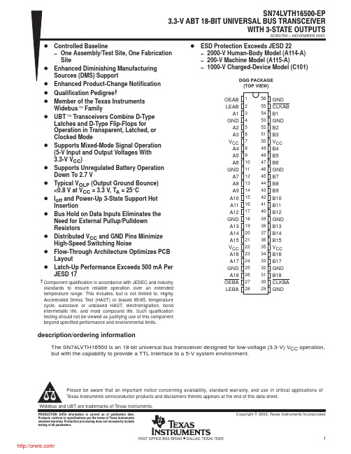
OEAB LEAB A1 GND A2 A3 VCC A4 A5 A6 GND A7 A8 A9 A10 A11 A12 GND A13 A14 A15 VCC A16 A17 GND A18 OEBA LEBA
1 2 3 4 5 6 7 8 9 10 11 12 13 14 15 16 17 18 19 20 21 22 23 24 25 26 27 28
description/ordering information (continued)
ORDERING INFORMATION
TA PACKAGE† ORDERABLE PART NUMBER TOP-SIDE MARKING
−40°C to 85°C TSSOP − DGG Tape and reel CLVTH16500IDGGREP LH16500EP † Package drawings, standard packing quantities, thermal data, symbolization, and PCB design guidelines are available at /sc/package.
SN74LVTH16500ĆEP 3.3ĆV ABT 18ĆBIT UNIVERSAL BUS TRANSCEIVER WITH 3ĆSTATE OUTPUTS
SCBS783 − NOVEMBER 2003
D Controlled Baseline D D D D D
− One Assembly/Test Site, One Fabrication Site Enhanced Diminishing Manufacturing Sources (DMS) Support Enhanced Product-Change Notification Qualification Pedigree† Member of the Texas Instruments Widebus Family UBT Transceivers Combine D-Type Latches and D-Type Flip-Flops for Operation in Transparent, Latched, or Clocked Mode Supports Mixed-Mode Signal Operation (5-V Input and Output Voltages With 3.3-V VCC) Supports Unregulated Battery Operation Down To 2.7 V Typical VOLP (Output Ground Bounce) <0.8 V at VCC = 3.3 V, TA = 25°C Ioff and Power-Up 3-State Support Hot Insertion Bus Hold on Data Inputs Eliminates the Need for External Pullup/Pulldown Resistors Distributed VCC and GND Pins Minimize High-Speed Switching Noise Flow-Through Architecture Optimizes PCB Layout Latch-Up Performance Exceeds 500 mA Per JESD 17
视频服务器T650配置
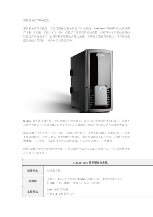
视频服务器T650配置
想要服务器的性能好,首先是要保证服务器的CPU性能好,Intel Xeon E5-2650V2处理器拥有8核16线程,而且L3为20M,保持了行业领先的功效优势,并将英特尔至强处理器的性能提升到更高水平,它利用基于硬件的内建功能进一步增强了数据保护能力,可在提高数据加密能力的同时,减少对于性能的影响。
Gisdom服务器使用可靠、大容量的高清硬盘性能,高清3.5寸硬盘经过专门设计,能够可靠地全天候运行。
经过优化,实现了低功耗、安静运行、流畅的视频流、高可靠性和大容量。
电源采用“双管正激”技术,保证了电源的绝对稳定。
双路12V输出,为CPU和显卡提供了强大的能量。
主动式PFC,功率因数达到99%,电源寿命超过10万小时。
电源转换率达到80%,节能省电,风扇采用双滚珠轴承技术,给您带来超静音的工作环境。
借助T650平衡高性能和高效管理。
办公环境所用塔式服务器的理想之选,亦可随着数据中心的增长进行扩展。
IBM磁带产品详细参数

10%到80%相对湿度(非冷凝)
功率
100V交流电压时为4.0amps;240V交流电压时为2.0amps 0.1 KVA
连接和系统支持
TS3200全高型提供了LVD SCSI、4Gbps光纤通道和3Gbps SAS接口。TS3200半高型提供LVD SCSI和3Gbps SAS接口,两种外形均可连接至IBM Power Systems、IBM System x、HP-UX、Sun Solaris、UNIX®、Linux®和Windows®服务器以及支持该接口规范的非IBM服务器、工作站和个人计算机。
Ultrium 3半高型:LVD SCSI(95P4998);3Gbps SAS(95P5000)
可用型号
3573 4UL:TS3200磁带库型号L4U无驱动器
可选功能代码
路径故障转移
45E9503
透明的LTO加密
45E3081
机架安装
23R6998
右侧磁带盒仓
左上侧磁带盒
左下侧磁带盒
23R6999
磁带系统
TS2900
驱动器选件
Ultrium 3半高型:3 Gbps SAS
Ultrium 4半高型:3 Gbps SAS
可用型号
PN 3572S3R(HH LTO3)
PN 3572S3E(带有桌面套件的HH LTO3)
PN 3572S4R(HH LTO4)
PN 3572S3E(带有桌面套件的HH LTO4)
每磁带库最高可达38.4 TB(压缩);本机为19.6 TB
每磁带库最高可达19.2 TB(压缩);本机为9.6 TB
数据传输速率
使用LTO Ultrium 4,本机数据传输速率可达120 MBps
ISL6505CRZ-T;ISL6505CRZ;ISL6505CB;ISL6505CB-T;ISL6505CR;中文规格书,Datasheet资料
®ISL6505Multiple Linear Power Controller with ACPI Control InterfaceThe ISL6505 complements other power building blocks (voltage regulators) in ACPI-compliant designs for microprocessor and computer applications. The IC integrates three linear controllers/regulators, switching, monitoring and control functions into a 20-pin wide-body SOIC or 20-pin QFN (also known as MLF) 5x5 package. The ISL6505’s operating mode (active or sleep outputs) is selectable through two digital control pins, S3 and S5.One linear controller generates the 3.3V DUAL/3.3V SB voltage plane from the A TX supply’s 5V SB output, powering the south bridge and the PCI slots through an external NPN pass transistor during sleep states (S3, S4/S5). In active state (during S0 and S1/S2), the 3.3V DUAL/3.3V SB linear regulator uses an external N-channel pass MOSFET to connect the outputs directly to the 3.3V input supplied by an A TX power supply, for minimal losses. The 3.3V DUAL/3.3V SB output is active for as long as the A TX 5V SB voltage is applied to the chip.A controller powers up the 5V DUAL plane by switching in the A TX 5V output through an NMOS transistor in active states, or by switching in the A TX 5V SB through a PMOS (or PNP) transistor in S3 sleep state. In S4/S5 sleep states, theISL6505 5V DUAL output is either shut down or stays on, based on the state of the EN5 pin.An internal linear regulator supplies the 1.2V for the voltage identification circuitry (VID) only during active states (S0 and S1/S2), and uses the 3V3 pin as input source for its internal pass element.A linear controller generates V OUT1 from the3.3V DUAL/3.3V SB voltage plane, using an external NFET. The voltage is user-programmable to values between 1.2V and 1.5V, using an external resistor divider. The mode is user-selectable with the LAN pin; a logic high (or open) selects the 10/100 LAN mode, where V OUT1 is always on (S0-S5); a logic low selects the Gigabit Ethernet mode, where V OUT1 is only on during active modes (S0-S2). Features•Provides four ACPI-Controlled Voltages-5V DUAL USB/Keyboard/Mouse- 3.3V DUAL/3.3V SB PCI/Auxiliary/LAN- 1.2V VID Processor VID Circuitry-V OUT1 (1.2V - 1.5V programmable) LAN/Ethernet•Excellent Output Voltage Regulation-All Outputs: ±2.0% over temperature (as applicable)•Small Size; Very Low External Component Count •Undervoltage Monitoring of All Outputs with Centralized FAULT Reporting and T emperature Shutdown•QFN Package:-Compliant to JEDEC PUB95 MO-220QFN - Quad Flat No Leads - Package Outline-Near Chip Scale Package footprint, which improvesPCB efficiency and has a thinner profile•Pb-Free Plus Anneal Available (RoHS Compliant) Applications•ACPI-Compliant Power Regulation for Motherboards Pinouts - See page6.Ordering InformationPART NUMBERTEMP.RANGE (°C)PACKAGEPKG.DWG. # ISL6505CB*0 to 7020 Ld Wide SOIC M20.3 ISL6505CR*0 to 7020 Ld 5x5 QFN L20.5x5 ISL6505CRZ*(Note 1)0 to 7020 Ld 5x5 QFN(Pb-free)L20.5x5 ISL6505EVAL1Evaluation Board (SOIC)ISL6505EVAL2Evaluation Board (QFN)Add “-T” suffix for tape and reel.NOTE:1.Intersil Pb-free plus anneal products employ special Pb-freematerial sets; molding compounds/die attach materials and100% matte tin plate termination finish, which are RoHScompliant and compatible with both SnPb and Pb-free soldering operations. Intersil Pb-free products are MSL classified atPb-free peak reflow temperatures that meet or exceed thePb-free requirements of IPC/JEDEC J STD-020.Simplified Power System DiagramTypical ApplicationFIGURE 2.+5V SB+3.3V IN+12V IN SX, EN5, LAN+5V IN 3.3V DUAL FAULTSHUTDOWN V GND5VSB+3.3V IN+5V SB VID_PGVID_CTDR1C CT_VIDISL6505+12V IN VID PGOODSLP_S3S3V OUT33.3V DUAL /3.3V SBC OUT3+5V IN C OUT4V OUT45V DUAL3V3DL 3V3DLSBQ2Q3Q4Q5DLA5VDLSBFAULT5VDLSS 1V2VID SHUTDOWNFAULT V OUT11.2V - 1.5VV OUT21.2V VIDC OUT1C OUT2SLP_S5S5C SS3V3R DLAQ6FB1LANEN5EN5LAN5V FIGURE 3.R20R21Absolute Maximum Ratings Thermal InformationSupply Voltage, V5VSB . . . . . . . . . . . . . . . . . . . . . . . . . . . . . . +7.0V DLA . . . . . . . . . . . . . . . . . . . . . . . . . . . . . . . . GND - 0.3V to +14.5V All Other Pins. . . . . . . . . . . . . . . . . . . . . . . . . . . . . . . . . . . . . .+ 7.0V ESD Classification (Human Body Model) . . . . . . . . . . . . . . . . . .2kV Recommended Operating ConditionsSupply Voltage, V5VSB . . . . . . . . . . . . . . . . . . . . . . . . . . . +5V ±5% Lowest 5VSB Supply Voltage Guaranteeing Parameters . . . . +4.5V Digital Inputs, V Sx . . . . . . . . . . . . . . . . . . . . . . . . . . . . . . .0 to +5.5V Ambient T emperature Range. . . . . . . . . . . . . . . . . . . . .0o C to 70o C Junction Temperature Range. . . . . . . . . . . . . . . . . . . .0o C to 125o C Thermal Resistance (T ypical)θJA (o C/W)θJC (o C/W) SOIC Package (Note 2). . . . . . . . . . . .65N/AQFN Package (Notes 3, 4) . . . . . . . . .355 Maximum Junction T emperature (Plastic Package) . . . . . . . .150o C Maximum Storage T emperature Range. . . . . . . . . . -65o C to 150o C Maximum Lead T emperature (Soldering 10s) . . . . . . . . . . . . .300o C (SOIC - Lead Tips Only)CAUTION: Stresses above those listed in “Absolute Maximum Ratings” may cause permanent damage to the device. This is a stress only rating and operation of the device at these or any other conditions above those indicated in the operational sections of this specification is not implied.NOTES:2.θJA is measured with the component mounted on a high effective thermal conductivity test board in free air. See Tech Brief TB379 for details.3.θJA is measured in free air with the component mounted on a high effective thermal conductivity test board with “direct attach” features. SeeTech Brief TB379.4.For θJC, the “case temp” location is the center of the exposed metal pad on the package underside.Electrical Specifications Recommended Operating Conditions, Unless Otherwise Noted Refer to Figures 1, 2 and 3 PARAMETER SYMBOL TEST CONDITIONS MIN TYP MAX UNITS VCC SUPPLY CURRENTNominal Supply Current I5VSB-6-mA Shutdown Supply Current I5VSB(OFF)V SS = 0.8V-4-mA POWER-ON RESET, SOFT-START, AND VOLTAGE MONITORS5VSB Rising POR Threshold 4.0 4.3 4.5V5VSB Falling POR Threshold 3.15 3.4 3.55V5VSB POR Hysteresis-0.9-V3V3 Rising Threshold 2.8 2.93 3.0V3V3 Falling Threshold 2.65 2.78 2.9V3V3 Hysteresis-150-mV5V Rising Threshold 4.25 4.4 4.5V5V Falling Threshold 4.0 4.15 4.3V5V Hysteresis-250-mV VID_PG Rising Threshold- 1.04-VVID_PG Hysteresis-50-mV VID_CT Charging Current I VID_CT V VID_CT = 0V-10-µA Soft-Start Current I SS-10-µA Soft-Start Shutdown Voltage Threshold V SD--0.8V LINEAR REGULATOR (V OUT1; DR1 and FB1 pins)V OUT1 Regulation V OUT1 = 1.2V to 1.5V-- 2.0%V OUT1 Nominal Voltage Level V OUT1Based on external resistors- 1.5-VV OUT1 Undervoltage Rising Threshold FB1 pin- 1.2-VV OUT1 Undervoltage Hysteresis FB1 pin-50-mV DR1 Output Drive Current I DR1V3V3DL = 3.3V-10-mA1.2V VID LINEAR REGULATOR (V OUT2)1V2VID Regulation-- 2.0%1V2VID Nominal Voltage Level V 1V2VID- 1.2-V 1V2VID Undervoltage Rising Threshold -0.92-V 1V2VID Undervoltage Hysteresis -100-mV 1V2VID Output CurrentI 1V2VIDV 3V3 = 3.3V--180mA3.3V DUAL /3.3V SB LINEAR REGULATOR (V OUT3)3V3DL Sleep State Regulation -- 2.0%3V3DL Nominal Voltage Level V 3V3DL- 3.3-V 3V3DL Undervoltage Rising Threshold - 2.62-V 3V3DL Undervoltage Hysteresis -150-mV 3V3DLSB Output Drive CurrentI 3V3DLSBV 5VSB = 5V3050-mA5V DUAL SWITCH CONTROLLER (V OUT4)5VDL Undervoltage Rising Threshold - 4.10-V 5VDL Undervoltage Hysteresis -120-mV 5VDLSB Output Drive Current I 5VDLSBV 5VDLSB = 4V , V 5VSB = 5V-20--40mATIMING INTERVALSActive State Assessment Past Input UV Thresholds (Note 5)425364ms Active-to-Sleep Control Input Delay -200-µs Falling UV Threshold Timeout (All Monitors)-10-µsCONTROL I/O (S3, S5, EN5, LAN, FAULT)High Level Input Threshold S3, S5, EN5, LAN -- 2.2V Low Level Input Threshold S3, S5, EN5, LAN 0.8--V Internal Pull-up Current to 5VSB S3, S5 to GND -50-µA Internal Pull-up Current to 5VSB EN5, LAN to GND -10-µA Input Leakage Current to 5VSB EN5, LAN to 5VSB --10mA FAULT Current IOH (to 5VSB)FAULT = 4.6V, 5VSB = 5V --7.5-mA FAULT Current IOL (to GND)FAULT = 0.4V, 5VSB = 5V-0.75-mATEMPERATURE MONITOR Fault-Level Threshold (Note 6)125--o C Shutdown-Level Threshold (Note 6)-155-o CNOTES:5.Guaranteed by Correlation.6.Guaranteed by Design.Electrical SpecificationsRecommended Operating Conditions, Unless Otherwise Noted Refer to Figures 1, 2 and 3 (Continued)PARAMETERSYMBOLTEST CONDITIONSMINTYPMAXUNITSFunctional Pin Description (Pin numbers for SOIC and QFN)3V3 (Pin 6 SOIC; Pin 3 QFN)Connect this pin to the A TX 3.3V output. This pin provides the output current for the 1V2VID pin, and is monitored for power quality.5V (Pin 7 SOIC; Pin 4 QFN)Connect this pin to the A TX 5V output. This pin is only monitored for power quality.5VSB (Pin 20 SOIC; Pin 17 QFN)Provide a very well de-coupled 5V bias supply for the IC to this pin by connecting it to the A TX 5V SB output. This pin provides all the chip’s bias as well as the base current for Q2 (see typical application diagram). The voltage at this pin is monitored for power-on reset (POR) purposes.GND (Pin 11 SOIC; Pin 8 QFN)Signal ground for the IC. All voltage levels are measured with respect to this pin.S3 and S5 (Pins 9, 10 SOIC; Pins 6, 7 QFN)These pins switch the IC’s operating state from active (S0, S1/S2) to S3 and S4/S5 sleep states. These are digital inputs featuring internal 50µA (typical) current source pull-ups to 5VSB. Internal circuitry de-glitches these pins for disturbances lasting as long as 2µs (typically). Additional circuitry blocks illegal state transitions (such as S4/S5 to S3), but does allow S3 to S4/S5. Connect S3 and S5respectively to the computer system’s SLP_S3 and SLP_S5 signals.EN5 (Pin 8 SOIC; Pin 5 QFN)This digital input selects whether the 5VDL output stays up or shuts down during the S5 Sleep Mode. It has a 10µA typical pull-up current source. A logic high (5V) or open will keep the 5VDL on during S5; a logic low (GND) will shut it off during S5. NOTE: This pin should be tied low or high (or open) on the board; it was not designed to be changed during normal operation.LAN (Pin 16 SOIC; Pin 13 QFN)This digital input selects between two modes for the V OUT1 regulator. It has a 10µA pull-up current source. A logic high (5V) or open selects the 10/100 LAN mode, where V OUT1 stays on all of the time (active and sleep modes). A logic low (GND) selects the Gigabit Ethernet mode, where V OUT1 is only on during active (S0, S1) modes. Note that thisselection is independent of the voltage selection of V OUT1 (which is determined by the external resistor divider). NOTE: This pin should be tied low or high (or open) on the board; it was not designed to be changed during normal operation.FAULT (Pin 12 SOIC; Pin 9 QFN)This digital output pin is used to report the fault condition by being pulled to 5VSB (pulled to GND if no fault). It is aCMOS digital output; an external pull-down resistor is NOT required. In case of an undervoltage on any of the controlled outputs, on any of the monitored A TX voltages (3V3 or 5V; not 12V), or in case of an overtemperature event, this pin is used to report the fault condition.PinoutsISL6505 (20 LEAD WIDE SOIC)TOP VIEWISL6505 (5X 5 QFN)TOP VIEWNOTE:The QFN bottom pad is electrically connected to the IC substrate, at GND potential. It can be left unconnected, or connected to GND; do NOT connect to another potential.1112131415161718201910987654321FB1DR13V3DLSB 3V3DL 1V2VID3V3EN55V S3S55VSB VID_PG SS LAN VID_CT 5VDL 5VDLSB DLA FAULT GND3V 3D L S B3V3DL 5V 1V2VID3V3D R 1F B 1F A U L T5VDL 5VDLSB5V S BS 3D L AEN5S 5G N DSSV I D _C T LAN VID_PG 1234567891015141312112019181716SS (Pin 17 SOIC; Pin 14 QFN)Connect this pin to a small ceramic capacitor (no less than 5nF; 0.1µF recommended). The internal soft-start (SS) current source along with the external capacitor creates a voltage ramp used to control the ramp-up of the output voltages. Pulling this pin low (to GND) with an open-drain device shuts down all the outputs as well as forces the FAULT pin low. The C SS capacitor is also used to provide a controlled voltage slew rate during active-to-sleep transitions on the 3.3V DUAL/3.3V SB output.3V3DL (Pin 4 SOIC; Pin 1 QFN)Connect this pin to the 3.3V dual/stand-by output (V OUT3). In sleep states, the voltage at this pin is regulated to 3.3V; in active states, A TX 3.3V output is delivered to this node through a fully-on NFET transistor. During all operating states, this pin is monitored for undervoltage events. This pin provides all the output current delivered by V OUT1.3V3DLSB (Pin 3 SOIC; Pin 20 QFN)Connect this pin to the base of a suitable NPN transistor. In sleep state, this transistor is used to regulate the voltage at the 3V3DL pin to 3.3V.DLA (Pin 13 SOIC; Pin 10 QFN)This pin is an open-collector output. Connect a 1kΩ resistor from this pin to the A TX 12V output. This resistor is used to pull the gates of suitable NFETs to 12V, which in active state, switch in the A TX 3.3V and 5V outputs into the3.3V DUAL/3.3V SB and 5V DUAL outputs, respectively.5VDL (Pin 15 SOIC; Pin 12 QFN)Connect this pin to the 5V DUAL output (V OUT4). In either operating state (when on), the voltage at this pin is provided through a fully-on MOSFET transistor. This pin is also monitored for undervoltage events.5VDLSB (Pin 14 SOIC; Pin 11 QFN)Connect this pin to the gate of a suitable PFET or bipolar PNP. This transistor is switched on, connecting the A TX5V SB output to the 5V DUAL regulator output during S3, and if EN5 is open or high, during S5. If EN5 is low (GND), the transistor is switched off in S5.DR1 (Pin 2 SOIC; Pin 19 QFN)This output pin drives the gate of an external NFET transistor to create V OUT1, which draws its output current from the 3V3DL pin.FB1 (Pin 1 SOIC; Pin 18 QFN)This analog input pin looks at the V OUT1 external resistor divider, and compares it to the internal reference (0.8V nominal), in order to regulate the voltage on V OUT1. This pin is also monitored for undervoltage events.1V2VID (Pin 5 SOIC; Pin 2 QFN)This pin is the output of the internal 1.2V voltage identification (VID) regulator (V OUT2). This internal regulator operates only in active states (S0, S1/S2) and is shut off during any sleep state. This regulator draws its output current from the 3V3 pin. This pin is monitored for undervoltage events.VID_PG (Pin 18 SOIC; Pin 15 QFN)This pin is the open collector output of the 1V2VID power good comparator. Connect a 10kΩ pull-up resistor from this pin to the 1V2VID output. As long as the 1V2VID output is below its PG threshold (typically 90% of final value), this pin is pulled low. Once the PG threshold is reached, the VID_CT pin starts charging its capacitor (setting the delay); when it reaches its trip point, then the VID-PG pin releases, and goes high (through the external pull-up resistor).VID_CT (Pin 19 SOIC; Pin 16 QFN)Connect a small capacitor from this pin to ground. The capacitor is used to delay the VID_PG reporting the 1V2VID has reached power good limits.DescriptionOperationThe ISL6505 controls 4 output voltages (Refer to Figures 1, 2, and 3). It is designed for microprocessor computer applications with 3.3V, 5V, 5V SB, and 12V bias input from an A TX power supply. The IC is composed of three linear controllers/regulators supplying the computer system’sV OUT1 (1.2V - 1.5V programmable), 3.3V SB and PCI slots’ 3.3V AUX power (V OUT3), the 1.2V VID circuitry power(V OUT2), a dual switch controller supplying the 5V DUAL voltage (V OUT4), as well as all the control and monitoring functions necessary for complete ACPI implementation.Initialization and PORThe ISL6505 automatically initializes upon receipt of input power. The Power-On Reset (POR) function continually monitors the 5V SB input supply voltage, initiating3.3V DUAL/3.3V SB and 1.5V SB soft-start operation shortly after exceeding POR threshold.Note that while the 5VSB pin has the main POR, both the3V3 and 5V pins (12V is not monitored) must rise above their own POR levels (typically 90%) in order to transition into the S0/S1 active state. If during normal operation either one drops below their falling trip points, the IC will go to the S5 sleep mode. When both are back above their rising thresholds, the IC will again soft-start into active state.Output Operational Truth TablesTable 1 describes the truth combinations pertaining to the 3.3V DUAL/SB and 5V DUAL dual outputs. The last two lines highlight the difference between EN5 connected high or low.Table 2 describes the truth combinations pertaining to the V OUT1 (typically between 1.2V and 1.5V) and 1V2VID outputs. The last two sets of lines highlight the difference between the two LAN pin modes (5V/open is the 10/100 LAN mode; GND is the Gigabit Ethernet mode).The internal circuitry does not allow the transition from an S4/S5 (suspend to disk/soft off) state to an S3 (suspend to RAM) state; however, it does allow the transition from S3 to S4/S5. The only ‘legal’ transitions are from an active state (S0, S1) to a sleep state (S3, S5) and vice versa.Functional Timing DiagramsFigures 4 (EN5 = low), 5 (EN5 = high), and 6 are timing diagrams, detailing the power up/down sequences of all the outputs in response to the status of the sleep-state pins (S3, S5), as well as the status of the input A TX supply . Not shown in these diagrams is the deglitching feature used to protect against false sleep state tripping. Both S3 and S5 pins are protected against noise by a 2µs filter (typically 1–4µs). This feature is useful in noisy computer environments if the control signals have to travel over significant distances. Additionally , the S3 pin features a 200µs delay in transitioning to sleep states. Once the S3 pin goes low, an internal timer is activated. At the end of the 200µs interval, if the S5 pin is low, the ISL6505 switches into S5 sleep state; if the S5 pin is high, the ISL6505 goes into S3 sleep state.The shaded column in Figures 4 and 5 highlights thedifference on the 5VDLSB and 5VDL pins for the two EN5 states.TABLE 1.5V DUAL OUTPUT (V OUT4) AND 3.3VDL/SB (V OUT3)TRUTH TABLE S5S3 3.3VDL/SB5VDL COMMENTS 11 3.3V 5V S0/S1/S2 States (Active)10 3.3V5VS301NoteMaintains Previous State00 3.3V 0V S4/S5 (EN5 = GND)03.3V 5V S4/S5 (EN5 = open/5V)NOTE:Combination Not Allowed.TABLE 2.V OUT1 AND 1V2VID (V OUT2) TRUTH TABLE S5S3V OUT11V2VID COMMENTS 11 1.5V 1.2V S0/S1/S2 States (Active)100V 0V S3 (LAN = GND)10 1.5V0VS3 (LAN = open/5V)01NoteMaintains Previous State 000V 0V S4/S5 (LAN = GND)01.5V 0V S4/S5 (LAN = open/5V)NOTE:Combination Not Allowed.FIGURE 4.5V DUAL AND 3.3V DUAL /3.3V SB TIMINGDIAGRAM; EN5 = GND5VSB 3.3V, 5V S3S55VDLSBDLA 3V3DLSB3V3DL5VDLFIGURE 5.5V DUAL AND 3.3V DUAL /3.3V SB TIMINGDIAGRAM; EN5 = 5V/OPEN5VSB 3.3V, 5V S3S55VDLSB DLA 3V3DLSB3V3DL5VDLFIGURE 6.V OUT1 AND 1.2V VID TIMING DIAGRAM (NOTETHE DEPENDENCE OF V OUT1 ON THE LOGIC STATE OF LAN PIN)5VSB 3.3V,S3S51V2VIDDLA V OUT15V, 12V (LAN=5V)V OUT1 (LAN=GND)Soft-Start into Sleep States (S3, S4/S5)The 5V SB POR function initiates the soft-start sequence. An internal 10µA current source charges an external capacitor. The error amplifiers’ reference inputs are clamped to a level proportional to the SS (soft-start) pin voltage. As the SS pin voltage slews from about 1.4V to 3.0V , the input clamp allows a rapid and controlled output voltage rise.Figures 7 (EN5 = low) and 8 (EN5 = high) show the soft-start sequence for the typical application start-up into a sleep state. At time T0 5V SB (bias) is applied to the circuit. At time T1, the 5V SB surpasses POR level. An internal fast charge circuit quickly raises the SS capacitor voltage toapproximately 1V , then the 10µA current source continues the charging.The soft-start capacitor voltage reaches approximately 1.4V at time T2, at which point the 3.3V DUAL /3.3V SB and V OUT1 error amplifiers’ reference inputs start their transition, resulting in the output voltages ramping up proportionally. The ramp-up continues until time T3 when the two voltages reach the set value. As the soft-start capacitor voltage reaches approximately 3.0V , the undervoltage monitoring circuit of this output is activated and the soft-start capacitor is quickly discharged to approximately 1.4V . Following the 3ms (typical) time-out between T3 and T4, the soft-start capacitor commences a second ramp-up designed tosmoothly bring up the remainder of the voltages required by the system. At time T5, voltages are within regulation limits, and as the SS voltage reaches 3.0V , all the remaining UV monitors are activated and the SS capacitor is quicklydischarged to 1.4V , where it remains until the next transition. As the 1.2V VID output is only on while in an active state, it does not come up, but rather waits until the main A TX outputs come up within regulation limits.Note that in Figures 7 and 8, LAN = 5V/open. If the LAN pin is connected to GND instead, then the V OUT1 output does not turn on at all in either sleep mode (S3 or S4/S5).Soft-Start into Active States (S0, S1)If both S3 and S5 are logic high at the time the 5V SB is applied, the ISL6505 will assume active state wake-up and keep off the required outputs until some time (typically 50ms) after the monitored main A TX outputs (3.3V and 5V; 12V is not monitored here) exceed the set thresholds. This time-out feature is necessary in order to ensure the main A TX outputs are stabilized. The time-out also assures smooth transitions from sleep into active when sleep states are being0V0VTIMESOFT-START (1V/DIV)OUTPUT (1V/DIV)VOLTAGES V OUT1V OUT4 (5V DUAL ) if S3T1T2T3T05V SB (1V/DIV)T5T4V OUT3 (3.3V DUAL /3.3V SB )V OUT2(1.2V VID )V OUT4 (5V DUAL ) if S5FIGURE 7.SOFT -START INTERVAL IN A SLEEP STATE; EN5= GND; LAN = 5V/OPEN0V0VSOFT-START (1V/DIV)OUTPUT (1V/DIV)VOLTAGES V OUT1V OUT4 (5V DUAL )T1T2T3T05V SB (1V/DIV)T5T4V OUT3 (3.3V DUAL /3.3V SB )V OUT2(1.2V VID )FIGURE 8.SOFT -START INTERVAL IN A SLEEP STATE;EN5 = 5V/OPEN; LAN = 5V/OPENTIMEsupported. 3.3V DUAL /3.3V SB and V OUT1 outputs will come up right after bias voltage surpasses POR level (but if LAN = GND, then V OUT1 output will not come up until the soft-start ramp, along with V OUT2; see Figure 9).During sleep-to-active state transitions from conditionswhere the 5V DUAL output is initially GND (such as S5 to S0 transition, or simple power-up sequence directly into active state), the circuit goes through a quasi soft-start, the5V DUAL output being pulled high through the body diode of the NMOS FET connected between it and the 5V A TX. Figure 9 exemplifies this start-up case. 5V SB is already present when the main A TX outputs are turned on, at time T0. As a result of +5V IN ramping up, the 5V DUAL output capacitors charge up through the body diode of Q5 (see T ypical Application). At time T1, all main A TX outputs exceed the ISL6505’s undervoltage thresholds, and the internal 50ms (typical) timer is initiated. At T2, the time-out initiates a soft-start, and the 1.2V voltage ID output is ramped-up, reaching regulation limits at time T3. Simultaneous with the beginning of this ramp-up, at time T2, the DLA pin isreleased, allowing the pull-up resistor to turn on Q3 and Q5, and bring the 5V DUAL output in regulation. Shortly after time T3, as the SS voltage reaches 3.0V , the soft-start capacitor is quickly discharged down to approximately 2.7V , where it remains until a valid sleep state request is received from the system.Fault ProtectionAll of the outputs are monitored against undervoltage events. A severe overcurrent caused by a failed load on any of the outputs, would, in turn, cause that specific output tosuddenly drop. If any of the output voltages drops below 80% (typical) of their set value, such event is reported by having the FAULT pin pulled to 5V . Additionally, exceeding the maximum current rating of an integrated regulator (output with pass transistor on-chip) can lead to output voltage drooping; if excessive, this droop can ultimately trip the undervoltage detector and send a FAULT signal to the computer system.A FAULT condition occurring on an output when controlled through an external pass transistor will only set off theFAULT flag, and it will not shut off or latch off any part of the circuit. A FAULT condition occurring on an output controlled through an internal pass transistor (1V2VID only), will set off the FAULT flag, and it will shut off the respective faulting regulator (1V2VID only). If shutdown or latch off of the entire circuit is desired in case of a fault, regardless of the cause, this can be achieved by externally pulling or latching the SS pin low. Pulling the SS pin low will also force the FAULT pin to go low and reset any internally latched-off output.Special consideration is given to the initial start-upsequence. If, following a 5V SB POR event, any of the V OUT1 or 3.3V DUAL /3.3V SB outputs is ramped up and is subject to an undervoltage event before the end of the second soft-start ramp, then the FAULT output goes high and the entire IC latches off. Latch-off condition can be reset by cycling the bias power (5V SB ). Undervoltage events on the V OUT1 and the 3.3V DUAL /3.3V SB outputs at any other times are handled according to the description found in the second paragraph under the current heading.Another condition that could set off the FAULT flag is chip overtemperature. If the ISL6505 reaches an internaltemperature of 140o C (typical), the FAULT flag is set, but the chip continues to operate until the temperature reaches 155o C (typical), when unconditional shutdown of all outputs takes place. Operation resumes only after powering down the IC (to create a 5V SB POR event) and a start-up(assuming the cause of the fault has been removed; if not, as it heats up again, it will repeat the FAULT cycle).In ISL6505 applications, loss of the active A TX output (3V3 or 5V , as detected by the on-board voltage monitor) during active state operation causes the chip to switch to S5 sleep state, in addition to reporting the input UV condition on the FAULT pin. Exiting from this forced S5 state can only be achieved by returning the faulting input voltage above its UV threshold, by resetting the chip through removal of 5V SB bias voltage, or by bringing the SS pin at a potential lower than 0.8V .FIGURE 9.SOFT -START INTERVAL IN ACTIVE STATETIMET1T2T3T0分销商库存信息:INTERSILISL6505CRZ-T ISL6505CRZ ISL6505CB ISL6505CB-T ISL6505CR ISL6505CR-T。
Relion 650 Series RET650 变压器保护设备说明书
inputs) and up to four binary input/output modules −− 20 analog inputs (selected combinations of CT/VT
inputs) and up to two binary input/output modules • Power supply modules from 24 to 30 V DC, 48 to 250 V
Most important protection functions • Transformer differential protection
−− Percentage bias restraint −− Waveform and second harmonic restraint for
transformer inrush −− Fifth harmonic restraint for overexcitation −− Automatic CT ratio matching and vector group
Transformer protection RET650 Relion® 650 series Ver. 1.3
Features • Fully IEC 61850 compliant • Parallel Redundancy Protocol (PRP) according to IEC
62439-3 Ed.2 • Protection, control and monitoring integrated in one IED • Extensive self-supervision including analog channels • Four independent parameter setting groups • Large HMI for visualization of single line diagrams and
REGATRON G5.BT系列电池测试仪说明书

G5.BT Battery Tester SeriesThe G5.BT series is bidirectional regenerative. It was developed specifically for testing energy storage devices and is suitable for use in laboratories and on test benches. The modular and finely graded G5.BT series is characterized by highly dynamic response times and a wide cur-rent-voltage range with an auto-ranging factor 3. The G5.BT series has an outstanding current accuracy of <0.02% FS, an additional high-resolution current measurement range, and a fast current rise time in the 100 μs range. Ripple modulation, an integrated safety relay for PL c according to EN ISO 13849 and a powerful CAN multi-protocol interface (1 kHz, 16 bit) as well as functions to avoid reverse-polarity problems, current surges, and unwanted deep discharg-es make the G5.BT series the ideal, versatile battery module and battery pack tester.Device TypesVoltage V Power kW Current A Height U Order Code 0...500 18 -108...108 4 G5.BT.18.500.108 0...500 27 -162...162 7 G5.BT.27.500.162 0...500 36 -216 (216)7 G5.BT.36.500.216 0…500 54 -324…324 10 G5.BT.54.500.324 0…1000 18 -54…54 4 G5.BT.18.1000.54 0…1000 36 -108…108 7 G5.BT.36.1000.108 0…1000 54 -162…162 10 G5.BT.54.1000.162 0…1500 27 -54…54 7 G5.BT.27.1500.540…1500 54 -108…108 10 G5.BT.54.1500.108Modular and Easy Scalable SystemsThe output of an individual power supply is in the range from 0...18 kW to 0...2000+ kW, up to 3000 VDC. The advantageous modularity of REGATRON power supply solutions allows the system to be easily adapted to ever changing test requirements. Not only is it possible to reconfigure between parallel, series, and mixed operation, but also to expand the systemwith additional power supply units or to split it intosmaller units.Therefore, the purchase of a REGATRON power supply is a solid investment for the future.Figure 1: Modular concept for easy power and voltage increase by parallel, series, and mixed operation. The parallel configuration allows even an operation of different power levels, e.g., 18, 36, and 54 kW modules, in one system.Whether for single devices or powerful multi-device master-slave systems, REGATRON also offers turn-key cabinet solutions or project specific system integration according to customer specifications. Battery Module/Pack-Testing FeaturesThe G5.BT series has an exceptional electrical performance that offers several advantages for battery testing applications:▪Accuracy of <0.02% FS▪Additional high-resolution currentmeasurement range from -10 to 10% FS ▪Current rise time in the 50…200 µs range▪Parameterizable to avoid overshoot▪Current ripple modulation up to 10 kHzIn addition, the G5.BT provides important features for user safety, power supply, and battery protection. It avoids:▪Reverse-polarity problems▪Arcing and high inrush current whenconnecting the battery to the DC terminalseven at unmatched voltage levels▪Deep battery discharge at voltage off state (DC port impedance >10 MΩ)Features such as adjustable controller settings and the integrated powerful 8-channel digital scope assist the user to quickly and easily achieve optimal system behavior for a special application requirement. The G5.BT series also offers the possibility to store, edit and recall any device configuration on board the power supply.DynamicsMaximum speed or minimum overshoot? Figure 2 shows that the dynamic parameters of the G5.BT series can be easily adapted to a specific task.Figure 2: Parameterization example: set-value step currents. -97…97 A@333VDC in <50 µs with overshoot (top), in <200 µs w/o overshoot (bottom). General Dynamic DataInterfacesCAN InterfaceThe CAN multi-protocol (CANmp) interface has a 1 kHz data rate, a 16-bit resolution and is adaptable to any proprietary CAN bus. In addition, it supports dbc file handling.Integrated Safety RelayIntegrated safety relay (ISR) for increased emergency stop reliability supporting performance level PL c / PL e according to EN ISO 13849.Control ModesCV constant voltageCC constant currentCP constant powerCR constant resistanceRi internal resistance simulationSystem ControlG5.Control operating and maintenance software API .NET programming, e.g., by LabView,Python, Matlab, or REST interface I/O port Analog interface for set and actualvalues, operating statesGrid ConnectionThe wide-band AC input accepts all common AC grid systems and has an active power factor correction.AC Grid 380…480 VAC ±10% at 50/60 HzPF 0.99Efficiency 95…96%OptionsSoftware and ControlBatControlThe battery tester is controlled by interfaces such as CANmp for the integration into automated test benches or by the optional application software BatControl for R+D applications in the laboratory. BatControl allows selecting and running so-called BatScripts. These scripts automate the manually given commands to the G5 Battery Tester and allow the running of these commands according to defined schedules.▪Define charge and discharge algorithms▪Run drive cycles (according to own or already defined standards)▪Repeat previously recorded discharge/charge dataTime-Based Function GeneratorThe TFE time-based function generator allows programming either through G5.Control operating software, HMI touch display, or CANmp interface.▪Time-dependent functions U = f(t), I = f(t), P = f(t): sine, triangle, or square as well as user-defined data points. Import and exportthrough csv files supported▪Sweep function for current ripple modulation 0…10 kHzHMIThe HMI built into the front panel allows compre-hensive and convenient operation of the power supply via touch display.Figure 3: Intuitive control by HMI touch display. Everything you need at a glance. User Safety▪Discharge of AC filter (XCD), recommended for mobile use of the device. XCD ensures adischarge time of the AC filter <1 s requiredby EN 50178▪AC terminal protection cover (PAC.AC),recommended for use as tabletop unitRack-Integrated System Solutions▪Mobile rack solutions up to IP54▪Insulation monitoring: remote activation of the insulation measurement, actual insulation valueand warning/error status are provided byCANmp interface or by optional HMI▪Easy reconfiguration between parallel, series, and mixed operationFigure 4: REGATRON’s rack-integrated turn-key system solutions, e.g., 72 kW (left) and 162 kW (right) power levels. Various types of AC/DC connectors and cables allow for comfortable handling. Third-party product integration and numerous safety options are additional features.Environmental ConditionsFront-panel-mounted air filter (AirFilter), recom-mended for use in dusty environments.NEWDC Generation 5REGATRON DC & AC Power Supplies: Modular ∙ Precisely Engineered ∙ Technologically AdvancedImportant Features of the G5.BT SeriesTechnology▪ Technologically advanced, fast switching,compact 19-inch power supplies▪ High control dynamics in the 100...200 µsrange – even at higher power levels▪ Exceptional accuracy of <0.02% FS, additionalhigh-resolution measurement range ▪ Wide current-voltage range with an auto-ranging factor 3▪ CV, CC, CP, CR, and Ri-Sim control modes ▪ Regenerative and highly efficient, resulting insignificant reduction of energy consumption and heat dissipationSystem Capability▪ Modular and easy scalable systems▪ Parallel, series, and mixed operation with adigital high-speed bus▪ Simple master-slave configuration with theoperating software ▪ Easy rack mounting▪ Optional safety features such as 2-channelsafety interface and insulation monitoring ▪ Turn-key cabinet solutions or project-specificsystem integration according to customer specificationSystem Control and Options▪ Operating software, extended analysis, andparameterization options, calibration ▪ Application software with visualization,programming, and data logger▪ Powerful application programming interfaces(APIs)******************All product specifications and information herein are provisional and subject to change without notice. Filename: PD_G5.BT_EN_201007.docxnd ***************************************.com。
瑞特拉电子产品购买指南说明书
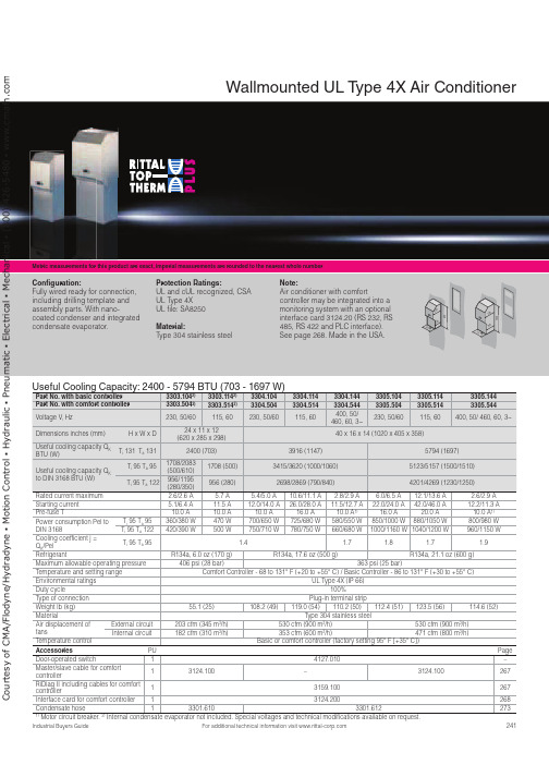
241For additional technical information visit Metric measurements for this product are exact, imperial measurements are rounded to the nearest whole numberUseful Cooling Capacity: 2400 - 5794 BTU (703 - 1697 W)Part No. with basic controller 3303.1042)3303.1142)3304.1043304.1143304.1443305.1043305.1143305.144Part No. with comfort controller 3303.5042)3303.5142)3304.5043304.5143304.5443305.5043305.5143305.544Voltage V , Hz230, 50/60115, 60230, 50/60115, 60400, 50/ 460, 60, 3~230, 50/60115, 60400, 50/ 460, 60, 3~Dimensions inches (mm)H x W x D24 x 11 x 12 (620 x 285 x 298)40 x 16 x 14 (1020 x 405 x 358)Useful cooling capacity Q KBTU (W)T i 131 T a 1312400 (703)3916 (1147)5794 (1697)Useful cooling capacity Q K to DIN 3168 BTU (W)T i 95 T a 951708/2083(500/610)1708 (500)3415/3620 (1000/1060)5123/5157 (1500/1510)T i 95 T a 122956/1195(280/350)956 (280)2698/2869 (790/840)4201/4269 (1230/1250)Rated current maximum 2.6/2.6 A 5.7 A 5.4/5.0 A 10.6/11.1 A 2.8/2.9 A 6.0/6.5 A 12.1/13.6 A 2.6/2.9 A Starting current 5.1/6.4 A 11.5 A 12.0/14.0 A 26.0/28.0 A 11.5/12.7 A 22.0/24.0 A 42.0/46.0 A 12.2/11.3 A Pre-fuse T 10.0 A 10.0 A 10.0 A 16.0 A 10.0 A 1)16.0 A 20.0 A 10.0 A 1)Power consumption Pel toDIN 3168T i 95 T a 95360/380 W 470 W 700/650 W 725/680 W 580/550 W 850/1000 W 880/1050 W 800/980 W T i 95 T a 122420/390 W500 W 750/710 W 780/750 W 660/680 W 1000/1160 W 1040/1200 W 960/1150 W Cooling coefficient j =Q K /PelT i 95 T a 95 1.4 1.7 1.8 1.7 1.9Refrigerant R134a, 6.0 oz (170 g)R134a, 17.6 oz (500 g)R134a, 21.1 oz (600 g)Maximum allowable operating pressure 406 psi (28 bar)363 psi (25 bar)Temperature and setting range Comfort Controller - 68 to 131° F (+20 to +55° C) / Basic Controller - 86 to 131° F (+30 to +55° C)Environmental ratings UL Type 4X (IP 66)Duty cycle 100%Type of connection Plug-in terminal strip Weight lb (kg)55.1 (25)108.2 (49)119.0 (54)110.2 (50)112.4 (51)123.5 (56)114.6 (52)Material Type 304 stainless steelAir displacement offans External circuit 203 cfm (345 m 3/h)530 cfm (900 m 3/h)530 cfm (900 m 3/h)Internal circuit 182 cfm (310 m 3/h)353 cfm (600 m 3/h)471 cfm (800 m 3/h)Temperature control Basic or comfort controller (factory setting 95° F [+35° C])Accessories PU Page Door-operated switch 14127.010–Master/slave cable for comfortcontroller13124.100–3124.100267RiDiag II including cables for comfortcontroller13159.100267Interface card for comfort controller 13124.200268Condensate hose 13301.6103301.6122731) Motor circuit breaker. 2)Internal condensate evaporator not included. Special voltages and technical modifications available on request.Wallmounted UL T ype 4X Air ConditionerCon guration:Fully wired ready for connection, including drilling template and assembly parts. With nano-coated condenser and integrated condensate evaporator.Protection Ratings:UL and cUL recognized, CSA UL Type 4XUL file: SA8250 Material:Type 304 stainless steel Note:Air conditioner with comfortcontroller may be integrated into a monitoring system with an optional interface card 3124.20 (RS 232, RS 485, RS 422 and PLC interface). See page 268. Made in the USA.000C o u r t e s y o f C M A /F l o d y n e /H y d r a d y n e ŀ M o t i o n C o n t r o l ŀ H y d r a u l i c ŀ P n e u m a t i c ŀ E l e c t r i c a l ŀ M e c h a n i c a l ŀ (800) 426-5480 ŀ w w w .c m a f h .c o242For additional technical information visit Metric measurements for this product are exact, imperial measurements are rounded to the nearest whole numberUseful Cooling Capacity: 8706 - 10525 BTU (2550 - 3083 W)Part No. with basic controller 3328.1043328.1143328.1443329.1043329.1143329.144Part No. with comfort controller 3328.5043328.5143328.5443329.5043329.5143329.544Rated operating voltage V , Hz 230, 50/60115, 50/60400, 50/460, 60, 3~230, 50/60115, 50/60400, 50/460, 60, 3~Dimensions inches (mm)H x W x D 65 x 16 x 15 (1650 x 405 x 388)Useful cooling capacity Q K BTU (W)T i 131 T a 1318706 (2550)10525 (3083)Useful cooling capacity Q K to DIN 3168 BTU (W)T i 95 T a 956860/8025 (2000/2350)8538/9392 (2500/2750)T i 95 T a 1224952/5772 (1450/1690)5464/5977 (1600/1750)Rated current max. 7.5 A/9.1 A 14.7 A/17.3 A 2.8 A/3.3 A 8.6 A/10.6 A 17.0 A/22.0 A 3.7 A/3.8 A Start-up current 22.0 A/26.0 A36.0 A/39.0 A6.8 A/7.8 A 21.0 A/21.0 A44.0 A/42.0 A6.8 A/7.6 A Pre-fuse T16.0 A25.0 A 10.0A/10.0 A 1)16.0 A 25.0 A 10.0 A/10.0 A 1)Power consumption Pel to DIN 3168 T i 95 T a 951025/1200 W 1085/1250 W 1050/1275 W 1450/1675 W 1500/1725 W 1425/1625 W T i 95 T a 1221250/1350 W1300/1410 W1275/1525 W1625/2000 W1675/2065 W1675/1975 WCooling coefficient j = Q K /Pel T i 95 T a 951.72.31.92.0RefrigerantR134a, 31.7 oz (900 g)Maximum allowable operating pressure 406 psi (28 bar)Temperature and setting range Comfort Controller - 68 to 131° F (+20 to +55° C) / Basic Controller - 86 to 131° F (+30 to +55° C)Protection rating UL Type 4X (IP 66)Duty cycle 100%Type of connection Plug-in terminal stripWeight lb (kg)176.4 (80)191.8 (87)176.4 (80)183.0 (83)198.4 (90)183.0 (83)MaterialType 304 stainless steelAir displacement of fans External circuit 377 cfm (640 m 3/h)418 cfm (710 m 3/h)Internal circuit324 cfm (550 m 3/h)377 cfm (640 m 3/h)Temperature control Basic or comfort controller (factory setting 95° F [+35° C])Accessories PU Page Door-operated switch14127.010–Master/slave cable for comfort controller13124.100267RiDiag II including cables for comfort controller 13159.100267Interface card for comfort controller 13124.200268Condensate hose13301.6122731)Motor circuit breaker. Special voltages available on request. We reserve the right to make technical modifications.Wallmounted UL T ype 4X Air ConditionerCon guration:Fully wired ready for connection, including drilling template and assembly parts. With nano-coated condenser and integrated condensate evaporator.Protection Ratings: UL and cUL recognized UL Type 4X UL file: SA8250Material:Type 304 stainless steelNote:Air conditioner with comfortcontroller may be integrated into a monitoring system with an optional interface card 3124.200(RS 232, RS 485, RS 422 and PLC interface). See page 268. Made in the USA.C o u r t e s y o f C M A /F l o d y n e /H y d r a d y n e ŀ M o t i o n C o n t r o l ŀ H y d r a u l i c ŀ P n e u m a t i c ŀ E l e c t r i c a l ŀ M e c h a n i c a l ŀ (800) 426-5480 ŀ w w w .c m a f h .c o。
RF650中文资料
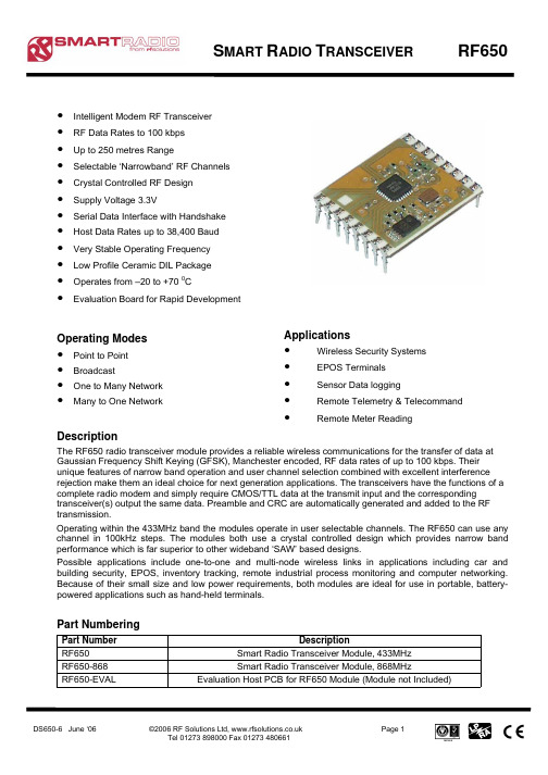
DS650-6 June ‘06©2006 RF Solutions Ltd, Page 1Tel 01273 898000 Fax 01273 480661S MART R ADIO T RANSCEIVER RF650ApplicationsWireless Security Systems 元器件交易网DS650-6 June ‘06©2006 RF Solutions Ltd, Page 2Tel 01273 898000 Fax 01273 480661S MART R ADIO T RANSCEIVER RF650Table Of Contents1 M o d u l e C o n n e c t i o n s ................................................................................................................3 2O p e r a t i o n .................................................................................................................................4 2.1 O p e r a t i o n M o d e s ..............................................................................................................4 2.2 S e r i a l D a t a F o r m a t ...........................................................................................................4 2.3 C T S t i m i n g .......................................................................................................................4 3 C o n f i g u r a t i o n ...........................................................................................................................5 3.1 S o f t w a r e C o n f i g u r a t i o n ....................................................................................................6 4 A p p l i c a t i o n I n f o r m a t i o n ............................................................................................................7 4.1 A p p l i c a t i o n S c h e m a t i c ......................................................................................................7 4.2 A n t e n n a D e s i g n ................................................................................................................8 5 T e c h n i c a l S p e c i f i c a t i o n s ..........................................................................................................9 5.1 M e c h a n i c a l D e t a i l .............................................................................................................9 6 E v a l u a t i o n B o a r d ...................................................................................................................10 6.1 C o n n e c t i o n s ...................................................................................................................10 6.2 M e c h a n i c a l D e t a i l s .........................................................................................................11 6.3 D I P S w i t c h C o n f i g u r a t i o n .. (11)元器件交易网DS650-6 June ‘06©2006 RF Solutions Ltd, Page 3Tel 01273 898000 Fax 01273 480661S MART R ADIO T RANSCEIVER RF650元器件交易网DS650-6 June ‘06©2006 RF Solutions Ltd, Page 4Tel 01273 898000 Fax 01273 480661S MART R ADIO T RANSCEIVER RF6502 OperationThe Host Data Rate pins are read when the PD pin goes high. The RF650 must be put into standby mode by taking the PD pin low in order to change the selection.The size of RF data packets are set during configuration. If fewer bytes are received by the RF650 than the preset size, then after 10ms from the last byte received from the host, the RF packet will be processed(expanded to meet the preset packet size) and transmitted. The RF data packet size must be set the same for transmitter and receiver, otherwise the received packets will be discarded.In order to optimise data rate , in a point-to-point configuration where data is mostly being sent in onedirection, the packet size for one data direction can be set to the maximum size, however the reverse direction may be set to a smaller packet size, to implement an acknowledge reply for example.The RTS pin overrides the timeout value. If a short data packet is sent, RF transmission will start as soon as the RTS pin is taken ‘high’ after the last byte is sent to the module.The RF650 contains an on-board data buffer equal to two data packets. Therefore if RTS is asserted (then the host is unable to receive data) the RF650 will store a max of two data packets, all further data packets received will be discarded.No RF packets will be received by the module when it is in power down standby mode.Each RF650 has its own preset address. This is set during configuration. Any data received is examined and the address header embedded within the data packet is compared with the RF60 address. Only data received with matching address will be processed and output to the host, all other data will be discarded. All RF650 modules are shipped with a default address of 7E7E7E7E.2.1 Operation ModesThe addressing protocol employed enables many different configurations such including: one-to-one operation; for point to point data communicationbroadcast operation; where a single master address many RF650 modules concurrently. (using many RF650 modules set to the same address),one-to-many ; A network consisting a master and many slaves (the receivers all have the same address) many-to-one; where the transmitters all send to a single receiver address.Because each RF650 can contain a unique address, multiple RF650 networks can co-exist in the same area.2.2 Serial Data FormatThe RF650 serial format settings are:Baud Rate: Defined by DR1 and DR2 Pins Data Bits: 8Parity: None Stop Bits: 1Flow Control: Hardware2.3 CTS timingWith a standard buffer size of 30 bytes, CTS is asserted 41uS after the buffer is full. In cases where less than 20 bytes are sent CTS is asserted after a timeout of 10mS.元器件交易网DS650-6 June ‘06©2006 RF Solutions Ltd, Page 5Tel 01273 898000 Fax 01273 480661S MART R ADIO T RANSCEIVER RF650元器件交易网DS650-6 June ‘06©2006 RF Solutions Ltd, Page 6Tel 01273 898000 Fax 01273 480661S MART R ADIO T RANSCEIVER RF650Figure 1. Configuration register not readFigure 2. Configuration register read / written元器件交易网DS650-6 June ‘06©2006 RF Solutions Ltd, Page 7Tel 01273 898000 Fax 01273 480661S MART R ADIO T RANSCEIVER RF650Circuit notes:J2,3,4 and 5 allow the selection of the following modes:J2 when shorted sets the module for normal running mode or if left open selects configuration mode. J3 and J4 selects the host data rate.J5 when sorted puts the module into standby mode or when left open in normal operation.If two such circuits are constructed then it will be possible to interconnect two PC’s and test out theperformance of the hybrids. When both circuits are powered up it will be necessary for them to have each others address in the “Destination Address” register.元器件交易网DS650-6 June ‘06©2006 RF Solutions Ltd, Page 8Tel 01273 898000 Fax 01273 480661S MART R ADIO T RANSCEIVER RF650元器件交易网DS650-6 June ‘06©2006 RF Solutions Ltd, Page 9Tel 01273 898000 Fax 01273 480661S MART R ADIO T RANSCEIVER RF650元器件交易网DS650-6 June ‘06©2006 RF Solutions Ltd, Page 10Tel 01273 898000 Fax 01273 480661S MART R ADIO T RANSCEIVER RF650元器件交易网DS650-6 June ‘06©2006 RF Solutions Ltd, Page 11Tel 01273 898000 Fax 01273 480661S MART R ADIO T RANSCEIVER RF650元器件交易网。
IPC-TM-650中文版详解

IPC-TM-650中文版详解1. 简介IPC-TM-650是国际电子连接器委员会(IPC)制定的一套测试方法标准,用于评估电子连接器的性能和可靠性。
本文将详细解释IPC-TM-650中文版的相关内容。
2. 标准结构IPC-TM-650标准分为多个章节,每个章节都涵盖了不同的测试方法和指导原则。
以下是IPC-TM-650的主要章节:2.1. 引言- 介绍IPC-TM-650的背景和目的。
2.2. 一般规定- 描述了测试方法的一般原则和要求。
2.3. 物理测试方法- 包括了各种物理性能的测试方法,如外观检查、尺寸测量、机械强度测试等。
2.4. 电气测试方法- 包括了电气性能的测试方法,如电阻测量、电流负载能力测试等。
2.5. 环境测试方法- 包括了在不同环境条件下进行的测试方法,如高温、低温、湿热等。
2.6. 可靠性测试方法- 包括了对连接器可靠性进行评估的测试方法,如振动测试、冲击测试等。
2.7. 特殊测试方法- 包括了特殊情况下的测试方法,如防雷击测试、防电磁干扰测试等。
2.8. 数据分析和报告- 介绍了如何进行测试数据分析和编写测试报告的方法。
3. 使用IPC-TM-650的注意事项在使用IPC-TM-650进行测试时,需要注意以下几点:3.1. 确认测试方法的适用性- 在选择测试方法时,需要确认其适用于具体的连接器类型和应用场景。
3.2. 准备充分的测试设备和环境- 确保测试设备符合要求,并提供适当的测试环境。
3.3. 按照标准要求进行测试- 严格按照IPC-TM-650中的测试要求进行测试,确保测试结果准确可靠。
3.4. 记录和分析测试数据- 在测试过程中,及时记录测试数据,并进行数据分析,以便后续的测试报告编写和问题排查。
3.5. 编写详细的测试报告- 根据测试结果,编写详细的测试报告,包括测试方法、测试条件、测试数据和结论等内容。
结论IPC-TM-650是一套广泛应用于电子连接器测试的标准,通过遵循其中的测试方法和指导原则,可以评估连接器的性能和可靠性。
IPC-TM-650中文版详解
IPC-TM-650中文版详解IPC-TM-650是国际电子连接器委员会(IPC)发布的测试方法标准,用于评估电子连接器和电子组件的性能和可靠性。
本文将对IPC-TM-650中文版进行详细解析。
1. 简介IPC-TM-650是电子连接器行业的权威标准,提供了一套标准化的测试方法,用于评估电子连接器和电子组件的各项性能指标。
该标准的中文版对于中国的电子连接器制造商和使用者具有重要意义。
2. 测试方法IPC-TM-650中文版包含了多种测试方法,涵盖了从材料性能到组件可靠性的各个方面。
其中一些常见的测试方法包括:2.1 材料测试- 导电性测试:用于评估导电材料的电阻和电导率。
- 热膨胀系数测试:用于测量材料在温度变化时的膨胀或收缩程度。
2.2 连接器测试- 插拔力测试:用于评估连接器插拔时所需的力度。
- 电气性能测试:包括电阻、绝缘电阻和耐压等电性能指标的测试。
2.3 可靠性测试- 振动测试:模拟连接器在振动环境下的可靠性表现。
- 盐雾腐蚀测试:评估连接器在腐蚀环境下的耐久性。
3. 标准应用IPC-TM-650中文版的应用范围广泛,适用于电子连接器和电子组件的制造、测试和使用过程。
该标准的主要应用包括:- 产品设计和开发:通过标准化的测试方法,评估和验证产品的性能和可靠性。
- 生产质量控制:作为生产过程中的参考标准,确保产品符合规定的性能指标。
- 故障分析和改进:通过测试结果,分析产品故障原因,并提出改进措施。
4. 注意事项在使用IPC-TM-650中文版时,需要注意以下几点:- 确保使用最新版本的标准,以保持与行业最新要求的一致性。
- 严格按照测试方法的要求进行测试,以确保测试结果的准确性和可比性。
- 在解读测试结果时,需要结合产品的具体要求和应用环境进行评估。
结论IPC-TM-650中文版是一份重要的测试方法标准,对于评估电子连接器和电子组件的性能和可靠性具有重要意义。
通过严格遵循标准的要求,可以提高产品的质量和可靠性,满足市场需求。
6505技术参数要求
DH-CHAP(交换机和终端设备间)、FCAP交换机身份验证;符合FIPS 140-2 L2标准、HTTPS、IPsec、IP过滤、LDAP with IPv6、OpenLDAP、端口绑定、RADIUS、TACACS+、用户定义的基于角色的访问控制(RBAC)、Secure Copy(SCP)、Secure RPC、SFTP、SSH v2、SSL、交换机绑定、Trusted Switch
光纤SAN交换机、
系统架构
光纤通道端口
光纤通道端口交换机模式(默认):12和24端口配置(可通过按需端口扩展[PoD]许可证,以12端口的增量增加);E、F、M和D端口
可扩展性
完全fabric架构,最多可有239台交换机
标准最大支持数
Brocade Fabric OS Fabrics架构中6000个活动节点;56台交换机,19个跃点;更大型架构根据需要进行认证
性能
光纤通道:2.125 Gbps线速,全双工;4.25 Gbps线速,全双工;8.5 Gbps线速,全双工;14.025 Gbps线速,全双工;2、4、8和16 Gbps端口速率自适应
ISL链路捆绑
基于帧的链路捆绑,每条ISL捆绑链路最多8个16 Gbps端口;每条ISL捆绑链路最高128 Gbps的吞吐量。运用Brocade Fabric OS中所包括的DPS,实现基于交换的ISL间负载均衡。
总带宽
384 Gbps的端到端全双工带宽
最大Fabric架构延迟
本地交换端口延迟为700 ns;E_Ports间前向纠错(FEC)会增加400 ns(默认启用)。
最大帧
2112字节净负荷
帧缓冲
8192,动态分配
服务级别
Class 2、Class 3、Class F(交换机间帧)
Alpha IGBT TM 600V 5A 软芯片电路芯片说明书
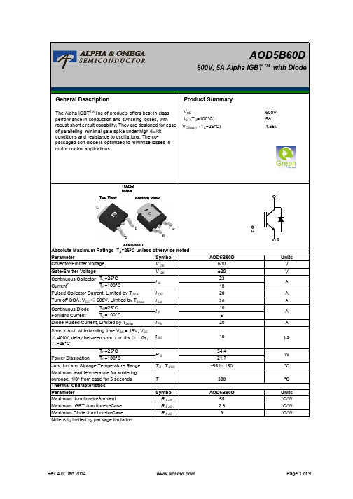
Parasitic Ιnductance=75nH
E off
Turn-Off Energy
E total
Total Switching Energy
t rr Q rr I rm
Diode Reverse Recovery Time
TJ=25°C
Diode Reverse Recovery Charge
Total Switching Energy
Diode Reverse Recovery Time
TJ=150°C
Diode Reverse Recovery Charge
IF=5A,dI/dt=200A/µs,VCE=400V
Diode Peak Reverse Recovery Current
Min Typ Max Units
0 5
8
11
14
17
VGE (V) Fig 6: VGE vs. Short Circuit Time
(VCE=400V,TC=25°C )
30 25 20 15 10 5 0 20
Current(A)
Rev.4.0: Jan 2014
Page 3 of 9
AOD5B60D
-40°C 25°C
150°C
5
0
4
7
10
13
16
VGE(V) Fig 3: Transfer Characteristic
IF (A)
40 35 30 25 20 15 10
5 0
0.0
-40°C 150°C
25°C
0.5
1.0
1.5
2.0
2.5
3.0