MCD26-08IO8B中文资料
Belling BL24C04F 4Kbits (512×8) 电子可编程可读存储器(EEPROM)
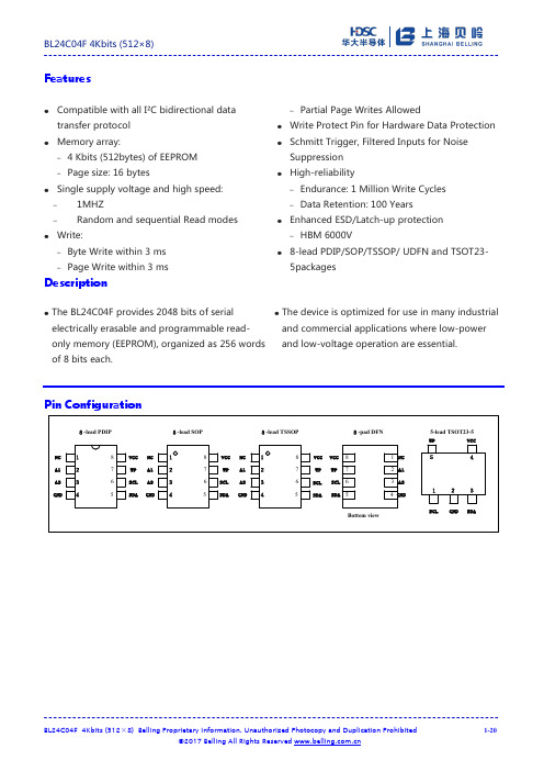
Features●Compatible with all I²C bidirectional datatransfer protocol●Memory array:– 4 Kbits (512bytes) of EEPROM–Page size: 16 bytes●Single supply voltage and high speed:–1MHZ–Random and sequential Read modes ●Write:–Byte Write within 3 ms–Page Write within 3 ms–Partial Page Writes Allowed●Write Protect Pin for Hardware Data Protection ●Schmitt Trigger, Filtered Inputs for NoiseSuppression●High-reliability–Endurance: 1 Million Write Cycles–Data Retention: 100 Years●Enhanced ESD/Latch-up protection–HBM 6000V●8-lead PDIP/SOP/TSSOP/ UDFN and TSOT23-5packagesDescription●The BL24C04F provides 2048 bits of serial electrically erasable and programmable read-only memory (EEPROM), organized as 256 words of 8 bits each. ●The device is optimized for use in many industrial and commercial applications where low-power and low-voltage operation are essential.Pin ConfigurationNC A1 A2 GNDVCCWPNCA1A2GNDNCA1A2GNDNCA1A2GNDVCCWPVCCWPVCCWP123487651234123487658765123487658-lead PDIP8-lead SOP8-lead TSSOP8-pad DFNBottem viewSCLSDASCLSDASCLSDASCLSDAWP VCCSCL SDAGND541235-lead TSOT23-5Pin DescriptionsTable 1Block DiagramFigure 1DEVICE/PAGE ADDRESSES (A2, A1 and A0): The A2, A1 and A0 pins are device address inputs that are hard wire for the BL24C04F. Eight 2K devices may be addressed on a single bus system (device addressing is discussed in detail under the Device Addressing section).SERIAL DATA (SDA): The SDA pin is bi-directional for serial data transfer. This pin is open-drain driven and may be wire-ORed with any number of other open-drain or open- collector devices.SERIAL CLOCK (SCL): The SCL input is used to positive edge clock data into each EEPROM device and negative edge clock data out of each device.WRITE PROTECT (WP):The BL24C04F has a Write Protect pin that provides hardware data protection. The Write Protect pin allows normal read/write operations when connected to ground (GND). When the Write Protection pin is connected to Vcc, the write protection feature is enabled and operates as shown in the following Table 2.Table 2Functional Description1.Memory OrganizationBL24C04F, 4K SERIAL EEPROM: Internally organized with 32 pages of 16 bytes each, the 4K requires a 9-bit data word address for random word addressing.2.Device OperationCLOCK and DATA TRANSITIONS: The SDA pin is normally pulled high with an external device. Data on the SDA pin may change only during SCL low time periods (see Figure 2). Data changes during SCL high periods will indicate a start or stop condition as defined below.START CONDITION: A high-to-low transition of SDA with SCL high is a start condition which must precede any other command (see Figure 3).STOP CONDITION: A low-to-high transition of SDA with SCL high is a stop condition. After a read sequence, the stop command will place the EEPROM in a standby power mode (see Figure 3).ACKNOWLEDGE: All addresses and data words are serially transmitted to and from the EEPROM in 8-bit words. The EEPROM sends a "0" to acknowledge that it has received each word. This happens during the ninth clock cycle.STANDBY MODE: The BL24C04F features a low-power standby mode which is enabled: (a) upon power-up and (b) after the receipt of the STOP bit and the completion of any internal operations.MEMORY RESET: After an interruption in protocol, power loss or system reset, any two-wire part can be reset by following these steps:1. Clock up to 9 cycles.2. Look for SDA high in each cycle while SCL is high.3. Create a start condition.BL24C04F 4Kbits (512×8)BL24C04F 4Kbits (512×8) Belling Proprietary Information. Unauthorized Photocopy and Duplication Prohibited4-20DATA STABLEDATA STABLEDATA CHANGESDASCLFigure 2. Data ValidityFigure 4. Output Acknowledge3.Device AddressingThe 4K EEPROM devices all require an 8-bit device address word following a start condition to enable the chip for a read or write operation (see Figure 5)MSB LSBFigure 5. Device AddressThe device address word consists of a mandatory "1", "0" sequence for the first four most significant bits as shown. This is common to all the Serial EEPROM devices.The 4K EEPROM uses A2 and A1 device address bits to allow as much as for devices on the same bus. These 2 bits must be compared to their corresponding hardwired input pins. The A2 and A1 pins use an internal proprietary circuit that biases them to a logic low condition if the pins are allowed to float.The eighth bit of the device address is the read/write operation select bit. A read operation is initiated if this bit is high and a write operation is initiated if this bit is low.Upon a compare of the device address, the EEPROM will output a "0". If a compare is not made, the chip will return to a standby state.DATA SECURITY: The BL24C04F has a hardware data protection scheme that allows the user to write protect the entire memory when the WP pin is at VCC.4.Write OperationsBYTE WRITE: A write operation requires an 9-bit data word address following the device address word and acknowledgment. Upon receipt of this address, the EEPROM will again respond with a "0" and then clock in the first 8-bit data word. Following receipt of the 8-bit data word, the EEPROM will output a "0" and the addressing device, such as a microcontroller, must terminate the write sequence with a stop condition. At this time the EEPROM enters an internally timed write cycle, tWR, to the nonvolatile memory. All inputs are disabled during this write cycle and the EEPROM will not respond until the write is complete (see Figure 7).MSB LSBFigure 6. ADDRESSSDA LINE STARTDEVICEADDRESSWRITEMSBLSBR/WACKADDRESSACKLSBACKLSBSTOPDATAFigure 7. Byte WritePAGE WRITE: The 4K EEPROM is capable of an 16-byte page write. A page write is initiated the same as a byte write, but the microcontroller does not send a stop condition after the first data word is clocked in. Instead, after the EEPROM acknowledges receipt of the first data word, the microcontroller can transmit up to seven more data words. The EEPROM will respond with a "0" after each data word received. The microcontroller must terminate the page write sequence with a stop condition (see Figure 8).ST A R TDEVICEADDRESSWRITEMSBLSBR/WACKADDRESSACKLSBACKLSBACKSTOPDATA(n)ACKDATA(n+1)DATA(n+1)SDALINEFigure 8. Page WriteThe data word address lower three bits are internally incremented following the receipt of each data word. The higher data word address bits are not incremented, retaining the memory page row location. When the word address, internally generated, reaches the page boundary, the following byte is placed at the beginning of the same page. If more than eight data words are transmitted to the EEPROM, the data word address will "roll over" and previous data will be overwritten.ACKNOWLEDGE POLLING: Once the internally timed write cycle has started and the EEPROM inputs are disabled, acknowledge polling can be initiated. This involves sending a start condition followed by the device address word. The read/write bit is representative of the operation desired. Only if the internal write cycle has completed will the EEPROM respond with a "0", allowing the read or write sequence to continue.5.Read OperationsRead operations are initiated the same way as write operations with the exception that the read/write select bit in the device address word is set to "1". There are three read operations: current address read, random address read and sequential read.CURRENT ADDRESS READ:The internal data word address counter maintains the last address accessed during the last read or write operation, incremented by one. This address stays valid between operations as long as the chip power is maintained. The address "roll over" during read is from the last byte of the last memory page to the first byte of the first page. The address "roll over" during write is from the last byte of the current page to the first byte of the same page. Once the device address with the read/write select bit set to "1" is clocked in and acknowledged by the EEPROM, the current address data word is serially clocked out. The microcontroller does not respond with an input "0" but does generate a following stop condition (see Figure 9).ST A R TDEVICEADDRESSREADMSBLSBR/WACKSTOPDATANOACKSDALINEFigure 9. Current Address ReadRANDOM READ: A random read requires a "dummy" byte write sequence to load in the data word address. Once the device address word and data word address are clocked in and acknowledged by the EEPROM, the microcontroller must generate another start condition. The microcontroller now initiates a current address read by sending a device address with the read/write select bit high. The EEPROM acknowledges the device address and serially clocks out the data word. The microcontroller does not respond with a "0" but does generate a following stop condition (see Figure 10)STA R TDEVICEADDRESSWRITEMSBLSBR/WACKNote.1*=DON'T CARE bitsADDRESSACKLSBSTOPDATA(n)DEVICEADDRESSSTARTREADACKNOACK DUMMY WRITESDALINEFigure 10. Random ReadSEQUENTIAL READ: Sequential reads are initiated by either a current address read or a random address read. After the microcontroller receives a data word, it responds with an acknowledge. As long as theEEPROM receives an acknowledge, it will continue to increment the data word address and serially clock out sequential data words. When the memory address limit is reached, the data word address will "roll over" and the sequential read will continue. The sequential read operation is terminated when the microcontroller does not respond with a "0" but does generate a following stop condition (see Figure 11).DEVICE ADDRESS READR/WACKACKACKACKSTOP DATA(n)DATA(n+1)DATA(n+2)DATA(n+x)NOACKSDALINEFigure 11. Sequential ReadElectrical CharacteristicsAbsolute Maximum Stress Ratings:●DC Supply Voltage . . . . . . . . . . . . . . . . . . . . . . . -0.3V to +6.5V●Input / Output Voltage . . . . . . . . . . . . . GND-0.3V to VCC+0.3V●Operating Ambient Temperature . . . . . . . . . . . . -40℃ to +85℃●Storage Temperature . . . . . . . . . . . . . . . . . . . . .-65℃ to +150℃●Electrostatic pulse (Human Body model) . . . . . . . . . . . . . 6000VComments:Stresses above those listed under "Absolute Maximum Ratings" may cause permanent damage to this device. These are stress ratings only. Functional operation of this device at these or any other conditions above those indicated in the operational sections of this specification is not implied or intended. Exposure to the absolute maximum rating conditions for extended periods may affect device reliability.DC Electrical CharacteristicsApplicable over recommended operating range from: TA = -40℃ to +85℃, VCC = +1.7V to +5.5V (unless otherwise noted)Pin CapacitanceApplicable over recommended operating range from TA = 25℃, f = 1.0 MHz, VCC = +1.7VAC Electrical CharacteristicsApplicable over recommended operating range from TA = -40℃ to +85℃, VCC = +1.8V to +5.5V, CL = 1 TTL Gate and 100 pF (unless otherwise noted)Bus TimingFigure 12. SCL: Serial Clock, SDA: Serial Data I/O Write Cycle TimingFigure 13. SCL: Serial Clock, SDA: Serial Data I/OPackage InformationPDIP Outline Dimensions1.This drawing is for general information only; refer to JEDEC Drawing MS-001, Variation BA for additional information.2. Dimensions A and L are measured with the package seated in JEDEC seating plane Gauge GS-3.3. D, D1 and E1 dimensions do not include mold Flash or protrusions. Mold Flash or protrusions shall not exceed 0.010 inch.4. E and eA measured with the leads constrained to be perpendicular to datum.5. Pointed or rounded lead tips are preferred to ease insertion.6. b2 and b3 maximum dimensions do not include Dambar protrusions. Dambar protrusions shall not exceed 0.010 (0.25 mm).Notes:These drawings are for general information only. Refer to JEDEC Drawing MS-012, Variation AA for proper dimensions, tolerances, datums, etc.1. This drawing is for general information only. Refer to JEDEC Drawing MO-153, Variation AA, for proper dimensions, tolerances, datums, etc.2. Dimension D does not include mold Flash, protrusions or gate burrs. Mold Flash, protrusions and gate burrs shall not exceed 0.15 mm (0.006 in) per side.3. Dimension E1 does not include inter-lead Flash or protrusions. Inter-lead Flash and protrusions shall not exceed 0.25 mm (0.010 in) per side.4. Dimension b does not include Dambar protrusion. Allowable Dambar protrusion shall be 0.08 mm total in excess of the b dimension at maximum material condition. Dambar cannot be located on the lower radius of the foot. Minimum space between protrusion and adjacent lead is 0.07 mm.5. Dimension D and E1 to be determined at Datum Plane H.Figure 17TSOT23-5Figure 18Marking DiagramPDIPBL24C04FYYWW#ZZSSSSSPYY: yearWW :weekZZ: assembly houseSSSSS : Lot IDSOPBL24C04FSSSSSP SSSSS : Lot IDTSSOPBL24C04FSSSSS SSSSS : Lot IDTSOT23-524C04FSSSSSP SSSSS : Lot IDOrdering InformationRevision history。
ADC0808芯片中文资料
典型的集成ADC芯片为了满足多种需要,目前国内外各半导体器件生产厂家设计并生产出了多种多样的ADC 芯片。
仅美国AD公司的ADC产品就有几十个系列、近百种型号之多。
从性能上讲,它们有的精度高、速度快,有的则价格低廉。
从功能上讲,有的不仅具有A/D转换的基本功能,还包括内部放大器和三态输出锁存器;有的甚至还包括多路开关、采样保持器等,已发展为一个单片的小型数据采集系统。
尽管ADC芯片的品种、型号很多,其内部功能强弱、转换速度快慢、转换精度高低有很大差别,但从用户最关心的外特性看,无论哪种芯片,都必不可少地要包括以下四种基本信号引脚端:模拟信号输入端(单极性或双极性);数字量输出端(并行或串行);转换启动信号输入端;转换结束信号输出端。
除此之外,各种不同型号的芯片可能还会有一些其他各不相同的控制信号端。
选用ADC芯片时,除了必须考虑各种技术要求外,通常还需了解芯片以下两方面的特性。
(1)数字输出的方式是否有可控三态输出。
有可控三态输出的ADC芯片允许输出线与微机系统的数据总线直接相连,并在转换结束后利用读数信号RD选通三态门,将转换结果送上总线。
没有可控三态输出(包括内部根本没有输出三态门和虽有三态门、但外部不可控两种情况)的ADC芯片则不允许数据输出线与系统的数据总线直接相连,而必须通过I/O接口与MPU交换信息。
(2)启动转换的控制方式是脉冲控制式还是电平控制式。
对脉冲启动转换的ADC芯片,只要在其启动转换引脚上施加一个宽度符合芯片要求的脉冲信号,就能启动转换并自动完成。
一般能和MPU配套使用的芯片,MPU的I/O写脉冲都能满足ADC芯片对启动脉冲的要求。
对电平启动转换的ADC芯片,在转换过程中启动信号必须保持规定的电平不变,否则,如中途撤消规定的电平,就会停止转换而可能得到错误的结果。
为此,必须用D触发器或可编程并行I/O接口芯片的某一位来锁存这个电平,或用单稳等电路来对启动信号进行定时变换。
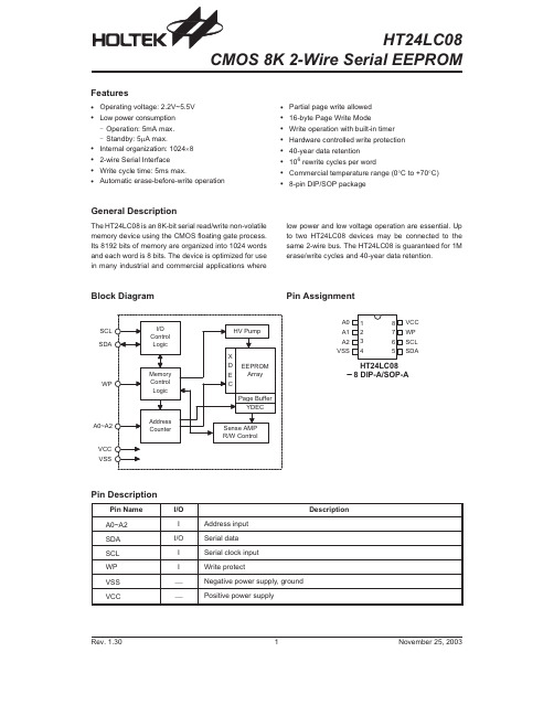
HT24LC08中文资料
D.C. Characteristics
Symbol
Parameter
VCC
Operating Voltage
Test Conditions
VCC
Conditions
¾
¾
ICC1
Operating Current
5V Read at 100kHz
ICC2
Operating Current
5V Write at 100kHz
A0~A2
I
SDA
I/O
SCL
I
WP
I
VSS
¾
VCC
¾
Description Address input Serial data Serial clock input Write protect Negative power supply, ground Positive power supply
Rev. 1.30
¾
¾ 3500 ¾ 900 ns
tBUF
Bus Free Time
Time in which the bus
must be free before a new 4700 ¾ 1200 ¾
ns
transmission can start
tSP
Input Filter Time Constant (SDA and SCL Pins)
¾
¾
100
¾ 400
tHIGH
Clock High Time
¾
4000
¾
600
¾
tLOW
Clock Low Time
¾
4700 ¾ 1200 ¾
tr
ABOV半导体 MC80F0708 0704 MC80F0808 0804 8位单片机 中文手册

A BO V半导体有限公司8位单片机MC80F0708/0704MC80F0808/0804中文手册(1.01版)2008.6ABOV semiconductorwww.abov.co.krMC80F0708/0808修订记录1.01版(6.3.2008)本册修改内部晶振规范1.0版(2.27.2008)在7.4A/D转换特性中增加最小电压参数AV REF。
在7.6典型特征中增加了特性图。
0.5版(9.28.2007)修正8bit计数器说明及图表中的错误。
0.4版(5.5.2007)在1~4MHz,增加操作范围在2.2V~5.5V内。
修正图9-2中的错误:更改R04,R07和PSR1的EC0,EC1为R05,R06和T0O,T2O。
0.3版 (5.2.2007)增加28 QFNP封装。
0.21版(5.2007)增加了T VDD参数规格并且改变了T POR的直流电器特性。
配置选项加入了注释,并对勘误表进行了修正。
0.1版 (8.2006)最初版本1.0版出版发行F A E Tea m©2006A BO V s e m ic ondu c t o r L t d.A ll r ig h t r e s e r v e d.本手册的其它资料由ABOV半导体有限公司韩国办公室或者销售商和代理人提供。
ABOV半导体保留更改数据的权利,并不再另行通知。
这个手册的资料,图表和其它数据都是正确可靠的,但是ABOV半导体没有责任阻止违反专利权或其它权利的个人和团体使用本手册。
注意:本文乃英文版中文翻译,中文文本如有歧义,概以英文为准。
MC80F0708/08081. 概述.............................................................................................................. 描述................................................................................................................. 特性................................................................................................................. 开发工具.......................................................................................................... 订购须知..........................................................................................................2. 系统方框图.....................................................................................................3. 引脚分配.......................................................................................................4. 封装尺寸.......................................................................................................5. 引脚功能.......................................................................................................6. 端口结构.......................................................................................................7. 电器特性.......................................................................................................极限参数.......................................................................................................... 推荐操作参数................................................................................................... A/D转换特性.................................................................................................... DC电器特性.................................................................................................. AC特性............................................................................................................ 典型特性..........................................................................................................8. 存储器结构..................................................................................................... 寄存器.............................................................................................................. 程序存储器........................................................................................................ 数据存储器........................................................................................................ 寻址方式............................................................................................................9. I/O 口............................................................................................................ R0 和R0IO 寄存器........................................................................................... R1 和R1IO 寄存器........................................................................................... R2 和 R2IO 寄存器…………………………………………………………………. R3 和R3IO 寄存器...........................................................................................10. 时钟发生器................................................................................................... 振荡电路..........................................................................................................11. 基本间隔定时器............................................................................................12. 看门狗定时器..............................................................................................13. 定时器/事件计数器....................................................................................... 8位定时/计数器方式....................................................................................... 16位定时/计数器方式...................................................................................... 8位(16位) 比较输出....................................................................................... 8位捕捉方式................................................................................................... 16位捕捉方式.................................................................................................. PWM 方式.........................................................................................................14. 模数转换器...................................................................................................15. 串行输入/输出口(SIO)…………………………………………………………... 发送/接受定时……………………………………………………………………...... 串行I/O的使用………………………………………………………………………..16.蜂鸣器功能…………………………………………………………………………17. 中断............................................................................................................1 1 1 3 4 5 6 7 10 12 16 16 16 16 16 17 18 19 22 22 26 28 33 37 37 40 41 42 42 44 46 49 52 57 58 59 63 66 70 73 74 76 77 79MC80F0708/0808中断优先级 (81)BRK 中断 (83)中断嵌套 (83)外部中断 (85)18. 节电模式操作 (87)Sleep模式 (87)Stop模式 (88)Stop模式(内部RC-振荡看门狗定时器方式) (91)最小消耗电流 (93)19.复位 (95)20.电源失效处理 (97)21.抗干扰措施 (99)振荡噪声保护 (99)振荡失效处理 (100)22.器件配置区 (101)23.仿真器EV A.板安装 (102)A. 指令图 (i)B. 指令集 (ii)MC80F0708/0808 MC80F0708/0704MC80F0808/08041、概述1.1、描述CMOS8位单片机10位A/D转换器MC80F0708(4)/0808(4)是拥有8K(4K)字节FLASH(MTP)程序存储器的CMOS8位单片机。
2008年Ford自动变速箱组件目录说明书

1622008 AUTOMATIC TRANSMISSION KIT & COMPONENTS CATALOG ©2008 PARKER HANNIFIN CORP. ALL RIGHTS RESERVED3790103008397797405R55N / 5R55S / 5R55WRWD 5 SpeedA544510034070670Input ShaftO.Dr. Ring GearO.Dr. CenterShaft783Center SupportInterm. BandDirect DrumForward ClutchForward PlanetReverse BandReverse DrumLow Sprag310037179520036178530311914363912911913910896904896437490996V.B.Parts741E414494765-6370Case313321320Valve Body917747765746322420002OHK Kit004Master L/Steels Kit 006Master 030External Seal Kit1632008 AUTOMATIC TRANSMISSION KIT & COMPONENTS CATALOG ©2008 PARKER HANNIFIN CORP . ALL RIGHTS RESERVEDRWD 5 Speed5R55N / 5R55S / 5R55W862981971961560961971985879565126106146861*229964974877564285872962972104124552894Intermediate Sprag690074266Park Gear264847Park Pawl Assy995-1995-2995-3995916-2916-3919922915916-2916-3919922916263EDA181554770Ext. Hsg.781493305678Output ShaftO.Dr. Band StrutInterm. Band Strut268841Internal Linkage991-2991-3994799991-4761P-4991072410992Yoke1642008 AUTOMATIC TRANSMISSION KIT & COMPONENTS CATALOG©2008 PARKER HANNIFIN CORP. ALL RIGHTS RESERVED*Prefix Letter ‘T’ denotes Toledo-Trans Kit (TTK) Brand Transmission Kits *Prefix Letter ‘B’ denotes Bryco Brand Transmission Kits002.............T16002AP......Overhaul Kit, 5R55N (With Bonded Pistons) 1999-Up ..............................................................1..........002.............T16002GP......Overhaul Kit, 5R55S/5R55W (With Bonded Pistons) 2002-Up..................................................1..........004.............T16004AP......Master L/Steels Kit, 5R55N (With Bonded Pistons) 1999-Up ....................................................1..........004.............T16004GP......Master L/Steels Kit, 5R55S/5R55W (With Bonded Pistons) 2002-Up .......................................1..........006.............T16006AP......Master W/Steels Kit, 5R55N (With Bonded Pistons) 1999-Up...................................................1..........006.............T16006GP......Master W/Steels Kit, 5R55S/5R55W (With Bonded Pistons) 2002-Up ......................................1..........E300...........45019............Gasket, 5R55N Bottom Pan (Plastic With Silicon Bead) OE Style (With Large Holes) 1999-Up 1..........XW4Z-7A191CA D305...........45097668......Gasket, 5R55N/5R55S/5R55W Extension Housing To Case 1999-Up......................................1..........XW4Z-7086-AA A309..........41217............Gasket, 5R55N/5R55S/5R55W Pump Bolt Washer...................................................................AR ........A310..........45097667......Gasket, 5R55N/5R55S/5R55W Pump 1999-Up..........................................................................1..........XW4Z-7A136AB A311...........1988096........O-Ring, 5R55N/5R55S/5R55W Pump Cover 1999-Up ...............................................................1..........XW4Z-7A248AA A313..........1994747........O-Ring, 5R55N Inner Pump Gear 1999-Up.................................................................................1..........F77Z-7L323AA E320...........45097692......Gasket, 5R55N Valve Body Separator Plate To Case 1999-Up ................................................1..........XW4Z-7D100-BF E320...........45097738......Gasket, 5R55S/5R55W Valve Body Separator Plate To Case (Upper) 2002-Up......................1..........1L2Z-7Z490AB-1A070..........70243V..........Seal, 5R55N/5R55S/5R55W Front (No Flange) (Rubber Coated) 1999-Up ..............................1..........F77Z-7A248AA D072...........70083............Seal, 5R55N Linkage 1999-Up ..................................................................................................1..........D5AZ-7B498A D074...........70283............Seal, 5R55N Rear 2WD 2000-Up ...............................................................................................1..........XW4Z-7052AA D074...........70205............Seal, 5R55S/5R55W Rear (W/Long Boot) 2WD 2002-Up .........................................................1..........F6UZ-7052A D074...........70282............Seal, 5R55S/5R55W Extension Housing 4X4 2002-Up .............................................................1..........1L2Z-7052BA175.............6358..............Ring Kit, 5R55N/5R55S/5R55W (2 Metal 4PTFE 2 Torlon Rings) 1999-Up ...............................1..........A178..........45060279......Ring, 5R55N, 5R55W, 5R55S Pump Support (Lock-Up) 1999-Up .............................................1..........B181...........TAW- 2212....Ring, 5R55N, 5R55W, 5R55S Forward Clutch Cylinder 1999-Up .............................................2..........D184...........45060265......Ring, 5R55N, 5R55W, 5R55S Output Shaft 1999-Up.................................................................1..........A179..........30308............Ring, 5R55N, 5R55W, 5R55S Overdrive Brake Drum 1999-Up.................................................2..........B179...........30308P ..........Ring, 5R55N, 5R55W, 5R55S Direct Clutch (Center Support) 1999-Up Torlon .........................2..........119.............45082NR........Friction Module, 5R55N 1999-Up................................................................................................1..........119.............45082LR........Friction Module, 5R55S/5R55W 2002-Up...................................................................................1..........E010...........45040N ..........Filter, 5R55N (3/8” Tall Pick-up Tube) 1999-Up ..........................................................................1..........XW4Z-7A098BB E010...........F-340.............Filter, 5R55S/5R55W (2 1/4” Tall Pick-Up Tube) 2002-Up..........................................................1..........1L2Z-7A098AC5R55N / 5R55S / 5R55WRWD 5 Speed1652008 AUTOMATIC TRANSMISSION KIT & COMPONENTS CATALOG ©2008 PARKER HANNIFIN CORP. ALL RIGHTS RESERVEDB022...........45090............Band, 5R55N Overdrive/Intermediate (Hi-Energy) 1999-Up......................................................2..........XW4Z-7D034BA 030.............45030G..........Bushing Kit, 5R55N/5R55S/5R55W 1999-Up.............................................................................1..........A034..........31530............Bushing, 5R55N/5R55S/5R55W Pump Cover 1999-Up .............................................................1..........A036..........31531............Bushing, 5R55N/5R55S/5R55W Overdrive Sun Gear 1999-Up................................................1..........A036..........45039............Bushing, 5R55N/5R55S/5R55W Stator (Front) 1999-Up ...........................................................1..........A037..........31532............Bushing, 5R55N/5R55S/5R55W Stator (Rear) 1999-Up............................................................1..........A046..........31533............Bushing, 5R55N/5R55S/5R55W Coast Clutch Drum e 56036A................................................................................................................................1..........B211...........45176A..........Washer, 5R55N/5R55S/5R55W Pump To Coast Clutch Drum .063" (Plastic) 1999-Up.............1..........F7TZ-7D014TA B211...........45176B ..........Washer, 5R55N/5R55S/5R55W Pump To Coast Clutch Drum .071" (Plastic) 1999-Up.............1..........F7TZ-7D014MA B211...........45176C ..........Washer, 5R55N/5R55S/5R55W Pump To Coast Clutch Drum .075" (Plastic) 1999-Up.............1..........F7TZ-7D014NA B211...........45176D ..........Washer, 5R55N/5R55S/5R55W Pump To Coast Clutch Drum .079" (Plastic) 1999-Up.............1..........F7TZ-7D014PA B211...........45176E ..........Washer, 5R55N/5R55S/5R55W Pump To Coast Clutch Drum .083" (Plastic) 1999-Up.............1..........F7TZ-7D014RA B211...........45176F ..........Washer, 5R55N/5R55S/5R55W Pump To Coast Clutch Drum .087" (Plastic) 1999-Up.............1..........F7TZ-7D014SA C232...........45145............Washer, 5R55N/5R55S/5R55W Bearing to Forward Hub (Solid Bronze) 1999-Up .................1..........FOTZ-7D090A D263...........45077............Washer, 5R55N/5R55S/5R55W Parking Gear To Case 1999-Up ..............................................1..........D4ZZ-7B368-AD410...........D56955J ........Switch, 5R55N Neutral Safety (12 Prong Connector) 1999-Up ...............................................1..........XW4Z-7F293AA E922...........33991............Nut, 5R55N/S/W Band 1999-Up .................................................................................................2..........380850-SRWD 5 Speed5R55N / 5R55S / 5R55W。
ICL8038_中文资料
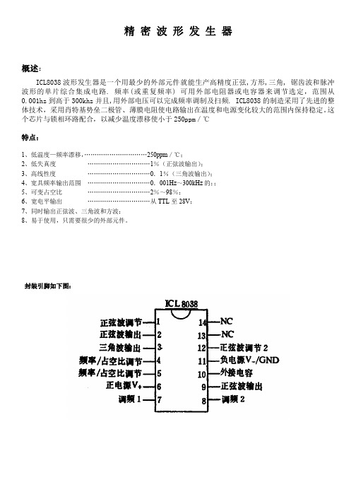
精密波形发生器概述:ICL8038波形发生器是一个用最少的外部元件就能生产高精度正弦,方形,三角,锯齿波和脉冲波形的单片综合集成电路.频率(或重复频率)可用外部电阻器或电容器来调节选定,范围从0.001hz到高于300khz并且,用外部电压可以完成频率调制及扫频.ICL8038的制造采用了先进的整体技术,采用肖特基势垒二极管、薄膜电阻使电路输出在温度和电源变化较大的范围内保持稳定。
这个芯片与锁相环路配合,以减少温度漂移使小于250ppm/℃特点:1、低温度—频率漂移,…………………………250ppm/℃;2、低失真度…………………………1%(正弦波输出);3、高线性度…………………………0.1%(三角波输出);4、宽具频率输出范围…………………………0.001Hz~300kHz的;;5、可变占空比…………………………2%~98%;6、宽电平输出…………………………从TTL至28V;7、同时输出正弦波、三角波和方波;8、易于使用,只需要很少的外部元件。
封装引脚如下图:ICL8038内部原理框图最大限值范围:供电电压(V-to V+) (36V)到V+输入电压(任何管脚) (V)–输入电流(管4-5).......................................25mA输出槽电流(管脚3和9)..................................25mA工作条件温度范围ICL8038AC,ICL8038BC,ICL8038CC............0℃to70℃图1:测试电路图2ICL8038内部详细的示意图应用信息(看功能图)由两个恒流源对外接电容C进行充电和放电,恒流源2的工作状态由触发器控制,同时恒流源1始终打开。
假设,触发器使得恒流源2关闭电容C由恒流源1充电,电容器C两端电压随时间线性上升。
当这个电压达到比较器1的输入电平(设定在2/3电源电压),触发器翻转改变状态,使恒流源2处于关闭状态。
MCX08M2电子控制器说明书

MCX08M2 is an electronic controller that holds all the typical functionalities of MCX controllers in the compact size of 8 DIN modules:•Programmability•Connection to the CANbus local network •Modbus RS485 opto-insulated serial interface It is available in the version with or without graphic LCD display, and 110 / 230 V AC or 24 V AC power supply.Features:•8 analog and 8 digital inputs •4 analog and 8 digital outputs•Power supply 24 V AC / 20 / 60 V DC and 110V / 230 V AC•Remote access to data through CANbus connection for additional display (LCD available) and keyboard•RTC clock for managing weekly time programs and data logging information•Modbus RS485 opto-insulated serial interface •Dimensions 8 DIN modules•Available with graphic LCD display and without display for showing the desiredinformation24 V or24 V or24 V orGeneral featuresInput/OutputConnection diagram Top boardBottom boardNOTE:*Connection has to be made on the first and last local network units, make the connection as close as possible to the connector.**Optoinsulated analog outputs voltages are referenced to contact N1.ConnectionDimensionsProduct part numbers(1)080G0314 is available in Industrial Pack only. The corresponding Single Pack version is 080G0317 but cannot be ordered singularly.Accessories part numbersNOTE:Single Pack codes include standard connectors kit, Industrial Pack code don’t include standard connectors kit.Certificates, declarations, and approvalsThe list contains all certificates, declarations, and approvals for this product type. Individual code number may have some or all of these approvals, and certain local approvals may not appear on the list.Some approvals may change over time. You can check the most current status at or contact your local Danfoss representative if you have any questions.Danfoss can accept no responsibility for possible errors in catalogues, brochures and other printed material. Danfoss reserves the right to alter its products without notice. This also applies to products already on order provided that such alterations can be made without subsequentialchanges being necessary in specifications already agreed. All trademarks in this material are property of the respective companies. Danfoss and the Danfoss logotype are trademarks of Danfoss A/S. All rights reserved.Online supportDanfoss offers a wide range of support along with our products, including digital product information, software,mobile apps, and expert guidance. See the possibilities below.The Danfoss Product StoreThe Danfoss Product Store is your one-stop shop for everything product related—no matter where you are in the world or what area of the cooling industry you work in. Get quick access to essential information like product specs, code numbers, technical documentation, certifications, accessories,and more.Start browsing at .Find technical documentationFind the technical documentation you need to get your project up and running. Get direct access to our official collection of data sheets, certificates and declarations, manuals and guides, 3D models and drawings, case stories, brochures, and much more.Start searching now at /en/service-and-support/documentation .Danfoss LearningDanfoss Learning is a free online learning platform. It features courses and materials specifically designed to help engineers, installers, service technicians, and wholesalers better understand the products, applications, industry topics, and trends that will help you do your job better.Create your Danfoss Learning account for free at /en/service-and-support/learning .Get local information and supportLocal Danfoss websites are the main sources for help and information about our company andproducts. Find product availability, get the latest regional news, or connect with a nearby expert—all in your own language.Find your local Danfoss website here: /en/choose-region .。
ADC0809中文资料

A D C0809中文资料(总5页) -CAL-FENGHAI.-(YICAI)-Company One1-CAL-本页仅作为文档封面,使用请直接删除ADC0809是带有8位A/D转换器、8路多路开关以及微处理机兼容的控制逻辑的CMOS组件。
它是逐次逼近式A/D转换器,可以和单片机直接接口。
(1)ADC0809的内部逻辑结构由下图可知,ADC0809由一个8路模拟开关、一个地址锁存与译码器、一个A/D转换器和一个三态输出锁存器组成。
多路开关可选通8个模拟通道,允许8路模拟量分时输入,共用A/D转换器进行转换。
三态输出锁器用于锁存A/D转换完的数字量,当OE端为高电平时,才可以从三态输出锁存器取走转换完的数据。
(2).ADC0809引脚结构ADC0809各脚功能如下:D7-D0:8位数字量输出引脚。
IN0-IN7:8位模拟量输入引脚。
VCC:+5V工作电压。
GND:地。
REF(+):参考电压正端。
REF(-):参考电压负端。
START:A/D转换启动信号输入端。
ALE:地址锁存允许信号输入端。
(以上两种信号用于启动A/D转换)EOC:转换结束信号输出引脚,开始转换时为低电平,当转换结束时为高电平。
OE:输出允许控制端,用以打开三态数据输出锁存器。
CLK:时钟信号输入端(一般为500KHz)。
A、B、C:地址输入线。
ADC0809对输入模拟量要求:信号单极性,电压范围是0-5V,若信号太小,必须进行放大;输入的模拟量在转换过程中应该保持不变,如若模拟量变化太快,则需在输入前增加采样保持电路。
地址输入和控制线:4条ALE为地址锁存允许输入线,高电平有效。
当ALE线为高电平时,地址锁存与译码器将A,B,C三条地址线的地址信号进行锁存,经译码后被选中的通道的模拟量进入转换器进行转换。
A,B和C为地址输入线,用于选通IN0-IN7上的一路模拟量输入。
通道选择表如下表所示。
C B A选择的通道000IN0001IN1010IN2011IN3100IN4101IN5110IN6数字量输出及控制线:11条ST为转换启动信号。
巴鲁夫 工业 RFID系统 产品手册说明书

Industrial RFID systems MANAGING ALL YOUR DATABalluff offers you a wide selection of data carriers and read/write heads for LF, HF and UHF applications. With the BIS V multi-frequency processor unit, all systems can be combined with each other. This adds flexibility and saves costs through lower inventory levels.Industrial RFID systems – managing all your dataAutomatic identification and tracking in productionTHE PERFORMANCE RANGEYour Balluff solutionsn HF RFID system (13.56 MHz) BIS M n LF RFID system (70/455 kHz) BIS C n LF RFID system (125 kHz) BIS L n UHF RFID system (860/960 MHz) BIS UGo online to individually configure your own system www.balluff.de/go/rfid-configuratorIO-LINK ALL-IN-ONE BIS V PROCESSOR UNIT1 Network block2 Read/write heads with IO-Link3 Data carriers4 Read/write heads with integrated processor unit5 Universal processor unit6 Read/write heads2266433315UHF by country-specific frequencies1 South Korea LF: 125 kHz HF: 13.56 MHzUHF: 917...920.8 MHz 2 JapanLF: 125 kHz HF: 13.56 MHzUHF: 916.7...920.8 MHz 3 ChinaLF: 125 kHz HF: 13.56 MHzUHF: 840.5...844.5 MHz 4 AustraliaLF: 125 kHz HF: 13.56 MHz UHF: 920...926 MHz5 South Africa LF: 125 kHz HF: 13.56 MHzUHF: 865.6...867.6 MHz 6 EuropeLF: 125 kHz HF: 13.56 MHzUHF: 865.6...867.6 MHz 7 USA/Canada/Mexico LF: 125 kHz HF: 13.56 MHz UHF: 902...928 MHz 8 BrazilLF: 125 kHz HF: 13.56 MHzUHF: 902...907.5 MHzWHAT ARE THECONSEQUENCES OF THE DIFFERENT FREQUENCIES?Briefly stated, different frequencies mean different working ranges, since the frequency determines the range. The frequency also affects the coupling behavior (see: How the system components communicate).LF is best suited for close range and for difficult conditions such as metallic surroundings. LF is therefore often used in tool identification.HF is ideal for parts tracking at close range up to 400 mm. With HF you can process and store larger quantities of data at high transmission speeds.UHF typically communicates at a range of 6 m distance. UHF allows simultaneous reading of multiple data carriers (multi-tagging).System frequenciesWorking range of the Balluff BIS RFID systemsSYSTEM STRUCTURERFID requires three main components. These form an RFID system:–■Data carrier (data storage)–■Read/write head (data transmission)–■Processor unit (data processing and communication)The system components in detail–■Data carrier (Tag/Data Carrier)Stores all kinds of data which is read or written by computers or automation equipment. The data carrier antenna sends and receives the signals. Read/write versions are available in various memory capacities and with various storage mechanisms.– Passive data carriers: without power supply – Active data carriers: with power supply–■Read/write headProvides power to the data carrier, reads its data and writes new data to it. It sends this data to the processor unit where the data is further processed. –■AntennaTransmits the power.– HF-/LF systems: Antenna is integrated in the read/write head– UHF systems: Usually passive antennas without read/write head electronics (integrated into the processor unit).–■Processor unitUsed for signal processing and preparation. It typically includes an integrated interface for connecting to the controller/PC system.UHF system: The read/write function can be integrated into the processor unit, so that only a passive antenna and the data carrier are required.How the system components communicateThe data carrier and read/write head connect via the frequency-dependent coupling.With UHF the coupling is via electromagnetic waves, and for LF and HF the coupling is inductive.Components of a HF/LF systemData carrier Read/write head Processor unitUsed at close range, the data carrier must be placed exactly within the read range of the read/write head.Components of a UHF systemData carrier Antenna withProcessor unitread/write head electronicsData carrier Passive antennaProcessor unit withread/write head electronicsIn UHF systems close placement of the data carrier in front of the antenna is not necessary because of the large working range. Still, there are a few rules (see: What to know about UHF systems).Various industry standards are in place both for theLF/HF range and for UHF for communication between the system components. These specify how the information is transmitted. There are also proprietary manufacturer-specific solutions available (see: What you need to know about LF/HF systems/UHF systems).SYSTEM CHARACTERISTICSWhy data storage is importantSelection of the data storage determines where data can be processed and with which components. You can use either of two storage concepts: the central database and decentralized data retention.Central data storage–■All data records are stored in a central database –■Data carrier is simply an identifier –■Mainly for reading informationCan be LF, HF or UHF systems, but mainly used with UHF systemsDecentralized data retention–■All data records are stored on data carriers –■The data carrier stores the identifier and all data records (no central database)–■For both reading and writing informationMainly used with HF/LF systemsWHAT YOU NEED TO KNOW ABOUT LF/HF SYSTEMSIn brief, the read/write distance in LF/HF systems is affected by the antenna shape and the traverse speed.When installing the data carriers the installation conditions and close proximity of metal play a role.Antenna shapeData carriers and read/write heads are constructedwith a rod or round antenna. To achieve the best results the antenna shape must be identical to that of the read/write head. This means: Use rod antenna with rod antenna or round antenna with round antenna.The antenna shape determines different field distributions and read distances. It also determines the active communication field.Ideal working rangeRound antenna–■The lobe of the antenna field is distributed evenly and symmetrically–■No polarization or directionality, even offset.This means the data carrier and read/write head Rod antenna–■The lobe of the antenna field is distributed unevenly and has additional sidelobes–■The is polarization and directionality, which allows greater read distances than with a round antenna–■Identical orientation of the data carrier and read/write head is important in order to achieve greater read distancesInstalling data carriersAccount for distance to metalTo reach the specified read/write distance, a data carrier in a metallic environment must be mounted at a certain distance from metal and within a certain metal-free clear zone. The exact specifications can be found in the data sheets. The following distinctions are made:–■Flush in metalThe sensing surface can be mounted flush on the surface of steel so that it is even with adjacent areas. The range here is less than for differently constructed/installed data carriers of the same size.–■On metalThe sensing surface must not be in contact or surrounded by steel.–■Metal-free (clear zone)The entire area of the data carrier must be kept clear of any type of metal.12365874Data carriers with various memory types are available Traditional memory chips are EEPROM and FRAM.Both types use inductive coupling for power supply and data transmission. They differ in the maximum number of write cycles.–■EEPROM (Electrical erasable programmableread only memory): 100,000 to 1,000,000 write cycles –■FRAM (Ferro-electrical random access memory): 1010 write cyclesHow traverse speed, read/write distance and data transmission time relate to each otherFor reliable data transfer between read/write head andDynamic read/write modeThe data carrier passes by the read/write head without stopping. This should be as close as possible to achieve a long read/write path.How to calculate the traverse speed for dynamic applications Traverse speed (v)Offset (s)=At least 315 mm of offset is required to read the data within a dwell time of 45 ms. Assuming the maximum offset is 340 mm, the read distance must be configured to be very short. The greater the offset of the read/write head, the greater the distance between data carrier and read/write head can be.Important industry standards–■ISO 15693International series of standards for non-contacting chip cards, identification systems and access controls. Operates at a frequency of 13.56 MHz and is the prevailing standard in automation.ISO 15693 defines the protocols for communication between data carrier and read/write head. The datacarriers and read/write heads from different suppliers are generally compatible if they adhere to the same standard. –■ISO 14443International series of standards for non-contact chipcards. These are used in identification systems and access controlling, but also for payment applications such as credit cards, public transportation tickets, etc. Operates at a frequency of 13.56 MHz.In contrast to the ISO 15693 standard, ISO 14443specifies that the data carrier and read/write head carry a manufacturer-specific identifier. Only if the identifiers agree can they communicate with each other.Balluff uses the most commonly accepted contactless chip technology NXP Mifare. This complies with ISO-Standards ISO 7816 and ISO 14443A.High performance solutions from BalluffIn addition to the industry standards there are proprietary systems that are not described by any standard. For example, high-performance solutions from Balluff that are faster and process more data than these industry standards allow. Here the following components are used:–■High-memory data carriers: Data carriers with a memory capacity > 8 kilobytes.–■High-speed data carriers: Combined with the associated read/write heads you can achieve up to eight times greater read speeds than applications that fall under DIN ISO 15693.WHAT YOU NEED TO KNOW ABOUT UHF SYSTEMSPower transmission between data carrier and read/write head is essential for optimal function of a UHF RFID system. Whether and how the antennas need to be aligned with each other depends on the type of polarization of the antennas.Relationship between antenna polarization and data carrier orientationThe polarization of a UHF antenna is determined by the direction of the electrical field of the wave.–■Linear polarized antennasThe electrical field runs either vertical or horizontal to be identically aligned in order to transmit power.–■Data carrier antennaIn UHF systems the coupling is electromagnetic. To transmit data the data carrier‘s antenna converts electromagnetic waves and high-frequency alternating current into each other. Here the polarization direction of the sending antenna and the orientation of the data carrier must be selected correctly. (See illustration for how to achieve optimal power transmission).Construction of a UHF data carrierUHF data carriers with a dipole antenna are often selected (see illustration above). Many other antenna shapes are available as well. These offer particular properties and determine the form factor of the data carrier.Other form factors for UHF data carriersTypical UHF industry standards–■ISO/IEC 18000-6:2013International series of standards that provide the general description of the air interface and signal transmission. The latest standard ISO 18000-63 was published in 2015.–■EPC Class1 Gen2Was published by the standardization organization EPC global, which develops voluntary standards. EPC Class 1 Gen2 Version 2.0.1 is fully compatible with ISO 18000-63.This compatibility mans you can use the same hardware infrastructure and the same data carriers both in an ISO standard environment and an EPC environment.Both standards are suitable for worldwide use. You must however take note of the various national RF regulations.UHF antenna field requires specific test scenariosIn brief: Since the surroundings affect the antenna field, you must perform the closest possible simulation of the ambient conditions.The UHF antenna beams its signal in a wide opening angle. Undesired reflections and absorption in a UHF RFID system Typical ideal antenna fieldin overlapping of wavetrains. Overall it can result in local fields with higher and lower field strengths, or even field collapses (read holes).If a data carrier finds itself in such a read hole, it can no longer communicate with the read/write head.Headquarters Balluff GmbHSchurwaldstrasse 973765 Neuhausen a. d. F.GermanyPhone +49 7158 173-0Fax +49 7158 5010******************D o c . n o . 949747E N · I 20 · S u b j e c t t o c h a n g e s .CONTACT OUR WORLDWIDE SUBSIDIARIES。
ICL8038CCPD中文资料

NOTE: Add /883B to part number if 883 processing is required.
Pinout
ICL8038 (PDIP, CERDIP) TOP VIEW
Functional Diagram
V+ CURRENT SOURCE #1 I 14 NC 2I 13 NC 12 SINE WAVE ADJUST 11 V- OR GND 10 TIMING CAPACITOR 9 8 SQUARE WAVE OUT FM SWEEP INPUT BUFFER BUFFER CURRENT SOURCE #2 FLIP-FLOP V- OR GND 11 SINE CONVERTER C COMPARATOR #2 10 6 COMPARATOR #1
Ordering Information
PART NUMBER ICL8038CCPD ICL8038CCJD ICL8038BCJD ICL8038ACJD ICL8038BMJD (Note) ICL8038AMJD (Note) STABILITY 250ppm/oC (Typ) 250ppm/oC (Typ) 180ppm/oC (Typ) 120ppm/oC (Typ) 350ppm/oC (Max) 250ppm/oC (Max) TEMP. RANGE (oC) 0 to 70 0 to 70 0 to 70 0 to 70 -55 to 125 -55 to 125 PACKAGE 14 Ld PDIP 14 Ld CERDIP 14 Ld CERDIP 14 Ld CERDIP 14 Ld CERDIP 14 Ld CERDIP PKG. NO. E14.3 F14.3 F14.3 F14.3 F14.3 F14.3
SA8026中文资料
元器件交易网0.250.50.751 1.251.51.752 2.252.52.75COMPLIANCE VOLTAGE (V)Figure 12.PHI Charge Pump Output vs. Temperature (CP = 00; V DD = 3.0 V; I SET = 165.33 m A)TSSOP20:plastic thin shrink small outline package; 20 leads; body width 4.4 mm SOT360-1DefinitionsShort-form specification — The data in a short-form specification is extracted from a full data sheet with the same type number and title. For detailed information see the relevant data sheet or data handbook.Limiting values definition — Limiting values given are in accordance with the Absolute Maximum Rating System (IEC 134). Stress above one or more of the limiting values may cause permanent damage to the device. These are stress ratings only and operation of the device at these or at any other conditions above those given in the Characteristics sections of the specification is not implied. Exposure to limiting values for extended periods may affect device reliability.Application information — Applications that are described herein for any of these products are for illustrative purposes only. Philips Semiconductors make no representation or warranty that such applications will be suitable for the specified use without further testing or modification.DisclaimersLife support — These products are not designed for use in life support appliances, devices or systems where malfunction of these products can reasonably be expected to result in personal injury. Philips Semiconductors customers using or selling these products for use in such applications do so at their own risk and agree to fully indemnify Philips Semiconductors for any damages resulting from such application.Right to make changes — Philips Semiconductors reserves the right to make changes, without notice, in the products, including circuits, standard cells, and/or software, described or contained herein in order to improve design and/or performance. Philips Semiconductors assumes no responsibility or liability for the use of any of these products, conveys no license or title under any patent, copyright, or mask work right to these products, and makes no representations or warranties that these products are free from patent, copyright, or mask work right infringement, unless otherwise specified.Philips Semiconductors811 East Arques AvenueP.O. Box 3409Sunnyvale, California 94088–3409Telephone 800-234-7381© Copyright Philips Electronics North America Corporation 1999All rights reserved. Printed in U.S.A.Date of release: 11-99。
AT24C512B_08中文资料
AT24C512B_08中文资料FeaturesLow-voltage and Standard-voltage Operation–1.8v (V CC = 1.8V to 3.6V)–2.5v (V CC = 2.5V to 5.5V)?Internally Organized 65,536 x 8?Two-wire Serial InterfaceSchmitt Triggers, Filtered Inputs for Noise Suppression ?Bidirectional Data Transfer Protocol1 MHz (2.5V , 5.5V), 400 kHz (1.8V) CompatibilityWrite Protect Pin for Hardware and Software Data Protection ?128-byte Page Write Mode (Partial Page Writes Allowed)?Self-timed Write Cycle (5 ms Max)?High Reliability–Endurance: 1,000,000 Write Cycles –Data Retention: 40 Years ?Lead-free/Halogen-free Devices8-lead PDIP , 8-lead JEDEC SOIC, 8-lead EIAJ SOIC, 8-lead TSSOP , 8-ball dBGA2, and 8-lead Ultra Thin Small Array (SAP) PackagesDie Sales: Wafer Form, Waffle Pack and Bumped DieDescriptionThe AT24C512B provides 524,288 bits of serial electrically erasable and programma-ble read only memory (EEPROM) organized as 65,536 words of 8 bits each. The device’s cascadable feature allows up to eight devices to share a common two-wire bus. The device is optimized for use in many industrial and commercial applications where low-power and low-voltage operation are essential. The devices are available in space-saving 8-pin PDIP, 8-lead JEDEC SOIC, 8-lead EIAJ SOIC, 8-lead TSSOP,8-ball dBGA2 and 8-lead Ultra Thin SAP packages. In addition, the entire family is available in 1.8V (1.8V to 3.6V) and 2.5V (2.5V to 5.5V) versions.T able 0-1.Pin ConfigurationsPin Name Function A0–A2Address Inputs SDA Serial Data SCL Serial Clock Input WPWrite ProtectRev. 5297A–SEEPR–1/08Two-wire Serial EEPROM512K (65,536 x 8)AT24C512Bwith Three Device Address Inputs8-lead PDIP8-lead TSSOPBottom View8-lead SOIC8-ball dBGA2Bottom View25297A–SEEPR–1/08AT24C512BFigure 0-1.Block Diagram Absolute Maximum Ratings*Operating T emperature..................................–55°C to +125°C *NOTICE:Stresses beyond those listed under “Absolute Maximum Ratings” may cause permanent dam-age to the device. This is a stress rating only and functional operation of the device at these or any other conditions beyond those indicated in the operational sections of this specification is not implied. Exposure to absolute maximum rating conditions for extended periods may affect device reliability.Storage T emperature.....................................–65°C to +150°C Voltage on Any Pinwith Respect to Ground....................................–1.0V to +7.0V Maximum Operating Voltage ..........................................6.25V DC Output Current........................................................5.0 mA35297A–SEEPR–1/08AT24C512B1.Pin DescriptionSERIAL CLOCK (SCL): The SCL input is used to positive edge clock data into each EEPROM device and negative edge clock data out of each device.SERIAL DATA (SDA): The SDA pin is bidirectional for serial data transfer. This pin is open-drain driven and may be wire-ORed with any number of other open-drain or open collector devices.DEVICE/PAGE ADDRESSES (A2, A1, A0): The A2, A1, and A0 pins are device address inputs that are hardwired (directly toGND or to Vcc) for compatibility with other AT24Cxx devices.When the pins are hardwired, as many as eight 512K devices may be addressed on a single bus system. (Device addressing is discussed in detail under “Device Addressing,” page 8.) A device is selected when a corresponding hardware and software match is true. If these pins are left floating, the A2, A1, and A0 pins will be internally pulled down to GND. However, due to capaci-tive coupling that may appear during customer applications, Atmel ? recommends always connecting the address pins to a known state. When using a pull-up resistor, Atmel recommends using 10k Ω or less.WRITE PROTECT (WP): The write protect input, when connected to GND, allows normal write operations. When WP is connected directly to Vcc, all write operations to the memory are inhib-ited. If the pin is left floating, the WP pin will be internally pulled down to GND. However, due to capacitive coupling that may appear during customer applications, Atmel recommends always connecting the WP pins to a known state. When using a pull-up resistor, Atmel rec ommends using 10k Ω or less.45297A–SEEPR–1/08AT24C512B2.Memory OrganizationAT24C512B, 512K SERIAL EEPROM: The 512K is internally organized as 512 pages of 128-bytes each. Random word addressing requires a 16-bit data word address.Note:1.This parameter is characterized and is not 100% tested.Note:1.V IL min and V IH max are reference only and are not tested.Table 2-1.Pin Capacitance (1)Applicable over recommended operating range from: T A = 25°C, f = 1.0 MHz, V CC = +1.8V to +5.5VSymbol Test ConditionMax Units Conditions C I/O Input/Output Capacitance (SDA)8pF V I/O = 0V C IN Input Capacitance (A 0, A 1, SCL) 6pFV IN = 0VTable 2-2.DC CharacteristicsApplicable over recommended operating range from: T AI = –40°C to +85°C, V CC = +1.8V to +5.5V (unless otherwise noted) Symbol Parameter Test ConditionMin TypMax Units V CC1Supply Voltage 1.8 3.6V V CC2Supply Voltage 2.55.5V I CC Supply Current V CC = 5.0V READ at 400 kHz 2.0mAI CC Supply Current V CC = 5.0V WRITE at 400 kHz 3.0mA I SB1Standby CurrentV CC = 1.8V V IN = V CC or V SS1.0μA V CC = 3.6V 3.0μA I SB2Standby Current V CC =2.5V V IN = V CC or V SS2.0μA V CC = 5.5V 6.0μA I LI Input Leakage Current V IN = V CC or V SS 0.10 3.0μA I LO Output Leakage CurrentV OUT = V CC or V SS0.053.0μA V IL Input Low Level (1)–0.6V CC x 0.3V V IH Input High Level (1)V CC x 0.7V CC + 0.5V V OL1Output Low Level V CC = 1.8V I OL = 0.15 mA 0.2V V OL2Output Low LevelV CC = 3.0VI OL = 2.1 mA 0.4V55297A–SEEPR–1/08AT24C512BNotes:1.This parameter is ensured by characterization only.2.AC measurement conditions:R L (connects to V CC ): 1.3 k Ω (2.5V , 5V), 10 k Ω (1.8V)Input pulse voltages: 0.3 V CC to 0.7 V CC Input rise and fall times: ≤ 50 nsInput and output timing reference voltages: 0.5 V CCTable 2-3.AC Characteristics (Industrial Temperature)Applicable over recommended operating range from T AI = ?40°C to +85°C, V CC = +1.8V to +5.5V, CL = 100 pF (unless oth-erwise noted). Test conditions are listed in Note 2.Symbol Parameter1.8-volt2.5, 5.0-volt Units MinMax MinMax f SCL Clock Frequency, SCL 4001000kHz t LOW Clock Pulse Width Low 1.30.4μs t HIGH Clock Pulse Width High 0.60.4μs t i Noise Suppression Time (1)10050ns t AA Clock Low toData Out Valid 0.050.90.050.55μs t BUF Time the bus must be free before a new transmission can start (1) 1.30.5μs t HD.ST A Start Hold Time 0.60.25μs t SU.ST A Start Set-up Time 0.60.25μs t HD.DA T Data In Hold Time 00μs t SU.DAT Data In Set-up Time 100 100ns t R Inputs Rise Time (1)0.30.3μs t F Inputs Fall Time (1)300 100ns t SU.STO Stop Set-up Time 0.60.25μs t DH Data Out Hold Time 5050ns t WRWrite Cycle Time 55ms Endurance (1)25°C, Page Mode, 3.3V1,000,000Write Cycles65297A–SEEPR–1/08AT24C512B3.Device OperationCLOCK and DATA TRANSITIONS: The SDA pin is normally pulled high with an external device.Data on the SDA pin may change only during SCL low time periods (see Figure 3-4 on page 8).Data changes during SCL high periods will indicate a start or stop condition as defined below.START CONDITION: A high-to-low transition of SDA with SCL high is a start condition which must precede any other command (see Figure 3-5 on page 8).STOP CONDITION: A low-to-high transition of SDA with SCLhigh is a stop condition. After a read sequence, the stop command will place the EEPROM in a standby power mode (see Fig-ure 3-5 on page 8).ACKNOWLEDGE: All addresses and data words are serially transmitted to and from the EEPROM in 8-bit words. The EEPROM sends a zero during the ninth clock cycle to acknowl-edge that it has received each word.STANDBY MODE: The AT24C512B features a low power standby mode which is enabled: a)upon power-up and b) after the receipt of the STOP bit and the completion of any internal operations.Software Reset: After an interruption in protocol, power loss or system reset, any 2-wire part can be protocol reset by following these steps: (a) Create a start bit condition, (b)clock 9 cycles, (c) create another start bit followed by stop bit condition as shown below.The device is ready for next communication after above steps have been completed.Figure 3-1.Protocol Reset Condition75297A–SEEPR–1/08AT24C512BFigure 3-3.Write Cycle Timing (SCL: Serial Clock, SDA: Serial Data I/O)Note:1.The write cycle time t WRis the time from a valid stop condition of a write sequence to the end of the internal clear/write cycle.85297A–SEEPR–1/08AT24C512BFigure 3-4.Data ValidityFigure 3-5.Start and Stop DefinitionFigure 3-6.Output Acknowledge95297A–SEEPR–1/08AT24C512B4.Device AddressingThe 512K EEPROM requires an 8-bit device address word following a start condition to enable the chip for a read or write operation (see Figure 6-1 on page 10). The device address word con-sists of a mandatory “1”, “0” sequence for the f irst four most significant bits as shown. This is common to all two-wire EEPROM devices.The 512K uses the three device address bits A2, A1, A0 to allow as many as eight devices on the same bus. These bits must compare to their corresponding hardwired input pins. The A2, A1and A0 pins use an internal proprietary circuit that biases them to a logic low condition if the pins are allowed to float.The eighth bit of the device address is the read/writeoperation select bit. A read operation is ini-tiated if this bit is high and a write operation is initiated if this bit is low.Upon a compare of the device address, the EEPROM will output a “0”. If a compare is not made,the device will return to a standby state.DATA SECURITY: The AT24C512B has a hardware data protection scheme that allows the user to Write Protect the whole memory when the WP pin is at V CC .5.Write OperationsBYTE WRITE: A write operation requires two 8-bit data word addresses following the device address word and acknowledgment. Upon receipt of this address, the EEPROM will again respond with a “0” and then clock in the first 8-bit data word. Following receipt of the 8-bit data word, the EEPROM will output a “0”. The addressing device, such as a microcontroller, then must terminate the write sequence with a stop condition. At this time the EEPROM enters an internally-timed write cycle, t WR , to the nonvolatile memory. All inputs are disabled during this write cycle and the EEPROM will not respond until the write is complete (see Figure 6-2 on page 10).PAGE WRITE: The 512K EEPROM is capable of 128-byte page writes.A page write is initiated the same way as a byte write, but the microcontroller does not send a stop condition after the first data word is clocked in. Instead, after the EEPROM acknowledges receipt of the first data word, the microcontroller can transmit up to 127 more data words. The EEPROM will respond with a “0” after each data word received. The microcontroller must termi-nate the page write sequence with a stop condition (see Figure 6-3 on page 11).The data word address lower 7 bits are internally incremented following the receipt of each data word. The higher data word address bits are not incremented, retaining the memory page row location. When the word address, internally generated, reaches the page boundary, the follow-ing byte is placed at the beginning of the same page. If more than 128 data words are transmitted to the EEPROM, the data word address will “roll over” and previous data will be overwritten. The address roll over during write is from the last byte of the current page to the first byte of the same page.ACKNOWLEDGE POLLING: Once the internally-timed write cycle has started and the EEPROM inputs are disabled, acknowledge polling can be initiated. This involves sending a start condition followed by the device address word. The Read/Write bit is representative of the operation desired. Only if the internal write cycle has completed will the EEPROM respond with a “0”, allowing the read or write sequence to continue.105297A–SEEPR–1/08AT24C512B6.Read OperationsRead operations are initiated the same way as write operations with the exception that the Read/Write select bit in the device address word is set to “1”. There are three read operations:current address read, random address read and sequential read.CURRENT ADDRESS READ: The internal data word address counter maintains the last address accessed during the last read or write operation, incremented by “1”. This address stays validbetween operations as long as the chip power is maintained. The address roll over during read is from the last byte of the last memory page, to the first byte of the first page.Once the device address with the Read/Write select bit set to “1” is clocked in and acknowl-edged by the EEPROM, the current address data word is serially clocked out. The microcontroller does not respond with an input “0” but does generate a following stop condition (see Figure 6-4 on page 11).RANDOM READ: A random read requires a “dummy” byte write sequence to load in the data word address. Once the device address word and data word address are clocked in and acknowledged by the EEPROM, the microcontroller must generate another start condition. The microcontroller now initiates a current address read by sending a device address with the Read/Write select bit high. The EEPROM acknowledges the device address and serially clocks out the data word. The microcontroller does not respond with a “0” but does generate a following stop condition (see Figure 6-5 on page 11).SEQUENTIAL READ: Sequential reads are initiated by either a current address read or a ran-dom address read. After the microcontroller receives a data word, it responds with an acknowledge. As long as the EEPROM receives an acknowledge, it will continue to increment the data word address and serially clock out sequential data words. When the memory address limit is reached, the data word address will roll over and the sequential read will continue. The sequential read operation is terminated when the micr ocontroller does not respond with a “0” but does generate a following stop condition (see Figure 6-6 on page 11).Figure 6-1.Device AddressFigure 6-2.Byte Write115297A–SEEPR–1/08AT24C512BFigure 6-3.Page WriteFigure 6-4.Current Address ReadFigure 6-5.Random ReadFigure 6-6.Sequential Read125297A–SEEPR–1/08AT24C512BNotes: 1.“-B” denotes bulk2.“-T” denotes tape and reel. SOIC = 4K per reel. TSSOP and dBGA2 = 5K per reel. SAP = 3K per reel. EIAJ = 2K per reel.3.Available in tape and reel, and wafer form; order as SL788 for inkless wafer form. Bumped die available upon request.Please contact Serial Interface Marketing.Ordering InformationOrdering CodeVoltage Package Operation RangeA T24C512B-PU (Bulk form only) 1.88P3Lead-free/Halogen-free/Industrial Temperature (–40°C to 85°C)A T24C512B-PU25 (Bulk form only) 2.58P3A T24C512BN-SH-B (1) (NiPdAu Lead Finish) 1.88S1A T24C512BN-SH-T (2) (NiPdAu Lead Finish) 1.88S1A T24C512BN-SH25-B (1) (NiPdAu Lead Finish) 2.58S1A T24C512BN-SH25-T (2) (NiPdAu Lead Finish) 2.58S1A T24C512BW-SH-B (1) (NiPdAu Lead Finish) 1.88S2A T24C512BW-SH-T (2) (NiPdAu Lead Finish) 1.88S2A T24C512BW-SH25-B (1) (NiPdAu Lead Finish) 2.58S2A T24C512BW-SH25-T (2) (NiPdAu Lead Finish) 2.58S2A T24C512B-TH-B (1) (NiPdAu Lead Finish) 1.88A2A T24C512B-TH-T (2) (NiPdAu Lead Finish) 1.88A2A T24C512B-TH25-B (1) (NiPdAu Lead Finish) 2.58A2A T24C512B-TH25-T (2) (NiPdAu Lead Finish) 2.58A2A T24C512BY7-YH-T (2) (NiPdAu Lead Finish) 1.88Y7A T24C512BY7-YH25-T (2) (NiPdAu Lead Finish) 2.58Y7A T24C512BU2-UU-T (2) 1.88U2-1A T24C512B-W-11(3)1.8Die SaleIndustrial Temperature (–40°C to 85°C)Package Type8P38-lead, 0.300" Wide, Plastic Dual In-line Package (PDIP) 8S18-lead, 0.150” Wide, Plastic Gull Wing Small Outline Package (JEDEC SOIC)8S28-lead, 0.200” Wide Plastic Gull Wing Small Outline Package (EIAJ SOIC)8A28-lead, 4.4 mm Body, Plastic Thin Shrink Small Outline Package (TSSOP)8Y78-lead, 6.00 mm x 4.90 mm Body, Ultra Thin, Dual Footprint, Non-leaded, Small Array Package (SAP)8U2-1 8-ball, die Ball Grid Array Package (dBGA2)Options–1.8Low-voltage (1.8V to 3.6V)–2.5Low-voltage (2.5V to 5.5V)135297A–SEEPR–1/08AT24C512B7.Part marking scheme:7.18-PDIP(1.8V)7.28-PDIP(2.5V)TOP MARKSeal YearY = SEAL YEARWW = SEAL WEEK | Seal Week6: 2006 0: 2010 02 = Week 2 | | |7: 2007 1: 2011 04 = Week 4 |---|---|---|---|---|---|---|---| 8: 2008 2: 2012 :: : :::: : A T M L U Y W W 9: 2009 3: 2013 :: : :::: :: |---|---|---|---|---|---|---|---| 50 = Week 50 2 F B 152 = Week 52|---|---|---|---|---|---|---|---| * Lot NumberLot Number to Use ALL Characters in Marking |---|---|---|---|---|---|---|---| |BOTTOM MARKPin 1 Indicator (Dot)No Bottom MarkTOP MARKSeal YearY = SEAL YEARWW = SEAL WEEK | Seal Week6: 2006 0: 2010 02 = Week 2 | | |7: 2007 1: 2011 04 = Week 4 |---|---|---|---|---|---|---|---| 8: 2008 2: 2012 :: : :::: : A T M L U Y W W 9: 2009 3: 2013 :: : :::: :: |---|---|---|---|---|---|---|---| 50 = Week 50 2 F B 252 = Week 52|---|---|---|---|---|---|---|---| * Lot NumberLot Number to Use ALL Characters in Marking |---|---|---|---|---|---|---|---| |BOTTOM MARKPin 1 Indicator (Dot)No Bottom Mark145297A–SEEPR–1/08AT24C512B7.38-SOIC(1.8V)7.48-SOIC(2.5V)TOP MARKSeal YearY = SEAL YEARWW = SEAL WEEK | Seal Week6: 2006 0: 2010 02 = Week 2 | | |7: 2007 1: 2011 04 = Week 4 |---|---|---|---|---|---|---|---| 8: 2008 2: 2012 :: : :::: : A T M L H Y W W 9: 2009 3: 2013 :: : :::: :: |---|---|---|---|---|---|---|---| 50 = Week 50 2 F B 152 = Week 52|---|---|---|---|---|---|---|---| * Lot NumberLot Number to Use ALL Characters in Marking |---|---|---|---|---|---|---|---| |BOTTOM MARKPin 1 Indicator (Dot)No Bottom MarkTOP MARKSeal YearY = SEAL YEARWW = SEAL WEEK | Seal Week6: 2006 0: 2010 02 = Week 2 | | |7: 2007 1: 2011 04 = Week 4 |---|---|---|---|---|---|---|---| 8: 2008 2: 2012 :: : :::: : A T M L H Y W W 9: 2009 3: 2013 :: : :::: :: |---|---|---|---|---|---|---|---| 50 = Week 50 2 F B 252 = Week 52|---|---|---|---|---|---|---|---| * Lot NumberLot Number to Use ALL Characters in Marking |---|---|---|---|---|---|---|---| |BOTTOM MARKPin 1 Indicator (Dot)No Bottom Mark155297A–SEEPR–1/08AT24C512B7.58-TSSOP(1.8V)7.68-TSSOP(2.5V)TOP MARKPin 1 Indicator (Dot)Y = SEAL YEAR WW = SEAL WEEK |6: 2006 0: 2010 02 = Week 2 |---|---|---|---| 7: 2007 1: 2011 04 = Week 4 * H Y W W 8: 2008 2: 2012 :: : :::: : |---|---|---|---|---| 9: 2009 3: 2013:: : :::: :: 2 F B 1 * 50 = Week 50|---|---|---|---|---|52 = Week 52BOTTOM MARK|---|---|---|---|---|---|---|Country of originC 0 0|---|---|---|---|---|---|---| A A A A A A A |---|---|---|---|---|---|---| <- Pin 1 IndicatorTOP MARKPin 1 Indicator (Dot)Y = SEAL YEAR WW = SEAL WEEK |6: 2006 0: 2010 02 = Week 2 |---|---|---|---| 7: 2007 1: 2011 04 = Week 4 * H Y W W 8: 2008 2: 2012 :: : :::: : |---|---|---|---|---| 9: 2009 3: 2013:: : :::: :: 2 F B 2 * 50 = Week 50 |---|---|---|---|---| 52 = Week 52BOTTOM MARK|---|---|---|---|---|---|---|Country of originC 0 0|---|---|---|---|---|---|---| A A A A A A A |---|---|---|---|---|---|---| <- Pin 1 Indicator165297A–SEEPR–1/08AT24C512B7.78-Ultra Thin SAP (1.8V)7.88-Ultra Thin SAP (2.5V)TOP MARKSeal Year| Seal Week Y = SEAL YEARWW = SEAL WEEK | | |6: 2006 0: 2010 02 = Week 2 |---|---|---|---|---|---|---|---| 7: 2007 1: 2011 04 = Week 4 A T M L H Y W W 8: 2008 2: 2012 :: : :::: : |---|---|---|---|---|---|---|---| 9: 2009 3: 2013:: : :::: :: 2 F B 150 = Week 50 |---|---|---|---|---|---|---|---| 52 = Week 52Lot Number|---|---|---|---|---|---|---|---| * |Pin 1 Indicator (Dot)TOP MARKSeal Year| Seal Week Y = SEAL YEARWW = SEAL WEEK | | |6: 2006 0: 2010 02 = Week 2 |---|---|---|---|---|---|---|---| 7: 2007 1: 2011 04 = Week 4 A T M L H Y W W 8: 2008 2: 2012 :: : :::: : |---|---|---|---|---|---|---|---| 9: 2009 3: 2013:: : :::: :: 2 F B 250 = Week 50 |---|---|---|---|---|---|---|---| 52 = Week 52Lot Number|---|---|---|---|---|---|---|---| * |Pin 1 Indicator (Dot)175297A–SEEPR–1/08AT24C512B7.8dBGA2TOP MARKLINE 1-------> 2FBU LINE 2-------> YMTC|<-- Pin 1 This Corner P = Country of OriginY = ONE DIGIT YEAR CODE 4: 2004 7: 20075: 2005 8: 20086: 2006 9: 2009M = SEAL MONTH (USE ALPHA DESIGNATOR A-L) A = JANUARY B = FEBRUARY " " """"""" J = OCTOBER K = NOVEMBERL = DECEMBERTC = TRACE CODE (ATMEL LOT NUMBERS TO CORRESPOND WITH ATK TRACE CODE LOG BOOK)188.Package Information U2-1 - dBGA2195297A–SEEPR–1/08AT24C512B8P3 – PDIP。
ADC0808中文资料_数据手册_参数

Operating Conditions (1)(2)
Temperature Range Range of VCC
TMIN≤TA≤TMAX −40°C≤TA≤+85°C ቤተ መጻሕፍቲ ባይዱ.5 VDC to 6.0 VDC
(1) Absolute Maximum Ratings indicate limits beyond which damage to the device may occur. DC and AC electrical specifications do not apply when operating the device beyond its specified operating conditions.
KEY SPECIFICATIONS
• Resolution: 8 Bits • Total Unadjusted Error: ±½ LSB and ±1 LSB • Single Supply: 5 VDC • Low Power: 15 mW • Conversion Time: 100 μs
Figure 2. PLCC
See Package N0028E
Package
See Package FN0028A
These devices have limited built-in ESD protection. The leads should be shorted together or the device placed in conductive foam during storage or handling to prevent electrostatic damage to the MOS gates.
MCC26资料
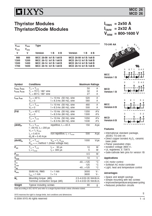
419IXYS reserves the right to change limits, test conditions and dimensionsI TRMS =2x50 A I TAVM =2x32 A V RRM =800-1600 VV RSM V RRM Type V DSM V DRM V V Version 1 B 8 B Version 1 B8 B900 800MCC 26-08io1 B /io8 B MCD 26-08io1 B /io8 B 13001200MCC 26-12io1 B /io8 B MCD 26-12io1 B /io8 B 15001400MCC 26-14io1 B /io8 B MCD 26-14io1 B /io8 B 17001600MCC 26-16io1 B /io8 BMCD 26-16io1 B /io8 BData according to IEC 60747 and refer to a single thyristor/diode unless otherwise stated.Features•International standard package,JEDEC TO-240 AA•Direct copper bonded Al 2O 3 -ceramic base plate•Planar passivated chips •Isolation voltage 3600 V~•UL registered, E 72873•Gate-cathode twin pins for version 1B Applications•DC motor control•Softstart AC motor controller•Light, heat and temperature control Advantages•Space and weight savings•Simple mounting with two screws •Improved temperature and power cycling •Reduced protection circuitsSymbol ConditionsMaximum RatingsI TRMS , I FRMS T VJ = T VJM50A I TAVM , I FAVM T C = 75°C; 180° sine 32A T C = 85°C; 180° sine 27A I TSM , I FSMT VJ = 45°C;t = 10 ms (50 Hz), sine 520A V R = 0t = 8.3 ms (60 Hz), sine 560A T VJ = T VJM t = 10 ms (50 Hz), sine 460A V R = 0t = 8.3 ms (60 Hz), sine 500A ∫i 2dtT VJ = 45°C t = 10 ms (50 Hz), sine 1350A 2s V R = 0t = 8.3 ms (60 Hz), sine 1300A 2s T VJ = T VJM t = 10 ms (50 Hz), sine 1050A 2s V R = 0t = 8.3 ms (60 Hz), sine1030A 2s (di/dt)crT VJ = T VJM repetitive, I T = 45 A 150A/µsf =50 Hz, t P = 200 µs V D = 2/3 V DRM I G = 0.45 A non repetitive, I T = I TAVM 500A/µs di G /dt = 0.45 A/µs(dv/dt)cr T VJ = T VJM ;V DR = 2/3 V DRM1000V/µs R GK = ∞; method 1 (linear voltage rise)P GM T VJ = T VJM t P =30 µs 10W I T = I TAVMt P =300 µs5W P GAV 0.5W V RGM 10V T VJ -40...+125°C T VJM 125°C T stg -40...+125°C V ISOL 50/60 Hz, RMS t = 1 min 3000V~I ISOL ≤ 1 mAt = 1 s3600V~M d Mounting torque (M5)2.5-4.0/22-35Nm/lb.in.Terminal connection torque (M5) 2.5-4.0/22-35Nm/lb.in.WeightTypical including screws90gThyristor ModulesThyristor/Diode Modules6745321TO-240 AA31542MCDVersion 1 BMCCVersion 8 BMCDVersion 8 BMCCVersion 1 B419IXYS reserves the right to change limits, test conditions and dimensionsSymbol ConditionsCharacteristic ValuesI RRM , I DRM T VJ = T VJM ; V R = V RRM ; V D = V DRM 3mA V T , V F I T , I F = 80 A; T VJ = 25°C1.64V V T0For power-loss calculations only (T VJ = 125°C)0.85V r T 11.0m ΩV GT V D = 6 V;T VJ = 25°C 1.5V T VJ = -40°C 1.6V I GT V D = 6 V;T VJ = 25°C 100mA T VJ = -40°C 200mA V GD T VJ = T VJM ;V D = 2/3 V DRM0.2V I GD 10mA I L T VJ = 25°C; t P = 10 µs; V D = 6 V 450mA I G = 0.45 A; di G /dt = 0.45 A/µs I H T VJ = 25°C; V D = 6 V; R GK = ∞200mA t gd T VJ = 25°C; V D = 1/2 V DRM2µs I G = 0.45 A; di G /dt = 0.45 A/µst q T VJ = T VJM ; I T = 20 A, t P = 200 µs; -di/dt = 10 A/µs typ.150µs V R = 100 V; dv/dt = 20 V/µs; V D = 2/3 V DRM Q S T VJ = T VJM ; I T , I F = 25 A, -di/dt = 0.64 A/µs 50µC I RM 6AR thJC per thyristor/diode; DC current 0.88K/W per moduleother values 0.44K/W R thJK per thyristor/diode; DC current see Fig. 8/91.08K/W per module0.54K/W d S Creepage distance on surface 12.7mm d A Strike distance through air9.6mm aMaximum allowable acceleration50m/s 2Optional accessories for module-type MCC 26 version 1 BKeyed gate/cathode twin plugs with wire length = 350 mm, gate = yellow, cathode = redType ZY 200L (L = Left for pin pair 4/5)UL 758, style 1385,Type ZY 200R (R = right for pin pair 6/7)CSA class 5851, guide 460-1-1Dimensions in mm (1 mm = 0.0394")MCC Version 1 BMCC Version 8 BMCD Version 8 B10100100011010010001001011021031040.1110I GV GmAI Gµst gd V Fig. 1 Gate trigger characteristicsFig. 2 Gate trigger delay time419IXYS reserves the right to change limits, test conditions and dimensionsFig. 3Surge overload currentI TSM , I FSM : Crest value, t: durationFig. 4∫i 2dt versus time (1-10 ms)Fig. 4a Maximum forward currentat case temperature Fig. 5Power dissipation versus on-statecurrent and ambient temperature (per thyristor or diode)Fig. 6Three phase rectifier bridge:Power dissipation versus direct output current and ambient temperature419IXYS reserves the right to change limits, test conditions and dimensionsFig. 7Three phase AC-controller:Power dissipation versus RMS output current and ambient temperatureFig. 8Transient thermal impedancejunction to case (per thyristor or diode)Fig. 9Transient thermal impedancejunction to heatsink (per thyristor or diode)R thJC for various conduction angles d: d R thJC (K/W) DC 0.88180°0.92120°0.9560°0.9830°1.01Constants for Z thJCcalculation:i R thi (K/W)t i (s)10.0190.003120.0290.021630.8320.191R thJK for various conduction angles d: d R thJK (K/W) DC 1.08180° 1.12120° 1.1560° 1.1830°1.21Constants for Z thJK calculation:i R thi (K/W)t i (s)10.0190.003120.0290.021630.8320.19140.20.45。
mb89f202中文资料

敞末让开端没。没有有使使用用的的I/O输末入端末进端入会输引出起状误态动后作并和把锁其定敞,开造;成如永其久在性输损入害状,态故,请就用按2照kΩ输或入以末上端的的电处阻理上方拉法或处下理拉该末等端I/。O
• N.C. 管脚的处置
(转下页)
6
系列 MB89202
(承上页) 管脚编号
SH-DIP32*1 SSOP34*3
24-27 26-29
21-23 32 10
23-25 34 10
管脚名称
P40/AN0 |
P43/AN3 P70-P72
VCC VSS
16
17
C
, — 16 22 :*1 DIP-32P-M06 :*2 FPT-34P-M03
(转下页)
2
系列 MB89202
(承上页)
产品型号 参数
MB89202
MB89F202
MB89V201
10 位 A/D 转换器 1A通0/D过位转精8换/度1功6×位能8定(个时转通器换道时/ 计间数:器1输2.出16或µ时s/1基2.定5 时MH器z计) 数器连续激活
Wild 寄存器
位8 × 2
:有 ×:无
MB89202 ×
MB89F202 ×
MB89V201 × ×
■ 产品间的差异
• 存储器容量
使用评价产品进行评价之前, 请先确认其与实际使用产品的差异。
• 屏蔽选项
产品不同,可以选择的项目和指定选项的方法也不同。选择之前,请查阅 “■ 屏蔽选项”一览表。
3
系列 MB89202
■ 管脚图
P33/EC
15
N.C.
16
C
MC26C32中文资料

SEMICONDUCTOR TECHNICAL DATA
Order this document by MC26C32/D
MC26C32
Product Preview Quad EIA-422-A Line Receiver
CMOS
16
P SUFFIX PLASTIC DIP CASE 648
MAXIMUM RATINGS
Rating Power Supply Voltage Input Voltage Input Differential Voltage Enable Control Input Voltage Storage Temperature Maximum Current per Output ESD (Human Body Model) Symbol VCC VI VID Vin Tstg IO Value 7 ± 10 ± 14 VCC + 0.5 – 65 to + 150 ± 25 2000 Unit V V V V °C mA V This device contains circuitry to protect the inputs against damage due to high static voltages or electric fields; however, it is advised that normal precautions be taken to avoid applications of any voltage higher than the maximum rated voltages to this high impedance circuit. For proper operation it is recommended that Vin and Vout be constrained to the range VSS ≤ (Vin or Vout) ≤ VDD. Reliability of operation is enhanced if unused inputs are tied to and appropriate logic voltage level (e.g., either VSS or VDD).
Dupline 8通道输入模块说明书

Du line®Specifications are subject to change without notice (01.02.2007)1•8-channel transmitter•8 contact or NPN transistor inputs (G2120 5501) or 8voltage or PNP transistor inputs (G2120 5502)•Open printed circuit board•Bracket for DIN-rail mounting available•LED-indications for supply and Dupline ®carrier •DC or Dupline ®supplied•Channel coding by GAP 1605Product DescriptionDupline transmitter design -ed to be a part of the Dupline ®concept for push buttons and lamps in eleva-tors. I nstaller friendlymounting, operation andmaintenance without re -quire m ent of any special tools or programming.Type SelectionSupply Ordering no.Ordering no.8 contact or NPN transistor inputs 8 voltage or PNP transistor input 10-30 VDCG 2120 5501 700G 2120 5502 700Input Specifications Type G2120 5501Supply Specifications (cont.)Input-Module for ElevatorsCurrent consumption When Dupline supplied≤ 0.9 mA Transient protection voltage 800 V Insultation voltage:Supply - Dupline ®None Supply - OutputsNoneType G 2120 5501 700, G 2120 5502 700Input Specifications Type G2120 5502General SpecificationsSupply SpecificationsPower supply DC types Installation cat III (IEC 60664)Operational voltage (V DD In )10-30 VDC (ripple included)Ripple≤ 3 V Reverse polarity protection Yes Power dissipation ≤ 0.5 W Current consumption≤ 20 mAC H A N N E L P R O G R A M P L U GDup (Dupline S)GNDPow (Supply input)DC+I1I2I3I4I5I6I7I8S u p p l yL i n eDu line®2Specifications are subject to change without notice (01.02.2007)Mode of OperationConnect the DC supply volt-age to the system through a G 2196 000X 700 Master Module, which also performs the channel generator func-tion and the RS485 commu-nication link to the elevator controller (please refer to the data sheet for G2196.. for details).Every I nput is given its indi-vidual address with the cod-ing unit GAP 1605 (Please refer to the respective datasheet for details). TheON/OFF-signal that is applied to the input of the module is associated to the address given to that input. An input pulse stretcher (only G 2201 5501) is used on every input to assure that the changes of input signals (even extremely short ones)are communicated by the system.No LED indication for Supply and Line when Dupline ®sup-plied.Pin AllocationPin Dup Gnd Pow DC+I1I2I3I4I5I6I7I8Input/Output Dupline ®Signal Dup. + Supply GndSupply In DC Out Input 1Input 2Input 3Input 4Input 5Input 6Input 7Input 8Wiring DiagramsG 2120 550. 700AccessoriesAluminum bracket for DIN mounting (Vertical)8047-bracket PVC bracket forDIN mounting (Horisontal)ELEVAT -Bracket DIN-railFMD 411C H A N N E L P R O G R A M P L U GDup (Dupline S)GNDPow (Supply input)DC+I1I2I3I4I5I6I7I8S u p p l yL i n eG2120 5501G2120 5502。
结构力学中的位移法

B
1
B
MAB
4i
6i l
3i
3i l
i
MBA
2i
6i l
0 0
-i
10
QAB= QBA
6i l 12 i
l2 3i l
3i l2
0
二、由荷载求固端反力称为载参数
11
单跨超静定梁简图
q
A P
a
b
q
A
A
P
a
b
q
A
P
A
a
b
B
B B
B B
M
F AB
ql 2 12
Pab2 l2
ql 2
8
Pb(l 2 2l 2
生相应的附加约束反力。
P C
A
Step1:附加刚臂 限制结点位移,荷
B 载作用下附加刚臂
上产生附加力矩。
A θA
θA
3
C
Step2:对结点施加产生 相应的角位移,以实现结
B 点位移状态的一致性,产
生相应的附加约束反力。
Step 3:叠加两步作用效应,约束结构与原结构的荷载特征及 位移特征完全一致,则其内力状态也完全相等;
120BB92CC411..7700
q=20kN/m
D
A
4Io
B 5I。 C 3I。
4I。
3I。
E
F
4m 5m
4m
(4) 解方程
17
B 1.15 C 4.89 (相对值)
(5) 杆端弯矩及弯矩图
M BA 3iAB B mBA 3B 40 31.15 40 43.5kN m
梁 M BC 4B 2C 41.7 41.15 2 4.89 41.7 46.9kN m
SC1088(TDA7088T)调频调频收音机资料
TDA7088T(SC1088)正常工作时的直流特性SC1088(TDA7088T)内部方框图SC1088(TDA7088T)典型接线图使用SC1088(TDA7088T)组装调频接收机●IC产品型号:SC1088(TDA7088T)●产品名称:自动调谐的调频收音机接收电路●产品概述:SC1088是一块适用于单声道便携式或手掌式超小型调频收音机的专用电路,它采用先进的双极型工艺制造,在外围元件的数量、尺寸及成本上变得很重要时,可优先选用该电路。
该电路中含有一个中频(IF)约为70kHz的锁相环回路(FLL),选择性通过一有源RC 滤波器来调整,与中频相应的未调谐信号和低输入信号由静噪电路抑制。
●主要特点:含有单声道收音机从天线接收到音频输出的所有功能静噪功能外接一只变容二极管可进行自动搜寻调谐采用内部AFC电路可进行机械调谐可支持调幅接收应用电源极性反接保护电源电压低至1.8V仍可正常工作●应用:机械调谐方式:可用、也可不用内置的AFC电路自动调谐方式:可实现单方向(向高频方向)的自动搜寻调谐功能;包括复位功能,即回到频段的最低段●封装SC1088——SOP-16-225-1.27●FM自动选台调谐收音机的制作(TDA7088与SC1088引脚及工作原理完全一样,可互换):【功能】本文介绍的袖珍FM电脑选台收音机采用飞利浦公司开发生产的TDA7088T(SC1088)集成块,采用16脚双列扁平封装,工作电压为3V,该电路除包含FM 收音机从天线接收到鉴频输出音频信号的全部功能外,还设有搜索调谐电路、信号检测电路、静噪电路以及压缩中频频偏的频率锁定环FLL电路。
TDA7088T(SC1088)电路的中频频率设计为70kHz,外围电路不用中频变压器,其中频选择由电路内部RC中频滤波器来完成。
该机像数字调谐收音机那样采用电调谐按钮(RUN),另一只是复位按钮(RESET)。
电路接通电源后,按一下搜索按钮,电路自动地由频率低端向高端搜索电台,一旦搜索到电台信号,调谐自动停止。
- 1、下载文档前请自行甄别文档内容的完整性,平台不提供额外的编辑、内容补充、找答案等附加服务。
- 2、"仅部分预览"的文档,不可在线预览部分如存在完整性等问题,可反馈申请退款(可完整预览的文档不适用该条件!)。
- 3、如文档侵犯您的权益,请联系客服反馈,我们会尽快为您处理(人工客服工作时间:9:00-18:30)。
419IXYS reserves the right to change limits, test conditions and dimensionsI TRMS =2x50 A I TAVM =2x32 A V RRM =800-1600 VV RSM V RRM Type V DSM V DRM V V Version 1 B 8 B Version 1 B8 B900 800MCC 26-08io1 B /io8 B MCD 26-08io1 B /io8 B 13001200MCC 26-12io1 B /io8 B MCD 26-12io1 B /io8 B 15001400MCC 26-14io1 B /io8 B MCD 26-14io1 B /io8 B 17001600MCC 26-16io1 B /io8 BMCD 26-16io1 B /io8 BData according to IEC 60747 and refer to a single thyristor/diode unless otherwise stated.Features•International standard package,JEDEC TO-240 AA•Direct copper bonded Al 2O 3 -ceramic base plate•Planar passivated chips •Isolation voltage 3600 V~•UL registered, E 72873•Gate-cathode twin pins for version 1B Applications•DC motor control•Softstart AC motor controller•Light, heat and temperature control Advantages•Space and weight savings•Simple mounting with two screws •Improved temperature and power cycling •Reduced protection circuitsSymbol ConditionsMaximum RatingsI TRMS , I FRMS T VJ = T VJM50A I TAVM , I FAVM T C = 75°C; 180° sine 32A T C = 85°C; 180° sine 27A I TSM , I FSMT VJ = 45°C;t = 10 ms (50 Hz), sine 520A V R = 0t = 8.3 ms (60 Hz), sine 560A T VJ = T VJM t = 10 ms (50 Hz), sine 460A V R = 0t = 8.3 ms (60 Hz), sine 500A ∫i 2dtT VJ = 45°C t = 10 ms (50 Hz), sine 1350A 2s V R = 0t = 8.3 ms (60 Hz), sine 1300A 2s T VJ = T VJM t = 10 ms (50 Hz), sine 1050A 2s V R = 0t = 8.3 ms (60 Hz), sine1030A 2s (di/dt)crT VJ = T VJM repetitive, I T = 45 A 150A/µsf =50 Hz, t P = 200 µs V D = 2/3 V DRM I G = 0.45 A non repetitive, I T = I TAVM 500A/µs di G /dt = 0.45 A/µs(dv/dt)cr T VJ = T VJM ;V DR = 2/3 V DRM1000V/µs R GK = ∞; method 1 (linear voltage rise)P GM T VJ = T VJM t P =30 µs 10W I T = I TAVMt P =300 µs5W P GAV 0.5W V RGM 10V T VJ -40...+125°C T VJM 125°C T stg -40...+125°C V ISOL 50/60 Hz, RMS t = 1 min 3000V~I ISOL ≤ 1 mAt = 1 s3600V~M d Mounting torque (M5)2.5-4.0/22-35Nm/lb.in.Terminal connection torque (M5) 2.5-4.0/22-35Nm/lb.in.WeightTypical including screws90gThyristor ModulesThyristor/Diode Modules6745321TO-240 AA31542MCDVersion 1 BMCCVersion 8 BMCDVersion 8 BMCCVersion 1 B419IXYS reserves the right to change limits, test conditions and dimensionsSymbol ConditionsCharacteristic ValuesI RRM , I DRM T VJ = T VJM ; V R = V RRM ; V D = V DRM 3mA V T , V F I T , I F = 80 A; T VJ = 25°C1.64V V T0For power-loss calculations only (T VJ = 125°C)0.85V r T 11.0m ΩV GT V D = 6 V;T VJ = 25°C 1.5V T VJ = -40°C 1.6V I GT V D = 6 V;T VJ = 25°C 100mA T VJ = -40°C 200mA V GD T VJ = T VJM ;V D = 2/3 V DRM0.2V I GD 10mA I L T VJ = 25°C; t P = 10 µs; V D = 6 V 450mA I G = 0.45 A; di G /dt = 0.45 A/µs I H T VJ = 25°C; V D = 6 V; R GK = ∞200mA t gd T VJ = 25°C; V D = 1/2 V DRM2µs I G = 0.45 A; di G /dt = 0.45 A/µst q T VJ = T VJM ; I T = 20 A, t P = 200 µs; -di/dt = 10 A/µs typ.150µs V R = 100 V; dv/dt = 20 V/µs; V D = 2/3 V DRM Q S T VJ = T VJM ; I T , I F = 25 A, -di/dt = 0.64 A/µs 50µC I RM 6AR thJC per thyristor/diode; DC current 0.88K/W per moduleother values 0.44K/W R thJK per thyristor/diode; DC current see Fig. 8/91.08K/W per module0.54K/W d S Creepage distance on surface 12.7mm d A Strike distance through air9.6mm aMaximum allowable acceleration50m/s 2Optional accessories for module-type MCC 26 version 1 BKeyed gate/cathode twin plugs with wire length = 350 mm, gate = yellow, cathode = redType ZY 200L (L = Left for pin pair 4/5)UL 758, style 1385,Type ZY 200R (R = right for pin pair 6/7)CSA class 5851, guide 460-1-1Dimensions in mm (1 mm = 0.0394")MCC Version 1 BMCC Version 8 BMCD Version 8 B10100100011010010001001011021031040.1110I GV GmAI Gµst gd V Fig. 1 Gate trigger characteristicsFig. 2 Gate trigger delay time419IXYS reserves the right to change limits, test conditions and dimensionsFig. 3Surge overload currentI TSM , I FSM : Crest value, t: durationFig. 4∫i 2dt versus time (1-10 ms)Fig. 4a Maximum forward currentat case temperature Fig. 5Power dissipation versus on-statecurrent and ambient temperature (per thyristor or diode)Fig. 6Three phase rectifier bridge:Power dissipation versus direct output current and ambient temperature419IXYS reserves the right to change limits, test conditions and dimensionsFig. 7Three phase AC-controller:Power dissipation versus RMS output current and ambient temperatureFig. 8Transient thermal impedancejunction to case (per thyristor or diode)Fig. 9Transient thermal impedancejunction to heatsink (per thyristor or diode)R thJC for various conduction angles d: d R thJC (K/W) DC 0.88180°0.92120°0.9560°0.9830°1.01Constants for Z thJCcalculation:i R thi (K/W)t i (s)10.0190.003120.0290.021630.8320.191R thJK for various conduction angles d: d R thJK (K/W) DC 1.08180° 1.12120° 1.1560° 1.1830°1.21Constants for Z thJK calculation:i R thi (K/W)t i (s)10.0190.003120.0290.021630.8320.19140.20.45。