RTL8306E-8306M-8304E开发包
各主板型号里的字母

各主板型号里的字母代表啥意思。
先从一线大品牌说起吧:华硕(ASUS)枝嘉(GIGABYTE)微星(MSI)华硕与枝嘉和微星主板命名方式比确实复杂一些,华硕主板型号主要分为:ABCD-EF六个区域。
如主板M4A88TD-M,其中A区域代表CPU的插座种类,目前还能大量见到的M2(AMD,AM2)M3(AMD,am2+/am2)M4(AMD,am3)P5(Intel,LGA775) P6(Intel , LGA1366) P7(Intel ,LGA1156)支持最新的Intel LGA1155 Sandy Bridge处理器的6系列主板则被命名为P8。
可以发现,该区域数字的递增(2-4,5-8)分别与两家厂商CPU插座更迭的时间顺序一致。
故上主板M4代表支持aM3 插槽的CPU。
B区表示主板芯片组如:I平台P55代表主板用了Intel P55的芯片组A平台A78 是用了AMD 780G芯片组 A88就是采用的AMD 880G 芯片组C区表示主板支持的内存规格。
字母为C 表示支持DDR2和DDR3两种内存字母为T 表示只支持DDR3内存这为用户辨别规格提供方便,但懂次代表字母意义的并不多。
D区代表是否拥有华硕巅峰设计(stock cook3)有则有字母D,没有则空。
E区表示主板的版型通常说的大阪小板。
(M等于Micro atx小板,atx 大板)V表示具有显示输出功能的ATX。
(普通板ATX版型此处为空)M4A88TD-M 说明是小板。
F区代表产品的系列,除了大家耳熟能详的PRO(Professional),EVO(Evolution),Deluxe,Premium四个中高端系列(定位高于标准版,由低到高)以外,拥有LE,LE2,LX后缀的华硕主板分别为超值版,超值版2和入门超值版(定位低于标准版,由高到低),没有此项后缀的产品自然就是标准版啦。
M4A78LT-MLE 后缀LE表示定位比标准版稍低一些。
中兴交换机配置

一、系统的启动过程如下。
1、上电后,首先进行硬件启动,当硬件检测无误后,管理终端上出现下列信息:Welcome to use ZTE eCarrier!!Copyright(c) 2004-2006, ZTE Co。
, Ltd.System Booting..。
.。
CPU: S3C45010 ARM7TDMIBSP version: 1.2/0Creation date: Feb 11 2004, 09:37:01Press any key to stop auto-boot。
..72、出现上述信息后,等待大约7 秒,用户可以在这段时间内按任意键进入boot 状态,修改启动参数.当系统在规定时间未检测到用户输入时,系统便开始自动加载版本,并提示下列信息:auto—booting。
..boot device : secEndunit number : 0processor number : 0host name : tigerfile name : vxWorksinet on ethernet (e) : 10.40.92。
106host inet (h) : 10。
40.92.105flags (f) : 0x80Attaching to TFFS.。
done。
Loading version:/kernel.。
.1459932 + 75292 + 6358852Starting at 0x1656e0...Attaching interface lo0。
.。
done(省略)Welcome !ZTE Corporation。
All rights reserved.login:adminpassword:*********3、系统启动成功后,出现提示符login:,要求输入登录用户名和密码,缺省用户名是admin,密码是zhongxing。
二、配置开始工作1.打开超级终端,输入连接的名称,如ZXR10,并选择一个图标。
开关电源常用芯片

FSGM0765RWDTUFSL106HR 、FSL106MR 、FSL116LR 、开关电源常用芯片FSCQ1265RTYDTU 、 FSCQ1565RTYDTUFSDL321FSDH321 、FSDL0165RN 、FSDM0265RNB 、FSDH0265RN 、 FSDM0365RNB 、 FSDL0365RN 、 FSDM0465REWDTUFSDM0565REWDTU 、FSDM07652REWDTU FSDM311A 、FSEZ1016AMY 、 FSEZ1317NY 、Fairchild 仙童(飞兆)系列开关电源驱动芯片FAN100MY 、 FAN102MY 、FAN103MY 、 FAN6208 、 FAN6300AMY 、 FAN6754AMRMY 、FAN6862TY 、FAN6921MRMY 、FAN6961SZ 、FAN7346MX 、FAN7384MX 、 FAN7319MX 、FAN7527BMX 、FAN7527BN 、FAN7554N 、 FAN7554DFAN7621 、FAN7621SSJ 、FAN7621B 、FAN7631 、 FAN7930CMX ;FAN6204MYFL103 、FL6300A 即 FAN6300 、 FL6961 、FL7701 、FL7730 、FL7732 、FL7930B 、FLS0116 、FLS3217 、FLS3247 、FLS1600XS 、FLS1800XS 、 FLS2100XSFSFR1600 、 FSFR1600XSL 、 FSFR1700 、FSFR1700XS 、FSFR1700XSL 、FSFR1800 、 FSFR1800XS 、 FSFR1800XSL 、FSFR2100XSL 、FSFR2100FSCQ0565RTYDTU 、FSCQ0765RTYDTU、FSDM311 、FSEZ1317MYFSGM0465RWDTU 、FSGM0565RWDTUSD4569 )、ME8204 (兼容 SG6848 、OB2263 、OB2273 、 FSQ0565RSWDTUSG6105ADZ 、 SG6859ATZ 、SG5842KA5L0380RYDTU 、 KA5M0365RYDTUKA5M0365RTU 、KA5M0380RYDTU 、 KA3525A 、KA3842AC 、KA3842AE 、KA3842B 、KA3843B 、KA3844B 、 KA7500Con-bright 昂宝系列电源驱动芯片超低待机功耗产 品系列:OB5269、OB5269B 、OB2273、OB2273A 、OB2273B 、 OB2273F 、OB2273N 、OB2276 、OB2276A 原边控制系列产品: OB2520 、OB2520D 、OB2520M 、OB2532 、OB2531 ; OB2535/OB2535E 、OB2536/OB2536E 、OB2538/OB2538E OB2539 、OB2211 、OB2211H 、OB2212 、OB2216 准谐振 模式控制芯片系列: OB2201/T 、 OB2202 、 OB2203PWM 控制芯片系列产品: OB5269 、 OB5269B 、OB2273 、 OB2273A 、OB2273B 、OB2273F 、 OB2273N 、OB2361 、 OB2361P 、OB2262 、OB2263 、OB2268 、OB2269 、OB2279 、OB2287 、OB2288 、OB2298 、OB5222 、OB5225 、 OB2353/L 、OB2354/L 、OB2356/L 、OB2357/L 、OB2358/L 功率因子校正控制芯片: OB6573 、OB6572 、 OB6561P 、 OB6563 、OB6663LED 照明驱动系列: OB3330 、OB3340 、 OB3390/T 、 OB3391 、 OB3394 、OB3396 、OB3380 、 FSL206MRN 、FSL126MR 、FSL136MR 、FSQ100 、FSQ110 、 FSQ321 、FSQ510 、 FSQ0165RN 、 FSQ0170RNA 、 FSQ0265RN 、FSQ0270RNA 、FSQ0365RN 、FSQ0370RNA 、SN03ABCD 系列电源驱动芯片 PSR Controller :AP3703 、 AP3706 、AP3708N 、AP3760 、AP3765 、AP3766 、AP3768 、AP3769S 、AP3770 、AP3771 、AP3772Voltage Mode PWM Controller : AZ494A 、 AZ494C 、 AZ7500B 、 AZ7500C 、AZ7500E 、AZ7500FGreen Mode PWM Controller :AP3101 、AP3105/AP3105V/AP3105L/AP3105R AP3105/AP3105H ; AP3700 、 AP3700A 、AP3700E 、 AP3710Secondary Side Controller : AP4305 、 AP4306A 、AP4306B 、AP4313 、AP4310A 、 AP4340LED 照明 PFCME8101 (内置 13003 兼容THX203/RM6203/GW6203/CR6203 )、ME8105 (内置13003 兼容 THX203/RM6203/GW6203/CR6203机功能)、 ME8109A (内置 2N65 兼容 OB2358/AP8022 )、 ME8109B (内置 2N60 兼容 OB2358/AP8022 )、 ME8119 AP3102/AP3102V/AP3102L 、 AP3103 、、 AP3106 、 controller : AP1661/AP1661E AP1661A 、 AP1662 ; PSRcontroller : AP1681 (可调光)、 AP1682 、 AP1686microne 南京微盟系列开关电源驱动芯片 ME8100( 兼容 ATC30B ) 、,具有防炸(内置4N60 )、ME8110 (内置2N65 兼容OB2358 )、ME8200兼容SG6848 、OB2263 、LD7535 、GR8835 、SD456 )、ME8202 (兼容SG5841 、OB2269 、LD7552 、GR8841 、SD4569 )、ME8204 (兼容SG6848 、OB2263 、OB2273 、RM3261S 、 RM3261D 、RM3262D ; PFM 控制芯片系列: RM3252T 、 RM3260T 、RM3260DQR 控制芯片系列: RM6401S 、 RM6401D ;PFC+QR+PWM 控制芯片系列: RM6901S 、 RM6901Dchiplink-semi 南京芯联系列开关电源 驱动芯片 AC/DC PSR : CL1132 、CL1128 、 CL1101 、 LD7535 、 GR8835 、SD456 )、ME8300 (兼容 AP3708 )、 ME8302 (兼容 AP3768 )、ME8304 (兼容 AP3765 , AP3706 SOP8) )、ME8305 (内置 13003 兼容 AP3765 ,AP3706 SOP8) )、ME8315chiprail 成都启达系列开关电源驱动芯 片绿色节能 PWM/PFC 控制器: CR6848 、CR6850D 、 CR6853 、CR6842 、CR6845 、CR6855 、CR6232C 、CR6233 、CR5201 、CR6562 绿色节能 PWM 功率开关: CR5336 、CR5337 、CR5202 、CR5223 、CR5224 、CR5228 、 CR5229reactor-micro 陕西亚成微系列开关电源驱动芯片 RM3253S 、RM3253D 、RM3263S 、 RM3263D 、RM3261S 、RM3261D 、RM3262D 、RM3260T 、 RM3260D 、RM6203 、RM6204 、RM6221S 、 RM6221D 、 RM6222D 、RM6220T 、RM6401S 、RM6401S 、RM337X (1/2/3) 、RM3370T 、RM6901SPWM 功率开关芯片 RM6203D 、RM6204D 、RM6221S 、RM6221D 、 RM6222D ;PWM 控制芯片系列: RM6220TPFM 功率开关 RM3253S 、RM3253D 、RM3263S 、RM3263D 、 CR5335、 LED 照明驱动系列: 系列: 芯片系列:CL1100 ;PSR+MOS:CL1129 、CL1112 、CL1107 、CL1103PFC :CL6562 ;Flyback with MOSFET :CL1152 ;Flyback :CL1156 、CL1160 、CL1158Lighting LED Driver :CL0122 、CL0119A 、CL0118 、CL0116A 、CL0117 、CL6563A 、CL1158 、CL1112 、CL1129 、CL1128 、CL1101 、CL1100 、CL6809 、CL6808 、CL6807 、CL6804 ;Back Light Driver :CL6201sifirsttech 南海赛威系列开关电源驱动芯片AC/DC PWM Controller :SF1530 、SF1530U 、SF1531 、SF1531S 、SF1560 、SF1563 、SF1565 、SF1580 、SF1585 、SF1590 、SF1595 、SF5580 ;超低待机功耗AC/DC PWM 控制器IC :SF5533 、SF5534 、SF5545B 、SF5545 、SF5547AC/DC PWM Power Switch :SF1532 、SF1533 、SF1536 、SF1537 、SF1538 、SF1539 、SF1539HT 、SF1548 、SF1549 、SF5582H 、SF5582 、SF5590 ;原边反馈控制器/功率开关IC :SFL628 、SFL629 、SFL900 、SF5920S 、SF5920 、SF5922 、SF5922T 、西安民展微系列开关电源驱动芯片绿色节能PWM 功率转化、SF5922SV 、SF5926SV 、SF5926 、SF5928SV 、SF5922SSF5928S 、SF5928 、SF6010L 、SF6010F 、SF6018、SF6040 、SF6070 、SF6072 、SF6771 、SF6772 、SF6778 、SF6781 、SF6782 、SF6788 功率因子校正器IC :SFL320 、SF6562 、SFL500 、SF6563 、SF6566 ;LED 照明驱动IC :SFL330 、SFL520 、S FL668 、SFL669 、SFL678 、SF6010power-railSDC4569si-power 无锡硅动力系列开关电源驱动芯片SDC4569si-power 无锡硅动力系列开关电源驱动芯片PR6239 、CR6235S 、CR6236T 、 CR6238T 绿色节能 PWM 功率转化器系列 (PWM 控制芯片 + 600V MOSFET) 反激式 PR8224 、 PR8224H 、 CR6221T 、 CR6224S 、CR6224T 、CR6228T 、CR6229T 、 PR8612 绿 色节能 PWM 控制器系列 Primary Side Regulation 初级端 调节 PR6234 、CR6232PR6863 、PR9853 、 CR6850C 、 PR8278 、PR8278B 、PR8275 、PR6599 、PR6562 、CR6561 、CR6563 、PR8910 、PR3845Bbpsemi 上海晶丰明源系列开 关电源驱动芯片高功率因数高效率隔离恒流驱动芯片:BP2802 、 BP2808B 、BP2818 、 BP2812 、BP2822 高精度 BP3105 、BP3102 、 BP3122 、 BP3123 、BP3115 、BP3125 、 BP3108BP2309 、BP5118 、 BP1360 、BP1361 、BP1601maxictech 驱动芯片 MT7933 、MT7930 、MT7952 、MT7953 、MT7955 、 MT7950 、MT7801 、MT7838 、MT7200 、MT7201 、MT7261 、 MT7281 、MT7004Bsdc-semi 绍兴光大系列开关电源驱动芯 片 SDC602 、 SDC603 、SDC606 、SDC608 、SDC3842 、 SDC3843 、SDC3844 、SDC3845 、SDC4108 、SDC4108L 、 SDC4109 、 SDC4109L 、 SDC4563 、 SDC4565 、器系列 (PWM 控制芯片 + 600V MOSFET) 初级端调 节 :PR6237 、BP3309 、B P3308 高效率非隔离恒流驱动芯片: BP2808 、 高效率隔离恒流驱动芯片: 美芯晟系列开关电源SP5629P 、SP5619P 、SP5876P 、SP5876F 、SP5875P 、SP5875F 、SP5518F 、SP5808F 、5508F 、SP5506 、SP5505SP5615/6/8 可以代替OB2535/6/8 用于低功耗AC/DC 适配器的详细描述:SP5615 是一颗高精度离线式开关电源电路,应用于低功耗AC/DC 充电器与适配器。
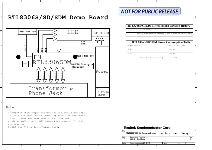
RTL8306SD(M)_DEMO-SCH128P
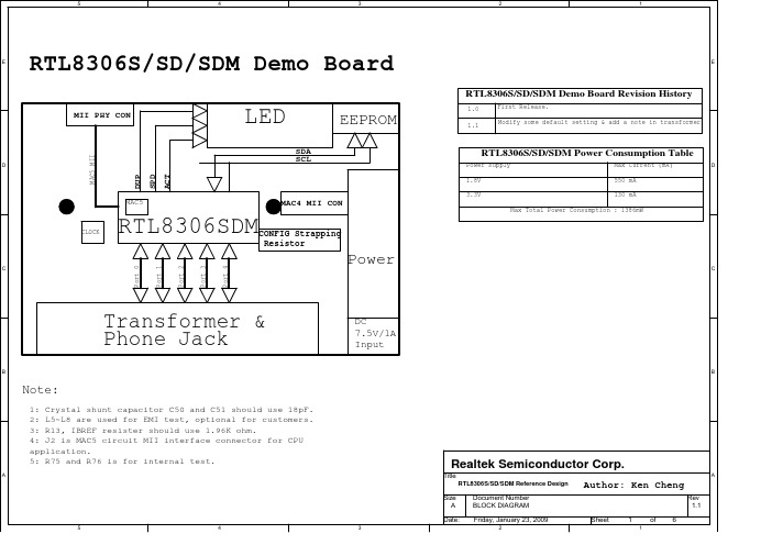
EEPROM1.1DMAC5 MII
RTL8306S/SD/SDM Power Consumption Table
Power supply 1.8V 3.3V Max Current (mA) 550 mA 130 mA Max Total Power Consumption : 1386mW
D
MAC5
5
4
3
2
1
E
RTL8306S/SD/SDM Demo Board
RTL8306S/SD/SDM Demo Board Revision History
MII PHY CON
E
LED
SDA SCL DUP SPD ACT
1.0
First Release. Modify some default setting & add a note in transformer
PHY2PTXD2 PHY2PTXD1 PHY2PTXD0 PHY2PTXEN PHY2PTXC PHY2PRXC PHY2PRXDV
PHY2PRXD3 PHY2PRXD2 PHY2PRXD1 SDA_MDIO SCL_MDC PHY2PRXD0
MRXD3_PTXD3 MRXD2_PTXD2
ENDEFER PHY2PCOL PHY2PTXD3
P4LNKSTA# (5,6) P4LNKSTA# P4SPDSTA (5,6) P4SPDSTA P4DUPSTA_HMPGCRS (5,6) P4DUPSTA_HMPGCRS P4FLCTRL_CPUINT# (5,6) P4FLCTRL_CPUINT#
MAC4 MII Stapping
C
(5,6) DISDUALMII (5,6) P4MODE1 (5,6) P4MODE0 (5,6) GXMODE (3,5,6) DUP3_GYMODE
RTL8316D_RTL8324D 八口16口交换机网卡数据手册
RTL8316DLAYER 2 16-PORT 10/100M SINGLE CHIPSWITCH CONTROLLERRTL8324DLAYER 2 24-PORT 10/100M SWITCHCONTROLLER WITH ONE RS8MIIDATASHEET(CONFIDENTIAL: Development Partners Only)Rev. 1.016 January 2010Track ID: JATR-2265-11No. 2, Innovation Road II, Hsinchu Science Park, Hsinchu 300, TaiwanTel.: +886-3-578-0211 Fax: +886-3-577-6047Layer 2 16-Port & 24-Port 10/100M Switch Controllers ii Track ID: JATR-2265-11 Rev. 1.0COPYRIGHT©2010 Realtek Semiconductor Corp. All rights reserved. No part of this document may be reproduced, transmitted, transcribed, stored in a retrieval system, or translated into any language in any form or by any means without the written permission of Realtek Semiconductor Corp.DISCLAIMERRealtek provides this document “as is”, without warranty of any kind. Realtek may make improvements and/or changes in this document or in the product described in this document at any time. This document could include technical inaccuracies or typographical errors.TRADEMARKSRealtek is a trademark of Realtek Semiconductor Corporation. Other names mentioned in this document are trademarks/registered trademarks of their respective owners.USING THIS DOCUMENTThis document is intended for the hardware and software engineer’s general information on the Realtek RTL8316D/RTL8324D chips.Though every effort has been made to ensure that this document is current and accurate, more information may have become available subsequent to the production of this guide.REVISION HISTORYRevision Release Date Summary 1.0 2010/01/16 First Release.Table of Contents1.GENERAL DESCRIPTION (1)2.FEATURES (2)3.BLOCK DIAGRAMS (3)3.1.RTL8316D B LOCK D IAGRAM (3)3.2.RTL8324D B LOCK D IAGRAM (4)4.SYSTEM APPLICATIONS (5)4.1.RTL8316D:16*10/100M S WITCH (5)4.2.RTL8324D:24*10/100M S WITCH (6)5.PIN ASSIGNMENTS AND DESCRIPTIONS (RTL8316D) (7)5.1.P IN A SSIGNMENTS F IGURE (RTL8316D) (7)5.2.P ACKAGE I DENTIFICATION (7)5.3.P IN A SSIGNMENTS T ABLE D EFINITIONS (RTL8316D) (8)5.4.P IN A SSIGNMENTS T ABLE (RTL8316D) (8)5.5.P IN D ESCRIPTIONS (RTL8316D) (10)5.5.1.Media Connection Pins (RTL8316D) (10)5.5.2.Serial LED/LED IC Interface Pins (RTL8316D) (11)5.5.3.SCAN LED Interface Pins (RTL8316D) (11)5.5.4.Miscellaneous Interface Pins (RTL8316D) (11)5.5.5.GPIO Interface Pins (RTL8316D) (12)5.5.6.Configuration Strapping Pins (RTL8316D) (12)5.5.7.Power and GND Pins (RTL8316D) (13)6.PIN ASSIGNMENTS AND DESCRIPTIONS (RTL8324D) (14)6.1.P IN A SSIGNMENTS F IGURE (RTL8324D) (14)6.2.P ACKAGE I DENTIFICATION (14)6.3.P IN A SSIGNMENTS T ABLE D EFINITIONS (RTL8324D) (15)6.4.P IN A SSIGNMENTS T ABLE (RTL8324D) (15)6.5.P IN D ESCRIPTIONS (RTL8324D) (17)6.5.1.Media Connection Pins (RTL8324D) (17)6.5.2.Serial LED Interface Pins (RTL8324D) (18)6.5.3.Miscellaneous Interface Pins (RTL8324D) (18)6.5.4.GPIO Interface Pins (RTL8324D) (18)6.5.5.Configuration Strapping Pins (RTL8324D) (19)6.5.6.RS8MII Interface Pins (RTL8324D) (19)6.5.7.Power and GND Pins (RTL8324D) (20)7.PHYSICAL LAYER FUNCTIONAL OVERVIEW (21)7.1.MDI I NTERFACE (21)7.2.100B ASE-TX T RANSMIT F UNCTION (21)7.3.100B ASE-TX R ECEIVE F UNCTION (21)7.4.10B ASE-T T RANSMIT F UNCTION (21)7.5.10B ASE-T R ECEIVE F UNCTION (21)7.6.A UTO-N EGOTIATION FOR UTP (22)7.7.C ROSSOVER D ETECTION AND A UTO C ORRECTION (22)7.8.P OLARITY C ORRECTION (22)8.SWITCH FUNCTION DESCRIPTION (23)8.1.H ARDWARE R ESET AND S OFTWARE R ESET (23)Layer 2 16-Port & 24-Port 10/100M Switch Controllers iii Track ID: JATR-2265-11 Rev. 1.08.1.2.Software Reset (23)8.2.L AYER 2L EARNING AND F ORWARDING (23)8.2.1.Forwarding (23)8.2.2.Learning (24)8.2.3.Address Table Aging (24)8.3.L AYER 2M ULTICAST AND IP M ULTICAST (24)8.4.R ESERVED M ULTICAST A DDRESS H ANDLING (24)8.5.IEEE802.3X F LOW C ONTROL (25)8.6.H ALF D UPLEX B ACKPRESSURE (25)8.6.1.Collision-Based Backpressure (Jam Mode) (25)8.6.2.Carrier-Based Backpressure (Defer Mode) (26)8.7.P RE-IEEE802.3AZ E NERGY E FFICIENT E THERNET (EEE) (26)8.8.G REEN E THERNET (27)8.8.1.Link Down Power Saving (27)8.8.2.Link On Various Cable Length Power Saving (27)8.9.IEEE802.1P AND IEEE802.1Q(VLAN) (27)8.10.L OOP D ETECTION (27)8.11.L AYER 2T RAFFIC S UPPRESSION (S TORM C ONTROL) (27)8.12.IEEE802.3AD L INK A GGREGATION P ROTOCOL (28)8.13.B ANDWIDTH C ONTROL (28)8.13.1.Input Bandwidth Control (28)8.13.2.Output Bandwidth Control (28)8.14.Q UALITY OF S ERVICE (Q O S) (28)8.14.1.Priority Arbitration (28)8.14.2.Port-Based Priority Assignment (28)8.14.3.IEEE 802.1Q-Based Priority Assignment (29)8.14.4.DSCP-Based Priority Assignment (29)8.14.5.Internal Priority to Queue ID Table (29)8.15.P ACKET S CHEDULING (WRR AND WFQ) (29)8.16.E GRESS P ACKET R EMARKING (29)8.17.I NGRESS AND E GRESS P ORT M IRROR (30)8.18.M ANAGEMENT I NFORMATION B ASE (MIB) (30)8.19.R EALTEK C ABLE T ESTER (30)8.20.EEPROM C ONFIGURATION (31)8.21.CPU F UNCTION D ESCRIPTION (31)9.INTERFACE DESCRIPTIONS (32)9.1.RS8MII I NTERCONNECTION (32)9.2.I2C-L IKE LED (32)9.3.S ERIAL LED C ONNECTION (33)9.4.S CAN LED FOR RTL8316D (34)9.5.I2C M ASTER FOR EEPROM (35)9.6.I2C S LAVE FOR E XTERNAL CPU (35)10.ELECTRICAL AC/DC CHARACTERISTICS (36)10.1.A BSOLUTE M AXIMUM R ATINGS (36)10.2.O PERATING R ANGE (36)10.3.DC C HARACTERISTICS (36)10.4.AC C HARACTERISTICS (37)10.4.1.RS8MII Transmitter Signal Electrical Characteristics (37)10.4.2.RS8MII Receiver Signal Electrical Characteristics (37)10.4.3.Serial LED Signal Timing (37)10.4.4.Scan LED Mode Signal Timing (RTL8316D) (38)10.4.5.I2C Master for EEPROM Timing (38)Layer 2 16-Port & 24-Port 10/100M Switch Controllers iv Track ID: JATR-2265-11 Rev. 1.010.4.7.EEPROM Auto-Load Timing (39)10.4.8.I2C Master Mode Timing Characteristics (39)10.4.9.I2C Slave Mode Timing (40)10.4.10.I2C Slave Mode Timing Characteristics (40)11.PACKAGE INFORMATION (41)11.1.LQFP128E-PAD (41)12.ORDERING INFORMATION (42)List of TablesT ABLE 1.P IN A SSIGNMENTS T ABLE (RTL8316D) (8)T ABLE 2.M EDIA C ONNECTION P INS (RTL8316D) (10)T ABLE 3.S ERIAL LED/LED IC I NTERFACE P INS (RTL8316D) (11)T ABLE 4.SCAN LED I NTERFACE P INS (RTL8316D) (11)T ABLE 5.M ISCELLANEOUS I NTERFACE P INS (RTL8316D) (11)T ABLE 6.GPIO I NTERFACE P INS (RTL8316D) (12)T ABLE 7.C ONFIGURATION S TRAPPING P INS (RTL8316D) (12)T ABLE 8.P OWER AND GND P INS (RTL8316D) (13)T ABLE 9.RTL8324D P IN A SSIGNMENTS T ABLE (RTL8324D) (15)T ABLE 10.M EDIA C ONNECTION P INS (RTL8324D) (17)T ABLE 11.LED I NTERFACE P INS (RTL8324D) (18)T ABLE 12.M ISCELLANEOUS I NTERFACE P INS (RTL8324D) (18)T ABLE 13.GPIO I NTERFACE P INS (RTL8324D) (18)T ABLE 14.C ONFIGURATION S TRAPPING P INS (RTL8324D) (19)T ABLE 15.RS8MII I NTERFACE P INS (RTL8324D) (19)T ABLE 16.P OWER AND GND P INS (RTL8324D) (20)T ABLE 17.R ESERVED M ULTICAST A DDRESS D EFAULT A CTIONS (24)T ABLE 18.A BSOLUTE M AXIMUM R ATINGS (36)T ABLE 19.R ECOMMENDED O PERATING R ANGE (36)T ABLE 20.DC C HARACTERISTICS (36)T ABLE 21.RS8MII T RANSMITTER S IGNAL E LECTRICAL C HARACTERISTICS (37)T ABLE 22.RS8MII R ECEIVER S IGNAL E LECTRICAL C HARACTERISTICS (37)T ABLE 23.I2C M ASTER M ODE T IMING C HARACTERISTICS (39)T ABLE 24.I2C S LAVE M ODE T IMING C HARACTERISTICS (40)T ABLE 25.O RDERING I NFORMATION (42)Layer 2 16-Port & 24-Port 10/100M Switch Controllers v Track ID: JATR-2265-11 Rev. 1.0List of FiguresF IGURE 1.RTL8316D B LOCK D IAGRAM (3)F IGURE 2.RTL8324D B LOCK D IAGRAM (4)F IGURE 3.RTL8316D:16*10/100M S WITCH (5)F IGURE 4.RTL8324D:24*10/100M S WITCH (6)F IGURE 5.P IN A SSIGNMENTS (RTL8316D) (7)F IGURE 6.P IN A SSIGNMENTS (RTL8324D) (14)F IGURE 7.C ONCEPTUAL E XAMPLE OF P OLARITY C ORRECTION (22)F IGURE 8.T X P AUSE F RAME F ORMAT (25)F IGURE 9.F LOW C ONTROL S TATE M ACHINE (25)F IGURE 10.C OLLISION-B ASED B ACKPRESSURE S IGNAL T IMING (26)F IGURE 11.RS8MII I NTERCONNECTION (32)F IGURE 12.S ERIAL LED C ONNECTION (33)F IGURE 13.S CAN LED M ODE C ONNECTION (34)F IGURE 14.L ARGE S IZE (32K B~512K B)EEPROM R EAD/W RITE T IMING (35)F IGURE 15.S MALL S IZE (4K B~8K B)EEPROM R EAD/W RITE T IMING (35)F IGURE 16.I2C A CCESS D ATA S EQUENCE (35)F IGURE 17.S ERIAL LED S IGNAL T IMING (37)F IGURE 18.S CAN LED M ODE S IGNAL T IMING (RTL8316D) (38)F IGURE 19.I2C M ASTER M ODE T IMING (38)F IGURE 20.SCK/SDA P OWER ON T IMING (39)F IGURE 21.EEPROM A UTO-L OAD T IMING (39)F IGURE 22.I2C S LAVE M ODE T IMING (40)Layer 2 16-Port & 24-Port 10/100M Switch Controllers vi Track ID: JATR-2265-11 Rev. 1.01.General DescriptionThe RTL8316D/RTL8324D are Layer 2 16/24-port 10/100M switch controllers that integrate 16/24 MACs and 16 physical layer transceivers for 100Base-TX and 10Base-T operation.The RTL8324D (only) supports one RS8MII (Reduced Serial eight Media Independent Interface), which can be connected to an Octal PHY RTL8208D to provide a convenient solution for a 24-port Fast Ethernet switch.The RTL8316D/RTL8324D features an embedded 8051 MPU to execute programs via an external EEPROM.The RTL8316D/RTL8324D provides a 2Mbit packet buffer for wire-speed forwarding capability. There is an 8K-entry L2 table with a 4-way hash algorithm for MAC address learning and searching, and a 256-entry forwarding table to support L2 multicast functions. The RTL8316D/RTL8324D supports IVL (Independent VLAN Learning), SVL (Shared VLAN Learning), and IVL/SVL (Both Independent and Shared VLAN Learning) for flexible network topology architecture. The RTL8316D/RTL8324D has a 512-entry VLAN table and 16-entry VLAN CAM table for VLAN operation.Per-port ingress/egress bandwidth control and per-port/per-queue egress bandwidth control are supported, with four physical queues in each port. The RTL8316D/RTL8324D provides three types of packet scheduling, including SP (Strict Priority), WRR (Weighted Round Robin) and WFQ (Weighted Fair Queuing).A loop-detection function provides notification of network loops. The RTL8316D/RTL8324D also supports port mirror configuration to mirror ingress and egress traffic, and link aggregation to increase link bandwidth and redundancy.Layer 2 16-Port & 24-Port 10/100M Switch Controllers 1Track ID: JATR-2265-11 Rev. 1.0Layer 2 16-Port & 24-Port 10/100M Switch Controllers 2 Track ID: JATR-2265-11 Rev. 1.02. FeaturesHardware InterfaceRTL8316D provides 16-port 10/100Mhigh performance Ethernet switch controllers, and 16 FE PHYs for 100Base-TX and 10Base-TRTL8324D provides 24-port 10/100Mhigh performance Ethernet switch controllers, and 16 FE PHYs for 100Base-TX and 10Base-TRTL8324D (only) supports RS8MIIinterface to connect with octal FE PHYRTL8316D (only) supports SCAN LED RTL8316D/RTL8324D Support serialLED interfaceMAC Function2Mbit SRAM Packet Buffer Supports 2KB jumbo frame 8K-entry L2 MAC table with 4-wayhashing algorithmIndependent 256-entry Forwarding tablefor multicast AddressesSupports source MAC blocking andDestination MAC blockingSupports Reserved Multicast AddressesprocessingSupports MAC Address learningconstraints on each portVLAN FunctionSupports IVL, SVL, and IVL/SVL Supports IEEE 802.1Q VLAN512-entry VLAN Table Port-based VLAN L2 Miscellaneous FunctionsSupports RLPP (Realtek LoopPrevention Protocol)Supports cable diagnostics technology Supports broadcast, multicast, unknown-multicast, and unknown-unicast packet suppression controlSupports IEEE 802.3az (EnergyEfficient Ethernet, EEE) and Realtek Green EthernetSupports TX and RX Port Mirroring Supports Link Aggregation(IEEE 802.3ad) for 4 groups of linkaggregators with up to 8 ports per-groupPort isolation function enhances portsecurityQoS Functions4 priority queues per portSupports SP, WRR, WFQ scheduling Ingress and egress rate limiting per portMIB FunctionsRFC2819 -- RMON MIB group 1, 2, 3, 9 RFC3635/RFC2863/RFC1213/RFC4188/RFC4363Others0.11µm CMOS process 3.3V/1.2V dual power input LQFP128 E-PAD package3.Block Diagrams3.1.RTL8316D Block DiagramFigure 1. RTL8316D Block DiagramLayer 2 16-Port & 24-Port 10/100M Switch Controllers 3Track ID: JATR-2265-11 Rev. 1.03.2.RTL8324D Block DiagramFigure 2. RTL8324D Block DiagramLayer 2 16-Port & 24-Port 10/100M Switch Controllers 4Track ID: JATR-2265-11 Rev. 1.04.System Applications4.1.RTL8316D: 16*10/100M SwitchFigure 3. RTL8316D: 16*10/100M SwitchLayer 2 16-Port & 24-Port 10/100M Switch Controllers 5Track ID: JATR-2265-11 Rev. 1.0Layer 2 16-Port & 24-Port 10/100M Switch Controllers 6Track ID: JATR-2265-11 Rev. 1.04.2.RTL8324D: 24*10/100M Switch8*M D ID IFigure 4. RTL8324D: 24*10/100M SwitchLayer 2 16-Port & 24-Port 10/100M Switch Controllers 7Track ID: JATR-2265-11 Rev. 1.05. Pin Assignments and Descriptions (RTL8316D)For RTL8324D Pin Assignments and Descriptions, see section 6 Pin Assignments and Descriptions, page 14.5.1. Pin Assignments Figure (RTL8316D)D V D D 12LE D _S T A 2L E D _S T A 3L E D _S T A 4L E D _S T A 5L E D _S C A N 0/D I S _F C L E D _S C A N 1/E N _I S LL E D _S C A N 2/L E D _D E F L E D _S C A N 3/L E D _M O D E _0L E D _S C A N 4/E E P R O M T Y P E L E D _S C A N 5/C P U _M O D E D V D D 33T X O P 5R X I N 5T X O N 5R X I P 5A V D D 12T X O N 6T X O P 6R X I N 6R X I P 6T X O P 9R X I N 9T X O N 9R X I P 9A V D D 33T X O P 7T X O N 7R X I P 7R X I N 7T X O P 8T X O N 8R X I N 8R X I P 8A V D D 33D V D D 12A V D D 12X I A V D D 33_X T A L X O V D D 12_P L L A V D D 33T X O N 4T X O P 4R X I N 4R X I P 4AVDD33IBREF TXOP0RXIN0TXON0RXIP0AVDD33TXON1TXOP1RXIN1RXIP1TXOP2RXIN2TXON2RXIP2AVDD33AVDD12TXON3TXOP3RXIN3RXIP3L E D _S T A 0A V D D 12AVDD12AVDD12DVDD12T X O P 10T X O N 10R X I P 10R X I N 10TXOP12TXON12RXIN12RXIP12AVDD33TXOP11TXON11RXIN11RXIP11A V D D 12TXOP13TXON13RXIP13RXIN13TXOP15TXOP14TXON15RXIP15TXON14RXIN14RXIP14RXIN15AVDD33AVDD12D V D D 12A V D D 33AVDD12D V D D 12D V D D 12L E D _S T A 1DVDD12R E S E T #I 2C _S D A I 2C _S C K D V D D 33D V D D 12F D R #/G P I O 6D V D D 33L E D _C KL E D _D A G N D _P L L G N D _R E X T G P O 4/P H Y _P W R D O W N G P O 5/E N _S T O R M F I L T E R DVDD12D V D D 12AVDD12AVDD33G P I O 1G P I O 0G P I O 2G P O 3/L E D _M o d e _1Figure 5. Pin Assignments (RTL8316D)5.2. Package IdentificationGreen package is indicated by a ‘G’ in the location marked ‘T’.Layer 2 16-Port & 24-Port 10/100M Switch Controllers 8Track ID: JATR-2265-11 Rev. 1.05.3. Pin Assignments Table Definitions (RTL8316D)Upon Reset: Defined as a short time after the end of a hardware reset. After Reset: Defined as the time after the specified ‘Upon Reset’ time.I: Input Pin AI:Analog Input Pin O: Output PinAO:Analog Output PinI/O: Bi-Direction Input/Output Pin AI/O:Analog Bi-Direction Input/Output Pin P: Digital Power Pin AP:Analog Power Pin G: Digital Ground PinAG:Analog Ground PinI PU : Input Pin With Pull-Up Resistor;(Typical Value is about 75K Ω) O PU :Output Pin With Pull-Up Resistor;(Typical Value is about 75K Ω) I PD : Input Pin With Pull-Down Resistor;(Typical Value is about 75K Ω)O PD :Output Pin With Pull-Down Resistor;(Typical Value is about 75K Ω)5.4. Pin Assignments Table (RTL8316D)Table 1. Pin Assignments Table (RTL8316D)Name Pin No. Type DVDD12 1 P A VDD12 2 AP RXIP4 3 AI/O RXIN4 4 AI/O TXOP4 5 AI/O TXON4 6 AI/O A VDD33 7 AP TXON5 8 AI/O TXOP5 9 AI/O RXIN5 10 AI/O RXIP5 11 AI/O A VDD12 12 AP RXIP6 13 AI/O RXIN6 14 AI/O TXOP6 15 AI/O TXON6 16 AI/O A VDD33 17 AP TXON7 18 AI/O TXOP7 19 AI/O Name Pin No. Type RXIN7 20 AI/O RXIP7 21 AI/O A VDD12 22 AP RXIP8 23 AI/O RXIN8 24 AI/O TXOP8 25 AI/O TXON8 26 AI/O A VDD33 27 AP TXON9 28 AI/O TXOP9 29 AI/O RXIN9 30 AI/O RXIP9 31 AI/O A VDD12 32 AP RXIP10 33 AI/O RXIN10 34 AI/O TXOP10 35 AI/O TXON10 36 AI/O A VDD33 37 AP DVDD12 38 PLayer 2 16-Port & 24-Port 10/100M Switch Controllers 9Track ID: JATR-2265-11 Rev. 1.0A VDD33 39 AP TXON11 40 AI/O TXOP11 41 AI/O RXIN11 42 AI/O RXIP11 43 AI/O A VDD12 44 AP RXIP12 45 AI/O RXIN12 46 AI/O TXOP12 47 AI/O TXON12 48 AI/O A VDD33 49 AP TXON13 50 AI/O TXOP13 51 AI/O RXIN13 52 AI/O RXIP13 53 AI/O A VDD12 54 AP RXIP14 55 AI/O RXIN14 56 AI/O TXOP14 57 AI/O TXON14 58 AI/O A VDD33 59 AP TXON15 60 AI/O TXOP15 61 AI/O RXIN15 62 AI/O RXIP15 63 AI/O A VDD12 64 AP DVDD12 65 P DVDD12 66 P LED_SCAN5/CPU_MODE 67 I/O PD LED_SCAN4/EEPROMTYPE 68 I/O PD LED_SCAN3/LED_MODE_1 69 I/O PD LED_SCAN2/LED_DEF 70 I/O PD DVDD33 71 P LED_SCAN1/EN_ISL 72 I/O PD LED_SCAN0/DIS_FC 73 I/O PD LED_STA5 74 O LED_STA4 75 O DVDD12 76 P LED_STA3 77 O LED_STA2 78 O LED_STA1 79 O LED_STA0 80 O DVDD33 81 P GND_REXT 82 AG A VDD33_XTAL 83 AP XO 84 AO XI 85 AI GND_PLL 86 AG VDD12_PLL 87 AP DVDD12 88 P GPIO0 89 O PD GPIO1 90 O PD GPIO2 91 O PD GPO3/LED_MODE_1 92 O PD GPO4/PHY_PWRDOWN 93 O PD GPO5/EN_STORMFILTER 94 O PD DVDD33 95 P I2C_SDA 96 I/O PU I2C_SCK 97 O PU LED_DA 98 I/O PU LED_CK 99 O PU FDR#/GPIO6 100 I/O PU RESET# 101 AI PU DVDD12 102 P DVDD12 103 P A VDD33 104 AP IBREF 105 AO A VDD12 106 AP RXIP0 107 AI/O RXIN0 108 AI/O TXOP0 109 AI/O TXON0 110 AI/O A VDD33 111 AP TXON1 112 AI/O TXOP1 113 AI/O RXIN1 114 AI/O RXIP1 115 AI/O A VDD12 116 AP RXIP2 117 AI/O RXIN2 118 AI/O TXOP2 119 AI/O TXON2 120 AI/O A VDD33 121 AP TXON3 122 AI/O TXOP3 123 AI/O RXIN3 124 AI/O RXIP3 125 AI/O A VDD12 126 APLayer 2 16-Port & 24-Port 10/100M Switch Controllers 10 Track ID: JATR-2265-11 Rev. 1.0DVDD12 127 P DVDD12 128 PDGND EPAD G5.5. Pin Descriptions (RTL8316D)5.5.1. Media Connection Pins (RTL8316D)Table 2. Media Connection Pins (RTL8316D) Pin NamePin No. Type Drive (mA) DescriptionRXIP15/RXIN15 RXIP14/RXIN14 RXIP13/RXIN13 RXIP12/RXIN12 RXIP11/RXIN11 RXIP10/RXIN10 RXIP9/RXIN9 RXIP8/RXIN8 RXIP7/RXIN7 RXIP6/RXIN6 RXIP5/RXIN5 RXIP4/RXIN4 RXIP3/RXIN3 RXIP2/RXIN2 RXIP1/RXIN1 RXIP0/RXIN0 63, 6255,5653, 52 45, 46 43, 42 33, 34 31, 30 23, 24 21, 20 15, 16 11, 10 3, 4 125, 124 117, 118 115, 114 107, 108AI - Differential Receive Data Input: Port0-15 support 100Base-TX, 10Base-T TXOP15/TXON15 TXOP14/TXON14 TXOP13/TXON13 TXOP12/TXON12 TXOP11/TXON11 TXOP10/TXON10 TXOP9/TXON9 TXOP8/TXON8 TXOP7/TXON7 TXOP6/TXON6 TXOP5/TXON5 TXOP4/TXON4 TXOP3/TXON3 TXOP2/TXON2 TXOP1/TXON1 TXOP0/TXON061, 6057, 5851, 50 47, 48 41, 40 35, 36 29, 28 25, 26 19, 18 15, 16 9, 8 5, 6 123, 122 119, 120 113, 112 109, 110AO - Differential Transmit Data Output: Port0-15 support 100Base-TX, 10Base-TLayer 2 16-Port & 24-Port 10/100M Switch Controllers 11 Track ID: JATR-2265-11 Rev. 1.05.5.2. Serial LED/LED IC Interface Pins (RTL8316D)Table 3. Serial LED/LED IC Interface Pins (RTL8316D) Pin Name Pin No. Type Drive (mA) Description LED_CK99 O 4 (1) In Serial LED mode:Reference output clock for serial LED interface and Data is latched on the rising of LEDCK. (2) In I 2C-like LED mode:Reference output clock for I 2C-like interface.LED_DA98 O 4 Serial LED Data Output.In Serial LED mode:Serial bit stream of link status information. In I 2C-like LED mode:The data written to LED IC.5.5.3. SCAN LED Interface Pins (RTL8316D)Table 4. SCAN LED Interface Pins (RTL8316D) Pin Name Pin No. Type Drive (mA) DescriptionLED_STA[5:0] 74, 75, 77, 78,79, 80O PD 8 Scan LED Mode status Pins. LED_SCAN[5:0]67, 68, 69, 70,72, 73O PD 8 Scan LED mode scan pins.5.5.4. Miscellaneous Interface Pins (RTL8316D)Table 5. Miscellaneous Interface Pins (RTL8316D)Pin Name Pin No. Type Drive (mA) Description I2C_SCK 97 I/O PU 4 I 2C Interface Clock.For normal mode (100KHz), a cycle time is 10µs. For fast mode (400KHz), it is 2.5µs.I2C_SDA 96 I/O PU 4 I 2C Interface Data Input/Output. FDR#100I-Factory default recovery input pin.It takes effect when it is asserted low at least 3 seconds.XI 85 AI - 25MHz Crystal Clock Input and Feedback Pin. XO84 AO - 25MHz Crystal Clock Output Pin. RESET# 101 AI - System Pin Reset Input.IBREF 105 AO -Reference Resistor for PHY bandgap.A 2.49K Ω (1%) resistor should be connected between IBREF and GND.Layer 2 16-Port & 24-Port 10/100M Switch Controllers 12 Track ID: JATR-2265-11 Rev. 1.05.5.5. GPIO Interface Pins (RTL8316D)Table 6. GPIO Interface Pins (RTL8316D)Pin Name Pin No. Type Drive (mA) Description GPIO[2:0] 91, 90, 89 I/O PD 4 General Purpose Input/Output pins. GPO[5:3] 94, 93, 92 O PD 4 General Purpose Output pins. GPIO6 100 I/O PU 4 General Purpose Input/Output pins.5.5.6. Configuration Strapping Pins (RTL8316D)Table 7. Configuration Strapping Pins (RTL8316D) Pin Name Pin No. Type Default Description CPU_MODE 67 I PD - Enable or Disable Internal 8051.0: Enable (default) 1: DisableEEPROMTYPE 68 I PD - Select EEPROM Auto-Load Address Byte Size.0: 2-Byte (default) 1: 1-ByteLED_MODE[1:0] 92, 69 I PD - LED Mode Select.00: Serial LED mode (default) 01: I 2C-like LED mode 10: SCAN LED mode 11: ReservedLED_DEF 70 I PD - LED Status Default Mode Select.0: Select mode0 (default) 1: Select mode1EN_ISL 72 I PD - Enable Port Isolation.0: Disable port isolation (default) 1: Enable port isolationDIS_FC 73 I PD - Enable All Port Flow Control.0: Enable (default) 1: DisablePHY_PWRDOWN 93 I PD - Enable PHY Power Down When Power On.0: Normal (default)1: Enable PHY power down when power onEN_STORMFILTER 94 I PD - Enable Broadcast Storm Filter.0: Disable traffic storm filter (default) 1: Enable traffic storm filterLayer 2 16-Port & 24-Port 10/100M Switch Controllers 13 Track ID: JATR-2265-11 Rev. 1.05.5.7. Power and GND Pins (RTL8316D)Table 8. Power and GND Pins (RTL8316D)Pin Name Pin No. Type Description A VDD33 7, 17, 27, 37, 39, 49, 59,104, 111, 121AP Analog Power 3.3V . A VDD12 2, 12, 22, 32, 44, 54, 64,106, 116, 126AP Analog Power 1.2V . DVDD33 71, 81, 95 P Digital Power 3.3V for IO Pad. DVDD12 1, 38, 65, 66, 76, 88, 102,103, 127, 128P Digital Power 1.2V for Core V oltage. VDD12_PLL 87 AP Power for PLL. GND_PLL 86 AG Ground for PLL. A VDD33_XTAL 83 AP Analog Power for Crystal.Layer 2 16-Port & 24-Port 10/100M Switch Controllers 14 Track ID: JATR-2265-11 Rev. 1.06. Pin Assignments and Descriptions (RTL8324D)For RTL8324D Pin Assignments and Descriptions, see section 5 Pin Assignments and Descriptions (RTL8316D), page 7.6.1. Pin Assignments Figure (RTL8324D)A V S S 25M _C L K O S R X N S A V D D 12S R X P S A V D D 12R E X T X I A V D D 33_X T A L X O S T X P S T X N A V S S S A V D D 12V D D 12_P L L D V D D 12D V D D 12D V D D 12RE S E T #I 2C _S D A I 2C _S C K L E D _D A L E D _C K D V D D 33D V D D 12M D I O M D CF D R #/G P I O 6G N D _P L L G N D _R E X T G P O 5/C P U _M O D E D V D D 33G P O 4/E E P R O M T Y P E G P O 3/L E D _M O D E G P O 2/L E D _D E F G P I O 1/E N _I S L G P I O 0/D I S _F C D V D D 12T X O P 5R X I N 5T X O N 5R X I P 5A V D D 12T X O N 6T X O P 6R X I N 6R X I P 6T X O P 9R X I N 9T X O N 9R X I P 9A V D D 33T X O P 7T X O N 7R X I P 7R X I N 7T X O P 8T X O N 8R X I N 8R X I P 8A V D D 33D V D D 12A V D D 12A V D D 33T X O N 4T X O P 4R X I N 4R X I P 4AVDD33IBREF TXOP0RXIN0TXON0RXIP0AVDD33TXON1TXOP1RXIN1RXIP1TXOP2RXIN2TXON2RXIP2AVDD33AVDD12TXON3TXOP3RXIN3RXIP3A V D D 12AVDD12AVDD12DVDD12T X O P 10T X O N 10R X I P 10R X I N 10TXOP12TXON12RXIN12RXIP12AVDD33TXOP11TXON11RXIN11RXIP11A V D D 12TXOP13TXON13RXIP13RXIN13TXOP15TXOP14TXON15RXIP15TXON14RXIN14RXIP14RXIN15AVDD33AVDD12D V D D 12A V D D 33AVDD12DVDD12DVDD12AVDD12AVDD33Figure 6. Pin Assignments (RTL8324D)6.2. Package IdentificationGreen package is indicated by a ‘G’ in the location marked ‘T’.Layer 2 16-Port & 24-Port 10/100M Switch Controllers 15Track ID: JATR-2265-11 Rev. 1.06.3. Pin Assignments Table Definitions (RTL8324D)Upon Reset: Defined as a short time after the end of a hardware reset. After Reset: Defined as the time after the specified ‘Upon Reset’ time.I: Input Pin AI:Analog Input Pin O: Output PinAO:Analog Output PinI/O: Bi-Direction Input/Output Pin AI/O:Analog Bi-Direction Input/Output Pin P: Digital Power Pin AP:Analog Power Pin G: Digital Ground PinAG:Analog Ground PinI PU : Input Pin With Pull-Up Resistor;(Typical Value approximately 75K Ω) O PU :Output Pin With Pull-Up Resistor;(Typical Value approximately 75K Ω) I PD : Input Pin With Pull-Down Resistor;(Typical Value approximately 75K Ω)O PD :Output Pin With Pull-Down Resistor;(Typical Value approximately 75K Ω)6.4. Pin Assignments Table (RTL8324D)Table 9. RTL8324D Pin Assignments Table (RTL8324D)Name Pin No. Type DVDD12 1 P A VDD12 2 AP RXIP4 3 AI/O RXIN4 4 AI/O TXOP4 5 AI/O TXON4 6 AI/O A VDD33 7 AP TXON5 8 AI/O TXOP5 9 AI/O RXIN5 10 AI/O RXIP5 11 AI/O A VDD12 12 AP RXIP6 13 AI/O RXIN6 14 AI/O TXOP6 15 AI/O TXON6 16 AI/O A VDD33 17 AP TXON7 18 AI/O TXOP7 19 AI/O Name Pin No. Type RXIN7 20 AI/O RXIP7 21 AI/O A VDD12 22 AP RXIP8 23 AI/O RXIN8 24 AI/O TXOP8 25 AI/O TXON8 26 AI/O A VDD33 27 AP TXON9 28 AI/O TXOP9 29 AI/O RXIN9 30 AI/O RXIP9 31 AI/O A VDD12 32 AP RXIP10 33 AI/O RXIN10 34 AI/O TXOP10 35 AI/O TXON10 36 AI/O A VDD33 37 AP DVDD12 38 PLayer 2 16-Port & 24-Port 10/100M Switch Controllers 16Track ID: JATR-2265-11 Rev. 1.0A VDD33 39 AP TXON11 40 AI/O TXOP11 41 AI/O RXIN11 42 AI/O RXIP11 43 AI/O A VDD12 44 AP RXIP12 45 AI/O RXIN12 46 AI/O TXOP12 47 AI/O TXON12 48 AI/O A VDD33 49 AP TXON13 50 AI/O TXOP13 51 AI/O RXIN13 52 AI/O RXIP13 53 AI/O A VDD12 54 AP RXIP14 55 AI/O RXIN14 56 AI/O TXOP14 57 AI/O TXON14 58 AI/O A VDD33 59 AP TXON15 60 AI/O TXOP15 61 AI/O RXIN15 62 AI/O RXIP15 63 AI/O A VDD12 64 AP DVDD12 65 P DVDD12 66 P GPO5/CPU_MODE 67 O PD GPO4/EEPROMTYPE 68 O PD GPO3/LED_MODE 69 O PD GPO2/LED_DEF 70 O PD DVDD33 71 P GPIO1/EN_ISL 72 I/O PD GPIO0/DIS_FC 73 I/O PD DVDD12 74 P SA VDD12 75 AP SRXN 76 AI SRXP 77 AI A VSS 78 AG 25M_CLKO 79 O SA VDD12 80 AP STXP 81 AO STXN 82 AO A VSS 83 AG SA VDD12 84 AP GND_REXT 85 AG REXT 86 AO A VDD33_XTAL 87 AP XO 88 AO XI 89 AI GND_PLL 90 AG VDD12_PLL 91 AP DVDD12 92 P MDC 93 O PU MDIO 94 I/O PU DVDD33 95 P I2C_SDA 96 I/O PU I2C_SCK 97 O PU LED_DA 98 I/O PU LED_CK 99 O PU FDR#/GPIO6 100 I/O PU RESET# 101 AI PU DVDD12 102 P DVDD12 103 P A VDD33 104 AP IBREF 105 AO A VDD12 106 AP RXIP0 107 AI/O RXIN0 108 AI/O TXOP0 109 AI/O TXON0 110 AI/O A VDD33 111 AP TXON1 112 AI/O TXOP1 113 AI/O RXIN1 114 AI/O RXIP1 115 AI/O A VDD12 116 AP RXIP2 117 AI/O RXIN2 118 AI/O TXOP2 119 AI/O TXON2 120 AI/O A VDD33 121 AP TXON3 122 AI/O TXOP3 123 AI/O RXIN3 124 AI/O RXIP3 125 AI/O A VDD12 126 APLayer 2 16-Port & 24-Port 10/100M Switch Controllers 17 Track ID: JATR-2265-11 Rev. 1.0DVDD12 127 P DVDD12 128 PDGND EPAD G6.5. Pin Descriptions (RTL8324D)6.5.1. Media Connection Pins (RTL8324D)Table 10. Media Connection Pins (RTL8324D) Pin NamePin No. Type Drive (mA) DescriptionRXIP15/RXIN15 RXIP14/RXIN14 RXIP13/RXIN13 RXIP12/RXIN12 RXIP11/RXIN11 RXIP10/RXIN10 RXIP9/RXIN9 RXIP8/RXIN8 RXIP7/RXIN7 RXIP6/RXIN6 RXIP5/RXIN5 RXIP4/RXIN4 RXIP3/RXIN3 RXIP2/RXIN2 RXIP1/RXIN1 RXIP0/RXIN0 63, 6255, 5653, 52 45, 46 43, 42 33, 34 31, 30 23, 24 21, 20 15, 16 11, 10 3, 4 125, 124 117, 118 115, 114 107, 108AI - Differential Receive Data Input: Port0-15 supports 100Base-TX, 10Base-T TXOP15/TXON15 TXOP14/TXON14 TXOP13/TXON13 TXOP12/TXON12 TXOP11/TXON11 TXOP10/TXON10 TXOP9/TXON9 TXOP8/TXON8 TXOP7/TXON7 TXOP6/TXON6 TXOP5/TXON5 TXOP4/TXON4 TXOP3/TXON3 TXOP2/TXON2 TXOP1/TXON1 TXOP0/TXON061, 6057, 5851, 50 47, 48 41, 40 35, 36 29, 28 25, 26 19, 18 15, 16 9, 8 5, 6 123, 122 119, 120 113, 112 109, 110AO - Differential Transmit Data Output: Port0-15 supports 100Base-TX, 10Base-T。
迈普产品清单

24400087 MP97MNB4FE 24400094 MP97M2AFSE 24400092 MP97MBPX 24400090 MP97M32E1E 24400091 MP97M16E1E 24400004 MP97M8E1 24400089 MP97C16B 22400174 MP97C32B-A 28400145 MP97MFRX-EXT 25400042 MP97MDPS 网管型PDH光端机 22400155 FT160B-1FESAC 22400156 FT160B-1VSAC 22400162 FT160B-1E1SDC 22400161 FT160B-4E1SAC 22400164 FT160B-4E1SDC 22400166 FT160B-4E1SDC24 GV转换器及网桥 22400159 GV220S-AC(标配) 22400159 GV220S-DC(标配) 22400173 GV220-AC(标配) 22400173 GV220-DC(标配) 22400165 NB110E-AC(标配) 22400165 NB110E-DC(标配) 22400171 NB110F-AC(标配) 22400171 NB110F-DC(标配) 22400158 NB110C-AC(标配) 22400158 NB110C-DC(标配) 22400172 NB110B-AC(标配)
产品型号 22400172 NB110B-DC(标配) 22400023 NB110D-1FE4E1AC 22400022 NB110D-1FE4E1DC 22400177 NB110G-1FE4E1AC 22400176 NB110G-1FE4E1DC48 25400037 AD8-1S003Y 25400008 PWM10-DD48S5V3 25400007 AD10-1S003J 26400003 24400055 25400016 25400015 22400001 22400021 MODEM系列产品 MP128F16 MP128GV PE11 PE33 MP128E MP128ES 线路保护器
中国电信——家庭网关产品介绍

中国电信——家庭网关产品介绍01、华为EcholifeHG522-aHG522-a似乎是华为交给电信的第一批e8-B产品,同其它e8-B产品一样,具有以下几个显著且与e8-A不同的特征:使用分级管理帐号,只有使用超级帐号登陆后才能设置PPPoE等高级功能;至少具备一个USB接口,能接U盘下载上传配置文件;默认都可以在接电话线的状态下,被电信远程管理,如远程下发配置文件,修改设备参数等等;具备4台限制,即无论以PPPoE或BRIDGE方式,通过E8设备一起上网的台式机、笔记本、带WIFI功能的手机甚至是ITV 机顶盒加在一起的数量不能超过4台;可以把特定PVC绑定到一个指定的有线或无线通道中,这样对开启路由器后看ITV非常有利。
HG522-a采用的是CX94610+RTL8306SD的解决方案,FLASH是16M,内存为32M(16X2),操作系统为LINUX。
国内外使用这CX94610方案的设备极少,大部分的都是电信定制的,目前没有任何人成功给HG522-a刷上第三方固件。
不过最为严重的问题是,HG522-a的硬件设计有缺陷,要去掉两个电容才能正常工作。
而且部分版本的HG522-a开启PPPoE后,无论是手动指定DNS 或在自动分配DNS,部分网页都无法解析。
02、华为EcholifeHG522-cHG522-c有个绰号叫“相框猫”,因为它的A面可以夹一张照片,这样当它竖着放时看看照片还是蛮有意思的。
HG522-c的硬件组成跟HG522-a完全一样,表面上看把天线改为内置是为了节省成本,但打开一看,整个PCB布局进行了翻天覆地的设计,因此不得不联想到HG522-a的硬件设计有缺陷。
外观上,HG522-c采用了新的外壳模具,这样再也没有人会把HG522错看成HG520了(HG522-a外壳跟HG520一样)。
功能上两款HG522都是一样的。
03、中兴ZXV10H608BV1外置天线版采用CX94610+RTL8306SD的解决方案,FLASH是16MB,内存为32MB(16X2),操作系统为LINUX。
基于W5300、RTL8306M、RTL8201CP和SFP模块的光纤通讯原理图设计

64 63 62 61 60 59 58 57 56 55 54 53 52 51 50 49 48 47 46 45 44 43 42 41 40 39 38 37 36 35 34 33
D
C36 R28 VCTRL XTL2P XTL2N FB3 LEDACT1MODESET0 MODESET1 MII2_COL MII2_RXD3 MII2_RXD2 MII2_RXD1 MII2_RXD0 MII2_RXDV MII2_RXCK MII2_TXCK MII2_TXEN MII2_TXD3 MII2_TXD2 R31 49.9R R32 49.9R DC_1V8 RTL_RX1+ RTL_RX1LEDACT1+ LEDACT11.96K DC_1V8A 0.1uF
13F-60FGYDPNW2
C
DC_3V3
10 9 12 11 13 14
C38 0.1uF
DC_3V3
R44
300R
LEDACT1+
1 2 3
HEADER 3 C39 22pF XTL2P MODESET0 25MHz Y3 C40 22pF XTL2N MODESET1 0R 0R R37 R38 DC_3V3 0R 0R R34 R36 DC_3V3
23 24 25
WIZN_D14 WIZN_D12 WIZN_D10 WIZN_D8 WIZN_D6 WIZN_D4 WIZN_D2 WIZN_D0 WIZN_A8 WIZN_A6 WIZN_A4 WIZN_A2 WIZN_A0 WIZN_RDn WIZN_RESTn
WIZN_D15 WIZN_D13 WIZN_D11 WIZN_D9 WIZN_D7 WIZN_D5 WIZN_D3 WIZN_D1 WIZN_A9 WIZN_A7 WIZN_A5 WIZN_A3 WIZN_A1 WIZN_WRn WIZN_CSn
win8pe全能精简版+网络版,声音、网络、显示组件模块化

{转自:【2013.1.3更新】win8pe全能精简版+网络版,声音、网络、显示组件模块化/forum.php?mod=viewthread&tid=270056&fromuid=490979}备用网卡驱动:/share/link?shareid=119208&uk=4113555311备用显卡驱动:/share/link?shareid=119206&uk=4113555311 /share/link?shareid=147924&uk=4113555311提取自win8的显卡驱动:/share/link?shareid=193882&uk=1074158592备用声卡驱动:/share/link?shareid=119207&uk=4113555311谢谢gtdwood提供。
截图快捷键:CTRL+Q重启:ALT+R安装驱动:ALT+D搜索:ALT+EGHOST:ALT+G引导修复:ALT+W调出极点五笔CTRL+Shift2013.1.3全能精简版1.61(驱动、软件外置版)更新说明:1、更新PECMD为0102D版,更新PE Network Manager为v0.58.B11版。
2、驱动安装脚本重大更新。
在2012abc19701的帮助下实现如下功能:a、自动判断是否安装好网卡驱动,如果未安装好,弹出自定义安装界面。
b、实现如果选择复选框时脚本停止运行,单击确定后再继续。
避免误操作。
c、参考网虫的脚本,添加三种自定义安装方式。
效果见:/viewthread.php?tid=270056&page=217#pid2650003下载地址:/share/link?shareid=192817&uk=1074158592全能精简版1.61全内置版补丁,基于全能精简版1.61(驱动、软件外置版)。
/share/link?shareid=192836&uk=1074158592全内置完整版:/share/link?shareid=164316&uk=622884151/share/link?shareid=168131&uk=622884151文件:win8PE全能精简版1.61.iso大小:239,108,096 字节修改时间:2013-01-03 12:21:56MD5:0342A5D6744A4AABA9C3EF9C6BF96AC5SHA1:031C52168E7924E73CD8C59FC4B4B3EF7DAE9714CRC32:C27C7C5F文件:win8PE全能版1.61全内置.iso大小:228,163,584 字节修改时间:2013-01-03 14:02:19MD5:C843393324FE61F171EA24E57395A4A0SHA1:90625C674A7B7FE76D0AA29B7D5B7F8F7575B30ACRC32:194390A8fukystone提供的插件,适用1.61版1、office007:/share/link?shareid=185655&uk=42115088202、DX11:/share/link?shareid=185658&uk=42115088203、qq2013:/share/link?shareid=185659&uk=4211508820以上测试可用。
常见的地集成网络的芯片
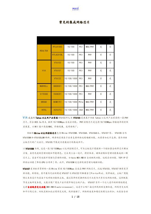
常见的集成网络芯片VIA威盛的Tahoe以太网产品家族VT6103/F/L/X VT6103是隶属于VIA Tahoe以太网产品家族的一款PHY 芯片,符合802.3u规X,提供10/100Mbps自适应功能。
PHY控制芯片是支持10/100Mbps传输速率的实体层装置,以MII接口连接MAC,价格低廉,适用面极广。
VIA的Rhine以太网控制芯片包含Rhine VT6105M、VT6106H、VT6106S/L、VT6107等。
VT6105分为VT6105M和VT6105LOM两种,两者的区别在于后者支持网络远程唤醒功能,而前者如此不支持。
因为VIA 主板芯片的广泛流行,VT6105可能是目前最流行的集成网卡。
以VT6105M为例,这是一款10/100Mbps以太网控制芯片,可为主板设计商提供一个轻松整合的单芯片解决方案,具有先进的管理功能和节能特色。
它采用三合一设计,将实体层、媒体控制和管理功能集成到一颗芯片上。
具备可有效提升侦错与管理的功能,如Auto MDI/MDIX自动跳线功能、远程启动功能、TCP/IP资料验证功能〔降低CPU占用率〕等。
此外,VT6105M还支持电源管理与唤醒功能。
VT6107是VIA非常新的一款Rhine家族10/100Mbps自适应PHY网络芯片,比起VT6103,VT6107拥有更多新功能,新特性,其中最为突出的便是VT6107与VT6122针脚兼容〔Pin-to-Pin),简单地说,主板厂商能够让本来设计为具备千兆网络功能的主板,通过简单的更换网络芯片而变为只有百兆网络功能,这样既能节省主板研发本钱,又能方便厂商生产出不同市场定位的产品。
VT6107另外一个让人意外的新特性便是支持自动线序交叉功能(MDI/MDIX auto-crossover),这是什么呢?接过网线的朋友都知道,网线有交叉线和平行线之分,双机互联如此必须用交叉线,线序接错了,网络的速度和稳定性便大打折扣。
华为交换机VRP版本升级Log
VRP升级,以S3928P为例,分两部分,bootrom的升级与flash的升级,具体软硬件需求见版本说明Starting......************************************************************ ** Quidway S3928P-PWR-EI BOOTROM, Version 323 ** ************************************************************Copyright (c) 1998-2007 Huawei Technologies Co., Ltd.Creation date : Jun 22 2007, 14:20:41CPU type : BCM4704CPU Clock Speed : 200MHzBUS Clock Speed : 33MHzMemory Size : 64MBMac Address : 00e0fc79774dPress Ctrl-B to enter Boot Menu (1)password:BOOT MENU1. Download application file to flash2. Select application file to boot3. Display all files in flash5. Modify bootrom password6. Enter bootrom upgrade menu7. Skip current configuration file8. Set bootrom password recovery9. Set switch startup mode0. RebootEnter your choice(0-9): 6Bootrom update menu:1. Set TFTP protocol parameters2. Set FTP protocol parameters3. Set XMODEM protocol parameters0. Return to boot menuEnter your choice(0-3): 1Load File name :S3900_V323.btm S3900_V513.btmSwitch IP address :10.1.1.1Server IP address :10.1.1.2Are you sure you want to update your bootrom? Yes or No [Y/N] y Attached TCP/IP interface to netdrv0.Attaching network interface lo0...done. Loading.........................................................................................................done Bootrom updating..........done!BOOT MENU1. Download application file to flash2. Select application file to boot3. Display all files in flash5. Modify bootrom password6. Enter bootrom upgrade menu7. Skip current configuration file8. Set bootrom password recovery9. Set switch startup mode0. RebootEnter your choice(0-9): 11. Set TFTP protocol parameters2. Set FTP protocol parameters3. Set XMODEM protocol parameters0. Return to boot menuEnter your choice(0-3): 1Load File name :S3900_V513.btm S3900EI-VRP310-R1602P06-S168.binSwitch IP address :10.1.1.1Server IP address :10.1.1.2Are you sure you want to download file to flash? Yes or No [Y/N] y Loading........................................................................................................................................................................... ........................................................................................................................................................................................ ........................................................................................................................................................................................ ........................................................................................................................................................................................ ........................................................................................................................................................................................ ........................................................................................................................................................................................ ........................................................................................................................................................................................ ........................................................................................................................................................................................ ....................................................doneFree flash Space: 4773888 bytesWritingflash................................................................................................................................................................................ ..............................................................................................................done!Please input the file attribute (main/backup/none):mainThe attribute of s3900EI-vrp310-r0022-224.bin is changed from main to none!done!BOOT MENU1. Download application file to flash2. Select application file to boot3. Display all files in flash4. Delete file from flash5. Modify bootrom password6. Enter bootrom upgrade menu7. Skip current configuration file8. Set bootrom password recovery9. Set switch startup mode0. RebootEnter your choice(0-9): 0Starting......************************************************************ ** Quidway S3928P-PWR-EI BOOTROM, Version 513 ** ************************************************************Copyright (c) 1998-2008 Huawei Technologies Co., Ltd.Creation date : Apr 2 2008, 16:17:35CPU Clock Speed : 200M HzBUS Clock Speed : 33MHzMemory Size : 64MBMac Address : 00e0fc79774dPress Ctrl-B to enter Boot Menu 0Auto-booting...Decompress Image.............................................................................................................................................................................. ........................................................................................................................................................................................ ...............................................................................................OK!Starting at 0x80100000...User interface aux0 is available.Press ENTER to get started.<Quidway>。
TDA7850-V8版(含BA3121)车载HIFI四声道功放模块产品规格书

二、剑飞电子车载四声道系列产品一览表
序 版本号
号
发行
前级隔 前级放 电位
颜色 PCB 尺寸
目前状态
年份
离模块 大模块 器
1 TDA7850-V1 2005 白色
/
否
2 TDA7850-V2 2007 蓝色
/
否
3 TDA7850-V3 2008 红色 78*48mm 否
电信无线猫产品大全

中国电信针对家庭adsl宽带用户,主推了“我的e家”品牌(英文名称“ONE HOME”),整合了adsl 上网、互联星空、IPTV等功能,并有免固话月租、送电话费、多帐号同时上网等“优惠”。
同时电信也与华为、中兴和上海贝尔等多家知名企业合作,定制了集无线路由器、无线AP、有线交换机、adsl猫等功能为一体的产品,以免费赠送、租赁或出售等方式交予用户使用。
此类设备上一般都有“我的e家”字样。
同时针对商业用户,电信也推出了功能更强的商务订制产品----“商务领航”或“商务宽带”。
出于自身利益的考虑,电信除了要求厂家在这些产品上印上电信指定的标识外,还要求厂家在设备出厂时进行一些修改,有的是屏蔽了固件升级功能,有的屏蔽了配置文件上传下载功能,有的屏蔽了MAC地址克隆功能,有的屏蔽了QoS功能等。
不同的设备被屏蔽的功能不尽相同,惟一相同的是都被屏蔽了路由拨号功能(PPPoE)。
这样用户就不能享受到多机同时上网的便利了。
除非使用电信所说的“多帐号同时上网”,就是在一条电话线路上,用同一个帐号,多台计算机自己拨号,从而达到同时上网的效果。
但是,这样是很危险的,因为电信会加倍计算用户的上网时间。
至于更细节的问题,不便在这里大书特书,有兴趣可以私下交流。
下面列出本人所使用并研究过的一些电信定制的宽带无线猫,特别是针对能否路由拨号(PPPoE)进行详细描述,仅供参考。
01、华为 Echolife HG520s B010版(天线在左边)除一般功能外,还拥有如IP路由、VLAN绑定、QoS等独到功能。
早期的B010版可以通过调用隐藏页面来使用PPPoE拨号,现在可以直接升级固件来使用全部功能。
B010版的HG520s的CPU为DA4-9431-PCA (此芯片为华为定制),Switch为ADM6996M,FLASH 4MB,内存为双片共16MB。
无线芯片采用的是ISL 3886IKZ系列。
02、华为 Echolife HG520s B013/B015/B016版(天线在右边)B013/B015都可以通过升级固件的方式来打开更多的功能,包括PPPoE,但B015版的升级要麻烦许多,因为在其设置界面上根本找不到升级界面,原先只能拆机用数据线等强制升级,现在虽然可以不拆机“软升”,但过程也很复杂。
CBM培训资料

Engineer ITControl Builder MVersion 3.2Getting Started工业工程IT控制应用开发版本 3.2入门山东恒拓科技开展本资料是由山东恒拓科技开展〔ABB系统集成商〕内部员工参考CBM原版说明书翻译整理而成,本书主要用于内部参考学习及客户培训使用,未经山东恒拓科技开展许可的前提下,其他任何人员不可擅自复制,传播。
译者:孔祥玉。
本文献中的所有信息可能会在没有通知的前提下发生修改,并且ABB拥有对所有信息的解释权。
对于本文献中可能出现的任何错误,ABB不负任何法律责任。
在本文献的使用过程中,ABB对于因自然或非自然因素而产生的直接的、间接的、特殊的和附带的所有损失不负任何责任,且ABB对本文献中软件和硬件的描述中产生的任何损失不负任何责任。
在没有ABB的许可之下,本文献或其中的章节不可进行复制,且其中内容不可授予第三方或任何未授权的应用。
版权拥有© 1999 ABB保存所有版权发行:2002年12月文献编号:3BSE 028 807 R201 Rev B商标本文中使用到的注册和商标:Windows 微软公司注册ActiveX 微软公司注册PostScript Adobe Systems Inc. 注册Acrobat Reader Adobe Systems Inc. 注册Industrial IT ABB 注册第一部Control Builder M目录关于本书简介 (6)第一章–介绍Control Builder M产品总览........................................................................ ... ... . (7)编程语言....................................................... ... ... ... ... ... . (7)工程开发器.................................................... ... . (7)库................................ ... ... (8)安装要求....................................................................... ....................... . (8)可以支持的控制器组态.......... .. ....................................... ....................... . (9)Control Builder和控制器组态................................................. (10)分散控制................ ....... ....... ....... ....... ....... ........................... ..................... .. (11)Control Builder现有版本及其差异........................................ (12)第二章–安装Control Builder M................ ..... ..... ..... ..... .. .. ... .. (13)逐步安装指南........................................................ .. .. ... (14)TCP/IP 网络协议................................................. ..... ..... ..... .. (14)设置...................................................................................... ...... ...... ...... .. (15)启动................... ..... ..... ..... ..... . (15)AC800M/C的MMS效劳器............................................................. . (15)添加删除程序...................... ..... ..... ..... .. (15)第三章–培训导言.............................. ..... ..... ..... .. (17)开始新工程.......................................... ......... ......... (17)工程开发器...................................................................... . (18)标题菜单工具 (36)库...................................................................................................................... .. (37)控制器.................................................................................................................... . 38 任务. (40)应用 (40)变量间接 (43)变量声明〔定义〕 (43)局部变量 (44)模拟 (47)关闭Control Builder M (49)第四章–举例– Shop Doors简介 (51)选择模板 (52)声明变量和数据类型 (53)变量声明 (54)使用ST语言编写代码 (56)改变编程语言 (56)声明功能块 (57)划分程序功能段 (58)代码输入 (59)模拟 (62)硬件组态 (64)连接I/O通道和应用 (65)第五章–下装和测试简介 (71)通过串行电缆进行操作系统下装 (71)给冗余控制器下装操作系统 (73)设定IP地址 (74)通过以太网下装工程 (77)在线测试 (91)附录AC800 M/C的OPC效劳器简介 (91)自动启动OPC效劳器OPC的组态面板第二部AC800M Controller Hardware目录关于本书第一章–简介产品总览 (27)AC 800M 控制器的突出特性 (38)第二章–安装安装环境要求 (41)电缆 (43)电源 (44)防护等级 (46)将AC 800M单元安装于标准DIN-Rail导轨 (47)安装PM856/860/861/TP830 控制器单元〔单独〕 (54)安装PM861/TP830 控制器单元〔冗余〕 (62)安装PROFIBUS DP 通讯单元,CI851/TP851 (65)安装RS232-C通讯单元, CI853/TP853 (69)安装PROFIBUS DP-V1通讯单元, CI854/TP854 (70)安装CEX-bus电缆 (74)安装ModuleBus 电缆 (75)安装SD82x 供电电源 (76)安装主断路器 (77)安装SS822冗余电源选择模块 (79)安装SB821外部电池 (83)安装I/O 单元 (83)柜体安装 (84)第三章–组态简介 (89)连接到Control Builder M (89)连接到控制网 (90)通讯方式 (91)控制器IP地址 (93)在Control Builder M设置冗余控制器 (93)I/O系统 (94)驱动系统 (98)供电系统 (100)柜体中的电源模块 (101)柜外电源设备Powering Field Equipment outside the Cabinet (101)外部+24 V DC 电源 (103)第四章–操作AC 800M 控制器(PM856/860/861) (107)启动 (110)启动模式 (110)自动切换到冗余后备控制器 (112)AC 800M系统运行检查 (113)观察单控制器的运行 (113)观察冗余控制器的运行 (115)第五章–维修维修频率 (117)更换电池 (118)内部电池 (118)SB821外部电池单元 (120)在线插拔 (124)更换PM861冗余控制器 (124)维修步骤 (125)查找问题 (126)PM856/860/861控制器单元 (126)PM861 CPU冗余单元 (127)内部电池/ SB821外部电池 (127)PROFIBUS DP – CI851 (128)RS232-C Channels – CI853 (132)PROFIBUS DP-V1 – CI854 (133)Table of Contents附录–硬件单元PM856/PM860和TP830 –控制器单元 (137)技术数据 (138)性能数据 (142)PM861 and TP830 –控制器单元 (143)技术数据 (144)性能数据 (146)CI851 和TP851 – PROFIBUS DP单元 (147)CI853 和TP853 – RS232-C单元 (155)CI854 和TP854 – PROFIBUS DP-V1 Interface (159)电源单元–SD821, SD822 和SD823 (175)SS822 – (冗余电源选择单元) (183)SB821外部电池 (187)其他 (189)TB850 -- CEX-bus终端电阻 (189)TB851 -- CEX-bus终端电阻 (190)TB807 ModuleBus终端电阻 (191)TB852 RCU 连接终端电阻 (191)TK850 CEX-bus 外部电缆 (191)TK851 RCU连接电缆 (191)TK853电缆 (192)TK212工具电缆 (193)第一部Control Builder M关于本书简介欢迎使用本软件〔Control IT for AC 800M/C〕----一个真正全开放的工业控制开发系统。
光纤收发器光通信产品简单介绍

输媒体转换单位。 ❖ 订购信息示例:10/100M 单模双纤 1310nm 20KM SC接口 外置电源
AC220V (备注:电源类型 包装要求 运输方式)
产品规格对应表
10/100M Auto-sensing fiber media converterv dual fiber (external power supply) 10/100M 自适应,多模,单模双纤,外置电源 5V1A
10/100/1000M single Bi-Di fiber media converter (ExternalPower Supply) 10/100/1000M 自适应,单纤双向-WDM,外置电源 5V2A
10/100/1000M, MM,2km, SC connector,1310/1550nm 多模单纤 10/100/1000M, SM,20km, SC connector, 1310/1550nm 10/100/1000M, SM,40km, SC connector, 1310/1550(FP)nm 35km内 10/100/1000M, SM,40km, SC connector, 1310/1550(DFB)nm 10/100/1000M, SM60km, SC connector, 1310/1550(DFB)nm 10/100/1000M, SM,80km, SC connector, 1490(DFB)/1550(DFB)nm
徐开旺光纤通信产品知识讲座
光纤收发器(Media converter)
一、分类(按结构分): 1.外置光纤收发器 (电源外置) external power supply 2.内置光纤收发器 internal power supply 3.插卡式光纤收发器 Media Converter Card Type 4收发器用户卡 5.机架式光纤收发器 (14槽机架和16槽机架) 14-Slot Media Converter Chassis
RTL8306SD(M)应用参考电路原理图
PHY2PTXD2 PHY2PTXD1 PHY2PTXD0 PHY2PTXEN PHY2PTXC PHY2PRXC PHY2PRXDV
PHY2PRXD3 PHY2PRXD2 PHY2PRXD1 SDA_MDIO SCL_MDC PHY2PRXD0
MRXD3_PTXD3 MRXD2_PTXD2
ENDEFER PHY2PCOL PHY2PTXD3
P4LNKSTA# (5,6) P4LNKSTA# P4SPDSTA (5,6) P4SPDSTA P4DUPSTA_HMPGCRS (5,6) P4DUPSTA_HMPGCRS P4FLCTRL_CPUINT# (5,6) P4FLCTRL_CPUINT#
MAC4 MII Stapping
(5,6) DISDUALMII (5,6) P4MODE1 (5,6) P4MODE0 (5,6) GXMODE (3,5,6) DUP3_GYMODE
MRXC_PTXC MRXDV_PTXEN MRXD3_PTXD3 MRXD2_PTXD2 MRXD1_PTXD1 MRXD0_PTXD0 MCOL_PCOL MTXC_PRXC MTXEN_PRXDV MTXD3_PRXD3 MTXD2_PRXD2 MTXD1_PRXD1 MTXD0_PRXD0
MAC4 MII Interface
EEPROM
1.1
D
MAC5 MII
RTL8306S/SD/SDM Power Consumption Table
Power supply 1.8V 3.3V Max Current (mA) 550 mA 130 mA Max Total Power Consumption : 1386mW
D
MAC5
江森DDC模块配置

1 x XT-9100-8304通讯模块
1 x XP-9102-8304 6AI 2AO模块
1 x XP-9104-8304 4DI 4DO模块
带继电器座
6AI, 4DI, 2AO, 4DO
EP-1MX33-100-00
1 x XT-9100-8304通讯模块
2 x XP-9103-8304 8DO模块
江森ADS系列DDC配置
E-Panel
EP-11501-100-00
FX15控制器(N2 Bus,带电源,继电器座)
6AI, 8DI, 4AO, 8DO
EP-11551-100-00
FX15控制器(N2 Bus,带电源,显示,继电器座)
6AI, 8DI, 4AO, 8DO
EP-11502-100-00
DX9100-8454
8AI, 8DI, 8AO, 6DO
DC-F20000-010-00
DDC控制盘(尺寸:700 x 500)
1x XP9104
4DI, 4DO
DC-L20000-010-00
DDC控制盘(尺寸:700 x 500)
2x XP9103
8DO
DC-N20000-010-00
DDC控制盘(尺寸:700 x 500)
FX15控制器(LON Bus,带电源,继电器座)
6AI, 8DI, 4AO, 8DO
EP-11552-100-00
FX15控制器(LON Bus,带电源,显示,继电器座)
6AI, 8DI, 4AO, 8DO
EP-1MX20-000-00
1 x XT-9100-8ห้องสมุดไป่ตู้04通讯模块
- 1、下载文档前请自行甄别文档内容的完整性,平台不提供额外的编辑、内容补充、找答案等附加服务。
- 2、"仅部分预览"的文档,不可在线预览部分如存在完整性等问题,可反馈申请退款(可完整预览的文档不适用该条件!)。
- 3、如文档侵犯您的权益,请联系客服反馈,我们会尽快为您处理(人工客服工作时间:9:00-18:30)。
RTL8306E/8306M/8304EPROGRAMMING GUIDEV1.0.2Feb 2, 2012No. 2, Innovation Road II, Hsinchu Science Park, Hsinchu 300, TaiwanTel.: +886-3-578-0211. Fax: +886-3-577-60471Rev. 1.0.22Rev. 1.0.2COPYRIGHT©2012 Realtek Semiconductor Corp. All rights reserved. No part of this document may be reproduced, transmitted, transcribed, stored in a retrieval system, or translated into any language in any form or by any means without the written permission of Realtek Semiconductor Corp.TRADEMARKSRealtek is a trademark of Realtek Semiconductor Corporation. Other names mentioned in this document are trademarks/registered trademarks of their respective owners.DISCLAIMERRealtek provides this document “as is”, without warranty of any kind, neither expressed nor implied, including, but not limited to, the particular purpose. Realtek may make improvements and/or changes in this document or in the product described in this document at any time. This document could include technical inaccuracies or typographical errors.USING THIS DOCUMENTThis document is intended to be used by the software engineer when programming for Realtek RTL8306E controller chips. Though every effort has been made to assure that this document is current and accurate, more information may have become available subsequent to the production of this guide. In that event, please contact your Realtek representative for additional information that may help in the development process.CONFIDENTIALITYThis document is confidential and should not be provided to a third-party without the permission of Realtek Semiconductor Corporation.REVISION HISTORY3Rev. 1.0.24Rev. 1.0.2Table of Contents1 OVERVIEW (6)2 DIRECTORY STRUCTURE (7)3 ASIC DRIVER (8)3.1 P ORTING ISSUE (8)3.2 I NITIALIZA TION (9)3.3 C HIP MODULE (9)4 RTK API FOR RTL8306E (12)4.1 VLAN (12)4.2 VLAN T RANSLATION (17)4.3 Q-IN -Q (19)4.4 L OOKUP TABLE (22)4.5 QOS (26)4.6 CPU PORT (31)4.7 MIB (33)4.8 P HY (35)4.9 F ORCE E XTERNAL I NTERFACE (38)4.10 D OT 1X (43)4.11 P ORT MIRROR (47)4.12 P ORT I SOLA TION (48)4.13 MAC L EARNING L IMIT (49)4.14 ACL (50)4.15 M ISC (52)5 IGMP SNOOPING/MLD SNOOPING (54)5.1 G ENERAL DESCRIPTION (54)5.2 IGMP S NOOPING V ERSION 1 (55)5.2.1 IGMP Snooping porting guide (55)5.2.2 IGMP snooping function usage guide: (56)5.2.3 Advanced issues: (58)5.3 IGMP/MLD S NOOPING V ERSION 2 (59)5.3.1 Multicast Snooping porting guide (59)5.3.2 Multicast snooping function usage guide: (60)6 APPLICATION (63)6.1 XDSL (63)6.2 EPON ONU (65)7 PORT NUMBER (70)7.1 E XTENSION PORTS (70)7.2 P ORT MAPPING (70)5Rev. 1.0.2REALTEK SEMICONDUCTOR CORP (71)HEADQUARTERS (71)6Rev. 1.0.21 OverviewThe RTL8306E release package contains ASIC drivers, which provides general APIs that based on user configuration to configure relative ASIC registers. Inside of the ASIC driver, it uses GPIO to emulate MDC/MDIO signal to communicate with RTL8306E. This part needs to be porting to the target platform. The RTL8306E release package can also be applied to other chips, such as RTL8304E/RTL8306M. These ASICs may have different port numbers. For example RTL8304E only have 4 ports, but RTL8306E have 6 ports. The port number descriptions for different ASICs can be found in chapter 7.This SDK API programming guide file uses RTL8306E as an example to descript the usage of API functions. But for different ASICs, the port parameter which is needed by some API fu nction is different from RTL8306E , due to the AISCs ’ different port numbers. So in order to us e ASIC driver code, it ’s recommended for you to make clear of the ASIC ’s port number at first. And then make some configuration code modification based on the descriptions of sector 3.3 an d chapter 7.2 Directory StructureRTL8306E release package is distributed with the following files:7Rev. 1.0.23 ASIC Driver3.1 Porting issueRTL8306E management interface is MDC/MDIO, MDC is clock and MDIO transmits data. The source code using two GPIO pins to emulate MDC/MDIO signals. Porting this driver to customer platform needs to modify files mdcmdio.c and mdcmdio.h. In these files, there are two kinds of realization, one is realized by calling GPIO API, the other is by configuring CPUGPIO register directly, any one of them is ok. If you want to write your own MDC/MDIO code, you should follow these steps: Firstly, choose two GPIO pins, specify one as MDC, the other as MDIO;Secondly, rewrite functions _smiZbit, _smiReadBit, _smiWriteBit, these are local functions._smiZbit sets two pins low to simulate HiZ state. _smiReadBit generates 1 -> 0 transition and sampled at 1 to 0 transition time, thus read one bit from MDC/MDIO interface. _smiWriteBit generates 0 -> 1 transition and put data ready during 0 to 1 whole period, it write one bit into the interface. Between MDC 1 and 0 transition, proper delay should be added, delay time will affects the interface accessing speed, the less delay, the higher speed. In IEEE 802.3 standard, it says that MDC is an aperiodic signal that has no maximum high or low times, but minimum high and low times for MDC shall be 160 ns each, and the minimum period for MDC shall be 400 ns. Please obey this limitation.Thirdly,smiRead and smiWrite need almost no modification, smiRead reads one PHY register content, smiWrite writes value into PHY register, both of them are global functions.You should pay attention to another issue that is to prevent CPU from being interrupted by IRQ during smi read and write, so in smiRead and smiWrite, CPU interrupt should be disabled before smi operation and be enabled after smi operation. We use rtlglue_drvMutexLock() andrtlglue_drvMutexUnlock() which are based on RTL865X platform to realize that, if using other platform, please rewrite it.8Rev. 1.0.23.2 InitializationThe system must be properly initialized, following figure shows a complete initialization, please pay attention to sequence of it. If you do not use the module, the module need not be initialized.After rtk_switch_init, rtk_qos_init should be firstly called, then rtk_cpu_enable_set andrtk_cpu_tagPort_set. rtk_qos_init is to configure port Tx queue numbers, it could support 4 queues at most, default only one queue. Multi-queues have different priority, higher queue could share more bandwidth of the port, thus port could be differentiated maximum four flows. rtk_cpu_tagPort_set is to specify which port is CPU port and the CPU tag insert mode.Fig. 3-1 Initialization3.3 Chip moduleThe ASIC driver supports multiple Realtek switch ASIC family. Users should define one of the following flags in the file “rtl8306e_asictypes.h” depending on the ASIC which you use. Then the API driver for the ASIC would be compiled and linked into your program. Those code segments forun-supported chip would not be complied and linked, and will not increase your program size.⏹CHIP_RTL8306E⏹CHIP_RTL8306M⏹CHIP_RTL8304EBefore using the driver code, you have to define one of the above flags depend on the type of the9Rev. 1.0.210Rev. 1.0.2 ASIC you used. When you use the API functions which need port number as input parameter, you are only permitted to use the port macro definitions corresponded to the flag. When using the API functions which need port mask as input parameters, you are recommended to use a macro to translate these ASIC ’s port mask value to the API ’s port mask value. After using the API functions which return port mask as output parameters, you are recommended to use a macro to translate these output parameters to ASIC ’s port mask value. Only RTL8306E and RTL8306M are permitted to use Arabic numerals as port and port mask, and it ’s not needed to use macro to do the port mask value translation. The port macros and port mask translation macro are defined in “rtl8306e_asictypes.h ”.The port macro and port mask translation macro definitions corresponded to the dedicated flag are listed as follows:(1) CHIP_RTL8306E:RTL8306E_PORT0RTL8306E_PORT1RTL8306E_PORT2RTL8306E_PORT3RTL8306E_PORT4RTL8306E_PORT5(2) CHIP_RTL8306M:RTL8306M_PORT0RTL8306M_PORT1RTL8306M_PORT2RTL8306M_PORT3RTL8306M_PORT4RTL8306M_PORT5 (3) CHIP_RTL8304E:RTL8304E_PORT0RTL8304E_PORT1RTL8304E_PORT2RTL8304E_PORT3RTL8304E_PORTMASKIN(x) RTL8304E_PORTMASKOUT(x) For example, if you use ASIC RTL8304E which have only 4 ports (port0~1 and external port 0~1, for detail please see chapter 7), so before to use the driver code, first “rtl8306e_asictypes.h ” should be included in your code files. You have to define macro CHIP_RTL8304E in “rtl8306e_asictypes.h ”, and then you are only permitted to use port macros for RTL8304E as the port parameter of the API function.11Rev. 1.0.2For example, if you want to call API function:rtk_api_ret_t rtk_cpu_tagPort_set(rtk_port_t port, rtk_cpu_insert_t mode) You are only permitted to use RTL8304E_PORT0, RTL8304E_PORT1, RTL8304E_PORT2 or RTL8304E_PORT3 as port parameter for this API function.If you want to call API function which use port mask as input parameters as follows:rtk_api_ret_t rtk_vlan_set(rtk_vlan_t vid, rtk_portmask_t mbrmsk, rtk_portmask_t untagmsk, rtk_fid_t fid)mbrmsk and untagmsk are input parameters which are also port mask. If the vlan entry you want to set has vid = 2, fid = 0, member port set = port0 and port2, and untag member port set = port0 and port3. So:vid = 2;fid = 0; mbrmsk = 0x5; /*port 0 and port 2*/untagmsk = 0x9; /*port 0 and port 3*/mbrmsk = RTL8304E_PORTMASKIN (mbrmsk );untagmsk= RTL8304E_PORTMASKIN (untagmsk ).rtk_vlan_set(vid, mbrmsk, untagmsk, fid); Then you can call rtk_vlan_set() using mbrmsk and untagmsk as input parameters now.If you want to call API function which use port mask as output parameters as follows:rtk_api_ret_t rtk_vlan_get(rtk_vlan_t vid, rtk_portmask_t *pMbrmsk,rtk_portmask_t *pUntagmsk, rtk_fid_t *pFid)*pMbrmsk and *pUntagms are output parameters which are also port mask returned by this API. After call rtk_vlan_get() and you will get *pMbrmsk and *pUntagm . Before using them directly, you have to call macro RTL8304E_PORTMASKOUT(x) to translate them into ASIC ’s port mask values corresponded to RTL8304E. You have to call:*pMbrms = RTL8304E_PORTMASKOUT (*pMbrms ).* pUntagms = RTL8304E_PORTMASKOUT (*pUntagms ).Then you can use *pMbrmsk and *pUntagms as normal RTL8304E port mask variables now.12Rev. 1.0.24 RTK API for RTL8306E4.1 VLANRTL8306E supports 16 VLANs. After the switch resets, it is dumb mode, the VLAN function is disabled as the default configuration. User should use API rtk_vlan_init to initialize the VLAN before using VLAN. The initialization will enable VLAN function and set up a default VLAN with VID 1 that contains all ports. Moreover, each port’s PVID will also be set to default VLAN .After initialization, user can add and set VLAN 1~4094 through API rtk_vlan_set, configure itsmember set and untag set. In order to get the information of member set and untag set on specified VLAN, rtk_vlan_get could be used . For Port-Based VLAN, there are two APIs rtk_vlan_portPvid_set and rtk_vlan_portPvid_get provided to set and get the PVID of the ports.User can also turn on ingress filter function through rtk_vlan_portIgrFilterEnable_set and accept frame type function through rtk_vlan_portAcceptFrameType_se t.Here are explanations and example codes for VLAN APIs. The example codes ignore the error check.rtk_api_ret_t rtk_vlan_init(void)This function enables VLAN and gives the default configuration, and it should be called before using VLAN. It will clear the VLAN table and set up a default VLAN with VID 1 that contains all ports. It also sets each port’s PVID to the default VLAN . After VLAN initialization, it will be set tag aware, the switch uses tagged-VID VLAN mapping for tagged frames while using Port-Based VLAN mapping for untagged frames. After invocating rtk_vlan_init , user can change the default VLAN configuration through the following introduced API rtk_vlan_set and rtk_vlan_portPvid_set .Example:/* initialize VLAN */rtk_vlan_init ();/* all the ports are in the default VLAN 1 after VLAN initialized, modify it as followsVLAN1 member: port0, port1, port2;VLAN2 member: port3, port4, port5 */rtk_portmask_t mbrmsk, untagmsk;mbrmsk.bits[0]=0x07;untagmsk.bits[0]=0x3F;rtk_vlan_set(1, mbrmsk, untagmsk, 0);mbrmsk.bits[0]=0x38;untagmsk.bits[0]=0x3F;rtk_vlan_set(2, mbrmsk, untagmsk, 0);/* set PVID for each port */13Rev. 1.0.2rtk_vlan_portPvid_set(0, 1, 0);rtk_vlan_portPvid_set(1, 1, 0);rtk_vlan_portPvid_set(2, 1, 0);rtk_vlan_portPvid_set(3, 2, 0);rtk_vlan_portPvid_set(4, 2, 0);rtk_vlan_portPvid_set(5, 2, 0);rtk_api_ret_t rtk_vlan_set(rtk_vlan_t vid, rtk_portmask_t mbrmsk, rtk_portmask_t untagmsk, rtk_fid_t fid)typedef uint32 rtk_vlan_t;typedef struct rtk_portmask_s{uint32 bits[RTK_TOTAL_NUM_OF_WORD_FOR_1BIT_PORT_LIST];} rtk_portmask_t;typedef uint32 rtk_fid_t;User could configure the member set and untag set for specified VLAN through this API. The VID should be 1~4094. The mbrmask ’s bit N means port N. For example, mbrmask.bits[0] = 23=0x17=0b010111 means port 0,1,2,4 in the member set. The input parameter untagmsk is used to configure untag set for specified VLAN, which means if the untagmsk bit value is 1, the packets egress form the corresponding port will be removed VALN tag. The input parameter fid is for SVL/IVL usage, 8306E only supports SVL, so fid is no usage and can be any value.Example:/* set port 0,1,2,3 as member set and port 2,3 as untag set to VLAN 1000 */rtk_vlan_t vid;rtk_portmask_t mbrmsk, untagmsk;rtk_fid_t fid;vid = 1000;mbrmsk.bits[0]=0x0F;untagmsk.bits[0]=0x0C;fid = 0;rtk_vlan_set(vid, mbrmsk, untagmsk, fid);rtk_api_ret_t rtk_vlan_get(rtk_vlan_t vid, rtk_portmask_t *pMbrmsk, rtk_portmask_t *pUntagmsk, rtk_fid_t *pFid)typedef uint32 rtk_vlan_t;typedef struct rtk_portmask_s{uint32 bits[RTK_TOTAL_NUM_OF_WORD_FOR_1BIT_PORT_LIST];} rtk_portmask_t;typedef uint32 rtk_fid_t;The API can get the information of member set, untagged set, and filtering database on the specified14Rev. 1.0.2VLAN. The information is retrieved in mbrmask. The mbrmask ’s bit N means port N. For example, mbrmask.bits[0] = 23=0x17=0b010111 means port 0,1,2,4 in the member set. 8306E only supports SVL, so the pFid value retrieved is meaningless.Example:/* get the member set and untagged set on VLAN 1000 */rtk_vlan_t vid;rtk_portmask_t mbrmsk, untagmsk;rtk_fid_t fid;vid = 1000;rtk_vlan_get(vid, &mbrmsk, & untagmsk, &fid);rtk_api_ret_t rtk_vlan_portPvid_set(rtk_port_t port, rtk_vlan_t pvid, rtk_pri_t priority)Set each port’s PVID and 802.1Q based default priority for the port. The specified priority will only be assigned to the untagged frame and then system can map the untagged frame to the proper output queue for 802.1Q-based QoS. Just specify the priority to 0 if you don’t turn on the QoS or use other QoS mechanisms instead of 802.1Q-based. Before using the API, user should call rtk_vlan_set to set the member set and untag set for the VLAN first.Example:/* set port0, port1 as member set to VLAN 2000 */rtk_vlan_t vid;rtk_portmask_t mbrmsk, untagmsk;rtk_fid_t fid;vid = 2000;mbrmsk.bits[0]=0x03;untagmsk.bits[0]=0;fid = 0;rtk_vlan_set(vid, mbrmsk, untagmsk, fid);/* set PVID of port 0/1 to 2000 and 802.1Q based default priority to 0*/rtk_vlan_portPvid_set(0, 2000, 0);rtk_vlan_portPvid_set(1,2000, 0);rtk_api_ret_t rtk_vlan_portPvid_get(rtk_port_t port, rtk_vlan_t *pPvid, rtk_pri_t *pPriority)Get each port’s PVID and 802.1Q based default priority for the port.Example:/* get PVID and 802.1Q based default priority of port1 */rtk_vlan_t vid;rtk_pri_t priority;15Rev. 1.0.2rtk_vlan_portPvid_get(1, &vid, &priority);rtk_api_ret_t rtk_vlan_portAcceptFrameType_set(rtk_port_t port,rtk_vlan_acceptFrameType_t accept_frame_type)Acceptable frame type could be set for each port, and priority-tagged packet (VID = 0) is treated as untagged packet.Example:/* port 0: accept tagged and un-tagged packet,*//* port 1: accept only tagged packet,*//* port 2: accept only un-tagged packet.*/rtk_vlan_portAcceptFrameType_set (0, ACCEPT_FRAME_TYPE_ALL);rtk_vlan_portAcceptFrameType_set (1, ACCEPT_FRAME_TYPE_TAG_ONLY);rtk_vlan_portAcceptFrameType_set (2, ACCEPT_FRAME_TYPE_UNTAG_ONLY);rtk_api_ret_t rtk_vlan_portAcceptFrameType_get(rtk_port_t port,rtk_vlan_acceptFrameType_t *pAccept_frame_type)Get the acceptable frame type of the port.Example:/* get acceptable frame type of port 0 */rtk_vlan_acceptFrameType_t acceptFrameType;rtk_vlan_portAcceptFrameType_get (0, &acceptFrameType);rtk_api_ret_t rtk_vlan_destroy(rtk_vlan_t vid)Delete an existed VLAN, which means its VID, port member set and untagged set in VALN table all will be set to 0. If the VLAN does not exist, it returns RT_ERR_VLAN_ENTRY_NOT_FOUND. Example:/* delete the VLAN whose VID is 2007 */rtk_vlan_destroy(2007);rtk_api_ret_t rtk_vlan_portIgrFilterEnable_set (rtk_port_t port, rtk_enable_t igr_filter)Set VLAN ingress for each port. RTL8306E use one ingress filter for whole system, not for each port, so any port you set will affect all ports ingress filter setting. While VLAN function is enabled, ASIC will decide VLAN ID for each received frame and get belonged member ports from VLAN table. If the ingress port is not included in VLAN member ports, ASIC will drop received frame if VLAN ingress function is enabled.Example:16Rev. 1.0.2/*Enable the VLAN ingress filter function for all ports*/rtk_vlan_portIgrFilterEnable_set(0, ENABLED);/*Disable the VLAN ingress filter function for all ports*/rtk_vlan_portIgrFilterEnable_set(0, DISABLED);rtk_api_ret_t rtk_vlan_vlanBasedPriority_set(rtk_vlan_t vid, rtk_pri_t priority)For 8306E, each VLAN could be assigned a priority, which means the VLAN ID from IEEE802.1Q VLAN tag can be mapped to a 2-bit priority. This API will enable VID based priority function for the specified VID and set VID-to-priority mapping.Example:/*Set priority 2 for VID 100*/rtk_vlan_t vid;rtk_pri_t priority ;vid = 100;priority = RTL8306_PRIO2;rtk_vlan_vlanBasedPriority_set(vid, priority);int32 rtl8306e_vlan_tagInsert_set(uint32 egPort, uint32 igPortMsk)The RTL8306E can insert VLAN tag with the ingress port ’s PVID for untagged packets if the egress port’s insert tag mask register setting is enable for the ingress port. egPort is packet egress port, if the packet is untagged and its ingress port is in the igPortMsk , it will be inserted with a VLAN tag. But if ingress packet already has a VALN tag or its ingress port is not in the igPortMsk ,then VALN tag will not be inserted.Example:/*set the packets ingress from port1/3/5 to be inserted a VALN tag when they are transmitted out of port0 */rtl8306e_vlan_tagInsert_set(0, 0x2A);17Rev. 1.0.24.2 VLAN TranslationThe RTL8306E supports VLAN translation feature. With the VID-to-VID mapping in each VLAN entry, the RTL8306E can translate the VLAN IDs from private networks into those used in the service providers' network, and vice verse. The UNI (User-Network Interface) is the interface to the customer s’ private network and the NNI (Network-Network Interface) is the interface to the service providers'network. Each port of the RTL8306E can be and must be configured as NNI or UNI in VLAN translation application. The VLAN translation can take effect only when the traffic passes across these two kinds of interface. There will be no tag change to the packets which are transmitted from NNI to NNI or from UNI to UNI.Here are explanations and example codes for VLAN translation API. The example codes ignore the error check.rtk_api_ret_t rtk_vlan_vidTranslationEnable_set(rtk_enable_t enable, rtk_portmask_t nniMask)This function sets vlan translation function enabled or disabled, and decides which port is NNI port or UNI port. In nniMask , bit n means port n, and bit value 1 means the port is NNI port, 0 means the port is UNI portExample:/*Enable VLAN translation,*//*UNI port: port0, port1, port2, port3;*//*NNI port: port4, port5 */rtk_vlan_vidTranslationEnable_set (ENABLED, 0x30);rtk_api_ret_t rtk_vlan_vidTranslationEnable_get(rtk_enable_t *pEnable,rtk_portmask_t *pNniMask)This function gets vlan translation function status (enabled or disabled), and which port is NNI port or UNI port. In nniMask , bit n means port n, and bit value 1 means the port is NNI port, 0 means the port is UNI port.Example:/*Get VLAN translation status*/rtk_enable_t enable;rtk_portmask_t nniMask;rtk_vlan_vidTranslationEnable_get (&enable, &nniMask);rtk_api_ret_t rtk_vlan_vidTranslation_set(rtk_vlan_t vid, rtk_vlan_t nvid)This API is used to translate a VID to a new VID when VLAN translation happens. The new VID will be set into the VLAN table entry and could be used by Q-in-Q or vlan translation function. Before18Rev. 1.0.2using this API, please make sure the old VID already exists in the VLAN table, otherwise it will return RT_ERR_VLAN_ENTRY_NOT_FOUND.Example:/*Suppose VID 1 already exists in VLAN table, translate VID 1 to new VID 200 */rtk_vlan_t vid, nvid ;vid = 1 ;nvid = 200 ;rtk_vlan_vidTranslation_set (vid, nvid);19Rev. 1.0.24.3 Q-in-QRTL8306E support QinQ function which allows tagging the tagged packet. The format of the double tagged packet is shown below. The Tag Protocol Identifiers (TPID) of the inner tag and the outer tag can be configured via registers. When QinQ function is enabled, the RTL8306E will always insert outer tag to the packet when the egress port is NNI and remove outer tag on UNI port. There will be no tag change to the packets which are transmitted from NNI to NNI or from UNI to UNI. The QinQ Function and VLAN translation can not be employed at the same tim e.Here are explanations and example codes for Q-in-Q API. The example codes ignore the error check.rtk_api_ret_t rtk_svlan_init(void)This API should be called before using SVLAN. It can setup some rules for SVLAN. After calling this API, all ports are set as CVLAN port. User can use rtk_svlan_servicePort_add to add SVLAN port. Example:/* initialize SVLAN */ rtk_svlan_init (); rtk_api_ret_t rtk_svlan_servicePort_add(rtk_port_t port)This API can set the port as NNI port (connected to provider switch). All frames received from this port will recognize Service VLAN Tag.Example:/* set port 5 as SVLAN service port */rtk_svlan_servicePort_add (5); rtk_api_ret_t rtk_svlan_servicePort_del(rtk_port_t port)The API is used to disable one service port in the specified deviceExample:/* delete port 5 from service port list */rtk_svlan_servicePort_del (5); rtk_api_ret_t rtk_svlan_tpidEntry_set(rtk_svlan_tpid_t svlan_tag_id)The API is used to set S-VLAN tag TPID, and the default value is 0x88a8. For example, when TPID is 0x88a8, the egress tag with VID 1 should be 88-A8-00-01.Example:/* Set TPID to 0x9100*/20Rev. 1.0.2 rtk_svlan_tpidEntry_set(0x9100);rtk_api_ret_t rtk_svlan_portPvid_set(rtk_port_t port, rtk_vlan_t pvid, rtk_pri_t priority, rtk_dei_t dei)The API is used to set port default outer tag VID(SVLAN PVID) and default outer tag priority. The input parameter is dei meaningless for 8306E.Example:/* set port0’s SVLAN PVID to 1000, default outer tag priority to 2*//* set port1’s SVLAN PVID to 2000, default outer tag priority to 3*/rtk_svlan_servicePort_add (0);rtk_svlan_servicePort_add (1);rtk_svlan_portPvid_set(0, 1000, 2, 0);rtk_svlan_portPvid_set(1, 2000, 3, 0);rtk_api_ret_t rtk_vlan_tagSrc_set(rtk_port_t port, rtk_vidSrc_t vidSrc, rtk_priSrc_t priSrc)The API could set outer tag or translated new VLAN tag vid/priority source, when Q-in-Q or VLAN translation modifies VLAN tag.vidSrc could be set following macros:RTL8306E_VIDSRC_POVID - port default outer tag VIDRTL8306E_VIDSRC_NVID - New VID got by VLAN table searchpriSrc could be set following macros:RTL8306E_PRISRC_PPRI - port default outer tag priorityRTL8306E_PRISRC_1PRMK - original VLAN tag priority or 1p remarking priority(optional) The port default outer tag VID and priority could be configured by API rtk_svlan_portPvid_set . Example:/*Set the packet transmitted out of port 2 when VLAN translation happens, its new tag VID is*//*decided by NEW VID got by VLAN table search, and priority is decided by original tag priority or*/ /*1p remarking priority.*/rtk_vlan_tagSrc_set (2, RTL8306E_VIDSRC_NVID, RTL8306E_PRISRC_1PRMK);rtk_api_ret_t rtk_vlan_tagSrc_get(rtk_port_t port, rtk_vidSrc_t *pVidSrc, rtk_priSrc_t *pPriSrc)The API could get the tag vid and priority source for Q-in-Q and VLAN translation.Example:/*Get the packets transmitted out of port 5 when VLAN translation happens, its new tag vid*//*and priority source.*/rtk_vidSrc_t vidSrc;21Rev. 1.0.2rtk_priSrc_t priSrc;rtk_vlan_tagSrc_get (5, &vidSrc, &priSrc);22Rev. 1.0.24.4 Lookup tableRTL8306E supports 2K-entry lookup table which supports 4-way hashing lookup, CPU could access lookup table through MDC/MDIO interface. Hashing function generates 9-bit lookup index which is the combination of MAC[13:15] and MAC[0:5], for each index, there are 4-entry to save the hash collision MAC address.MAC address stored in the lookup table does not have any constrain which means I/G-bit can be one or zero. When address with I/G-bit set to be zero, the address is unicast address, while I/G-bit one means multicast address.Unicast address property includes static or dynamic, authorized or unauthorized. Dynamic unicast MAC address entry is auto-learned by ASIC, and after a period of time(aging time, normal 300 second), it will be aged out and removed. Static unicast MAC address is only written by CPU throughrtk_l2_addr_add , it will exist in the lookup table all along until application use API rtk_l2_addr_del to delete it. Authorized property is also assigned by CPU, it is for IEEE 802.1x application, authorized MAC address also never age out.Multicast address is for multicast application such as IP multicast, which could not be auto-learned but could be managed by CPU through rtk_l2_mcastAddr_add . If a multicast address has been written into lookup table, packets sent to the address will be properly forwarded according to the port mask configured. Thus, they will not be flooded to all ports anymore. Multicast MAC address entry could be deleted by the API rtk_l2_mcastAddr_del .Here are explanations and example codes for lookup table API. The example codes ignore the error check.rtk_api_ret_t rtk_l2_addr_add(rtk_mac_t *pMac, rtk_l2_ucastAddr_t *pL2_data)typedef struct rtk_mac_s {uint8 octet[ETHER_ADDR_LEN]; } rtk_mac_t;typedef struct rtk_l2_ucastAddr_s {rtk_mac_t mac; uint32 fid; uint32 port; uint32 sa_block; uint32 auth; uint32 is_static; } rtk_l2_ucastAddr_t;Add a unicast entry to lookup table. The lowest order bit of the highest order octet (I/G-bit) of MAC address must be 0. If hashed index is full of entries that maintained by CPU, it would return error message “RT_ERR_L2_INDEXTBL_FULL”. CPU should maintain a database to record the MAC。