resume_design_02
全英文个人简历个人简历模板(中英文)
全英文个人简历个人简历模板(中英文)全英文个人简历范文个人简历模板(中英文)您好这个简历呢是我从毕业开始一直使用的模板希望对你有一点点帮助。
滙丰银行和利星行都给过我OFFER 用这个简历哦,也祝你好运。
YOUR NAMEContact InfoMobile No. : XXXXXXXXXEmail : XXXXXX@gmail.Personal Particulars(snapshot)Date of Birth : 08 Dec 1982GenderHeight : Female: 168cm Marital Status : SingleApplication ObjectiveInternational Aounting or Public RelationEmployment HistoryXX HEAVY MACHINERY SHANGHAI PANYxx/09 – presentFinance Department | Finance Analyst1. In charge of pany budget planning and banking processes2. Perform budget planning checking, contract checking3. Part of Aount debit and credit process4. Generate finance and aount management reports5. Finance analysisXX HEAVY MACHINERY BEIJING PANYxx/03 -- xx/08Finance Department | Banking CashierIn charge of pany banking processes with Industrial and Commercial Bank of China, Agricultural Bank of China and China Minsheng Banking Corp. Ltd.Educational BackgroundXX University BEIJING xx—xxMajor: Aouting B.AMinors: Marketing, International Trade, Financial Analysis Economic, etc.XX University BEIJING xx—xxMajor: International AoutingMinors: College English, Advanced maths, Fanancial Management, Financial,Class Standing: Top Quartor, Dean’s ListQUALIFICATIONSCertificate of Aounting ProfessionalCertificate of College English Band4&6 Computer Skill Certificate Examination 2nd classSKILLGood mand of English in speaking and writingGood knowledge of EXCEL/WORD/POWERPOINT/ERP/SAP etc. office software LANGUAGESMandarin, fluent English as well as daily-use GermanPersonal SkillsPassionateGood at analysis and problem identificationStrong team skillsGood in English both oral and writingCharacter:Open minded, humble, self control and self confidence你的名字___手机 : XXXXXXEmail : XXXX@gmail.个人简介YOUR SANPSHOT出生日期 : 1982年12月8日性别身高 : 女: 168cm婚姻状况现居住地 : 未婚: 北京求职意向国际财会或公共关系工作经历xx/09 -- 至今XX重机有限公司 | 财务部 | 财务分析员1.负责公司资金计划及银行与公司间的一切贷款结算等事宜办理2.预算审核、合同审核、日常费用审核、入账3.收入确认、入账4.管理报表和财务报表的编制5.财务分析xx/03 -- xx/08XX重机有限公司 | 财务部 | 银行出纳负责公司与中国工商银行, 中国农业银行, 和中国民生银行的各项银行业务, 如电汇, 支票汇票开立支取, 信用证开立, 银行承兑汇票开立, 开/销户, 网上银行支付等.教育背景xx.9 — xx.6 XX大学会计学专业主修课程:大学英语、会计学原理、财务会计实务、高级会计学、财务管理、财务分析、管理会计、审计、国际金融、国际贸易、会计专业英语、管理信息系统、税务会计xx.9 — xx.6 XX大学国际会计专业专业水平会计从业资格证书外语水平英语基本技能: 听、说、读、写能力良好,口语交流能力突出标准测试: 通过大学英语四、六级德语日常交流,普通德语出版物阅读计算机水平基本技能:熟练掌握WINDOWS操作、并能熟练运用WORD.EXCEL.ERP.SAP等office软件等进行计算机软件应用,具有较好的计算机网络知识与技能。
NuMicro N9H30系列开发板用户手册说明书
NuMicro®FamilyArm® ARM926EJ-S BasedNuMaker-HMI-N9H30User ManualEvaluation Board for NuMicro® N9H30 SeriesNUMAKER-HMI-N9H30 USER MANUALThe information described in this document is the exclusive intellectual property ofNuvoton Technology Corporation and shall not be reproduced without permission from Nuvoton.Nuvoton is providing this document only for reference purposes of NuMicro microcontroller andmicroprocessor based system design. Nuvoton assumes no responsibility for errors or omissions.All data and specifications are subject to change without notice.For additional information or questions, please contact: Nuvoton Technology Corporation.Table of Contents1OVERVIEW (5)1.1Features (7)1.1.1NuMaker-N9H30 Main Board Features (7)1.1.2NuDesign-TFT-LCD7 Extension Board Features (7)1.2Supporting Resources (8)2NUMAKER-HMI-N9H30 HARDWARE CONFIGURATION (9)2.1NuMaker-N9H30 Board - Front View (9)2.2NuMaker-N9H30 Board - Rear View (14)2.3NuDesign-TFT-LCD7 - Front View (20)2.4NuDesign-TFT-LCD7 - Rear View (21)2.5NuMaker-N9H30 and NuDesign-TFT-LCD7 PCB Placement (22)3NUMAKER-N9H30 AND NUDESIGN-TFT-LCD7 SCHEMATICS (24)3.1NuMaker-N9H30 - GPIO List Circuit (24)3.2NuMaker-N9H30 - System Block Circuit (25)3.3NuMaker-N9H30 - Power Circuit (26)3.4NuMaker-N9H30 - N9H30F61IEC Circuit (27)3.5NuMaker-N9H30 - Setting, ICE, RS-232_0, Key Circuit (28)NUMAKER-HMI-N9H30 USER MANUAL3.6NuMaker-N9H30 - Memory Circuit (29)3.7NuMaker-N9H30 - I2S, I2C_0, RS-485_6 Circuit (30)3.8NuMaker-N9H30 - RS-232_2 Circuit (31)3.9NuMaker-N9H30 - LCD Circuit (32)3.10NuMaker-N9H30 - CMOS Sensor, I2C_1, CAN_0 Circuit (33)3.11NuMaker-N9H30 - RMII_0_PF Circuit (34)3.12NuMaker-N9H30 - RMII_1_PE Circuit (35)3.13NuMaker-N9H30 - USB Circuit (36)3.14NuDesign-TFT-LCD7 - TFT-LCD7 Circuit (37)4REVISION HISTORY (38)List of FiguresFigure 1-1 Front View of NuMaker-HMI-N9H30 Evaluation Board (5)Figure 1-2 Rear View of NuMaker-HMI-N9H30 Evaluation Board (6)Figure 2-1 Front View of NuMaker-N9H30 Board (9)Figure 2-2 Rear View of NuMaker-N9H30 Board (14)Figure 2-3 Front View of NuDesign-TFT-LCD7 Board (20)Figure 2-4 Rear View of NuDesign-TFT-LCD7 Board (21)Figure 2-5 Front View of NuMaker-N9H30 PCB Placement (22)Figure 2-6 Rear View of NuMaker-N9H30 PCB Placement (22)Figure 2-7 Front View of NuDesign-TFT-LCD7 PCB Placement (23)Figure 2-8 Rear View of NuDesign-TFT-LCD7 PCB Placement (23)Figure 3-1 GPIO List Circuit (24)Figure 3-2 System Block Circuit (25)Figure 3-3 Power Circuit (26)Figure 3-4 N9H30F61IEC Circuit (27)Figure 3-5 Setting, ICE, RS-232_0, Key Circuit (28)Figure 3-6 Memory Circuit (29)Figure 3-7 I2S, I2C_0, RS-486_6 Circuit (30)Figure 3-8 RS-232_2 Circuit (31)Figure 3-9 LCD Circuit (32)NUMAKER-HMI-N9H30 USER MANUAL Figure 3-10 CMOS Sensor, I2C_1, CAN_0 Circuit (33)Figure 3-11 RMII_0_PF Circuit (34)Figure 3-12 RMII_1_PE Circuit (35)Figure 3-13 USB Circuit (36)Figure 3-14 TFT-LCD7 Circuit (37)List of TablesTable 2-1 LCD Panel Combination Connector (CON8) Pin Function (11)Table 2-2 Three Sets of Indication LED Functions (12)Table 2-3 Six Sets of User SW, Key Matrix Functions (12)Table 2-4 CMOS Sensor Connector (CON10) Function (13)Table 2-5 JTAG ICE Interface (J2) Function (14)Table 2-6 Expand Port (CON7) Function (16)Table 2-7 UART0 (J3) Function (16)Table 2-8 UART2 (J6) Function (16)Table 2-9 RS-485_6 (SW6~8) Function (17)Table 2-10 Power on Setting (SW4) Function (17)Table 2-11 Power on Setting (S2) Function (17)Table 2-12 Power on Setting (S3) Function (17)Table 2-13 Power on Setting (S4) Function (17)Table 2-14 Power on Setting (S5) Function (17)Table 2-15 Power on Setting (S7/S6) Function (18)Table 2-16 Power on Setting (S9/S8) Function (18)Table 2-17 CMOS Sensor Connector (CON9) Function (19)Table 2-18 CAN_0 (SW9~10) Function (19)NUMAKER-HMI-N9H30 USER MANUAL1 OVERVIEWThe NuMaker-HMI-N9H30 is an evaluation board for GUI application development. The NuMaker-HMI-N9H30 consists of two parts: a NuMaker-N9H30 main board and a NuDesign-TFT-LCD7 extensionboard. The NuMaker-HMI-N9H30 is designed for project evaluation, prototype development andvalidation with HMI (Human Machine Interface) function.The NuMaker-HMI-N9H30 integrates touchscreen display, voice input/output, rich serial port serviceand I/O interface, providing multiple external storage methods.The NuDesign-TFT-LCD7 can be plugged into the main board via the DIN_32x2 extension connector.The NuDesign-TFT-LCD7 includes one 7” LCD which the resolution is 800x480 with RGB-24bits andembedded the 4-wires resistive type touch panel.Figure 1-1 Front View of NuMaker-HMI-N9H30 Evaluation BoardNUMAKER-HMI-N9H30 USER MANUAL Figure 1-2 Rear View of NuMaker-HMI-N9H30 Evaluation Board1.1 Features1.1.1 NuMaker-N9H30 Main Board Features●N9H30F61IEC chip: LQFP216 pin MCP package with DDR (64 MB)●SPI Flash using W25Q256JVEQ (32 MB) booting with quad mode or storage memory●NAND Flash using W29N01HVSINA (128 MB) booting or storage memory●One Micro-SD/TF card slot served either as a SD memory card for data storage or SDIO(Wi-Fi) device●Two sets of COM ports:–One DB9 RS-232 port with UART_0 used 75C3232E transceiver chip can be servedfor function debug and system development.–One DB9 RS-232 port with UART_2 used 75C3232E transceiver chip for userapplication●22 GPIO expansion ports, including seven sets of UART functions●JTAG interface provided for software development●Microphone input and Earphone/Speaker output with 24-bit stereo audio codec(NAU88C22) for I2S interfaces●Six sets of user-configurable push button keys●Three sets of LEDs for status indication●Provides SN65HVD230 transceiver chip for CAN bus communication●Provides MAX3485 transceiver chip for RS-485 device connection●One buzzer device for program applicationNUMAKER-HMI-N9H30 USER MANUAL●Two sets of RJ45 ports with Ethernet 10/100 Mbps MAC used IP101GR PHY chip●USB_0 that can be used as Device/HOST and USB_1 that can be used as HOSTsupports pen drives, keyboards, mouse and printers●Provides over-voltage and over current protection used APL3211A chip●Retain RTC battery socket for CR2032 type and ADC0 detect battery voltage●System power could be supplied by DC-5V adaptor or USB VBUS1.1.2 NuDesign-TFT-LCD7 Extension Board Features●7” resolution 800x480 4-wire resistive touch panel for 24-bits RGB888 interface●DIN_32x2 extension connector1.2 Supporting ResourcesFor sample codes and introduction about NuMaker-N9H30, please refer to N9H30 BSP:https:///products/gui-solution/gui-platform/numaker-hmi-n9h30/?group=Software&tab=2Visit NuForum for further discussion about the NuMaker-HMI-N9H30:/viewforum.php?f=31 NUMAKER-HMI-N9H30 USER MANUALNUMAKER-HMI-N9H30 USER MANUAL2 NUMAKER-HMI-N9H30 HARDWARE CONFIGURATION2.1 NuMaker-N9H30 Board - Front View Combination Connector (CON8)6 set User SWs (K1~6)3set Indication LEDs (LED1~3)Power Supply Switch (SW_POWER1)Audio Codec(U10)Microphone(M1)NAND Flash(U9)RS-232 Transceiver(U6, U12)RS-485 Transceiver(U11)CAN Transceiver (U13)Figure 2-1 Front View of NuMaker-N9H30 BoardFigure 2-1 shows the main components and connectors from the front side of NuMaker-N9H30 board. The following lists components and connectors from the front view:NuMaker-N9H30 board and NuDesign-TFT-LCD7 board combination connector (CON8). This panel connector supports 4-/5-wire resistive touch or capacitance touch panel for 24-bits RGB888 interface.Connector GPIO pin of N9H30 FunctionCON8.1 - Power 3.3VCON8.2 - Power 3.3VCON8.3 GPD7 LCD_CSCON8.4 GPH3 LCD_BLENCON8.5 GPG9 LCD_DENCON8.7 GPG7 LCD_HSYNCCON8.8 GPG6 LCD_CLKCON8.9 GPD15 LCD_D23(R7)CON8.10 GPD14 LCD_D22(R6)CON8.11 GPD13 LCD_D21(R5)CON8.12 GPD12 LCD_D20(R4)CON8.13 GPD11 LCD_D19(R3)CON8.14 GPD10 LCD_D18(R2)CON8.15 GPD9 LCD_D17(R1)CON8.16 GPD8 LCD_D16(R0)CON8.17 GPA15 LCD_D15(G7)CON8.18 GPA14 LCD_D14(G6)CON8.19 GPA13 LCD_D13(G5)CON8.20 GPA12 LCD_D12(G4)CON8.21 GPA11 LCD_D11(G3)CON8.22 GPA10 LCD_D10(G2)CON8.23 GPA9 LCD_D9(G1) NUMAKER-HMI-N9H30 USER MANUALCON8.24 GPA8 LCD_D8(G0)CON8.25 GPA7 LCD_D7(B7)CON8.26 GPA6 LCD_D6(B6)CON8.27 GPA5 LCD_D5(B5)CON8.28 GPA4 LCD_D4(B4)CON8.29 GPA3 LCD_D3(B3)CON8.30 GPA2 LCD_D2(B2)CON8.31 GPA1 LCD_D1(B1)CON8.32 GPA0 LCD_D0(B0)CON8.33 - -CON8.34 - -CON8.35 - -CON8.36 - -CON8.37 GPB2 LCD_PWMCON8.39 - VSSCON8.40 - VSSCON8.41 ADC7 XPCON8.42 ADC3 VsenCON8.43 ADC6 XMCON8.44 ADC4 YMCON8.45 - -CON8.46 ADC5 YPCON8.47 - VSSCON8.48 - VSSCON8.49 GPG0 I2C0_CCON8.50 GPG1 I2C0_DCON8.51 GPG5 TOUCH_INTCON8.52 - -CON8.53 - -CON8.54 - -CON8.55 - -NUMAKER-HMI-N9H30 USER MANUAL CON8.56 - -CON8.57 - -CON8.58 - -CON8.59 - VSSCON8.60 - VSSCON8.61 - -CON8.62 - -CON8.63 - Power 5VCON8.64 - Power 5VTable 2-1 LCD Panel Combination Connector (CON8) Pin Function●Power supply switch (SW_POWER1): System will be powered on if the SW_POWER1button is pressed●Three sets of indication LEDs:LED Color DescriptionsLED1 Red The system power will beterminated and LED1 lightingwhen the input voltage exceeds5.7V or the current exceeds 2A.LED2 Green Power normal state.LED3 Green Controlled by GPH2 pin Table 2-2 Three Sets of Indication LED Functions●Six sets of user SW, Key Matrix for user definitionKey GPIO pin of N9H30 FunctionK1 GPF10 Row0 GPB4 Col0K2 GPF10 Row0 GPB5 Col1K3 GPE15 Row1 GPB4 Col0K4 GPE15 Row1 GPB5 Col1K5 GPE14 Row2 GPB4 Col0K6GPE14 Row2GPB5 Col1 Table 2-3 Six Sets of User SW, Key Matrix Functions●NAND Flash (128 MB) with Winbond W29N01HVS1NA (U9)●Microphone (M1): Through Nuvoton NAU88C22 chip sound input●Audio CODEC chip (U10): Nuvoton NAU88C22 chip connected to N9H30 using I2Sinterface–SW6/SW7/SW8: 1-2 short for RS-485_6 function and connected to 2P terminal (CON5and J5)–SW6/SW7/SW8: 2-3 short for I2S function and connected to NAU88C22 (U10).●CMOS Sensor connector (CON10, SW9~10)–SW9~10: 1-2 short for CAN_0 function and connected to 2P terminal (CON11)–SW9~10: 2-3 short for CMOS sensor function and connected to CMOS sensorconnector (CON10)Connector GPIO pin of N9H30 FunctionCON10.1 - VSSCON10.2 - VSSNUMAKER-HMI-N9H30 USER MANUALCON10.3 - Power 3.3VCON10.4 - Power 3.3VCON10.5 - -CON10.6 - -CON10.7 GPI4 S_PCLKCON10.8 GPI3 S_CLKCON10.9 GPI8 S_D0CON10.10 GPI9 S_D1CON10.11 GPI10 S_D2CON10.12 GPI11 S_D3CON10.13 GPI12 S_D4CON10.14 GPI13 S_D5CON10.15 GPI14 S_D6CON10.16 GPI15 S_D7CON10.17 GPI6 S_VSYNCCON10.18 GPI5 S_HSYNCCON10.19 GPI0 S_PWDNNUMAKER-HMI-N9H30 USER MANUAL CON10.20 GPI7 S_nRSTCON10.21 GPG2 I2C1_CCON10.22 GPG3 I2C1_DCON10.23 - VSSCON10.24 - VSSTable 2-4 CMOS Sensor Connector (CON10) FunctionNUMAKER-HMI-N9H30 USER MANUAL2.2NuMaker-N9H30 Board - Rear View5V In (CON1)RS-232 DB9 (CON2,CON6)Expand Port (CON7)Speaker Output (J4)Earphone Output (CON4)Buzzer (BZ1)System ResetSW (SW5)SPI Flash (U7,U8)JTAG ICE (J2)Power ProtectionIC (U1)N9H30F61IEC (U5)Micro SD Slot (CON3)RJ45 (CON12, CON13)USB1 HOST (CON15)USB0 Device/Host (CON14)CAN_0 Terminal (CON11)CMOS Sensor Connector (CON9)Power On Setting(SW4, S2~S9)RS-485_6 Terminal (CON5)RTC Battery(BT1)RMII PHY (U14,U16)Figure 2-2 Rear View of NuMaker-N9H30 BoardFigure 2-2 shows the main components and connectors from the rear side of NuMaker-N9H30 board. The following lists components and connectors from the rear view:● +5V In (CON1): Power adaptor 5V input ●JTAG ICE interface (J2) ConnectorGPIO pin of N9H30Function J2.1 - Power 3.3V J2.2 GPJ4 nTRST J2.3 GPJ2 TDI J2.4 GPJ1 TMS J2.5 GPJ0 TCK J2.6 - VSS J2.7 GPJ3 TD0 J2.8-RESETTable 2-5 JTAG ICE Interface (J2) Function●SPI Flash (32 MB) with Winbond W25Q256JVEQ (U7); only one (U7 or U8) SPI Flashcan be used●System Reset (SW5): System will be reset if the SW5 button is pressed●Buzzer (BZ1): Control by GPB3 pin of N9H30●Speaker output (J4): Through the NAU88C22 chip sound output●Earphone output (CON4): Through the NAU88C22 chip sound output●Expand port for user use (CON7):Connector GPIO pin of N9H30 FunctionCON7.1 - Power 3.3VCON7.2 - Power 3.3VCON7.3 GPE12 UART3_TXDCON7.4 GPH4 UART1_TXDCON7.5 GPE13 UART3_RXDCON7.6 GPH5 UART1_RXDCON7.7 GPB0 UART5_TXDCON7.8 GPH6 UART1_RTSCON7.9 GPB1 UART5_RXDCON7.10 GPH7 UART1_CTSCON7.11 GPI1 UART7_TXDNUMAKER-HMI-N9H30 USER MANUAL CON7.12 GPH8 UART4_TXDCON7.13 GPI2 UART7_RXDCON7.14 GPH9 UART4_RXDCON7.15 - -CON7.16 GPH10 UART4_RTSCON7.17 - -CON7.18 GPH11 UART4_CTSCON7.19 - VSSCON7.20 - VSSCON7.21 GPB12 UART10_TXDCON7.22 GPH12 UART8_TXDCON7.23 GPB13 UART10_RXDCON7.24 GPH13 UART8_RXDCON7.25 GPB14 UART10_RTSCON7.26 GPH14 UART8_RTSCON7.27 GPB15 UART10_CTSCON7.28 GPH15 UART8_CTSCON7.29 - Power 5VCON7.30 - Power 5VTable 2-6 Expand Port (CON7) Function●UART0 selection (CON2, J3):–RS-232_0 function and connected to DB9 female (CON2) for debug message output.–GPE0/GPE1 connected to 2P terminal (J3).Connector GPIO pin of N9H30 Function J3.1 GPE1 UART0_RXDJ3.2 GPE0 UART0_TXDTable 2-7 UART0 (J3) Function●UART2 selection (CON6, J6):–RS-232_2 function and connected to DB9 female (CON6) for debug message output –GPF11~14 connected to 4P terminal (J6)Connector GPIO pin of N9H30 Function J6.1 GPF11 UART2_TXDJ6.2 GPF12 UART2_RXDJ6.3 GPF13 UART2_RTSJ6.4 GPF14 UART2_CTSTable 2-8 UART2 (J6) Function●RS-485_6 selection (CON5, J5, SW6~8):–SW6~8: 1-2 short for RS-485_6 function and connected to 2P terminal (CON5 and J5) –SW6~8: 2-3 short for I2S function and connected to NAU88C22 (U10)Connector GPIO pin of N9H30 FunctionSW6:1-2 shortGPG11 RS-485_6_DISW6:2-3 short I2S_DOSW7:1-2 shortGPG12 RS-485_6_ROSW7:2-3 short I2S_DISW8:1-2 shortGPG13 RS-485_6_ENBSW8:2-3 short I2S_BCLKNUMAKER-HMI-N9H30 USER MANUALTable 2-9 RS-485_6 (SW6~8) FunctionPower on setting (SW4, S2~9).SW State FunctionSW4.2/SW4.1 ON/ON Boot from USB SW4.2/SW4.1 ON/OFF Boot from eMMC SW4.2/SW4.1 OFF/ON Boot from NAND Flash SW4.2/SW4.1 OFF/OFF Boot from SPI Flash Table 2-10 Power on Setting (SW4) FunctionSW State FunctionS2 Short System clock from 12MHzcrystalS2 Open System clock from UPLL output Table 2-11 Power on Setting (S2) FunctionSW State FunctionS3 Short Watchdog Timer OFFS3 Open Watchdog Timer ON Table 2-12 Power on Setting (S3) FunctionSW State FunctionS4 Short GPJ[4:0] used as GPIO pinS4Open GPJ[4:0] used as JTAG ICEinterfaceTable 2-13 Power on Setting (S4) FunctionSW State FunctionS5 Short UART0 debug message ONS5 Open UART0 debug message OFFTable 2-14 Power on Setting (S5) FunctionSW State FunctionS7/S6 Short/Short NAND Flash page size 2KBS7/S6 Short/Open NAND Flash page size 4KBS7/S6 Open/Short NAND Flash page size 8KBNUMAKER-HMI-N9H30 USER MANUALS7/S6 Open/Open IgnoreTable 2-15 Power on Setting (S7/S6) FunctionSW State FunctionS9/S8 Short/Short NAND Flash ECC type BCH T12S9/S8 Short/Open NAND Flash ECC type BCH T15S9/S8 Open/Short NAND Flash ECC type BCH T24S9/S8 Open/Open IgnoreTable 2-16 Power on Setting (S9/S8) FunctionCMOS Sensor connector (CON9, SW9~10)–SW9~10: 1-2 short for CAN_0 function and connected to 2P terminal (CON11).–SW9~10: 2-3 short for CMOS sensor function and connected to CMOS sensorconnector (CON9).Connector GPIO pin of N9H30 FunctionCON9.1 - VSSCON9.2 - VSSCON9.3 - Power 3.3VCON9.4 - Power 3.3V NUMAKER-HMI-N9H30 USER MANUALCON9.5 - -CON9.6 - -CON9.7 GPI4 S_PCLKCON9.8 GPI3 S_CLKCON9.9 GPI8 S_D0CON9.10 GPI9 S_D1CON9.11 GPI10 S_D2CON9.12 GPI11 S_D3CON9.13 GPI12 S_D4CON9.14 GPI13 S_D5CON9.15 GPI14 S_D6CON9.16 GPI15 S_D7CON9.17 GPI6 S_VSYNCCON9.18 GPI5 S_HSYNCCON9.19 GPI0 S_PWDNCON9.20 GPI7 S_nRSTCON9.21 GPG2 I2C1_CCON9.22 GPG3 I2C1_DCON9.23 - VSSCON9.24 - VSSTable 2-17 CMOS Sensor Connector (CON9) Function●CAN_0 Selection (CON11, SW9~10):–SW9~10: 1-2 short for CAN_0 function and connected to 2P terminal (CON11) –SW9~10: 2-3 short for CMOS sensor function and connected to CMOS sensor connector (CON9, CON10)SW GPIO pin of N9H30 FunctionSW9:1-2 shortGPI3 CAN_0_RXDSW9:2-3 short S_CLKSW10:1-2 shortGPI4 CAN_0_TXDSW10:2-3 short S_PCLKTable 2-18 CAN_0 (SW9~10) Function●USB0 Device/HOST Micro-AB connector (CON14), where CON14 pin4 ID=1 is Device,ID=0 is HOST●USB1 for USB HOST with Type-A connector (CON15)●RJ45_0 connector with LED indicator (CON12), RMII PHY with IP101GR (U14)●RJ45_1 connector with LED indicator (CON13), RMII PHY with IP101GR (U16)●Micro-SD/TF card slot (CON3)●SOC CPU: Nuvoton N9H30F61IEC (U5)●Battery power for RTC 3.3V powered (BT1, J1), can detect voltage by ADC0●RTC power has 3 sources:–Share with 3.3V I/O power–Battery socket for CR2032 (BT1)–External connector (J1)●Board version 2.1NUMAKER-HMI-N9H30 USER MANUAL2.3 NuDesign-TFT-LCD7 -Front ViewFigure 2-3 Front View of NuDesign-TFT-LCD7 BoardFigure 2-3 shows the main components and connectors from the Front side of NuDesign-TFT-LCD7board.7” resolution 800x480 4-W resistive touch panel for 24-bits RGB888 interface2.4 NuDesign-TFT-LCD7 -Rear ViewFigure 2-4 Rear View of NuDesign-TFT-LCD7 BoardFigure 2-4 shows the main components and connectors from the rear side of NuDesign-TFT-LCD7board.NuMaker-N9H30 and NuDesign-TFT-LCD7 combination connector (CON1).NUMAKER-HMI-N9H30 USER MANUAL 2.5 NuMaker-N9H30 and NuDesign-TFT-LCD7 PCB PlacementFigure 2-5 Front View of NuMaker-N9H30 PCB PlacementFigure 2-6 Rear View of NuMaker-N9H30 PCB PlacementNUMAKER-HMI-N9H30 USER MANUALFigure 2-7 Front View of NuDesign-TFT-LCD7 PCB PlacementFigure 2-8 Rear View of NuDesign-TFT-LCD7 PCB Placement3 NUMAKER-N9H30 AND NUDESIGN-TFT-LCD7 SCHEMATICS3.1 NuMaker-N9H30 - GPIO List CircuitFigure 3-1 shows the N9H30F61IEC GPIO list circuit.Figure 3-1 GPIO List Circuit NUMAKER-HMI-N9H30 USER MANUAL3.2 NuMaker-N9H30 - System Block CircuitFigure 3-2 shows the System Block Circuit.NUMAKER-HMI-N9H30 USER MANUALFigure 3-2 System Block Circuit3.3 NuMaker-N9H30 - Power CircuitFigure 3-3 shows the Power Circuit.NUMAKER-HMI-N9H30 USER MANUALFigure 3-3 Power Circuit3.4 NuMaker-N9H30 - N9H30F61IEC CircuitFigure 3-4 shows the N9H30F61IEC Circuit.Figure 3-4 N9H30F61IEC CircuitNUMAKER-HMI-N9H30 USER MANUAL3.5 NuMaker-N9H30 - Setting, ICE, RS-232_0, Key CircuitFigure 3-5 shows the Setting, ICE, RS-232_0, Key Circuit.NUMAKER-HMI-N9H30 USER MANUALFigure 3-5 Setting, ICE, RS-232_0, Key Circuit3.6 NuMaker-N9H30 - Memory CircuitFigure 3-6 shows the Memory Circuit.NUMAKER-HMI-N9H30 USER MANUALFigure 3-6 Memory Circuit3.7 NuMaker-N9H30 - I2S, I2C_0, RS-485_6 CircuitFigure 3-7 shows the I2S, I2C_0, RS-486_6 Circuit.NUMAKER-HMI-N9H30 USER MANUALFigure 3-7 I2S, I2C_0, RS-486_6 Circuit3.8 NuMaker-N9H30 - RS-232_2 CircuitFigure 3-8 shows the RS-232_2 Circuit.NUMAKER-HMI-N9H30 USER MANUALFigure 3-8 RS-232_2 Circuit3.9 NuMaker-N9H30 - LCD CircuitFigure 3-9 shows the LCD Circuit.NUMAKER-HMI-N9H30 USER MANUALFigure 3-9 LCD Circuit3.10 NuMaker-N9H30 - CMOS Sensor, I2C_1, CAN_0 CircuitFigure 3-10 shows the CMOS Sensor,I2C_1, CAN_0 Circuit.NUMAKER-HMI-N9H30 USER MANUALFigure 3-10 CMOS Sensor, I2C_1, CAN_0 Circuit3.11 NuMaker-N9H30 - RMII_0_PF CircuitFigure 3-11 shows the RMII_0_RF Circuit.NUMAKER-HMI-N9H30 USER MANUALFigure 3-11 RMII_0_PF Circuit3.12 NuMaker-N9H30 - RMII_1_PE CircuitFigure 3-12 shows the RMII_1_PE Circuit.NUMAKER-HMI-N9H30 USER MANUALFigure 3-12 RMII_1_PE Circuit3.13 NuMaker-N9H30 - USB CircuitFigure 3-13 shows the USB Circuit.NUMAKER-HMI-N9H30 USER MANUALFigure 3-13 USB Circuit3.14 NuDesign-TFT-LCD7 - TFT-LCD7 CircuitFigure 3-14 shows the TFT-LCD7 Circuit.Figure 3-14 TFT-LCD7 CircuitNUMAKER-HMI-N9H30 USER MANUAL4 REVISION HISTORYDate Revision Description2022.03.24 1.00 Initial version NUMAKER-HMI-N9H30 USER MANUALNUMAKER-HMI-N9H30 USER MANUALImportant NoticeNuvoton Products are neither intended nor warranted for usage in systems or equipment, anymalfunction or failure of which may cause loss of human life, bodily injury or severe propertydamage. Such applications are deemed, “Insecure Usage”.Insecure usage includes, but is not limited to: equipment for surgical implementation, atomicenergy control instruments, airplane or spaceship instruments, the control or operation ofdynamic, brake or safety systems designed for vehicular use, traffic signal instruments, all typesof safety devices, and other applications intended to support or sustain life.All Insecure Usage shall be made at customer’s risk, and in the event that third parties lay claimsto Nuvoton as a result of customer’s Insecure Usage, custome r shall indemnify the damagesand liabilities thus incurred by Nuvoton.。
resume

1) 班长。国内很流行用 ) 班长。国内很流行用Monitor,但国外 , 常见的是Class President, 常见的是 , 2) 团支部书记。用Secretary也可以,用 也可以, ) 团支部书记。 也可以 Co-president。 。 用Vice President。 。 3) 副会长。用Vice President是最合适 ) 副会长。 是最合适 在国外也很常见。 的,在国外也很常见。
Others
General business knowledge relating to financial, healthcare Have a passion for the Internet, and an abundance of common sense
Diagram
Title
Add your text
ThemeGallery
is creating high standards of design template on the web.
www.1ppmation
Name Date of birth Birth place Sex Marital status Telephone Cellphone Email Address
Name
1) 2) 3) 4) 5) 6) 7) Yang LI YANG LI Yang Li Yang Li Li, Yang Li Yang LI Yang
Education
最近的学历要放在最前面。 最近的学历要放在最前面。
Date Department College educational level 1997.9-2000.6 Dept.of Automation,Graduate School of Tsinghua University, M.E. 1993.9-1997.7 Dept.of Automation,Beijing Insititute of Technology,B.E.
English-resume-template英文简历模板

Personal InformationName: xxxGender: MaleDate of Birth: 18th, July, 198xTel: 139****1715Email:**************.cn;Professional title: Engineer and National Certified Quality EngineerTechnical background•Rich experience of assembling and test process development.•Rich experience of metal cutting process and program.•Rich experience of TPM and lean produciton activities.•Familiar with assembling produciton management, including manual line and automatic lines designing.•Deep understanding of consumer electronics development, and production.•Rich experience of mobile phone project management.•Familiar with Mechanics, automation, Assembling, SMT& SMA, Acoustics, Test technologies.Education background19xx/9-19xx/7, Shandong University of Science and TechnologyMechanical EngineeringTraining2002/02--2002/09: Production management Beijing2004/08--2004/09 ISO9000 and TS16949 BeijingLanguage SkillHigh proficiency in English and Mandarin,basic understanding of German.Working ExperiencePeriod: 20xx/5— to dateCompany:Beijing xxxx Automation CO., LtdMain products: xxxx production lineTitle: Technical and Project ManagerJob Responsibilities:•To align detail and precise technical requirement of customized automatic equipment with customers; To draw up automation system flow so as to instruct the work of mechanical and automation engineers.•Electric and pneumatic parts type selection and price enquiry, mechanical parts cost estimation, design work hours estimation, and quotation to customer based on comprehensive cost information;Business negotiations.•To follow up the progress of project, dynamic communications with customer onengineering change and schedule, to ensure timely delivery of work packaging and qualified products before specific milestones.•Technical support to metal cutting process of supplier.•To debug system in house and on site technical support to customers;•Electronics project:Sony mobile phone conveyor line system.Continental Automobile Electronics robot controlled inspection system.Period: 20xx/7— 20xx/4Company:xxxx Machinery (Beijing) Co., LtdMain products: Liquid packaging linesTitle: Final Test managerJob Responsibilities:•Manage and discipline final test team to assemble costomized parts on machine and perform test according production plan.•To coordinate other function divisions to solve non-conformity of parts found in process, technical support and audit to supplier metal cutting process.•To produce and improve prototypes.•To improve test process continuously according field feedback and production problem analysis.•To assign technician and engineer to domestic field for customer services based on calculation of manpower and production plan;Job Achievements:•Two prototype machines and about 20 common models production.Period: 20xx/10—20xx/6Company:Beijing XXXX Mobile Communications Co., LtdMain products: mobile phones and touch Pad computersTitle:Process managerJob Responsibilities:•Lead project process industrialization team to develop process and contribute deliverables on schedule.•Design process work flows, develop fixture concept and assembling methods, drive fixture designer to design and deliver fixture on time, process engineer to deliver WI on time, verify the work flow and fixtures.•Verify the mechanical structure of mobile phone in each IP build , root cause analysis to failures in IP phase and high volume phase to find mechanical structures defects, Some statistic measurements and DOE (design of experiment) are required, frequently happened problems as no snapping in of plastics hooks, poor feelings of function keys, poor acoustic performances, poor water proof functions caused by plastic part and CNC cutting aluminum frames, big gaps caused by poor fit between plastic or aluminum frames and touch panels, and etc. Feedback to R&D and supplier for improvements.•DOE to verify some plastic and metal cutting parts from different cavities and suppliers for high volume phase (parts submit warranty from supplier).•Capacity and investment design according market forecast and products structure to reach high output with lowest investment and balance losses;•Implementation of experiments designed by R&D and feedback data collected to R&D to find better mechanical solutions.•Technical support to High volume production, implementation of Engineering changes and corresponding process improvement, continuous process improvement to reach low manpower consumption target.Job Achievements:•Mobile phone development projects: Developed processes of three medium end products.Period: 20xx/04-20xx/09Company:xxxx Electronics (Beijing) Co., LtdMain products: mobile phone componentsTitle: Industrial engineerJob Responsibilities:•Production management of semi-automatic and manual production lines.•OEM partner support and management(two days every week), to decrease material cost and cycle time,TPM activities to ensure high efficiency and reliability of production lines, decrease spare parts and maintenance cost.•Process development and improvement, WI、control plan、flow chart、FMEA、layout documents define, support to 3 manual lines and 16 semi-automatic lines ,training to line engineers.•Fixture designs and tool workshop technical support(metal cutting and assembling of fixures)•Localization of some metal cutting spare parts.•Customer complains analysis and measures implementation.•Lean and 6 sigma activities.Job Achievements:•Drove and transferred four production lines of xxx system, Ramp upped to mass production with Failure rate decreased from 10% to 0.1% in two weeks. •Established manual speaker production line from zero to 3.。
resume英文作文

resume英文作文Title: A Comprehensive Guide to Writing a Resume。
Writing a resume is an essential skill in today's job market. Your resume serves as your first impression to potential employers, showcasing your skills, experiences, and qualifications. Crafting an effective resume requires careful attention to detail and a strategic approach. In this guide, we will explore the key elements of a successful resume and provide tips on how to create a compelling document that stands out to employers.1. Contact Information:Begin your resume with your name, address, phone number, and email address. Make sure your contact information is current and professional.2. Objective or Summary Statement:Consider including a brief objective or summary statement that highlights your career goals and qualifications. This section should be tailored to the specific job you are applying for.3. Education:List your educational background in reverse chronological order, starting with your most recent degree. Include the name of the institution, degree earned,major/minor, and graduation date.4. Work Experience:Detail your work experience, focusing on relevant positions that demonstrate your skills and accomplishments. Use action verbs to describe your responsibilities and achievements, and quantify results when possible.5. Skills:Highlight your key skills and areas of expertisethat are relevant to the job you are applying for. This could include technical skills, languages spoken, certifications, and other relevant qualifications.6. Achievements and Awards:If applicable, include any notable achievements or awards that demonstrate your accomplishments and contributions in your field.7. Volunteer Experience:Don't overlook volunteer work or extracurricular activities. Including these experiences can demonstrate your commitment, leadership abilities, and interests outside of work or school.8. Professional Development:Include any relevant professional development or training programs you have completed, such as workshops, seminars, or certifications.9. References:Consider including references or stating that they are available upon request. Make sure to obtain permission from your references before listing them on your resume.10. Formatting and Design:Keep your resume clean, organized, and easy to read. Use a professional font and standard formatting guidelines. Avoid cluttered layouts or excessive use of graphics.11. Proofreading and Editing:Before submitting your resume, carefully proofreadit for typos, grammatical errors, and inconsistencies. Consider asking a friend, family member, or mentor toreview it as well.12. Tailoring Your Resume:Customize your resume for each job application to highlight the most relevant skills and experiences. Research the company and position to understand what they are looking for in a candidate.In conclusion, a well-crafted resume is an essential tool for securing employment opportunities. By following these guidelines and tailoring your resume to each job application, you can increase your chances of standing out to employers and landing the job you desire. Remember to regularly update and refine your resume as your skills and experiences evolve throughout your career.。
VSC8504 VSC8552 VSC8572 VSC8574 转变设计指南说明书

ENT-AN1281Application Note VSC8504/VSC8552/VSC8572/VSC8574 Transition DesignGuideSeptember 2018Contents1Revision History (1)1.1Revision 1.0 (1)2VSC8504/VSC8552/VSC8572/VSC8574 Transition Design Guide (2)2.1Pinout and Marking Changes (2)2.2Device ID Changes (2)2.3Unified API Software (2)2.4Errata Differences Between Revision D and Revision E (2)2.4.1Long Link-Up Times in Forced 100BASE-TX Mode (2)2.4.21588 Timestamp Out-of-Sync (OOS) FIFOs (3)2.4.31588 SPI Timestamping Design Considerations (3)2.5Energy-Efficient Ethernet (EEE) Differences Between Revision D and Revision E (6)1Revision HistoryThe revision history describes the changes that were implemented in the document. The changes arelisted by revision, starting with the most current publication.1.1Revision 1.0Revision 1.0 was published in September 2018. It was the first publication of this document.2VSC8504/VSC8552/VSC8572/VSC8574 Transition Design Guide This document highlights considerations for transitioning from revision D to revision E of the VSC8504/VSC8552/VSC8572/VSC8574 devices.2.1Pinout and Marking ChangesThere are no pinout changes to consider when migrating from revision D to revision E.Revision E devices are marked with new ordering part numbers, as listed in the following table.Table 1 • Revision D to E DevicesCurrent Revision (D)New Revision (E)VSC8504XKS-01VSC8504XKS-02VSC8504XKS-04VSC8504XKS-05VSC8552XKS-01VSC8552XKS-02VSC8552XKS-04VSC8552XKS-05VSC8572XKS-01VSC8572XKS-02VSC8572XKS-04VSC8572XKS-05VSC8574XKS-01VSC8574XKS-02VSC8574XKS-04VSC8574XKS-052.2Device ID ChangesAs a result of the change from revision D to E, an extended device revision identification has been addedto revision E silicon at bit 0 of the general purpose register 30G (Ext REV ID). In addition, for revision E ofthe VSC8572 and VSC8574 devices, register 3 was added in the 1588 PROC register space containing thevalue 0x21 (VERSION_CODE) in the revision E silicon. Customers are encouraged to ensure that thischange will have no impact on their software.Note: The device revision number in bits 3:0 (REV_ID) at register 3 is unchanged from revision D in anattempt to maintain software compatibility.Device revision readback through JTAG will not be able to differentiate between a revision D and Edevice.2.3Unified API SoftwareFor the non-1588 devices (VSC8504 and VSC8552), the device is software backwards compatible withexisting API stacks.For the 1588 devices (VSC8572 and VSC8574), the device is software backwards compatible with existingAPI stacks for applications that do not use the serial timestamp output interface pins. Customers using1588 with the PHY's serial timestamp output interface should review 1588 SPI Timestamping Designfor more details.Considerations2.4Errata Differences Between Revision D and Revision EThe following sections detail the differences in errata between revision D and revision E devices.2.4.1Long Link-Up Times in Forced 100BASE-TX ModeAlthough API 4.67.04’s new revision E “init script” introduces long link-up times in forced 100BASE-TXmode for revision E only, the resolution is automatically applied when customers use the complete API.Users who attempt to only run the revision E “init script” from API 4.67.04 will lack the additional longlink-up times fix and must address it.API 4.67.04 is fully backwards compatible with revision D as it uses the same “init script” as prior APIAPI 4.67.04 is fully backwards compatible with revision D as it uses the same “init script” as prior APIversions.The revision E “init script” improves performance to several compliance tests. For this reason, it is notrecommended to apply the prior “init script” to the revision E device.2.4.21588 Timestamp Out-of-Sync (OOS) FIFOsRevision E silicon includes a new 1588 processor that eliminates the OOS vulnerability described in ENT-AN1238 VSC8574 Out-of-Sync (OOS) Summary. Likewise, recent Unified API releases (starting with version 4.67.03) check for revision E VSC8574 and VSC8572 devices in order to skip the OOS softwareworkaround procedure described in ENT-AN1238. As a result, the customer experience for 1588applications is far superior with revision E silicon, so it is the recommended revision for all 1588 designsusing VSC8574 or VSC8572. For more information about the OOS issue present in revision D, pleaseconsult the relevant datasheets in addition to ENT-AN1238.2.4.31588 SPI Timestamping Design ConsiderationsAs documented in the VSC8574-02 and VSC8572-02 datasheets, the serial timestamp output interfacegenerates (or pushes) timestamp and frame signature pairs that have been enqueued and packed intotimestamp FIFOs to the external chip interface. The external chip interface consists of three output pins:1588_SPI_DO, 1588_SPI_CLK, and 1588_SPI_CS. These pins are shared by all ports of the VSC8574 andVSC8572 devices. The following illustration shows the output format.Figure 1 • VSC8572-02/VSC8574-02 SPI TS/Signal OutputNote: The silicon defaults to generating output bits on the falling edge of the SPI clock, so a SPI receiverimplementation will latch the bits at its input pin on the rising edge of the SPI clock.The VSC8572XKS-02, VSC8572XKS-05, VSC8574XKS-02, and VSC8574XKS-05 devices have an errataconcerning clock signal generation on the serial timestamp interface, which is also known as the push-out serial peripheral interface (SPI). The serial timestamp output interface may not generate the final1588_SPI_CLK cycle for certain timestamp push-out transactions. This issue can be worked around byprogramming the SI_CLK_LO_CYCS within the 1588 register configuration to value 0x1. This workaroundwas first introduced in PHY API version 4.67.04.2.4.3.1Failure ModeAs documented in the design considerations of the VSC8574-02 and VSC8572-02 datasheets, the serialtimestamp output interface may fail to provide a terminating SPI clock cycle. The failure may appearunder two conditions:An egress timestamp for a Delay_Req PTP message (T3) is processed on physical port 1 (and/or port3 for the VSC8574XKS-02 and VSC8574XKS-05 devices)T3 timestamps are concurrently processed on multiple physical ports of a single device These conditions are typically encountered when all ports of the device are processing PTP traffic. Thebug only impacts content on the serial output interface itself—that is, egress timestamps accessed overthe 1588 register interface that are stored in the TS FIFO are unaffected.The terminating SPI clock cycle is lost only when the SI_CLK_LO_CYCS value is programmed to 0x2 orThe terminating SPI clock cycle is lost only when the SI_CLK_LO_CYCS value is programmed to 0x2 orgreater, which is usually the case because the hardware default is a 50% duty cycle, 31.25 MHz SPI clock(SI_CLK_LO_CYCS and SI_CLK_HI_CYCS default to 0x2). However, a SI_CLK_LO_CYCS value of 0x1prevents the final SPI clock cycle from being lost, and so can be exploited as one workaround to this bug.2.4.3.2Receiver T3 Timestamp BehaviorAs a consequence of the SPI clock cycle termination failure, the final bit of a faulty serial timestamptransaction will not be latched at the receiver. The failure phenomenon can be inferred from thefollowing oscilloscope capture.Figure 2 • SPI Timestamp ErrorThe timestamp transaction shown utilizes a PTP Delay_Req message with a known T3 timestamp endingin nibble 0xE (serial output order is MSB→LSB). The scope capture shows the final three rising edges of1588_SPI_CLK (yellow) are all 1s, while the terminating 1588_SPI_DO (magenta) transition from 1→0lacks a corresponding rising edge of 1588_SPI_CLK. Instead, the transaction terminates prematurely,which results in the 1588_SPI_DO (magenta) returning to value 1.Depending on the SPI receiver implementation, the timestamp may be merged with bits in thesubsequent T3 timestamp or it might never be latched at the receiver. The failure effects can vary dueto unpredictable behavior at the SPI receiver, but the PTP Slave will generally not be able to lock withthe PTP Master as a result of corrupted Delay_Req timestamps.2.4.3.3Application WorkaroundsThe following sections describe the workarounds for affected device applications.2.4.3.3.1API-4.67.04 WorkaroundAPI-4.67.04 forcibly configures the 1588 serial timestamp output interface to have a SI_CLK_HI_CYCs of0x3 and SI_CLK_LO_CYCs of 0x1. In other words, a 31.25 MHz SPI clock with 24 ns high time and 8 ns lowtime. Other 1588 devices are unaffected.2.4.3.3.2API-4.67.03 PatchAPI code prior to version 4.67.04 can be patched with the following to implement the same functionalityon affected devices./* *************************** API 4.67.03 Released CODE *****************//* Function: vtss_phy_ts_init() *//* Approximate Line 16408 of the file vtss_phy_ts_api.c *//* ********************************************************************* */#ifdef VTSS_CHIP_CU_PHYif ((phy_type == VTSS_PHY_TYPE_8574) || (phy_type == VTSS_PHY_TYPE_8572)) {/* initialize all the 1588 engines: this should be done only oncei.e. engine initialization should be done through base port oralternate port (for 2-channel PHY); otherwise engine configfor one port might be lost by another port initialization.This is reqd for Tesla RevA, RevB fixed in HW.*/if (revision == VTSS_PHY_TESLA_REV_A) {if (vtss_state->phy_ts_port_conf[base_port_no].eng_init_done == FALSE) {VTSS_D("1588 Analyzer init, port_no %u", port_no);if ((rc = VTSS_RC_COLD(vtss_phy_ts_analyzer_init_priv(vtss_state,base_port_no))) != VTSS_RC_OK) {VTSS_E("1588 Analyzer init failed, port_no %u", port_no);break;}vtss_state->phy_ts_port_conf[base_port_no].eng_init_done = TRUE;}vtss_state->phy_ts_port_conf[port_no].eng_init_done = TRUE;}/* ***** Updated API 4.67.04 CODE Changes for Tesla Rev. E follow here ***** *//* Tesla Rev E needs these values to be configured with fixed values */if (revision >= VTSS_PHY_TESLA_REV_E) {VTSS_RC(VTSS_PHY_TS_READ_CSR(port_no, VTSS_PHY_TS_PROC_BLK_ID(0),VTSS_PTP_TS_FIFO_SI_TS_FIFO_SI_CFG, &value));/* clearing bitfields SI_CLK_HI_CYCS(10:6),SI_CLK_LO_CYCS(5:1) */value = VTSS_PHY_TS_CLR_BITS(value, 0x7fe);value |= VTSS_F_PTP_TS_FIFO_SI_TS_FIFO_SI_CFG_SI_CLK_HI_CYCS(3);value |= VTSS_F_PTP_TS_FIFO_SI_TS_FIFO_SI_CFG_SI_CLK_LO_CYCS(1);VTSS_RC(VTSS_PHY_TS_WRITE_CSR(port_no, VTSS_PHY_TS_PROC_BLK_ID(0),VTSS_PTP_TS_FIFO_SI_TS_FIFO_SI_CFG, &value));VTSS_I("Overwriting Push-SPI config for Tesla E on port %u ,CLK_HI_CYCS = 3, CLK_LO_CYCS = 1\n", port_no);/* ***** Updated API 4.67.04 CODE Changes for Tesla Rev. E precede here ***** *//* Set the PHY latency for Tesla, for 10G it is not reqd */if ((rc = vtss_phy_ts_phy_latency_set_priv(vtss_state, port_no)) != VTSS_RC_OK) {VTSS_E("1588 PHY Latency config fail!, port_no %u", port_no);break;}}#endif /* VTSS_CHIP_CU_PHY */2.4.3.4Reconfigurable SPI Receivers in FPGAsFor customer applications that implement the serial timestamp SPI receiver in an FPGA, anotherworkaround option involves programmable logic changes instead of a software workaround.As indicated previously, the pushed T3 timestamp has nanosecond units. Because these PHYs timestampwith a minimum 4 ns resolution, the least-significant bit of the pushed timestamp is not meaningful forPTP slave timing accuracy. In other words, the least-significant bit of the T3 timestamp can beunconditionally set to a 0 inside the FPGA receiver logic without degrading system accuracy. This way,the SPI receiver could ignore the last bit of every pushed timestamp, whether or not the least significantbit is made available by the serial timestamp interface of the PHY.This solution works across both revision D and revision E.2.5Energy-Efficient Ethernet (EEE) Differences Between Revision D andRevision ERevision E silicon contains several performance improvements related to Energy-Efficient Ethernet(EEE). While an anomalous PCS error indication errata exists in datasheets for both revisions, revision Esilicon offers superior performance. However, the level of packet error degradation in revision D EEEmode versus revision E has not been quantified due to interoperability testing limitations. In otherwords, actual EEE performance on revision D silicon may have more degradation than currentlyindicated by its EEE errata.Microsemi HeadquartersOne Enterprise, Aliso Viejo,CA 92656 USAWithin the USA: +1 (800) 713-4113Outside the USA: +1 (949) 380-6100Sales: +1 (949) 380-6136Fax: +1 (949) 215-4996Email:***************************© 2018 Microsemi. All rights reserved. Microsemi and the Microsemi logo are trademarks of Microsemi Corporation. All other trademarks and service marks are the property of their respective owners.Microsemi makes no warranty, representation, or guarantee regarding the information contained herein or the suitability of its products and services for any particular purpose, nor does Microsemi assume any liability whatsoever arising out of the application or use of any product or circuit. The products sold hereunder and any other products sold by Microsemi have been subject to limited testing and should not be used in conjunction with mission-critical equipment or applications. Any performance specifications are believed to be reliable but are not verified, and Buyer must conduct and complete all performance and other testing of the products, alone and together with, or installed in, any end-products. Buyer shall not rely on any data and performance specifications or parameters provided by Microsemi. It is the Buyer's responsibility to independently determine suitability of any products and to test and verify the same. The information provided by Microsemi hereunder is provided "as is, where is" and with all faults, and the entire risk associated with such information is entirely with the Buyer. Microsemi does not grant, explicitly or implicitly, to any party any patent rights, licenses, or any other IP rights, whether with regard to such information itself or anything described by such information. Information provided in this document is proprietary to Microsemi, and Microsemi reserves the right to make any changes to the information in this document or to any products and services at any time without notice.Microsemi, a wholly owned subsidiary of Microchip Technology Inc. (Nasdaq: MCHP), offers a comprehensive portfolio of semiconductor and system solutions for aerospace & defense, communications, data center and industrial markets. Products include high-performance and radiation-hardened analog mixed-signal integrated circuits, FPGAs, SoCs and ASICs; power management products; timing and synchronization devices and precise time solutions, setting the world's standard for time; voice processing devices; RF solutions; discrete components; enterprise storage and communication solutions; security technologies and scalable anti-tamper products; Ethernet solutions; Power-over-Ethernet ICs and midspans; as well as custom design capabilities and services. Microsemi is headquartered in Aliso Viejo, California, and has approximately 4,800 employees globally. Learn more at www. .VPPD-04666。
02 顾客特定要求评审表-ford
章节(条款)4.35.1.1 5.1.26.1.2.37.1.3.17.1.5.3 .2 7.2.17.5.3.2 .18.18.2.1 8.2.3.1 .18.2.3.1 .28.2.3.1 .3 8.3.1.18.3.2.18.3.48.3.4.48.4.1.3 8.4.2.18.4.2.2 8.4.2.38.4.2.4 8.5.1.2 8.5.2 8.6.18.6.2 8.6.3 8.6.6 8.7.1.19.1 9.1.1.19.1.2 9.1.2.19.2.2.39.3.1.1 9.3.210.2.1 10.2.2 10.2.5更多免费质量管理相关资料,请微信搜索公众号“体系君”,或扫码关注。
要求(具体描述)Determining the scope of the quality management systemCorporate Responsibility:The organization shall comply with Basic Working Conditions in the Global Terms and Conditions and the related Supplier Social Responsibility and Anti-CorruptionRequirements Web-Guide .组织应遵守基本的全球条款和工作条件条件,相关供应商的社会责任和反腐败要求。
The organization is also encouraged to adopt and enforce a similar code with Ford’s Policy组织还应鼓励采取和实施类似ford的代码与政策.Customer focus:The organization shall demonstrate enhanced customer satisfaction by meeting the continuous improvement requirements of Q1, as demonstrated in the organization’s QOS (Quality Operating System).组织必须通过满足Q1持续改善的要求来证实顾客满意的提高,并在组织的QOS(质量运行系统)中被证实。
Resume ppt

A
14
Tips for writing winning resumes
• Think of your resume as a marketing tool (What are your features and benefits? What makes you unique? )
• That's why your resume needs to be attractive and stand out. It needs to be well-written and highlight your skills to your best advantage.
11.06.2020
11.06.2020
A
5
resume.ppt
• Your resume is often your first and only chance to make a great impression on an employer. Managers will scan your resume for just 10 seconds to see if you're right for the job.
11.06.2020
• Name, address andLeabharlann contact information
• Schooling • Work / volunteer history • Positive personal characteristics • Skills and experience • Coursework • Other Accomplishments (awards,
简约风个人简历介绍ppt模板

请在此处添加具体内容。 文字尽量言简意赅.
03/在此添加标题
ADD YOUR RELATED TITLE HERE
请在此处添加具体内容。 文字尽量言简意赅.
04/在此添加标题
ADD YOUR RELATED TITLE HERE
请在此处添加具体内容。 文字尽量.
05/在此添加标题
ADD YOUR RELATED TITLE HERE
PART.02
02/岗位竞 聘 J O B C O M P E T I T I O N
添加相关标题内容
请在此处添加具体内容。文字尽量言简意赅,简单说明即可,不必过于繁琐注 意版面美观度请在此处添加具体内容。
01/添加标题
请在此处添加具体 内容。文字尽量言 简意赅,简单说明 即可,请在此处添
加具体内容。
02/岗位竞 聘 J O B C O M P E T I T I O N
输入相关内容的标题
请在此处添加具体内容。文字尽量 言简意赅,简单说明即可
请在此处添加具体内容。文字尽量 言简意赅,简单说明即可
请在此处添加具体内容。文字尽量 言简意赅,简单说明即可
请在此处添加具体内容。文字尽量 言简意赅,简单说明即可
添加相关标题
Please add specifics here. Text as simple as possible, simple description can be,
do not have to pay too much attention to the
添加相关标题
Please add specifics here. Text as simple as possible, simple description can be,
英文个人简历范文大全(3篇)
英文个人简历范文大全(3篇)英文个人简历范文1Ning Lin 15/F,TOWER2 ,BRIGHT CHINA,G1,.UNDOver eleven years of extensive computer/electronics experience. Versed in both digital and analog electronics withspecific emphasis on computer hardware/software.Special expertise in system and component evaluation.Network supervisor responsible for installing/maintaining Arcnet LAN system.Proficient in assembly and C programming languages.Excelent communication skills including written,verbal and interpersonal.IONAL WORK NCEStevenson Data Systems,Los Angeles,CA 1981-1993Components Evaluation Engineer 1992-1993Responsible for the characterization and evaluation of, and approved vendors list for:Power supplies,oscillators,crystals,and programmable logic used in desktop and laptop computers.Evaluated and recommended quality components that increased product profitability.Created adn developed power supply test plan used for evqluating third party power supplies.Interacted with vendors to resolve problems associated with components qualification.Technical advisor for Purchasing.Promoted to engineer II.Design Evaluation Engineer 1990-1992Evaluated new computer product designs ,solving environmental problems on prototype computers.Conducted systems analysis on new computer profucts to ensure hardware,software and mechanical design integrity.Designed hardware and software for PC,ISA bus programmable load board used for environmental testing.Performed reliability lift testing on computer systems.Installed/maintained 20 user.Novell,Arcnet LAN system.Examined system and sub-system susceptibility to electrostatic discharge in order to meet IEC-801-2 industry standards.Analyzed complete power and load of computer system and subsystem to verify power and load estimations.Assistant Engineer 1981-1990Performed extensive hardware evaluation ion prototype computers,tested prototype units for timing violation using thelatest state-of-the-art test equipment,digital oscilloscopes andlogic analyzers.Performed emvironmental,ESD and acoustic testing.Designed and built a power-up test used to test prototype computers during cold boot.ONBachelor of Science in Electrical EngineeringUniversity of Southern California 1990Associate in Engineering ElectronicsUniversity of Southern California 1981Job descriptions emphasize candidate's accomploshments.Work history is stated in reverse chronological order,with mostrecent employment listed first.英文个人简历范文2ResumePersonal InformationName: Wang Jiang Gender: male Date of Birth: 1986/02/22Residency: HuangShi Zip Code: Career Objective:English Teacher Home Tel: 086-0 Mobile: 0345Email: Wang Jiang @163.com Political Background:probationary party memberLeadership Position:the chair of league memberAddress: HuBei province HuangShi City Ma Fang villageWork Experience20某某/07-20某某/9:commended by dean to be an English private tutor in BeiJing20某某/03--20某某/05:QiHui private tutor Center as an English Tutor in XianNing20某某/06-20某某/12:as an English Tutor teaching High School student in HuangShi20某某/10-20某某/05:as a student secretary of the college of foreign studies20某某/08-20某某/12:an English training teacher of Info Tech Essentials, Inc.Huang Shi BranchEducation20某某/09--20某某/06 XianNing University English Education Associate20某某/09--20某某/06 HuBei Normal Univercity English Bachelor Training20某某/10--20某某/12 No 14 Middle School in HuangShi city English cadet teacherLanguage SkillsEnglish excellent Japanese averageCertifications20某某/03 TEM Level 8 EVIII 020某某/04 TEM Level 4 EIV 020某某/06 CET-6 020某某/12 provincial Computer Level Test Band1 20某某20某某/12 Mandarin Chinese Rating Certificate X20某某/7 Teacher qualification certificate 20某某Honors/Awardsnational scholarshipthe first ranking scholarshipthe second ranking scholarship3 good’s studentoutstanding student leader9 f2 m: | H,excellent League Member the second price in teacher skill competition in HuBei Normal Universitythe first price in normal students’ teaching lessonthe third price in students’acqierementthe outstanding price in first term in Telecommunications Cup Resume CompetitionSelf Assessmentself-confidence, industry, and enthusiasm as well as great passion for education英文个人简历范文3Personal InformationName: Wang BinSex: MaleDate of Birth: July 12, 1971Address: Room301, Dormitory20, Lanzhou University, Lanzhou, Gansu, , ChinaTelephone: +86-931-8912; +86-E-mail: job.sohu.comEducation9/20某某 - present Lanzhou UniversityCandidate for Master in Economics in June, 20某某Major in Corporate Finance, School of EconomicsRanked 2/45 in class, Core GPA: 3.3/49/20某某 - 6/20某某 Lanzhou UniversityBachelor in EconomicsAwarded National Excellent Undergraduate Student ScholarshipExperience7/ - 11/20某某 Summer Team: Expand Job Channels for StudentsGot in touch with 10 companies, visited 4 companies and found their talent demandsMade agreements with 4 companies that they would recruit graduates in Lanzhou University10/20某某– 1/20某某 Volunteer Teacher for the Hongshan School in LanzhouTaught the course of English for the rural workers ’ children in the schoolAcademic CapabilityFluent in English.CET-6 : 85.5; TOEFL ( IBT ) : 98; GRE: 1380Graded 2 of Gansu Computer Rank Examination for University StudentsBe Proficient in Office Automation ( Microsoft Excel, PowerPoint ) and Web SurfingPublicationsThe Influence of Economic Densities of City Propers on the Infrastructure Investment by Local Governments published in Science and Engineering Research, 20某某, 2。
设计师英文简历模板
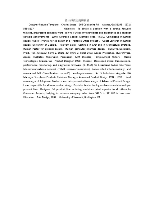
设计师英文简历模板Designer Resume Template Charles Lucas 266 Coldspring Rd. Atlanta, GA 31196 (271) 555-8217 __________________ Objective To obtain a position with a strong, forward thinking, progressive company were I can fully utilize my knowledge and experience as a designer. Notable Achievements 1997: Awarded Special Mention Prize. "ICSID/ Compiegne Industrial Design Award", France, for co-design of a "Portable Office Project". Guest Lecturer, Industrial Design, University of Georgia. Relevant Skills Certified in CAD and in Architectural Drafting. Human Factor for product design. Human computer interface design. CDRS(Pro/Designer), Pro/E, TDI, AutoCAD, Form Z, Strata 3D, Infini-D, Corel Draw, Adobe Photoshop, QuarkXPress, Adobe Illustrator, HyperCard, Persuasion, MM Director. Employment History Harris Technologies, Atlanta, GA Product Designer, 1998 - Present Developed critical transmissions, performance monitoring, and diagnostics firmware (C, ASM) for broadband hybrid fiber/coax telecommunications network (TDMA receiver/transmitter). Documented interface/design and maintained MR ("modification request") handling/response. A S Industries, Augusta, GA Manager, Telephone Products Division / Manager, Advanced Product Design, 1994 - 1998 Hired as manager of Telephone Products, and later promoted to manager of Advanced Product Design, I was responsible for all new product design. Provided key technology enhancements to multiple product lines. Designed full product line including machines rated superior to all others by Consumer Reports, helping to increase company sales from $42.3 to $71.8M in one year. Education B.A. Design, 1994 University of Vermont, Burlington, VT。
Resume

___________________________________________________________________________EducationA PR 04 – on going D EC 96 – A PR 02 Doctor of Philosophy Program, Faculty of Information Technology Monash University, AustraliaCurrent Project Title: Bezier curve enhancements and vertex-based genericshape coding.Bachelor of Science, Computer Science & Engineering (B. Sc. Engg.)Passed with 1st class grade in Apr 2002 Bangladesh University of Engineering and Technology (BUET), Dhaka.Thesis Title: Medical diagnostic system using neuro-fuzzy techniques.ExperienceA PR 04 –on going A PR 02 – A PR 04 Postgraduate ResearchMonash University, AustraliaCurrent Project Title:Bezier curve enhancements and vertex-based generic shapecodingDescription: There is often a large gap between the Bezier curve and its control polygon which makes it inefficient in shape coding applications. This project aims at reducing this gap so that it can be efficiently encode and represent the object shape and thus enhance the parametric curve based coding frameworks.Lecturer, Department of Computer Science and EngineeringInternational Islamic University Chittagong, Dhaka Campus, BangladeshResponsibilities:Teaching: Teaching B.Sc. courses of Computer Science of Engineering with full unit responsibilities.Project supervision: Supervise the undergraduate course projects.Research: Supervise the undergraduate project and thesis.Additional ExperienceJ UL04–J UN06 A PR 04 –on going Professional Software Development: Database project development for small business industries under Monash Regional Centre for ICT (MRCICT), Monash University, Gippsland. Subject Management: Advanced Multimedia and Network Technology (50%) @ Gippsland School of Information Technology, Monash University.Responsibilities:Lectures and tutorials for 6 weeks, preparing assignments, final exam questions, attending the newsgroup, marking the assignments and exam scripts, and managing the unit webpage.Casual Tutoring: Advanced Multimedia and Network Technology@ Gippsland School of Information Technology, Monash University.Responsibilities:Conduct tutorials for 12 weeks in Semester 2 of both 2004 and 2005.Causal Marking: Advanced Multimedia and Network Technology &Computer Graphics@ Gippsland School of Information Technology, Monash University.Responsibilities:Marking the Assignments in 2004, 2005 and 2006.Ferdous Ahmed SohelE-mail : Ferdous.Sohel@.auFerdous.Sohel@Phone : + 61-3-990-26133 (office)+ 61-3-512-23932 (home)+ 61-431 182 154 (mobile)Fax : + 61-3-990-26842 (office)ResumeProfessional SkillsReview WorksHardwareDevelopedSoftwareDevelopedInformation System DesignOthers Journal:Computer Aided Design, Elsevier Science, 2006.Conferences:International Conference on Computer and Information Technology, 2005.International Computer Software and Applications Conference, 2005.Projects:Computer Aided Automatic Security System, 4-bit Computer Design, ALU Design. Projects:Image Interactive Software, Student Admission and Information Management Systems, Games like Paranoid (in C/C++) and Batman (in PASCAL), File Transfer System among Computers on Network (in Java), File Management on-Disk like DOS (in 80X86 Assembler), Bangla Spread Sheet like MS-Excel (Visual Basic), Compiler Design (inC/C++)Projects: Analyse the Systems of PetroBangla, the Authority that deals and controls the exploration, transmission and distribution of Petroleum in Bangladesh.Programming Languages and Logics: Turbo Pascal, Turbo C/C++, Visual C/C++, Unix C, Java, HTML, 80x86 Assembly, Visual Basic, PrologTools And Libraries: MFC, MATLABDatabase Management Language: Oracle, SQLNatural Languages: English, Bangla___________________________________________________________________________Selected PublicationsBookChapterJournalArticlesConferenceArticlesB. Sc. Engg.Thesis (A complete list of publications is attached)• F.A. Sohel, G.C. Karmakar, and L.S. Dooley, "Video Coding for Mobile Communications," in Mobile Multimedia Communications: Concepts,Applications and Challenges, Idea Group Publishers, 2006• F.A. Sohel, L.S. Dooley, and G.C. Karmakar,“New dynamic enhancements to the vertex-based rate-distortion optimal shape coding framework,” IEEE Transactions on Circuits and Systems for Video Technology, revision submitted. • F.A. Sohel, G.C. Karmakar, and L.S. Dooley, “Fast distortion measurement using chord-length parameterisation within the vertex-based rate-distortionoptimal shape coding framework,” IEEE Signal Processing Letters, accepted. • F.A. Sohel, L.S. Dooley, and G.C. Karmakar, “Accurate distortion measurement for generic shape coding,” Pattern Recognition Letters, vol.27, no.2, pp.133-142, 2006.• F.A. Sohel, L.S. Dooley, and G.C. Karmakar,“Variable width admissible control point band for vertex based operational-rate-distortion optimal shape coding algorithms,” IEEE International Conference on Image Processing, ICIP-06, in press.• F.A. Sohel, G.C. Karmakar, L.S. Dooley, and J. Arkinstall, “Enhanced Bezier curve models incorporating local information,” IEEE International Conference on Acoustics, Speech, and Signal Processing, ICASSP-05, vol. IV, pp. 253-256, ISBN: 0-7803-8875-5, March, 2005, Philadelphia, PA, USA.• F.A. Sohel, L.S. Dooley, and G.C. Karmakar, “A dynamic Bezier curve model,”IEEE International Conference on Image Processing, ICIP-05, vol. II, pp. 474-477, ISBN: 0-7803-9135-7, September, 2005, Genoa, Italy.• F.A. Sohel, “Medical diagnostic system using neuro-fuzzy techniques,”Bangladesh University of Engineering and Technology, Bangladesh, Apr. 2002.Awards/ AchievementsA PR04– O CT07 D EC04– A PR02 D EC04– A PR02 J UL93– J UN95 J AN88-J UN93 Monash Departmental Scholarships for PhDDean’s Scholarship for Brilliant Result in the Junior level in undergrad Examinations, by Bangladesh University of Engineering and Technology,BangladeshMerit Scholarship for Brilliant Result in the HSC (12 class equivalent) Exam in the Board of Intermediate Secondary and Education, Dhaka, Bangladesh.Merit Scholarship for Brilliant Result in the SSC (10 class equivalent) Exam in the Board of Intermediate Secondary and Education, Dhaka, Bangladesh.Merit Scholarship for obtaining both Junior and Primary Scholarships Provided by the Government of Bangladesh.___________________________________________________________________________ ActivitiesJ AN 04 – D EC 06 J AN 06 – D EC 06 J AN 06 – D EC 06 J AN 06 – D EC 06 J AN 05 – D EC 05 Student Member, IEEE.President, Gippsland Association of Postgraduate Students, Monash University. Representative, Monash University Postgraduate Association.Member, Monash University Gippsland Students Union (MUGSU) board. Treasurer, Gippsland Association of Postgraduate Students, Monash University.___________________________________________________________________________ReferencesProfessor Laurence Sean DooleyChair of Multimedia Technology and Director of Monash Regional Centre forICT, Monash UniversityGippsland School of Information TechnologyMonash University, Gippsland Campus, Vic – 3842.Tel: + 61-3-990-26628.Fax: + 61-3-990-26842.Email: Laurence.Dooley@.auDr. Gour Chandra KarmakarLecturerGippsland School of Information TechnologyMonash University, Gippsland Campus, Vic – 3842.Tel: + 61-3-990-26252.Fax: + 61-3-990-26842.Email: Gour.Karmakar@.auProfessor Chowdhury Mofizur RahmanPro-Vice ChancellorUnited International University, Dhaka, BangladeshTel: + 880-2-9125912-5.Fax: + 880-2- 9125916.Email: cmr@uiu.ac.bdResearchInterests Signal/Image ProcessingParametric curvesShape coding PersonalParticularsFull Name Father’s Name Mother’s NamePassport Date of Birth Place of BirthHobbies Postal Address Ferdous Ahmed SohelMohammed FaruqueAyesha SiddiquiBangladeshi11 September 1977Munshiganj, BangladeshPlaying Cricket, Soccer20 McDonald Way, Churchill, Vic 3842, AustraliaDate:30July2006Publication ListsRefereed Journal Papers:1. F.A. Sohel, L.S. Dooley, and G.C. Karmakar,“New dynamic enhancements to the vertex-basedrate-distortion optimal shape coding framework,” IEEE Transactions on Circuits and Systems for Video Technology, revision submitted.2. F.A. Sohel, G.C. Karmakar, and L.S. Dooley, “Fast distortion measurement using chord-lengthparameterisation within the vertex-based rate-distortion optimal shape coding framework,”IEEE Signal Processing Letters, in press.3. F.A. Sohel, L.S. Dooley, and G.C. Karmakar, “Accurate distortion measurement for genericshape coding,” Pattern Recognition Letters, vol.27, no.2, pp.133-142, 2006.4. F.A. Sohel and C.M. Rahman, “Association rule mining in dynamic database using the conceptof border sets,” Asian Journal of Information Technology, vol.3, no.7, pp. 508-515, 2004.Lecture Notes Series:1. F.A. Sohel, G.C. Karmakar, and L.S. Dooley, "An improved shape descriptor using Beziercurves," Lecture Notes in Computer Science, Springer Verlag, vol. 3776, pp.401-406, 2005.Refereed conference papers:1. F.A. Sohel, L.S. Dooley, and G.C. Karmakar,“Variable width admissible control point band forvertex based operational-rate-distortion optimal shape coding algorithms,” IEEE International Conf. Image Proc., ICIP-06, in press.2. F.A. Sohel, G.C. Karmakar, and L.S. Dooley, “Dynamic sliding window width selectionstrategies for rate-distortion optimal vertex-based shape coding algorithms,” International Conference on Signal Processing, ICSP-06, in press.3. F.A. Sohel, G.C. Karmakar, and L.S. Dooley, "An improved shape descriptor using Beziercurves," First International Conference on Pattern Recognition and Machine Intelligence, PReMI-05, December, 2005, Kolkata, India.4. F.A. Sohel, L.S. Dooley, and G.C. Karmakar, “A novel half-way shifting Bezier curve model,”IEEE Region 10 Conference, Tencon-05, November, 2005, Melbourne, Australia.5. F.A. Sohel, L.S. Dooley, and G.C. Karmakar, “A dynamic Bezier curve model,” IEEEInternational Conference on Image Processing, ICIP-05, vol. II, pp. 474-477, ISBN: 0-7803-9135-7, September, 2005, Genoa, Italy.6. F.A. Sohel, G.C. Karmakar, L.S. Dooley, and J. Arkinstall, “Enhanced Bezier curve modelsincorporating local information,” IEEE International Conference on Acoustics, Speech, and Signal Processing, ICASSP-05, vol. IV, pp. 253-256, ISBN: 0-7803-8875-5, March, 2005, Philadelphia, PA, USA.7. F.A. Sohel, G.C. Karmakar, and L.S. Dooley, “A generic shape descriptor using Bezier curves,”International Conference on Information Technology, ITCC-05, vol. II. pp. 95-100, April, 2005, Las Vegas, Nevada, USA.8. F.A. Sohel, L.S. Dooley, and G.C. Karmakar, “A modified distortion measurement algorithmfor shape coding,” Proceedings of the 3rd Workshop on the Internet, Telecommunication and Signal Processing, WITSP-04, December, 2004, Adelaide, Australia.9. F.A. Sohel, “A new neural network with fuzzy technique: disease diagnosis, a case study,”Proceedings of International Conference on Computers and Information technology, ICCIT-03, pp. 713 – 716, December 2003, Dhaka, Bangladesh.10.F.A. Sohel and C.M. Rahman, “Association Rule Mining in Dynamic Database using theConcept of Border Sets” – in Proceedings of 3rd International Conference on Electrical, Electronics and Computer Engineering, ICEECE-03, pp. 165-170, December 2003, Dhaka, Bangladesh.11.F.A. Sohel and M. Amiruzzaman, “Fingerprint authentication system using back-propagation,”Proceedings of International Conference on Computers and Information technology, ICCIT-03, pp. 722-725, December 2003, Dhaka, Bangladesh.12.F.A. Sohel, C.M. Rahman, and G.C. Karmakar, “Automatic video object segmentationframework from VOP,” Proceedings of 3rd International Conference on Electrical, Electronics and Computer Engineering, ICEECE-03, pp. 192-196, December 2003, Dhaka, Bangladesh. 13.C.M. Rahman, F.A. Sohel, P. Naushad, and S.M. Kamruzzaman, “Text classification using theconcepts of data mining association rules,” Proceedings of International Conference on Information Technology: Prospects and Challenges in the 21st century, ITPC-03, pp. 234-241, May 2003, Kathmandu, Nepal.Non-refereed Publications:1. F.A. Sohel, L.S. Dooley, and G.C. Karmakar, “Modified model for Bezier curves,” GSCITtechnical report series, TR- 2004/13, September, 2004.2. F.A. Sohel, G.C. Karmakar, and L.S. Dooley, “A novel half-way shifting Bezier curve modelwith improved error bound,” GSCIT technical report series, TR- 2004/14, October, 2004.3. F.A. Sohel, G.C. Karmakar, and L.S. Dooley, “Adaptive Sliding Window Width SelectionStrategies for Vertex-Based Shape Coding,” GSIT technical report series, TR-2005/5, October, 2005.4. F.A. Sohel, L.S. Dooley, and G.C. Karmakar, “Mini-Max Bound of the Width of AdmissibleControl Point Band for Vertex-Based ORD Optimal Shape Coding Algorithms,” GSIT technical report series, TR-2005/6, October, 2005.5. F.A. Sohel, G.C. Karmakar, and L.S. Dooley, “A fast distortion measurement using chord-length parameterisation within the vertex-based operational rate-distortion optimal shape coding framework,” GSIT technical report series, TR-2006/2, March, 2006.。
高中新教材英语课件选择性必修第四册LaunchingYourCareerSectionⅠReadin

Analysis of key vocabulary, phrases, and sentence structures
1
Key vocabulary
2
Phrases
3
Sentence patterns
career planning, self-awareness, job exploration, professional qualities, skills development, etc.
03
Imparting knowledge and skills in career planning
Discussion on the Basic Principles and Methods of Career Planning
1 Understanding oneself
Through self-assessment, understanding one's interests, values, skills, and strengths provides a foundation for career planning.
Teaching methods
Utilize modern teaching methods such as multimedia courseware and online resources to create vivid teaching scenarios and stimulate students' interest and enthusiasm in learning. At the same time, encourage students to use their extracurricular time to expand their reading and practical activities, and improve their English application ability.
英语六级常用的易错易混词

21、22
01
assembl e
02
resembl e
03
assign
04
design
06
聚积,集 合;装配
07
与……想 象
08
分配,指 责
09
车机,谋 划,构思
05resign10来自辞职23、24
assist consist exist insist persist resist
援助,帮助 由……组成,在于 存在,生存 坚持,强调 坚持,持续 抵抗,反抗
内容,容量,目录 范围,程度 意图,目的 有力的,有效的
contemporary 当代的,同时代的
temporary
暂时的,临时的
continual continuous
连续的,频繁的(中间有稍歇的) 连续的,持续地(中间无停顿的)
66、67、68
consent consult result conservation 愤恨,怨恨 侮辱,凌辱 会话,谈话
49、50、51
composition proposition comprehensive concept 博览会,展览会,说明,暴露 可理解的,易领会的 自负,自夸
exposition comprehensible conceit 写作,作文,成份 主张,建议 全面的,综合的 观念,概念
52、53
colorful comical commend 有色的,有色人种的 戏剧的,有趣的,滑稽演员 命令 推荐,介绍
42、43
coincide collect recollect 决定,约束 选举,推选
decide elect select 自杀,自毁 忽视,疏忽
Resume

Main Comments(推荐评价):1. About 7 years experience in designing field.2. Good at the evening dress designing.3. Proficient to use design software (Photoshop, Illustrator, AutoCAD, CorelDraw).4. Fluent English in writing and speaking.RESUMEPersonal ParticularsPost Applied Dress DesignerName TANG YingDate of Birth 1980/02Gender FemaleMarital Status SingleTelephone NumberEducational Background[Highest level]Degree Bachelor DegreeMajor Fashion DesigningGraduation Date 2008/01Name of institution Donghua University[The second Highest level]Degree College DegreeMajor Fashion DesigningGraduation Date 2002/07Name of institution Jiangnan UniversityEnglish FluentEmployment History1. Company name Voed ApparelTitle Fashion/Textiles DesignerResponsibility 1. In charge of the beginning of new season preparing trendresearch and trend analysis from fabric, color, styles,accessories, technical detail design and graphics.2. Responsible for designing fashion style,graphic and printdrawing.3. Responsible for the tech park design for AKA girl and MEC girl2011 after styles list finished.Reason of Demission Shanghai office will be re-located to XiamenDate Joined 2010/05 Date Left : Present2. Company name An Ru Ting Fashion CompanyInterview by a client of a candidate supplied by Uniland shall beTitle DesignerResponsibility 1. Major in dress design and good at the evening dress, skirt designand some special details design.2. Prepare the inspiration from the “Show Details” magazines andDie Xun fashion information.3. Make collection from color to styles, details.4. Select and buy the fabric and accessories from the suppliers andmarket.5. Draw the sketches by hand, buy samples, discuss pattern withpattern department before sample finish.Date Joined 2008/09 Date Left : 2010/043. Company name NTS Fashion CompanyTitle Graphic Artist/DesignerResponsibility 1. Research fashion and consumer trends before creating a newline.2. Go to fabric market to select fabric and color and refabricate thenew color and pattern for our collection.3. Go to accessories market to choose the belts, buttons, and othertrimmings.4. Create styles for the line from German retailers and chinawholesaler market.Date Joined 2005/08 Date Left : 2008/084. Company name CVC Fashion CompanyTitle Fashion DesignerResponsibility 1. Collect brand popular trend.2. Select fabrics.3. Draw style diagram.Date Joined 2004/05 Date Left : 2005/025. Company name Kolon International Corp. Nanjing OfficeTitle MerchandiserResponsibility 1. Help to finish the pre-production sample.2. Go to factory to check the fabric & accessory.3. Check the order's cutting, sewing, packing.Date Joined 2003/02 Date Left : 2004/05Interview by a client of a candidate supplied by Uniland shall be。
2023年实用文_英文求职自荐信范文九篇

2023年英文求职自荐信范文九篇英文求职自荐信篇1Dear leaders:How are you!Thank you for your busy schedule to review my written submissions,thank you! My name is __, Shaanxi Radio and Television University Chinese Language and Literature 04, a graduating student。
After several years of the Qian Xiu, the long hard training, I was finally about to a qualified university graduates of the identity of the times of the Zhenqian accept forward to your selection and always be ready to own the school dedicated to you are my common cause。
I will not claim that he is a talent, but I believe that my fighting spirit and enterprising spirit。
Three years of study at the university journey, I have studied earnestly and assiduously to achieve good results。
Through the school's culture and their own efforts, I not only possess the required expertise in Chinese listening, speaking, reading,writing and other basic capabilities, but also possess the required basic professional teacher quality, and knowing how to use psychology,pedagogy, the basic principles of to carry out the class teacher teaching activities; to master the professional knowledge, I also made full use of spare time to learn the computer programs, and also obtained the corresponding NIT—based computer application modules (word, excel,powerpoint) certificate。
ua设计师应聘的流程

ua设计师应聘的流程英文回答:The process of applying for a UI designer position can vary depending on the company and industry. However, there are some common steps that most applicants will go through.Firstly, it is important to prepare a strong resume and portfolio showcasing your relevant skills and experience. This is the first impression that potential employers will have of you, so it is crucial to make it stand out. Your resume should highlight your design experience, software proficiency, and any notable projects you have worked on. Your portfolio should include examples of your design work, demonstrating your ability to create visually appealing and user-friendly interfaces.Once your application materials are ready, the next step is to start applying for positions. This can be done through various channels such as online job boards, companywebsites, or networking events. It is important to tailor your application to each specific job posting, highlighting the skills and experiences that are most relevant to the position.After submitting your application, you may be invited for an interview. This can be conducted in person, over the phone, or through video conferencing. The interview is an opportunity for the employer to assess your technical skills, problem-solving abilities, and cultural fit within the company. They may ask you to complete a design exercise or provide examples of your previous work.If you pass the interview stage, the next step is typically a second interview or a design challenge. This is an opportunity for you to showcase your design process and problem-solving abilities. You may be given a specific design problem to solve or asked to critique an existing interface. This stage is crucial in demonstrating your ability to think critically and creatively.Finally, if you are successful in the previous stages,you may be offered the position. At this point, it is important to negotiate your salary and benefits package. This can include discussing your desired salary, vacation time, and any other perks that are important to you. Once the terms are agreed upon, you can formally accept the offer and begin the onboarding process.中文回答:申请UI设计师职位的流程可能因公司和行业而异。
