AS3901中文资料
ZSPM9000Al1R中文资料(ZMDI)中文数据手册「EasyDatasheet - 矽搜」

桥梁字段名称
/****** Script for SelectTopNRows command from SSMS ******/ SELECT K0112as路线简称C,A0102as管理单位,HA0102as管理单位名称,A1316as改造完工日期C,A1317as改造部位D,HA1317as改造部位中文,A1319,as是否部补助项目DHA1319as是否部补助项目中文,A1307as已采取交通管制措施D,HA1307as已采取交通管制措施中文,K6029as总造价N,K0144as工程号C,K6031as施工单位名称C,K6030as设计单位名称C,K6032as监理单位名称C,K6079as建设单位名称C,K0116as通车日期C,K0199as备注M,A9902as原管理单位D,HA9902as原管理单位中文,A9903as原路线代码C,K6100as修建年度C,A9904as操作顺序D,HA9904as操作顺序中文,A9905as平移值N,A9906as是否桩号反向重排D,HA9906as是否桩号反向重排中文,A9908,as反排路线里程NA9907,as是否删除D HA9907,K6111,as上部结构材料D HK6111,K6112,as监管单位名称CV0116,as变更原因说明CKBSBM,as标识编码CK3902,as竣工日期CK3901,as开工日期CKI6002,as分离式类别D HKI6002,KI6003,as是否高架桥D HKI6003,KI6004,as建筑面积(平米)NKI6005,as是否匝道立交桥D HKI6005,KI6006,as是否重复立交桥D HKI6006,K3905,as改建变更原因D HK3905,K0191,as改建变更日期(最近一次作为改建数纳入统计的时间)CA0131,as管养单位性质D HA0131,K3904,as路网调整类型D HK3904,V0310,as计划项目唯一编码CV0311,as计划项目路线编码CV0312,as计划项目路线名称CA1318,as工程性质D HA1318,V0315,as计划项目桥梁桩号NK0101,as路线代码CK6003,as桥梁中心桩号NA0103,as行政区划D HA0103,K6001,as桥梁编号CK6002,as桥梁名称CK6070,as桥梁所在地点CA1302,as收费性质D HA1302,A1314,as管养单位名称CK2010,as管养单位所属行业类别D HK2010, K6006,as跨越地物名称CK6005,as跨越地物类型D HK6005,K6080,as桥梁用途分类D HK6080,K6004,as按使用年限分D HK6004,K6007,as桥梁跨径分类D HK6007,K6028,as技术状况评定D HK6028,A1305,as评定日期CA1315,as最近定期检查日期CK6089,as是否公铁立交D HK6089,K6062,as立交桥类别D HK6062,K6077,as立交桥跨越各路线CK6078,as立交桥连通各路线CK6008,as桥梁全长(米)NK0185,as经度NK0186,as纬度NK6065,as跨径总长(米)NK6063,as单孔最大跨径(米)NK6064,as桥梁跨径组合(孔*米)CK6071,as桥梁孔数(孔)NK6010,as主桥孔数(孔)NK6011,as主桥主跨(米)NK6012,as主桥边跨(米)NK6013,as前引桥长(米)NK6014,as后引桥长(米)NK6066,as桥梁全宽(米)NK6009,as桥面净宽(米)NK6069,as人行道宽(米)NK1210,as行车道宽(米)NK6081,as桥梁高度(米)NK6082,as桥面标高(米)NK6015,as桥下净空(米)NA0521,as匝道(平米)NA0531,as匝道(公里)NK6016,as上部结构类型D HK6016,K6068,as下部结构形式D HK6068,K6083,as基础结构型式D HK6083,K6084,as引桥结构型式D HK6084,K6021,as支座类型D HK6021,K6018,as桥台类型D HK6018,K6017,as桥墩类型D HK6017,A1328,as墩台防撞设施类型D HA1328, K6020,as伸缩缝类型D HK6020,K6085,as拱桥矢跨比CK6086,as桥面纵坡NK6087,as桥面线型D HK6087,K6025,as弯坡斜特征D HK6025,K6088,as桥位地形D HK6088,K6019,as桥面铺装类型D HK6019,A1306,as主要病害位置D HA1306,K6072,as主要病害描述CK6090,as下部材料类型CK6091,as主桥截面型式D HK6091,K6092,as引桥截面型式D HK6092,K6022,as设计荷载等级D HK6022,K6033,as桥梁验算荷载D HK6033,K6023,as抗震等级D HK6023,K6093,as河床地质及纵坡D HK6093, K6094,as河床最低标高(米)NK6060,as设计洪水频率(年)NK6095,as设计洪水位NK6096,as常年水位NK6024,as通航等级D HK6024,K6099,as寻常洪水位NK6097,as历史最高洪水位NK6098,as河床变迁CFROM[k60_shanghai].[dbo].[K060]。
AS431I中文资料
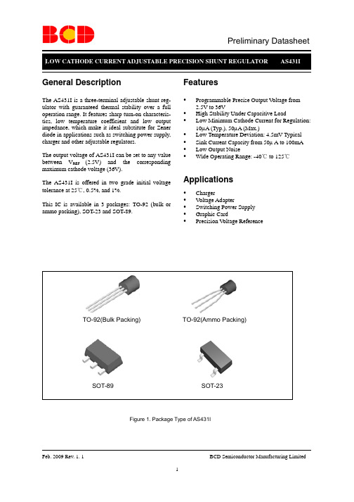
CATHODE
REF
+
-
VREF
Feb. 2009 Rev. 1. 1
ANODE Figure 3. Functional Block Diagram of AS431I
BCD Semiconductor Manufacturing Limited 2
770
SOT-23
370
150
-65 to 150
2000
Unit
V mA mA
mW
°C °C V
Note 1: Stresses greater than those listed under “Absolute Maximum Ratings” may cause permanent damage to the device. These are stress ratings only, and functional operation of the device at these or any other conditions beyond those indicated under “Recommended Operating Conditions” is not implied. Exposure to “Absolute Maximum Ratings” for extended periods may affect device reliability.
2.525 8 10 16
-1.0 -2.7
-0.5 -2.0
3.6 10
2
4
10
50
0.05 1.0 0.15 0.5
68 70 113
Unit
MAX3901-MAX3902中文资料

PARAMETER
SYMBOL
CONDITION
POWER SUPPLY
Operating Power-Supply Current
ICC
TJ < +100°C TJ < +140°C
Standby Current Power-Up Time
ISTBY tPU
TJ < +85°C TJ < +125°C From valid VCC to STATUS low
Subassembly
Ordering Information
PART
TEMP RANGE
PIN-PACKAGE
MAX3901E/D
-40°C to +140°C
Dice*
MAX3902E/D
-40°C to +140°C
Dice*
*Dice are designed to operate over a -40°C to +140°C junction temperature (Tj) range, but are tested and guaranteed at TA = +75°C.
Both circuits provide an input power detect and lowpower standby mode with status output. No filter capacitors are required in the optical subassembly, thus enabling a low-cost receiver design. The circuits are available in die and wafer form.
纳米颗粒尺寸、形状以及界面效应对介电和击穿场强等因素的影响

Society Chem.Mater.2010,22,1567–15781567DOI:10.1021/cm902852hNanoparticle,Size,Shape,and Interfacial Effects on Leakage Current Density,Permittivity,and Breakdown Strength of MetalOxide-Polyolefin Nanocomposites:Experiment and TheoryNeng Guo,†Sara A.DiBenedetto,†Pratyush Tewari,‡Michael nagan,*,‡Mark A.Ratner,*,†and Tobin J.Marks*,††Department of Chemistry and the Materials Research Center,Northwestern University,Evanston, Illinois60208-3113and‡Center for Dielectric Studies,Materials Research Institute,The Pennsylvania State University,University Park,Pennsylvania16802-4800Received September11,2009.Revised Manuscript Received December2,2009A series of0-3metal oxide-polyolefin nanocomposites are synthesized via in situ olefin polymeriza-tion,using the following single-site metallocene catalysts:C2-symmetric dichloro[rac-ethylenebisindenyl]-zirconium(IV),Me2Si(t BuN)(η5-C5Me4)TiCl2,and(η5-C5Me5)TiCl3immobilized on methylaluminoxane (MAO)-treated BaTiO3,ZrO2,3-mol%-yttria-stabilized zirconia,8-mol%-yttria-stabilized zirconia, sphere-shaped TiO2nanoparticles,and rod-shaped TiO2nanoparticles.The resulting composite materials are structurally characterized via X-ray diffraction(XRD),scanning electron microscopy(SEM), transmission electron microscopy(TEM),13C nuclear magnetic resonance(NMR)spectroscopy,and differential scanning calorimetry(DSC).TEM analysis shows that the nanoparticles are well-dispersed in the polymer matrix,with each individual nanoparticle surrounded by polymer.Electrical measurements reveal that most of these nanocomposites have leakage current densities of∼10-6-10-8A/cm2;relative permittivities increase as the nanoparticle volume fraction increases,with measured values as high as6.1. At the same volume fraction,rod-shaped TiO2nanoparticle-isotactic polypropylene nanocomposites exhibit significantly greater permittivities than the corresponding sphere-shaped TiO2nanoparticle-isotactic polypropylene nanocomposites.Effective medium theories fail to give a quantitative description of the capacitance behavior,but do aid substantially in interpreting the trends qualitatively.The energy storage densities of these nanocomposites are estimated to be as high as9.4J/cm3.IntroductionFuture pulsed-power and power electronic capacitors will require dielectric materials with ultimate energy storage den-sities of>30J/cm3,operating voltages of>10kV,and milli-second-microsecond charge/discharge times with reliable operation near the dielectric breakdown limit.Importantly, at2and0.2J/cm3,respectively,the operating characteristics of current-generation pulsed power and power electronic capacitors,which utilize either ceramic or polymer dielectric materials,remain significantly short of this goal.1An order-of-magnitude improvement in energy density will require the development of dramatically different types of materials, which substantially increase intrinsic dielectric energy den-sities while reliably operating as close as possible to the die-lectric breakdown limit.For simple linear response dielectric materials,the maximum energy density is defined in eq1,U e¼12εrε0E2ð1Þwhereεr is the relative dielectric permittivity,E the dielec-tric breakdown strength,andε0the vacuum permittivity (8.8542Â10-12F/m).Generally,metal oxides have large permittivities;however,they are limited by low breakdown fields.While organic materials(e.g.,polymers)can provide high breakdown strengths,their generally modest permit-tivities have limited their application.1Recently,inorganic-polymer nanocomposite materials have attracted great interest,because of their potential for high energy densities.2By integrating the complementary*Authors to whom correspondence should be addressed.E-mail addresses: mxl46@(M.T.L.),ratner@(M.A.R.),and t-marks@(T.J.M.).(1)(a)Pan,J.;Li,K.;Li,J.;Hsu,T.;Wang,Q.Appl.Phys.Lett.2009,95,022902.(b)Claude,J.;Lu,Y.;Li,K.;Wang,Q.Chem.Mater.2008, 20,2078–2080.(c)Chu,B.;Zhou,X.;Ren,K.;Neese,B.;Lin,M.;Wang,Q.;Bauer,F.;Zhang,Q.M.Science2006,313,334–336.(d) Cao,Y.;Irwin,P.C.;Younsi,K.IEEE Trans.Dielectr.Electr.Insul.2004,11,797–807.(e)Nalwa,H.S.,Ed.Handbook of Low and High Dielectric Constant Materials and Their Applications;Academic Press:New York,1999;V ol.2.(f)Sarjeant,W.J.;Zirnheld,J.;MacDougall,F.W.IEEE Trans.Plasma Sci.1998,26,1368–1392.(2)(a)Kim,P.;Doss,N.M.;Tillotson,J.P.;Hotchkiss,P.J.;Pan,M.-J.;Marder,S.R.;Li,J.;Calame,J.P.;Perry,J.W.ACS Nano 2009,3,2581–2592.(b)Li,J.;Seok,S.I.;Chu,B.;Dogan,F.;Zhang, Q.;Wang,Q.Adv.Mater.2009,21,217–221.(c)Li,J.;Claude,J.;Norena-Franco,L.E.;Selk,S.;Wang,Q.Chem.Mater.2008,20, 6304–6306.(d)Gross,S.;Camozzo,D.;Di Noto,V.;Armelao,L.;Tondello,E.Eur.Polym.J.2007,43,673–696.(e)Gilbert,L.J.;Schuman,T.P.;Dogan,F.Ceram.Trans.2006,179,17–26.(f)Rao,Y.;Wong,C.P.J.Appl.Polym.Sci.2004,92,2228–2231.(g)Dias,C.J.;Das-Gupta,D.K.IEEE Trans.Dielectr.Electr.Insul.1996,3,706–734.(h)Mammone,R.R.;Binder,M.Novel Methods For Preparing Thin,High Permittivity Polymerdielectrics for Capacitor Applica-tions;Proceedings of the34th International Power Sources Symposium, 1990,Cherry Hill,NJ;IEEE:New York,1990;pp395-398./cmPublished on Web01/05/2010 r2010American Chemical1568Chem.Mater.,Vol.22,No.4,2010Guo et al.properties of their constituents,such materials can simul-taneously derive high permittivity from the inorganic in-clusions and high breakdown strength,mechanical flexibility,facile processability,light weight,and tunability of the properties(polymer molecular weight,comonomer incorporation,viscoelastic properties,etc.)from the poly-mer host matrix.3In addition,convincing theoretical argu-ments have been made suggesting that large inclusion-matrix interfacial areas should afford greater polarization levels,dielectric response,and breakdown strength.4 Inorganic-polymer nanocomposites are typically pre-pared via mechanical blending,5solution mixing,6in situ radical polymerization,7and in situ nanoparticle syn-thesis.8However,host-guest incompatibilities intro-duced in these synthetic approaches frequently result in nanoparticle aggregation and phase separation over largelength scales,9which is detrimental to the electrical prop-erties of the composite.10Covalent grafting of the poly-mer chains to inorganic nanoparticle surfaces has alsoproven promising,leading to more effective dispersionand enhanced electrical/mechanical properties;11how-ever,such processes may not be optimally cost-effective,nor may they be easily scaled up.Furthermore,thedevelopment of accurate theoretical models for the di-electric properties of the nanocomposite must be accom-panied by a reliable experimental means to achievenanoparticle deagglomeration.In the huge industrial-scale heterogeneous or slurryolefin polymerization processes practiced today,SiO2isgenerally used as the catalyst support.12Very large localhydrostatic pressures arising from the propagating poly-olefin chains are known to effect extensive SiO2particlefracture and lead to SiO2-polyolefin composites.12Based on this observation,composite materials with enhancedmechanical properties13have been synthesized via in situpolymerizations using filler surface-anchored Ziegler-Natta or metallocene polymerization catalysts.14There-fore,we envisioned that processes meditated by rationallyselected single-site metallocene catalysts supported onferroelectric oxide nanoparticles15might disrupt ubiqui-tous and problematic nanoparticle agglomeration,16toafford homogeneously dispersed nanoparticles within thematrix of a processable,high-strength commodity poly-mer,already used extensively in energy storage capaci-tors.17Moreover,we envisioned that the methylalumino-xane(MAO)co-catalyst14i layer applied to the metaloxide nanoparticle surfaces would,after polymer workupunder ambient conditions,serve as an effective precursorfor a thin Al2O3layer to moderate the large anticipated(3)(a)Nelson,J.K.;Hu,Y.J.Phys.D:Appl.Phys.2005,38,213–222.(b)Tanaka,T.;Montanari,G.C.;M€u lhaupt,R.IEEE Trans.Dielectr.Electr.Insul.2004,11,763–784.(c)Lewis,T.J.IEEE Trans.Dielectr.Electr.Insul.1994,15,812–825.(d)Newnham,R.E.Annu.Rev.Mater.Sci.1986,16,47–68.(4)(a)Saha,S.K.Phys.Rev.B2004,69,1254161–125464.(b)Nelson,J.K.;Utracki,L.A.;MacCrone,R.K.;Reed,C.W.IEEE Conf.Electr.Insul.Dielectr.Phenomena2004,314–317.(c)Li,J.Phys.Rev.Lett.2003,90,217601/1–4.(5)(a)Subodh,G.;Deepu,V.;Mohanan,P.;Sebastian,M.T.Appl.Phys.Lett.2009,95,062903.(b)Dang,Z.;Wu,J.;Fan,L.;Nan,C.Chem.Phys.Lett.2003,376,389–394.(6)(a)Goyal,R.K.;Jagadale,P.A.;Mulik,U.P.J.Appl.Polym.Sci.2009,111,2071–2077.(b)Afzal,A.B.;Akhtar,M.J.;Nadeem,M.;Hassan,M.M.J.Phys.Chem.C2009,113,17560–17565.(c)Huang, X.Y.;Jiang,P.K.;Kim,C.U.J.Appl.Phys.2007,102,124103.(d) Parvatikar,N.;Ambika Prasad,M.V.N.J.Appl.Polym.Sci.2006, 100,1403–1405.(e)Badheka,P.;Magadala,V.;Gopi Devaraju,N.;Lee,B.I.;Kim,E.S.J.Appl.Polym.Sci.2006,99,2815–2821.(f)Xie, S.;Zhu,B.;Xu,Z.;Xu,Y.Mater.Lett.2005,59,2403–2407.(g) Schroeder,R.;Majewski,L.;Grell,M.Adv.Mater.2005,17,1535–1539.(h)Bai,Y.;Cheng,Z.;Bharti,V.;Xu,H.;Zhang,Q.Appl.Phys.Lett.2000,76,3804–3806.(7)(a)Andou,Y.;Jeong,J.-M.;Nishida,H.;Endo,T.Macromolecules2009,42,7930–7935.(b)Thomas,P.;Dwarakanath,K.;Varma,K.B.R.Synth.Met.2009,159,2128–2134.(c)Chen,Y.-M.;Lin,H.-C.;Hsu,R.-S.;Hsieh,B.-Z.;Su,Y.-A.;Sheng,Y.-J.;Lin,J.-J.Chem.Mater.2009,21,4071–4079.(d)He,A.;Wang,L.;Li,J.;Dong,J.;Han,C.C.Polymer2006,47,1767–1771.(e)Ginzburg,V.V.;Myers, K.;Malowinski,S.;Cieslinski,R.;Elwell,M.;Bernius,M.Macro-molecules2006,39,3901–3906.(f)Mizutani,T.;Arai,K.;Miyamoto, M.;Kimura,Y.J.Appl.Polym.Sci.2006,99,659–669.(g)Xiao,M.;Sun,L.;Liu,J.;Li,Y.;Gong,K.Polymer2002,43,2245–2248.(h)R.Popielarz,R.;Chiang,C.K.;Nozaki,R.;Obrzut,J.Macromolecules 2001,34,5910–5915.(8)(a)Balan,L.;Jin,M.;Malval,J.-P.;Chaumeil,H.;Defoin,A.;Vidal,L.Macromolecules2008,41,9359–9365.(b)Lu,J.;Moon,K.S.;Xu,J.;Wong,C.P.J.Mater.Chem.2006,16,1543–1548.(c)Yogo, T.;Yamamoto,T.;Sakamoto,W.;Hirano,S.J.Mater.Res.2004,19, 3290–3297.(9)(a)Vaia,R.A.;Maguire,J.F.Chem.Mater.2007,19,2736–2751.(b)Mackay,M.E.;Tuteja,A.;Duxbury,P.M.;Hawker,C.J.;Van Horn,B.;Guan,Z.;Chen,G.;Krishnan,R.S.Science2006,311,1740–1743.(c)Lin,Y.;Boeker,A.;He,J.;Sill,K.;Xiang,H.;Abetz,C.;Li,X.;Wang,J.;Emrick,T.;Long,S.;Wang,Q.;Balazs,A.;Russell,T.P.Nature2005,434,55–59.(10)(a)Stoyanov,H.;Mc Carthy,D.;Kollosche,M.;Kofod,G.Appl.Phys.Lett.2009,94,232905.(b)Chen,G.;Davies,A.E.IEEE Trans.Dielectr.Electr.Insul.2000,7,401–407.(c)Khalil,M.S.IEEE Trans.Dielectr.Electr.Insul.2000,7,261–268.(11)(a)Zhang,Y.;Ye,Z.Macromolecules2008,41,6331–6338.(b)Maliakal,A.;Katz,H.E.;Cotts,P.M.;Subramoney,S.;Mirau,P.J.Am.Chem.Soc.2005,127,14655–14662.(c)Rusa,M.;Whitesell,J.K.;Fox,M.A.Macromolecules2004,37,2766–2774.(d)Bartholome,C.;Beyou,E.;Bourgeat-Lami,E.;Chaumont,P.;Zydowicz,N.Macro-molecules2003,36,7946–7952.(e)Corbierre,M.K.;Cameron,N.S.;Sutton,M.;Mochrie,S.G.J.;Lurio,L.B.;R€u hm,A.;Lennox,R.B.J.Am.Chem.Soc.2001,123,10411–10412.(f)von Werne,T.;Patten,T.E.J.Am.Chem.Soc.2001,123,7497–7505.(g)Nuss,S.;B€o ttcher,H.;Wurm,H.;Hallensleben,M.L.Angew.Chem.,Int.Ed.2001,40, 4016–4018.(12)(a)Kaminsky,W.;Funck,A.;Wiemann,K.Macromol.Symp.2006,239,1–6.(b)Li,K.-T.;Kao,Y.-T.J.Appl.Polym.Sci.2006,101, 2573–2580.(c)du Fresne von Hohenesche,C.;Unger,K.K.;Eberle,T.J.Mol.Catal.A:Chem.2004,221,185–199.(d)Fink,G.;Steinmetz,B.;Zechlin,J.;Przybyla,C.;Tesche,B.Chem.Rev.2000,100,1377–1390.(13)(a)Dubois,P.;Alexandre,M.;J e r^o me,R.Macromol.Symp.2003,194,13–26.(b)Kaminsky,W.Macromol.Chem.Phys.1996,197, 3907–3945.(14)For recent reviews of single-site olefin polymerization,see:(a)Amin,S.B.;Marks,T.J.Angew.Chem.,Int.Ed.2008,47,2006–2025.(b)Marks,T.J.,ed.Proc.Natl.Acad.Sci.,U.S.A.,2006,103, 15288-15354,and contributions therein(Special Feature on Poly-merization).(c)Suzuki,anomet.Chem.2005,8,177–216.(d)Alt,H.G.Dalton Trans.2005,20,3271–3276.(e)Kaminsky,W.J.Polym.Sci.Polym.Chem.2004,42,3911–3921.(j)Wang,W.;Wang, L.J.Polym.Mater.2003,20,1–8.(f)Delacroix,O.;Gladysz,J.A.mun.2003,6,665–675.(g)Kaminsky,W.;Arndt-Rosenau, M.Applied Homogeneous Catalysis with Organometallic Com-pounds,2nd Edition;Wiley-VCH Verlag GmbH:Weinheim, Germany,2002.(h)Lin,S.;Waymouth,R.M.Acc.Chem.Res.2002,35,765–773.(i)Chen,E.Y.-X.;Marks,T.J.Chem.Rev.2000,100,1391–1434.(15)For recent reviews of single-site heterogeneous catalysis,see:(a)Thomas,J.M.;Raja,R.;Lewis,D.W.Angew.Chem.,Int.Ed.2005, 44,6456–6482.(b)Cop e ret,C.;Chabanas,R.;Petroff Saint-Arroman, R.;Basset,J.-M.Angew.Chem.,Int.Ed.2003,42,156–181.(c) Hlatky,G.G.Chem.Rev.2000,100,1347–1376.(d)Reven,L.J.Mol.Catal.1994,86,447–477.(16)Kim,P;Jones,S.C.;Hotchkiss,P.J.;Haddock,J.N.;Kippelen,B.;Marder,S.R.;Perry,J.W.Adv.Mater.2007,19,1001–1005. (17)Rabuffi,M.;Picci,G.IEEE Trans.Plasma Sci.2002,30,1939–1942.Article Chem.Mater.,Vol.22,No.4,20101569polyolefin -ferroelectric permittivity contrast.If too large,such contrasts are associated with diminished breakdown strength and suppressed permittivity.18,19In a brief preliminary communication,we reported evidence that high-energy-density BaTiO 3-and TiO 2-isotactic polypropylene nanocomposites could be pre-pared via in situ propylene polymerization mediated by anchoring/alkylating/activating C 2-symmetric dichloro-[rac -ethylenebisindenyl]zirconium(IV)(EBIZrCl 2)on the MAO-treated oxide nanoparticles (see Scheme 1).20The resulting nanocomposites were determined to have rela-tively uniform nanoparticle dispersions and to support remarkably high projected energy storage densities ;as high as 9.4J/cm 3,as determined from permittivity and dielectric breakdown measurements.In this contribution,we significantly extend the inorganic inclusion scope to include a broad variety of nanoparticle types,to investi-gate the effects of nanoparticle identity and shape on the electrical/dielectric properties of the resulting nanocom-posites,and to compare the experimental results with theoretical predictions.We also extend the scope of metallocene polymerization catalysts (see Chart 1)and olefinic monomers,with the goal of achieving nanocom-posites that have comparable or potentially greater pro-cessability and thermal stability.Here,we present a full discussion of the synthesis,microstructural and electrical characterization,and theoretical modeling of these nano-composites.It will be seen that nanoparticle coating with MAO and subsequent in situ polymerization are crucial to achieving effective nanoparticle dispersion,and,simul-taneously,high nanocomposite breakdown strengths (as high as 6.0MV/cm)and high permittivities (as high as 6.1)can be realized to achieve energy storage densities as high as 9.4J/cm 3.Experimental SectionI.Materials and Methods.All manipulations of air-sensitive materials were performed with rigorous exclusion of O 2and moisture in flamed Schlenk-type glassware on a dual-manifold Schlenk line or interfaced to a high-vacuum line (10-5Torr),or in a dinitrogen-filled MBraun glovebox with a high-capacity recirculator (<1ppm O 2and H 2O).Argon (Airgas,pre-purified),ethylene (Airgas,polymerization grade),and propy-lene (Matheson or Airgas,polymerization grade)were purified by passage through a supported MnO oxygen-removal column and an activated Davison 4A molecular sieve column.Styrene (Sigma -Aldrich)was dried sequentially for a week over CaH 2and then triisobutylaluminum,and it was freshly vacuum-transferred prior to polymerization experiments.The monomer 1-octene (Sigma -Aldrich)was dried over CaH 2and was freshly vacuum-transferred prior to polymerization experiments.To-luene was dried using activated alumina and Q-5columns,according to the method described by Grubbs,21and it was additionally vacuum-transferred from Na/K alloy and stored in Teflon-valve sealed bulbs for polymerization experiments.Ba-TiO 3and TiO 2nanoparticles were kindly provided by Prof.Fatih Dogan (University of Missouri,Rolla)and Prof.Thomas Shrout (Penn State University),respectively.20ZrO 2nanopar-ticles were purchased from Sigma -Aldrich.The reagents 3-mol %-yttria-stabilized zirconia (TZ3Y)and 8-mol %-yttria-stabilized zirconia (TZ8Y)nanoparticles were purchased from Tosoh,Inc.TiO 2nanorods were purchased from Reade Ad-vanced Materials (Riverside,RI).All of the nanoparticles were dried in a high vacuum line (10-5Torr)at 80°C overnight to remove the surface-bound water,which is known to affect the dielectric breakdown performance adversely.22The deuteratedScheme 1.Synthesis of Polyolefin -Metal OxideNanocompositesChart 1.Metallocene polymerization catalysts andMAO.(18)(a)Li,J.Y.;Zhang,L.;Ducharme,S.Appl.Phys.Lett.2007,90,132901/1–132901/3.(b)Li,J.Y .;Huang,C.;Zhang,Q.M.Appl.Phys.Lett.2004,84,3124–3126.(19)Cheng,Y.;Chen,X.;Wu,K.;Wu,S.;Chen,Y.;Meng,Y.J.Appl.Phys.2008,103,034111/1–034111/8.(20)Guo,N.;DiBenedetto,S.A.;Kwon,D.-K.;Wang,L.;Russell,M.T.;Lanagan,M.T.;Facchetti,A.;Marks,T.J.J.Am.Chem.Soc.2007,129,766–767.(21)Pangborn,A.B.;Giardello,M.A.;Grubbs,R.H.;Rosen,R.K.;Timmers,anometallics 1996,15,1518–1520.(22)(a)Hong,T.P.;Lesaint,O.;Gonon,P.IEEE Trans.Dielectr.Electr.Insul.2009,16,1–10.(b)Ma,D.;Hugener,T.A.;Siegel,R.W.;Christerson,A.;M artensson,E.;€Onneby,C.;Schadler,L.S.Nano-technology 2005,16,724–731.(c)Ma,D.;Siegel,R.W.;Hong,J.;Schadler,L.S.;M artensson,E.;€Onneby,C.J.Mater.Res.2004,19,857–863.1570Chem.Mater.,Vol.22,No.4,2010Guo et al. solvent1,1,2,2-tetrachloroethane-d2was purchased fromCambridge Isotope Laboratories(g99at.%D)and was usedas-received.Methylaluminoxane(MAO;Sigma-Aldrich)waspurified by removing all the volatiles in vacuo from a1.0Msolution in toluene.The reagents dichloro[rac-ethylenebisin-denyl]zirconium(IV)(EBIZrCl2),and trichloro(pentamethyl-cyclopentadienyl)titanium(IV)(Cp*TiCl3)were purchasedfrom Sigma-Aldrich and used as-received.Me2Si(t BuN)(η5-C5Me4)TiCl2(CGCTiCl2)was prepared according to publishedprocedures.23nþ-Si wafers(root-mean-square(rms)roughnessof∼0.5nm)were obtained from Montco Silicon Tech(SpringCity,PA),and aluminum substrates were purchased fromMcMaster-Carr(Chicago,IL);both were cleaned according to standard procedures.24II.Physical and Analytical Measurements.NMR spectra were recorded on a Varian Innova400spectrometer(FT400 MHz,1H;100MHz,13C).Chemical shifts(δ)for13C spectra were referenced using internal solvent resonances and are reported relative to tetramethylsilane.13C NMR assays of polymer microstructure were conducted in1,1,2,2-tetrachlor-oethane-d2containing0.05M Cr(acac)3at130°C.Resonances were assigned according to the literature for isotactic polypro-pylene,poly(ethylene-co-1-octene),and syndiotactic polystyr-ene,respectively(see more below).Elemental analyses were performed by Midwest Microlabs,LLC(Indianapolis,IN). Inductively coupled plasma-optical emission spectroscopy (ICP-OES)analyses were performed by Galbraith Laboratories, Inc.(Knoxville,TN).Powder X-ray diffraction(XRD)patterns were recorded on a Rigaku DMAX-A diffractometer with Ni-filtered Cu K R radiation(λ=1.54184A).Pristine ceramic nanoparticles and composite microstructures were examined with a FEI Quanta sFEG environmental scanning electron microscopy(SEM)system with an accelerating voltage of30 kV.Transmission electron microscopy(TEM)was performed on a Hitachi Model H-8100TEM system with an accelerating voltage of200kV.Samples for TEM imaging were prepared by dipping a TEM grid into a suspension of nanocomposite powder in acetone.Polymer composite thermal transitions were mea-sured on a temperature-modulated differential scanning calori-meter(TA Instruments,Model2920).Typically,ca.10mg of samples were examined,and a ramp rate of10°C/min was used to measure the melting point.To erase thermal history effects, all samples were subjected to two melt-freeze cycles.The data from the second melt-freeze cycle are presented here.III.Electrical Measurements.Metal-insulator-metal (MIM)or metal-insulator-semiconductor(MIS)devices for nanocomposite electrical measurements were fabricated by first doctor-blading nanocomposite films onto aluminum(MIM)or nþ-Si(MIS)substrates,followed by vacuum-depositing top gold electrodes through shadow masks.Specifically,a clean substrate was placed on a hot plate heated to just below the polymer-nanocomposite melting point.A small amount of the polymer nanocomposite powder was placed in the center of the substrate and left until the powder began to melt.Once in this phase,the polymer nanocomposite is spread over the center of the sub-strate using a razor blade.The sample was removed from the heat,cooled,and then pressed in a benchtop press to ensure uniform film thicknesses and smooth surfaces.Gold electrodes 500A thick were vacuum-deposited directly on the films through shadow masks that defined a series of different areas (0.030,0.0225,0.01,0.005,and0.0004cm2)at3Â10-6Torr(at 0.2-0.5A/s).Electrical properties of the films were character-ized by two probe current-voltage(I-V)measurements using a Keithley Model6430Sub-Femtoamp Remote Source Meter, operated by a local LABVIEW program.Triaxial and low triboelectric noise coaxial cables were incorporated with the Keithley remote source meter and Signatone(Gilroy,CA)probe tip holders to minimize the noise level.All electrical measure-ments were performed under ambient conditions.For MIS devices,the leakage current densities(represented by the symbol J,given in units of A/cm2)were measured with positive/negative polarity applied to the gold electrode to ensure that the nþ-Si substrate was operated in accumulation.A delay time of1s was incorporated into the source-delay-measure cycle to settle the source before recording currents.Capacitance measurements of the MIM and MIS structures were performed with a two-probe digital capacitance meter(Model3000,GLK Instruments,San Diego,CA)at(5and24kHz.Several methods have been developed to measure the dielectric breakdown strength of polymer and nanocomposite films.1a,25In this study,various methods were examined(e.g.,pull-down electrodes25),and the two-probe method was used to collect the present data because the top gold electrodes had already been deposited for leakage current and capacitance measurements.The dielectric break-down strength of the each type of composite film was measured in a Galden heat-transfer fluid bath at room temperature with a high-voltage amplifier(Model TREK30/20A,TREK,Inc., Medina,NY)with a ramp rate of1000V/s.26The thicknesses of the dielectric films were measured with a Tencor P-10step profilometer,and these thicknesses were used to calculate the dielectric constants and breakdown strengths of the film sam-ples(see Table2,presented later in this work).IV.Representative Immobilization of a Metallocene Catalyst on Metal Oxide Nanoparticles.In the glovebox,2.0g of BaTiO3 nanoparticles,200mg of MAO,and50mL of dry toluene were loaded into a predried100-mL Schlenk reaction flask,which was then attached to the high vacuum line.Upon stirring,the mixture became a fine slurry.The slurry was next subjected to alternating sonication and vigorous stirring for2days with constant removal of evolving CH4.Next,the nanoparticles were collected by filtration and washed with fresh toluene(50mLÂ4) to remove any residual MAO.Then,200mg of metallocene catalyst EBIZrCl2and50mL of toluene were loaded in the flask containing the MAO-coated nanoparticles.The color of the nanoparticles immediately became purple.The slurry mixture was again subjected to alternating sonication and vigorous Table1.XRD Linewidth Analysis Results for the Oxide-PolypropyleneNanocompositespowder2θ(deg)full width athalf maximum,fwhm(deg)crystallitesize,L(nm)a BaTiO331.4120.25435.6 BaTiO3-polypropylene31.6490.27132.8 TiO225.3600.31727.1 TiO2-polypropylene25.3580.36123.5a Crystallite size(L)is calculated using the Scherrer equation:L=0.9λ/[B(cosθB)whereλis the X-ray wavelength,B the full width at half maximum(fwhm)of the diffraction peak,andθB the Bragg angle.(23)Stevens,J.C.;Timmers,F.J.;Wilson,D.R.;Schmidt,G.F.;Nickias,P.N.;Rosen,R.K.;Knight,G.W.;Lai,S.Eur.Patent Application EP416815A2,1991.(24)Yoon,M.-H.;Kim,C.;Facchetti,A.;Marks,T.J.J.Am.Chem.Soc.2006,128,12851–12869.(25)Claude,J.;Lu,Y.;Wang,Q.Appl.Phys.Lett.2007,91,212904/1–212904/3.(26)Gadoum,A.;Gosse,A.;Gosse,J.P.Eur.Polym.J.1997,33,1161–1166.Article Chem.Mater.,Vol.22,No.4,20101571stirring overnight.The nanoparticles were then collected by filtration and washed with fresh toluene until the toluene remained colorless.The nanoparticles were dried on the high-vacuum line overnight and stored in a sealed container in the glovebox at-40°C in darkness.V.Representative Synthesis of an Isotactic Polypropylene Nanocomposite via In Situ Propylene Polymerization.In the glovebox,a250-mL round-bottom three-neck Morton flask, which had been dried at160°C overnight and equipped with a large magnetic stirring bar,was charged with50mL of dry toluene,200mg of functionalized nanoparticles,and50mg of MAO.The assembled flask was removed from the glovebox and the contents were subjected to sonication for30min with vigorous stirring.The flask was then attached to a high vacuum line(10-5Torr),the catalyst slurry was freeze-pump-thaw degassed,equilibrated at the desired reaction temperature using an external bath,and saturated with1.0atm(pressure control using a mercury bubbler)of rigorously purified propylene while being vigorously stirred.After a measured time interval,the polymerization was quenched by the addition of5mL of methanol,and the reaction mixture was then poured into800 mL of methanol.The composite was allowed to fully precipitate overnight and was then collected by filtration,washed with fresh methanol,and dried on the high vacuum line overnight to constant weight.VI.Representative Synthesis of a Poly(ethylene-co-1-octene) Nanocomposite via In Situ Ethyleneþ1-Octene Copolymeriza-tion.In the glovebox,a250-mL round-bottom three-neck Morton flask,which had been dried at160°C overnight and equip-ped with a large magnetic stirring bar,was charged with50mL of dry toluene,200mg of functionalized nanoparticles,and 50mg of MAO.The assembled flask was removed from the glo-vebox and the contents were subjected to sonication for30min with vigorous stirring.The flask was then attached to a high vacuum line(10-5Torr),the catalyst slurry was freeze-pump-thaw degassed,equilibrated at the desired reaction temperature using an external bath,and saturated with1.0atm(pressure control using a mercury bubbler)of rigorously purified ethylene while being vigorously stirred.Next,5mL of freshly vacuum-transferred1-octene was quickly injected into the rapidly stirred flask using a gas-tight syringe equipped with a flattened spraying needle.After a measured time interval,the polymerization was quenched by the addition of5mL of methanol,and the reaction mixture was then poured into800mL of methanol.The com-posite was allowed to fully precipitate overnight and was then collected by filtration,washed with fresh methanol,and dried on the high vacuum line overnight to constant weight.Film fabri-cation of the composite powders into thin films for MIS electrical testing was unsuccessful due to the high incorporation level of1-octene.VII.Representative Synthesis of a Syndiotactic Polystyrene Nanocomposite via In Situ Styrene Polymerization.In the glove-box,a250-mL round-bottom three-neck Morton flask,which had been dried at160°C overnight and equipped with a large magnetic stirring bar,was charged with50mL of dry toluene, 200mg of functionalized nanoparticles,and50mg of MAO.The assembled flask was removed from the glovebox and the con-tents were subjected to sonication for30min with vigorous stirring.The flask was then attached to a high vacuum line(10-5 Torr)and equilibrated at the desired reaction temperature usingTable2.Electrical Characterization Results for Metal Oxide-Polypropylene Nanocomposites aentry compositenanoparticlecontent b(vol%)melting temperature,T m c(°C)permittivity dbreakdownstrength e(MV/cm)energy density,U f(J/cm3)1BaTiO3-iso PP0.5136.8 2.7(0.1 3.1 1.2(0.1 2BaTiO3-iso PP0.9142.8 3.1(1.2>4.8>4.0(0.6 3BaTiO3-iso PP 2.6142.1 2.7(0.2 3.9 1.8(0.2 4BaTiO3-iso PP 5.2145.6 2.9(1.0 2.7 1.0(0.3 5BaTiO3-iso PP 6.7144.8 5.1(1.7 4.1 3.7(1.2 6BaTiO3-iso PP13.6144.8 6.1(0.9>5.9>9.4(1.37s TiO2-iso PP g0.1135.2 2.2(0.1>2.8>0.8(0.1 8s TiO2-iso PP g 1.6142.4 2.8(0.2 4.1 2.1(0.2 9s TiO2-iso PP g 3.1142.6 2.8(0.1 2.8 1.0(0.1 10s TiO2-iso PP g 6.2144.8 3.0(0.2 4.7 2.8(0.211r TiO2-iso PP h 1.4139.7 3.4(0.3 1.00.40(0.35 12r TiO2-iso PP h 3.0142.4 4.1(0.70.90.22(0.09 13r TiO2-iso PP h 5.1143.7 4.9(0.40.90.23(0.0814ZrO2-iso PP 1.6142.9 1.7(0.3 1.50.1815ZrO2-iso PP 3.9145.2 2.0(0.4 1.90.3216ZrO2-iso PP7.5144.9 4.8(1.1 1.00.2017ZrO2-iso PP9.4144.4 6.9(2.6 2.0 1.02(0.7318TZ3Y-iso PP 1.1142.9 1.1(0.1N/A N/A19TZ3Y-iso PP 3.1143.5 1.8(0.2N/A N/A20TZ3Y-iso PP 4.3143.8 2.0(0.2N/A N/A21TZ3Y-iso PP 6.7144.9 2.7(0.2N/A N/A22TZ8Y-iso PP0.9142.9 1.4(0.1 3.8 1.07(0.04 23TZ8Y-iso PP 2.9143.2 1.8(0.1 2.80.5924TZ8Y-iso PP 3.8143.2 2.0(0.2 2.00.4125TZ8Y-iso PP 6.6146.2 2.4(0.4 2.20.61a Polymerizations performed in50mL of toluene under1.0atm of propylene at20°C.b From elemental analysis.c From differential scanning calorimetry(DSC).d Derived from capacitance measurements.e Calculated by dividing the breakdown voltage by the film thickness,which is measured using a Tencor p10profilometer.f Energy density(U)is calculated from the following relation:U=0.5ε0εr E b2,whereε0is the permittivity of a vacuum,εr the relative permittivity,and E b the breakdown strength.g The superscripted prefix“s”denotes sphere-shaped TiO2nanoparticles.h The superscripted prefix“r”denotes rod-shaped TiO2nanoparticles.。
AS8401中文资料

Austria Mikro Systeme International AG AS8401Multipurpose control ASICfor OMNIFETData SheetKey Features•Multipurpose control ASIC for OMNIFET (SGS Thompson intelligent power FET family)•Contains one channel on-chip•Applicable in low or high side switch circuits•Supply voltage range 10V – 60V•Up to +/- 3V potential difference between system’s digital ground and power ground possi-ble.•Current controlled interface•Provides load circuit surveillance and fault back signal•Typical rise time shorter then 2.4us•Typical fall time shorter then 3.8us•8 pin SOIC PackageGeneral DescriptionThe ASIC’s purpose is to drive one OMNIFET n-channel power FET device. (OMNIFET is a trademark of SGS-THOMSON). The OMNIFET’s integrated protection circuits (current limita-tion, over temperature protection, ...) are supplied via the OMNIFET’s gate input. Thus in the OMNIFET’s on-state, a DC gate current of 0.5mA is required. In a failure case (e.g. excessive temperature) an internal resistor of about 100Ω is connected between the OMNIFET’s gate and source. This state is used to detect errors by the controlling ASIC.The control ASIC’s standard application is in the use as a high side or low side switch (select-able) in a 24V-supply system, where the functionality is guaranteed up to a maximum driver voltage of 55V.In the load dump case (VTR = 60V, Pulse duration about 5ms, 5 pulses) the ASIC remains functioning (function state A) with modified parameters (rise times and fall times).The ASIC contains one driver circuit (OMNIFET driver) and realises the following functions:•Current controlled on switch / off switch with defined rise, fall and delay times (programma-ble externally at the control input), that is usable as a high side or low side switch.•Automatic mode change between low side and high side use. This allows processing both, relatively low driver voltages (up to 25V, low side switch) and high driver voltages (up to 60V, high side switch) by detecting the present driver voltage related to OMNIFET’s source potential.•Error detection for the OMNIFET and generation of an error status signal.•Gate to source voltage limitation for the OMNIFET to a maximum of 13V (OMNIFET pro-tection).•Floating ground interface between the controlling processor (control and status signal) and the driven OMNIFET; provided by separation of digital and power ground. The OMNIFET’s source potential is the ASIC’s ground.•Power reduction in the off-state (Supply current falling to less than 80µA after switching the ASIC off).The driver can be used as low or high side switch.The control and the fault back signal are realised with current sources in order to guarantee the separation of digital ground (of the processor) and power ground (at the load circuit). This is a safety function for a broken ASIC ground line and it fulfils EMC demands.In applications as a high side driver the OMNIFET’s source is connected to the ASIC ground, which switches together with the load circuit. Changes in the ASIC’s ground potential of up to 58V, and rise and fall speeds of up to 58V/µs are permitted.F u n c t i o n a l D e s c r i p t i o nBlock diagramFigure 1: Block diagram of the AS8401DescriptionFrom the functional view the chip can be divided into the following units:A driving circuit, which implements a current-controlled switching of the OMNIFET with current pulses of approximately +30 mA, and makes the following further functions available:•Detection of the operating condition of the OMNIFET and generation of an error status signal (Output of a current of approximately 0.5 mA in the event of an error)•Defined delay of the switching-on-impulse of approximately 2.0µs and implementation of a delay of the switch-off-impulse of smaller than 0.5µs•Defined (current-controlled) rise/fall times of approximately. 2.0µs/1,0µs •Disconnection of the switching-on-impulse after approximately 5,0µs and connecting a cur-rent source of approximately 3 mA whilst the OMNIFET is switched on for the supply of the OMNIFET’s protective circuits and error recognition•Current sinking at the OMNIFET drive pin of up to 30 mA during the off state ensures a safe off status.1. Automatic mode recognition / mode switching, which is controlled by detection of the drivervoltage VTR related to the source potential:•Operating as a low side switch (mode1), the driver voltage is approximately 10V and the point of switching is approximately 25V.•When the AS8401 operates as a high side switch, during the transition of the OMNIFET to conduction, provided that the ASIC’s supply voltage, VTR, remains constant, theASIC’s output current should be maintained.2. A bandgap stabilised 5V voltage regulator, which generates the supply voltage for thedigital control section and all the voltage references3. A floating ground interface to the controlling processor (pin IN), comprised of a referencecurrent supply and a general current supply, which implements the following functions:•Generation of a logic voltage signal from the ground-free input current at the pin IN •In on-state there are further derived currents for the production of the delay and rise/fall times of the driver from the input current at the pin IN•After the OMNIFET has been switched off and an additional time delay, the control ASIC enters power down mode. During power down the current consumption is 80µAor less. The time delay is necessary to ensure fast comparator operation in order tocomplete the power down sequence.4. A time-delayed power down circuit for the control of the generation of supply current (seepoint 4)5. Voltage delimitation which limits the voltage between gate and source of the OMNIFET to13V ±1,0V (Protection of the OMNIFET).The ASIC controls the OMNIFET between gate and source (in particular also when it is used in high-side-switch applications). The operating condition in which the source potential is more positive than the gate potential, not permitted for the OMNIFET, is avoided. The use of the source potential of the OMNIFET as ASIC ground for the ground free coupling between ASIC and the processor causes fast variable ASIC ground potential during the switching operation particularly when the AS8401 is used in high side switch applications.The size of the switching-on pulses and switching-off pulses and thus the rise and fall times with given gate-source capacities of the OMNIFET can be programmed by an external resis-tance R IN, which determines the input current at the pin IN, within certain limits. The switching time varies approximately in inverse proportion to the current I IN at the pin IN. Thereby it is possible to adapt the AS8401 to the particular requirements of the OMNIFET (taking into ac-count gate source capacitance and required delay/transition times) within certain limits (this adjustment range is not constituent of these Device Specification). This adaptability is limited by the possible range of the current at the input pin IN.D e f i n i t i o n o f t h e l o g i c s i g n a l s Symbol Logic meaning Level meaning IN Control input for the driver, the inputis current controlled, i.e.:a) According to to a current from0,1mA to DGND externally pro-ducedb) According to no current (< 5 mA)I IN= -0,1 mAI IN = 0ÜÜa) appropriate driver output goeshigh (according to V OUT = V TR)b) appropriate driver output goeslow (according to V OUT = V SOURCE)STAT Accumulated error status signal for the controlled OMNIFET,the output iscurrent controlled, i.e.:a) fault condition according to acurrent from 0,35 mA to 0.5 mAfrom the ASIC to DGNDb) normally operation according tono currentI STAT = -0,5mAI STAT = 0ÜÜError at the OMNIFET during the on-status (signal is valid after termina-tion of the switch-on procedure)a) an error of the OMNIFET duringthe on-status,b) normal operation or off-status ofthe OMNIFETElectrical CharacteristicsAbsolute Maximum Ratings (Non Operating)SYMBOL PARAMETER MIN MAX NOTEVTR -VPGNDDC Supply Voltage-0.5 V55 VVDL Load Dump Voltage60V DIN 40839 vol. 2: 5 pulse, 500ms withRi = 2 OhmI INmax Maximum Input Cur-rent-30 mA30 mA V IN < V Inmin respectively V IN > VTRV INA Digital input level VPGND -0.3V55VT strg Storage Temperature-55 o C150 o CT sold Soldering Temperature260 o C1)t sold Soldering Time10 sec Reflow and WaveH Humidity 5 %85 %ESD Electrostatic Discharge1000 V HBM: R = 1.5 kΩ, C = 100 pFNote:1) 360 o C and 3s for manual solderingRecommended Operating ConditionsThe following values are valid for a temperature range from –40 to 105°C and a supply voltage range VTR from 10V to 42V. If the supply voltage VTR rises above 42V and stays below 60V (load dump case) the circuit stay fully functional with different parameters. In every case it is guaranteed, that the switch-off-delay is 600ns shorter than the switch-on-delay.SYMBOL PARAMETER MIN TYP MAX NOTEStatic parametersDriver circuitVTR Driver voltage10V42V1)VCC Chip internal 5V power sup-ply4.7V5.0V 5.7V External using not allowedI VTRoff Leakage current to powerground (PGND) in the offstate80µA VTR = 10V, Low side switchapplication, off state, I IN = 0A,T = 27O C80µA100µA VTR = 34V, High side switchapplication, off state, I IN = 0A,T = 27O C150µA VTR = 42V, High side switchapplication, off state, I IN = 0A,T = 105O CI VTRon Current consumption in onstate 3mA VTR = 10V, on state, I IN =100µAI OUToff Peak switch current of thedriver in the switch-offphase20mA50mA2)I OUTon Peak switch current of thedriver in the switch on-phase-60mA-30mA3)I OUTN Output current of the “nor-mal-condition“in the on-state0.3mA-30mA4)I OUTF Output current of the “faultcondition“in the on-state2mA4mAV sat normal Saturation voltage of the“normal-condition“in the on-state0.5VV sat fault Saturation voltage of the“fault-condition“in the on-state2VV OUT/Source Output voltage limitationbetween OUT and SOURCE12V14V5) Control input INI INon Input current of the controlsignal for the on-state-100µA6)I INoff Input current of the controlsignal for the off-state-5µA0Status output STATI STATonf Output current of status pinof the error case (fault con-dition) for the on-state-1.2mA-0.5mAI STATonn Output current of status pinof the normal condition forthe on-state-50µA5µARecommended Operating Conditions (continued)SYMBOL PARAMETER MIN TYP MAX NOTEDynamic parametersT RISE Rise time 2.4µsT FALL Fall time 3.8µsT PDon Switch on delay0.75µs 3.9µsT PDoff Switch off delay 4.0µs4.0µs5.0µs7.0µsT SP Duration of the switch-oncurrent pulseNote:1) The maximum driver voltage VTR at full function it is VTR = 42V. At VTR = 60V in the load dump case alldefined functions are staying valid (function state A). In this state it is possible that some times some parame-ters are different from the specified value, but in every time the switch off delay is shorter then the switch on delay.2) Valid for an input current I IN = 0A. This possibility of the output OUT is valid the off state.3) Valid for an input current I IN = 100µA. This possibility of the output OUT is valid the on state.4) This is the input current of the OMNIFET in the on-state5) This is a chip internal dynamical limitation of the output voltage.6) Correspondent with the output current of the control circuit. The capacity on the pin IN has to be low (C PIN extern< 1 pF). The tolerance of this current controls the switch timing.P i n-o u t I n f o r m a t i o nPin DescriptionFigure 2: Pin-out AS8401Pin listPin No.Pin Name Type Description1n.c.Not connected2IN Input Control input of the driver3n.c.Not connected4STAT Output Output for state signal ( error state)5VCC Output Internal supply for logic (5V)6SOURCE Ground Source of the OMNIFET and ground of the ASIC 7OUT Output Driver output (gate of the OMNIFET)8VTR Supply Supply of the DriverApplication Schematic High side switchFigure 3: AS8401/OmniFet as high-side switch Low side switchFigure 4: AS8401/OmniFet as low-side switchGrounding conceptIn Figure 3 and 4 two possible application circuits for the AS8401/OmniFet were shown. For a better understanding of this two application circuits in Figure 5 a Grounding/Supply-concept for this two circuits is shown.Figure 5: AS8401/OmniFet application circuits grounding/supply-conceptMultipurpose control ASIC for OMNINET – Data Sheet AS8401Rev. A December 1999Page 11 of 11Package InformationPackage: SOIC 8 small outlineSOIC 8SOIC 8 small outlineMarking(Dimensions in mm)AS8401Chip number min.nom.max.YY Year of Production A1,61,61,7WW Week of Production A10,10,150,3XXX Assembly-ID A21,401,51,6B0,40,40,5C0,190,20,3D4,84,95E3,83,93,99e1,27 BSCH5,85,996,2h0,250,330,41L0,410,640,9α0°5°8°Figure 6: Physical package dimensionsCopyright © 1999, Austria Mikro Systeme International AG, Schloß Premstätten, 8141 Unterpremstätten, Austria.Telefon +43-(0)3136-500-0, Telefax +43-(0)3136-52501, E-Mail info@All rights reserved. No part of this publication may be reproduced, stored in a retrieval system, or transmitted, in any form or by anymeans, without the prior permission in writing by the copyright holder. To the best of its knowledge, Austria Mikro Systeme Internationalasserts that the information contained in this publication is accurate and correct.元器件交易网。
BD3931FP中文资料

Japan / (Internal Sales)
Tokyo Yokohama Nagoya Kyoto 2-1-1, Yaesu, Chuo-ku, Tokyo 104-0082 TEL : +81(3)5203-0321 FAX : +81(3)5203-0300 2-4-8, Shin Yokohama, Kohoku-ku, Yokohama, Kanagawa 222-8575 TEL : +81(45)476-2131 FAX : +81(45)476-2128 Dainagayo Building 9F 3-28-12, Meieki, Nakamura-ku, Nagoya,Aichi 450-0002 TEL : +81(52)581-8521 FAX : +81(52)561-2173 579-32 Higashi Shiokouji-cho, Karasuma Nishi-iru, Shiokoujidori, Shimogyo-ku, Kyoto 600-8216 TEL : +81(75)311-2121 FAX : +81(75)314-6559 TEL : +81(45)476-9270 FAX : +81(045)476-9271
(Contact address for overseas customers in Japan)
Yokohama
As of 0)1 56 97 30 60 FAX : +33(0) 1 56 97 30 80 TEL : +852(2)740-6262 TEL : +86(21)6279-2727 TEL : +86(411)8230-8549 TEL : +86(10)8525-2483 TEL : +866(2)2500-6956 TEL : +82(2)8182-700 TEL : +65-6332-2322 TEL : +60(3)7958-8355 TEL : +63(2)807-6872 TEL : +66(2)254-4890 FAX : +852(2)375-8971 FAX : +86(21)6247-2066 FAX : +86(411)8230-8537 FAX : +86(10)8525-2489 FAX : +866(2)2503-2869 FAX : +82(2)8182-715 FAX : +65-6332-5662 FAX : +60(3)7958-8377 FAX : +63(2)809-1422 FAX : +66(2)256-6334
A3941中文资料全
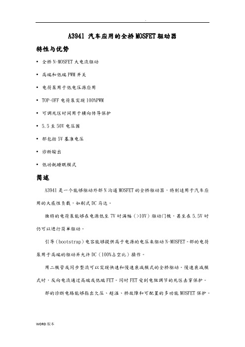
A3941 汽车应用的全桥MOSFET驱动器特性与优势•全桥N-MOSFET大电流驱动•高端和低端PWM开关•电荷泵用于低电压源应用•TOP-OFF电荷泵实现100%PWM•可调死区时间用于横向传导保护• 5.5至50V电压围•部包括5V基准电压•诊断输出•低功耗睡眠模式简述A3941是一个能够驱动外部N沟道MOSFET的全桥驱动器,特别适用于汽车应用的大感性负载,如刷式DC马达。
独特的电荷泵能够在电源低至7V时满幅(>10V)驱动门极,甚至在5.5V时仍可以进行简单驱动。
引导(bootstrap)电容能够提供高于电源的电压来驱动N-MOSFET。
部的电荷泵用于高端的驱动并允许DC(100%占空比)操作。
用二极管或同步整流可以实现快速和慢速衰减模式的全桥驱动。
慢速衰减模式时,反向电流通过高端或低端FET。
同时FET受到电阻调节的死区击穿保护。
部的诊断电路能够指出欠压、超温、桥故障和可配置的多功能MOSFET保护。
功能描述A3941是一种全桥MOSFET前置驱动器,单7至50V工作电源。
部包含一个5V 逻辑电压源。
4个高电流门驱动器有能力驱动宽围的N-MOSFET,它们被配置成2个高端驱动器和2个低端驱动器。
A3941包含必要的电路确保在电源低至7V时,FET的高端和低端(G-S)门极电压同时高于10V。
假如电压跌落,在5.5V时仍能保证正确的功能,但是会降低门极的驱动电压。
A3941可以被MCU输出的单路PWM信号驱动,并可被配置为快速或慢速衰减模式。
快速衰减可以提供4象限电机控制,而慢速衰减适合2象限地电机控制或者简单感性负载。
慢速衰减模式时,反向电流穿过高端或者低端MOSFET。
任何情况下,同步整流可以提高桥的效率。
外部桥击穿能够被可调死区避免。
低功耗睡眠模式允许A3941、桥和负载连接到车的电源上而不必外加电源开关。
A3941包括一些保护功能:欠压、超温和桥故障。
故障状态可以被MCU感知,它有2个故障输出端,FF1和FF2,可以提供给外部。
A3901中文资料
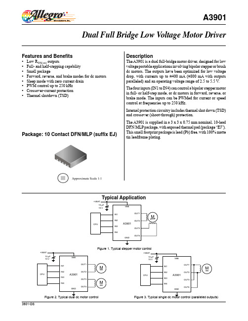
A3901
Dual Full Bridge Low Voltage Motor Driver
Features and Benefits
▪ Low RDS(on) outputs ▪ Full- and half-stepping capability ▪ Small package ▪ Forward, reverse, and brake modes for dc motors ▪ Sleep mode with zero current drain ▪ PWM control up to 250 kHz ▪ Crossover-current protection ▪ Thermal shutdown (TSD)
Dual Full Bridge Low Voltage Motor Driver
ELECTRICAL CHARACTERISTICS at TA =25°C, and VBB = 2.5 to 5.5 V, unless noted otherwise
Characteristics
Symbol
Test Conditions
Dual Full Bridge Low Voltage Motor Driver
10 µF 10 V
IN1
Functional Block Diagram
VBB
TSD
BRIDGE1 OUT1 OUT2
IN2 Control Logic and Gate Drive
IN3
IN4
BRIDGE2
OUT3 OUT4
DC Motor (Dual)
IN1 or IN3
IN2 or IN4
0
0
OFF OFF OFF OFF
UC3901在行波管收集极电源中的应用
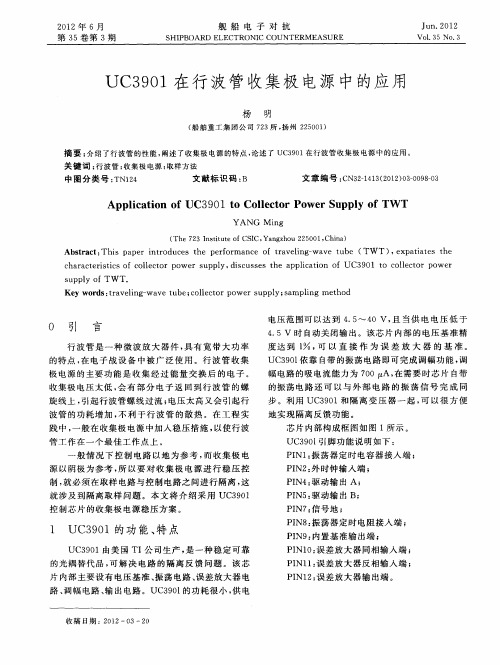
( e 7 3 I s i t fCS C, n z o 2 0 1 C i a Th 2 n t u e o I Ya g h u 2 5 0 , h n ) t
Ab t a t Thi p p r ntod e he e f ma c r v ln — v u sr c : s a e i r uc s t p ror n e of t a e i g wa e t be ( TW T ), x ta e t e e pa i t s h c r c e itc f c lc or po r s pp y, ic s s t pp i a i n o C39 1 O c le t r p we ha a t rs is o ole t we u l d s us e he a lc to f U 0 t o l c o o r s upp y o l fTW T. Ke r s: r vei — v ub c le t r p we u y wo d t a lng wa e t e; o l c o o r s ppl s mplng m e ho y; a i t d
器工 作频 率范 围宽 , 具有 振荡 器外部 同步功能 、 入 输
欠 电压锁 定 功 能 、 流 保 护 功 能 , 且 死 区 时 间 可 过 而 调 , 目前 比较 理 想的控 制器 。 是
取 样 原 理 如 图 2所 示 。
合 S 5 5实现 隔离反 馈稳 压 。 G3 2
图 2 隔离 取 样 原 理 图
UC 9 1的振 荡 器频 率理 论 上 可工 作至 兆赫 兹 30
级 , 高 的频率 有利 于减 少 隔 离 变压 器 的 匝数 和 尺 更 寸, 但较 高 的频 率 同时对 磁芯 等提 出 了更 高 的要 求 , 所 以在工 程实 践 中一般不 推荐 使用 到兆赫 兹级 。
S10040200P资料

SYMBOL
Vi Vov Tstg Tmb
PARAMETER
RF input voltage (single tone) DC supply over-voltage (5 minutes) storage temperature operating mounting base temperature
S10040200P
GaAs Push Pull Hybrid
40 – 1000MHz 20dB min. Gain @ 1000MHz
260mA max. @ 24VDC
MIN.
- 40 - 30
MAX.
75 30 + 100 + 100
UNIT
dBmV V °C °C
CHARACTERISTICS
19.5 20.0 0.5
-
TYP.
20.0
20.0
18.0
15.0
20.0
18.0
15.0
-
4.0
255.0
MAX.
20.5 21.5 1.5 ±0.4
4.5 260.0
UNIT
dB dB dB dB
dB dB dB dB dB dB dB mA
Notes: 1) The slope is defined as the difference between the gain at the start frequency and the gain at the stop frequency.
I U
123 5 789 C
E
M
R
J
S
P
K
O
T
øG
Q
N
草酰乙酸二乙酯生产工艺流程

草酰乙酸二乙酯生产工艺流程下载温馨提示:该文档是我店铺精心编制而成,希望大家下载以后,能够帮助大家解决实际的问题。
文档下载后可定制随意修改,请根据实际需要进行相应的调整和使用,谢谢!并且,本店铺为大家提供各种各样类型的实用资料,如教育随笔、日记赏析、句子摘抄、古诗大全、经典美文、话题作文、工作总结、词语解析、文案摘录、其他资料等等,如想了解不同资料格式和写法,敬请关注!Download tips: This document is carefully compiled by theeditor. I hope that after you download them,they can help yousolve practical problems. The document can be customized andmodified after downloading,please adjust and use it according toactual needs, thank you!In addition, our shop provides you with various types ofpractical materials,such as educational essays, diaryappreciation,sentence excerpts,ancient poems,classic articles,topic composition,work summary,word parsing,copy excerpts,other materials and so on,want to know different data formats andwriting methods,please pay attention!草酰乙酸二乙酯是一种重要的有机合成中间体,广泛应用于医药、农药、染料等领域。
ZDN3901便携式电能质量分析仪使用手册
ZDN3901便携式电能质量分析仪使用手册武汉智能星电气2021-2-20目录一、功能特点 (4)二、技术指标 (6)三、结构外观 (7)〔一〕、外型结构尺寸 (8)〔二〕、键盘分布 (9)四、液晶界面 (11) (24)〔一〕、三相四线制接线方式设备电参量的测量 (25)〔二〕、三相三线制接线方式设备电参量的测量 (26)〔三〕、波形显示测量局部 (27)〔四〕、频谱分析测量局部 (27)〔五〕、电压谐波分析局部 (28)〔六〕、电流谐波分析局部 (28)〔七〕、不平衡度测量局部 (29)六、电池维护及充电 (31)七、考前须知 (31)八、运输、贮存 (32)九、售后效劳 (32)ZDN3901 便携式电能质量分析仪电能质量是指通过公用电网供应用户端的交流电能的品质,通俗来说就是指电网线路中电能的好坏情况。
电能质量问题主要由终端负荷侧引起。
例如冲击性无功负载会使电网电压产生剧烈波动,降低供电质量。
随着电力电子技术的开展,它既给现代工业带来节能和能量变换积极的一面,同时电力电子装置在各行各业的广泛应用又对电能质量带来了新的更加严重的损害,已成为电网的主要谐波污染源。
电网系统中各个用户端配电网中使用的整流器、变频调速装置、电弧炉、电气化铁路以及各种电力电子设备不断增加。
给用电网络造成影响或者说是用电污染。
造成电压不稳、过电压、产生谐波等。
谐波使电能的生产、传输和利用的效率降低,使电气设备过热、产生振动和噪声,并使绝缘老化,寿命缩短,甚至发生故障或烧毁。
谐波还会引起电力系统局部发生并联谐振或串联谐振,使谐波含量被放大,致使电容器等设备烧毁。
这些负荷的非线性、冲击性和不平衡的用电特性,对供电质量造成严重污染。
因而消除供配电系统中的高次谐波问题对改善电能质量和确保电力系统平安、稳定、经济运行有着非常积极的意义。
另一方面,现代工业、商业及居民用户的用电设备对电能质量更加敏感,对供电质量提出了更高的要求。
供氧时间计算参考资料
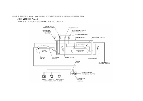
参考豪客及湾流机型AMM,AFM列出各机型氧气瓶安装情况及氧气可持续使用时间示意图:1. G550 机型/G550 AircraftG550配备2支氧气瓶(每支115cu ft,机组1支,乘客1支)(1) 氧气使用时间示意图(2) G550机队能力列表注:氧气使用时间为单支氧气瓶1800PSI压力下的总使用时间。
2. GV 机型GV配备2支氧气瓶(每支115cu ft,机组1支,乘客1支)(1) 氧气使用时间示意图(2) GV机队能力列表注:氧气使用时间为单支氧气瓶1800PSI压力下的总使用时间。
3. GIV 机型GIV配备4支氧气瓶。
参考附图。
B-8080,B-8082,B-8091配备的氧气瓶为:115*2立方英尺(旅客),50*2立方英尺(机组)。
B-8088配备的氧气瓶为:115*2立方英尺(旅客),115立方英尺(机组).FIG 1 适用于B-8080,B-8082,B-8091FIG2 适用于B-8088(1) 氧气使用时间示意图A. 对于B-8080,B-8082,B-8091飞机:起飞前氧气瓶压力为1800PSI(最大)时,15000英尺区域为机组持续供氧时间最低为2小时;B. 对于8088飞机,参考下图:当起飞前氧气瓶压力为1800PSI(最大)时,在15000英尺客舱高度情况下可以为机组持续供氧6小时左右。
(2) GIV机队能力列表注:氧气使用时间为单支氧气瓶1800PSI压力下的总使用时间.4. G450 机型G450配备2支氧气瓶(每支123cu ft,机组1 支,乘客1支)(1) 氧气使用时间示意图(2) G450机队能力列表5. G200 机型B-8083,8086,8089安装了两个77立方英尺的氧气瓶,B-8121安装了一个115立方英尺的氧气瓶。
(1) 氧气使用时间示意图(2) G200机队能力列表注:供氧时间根据图示按照2名机组+8名乘客计算。
6. HK4000 机型HK 4000 飞机配备了四个氧气瓶,2个标准的50立方英尺的氧气瓶,和2个22 立方英尺氧气瓶。
AS9000标准讲解PPT

7.2 与顾客有关的过程
组织应评审与产品有关的要求。评审应在组织向顾客作出 提供产品的承诺之前进行(如:提交标书、接受合同或 订单及接受合同或订单的更改),并应确保: a) 产品要求得到规定; b) 与以前表达不一致的合同或订单的要求已予解决; c) 组织有能力满足规定的要求;
d) 风险(如新技术、短交货期)得到评估。
标准和形成文件的程序之间的相互关系。 质量管理体系过程之间的相互作用的表述。
4.2.3文件控制
质量管理体系所要求的文件应予以控制。记录是一种特殊类 型的文件,应依据4.2.4的要求进行控制。 应编制形成文件的程序,以规定以下方面所需的控制: a) 文件分布前得到批准,以确保文件是充分与适宜的; b) 必要时对文件进行评审与更新,并再次批准; c) 确保文件的更改和现行修订状态得到识别; d) 确保在使用处可获得适用文件的有关版本; e) 确保文件保持清晰、易于识别; f) 确保外来文件得到识别,并控制其分发; g) 防止作废文件的非预期使用,若因任何原因而保留作废 文件时,对这些文件进行适当的标识。
质量管理体系
组织应按本标准的要求管理这些过程。 针对组织所选择的任何影响产品符合要求外包过 程,组织应确保对其实施控制。对此类外包过 程的控制应在质量管理体系中加以识别。 注:上述质量管理体系所需的过程应当包括与管 理活动、资源提供、产品实现和测量有关的过 程。
4.2 文件要求
4.2.1总则 质量管理体系文件应包括: a) 形成文件的质量方针和质量目标; b) 质量手册; c) 本标准所要求的形成文件的程序; d) 组织为确保其过程的有效策划、运行和控制所需的文 件; e) 本标准所要求的记录(见4.2.4);
AS9101标准讲义
热烈欢迎 安全事项 课程安排(时间、休息等) 注意事项(手机、纪律、提问等) 自我介绍
- 1、下载文档前请自行甄别文档内容的完整性,平台不提供额外的编辑、内容补充、找答案等附加服务。
- 2、"仅部分预览"的文档,不可在线预览部分如存在完整性等问题,可反馈申请退款(可完整预览的文档不适用该条件!)。
- 3、如文档侵犯您的权益,请联系客服反馈,我们会尽快为您处理(人工客服工作时间:9:00-18:30)。
AS3901ISM 433/315 MHz FSK/ASK Transmitter Data SheetRev. 06, August 2000Key Features•Supports the European 433 MHz ISM band.•No frequency pulling by (antenna) load variation due to PLL synthesizer.•Designed to be conform to EN 300 220-1 requirements.•Supports FSK (data rates 0…32 kb/s) or ASK modulation (data rates 0…20kb/s)•No data synchronization for FSK or ASK needed.•Supports clock and reset signals for the external µC.•Supports different power down modes, one without any running XTAL oscillator.•Wide supply range between 2.7 V to 5 V.•Only one XTAL and very few external elements required.•Wide operating temperature range from –40 C to +85 C.•Low TX current, typical 7 mA.General DescriptionThe AS3901 is a low power FSK/ (ASK) transmitter intended for the European 433 MHz and the US 315 MHz ISM band application. It uses a PLL stabilized oscillator whichavoids frequency pulling by approaching the antenna with objects as it occurs at SAW resonator based transmitters.FSK modulation is performed by an I/Q-based continuous phase FSK modulator with a well defined frequency deviation of 16 kHz. The FSK modulator is operating completely asynchronous to the TX data stream and therefore needs no data clock or other possible by switching the driving amplifier and FSK modulator on and off by an applied transmit data stream.The µC clock frequency and the FSK frequency deviation can be kept almost constant for both frequency bands by selecting the correct scaling factors by the 433/315 pin. As external components the AS3901 needs only a reference XTAL and 5 capacitors.Applications•Short range radio data transmission.•Remote keyless entry systems.•Security applications and alarm systems.•Domestic and consumer remote control units.•Remote metering.•Low power telemetry.This document contains information on products under development. Austria Mikro Systeme International AG reserves the right to change or discontinue this product without notice.1F u n c t i o n a l D e s c r i p t i o nThe AS3901 consists of a reference XTAL oscillator, a single channel RF- synthesizer, an I/Q based asynchronous continuos phase FSK modulator, a driving amplifier and a µC interface, including µC clock divider, and a power management circuitry.Figure 1: Block diagram of the AS3901.1.1RF SynthesizerThe RF synthesizer is a fully integrated single channel device with internal loop filter,generating the 433 MHz or 315 MHz transmit carrier frequency f RF by a fix, 32 times,multiplication of the reference XTAL frequency f XTAL.1.2Microprocessor ClockThe microprocesor clock frequency f CLK is generated by dividing the XTAL frequency f XTAL by 3 or 4, dependent on the 433/315 MHz selection pin to keep the µC clock frequencyf CLK almost constant for European and US applications.1.3ModulationThe FSK modulator is an I/Q modulator based continuos phase FSK modulator. Themodulating NRZ data may be in the range of 0 up to 32 kbit/s. The FSK frequencydeviation ∆f is ≈16 kHz, independent of the data rate. It is also kept almost constant for both transmit frequency bands by selecting proper frequency deviation multiplicationfactors of the XTAL reference frequency by the 433/315 MHz selection pin.The processing clock of the data source can be different from the AS3901 referenceXTAL or µC clock f CLK and no data synchronization of the FSK modulator is required.1.4Driving AmplifierThe driving amplifier has a differential open collector output optimized for driving ofsmall, symmetrical high-impedance loop antennas. The amplifier drives a nominal RFcurrent of 0.7 mA rms.The maximal differential voltage swing is about 4 V PP. Therefore the output power ist a function of the connected load impedance. With a 2 kΩ differentialload a nominal peak output power (to the antenna) of ≈1 mW is obtained. Please notethat the finally radiated power (from antenna) is lower and strongly dependent on theefficiency (function of the size) of the antenna to be used.1.5ASK ModulationASK modulation with a date rate upt to 20 kbits/s can be achieved by turning the driving amplifier and the FSK modulator by the TX/ASK pin on and off, where a TX/ASK = …H“means a turned on state.1.6Power Management and Operation ModesFor normal operation the switching between different operation modes follows a Grey-coded scheme to avoid unwanted switching between operation modes due to inaccurate occurrence of edges of STDBY and TX/ASK.Mode STDBY TX/ASK FunctionStandby11All OffClock generator operation10XTAL oscillator on and CLOCK outputactive.Transmit operation01XTAL oscillator, PLL, FSK modulatorrunning, (FSK operation or …H“transmittedat ASK).Turned off power00XTAL oscillator and PLL running, outputamplifier and FSK modulator off, (…L“transmitted at ASK).1.7µC Interface and TimingThe AS3901 contains a direct interface to a microcontroller (µC). The µC interface of the AS3901 consists of three input and two outputs pins:…Standby input“(STDBY).…Transmit / ASK input“(TX/ASK).…µC reset output (Active …L“)“(NRES).…µC clock output“(CLK).…FSK data input“(DATA).These lines support the µC with the required reset, clock and data signals. Lines 1 to 4 control the AS3901 internal power on/off circuit which wakes up and shuts down thewhole transmitter consisting of the AS3901 and the µC.Figure 2 shows a typical interconnection of the AS3901 with a typical µC. Figure 3presents a related timing for power up and down of the transmitter.AS3901STDBY DATA TX/ASK RESET NRES TX/ASK uCswitchSTDBY DATA CLKCLKFigure 2:Interconnection of the AS3901 with a typical µC.Note:At room temperature, resistor values of ≈10 k Ω are suggested for the µC interface.For other temperatures to be calculated from figure 5.TX/ASK CLK NRES STDBYFigure 3: µC interface timing for a transmission cycle.Note:Activating the transmit switch results in a …weak L state“ at TX/ASK. It can be overridden by the microcontroller so that the transmission cycle remains unaffected by the duration the switch is pressed. The STDBY and TX/ASK inputs have internal pullup resistors of ~100k Ω1.7.1Interface DescriptionWake-up sequence:TX/ASK=H, STDBY=H: Standby. All off low current state.TX/ASK→L, STDBY=H; → XTAL oscillator starts up. NRES goes L, resetting (starting) the µC for tXTON plus 3 clock cycles.NRES returns to H, µC initializes.After µC is initialized, it sets STDBY→L; PLL is turned on, after t PLLon a stable RF carrier is generated.TX/ASK→H, STDBY=L; →TX is turned on, t TXON later the RF signal is available and data can be transmitted.To switch the AS3901 …on“a …push button“with series resistance ~10-20 kΩ can beused to make TX/ASK = …L“. The …push-button“must be pushed long enough (typ. >3ms) for the µC to reset and sustain the TX/ASK …L“state.Standby procedure (for sleep-mode ( IDD1 <1µA):The µC outputs a …H“to TX/ASK and STDBY. After minimal 3 CLK cycles the XTALoscillator will be switched off. The pull-up resistors at the AS3901 TX/ASK and STDBY inputs will sustain the sleep mode.Note: Multiple …push buttons“for different functions can be used.2Electrical C h a r a c t e r i s t i c s2.1Absolute Maximum Ratings (non operating)Symbol Parameter Min Max Units Note VDD Positive supply voltage-0.57VGND Negative supply voltage00VV IN Voltage on input pins-0.5VDD+0.5VESD Electrostatic discharge1000V1) T STG Storage temperature-55125°CT LEAD Lead temperature260°C2) Note:1) HBM: R = 1.5 kΩ, C = 100 pF. The pins ANT1, ANT2, XTAL1 and XTAL2 have 500 V ESD protection.2) 260°C for 10 s (reflow and wave soldering), 360 °C for 3 s (manual soldering).2.2Operating ConditionsSymbol Parameter Min Typ Max Unit Note VDD Positive supply voltage 2.7 3.0 5.0VGND Negative supply voltage000V1µA1) IDD1Supply current,STDBY = ”H”, TX/ASK = ”H”IDD2Supply current,350850µA2) STDBY = ”H”, TX/ASK = ”L”79mA3) IDD3Supply current,STDBY = ”L”, TX/ASK = ”H”3.54.5mA4) IDD4Supply current,STDBY = ”L”, TX/ASK = ”L”T AMB Ambient temperature range-40+85°CNote:1) Standby:T AMB = 23 °C, Synthesizer and driving amplifier are turned off.2) Clock generator operation:T AMB = 23 °C XTAL oscillator and µC clock divider on. RF driving amplifier and PLL off, noexternal load connected to CLK pin.3)Transmit operation:T AMB = 23 °C, Synthesizer and driving amplifier are turned on.4)Turned off TX power:T AMB = 23 °C, XTAL oscillator and µC clock divider and PLL on RF driving amplifier off.2.3Transmit OperationT AMB = 23 °C, VDD = 3.0 V, unless specified otherwise.Symbol Parameter Conditions Min Typ Max Units Note f RF, EU Transmit frequency (Europe)f XTAL = 13.560 MHz433.920MHz1) f RF, US Transmit frequency (US)f XTAL = 9.84375 MHz315.000MHz1) f offset Frequency tolerance After t TXON, no XTALtolerance.2kHzf CLK, EUµC clock frequency (Europe)f XTAL = 13.560 MHz 3.390MHzf CLK, USµC clock frequency (US)f XTAL = 9.84375 MHz 3.28125MHzt TXon Transmitter turn on time FSK modulator anddriver amplifier20µst PLLon PLL turn on time t.b.d.msT XTon XTAL oscillator turn on time5msNote:1) XTAL tolerances will slightly change the typical transmit frequency.2.3.1 ASK OperationT AMB = 23 °C, VDD = 3.0 V, unless specified otherwise.Symbol Parameter Conditions Min Typ Max Units NoteP OUT,H Available peak outputpower In 2 kΩ, STDBY = ”L”,TX/ASK = ”H”-1.50 1.5dB m1) 3)P OUT,L Leakage peak outputpower In 2 kΩ, STDBY = ”L”,TX/ASK = ”L”-50dB mP OUT 3rd Radiated third harmonicoutput power Antenna attenuation>20 dB-39dB m2)P SP Spurious power In distance of f CLK orf XTAL from carrier. Noantenna selectivityassumed.-45-25dB C2) 3)R ASK ASK data rate range For a RF packet dutycycle ≥25 %.020Kb/sNote:1) Output power depends on load impedance, differential output current is typical 0.7 mA rms. Maximum differential voltage swingis typical 4 V PP.2) Measurement bandwidth (close to EN 300 220-1) see also figure 10.3) Actual E.R.P. depends on antenna efficiency2.3.2 FSK OperationT AMB = 23 °C, VDD = 3.0 V, unless specified otherwise.Symbol Parameter Conditions Min Typ Max Units NoteP OUT,FSK Available peak outputpower In 2 kΩ, STDBY = ”L”,TX/ASK = ”H”-1.50 1.5dB m1) 3)P OUT 3rd Radiated third harmonicoutput power Antenna and band passfilter attenuation> 20 dB-36dB m2)P SP Spurious power In distance of f CLK orf XTAL from carrier. Noantenna selectivityassumed.-45-25dB C2) 3)R FSK FSK data rate range032kb/s4)∆f FSK frequency deviation16kHzNote:1) Output power depends on load impedance, differential output current is typical 0.7 mA ms. Maximum differential voltageswing is typical 4 V PP.2) Measurement bandwidth (close to EN 300 220-1) see also figure 10.3) Actual E.R.P. depends on antenna efficiency4) Guaranteed by design2.4Digital Pin CharacteristicsT AMB = 23 °C, VDD = 3.0 V, unless specified otherwise. GND is the 0 V reference.Symbol Parameter Conditions Min Typ Max Units Note CLK (µC clock output)VOH High level output voltage IOH = -1 mA VDD-0.7-VDD VVOL Low level output voltage IOL = 1 mA GND- 1.2Vtr Rise time CLoad = 10 pF20nstd Fall time CLoad = 10 pF20nsjcc Cycle to cycle jitter+/-5%1) NRES (Inverted reset output)VOH High level output voltage IOH = -1 mA VDD-0.3-VDD VVOL Low level output voltage IOL = 1 mA GND-0.2Vtr Rise time CLoad = 10 pF20nstd Fall time CLoad = 10 pF20nsTX/ASK (Driving amplifier and FSK modulator on/off (ASK) input)VIH High level input voltage VDD-0.5-VDD VVIL Low level input voltage GND-0.3VIIH High level input current VIH = VDD1-40µA IIL Low level input current VIL = 0 V.internal pull-upDATA (FSK data input)VIH High level input voltage VDD-0.5-VDD VVIL Low level input voltage GND-0.3VIIH High level input current VIH = VDD1µAIIL Low level input current VIL = 0 V-1µA433/315 (Band selection (division ratio))VIH High level input voltage VDD-0.5-VDD V VIL Low level input voltage GND-0.3V IIH High level input current VIH = VDD1µA IIL Low level input current VIL = 0 V.-1µA STANDBY (Standby input)VIH High level input voltage VDD-0.5VDD V VIL Low level input voltage GND-0.3V IIH High level input current VIH = VDD1µA-40µA 1IIL Low level input current VIL = 0 V.internal pull-upNotes1) Guaranteed by design3P i n-o u t I n f o r m a t i o nPin #Pin Name Input / Output Description1STDBY Dig. Input, 100 kΩ pull up Power down for all functions 2CLK Dig. Output Clock output (CMOS level)3DATA Dig. Input Transmit data input (CMOS level)4TX/ASKon/off ASK Dig. Input, 100 kΩ pull up Power off for TX (PLL and XTAL working)ASK modulation5GND Power Ground6VDD Power Positive supply (2.7 V-5.0 V)7XTAL2Analog XTAL pin28XTAL1Analog XTAL pin19433/315Dig. Input Selects division factors for constant µCClock frequency and deviation10VDDRF Power Positive supply (2.7 V-5.0 V)11ANT2Analog open collector output To loop antenna12ANT1Analog open collector output To loop antenna13GNDRF Power Ground14NRESET Dig. Output Reset, …L“state resets a microcontroller4A p p l i c a t i o n S c h e m a t i c3PC5Figure 4:Basic application schematic of the AS3901.Figure 5:Pull Up characteristics for the TX/ASK pin.5Typical MeasurementsFigure 6:Narrow band output spectrum of the AS3901 FSK modulated with pseudoclose to the EN 300-220-1 recommendation for wide-band equipment, clause 8.6.Instead of 5 kHz video bandwidth (VBW) 10 kHz was used. The markers were setup to the band edges. (433.050 MHz, 434.790 MHz) The recommendation saysthat the spectrum should be observed at least 1MHz form the ISM band edges, butit was measured with larger frequency span.Figure 8:Modulation bandwidth of the AS3901 in AKS operation at 9.2 kbit/s, measured close to the EN 300-220-1 recommendatio for wide-band equipment, clause 8.6.Instead of 5 kHz video bandwidth (VBW) 10 kHz was used. The markers were setup to the band edges. (433.050 MHz, 434.790 MHz) The recommendation saysthat the spectrum should be observed at least 1 MHz from the ISM band edges,Figure 9:1Recommendation for wide-band equipment, clause 8.7, without modulation. (Onlydifference: 100 kHz RBW was used instead of 120 kHz). From the measurement it can beseen that the main critical spurious emission is generated by the 13.56 MHz clock frequency.The level of CLK spurious is near –48 dBM so the suppression is 45 dB for this component.Figure 10:Typical out spectrum in ASK 9.2 kb/s PRN modulation.Figure 11:Transmission power as function of time at ASK modulation with an 9.2 kbit/s 0101.. data pattern.6P a c k a g e I n f o r m a t i o nFigure 12:Physical dimensions of TSSOP-14.Common DimensionsSymbolMinimal (mm)Nominal (mm)Maximal (mm) A-- 1.20A10.05-0.15b0.19-0.30D 4.90- 5.10e0.65 BSCE- 6.40-E1 4.30- 4.50L0.45-0.75α0°-8°Copyright © 2000, Austria Mikro Systeme International AG, Schloß Premstätten, 8141 Unterpremstätten, Austria.Tel.: +43-(0)3136-500-0, Fax: +43-(0)3136-52501, E-Mail: info@All rights reserved. No part of this publication may be reproduced, stored in a retrieval system, or transmitted, in any form or by any means, without the prior permission in writing by the copyright holder. To the best of its knowledge, Austria Mikro Systeme International asserts that the information contained in this publication is accurate and correct.。
