BT151F-650中文资料
F650终

第二节 C201指示灯介绍
下面介绍C201的LED指示灯。
指示灯
LED1
定义
事故总跳闸
源
(接点输出F_03)OR(接点输出G_03)OR(虚拟输出 011)OR(相欠电压1运行)OR(F_06接点输出)OR(LED2)
LED2
LED3 LED4 LED5 LED6 LED7 LED8 LED9 LED10 LED11 LED12 LED13 LED14 LED15
瞬时速断过流 (速断) 反时限过流保护 负序速断 负序过流 低电压跳C201 灵敏接地方向 灵敏接地过流保 护 辅助过电压
26.2A 19S
44A 0S IP=5A 2IP=1.5S 5A 0.1S 2.7A 1.5S 45V 3S 45° 正向 0.033A 0.1S 40V
相IOC2高定值运行
相IOC1高定值运行 相TOC1高定值运行 负序TOC1运行 负序TOC2运行 相欠电压1运行 灵敏接地方向1运行 灵敏接地IOC1运行 辅助过电压1运行
OR
LED1
LED1
AND
G_01断开
保护动作闭锁开车回路
第五节 C201F650的控制功能
C201用以控制的接点有F_08和G_02,现分别介绍。 F_08:C201故障跳闸连锁跳氨鼓风机
LED1 F_08输出闭合
AND
连锁跳氨鼓风机
G_02:低油压启动辅助油泵
F15输入
AND
G_02闭合
启动辅助油泵
问答?
• 1、C201电机保护包括( ),( ),( ), ( ),( )。 • 2、C201和( ),( )之间有连锁。 • 3、简述C201电气故障保护跳氨鼓风机原理。 答案:1、速断/过流,欠压,接地保护,工艺故障,氨鼓风 机连锁跳C201。 2、氨鼓风机和辅助油泵。 3、C201输出接点F_08与中间继电器1ZJ串联接入 110V直流电源,中间继电器引一副常闭接点到C202氨鼓风 机控制回路,与接触器线圈串联。当C201保护动作时,输 出接点F_08闭合,中间继电器线圈带电,辅助接点断开, C202氨鼓风机接触器线圈失电,氨鼓风机跳闸。
F650技术规范指南
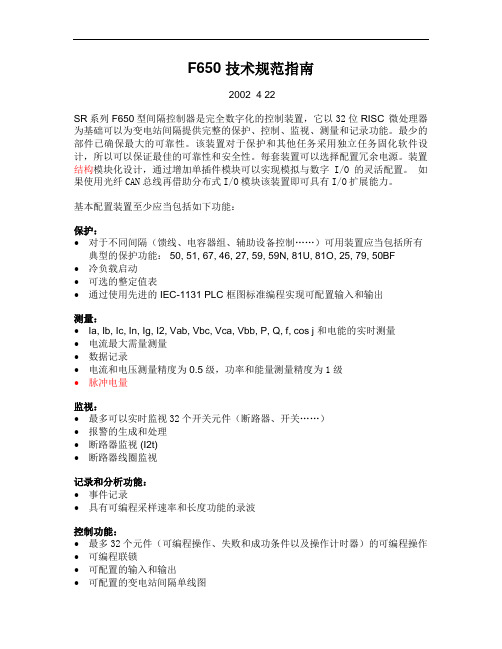
F650 技术规范指南2002 4 22SR系列F650型间隔控制器是完全数字化的控制装置,它以32位RISC 微处理器为基础可以为变电站间隔提供完整的保护、控制、监视、测量和记录功能。
最少的部件已确保最大的可靠性。
该装置对于保护和其他任务采用独立任务固化软件设计,所以可以保证最佳的可靠性和安全性。
每套装置可以选择配置冗余电源。
装置结构模块化设计,通过增加单插件模块可以实现模拟与数字I/O的灵活配置。
如果使用光纤CAN总线再借助分布式I/O模块该装置即可具有I/O扩展能力。
基本配置装置至少应当包括如下功能:保护:•对于不同间隔(馈线、电容器组、辅助设备控制……)可用装置应当包括所有典型的保护功能: 50, 51, 67, 46, 27, 59, 59N, 81U, 81O, 25, 79, 50BF•冷负载启动•可选的整定值表•通过使用先进的 IEC-1131 PLC 框图标准编程实现可配置输入和输出测量:•Ia, Ib, Ic, In, Ig, I2, Vab, Vbc, Vca, Vbb, P, Q, f, cos j 和电能的实时测量•电流最大需量测量•数据记录•电流和电压测量精度为0.5级,功率和能量测量精度为1级•脉冲电量监视:•最多可以实时监视32个开关元件(断路器、开关……)•报警的生成和处理•断路器监视 (I2t)•断路器线圈监视记录和分析功能:•事件记录•具有可编程采样速率和长度功能的录波控制功能:•最多32个元件(可编程操作、失败和成功条件以及操作计时器)的可编程操作•可编程联锁•可配置的输入和输出•可配置的变电站间隔单线图HMI 和通讯:•用于保护运行数据显示的就地 4行 x 20字符 LCD•可选择配置的用于间隔信息显示的图形 LCD (128x240 像素或16 x 40字符) 应至少包括如下内容的用户可编程屏幕:o单线图显示o开关操作o访问测量信息o报警屏幕显示o调试用I/O状态显示•前部 RS232 通讯端口•后部冗余 RS485 或塑料光纤或玻璃光纤的异步端口•后部以太网10/100 Base T同步端口•可选择配置的100 Base F光纤,单配置或冗余配置同步端口。
BT152-600中文资料

J
2.4
K5.0L Nhomakorabea2.2
M
1.25
N
0.45
O
0.6
φ
3.6
Max. 10.1 6.7 9.47 13.3 1.4
3.4 1.4 2.7 5.15 2.6 1.55 0.6 1.0
Min. 0.382 0.248 0.354 0.504 0.047
0.118 0.049 0.094 0.197 0.087 0.049 0.018 0.024
V
─
20
mA
VGT
Gate Trigger Voltage (2)
VD = 6 V(DC), RL=10 Ω
TC = 25 °C
─
─
1.5
V
VGD
Non-Trigger Gate Voltage (1) VAK = 12 V, RL=100 Ω
TC = 125 °C
0.2
─
─
V
dv/dt
Critical Rate of Rise Off-State Linear slope up to VD=VDRM 67%,
元器件交易网 SemiWell Semiconductor
Preliminary
BT152-600
Silicon Controlled Rectifiers
Features
◆ Repetitive Peak Off-State Voltage : 600V ◆ R.M.S On-State Current ( IT(RMS)= 20 A ) ◆ Low On-State Voltage (1.4V(Typ.)@ ITM) ◆ Non-iosolated Type
GE综保F650中文简介

监视和测量故障测距、最后10次记录断路器跳闸和失灵VT 断线断路器总拉弧电流事件记录-479次事件高分辨率录波和数据记录,采样速率可编程设置测量:V ,I ,Hz ,W ,VA ,PF需量:Ia ,Ib ,Ic ,Ig ,Isg ,I2,MW ,MVA 可配置图形人机接口报警显示前面板配备往复键,4x20个字节的背光显示屏幕或16x40个字节的可选择的图形显示屏幕RS232和RS485接口-速率可达115,200 bps以太网接口-10/100BaseTX ,100BaseFX 带ST 接头,可选的带ST 接头的双100BaseFX ,用于物理介质冗余多规约-ModBus TM RTU 和TCP/IP DNP 3.0级别2,IEC 60870-5-104,IEC 61850,Http ,ftp 和tftpEnerVista 软件-处于工业系统领先地位的软件工具,与GE Multilin 设备一起使用,简化工作过程的每一个方面用户接口保护和控制完整的延时、瞬时和相方向、中性点、接地和灵敏接地过电流不同线路中的负序延时过流断线检测相延时过流的电压制动母线和线路辅助压欠压/过电压中性点过电压负序电压母线欠频率/过频率断路器失灵由PLC 控制的带冷负荷启动的手动合闸可配置的四次重合闸3个定值设置组同期检查-V ,φ和Hz 多达32个可编程数字输入多达16个数字输出跳闸回路监视冗余电源选择可编程逻辑高成本效益的信息访问-通过多规约、标准RS232、RS485和以太网端口通过开放式标准规约达到最佳化的集成灵活性-Modbus RTU 和TCP/IP ,DNP 3.0级别2,IEC 60870-5-104,IEC 61850与标准internet 浏览器兼容-通过规约,例如Http ,ftp 和tftp最大程度地缩短通讯中断时间-配备10/100BaseTX 的可靠冗余以太网通讯端口,100BaseFX 配备ST 接头,可选择的双100BaseFX 也配备ST 接头完备的监视功能-包括需量和电能在内的详尽测量功能跟随技术发展-用于产品现场升级的闪存技术独特的嵌入式控制功能-综合馈线保护加可编程逻辑对于复杂系统的灵活性和高成本效率的控制-使用符合IEC 标准的可编程逻辑自定义馈线保护和控制系统的功能,满足独特的要求一流的人机接口(HMI)-4 x 20标准背光式LCD 显示,可选择16 x 40(240x128像素)图形LCD ,配备可编程按钮和选择设置菜单及子菜单的旋转开关更换时间最小化-模块化设计,插件可抽出结构减少故障排除时间和降低维护成本-IRIG-B 时间同步、事件报告、波形捕捉、数据记录配电线路和母联的管理和主保护母线、变压器和输电线路的后备保护可靠的配电发电互联保护系统和中低压电动机保护主要优点馈线/间隔保护系统保护、控制、监视、分析和电能计量系统应用特性保护和控制F650提供用于馈线管理和间隔控制的快速保护和控制,保护功能包括:过流保护瞬时和延时过流功能可用于相、中性点、接地/灵敏接地,延时过流功能可用于负序电流。
BT151-800R中文资料
50
100
150
Tj / C
Fig.7. Normalised gate trigger current IGT(Tj)/ IGT(25˚C), versus junction temperature Tj.
IL(Tj) IL(25 C) 3
BT145
2.5
2
1.5
1
0.5
0 -50
Fig.8.
0
50
IT(RMS) / A 15 10
BT151
109 C
5
0-50
0
50
100
150
Tmb / C
Fig.3. Maximum permissible rms current IT(RMS) , versus mounting base temperature Tmb.
ITSM / A 120 100
September 1997
3
Rev 1.200
元器件交易网
Philips Semiconductors
Thyristors
Product specification
BT151 series
IGT(Tj) 3 IGT(25 C)
BT151
2.5
2
1.5
1
0.5
0
-50
0
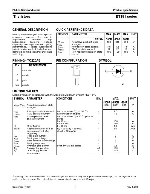
domestic lighting, heating and static
switching.
QUICK REFERENCE DATA
SYMBOL PARAMETER
MAX. MAX. MAX. UNIT
VDRM, VRRM IT(AV) IT(RMS) ITSM
BT151- 500R 650R 800R
BT151-650R中文资料
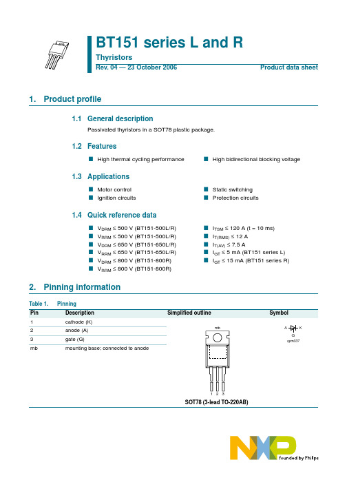
1.Product profile1.1General descriptionPassivated thyristors in a SOT78 plastic package.1.2Features1.3Applications1.4Quick reference data2.Pinning informationBT151 series L and RThyristorsRev. 04 — 23 October 2006Product data sheetI High thermal cycling performanceI High bidirectional blocking voltageI Motor control I Static switching I Ignition circuitsI Protection circuitsI V DRM ≤500V (BT151-500L/R)I I TSM ≤120A (t =10ms)I V RRM ≤500V (BT151-500L/R)I I T(RMS)≤12A I V DRM ≤650V (BT151-650L/R)I I T(AV)≤7.5AI V RRM ≤650V (BT151-650L/R)I I GT ≤5mA (BT151 series L)I V DRM ≤800V (BT151-800R)II GT ≤15mA (BT151 series R)IV RRM ≤800V (BT151-800R)Table 1.PinningPin Description Simplified outline Symbol1cathode (K)SOT78 (3-lead TO-220AB)2anode (A)3gate (G)mbmounting base; connected to anode12mb3sym037AKG3.Ordering information4.Limiting values[1]Although not recommended,off-state voltages up to 800V may be applied without damage,but the thyristor may switch to the on-state.The rate of rise of current should not exceed 15A/µs.Table 2.Ordering informationType numberPackage NameDescriptionVersion BT151-500L SC-46plastic single-ended package; heatsink mounted; 1 mounting hole;3-lead TO-220ABSOT78BT151-500R BT151-650L BT151-650R BT151-800RTable 3.Limiting valuesIn accordance with the Absolute Maximum Rating System (IEC 60134).Symbol ParameterConditionsMin Max Unit V DRMrepetitive peak off-state voltageBT151-500L; BT151-500R [1]-500V BT151-650L; BT151-650R [1]-650V BT151-800R-800V V RRMrepetitive peak reverse voltageBT151-500L; BT151-500R [1]-500V BT151-650L; BT151-650R [1]-650V BT151-800R-800V I T(AV)average on-state current half sine wave; T mb ≤109°C;see Figure 1-7.5A I T(RMS)RMS on-state current all conduction angles;see Figure 4and 5-12AI TSMnon-repetitive peak on-state currenthalf sine wave; T j =25°C prior to surge; see Figure 2and 3t =10ms -120A t =8.3ms-132A I 2t I 2t for fusingt =10ms-72A 2s dI T /dt rate of rise of on-state current I TM =20A; I G =50mA;dI G /dt =50 mA/µs-50A/µs I GM peak gate current -2A V RGM peak reverse gate voltage -5V P GM peak gate power -5W P G(AV)average gate power over any 20ms period -0.5W T stg storage temperature −40+150°C T jjunction temperature-125°CForm factor a =I T(RMS)/I T(AV)Fig 1.Total power dissipation as a function of average on-state current; maximum valuesf =50HzFig 2.Non-repetitive peak on-state current as a function of the number of sinusoidal current cycles; maximumvaluesI T(AV) (A)8642001aaa95851015P tot (W)0118.5112105.5T mb(max)(°C)125a =1.5742.82.21.9conduction angle (degrees)form factor a 30609012018042.82.21.91.57α001aaa9578040120160 I TSM (A)0n110310210t pT j initial = 25 °C max I TI TSMtt p ≤10msFig 3.Non-repetitive peak on-state current as a function of pulse width for sinusoidal currents;maximum valuesf =50Hz; T mb ≤109°CFig 4.RMS on-state current as a function of surgeduration; maximum values Fig 5.RMS on-state current as a function of mountingbase temperature; maximum values001aaa956t p (s)10−510−210−310−4102103I TSM (A)10dl T /dt limitt pT j initial = 25 °C maxI TI TSMt surge duration (s)10−210110−1001aaa954101552025I T(RMS)(A)0T mb (°C)−50150100050001aaa999841216I T(RMS)(A)5.Thermal characteristicsTable 4.Thermal characteristics Symbol ParameterConditions Min Typ Max Unit R th(j-mb)thermal resistance from junction to mounting basesee Figure 6-- 1.3K/W R th(j-a)thermal resistance from junction to ambientin free air-60-K/WFig 6.Transient thermal impedance from junction to mounting base as a function of pulse width001aaa96210−110−2110Z th(j-mb)(K/W)10−3t p (s)10−511010−110−210−410−3t pt p TPtTδ =6.CharacteristicsTable 5.CharacteristicsT j = 25°C unless otherwise stated.Symbol Parameter Conditions Min Typ Max Unit Static characteristicsI GT gate trigger current V D=12V; I T=100mA; see Figure8BT151-500L-25mABT151-500R-215mABT151-650L-25mABT151-650R-215mABT151-800R-215mA I L latching current V D=12V; I GT=100mA; seeFigure10-1040mAI H holding current V D=12V; I GT=100mA; seeFigure11-720mA V T on-state voltage I T=23A; see Figure9- 1.4 1.75VV GT gate trigger voltage I T=100mA; V D=12V; see Figure7-0.6 1.5VI T=100mA; V D=V DRM(max);T j=125°C0.250.4-VI D off-state current V D=V DRM(max); T j=125°C-0.10.5mA I R reverse current V R=V RRM(max); T j=125°C-0.10.5mA Dynamic characteristicsdV D/dt rate of rise of off-statevoltage V DM=0.67× V DRM(max); T j=125°C;exponential waveform; see Figure12R GK=100Ω2001000-V/µs gate open circuit50130-V/µst gt gate-controlled turn-ontime I TM=40A; V D=V DRM(max);I G=100mA; dI G/dt=5A/µs-2-µst q commutated turn-offtime V DM=0.67× V DRM(max); T j=125°C;I TM=20A; V R=25V;(dI T/dt)M=30A/µs; dV D/dt=50V/µs;R GK=100Ω-70-µsFig 7.Normalized gate trigger voltage as a function ofjunction temperatureFig 8.Normalized gate trigger current as a function ofjunction temperatureV o =1.06V R s =0.0304Ω(1)T j =125°C; typical values (2)T j =125°C; maximum values (3)T j =25°C; maximum valuesFig 9.On-state current as a function of on-statevoltage Fig 10.Normalized latching current as a function ofjunction temperatureT j (°C)−50150100050001aaa9530.81.21.60.4V GT V GT(25°C)T j (°C)−50150100050001aaa9521230I GT I GT(25°C)V T (V)021.50.51001aaa959102030I T (A)0(3)(2)(1)T j (°C)−50150100050001aaa9511230I L I L(25°C)(1) R GK =100Ω(2) Gate open circuitFig 11.Normalized holding current as a function ofjunction temperatureFig 12.Critical rate of rise of off-state voltage as afunction of junction temperature; minimum valuesT j (°C)−50150100050001aaa950123I H I H(25°C)0001aaa949103102104dV D /dt (V/µs)10T j (°C)015010050(2)(1)7.Package outlineFig 13.Package outline SOT78 (TO-220AB)REFERENCESOUTLINE VERSION EUROPEAN PROJECTIONISSUE DATE IECJEDEC JEITA SOT78SC-463-lead TO-220ABDD 1qpL123L 1b 1e eb0510 mmscalePlastic single-ended package; heatsink mounted; 1 mounting hole; 3-lead TO-220ABSOT78DIMENSIONS (mm are the original dimensions)A E A 1cQL 2UNIT A 1b 1D 1e p mm2.54q Q A b D c L 2max.3.03.83.515.012.83.302.793.02.72.62.20.70.416.015.20.90.61.451.004.74.11.401.256.65.910.39.7L 1E L 05-03-2205-10-25mounting base8.Revision historyTable 6.Revision historyDocument ID Release date Data sheet status Change notice SupersedesBT151_SER_L_R_420061023Product data sheet-BT151_SERIES_3 Modifications:•The format of this data sheet has been redesigned to comply with the new identityguidelines of NXP Semiconductors.•Legal texts have been adapted to the new company name where appropriate.•Added type numbers BT151-500L and BT151-650LBT151_SERIES_320040607Product specification-BT151_SERIES_2 (939775013159)BT151_SERIES_219990601Product specification-BT151_SERIES_1 BT151_SERIES_119970901Product specification--BT151_SER_L_R_4© NXP B.V . 2006. All rights reserved.Product data sheet Rev. 04 — 23 October 200611 of 129.Legal information9.1Data sheet status[1]Please consult the most recently issued document before initiating or completing a design.[2]The term ‘short data sheet’ is explained in section “Definitions”.[3]The product status of device(s)described in this document may have changed since this document was published and may differ in case of multiple devices.The latest product status information is available on the Internet at URL .9.2DefinitionsDraft —The document is a draft version only. The content is still under internal review and subject to formal approval, which may result in modifications or additions. NXP Semiconductors does not give any representations or warranties as to the accuracy or completeness ofinformation included herein and shall have no liability for the consequences of use of such information.Short data sheet —A short data sheet is an extract from a full data sheet with the same product type number(s)and title.A short data sheet is intended for quick reference only and should not be relied upon to contain detailed and full information. For detailed and full information see the relevant full data sheet, which is available on request via the local NXP Semiconductors sales office. In case of any inconsistency or conflict with the short data sheet, the full data sheet shall prevail.9.3DisclaimersGeneral —Information in this document is believed to be accurate andreliable.However,NXP Semiconductors does not give any representations or warranties,expressed or implied,as to the accuracy or completeness of such information and shall have no liability for the consequences of use of such information.Right to make changes —NXP Semiconductors reserves the right to make changes to information published in this document, including withoutlimitation specifications and product descriptions, at any time and without notice.This document supersedes and replaces all information supplied prior to the publication hereof.Suitability for use —NXP Semiconductors products are not designed,authorized or warranted to be suitable for use in medical, military, aircraft,space or life support equipment, nor in applications where failure ormalfunction of a NXP Semiconductors product can reasonably be expected to result in personal injury, death or severe property or environmental damage.NXP Semiconductors accepts no liability for inclusion and/or use of NXP Semiconductors products in such equipment or applications and therefore such inclusion and/or use is at the customer’s own risk.Applications —Applications that are described herein for any of these products are for illustrative purposes only. NXP Semiconductors makes no representation or warranty that such applications will be suitable for the specified use without further testing or modification.Limiting values —Stress above one or more limiting values (as defined in the Absolute Maximum Ratings System of IEC 60134)may cause permanent damage to the device.Limiting values are stress ratings only and operation of the device at these or any other conditions above those given in theCharacteristics sections of this document is not implied. Exposure to limiting values for extended periods may affect device reliability.Terms and conditions of sale —NXP Semiconductors products are sold subject to the general terms and conditions of commercial sale,as published at /profile/terms , including those pertaining to warranty,intellectual property rights infringement and limitation of liability, unless explicitly otherwise agreed to in writing by NXP Semiconductors. In case of any inconsistency or conflict between information in this document and such terms and conditions, the latter will prevail.No offer to sell or license —Nothing in this document may be interpreted or construed as an offer to sell products that is open for acceptance or the grant,conveyance or implication of any license under any copyrights,patents or other industrial or intellectual property rights.9.4TrademarksNotice:All referenced brands,product names,service names and trademarks are the property of their respective owners.10.Contact informationFor additional information, please visit:For sales office addresses, send an email to:salesaddresses@Document status [1][2]Product status [3]DefinitionObjective [short] data sheet Development This document contains data from the objective specification for product development.Preliminary [short] data sheet Qualification This document contains data from the preliminary specification.Product [short] data sheetProductionThis document contains the product specification.11.Contents1Product profile. . . . . . . . . . . . . . . . . . . . . . . . . . 11.1General description. . . . . . . . . . . . . . . . . . . . . . 11.2Features . . . . . . . . . . . . . . . . . . . . . . . . . . . . . . 11.3Applications . . . . . . . . . . . . . . . . . . . . . . . . . . . 11.4Quick reference data. . . . . . . . . . . . . . . . . . . . . 12Pinning information. . . . . . . . . . . . . . . . . . . . . . 13Ordering information. . . . . . . . . . . . . . . . . . . . . 24Limiting values. . . . . . . . . . . . . . . . . . . . . . . . . . 25Thermal characteristics. . . . . . . . . . . . . . . . . . . 56Characteristics. . . . . . . . . . . . . . . . . . . . . . . . . . 67Package outline . . . . . . . . . . . . . . . . . . . . . . . . . 98Revision history. . . . . . . . . . . . . . . . . . . . . . . . 109Legal information. . . . . . . . . . . . . . . . . . . . . . . 119.1Data sheet status . . . . . . . . . . . . . . . . . . . . . . 119.2Definitions. . . . . . . . . . . . . . . . . . . . . . . . . . . . 119.3Disclaimers. . . . . . . . . . . . . . . . . . . . . . . . . . . 119.4T rademarks. . . . . . . . . . . . . . . . . . . . . . . . . . . 1110Contact information. . . . . . . . . . . . . . . . . . . . . 1111Contents. . . . . . . . . . . . . . . . . . . . . . . . . . . . . . 12Please be aware that important notices concerning this document and the product(s)described herein, have been included in section ‘Legal information’.© NXP B.V.2006.All rights reserved.For more information, please visit: For sales office addresses, please send an email to: salesaddresses@Date of release: 23 October 2006Document identifier: BT151_SER_L_R_4。
BT151中文资料_数据手册_参数

SYMBOL PARAMETER
CONDITIONS
MIN.
VDRM, VRRM Repetitive peak off-state
-
voltages
IT(AV) IT(RMS) ITSM
I2t dIT/dt IGM VGM VRGM PGM PG(AV) Tstg Tj
Average on-state current half sine wave; Tmb ≤ 109 ˚C
IL(Tj) IL(25 C) 3
BT145
2.5
2
1.5
1
0.5
0 -50
Fig.8.
0
50
100
150
Tj / C
Normalised latching current IL(Tj)/ IL(25˚C), versus junction temperature Tj.
IH(Tj) IH(25 C) 3
currents, f = 50 Hz; Tmb ≤ 109˚C.
VGT(Tj) 1.6 VGT(25 C)
BT151
1.4
1.2
1
0.8
0.6
0.4-50
0
50
100
150
Tj / C
Fig.6. Normalised gate trigger voltage VGT(Tj)/ VGT(25˚C), versus junction temperature Tj.
September 1997
3
Rev 1.200
Philips Semiconductors
Thyristors
Product specification
BTA151中文资料
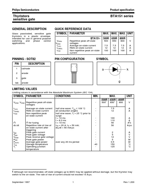
Thyristors BTA151 seriessensitive gateGENERAL DESCRIPTIONQUICK REFERENCE DATAGlass passivated,sensitive gate SYMBOL PARAMETERMAX.MAX.MAX.UNIT thyristors in a plastic envelope,intended for use in general purpose BTA151-500R 650R 800R switching and phase control V DRM ,Repetitive peak off-state 500650800V applications.V RRM voltagesI T(AV)Average on-state current 7.57.57.5A I T(RMS)RMS on-state current121212A I TSMNon-repetitive peak on-state 100100100AcurrentPINNING - SOT82PIN CONFIGURATION SYMBOLLIMITING VALUESLimiting values in accordance with the Absolute Maximum System (IEC 134).SYMBOLPARAMETERCONDITIONSMIN.MAX.UNIT -500R -650R -800R V DRM , V RRM Repetitive peak off-state-50016501800V voltages I T(AV)Average on-state current half sine wave; T mb ≤ 109 ˚C -7.5A I T(RMS)RMS on-state current all conduction angles-12A I TSMNon-repetitive peak half sine wave; T j = 25 ˚C prior to on-state currentsurge t = 10 ms -100A t = 8.3 ms -110A I 2t I 2t for fusingt = 10 ms-50A 2s dI T /dt Repetitive rate of rise of I TM = 20 A; I G = 50 mA;-50A/µs on-state current after dI G /dt = 50 mA/µstriggeringI GM Peak gate current -2A V GM Peak gate voltage-5V V RGM Peak reverse gate voltage -12V P GM Peak gate power -5W P G(AV)Average gate power over any 20 ms period -0.5W T stg Storage temperature -40150˚C T jOperating junction -125˚Ctemperature1 Although not recommended, off-state voltages up to 800V may be applied without damage, but the thyristor may switch to the on-state. The rate of rise of current should not exceed 15 A/µs.THERMAL RESISTANCESSYMBOL PARAMETERCONDITIONSMIN.TYP.MAX.UNIT R th j-mb Thermal resistance-- 1.3K/W junction to mounting base R th j-aThermal resistance in free air -60-K/Wjunction to ambientSTATIC CHARACTERISTICST j = 25 ˚C unless otherwise stated SYMBOL PARAMETER CONDITIONSMIN.TYP.MAX.UNIT I GT Gate trigger current V D = 12 V; I T = 0.1 A -24mA I L Latching current V D = 12 V; I GT = 0.1 A -1040mA I H Holding current V D = 12 V; I GT = 0.1 A -716mA V T On-state voltage I T = 23 A- 1.4 1.75V V GT Gate trigger voltage V D = 12 V; I T = 0.1 A-0.6 1.5V V D = V DRM(max); I T = 0.1 A; T j = 125 ˚C 0.250.4-V I D , I ROff-state leakage currentV D = V DRM(max); V R = V RRM(max); T j = 125 ˚C-0.10.5mADYNAMIC CHARACTERISTICST j = 25 ˚C unless otherwise stated SYMBOL PARAMETER CONDITIONSMIN.TYP.MAX.UNITdV D /dtCritical rate of rise of V D = 67% V DRM(max); T j = 125 ˚C;off-state voltage exponential waveformGate open circuit50130-V/µs R GK = 100 Ω2001000-V/µs t gt Gate controlled turn-on I TM = 40 A; V D = V DRM ; I G = 0.1 A;-2-µs timedI G /dt = 5 A/µst qCircuit commutated V D = 67% V DRM(max); I TM = 20 A; V R = 25 V;-70-µsturn-off timedI TM /dt = 30 A/µs; dV D /dt = 50 V/µs;R GK = 100 ΩMECHANICAL DATA1. Refer to mounting instructions for SOT82 envelopes.2. Epoxy meets UL94 V0 at 1/8".DEFINITIONSData sheet statusObjective specification This data sheet contains target or goal specifications for product development. Preliminary specification This data sheet contains preliminary data; supplementary data may be published later. Product specification This data sheet contains final product specifications.Limiting valuesLimiting values are given in accordance with the Absolute Maximum Rating System (IEC 134). Stress above one or more of the limiting values may cause permanent damage to the device. These are stress ratings only and operation of the device at these or at any other conditions above those given in the Characteristics sections of this specification is not implied. Exposure to limiting values for extended periods may affect device reliability. Application informationWhere application information is given, it is advisory and does not form part of the specification.© Philips Electronics N.V. 1997All rights are reserved. Reproduction in whole or in part is prohibited without the prior written consent of the copyright owner.The information presented in this document does not form part of any quotation or contract, it is believed to be accurate and reliable and may be changed without notice. No liability will be accepted by the publisher for any consequence of its use. Publication thereof does not convey nor imply any license under patent or other industrial or intellectual property rights.LIFE SUPPORT APPLICATIONSThese products are not designed for use in life support appliances, devices or systems where malfunction of these products can be reasonably expected to result in personal injury. Philips customers using or selling these products for use in such applications do so at their own risk and agree to fully indemnify Philips for any damages resulting from such improper use or sale.。
f650a参数

f650a参数F650A是一款具有高性能和多功能的机械设备,广泛应用于工业生产领域。
本文将从多个角度介绍F650A的参数及其应用。
F650A的主要参数包括功率、转速、负载能力等方面。
F650A拥有强大的功率输出,能够满足大部分工业生产的需求。
其高转速特性使得设备运行更加稳定,能够提高生产效率。
此外,F650A具备较高的负载能力,能够承受较大的工作压力,保证设备的安全运行。
F650A还具有多种功能和特点。
首先,F650A采用先进的控制系统,能够实时监测设备运行状态,并根据实际情况进行调整,保证设备的稳定性和安全性。
在实际应用中,F650A有着广泛的适用性。
首先,F650A常用于工业生产线上,用于各种物料的搬运、装载和运输。
其高负载能力和稳定性使得设备能够胜任重物料的运输工作,提高生产效率。
其次,F650A还可以应用于仓储物流行业,用于货物的装卸和堆垛。
其灵活的工作模式和自动化操作功能使得设备能够适应不同的仓储需求,并提高工作效率。
此外,F650A还可以应用于建筑工地和港口码头等领域,用于各种工程施工和物料运输工作。
除了以上应用领域,F650A还具备一定的环境适应性。
它可以在室内和室外环境下正常工作,能够适应不同的气候条件和工作环境。
此外,F650A还具备一定的防尘和防水性能,能够在恶劣的工作条件下正常运行,保证设备的稳定性和安全性。
F650A作为一款具有高性能和多功能的机械设备,在工业生产领域有着广泛的应用。
其强大的功率输出、高转速特性和大负载能力使得设备能够胜任各种重型工作任务。
同时,其先进的控制系统、多种工作模式和自动化操作功能保证了设备的稳定性、灵活性和高效性。
无论是在工业生产线上还是在仓储物流行业,F650A都能够发挥出其优秀的性能和功能,提高生产效率,满足各种生产需求。
可控硅型号参数BT
PHILIPS 体继电器、相位控 0.6 制和小功率交流电 风扇速度控制 逻辑电平可控硅, 用于通用开关、固
600
BT1308-400D
PHILIPS 体继电器、相位控 0.8 制和小功率交流电 风扇速度控制
400
逻辑电平可控硅, 用于通用开关、固 BT1308-600D PHILIPS 体继电器、相位控 0.8 制和小功率交流电 风扇速度控制 逻辑电平可控硅, 用于通用开关、固 BT131 系列 PHILIPS 体继电器、相位控 1 制和小功率交流电 风扇速度控制 逻辑电平可控硅, 用于通用开关、固 BT132 系列 PHILIPS 体继电器、相位控 1 制和小功率交流电 风扇速度控制 可控硅,用于通用 开关、 固体继电器、 BT134 系列 PHILIPS 相位控制和小功率 4 交流电风扇速度控 制 可控硅,用于通用 开关、 固体继电器、 BT136-500 PHILIPS 相位控制和小功率 4 交流电风扇速度控 制 可控硅,用于通用 开关、 固体继电器、 BT136-500D PHILIPS 相位控制和小功率 4 交流电风扇速度控 制 可控硅,用于通用 开关、 固体继电器、 BT136-500E PHILIPS 相位控制和小功率 4 交流电风扇速度控 制 可控硅,用于通用 开关、 固体继电器、 BT136-500F PHILIPS 相位控制和小功率 4 交流电风扇速度控 制 可控硅,用于通用 BT136-500G PHILIPS 开关、 固体继电器、 4 相位控制和小功率 50m 1.5 70m 1.5 25m 1.5 10m 1.5 70m 1.5 500-800 500-600 0.4 0.7 500-600 600
可控硅,用于通用 开关、 固体继电器、 BT139-600G PHILIPS 相位控制和小功率 16 交流电风扇速度控 制 可控硅,用于通用 开关、 固体继电器、 BT139-800 PHILIPS 相位控制和小功率 16 交流电风扇速度控 制 可控硅,用于通用 开关、 固体继电器、 BT139-800E PHILIPS 相位控制和小功率 16 交流电风扇速度控 制 可控硅,用于通用 开关、 固体继电器、 BT139-800F PHILIPS 相位控制和小功率 16 交流电风扇速度控 制 可控硅,用于通用 开关、 固体继电器、 BT139 系列 PHILIPS 相位控制和小功率 16 交流电风扇速度控 制 可控硅,用于通用 开关、 固体继电器、 BT145 系列 PHILIPS 相位控制和小功率 16 交流电风扇速度控 制 可控硅,用于通用 开关、 固体继电器、 BT148 系列 PHILIPS 相位控制和小功率 2.5 交流电风扇速度控 制 逻辑电平可控硅, 用于通用开关、固 BT149A PHILIPS 体继电器、相位控 制和小功率交流电 风扇速度控制 逻辑电平可控硅, BT149B PHILIPS 用于通用开关、固 体继电器、相位控 200m 200m 400-600 500-800 500-800 25m 1.5 10m 1.5 35m 1.5 50m 1.5
BT151S-500R
Philips SemiconductorsProduct specificationThyristors BT151S seriesBT151M seriesGENERAL DESCRIPTIONQUICK REFERENCE DATAGlass passivated thyristors in a plastic SYMBOL PARAMETERMAX.MAX.MAX.UNIT envelope,suitable for surface mounting,intended for use in BT151S (or BT151M)-500R 650R 800R applications requiring high V DRM ,Repetitive peak off-state 500650800V bidirectional blocking voltage V RRM voltagescapability and high thermal cycling I T(AV)Average on-state current 7.57.57.5A performance.Typical applications I T(RMS)RMS on-state current121212A include motor control,industrial and I TSMNon-repetitive peak on-state 100100100Adomestic lighting,heating and static currentswitching.PINNING - SOT428PIN CONFIGURATIONSYMBOLLIMITING VALUESLimiting values in accordance with the Absolute Maximum System (IEC 134).SYMBOLPARAMETERCONDITIONSMIN.MAX.UNIT -500R -650R -800R V DRM , V RRM Repetitive peak off-state-50016501800V voltages I T(AV)Average on-state current half sine wave; T mb ≤ 103 ˚C-7.5A I T(RMS)RMS on-state current all conduction angles-12A I TSMNon-repetitive peak half sine wave; T j = 25 ˚C prior to on-state currentsurge t = 10 ms -100A t = 8.3 ms -110A I 2t I 2t for fusingt = 10 ms-50A 2s dI T /dt Repetitive rate of rise of I TM = 20 A; I G = 50 mA;-50A/µs on-state current after dI G /dt = 50 mA/µstriggeringI GM Peak gate current -2A V GM Peak gate voltage-5V V RGM Peak reverse gate voltage -5V P GM Peak gate power -5W P G(AV)Average gate power over any 20 ms period -0.5W T stg Storage temperature -40150˚C T jOperating junction -125˚Ctemperature1 Although not recommended, off-state voltages up to 800V may be applied without damage, but the thyristor may switch to the on-state. The rate of rise of current should not exceed 15 A/µs.查询BT151S-500R供应商THERMAL RESISTANCESSYMBOL PARAMETERCONDITIONSMIN.TYP.MAX.UNIT R th j-mb Thermal resistance-- 1.8K/W junction to mounting base R th j-aThermal resistance pcb (FR4) mounted; footprint as in Fig.14-75-K/Wjunction to ambientSTATIC CHARACTERISTICST j = 25 ˚C unless otherwise stated SYMBOL PARAMETER CONDITIONSMIN.TYP.MAX.UNIT I GT Gate trigger current V D = 12 V; I T = 0.1 A -215mA I L Latching current V D = 12 V; I GT = 0.1 A -1040mA I H Holding current V D = 12 V; I GT = 0.1 A -720mA V T On-state voltage I T = 23 A- 1.4 1.75V V GT Gate trigger voltage V D = 12 V; I T = 0.1 A-0.6 1.5V V D = V DRM(max); I T = 0.1 A; T j = 125 ˚C 0.250.4-V I D , I ROff-state leakage currentV D = V DRM(max); V R = V RRM(max); T j = 125 ˚C-0.10.5mADYNAMIC CHARACTERISTICST j = 25 ˚C unless otherwise stated SYMBOL PARAMETER CONDITIONSMIN.TYP.MAX.UNITdV D /dtCritical rate of rise of V DM = 67% V DRM(max); T j = 125 ˚C;off-state voltage exponential waveform;Gate open circuit50130-V/µs R GK = 100 Ω2001000-V/µs t gt Gate controlled turn-on I TM = 40 A; V D = V DRM(max); I G = 0.1 A;-2-µs timedI G /dt = 5 A/µst qCircuit commutated V D = 67% V DRM(max); T j = 125 ˚C;-70-µsturn-off timeI TM = 20 A; V R = 25 V; dI TM /dt = 30 A/µs;dV D /dt = 50 V/µs; R GK = 100 ΩMECHANICAL DATAMOUNTING INSTRUCTIONSNotes1. Plastic meets UL94 V0 at 1/8".DEFINITIONSData sheet statusObjective specification This data sheet contains target or goal specifications for product development. Preliminary specification This data sheet contains preliminary data; supplementary data may be published later. Product specification This data sheet contains final product specifications.Limiting valuesLimiting values are given in accordance with the Absolute Maximum Rating System (IEC 134). Stress above one or more of the limiting values may cause permanent damage to the device. These are stress ratings only and operation of the device at these or at any other conditions above those given in the Characteristics sections of this specification is not implied. Exposure to limiting values for extended periods may affect device reliability. Application informationWhere application information is given, it is advisory and does not form part of the specification.© Philips Electronics N.V. 1997All rights are reserved. Reproduction in whole or in part is prohibited without the prior written consent of the copyright owner.The information presented in this document does not form part of any quotation or contract, it is believed to be accurate and reliable and may be changed without notice. No liability will be accepted by the publisher for any consequence of its use. Publication thereof does not convey nor imply any license under patent or other industrial or intellectual property rights.LIFE SUPPORT APPLICATIONSThese products are not designed for use in life support appliances, devices or systems where malfunction of these products can be reasonably expected to result in personal injury. Philips customers using or selling these products for use in such applications do so at their own risk and agree to fully indemnify Philips for any damages resulting from such improper use or sale.Copyright © Each Manufacturing Company.All Datasheets cannot be modified without permission.This datasheet has been download from :100% Free DataSheet Search Site.Free Download.No Register.Fast Search System.。
英飞凌系列场效应管参数表

N沟道小功率20V-800V型号BSR202NBSR802NBSS205NBSS214NBSS806NBSS806NEBSS816NWBSS214NWBSD214SNBSD816SNBSD235NBSD840NBSL202SNBSL802SNBSL205NBSL207NBSL214NBSL806NBSR302NBSS306NBSS316NBSD316SNBSL302SNBSL306NBSS670S2LBSR606NBSP295 BSP318S 2N7002 BSS138N BSS7728N SN7002N SN7002W BSS138W 2N7002DW BSS606N BSL606SN BSP716N BSP123 BSP373 BSP372 BSP296N BSP372N BSP373N BSP296 BSS123N BSS119N BSP297 BSP88 BSP89 BSS131 BSS87 BSP298BSP299 BSP125 BSS127 BSS225 BSP300数据手册下载地址:80/dgdl/Infineon-BSR202N-DS-v01_09-en.pdf?folderId=db3a3043156fd573011622e10b5c1f67&fileId=db3a3043156fd573011622e5576e1f72:80/dgdl/Infineon-BSR802N-DS-v01_00-en.pdf?folderId=db3a3043156fd573011622e10b5c1f67&fileId=db3a30431b0626df011b129302297bc1:80/dgdl/Infineon-BSS205N-DS-v02_04-en.pdf?folderId=db3a3043156fd573011622e10b5c1f67&fileId=db3a304330f686060131091244950062:80/dgdl/Infineon-BSS214N-DS-v02_03-en.pdf?folderId=db3a3043156fd573011622e10b5c1f67&fileId=db3a304330f6860601311828a70444e9:80/dgdl/Infineon-BSS806N-DS-v02_03-en.pdf?folderId=db3a3043156fd573011622e10b5c1f67&fileId=db3a304330f686060131185f0553451c:80/dgdl/Infineon-BSS806NE-DS-v02_01-en.pdf?folderId=db3a3043156fd573011622e10b5c1f67&fileId=db3a304340f610c201410d1548de3366:80/dgdl/Infineon-BSS816NW-DS-v02_03-en.pdf?folderId=db3a3043156fd573011622e10b5c1f67&fileId=db3a304335113a6301351e704a2e1332 :80/dgdl/Infineon-BSS214NW-DS-v02_02-en.pdf?folderId=db3a3043156fd573011622e10b5c1f67&fileId=db3a30431b3e89eb011b695aebc01bde :80/dgdl/Infineon-BSD214SN-DS-v02_04-en.pdf?folderId=db3a3043156fd573011622e10b5c1f67&fileId=db3a30431add1d95011b01d1628230a0 :80/dgdl/Infineon-BSD816SN-DS-v02_05-en.pdf?folderId=db3a3043156fd573011622e10b5c1f67&fileId=db3a30431b0626df011b12af48627bf1:80/dgdl/BSD235N_Rev2+5.pdf?folderId=db3a3043156fd573011622e10b5c1f67&fileI d=db3a30431add1d95011afc70075c04e0:80/dgdl/BSD840N_Rev2+4.pdf?folderId=db3a3043156fd573011622e10b5c1f67&fileI d=db3a30431b0626df011b12b4486c7c02:80/dgdl/Infineon-BSL202SN-DS-v02_00-en.pdf?folderId=db3a3043156fd573011622e10b5c1f67&fileId=db3a3043156fd573011622e191d41f68:80/dgdl/Infineon-BSL802SN-DS-v01_00-en.pdf?folderId=db3a3043156fd573011622e10b5c1f67&fileId=db3a30431b0626df011b129ef9177bd1:80/dgdl/Infineon-BSL205N-DS-v02_03-en.pdf?folderId=db3a3043156fd573011622e10b5c1f67&fileId=db3a304342c787030142d7cdfb924d8d:80/dgdl/Infineon-BSL207N-DS-v02_03-en.pdf?folderId=db3a3043156fd573011622e10b5c1f67&fileId=db3a30431add1d95011aee15c15b0376 :80/dgdl/Infineon-BSL214N-DS-v02_03-en.pdf?folderId=db3a3043156fd573011622e10b5c1f67&fileId=db3a30431add1d95011afc5baa4504c2:80/dgdl/Infineon-BSL806N-DS-v02_03-en.pdf?folderId=db3a3043156fd573011622e10b5c1f67&fileId=db3a30431b0626df011b128dcbe37bb1:80/dgdl/Infineon-BSR302N-DS-v01_03-en.pdf?folderId=db3a3043156fd573011622e10b5c1f67&fileId=db3a3043156fd573011622e789f21f7c:80/dgdl/Infineon-BSS306N-DS-v02_03-en.pdf?folderId=db3a3043156fd573011622e10b5c1f67&fileId=db3a304330f686060130ff4c1f867ef5:80/dgdl/BSS316N_Rev2.3.pdf?folderId=db3a3043156fd573011622e10b5c1f67&fileId =db3a304330f686060130ff7ee4b07f16:80/dgdl/Infineon-BSD316SN-DS-v02_04-en.pdf?folderId=db3a3043156fd573011622e10b5c1f67&fileId=db3a30431add1d95011afc90c46a0521:80/dgdl/Infineon-BSL302SN-DS-v02_00-en.pdf?folderId=db3a3043156fd573011622e10b5c1f67&fileId=db3a3043156fd573011622e9b2061f88:80/dgdl/Infineon-BSL306N-DS-v02_04-en.pdf?folderId=db3a3043156fd573011622e10b5c1f67&fileId=db3a30431add1d95011afc80323d04f0:80/dgdl/Infineon-BSS670S2L-DS-v02_06-en.pdf?folderId=db3a3043156fd573011622e10b5c1f67&fileId=db3a304330f68606013109e4a7fb0094:80/dgdl/Infineon-BSR606N-DS-v02_03-en.pdf?folderId=db3a3043156fd573011622e10b5c1f67&fileId=db3a30433e78ea82013e7ea9a659062ben.pdf?folderId=db3a3043156fd573011622e10b5c1f67&fileId=db3a30433b47825b013b515cf1f42949:80/dgdl/Infineon-BSP295-DS-v02_03-en.pdf?folderId=db3a3043156fd573011622e10b5c1f67&fileId=db3a30433b47825b013b5fc5eed1573f:80/dgdl/Infineon-BSP318S-DS-v02_04-en.pdf?folderId=db3a3043156fd573011622e10b5c1f67&fileId=db3a30433b47825b013b51c9a6fc2aa8:80/dgdl/Infineon-2N7002-DS-v02_04-en.pdf?folderId=db3a3043156fd573011622e10b5c1f67&fileId=db3a304319bc939a0119c2a9461e79e6 :80/dgdl/Infineon-BSS138N-DS-v02_86-en.pdf?folderId=db3a3043156fd573011622e10b5c1f67&fileId=db3a304330f68606013104d944d53efb:80/dgdl/Infineon-BSS7728N-DS-v02_05-en.pdf?folderId=db3a3043156fd573011622e10b5c1f67&fileId=db3a304330f686060131184c5bf6450b:80/dgdl/Infineon-SN7002N-DS-v02_06-en.pdf?folderId=db3a3043156fd573011622e10b5c1f67&fileId=db3a304330f6860601311934e76045d5 :80/dgdl/Infineon-SN7002W-DS-v02_05-en.pdf?folderId=db3a3043156fd573011622e10b5c1f67&fileId=db3a3043344adb9d0134569a59ab6195 :80/dgdl/Infineon-BSS138W-DS-v02_43-en.pdf?folderId=db3a3043156fd573011622e10b5c1f67&fileId=db3a304335113a6301351e62fcb4131f:80/dgdl/2N7002DW_Rev2+3.pdf?folderId=db3a3043156fd573011622e10b5c1f67&fil eId=db3a30431a5c32f2011ad94ed41363f2:80/dgdl/Infineon-BSS606N-DS-v02_02-en.pdf?folderId=db3a3043156fd573011622e10b5c1f67&fileId=db3a30433dfcb54c013dfd4f43ed0120:80/dgdl/Infineon-BSL606SN-DS-v02_02-en.pdf?folderId=db3a3043156fd573011622e10b5c1f67&fileId=db3a30433c6c52e2013c6ca13340015f:80/dgdl/Infineon-BSP716N-DS-v02_00-en.pdf?folderId=db3a3043156fd573011622e10b5c1f67&fileId=db3a304341c1e4a10141da580f3529e9:80/dgdl/Infineon-BSP123-DS-v01_05-en.pdf?folderId=db3a304412b407950112b408e8c90004&fileId=db3a304412b407950112b42f29634b0b :80/dgdl/Infineon-BSP373-DS-v02_00-en.pdf?folderId=db3a304412b407950112b408e8c90004&fileId=db3a304412b407950112b42f38674b1b :80/dgdl/Infineon-BSP372-DS-v02_00-en.pdf?folderId=db3a304412b407950112b408e8c90004&fileId=db3a304412b407950112b42f18d64af7 :80/dgdl/Infineon-BSP296N-DS-v02_00-en.pdf?folderId=db3a3043156fd573011622e10b5c1f67&fileId=db3a30433dd58def013dd5af675d001f:80/dgdl/Infineon-BSP372N-DS-v02_00-en.pdf?folderId=db3a3043156fd573011622e10b5c1f67&fileId=db3a30433dd58def013dd8e68ae413f6:80/dgdl/Infineon-BSP373N-DS-v02_00-en.pdf?folderId=db3a3043156fd573011622e10b5c1f67&fileId=db3a30433dd58def013dd8fc3bcf143f:80/dgdl/Infineon-BSP296-DS-v02_01-en.pdf?folderId=db3a3043156fd573011622e10b5c1f67&fileId=db3a304340cdf0fd0140e3364cc72bd5:80/dgdl/Infineon-BSS123N-DS-v02_03-en.pdf?folderId=db3a3043156fd573011622e10b5c1f67&fileId=db3a304335f1f4b6013639adfaaa1631:80/dgdl/Infineon-BSS119N-DS-v02_01-en.pdf?folderId=db3a3043156fd573011622e10b5c1f67&fileId=db3a304335f1f4b6013639b6532a164a:80/dgdl/Infineon-BSP297-DS-v02_02-en.pdf?folderId=db3a3043156fd573011622e10b5c1f67&fileId=db3a30433b47825b013b51250a8528c2 :80/dgdl/Infineon-BSP88-DS-v02_02-en.pdf?folderId=db3a3043156fd573011622e10b5c1f67&fileId=db3a30433b47825b013b4b657acf0ca8:80/dgdl/Infineon-BSP89-DS-v02_02-en.pdf?folderId=db3a3043156fd573011622e10b5c1f67&fileId=db3a30433b47825b013b4b8a07f90d55 :80/dgdl/Infineon-BSS131-DS-v02_06-en.pdf?folderId=db3a3043156fd573011622e10b5c1f67&fileId=db3a304330f68606013104bf65993eeb:80/dgdl/Infineon-BSS87-DS-v01_42-en.pdf?folderId=db3a3043156fd573011622e10b5c1f67&fileId=db3a30433b47825b013b60b6e9436ddb :80/dgdl/Infineon-BSP298-DS-v02_06-en.pdf?folderId=db3a3043156fd573011622e10b5c1f67&fileId=db3a30433b47825b013b4c05f65f0f29en.pdf?folderId=db3a3043156fd573011622e10b5c1f67&fileId=db3a30433b47825b013b4c38c51e0fe9 :80/dgdl/Infineon-BSP299-DS-v02_04-en.pdf?folderId=db3a3043156fd573011622e10b5c1f67&fileId=db3a30433b47825b013b4c60b78c104c :80/dgdl/Infineon-BSP125-DS-v02_02-en.pdf?folderId=db3a3043156fd573011622e10b5c1f67&fileId=db3a30433b47825b013b50cae9702806 :80/dgdl/Infineon-BSS127-DS-v02_01-en.pdf?folderId=db3a3043156fd573011622e10b5c1f67&fileId=db3a304330f686060131049ef4883edb :80/dgdl/Infineon-BSS225-DS-v01_27-en.pdf?folderId=db3a3043156fd573011622e10b5c1f67&fileId=db3a30433b47825b013b60c128d06dfa :80/dgdl/Infineon-BSP300-DS-v02_02-en.pdf?folderId=db3a3043156fd573011622e10b5c1f67&fileId=db3a30433b47825b013b4c980bd0110d报价 €/1K封装耐压极性内阻0.12SC5920.0 V-21.0 mOhm 0.13SC5920.0 V-23.0 mOhm 0.05SOT-2320.0 V-85.0 mOhm 0.04SOT-2320.0 V-250.0 mOhm 0.05SOT-2320.0 V-57.0 mOhm 0.05SOT-2320.0 V N57.0 mOhm 0.04SOT-32320.0 V-160.0 mOhm 0.04SOT-32320.0 V-250.0 mOhm 0.05SOT-36320.0 V-250.0 mOhm 0.04SOT-36320.0 V--0.05SOT-36320.0 V-600.0 mOhmdual0.04SOT-36320.0 V-400.0 mOhmdual0.15TSOP-620.0 V N36.0 mOhm 0.15TSOP-620.0 V N22.0 mOhm20.0 V N85.0 mOhm 0.14TSOP-6dual0.14TSOP-620.0 V N110.0 mOhmdual0.12TSOP-620.0 V N250.0 mOhmdual-TSOP-620.0 V-57.0 mOhmdual0.13SC5930.0 V-23.0 mOhm 0.06SOT-2330.0 V-57.0 mOhm 0.04SOT-2330.0 V-160.0 mOhm 0.05SOT-36330.0 V-160.0 mOhm 0.15TSOP-630.0 V N25.0 mOhm30.0 V N57.0 mOhm 0.14TSOP-6dual0.04SOT-2355.0 V-650.0 mOhm 0.13SC5960.0 V N60.0 mOhm0.23SOT-22360.0 V N300.0 mOhm 0.19SOT-22360.0 V N90.0 mOhm0.02SOT-2360.0 V-3,000.0 mOhm 0.02SOT-2360.0 V-3,500.0 mOhm 0.03SOT-2360.0 V-5,000.0 mOhm 0.02SOT-2360.0 V-5,000.0 mOhm 0.02SOT-32360.0 V-5,000.0 mOhm 0.03SOT-32360.0 V-3,500.0 mOhm60.0 V-3,000.0 mOhm 0.03SOT-363dual0.12SOT-8960.0 V N60.0 mOhm0.11TSOP-660.0 V N60.0 mOhm0.11SOT-22375.0 V N160.0 Ohm-SOT-223100.0 V N6,000.0 mOhm -SOT-223100.0 V N300.0 mOhm-SOT-223100.0 V N310.0 mOhm 0.23SOT-223100.0 V N600.0 mOhm 0.21SOT-223100.0 V N230.0 mOhm 0.23SOT-223100.0 V N240.0 mOhm-SOT-223100.0 V N700.0 mOhm 0.03SOT-23100.0 V-6,000.0 mOhm 0.08SOT-23100.0 V-6,000.0 mOhm 0.21SOT-223200.0 V N1,800.0 mOhm 0.15SOT-223240.0 V N600.0 mOhm 0.16SOT-223240.0 V N6,000.0 mOhm 0.06SOT-23240.0 V-14,000.0 mOhm 0.16SOT-89240.0 V N6,000.0 mOhm 0.39SOT-223400.0 V N3,000.0 mOhm0.39SOT-223500.0 V N4,000.0 mOhm 0.28SOT-223600.0 V N45,000.0 mOhm 0.04SOT-23600.0 V-500,000.0 mOhm 0.16SOT-89600.0 V N45,000.0 mOhm 0.37SOT-223800.0 V N20,000.0 mOhm。
F650介绍
F650馈线/间隔保护系统性能总括 F650馈线/ 馈线
• • • • •
实用于任何电压等级的馈线与间隔保护和控制 界面友好的可视化整定、测量、监测和编程软件 就地操作配置往复式旋钮和可选择的图形界面 模块化的设计便于更换内部模块 通过RS232、RS485与以太网端口进行通讯
——无锡科环自动化设备有限公司 无锡科环自动化设统 保护、控制、监测、分析和电能计量系统
• • • • • • • • • • • 独特的嵌入式控制功能 对于复杂系统的灵活性和高成本效率的控制 一流的人机接口 更换时间最小化 减少故障排除时间和降低维护成本 高成本效益的信息访问 通过开放式标准规约达到最佳化的集成灵活性 与标准Internet浏览器兼容 最大程度的缩短通讯中断时间 完备的监视功能 跟随技术发展
F650扫描方式
读入输入
保护原理由内部扫描实现: 保护原理由内部扫描实现: 保护原理
逻辑计算
PKP DPO OP
输出
电源模块: 电源模块: • 宽阔的输入范围(LO 24-28V DC;HI 110-250V DC 110-270V AC) • 大于80%的高效功耗 • 可选的双电源模块
CPU模块与通讯模块: 模块与通讯模块: 模块与通讯模块 • • • • • 32位高速RICS CPU,具有超过32兆字节的存储与大于50MIPS的强大功能 通过最大速度的主线可以实现高速的信号处理 强大的闪存功能可以轻松实现升级 标准组件的即插即用功能 高速的通讯功能(10/100Mbps 的以太网通讯、RS485总线通讯以及RS232串口通讯)
用户接口
• 前面板配往复键,4×20个字符的背光显示屏幕或16 ×40个字符的可选择图形显示屏幕 • RS232和RS485接口-速率可达115,220bps • 以太网接口-10/100BaseTX,100BaseFX带ST接头可选 的带ST接头的双100BaseFX用于物理介质冗余 • 多规约-ModBus RTU和TCP/IP DNP3.0级别2、 IEC60870-5-104,IEC61850,http、ftp、tftp • Enervista软件-处于工业系统领先地位的软件工具,与 GE Multilin设备一起使用,简化工作过程的每一个方面
GE综保F650中文简介
监视和测量故障测距、最后10次记录断路器跳闸和失灵VT 断线断路器总拉弧电流事件记录-479次事件高分辨率录波和数据记录,采样速率可编程设置测量:V ,I ,Hz ,W ,VA ,PF需量:Ia ,Ib ,Ic ,Ig ,Isg ,I2,MW ,MVA 可配置图形人机接口报警显示前面板配备往复键,4x20个字节的背光显示屏幕或16x40个字节的可选择的图形显示屏幕RS232和RS485接口-速率可达115,200 bps以太网接口-10/100BaseTX ,100BaseFX 带ST 接头,可选的带ST 接头的双100BaseFX ,用于物理介质冗余多规约-ModBus TM RTU 和TCP/IP DNP 3.0级别2,IEC 60870-5-104,IEC 61850,Http ,ftp 和tftpEnerVista 软件-处于工业系统领先地位的软件工具,与GE Multilin 设备一起使用,简化工作过程的每一个方面用户接口保护和控制完整的延时、瞬时和相方向、中性点、接地和灵敏接地过电流不同线路中的负序延时过流断线检测相延时过流的电压制动母线和线路辅助压欠压/过电压中性点过电压负序电压母线欠频率/过频率断路器失灵由PLC 控制的带冷负荷启动的手动合闸可配置的四次重合闸3个定值设置组同期检查-V ,φ和Hz 多达32个可编程数字输入多达16个数字输出跳闸回路监视冗余电源选择可编程逻辑高成本效益的信息访问-通过多规约、标准RS232、RS485和以太网端口通过开放式标准规约达到最佳化的集成灵活性-Modbus RTU 和TCP/IP ,DNP 3.0级别2,IEC 60870-5-104,IEC 61850与标准internet 浏览器兼容-通过规约,例如Http ,ftp 和tftp最大程度地缩短通讯中断时间-配备10/100BaseTX 的可靠冗余以太网通讯端口,100BaseFX 配备ST 接头,可选择的双100BaseFX 也配备ST 接头完备的监视功能-包括需量和电能在内的详尽测量功能跟随技术发展-用于产品现场升级的闪存技术独特的嵌入式控制功能-综合馈线保护加可编程逻辑对于复杂系统的灵活性和高成本效率的控制-使用符合IEC 标准的可编程逻辑自定义馈线保护和控制系统的功能,满足独特的要求一流的人机接口(HMI)-4 x 20标准背光式LCD 显示,可选择16 x 40(240x128像素)图形LCD ,配备可编程按钮和选择设置菜单及子菜单的旋转开关更换时间最小化-模块化设计,插件可抽出结构减少故障排除时间和降低维护成本-IRIG-B 时间同步、事件报告、波形捕捉、数据记录配电线路和母联的管理和主保护母线、变压器和输电线路的后备保护可靠的配电发电互联保护系统和中低压电动机保护主要优点馈线/间隔保护系统保护、控制、监视、分析和电能计量系统应用特性保护和控制F650提供用于馈线管理和间隔控制的快速保护和控制,保护功能包括:过流保护瞬时和延时过流功能可用于相、中性点、接地/灵敏接地,延时过流功能可用于负序电流。
F650HD 锥形阀门数据报告
F650HDButterfly Valve with Lug types• Disc 304 stainless steel • Bubble tight shut-off • Resilient seat• Valve face-to-face dimensions comply with API 609 & MSS-SP-67• Completely assembled and tested, ready for installationType overviewType DN F650HD50Technical dataFunctional dataValve size [mm]2" [50]Fluidchilled or hot water, up to 60% glycol Fluid Temp Range (water)-22...250°F [-30...120°C]Body Pressure Rating ANSI Class Consistent with 125, 232 psi CWP Close-off pressure ∆ps 200 psiFlow characteristic modified equal percentage Leakage rate 0% leakage, leakage rate A Servicing maintenance-free Flow Pattern2-way Controllable flow range 90° rotation Cv115 Maximum Velocity 12 FPS Lug threads5/8-11 UNCMaterialsValve body Ductile cast iron ASTM A536Body finish epoxy powder coating (blue RAL 5002)Stem 416 stainless steel Stem seal EPDM (lubricated)SeatEPDMPipe connection for use with ANSI class 125/150 flanges Bearing RPTFEDisc304 stainless steel Gear operator materialsGears - hardened steel Suitable actuatorsNon-Spring ARB(X)GRB(X)SpringAFRB(X)F650HD Product featuresFlow/Mounting detailsDimensionsType DN WeightF650HD50 5.3 lb [2.4 kg]Valve with AFR ActuatorA B C D E F Number of Bolt Holes10.1" [257] 1.8" [45]12.3" [312]9.5" [241] 2.9" [73] 2.9" [73]4Valve with AF/GR N4 ActuatorA B C D E F Number of Bolt Holes14.5" [368] 1.8" [45]16.1" [409]13.3" [338] 3.4" [86] 3.4" [86]4Valve with ARB/GRB ActuatorA B C D E F Number of Bolt Holes14.6" [370] 1.8" [45]12.4" [314]9.7" [246] 2.9" [73] 2.9" [73]4Valve with AFB/AFX ActuatorA B C D E F Number of Bolt Holes10.1" [257] 1.8" [45]15.1" [384]12.4" [315] 2.9" [73] 2.9" [73]4Valve with AMB/AMX ActuatorA B C D E F Number of Bolt Holes8.3" [211] 1.8" [45]15.1" [384]12.4" [315] 2.9" [73] 2.9" [73]4Valve with PR ActuatorA B C D E F Number of Bolt Holes12.0" [304] 1.8" [45]16.7" [425]13.9" [354] 3.9" [100] 3.9" [100]4Valve with PK ActuatorA B C D E F Number of Bolt Holes12.0" [304] 1.8" [45]18.5" [470]15.7" [399] 3.9" [100] 3.9" [100]4A B C D E F Number of Bolt Holes10.8" [275] 1.8" [45]13.0" [330]10.2" [260] 2.9" [73] 2.9" [73]4AFRX24-MFT-SMFT/programmable, Spring return, 24 VTechnical dataElectrical dataNominal voltageAC/DC 24 V Nominal voltage frequency 50/60 HzNominal voltage rangeAC 19.2...28.8 V / DC 21.6...28.8 V Power consumption in operation 7.5 W Power consumption in rest position 3 W Transformer sizing 10 VAAuxiliary switch2x SPDT, 1 mA...3 A (0.5 A inductive), DC 5 V...AC 250 V, one set at 10°, one adjustable 10...90°Switching capacity auxiliary switch 1 mA...3 A (0.5 A inductive), DC 5 V...AC 250 V Electrical Connection (2) 18 GA appliance cables, 1 m, with 1/2" NPT conduit connectorsOverload Protectionelectronic throughout 0...95° rotation Functional dataOperating range Y 2...10 VOperating range Y note 4...20 mA w/ ZG-R01 (500 Ω, 1/4 W resistor)Input impedance100 kΩ for 2...10 V (0.1 mA), 500 Ω for 4...20 mA, 1500 Ω for PWM, On/Off and Floating point Operating range Y variable Start point 0.5...30 V End point 2.5...32 VOperating modes optional variable (VDC, PWM, on/off, floating point)Position feedback U 2...10 V Position feedback U note Max. 0.5 mA Position feedback U variable VDC variable Direction of motion motor selectable with switchDirection of motion fail-safe reversible with cw/ccw mounting Manual override 5 mm hex crank (3/16" Allen), supplied Angle of rotation 90°Running Time (Motor)150 s / 90°Running time motor variable 70...220 s Running time fail-safe <20 s @ 20°C Adaptation Setting Range off (default)Override controlMIN (minimum position) = 0%MID (intermediate position) = 50%MAX (maximum position) = 100%Noise level, motor 45 dB(A)Noise level, fail-safe 62 dB(A)Position indicationMechanical Safety dataPower source ULClass 2 Supply Degree of protection IEC/EN IP54Degree of protection NEMA/UL NEMA 2EnclosureUL Enclosure Type 2AFRX24-MFT-SFootnotesSafety dataAgency ListingcULus acc. to UL60730-1A/-2-14, CAN/CSA E60730-1:02CE acc. to 2014/30/EU and 2014/35/EU Quality Standard ISO 9001UL 2043 CompliantSuitable for use in air plenums per Section 300.22(C) of the NEC and Section 602 of the IMCAmbient humidity Max. 95% RH, non-condensing Ambient temperature -22...122°F [-30...50°C]Storage temperature -40...176°F [-40...80°C]Servicingmaintenance-free Weight Weight5.4 lb [2.4 kg]MaterialsHousing material Galvanized steel and plastic housing†Rated Impulse Voltage 800V, Type of action 1.AA, Control Pollution Degree 3AccessoriesGatewaysDescriptionType Gateway MP to BACnet MS/TP UK24BAC Gateway MP to Modbus RTU UK24MOD Gateway MP to LonWorksUK24LON Electrical accessoriesDescriptionType Service tool, with ZIP-USB function, for programmable andcommunicative Belimo actuators, VAV controller and HVAC performance devicesZTH USToolsDescriptionTypeConnecting cable 10 ft [3 m], A: RJ11 6/4 ZTH EU, B: 3-pin Weidmüller and supply connectionZK4-GEN Service tool, with ZIP-USB function, for programmable and communicative Belimo actuators, VAV controller and HVAC performance devicesZTH USElectrical installationINSTALLATION NOTESActuators with appliance cables are numbered.Provide overload protection and disconnect as required.Actuators may also be powered by DC 24 V.Two built-in auxiliary switches (2x SPDT), for end position indication, interlock control, fanstartup, etc.Only connect common to negative (-) leg of control circuits.A 500 Ω resistor (ZG-R01) converts the 4...20 mA control signal to 2...10 V.Control signal may be pulsed from either the Hot (Source) or Common (Sink) 24 V line.For triac sink the Common connection from the actuator must be connected to the Hotconnection of the controller. Position feedback cannot be used with a triac sink controller; theactuator internal common reference is not compatible.Actuators may be controlled in parallel. Current draw and input impedance must be observed.Master-Slave wiring required for piggy-back applications. Feedback from Master to controlinput(s) of Slave(s).Meets cULus requirements without the need of an electrical ground connection.Warning! Live electrical components!During installation, testing, servicing and troubleshooting of this product, it may be necessary to work with live electrical components. Have a qualified licensed electrician or other individual who has been properly trained in handling live electrical components perform these tasks. Failure to follow all electrical safety precautions when exposed to live electrical components could result in death or serious injury.AFRX24-MFT-SApply only AC line voltage or only UL-Class 2 voltage to the terminals of auxiliary switches.Mixed or combined operation of line voltage/safety extra low voltage is not allowed.Wiring diagramsOn/Off Floating PointVDC/mA Control PWM ControlOverride Control Primary - SecondaryAuxiliary Switches。
- 1、下载文档前请自行甄别文档内容的完整性,平台不提供额外的编辑、内容补充、找答案等附加服务。
- 2、"仅部分预览"的文档,不可在线预览部分如存在完整性等问题,可反馈申请退款(可完整预览的文档不适用该条件!)。
- 3、如文档侵犯您的权益,请联系客服反馈,我们会尽快为您处理(人工客服工作时间:9:00-18:30)。
Philips Semiconductors Product specificationThyristors BT151F seriesGENERAL DESCRIPTIONQUICK REFERENCE DATAPassivated thyristors in a full pack,SYMBOL PARAMETERMAX.MAX.MAX.UNIT plastic envelope,intended for use in applications requiring high BT151F-500650800bidirectional blocking voltage V DRM ,Repetitive peak off-state 500650800V capability and high thermal cycling V RRM voltagesperformance.Typical applications I T(AV)Average on-state current 5.7 5.7 5.7A include motor control,industrial and I T(RMS)RMS on-state current999A domestic lighting,heating and static I TSMNon-repetitive peak on-state 100100100Aswitching.currentPINNING - SOT186PIN CONFIGURATIONSYMBOLLIMITING VALUESLimiting values in accordance with the Absolute Maximum System (IEC 134).SYMBOLPARAMETERCONDITIONSMIN.MAX.UNIT -500-650-800V DRM , V RRM Repetitive peak off-state-50016501800V voltages I T(AV)Average on-state current half sine wave; T hs ≤ 87 ˚C - 5.7A I T(RMS)RMS on-state current all conduction angles-9A I TSMNon-repetitive peak half sine wave; T j = 125 ˚C prior on-state currentto surge; with reapplied V DRM(max)t = 10 ms -100A t = 8.3 ms -110A I 2t I 2t for fusingt = 10 ms-50A 2s dI T /dt Repetitive rate of rise of I TM = 20 A; I G = 50 mA;-50A/µs on-state current after dI G /dt = 50 mA/µstriggeringI GM Peak gate current -2A V GM Peak gate voltage-5V V RGM Peak reverse gate voltage -5V P GM Peak gate power -5W P G(AV)Average gate power over any 20 ms period -0.5W T stg Storage temperature -40150˚C T jOperating junction -125˚Ctemperature1 Although not recommended, off-state voltages up to 800V may be applied without damage, but the thyristor may switch to the on-state. The rate of rise of current should not exceed 15 A/µs.Philips Semiconductors Product specificationThyristors BT151F seriesISOLATION LIMITING VALUE & CHARACTERISTICT hs = 25 ˚C unless otherwise specified SYMBOL PARAMETERCONDITIONSMIN.TYP.MAX.UNIT V isol Repetitive peak voltage from all R.H. ≤ 65% ; clean and dustfree-1500V three terminals to external heatsinkC isolCapacitance from T2 to external f = 1 MHz -12-pFheatsinkTHERMAL RESISTANCESSYMBOL PARAMETER CONDITIONSMIN.TYP.MAX.UNIT R th j-hs Thermal resistance with heatsink compound -- 4.5K/W junction to heatsink without heatsink compound -- 6.5K/W R th j-aThermal resistance in free air-55-K/Wjunction to ambientSTATIC CHARACTERISTICST j = 25 ˚C unless otherwise stated SYMBOL PARAMETER CONDITIONSMIN.TYP.MAX.UNIT I GT Gate trigger current V D = 12 V; I T = 0.1 A -215mA I L Latching current V D = 12 V; I GT = 0.1 A -1040mA I H Holding current V D = 12 V; I GT = 0.1 A -720mA V T On-state voltage I T = 23 A- 1.4 1.75V V GT Gate trigger voltage V D = 12 V; I T = 0.1 A-0.6 1.5V V D = V DRM(max); I T = 0.1 A; T j = 125 ˚C 0.250.4-V I D , I ROff-state leakage currentV D = V DRM(max); V R = V RRM(max); T j = 125 ˚C-0.10.5mADYNAMIC CHARACTERISTICST j = 25 ˚C unless otherwise stated SYMBOL PARAMETER CONDITIONSMIN.TYP.MAX.UNITdV D /dtCritical rate of rise of V DM = 67% V DRM(max); T j = 125 ˚C;off-state voltage exponential waveformGate open circuit50130-V/µs R GK = 100 Ω2001000-V/µs t gt Gate controlled turn-on I TM = 40 A; V D = V DRM(max); I G = 0.1 A;-2-µs timedI G /dt = 5 A/µst qCircuit commutated V D = 67% V DRM(max); T j = 125 ˚C;-70-µsturn-off timeI TM = 20 A; V R = 25 V; dI TM /dt = 30 A/µs;dV D /dt = 50 V/µs; R GK = 100 ΩPhilips Semiconductors Product specificationThyristors BT151F seriesFig.3. Maximum permissible rms current I T(RMS) ,versus heatsink temperature T hs .Fig.6. Normalised gate trigger voltageV GT (T j )/ V GT (25˚C), versus junction temperature T j .-50501001500246810Ths / CIT(RMS) / A87 C-50501001500.40.60.811.21.41.6Tj / CVGT(Tj)VGT(25 C)Philips Semiconductors Product specificationThyristors BT151F seriesFig.7. Normalised gate trigger current I GT (T j )/ I GT (25˚C), versus junction temperature T j .Fig.10. Typical and maximum on-state characteristic.-505010015000.511.522.53Tj / CIGT(Tj)IGT(25 C)00.51 1.5251015202530VT / VIT / A Tj = 125 C Tj = 25 CVo = 1.06 VRs = 0.0304 ohmstyp maxPhilips Semiconductors Product specificationThyristors BT151F seriesMECHANICAL DATANotes1. Refer to mounting instructions for F-pack envelopes.2. Epoxy meets UL94 V0 at 1/8".Philips Semiconductors Product specification Thyristors BT151F seriesDEFINITIONSData sheet statusObjective specification This data sheet contains target or goal specifications for product development. Preliminary specification This data sheet contains preliminary data; supplementary data may be published later. Product specification This data sheet contains final product specifications.Limiting valuesLimiting values are given in accordance with the Absolute Maximum Rating System (IEC 134). Stress above one or more of the limiting values may cause permanent damage to the device. These are stress ratings only and operation of the device at these or at any other conditions above those given in the Characteristics sections ofthis specification is not implied. Exposure to limiting values for extended periods may affect device reliability. Application informationWhere application information is given, it is advisory and does not form part of the specification.© Philips Electronics N.V. 1999All rights are reserved. Reproduction in whole or in part is prohibited without the prior written consent of the copyright owner.The information presented in this document does not form part of any quotation or contract, it is believed to be accurate and reliable and may be changed without notice. No liability will be accepted by the publisher for any consequence of its use. Publication thereof does not convey nor imply any license under patent or other industrial or intellectual property rights.LIFE SUPPORT APPLICATIONSThese products are not designed for use in life support appliances, devices or systems where malfunction of these products can be reasonably expected to result in personal injury. Philips customers using or selling these products for use in such applications do so at their own risk and agree to fully indemnify Philips for any damages resulting from such improper use or sale.。