BRM-1020-2-FB4.3中文资料
NSR1020MW2T1G中文资料
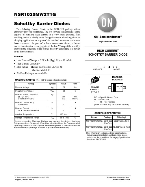
© Semiconductor Components Industries, LLC, 2006 August, 2006 − Rev. 0Publication Order Number:NSR1020MW2T1/DNSR1020MW2T1GSchottky Barrier DiodesThis Schottky Barrier Diode in the SOD−323 package offers extremely low Vf performance. The low forward voltage makes them capable of handling high current in a very small package. The resulting device is ideally suited for application as a blocking diode in charging applications or as part of discrete buck converter or discrete boost converter. As part of a buck conversion circuit, a boostconversion circuit or a charging circuit the low Vf drop of the schottky improves the efficiency of the overall device by consuming less power in the forward mode.Features•Low Forward V oltage − 0.24 V olts (Typ) @ I F = 10 mAdc •High Current Capability•ESD Rating− Human Body Model: CLASS 3B− Machine Model: C•Pb−Free Packages are AvailableMAXIMUM RATINGS(T J = 125°C unless otherwise noted)Rating Symbol Value Unit Reverse Voltage V R20Vdc Peak Revese Voltage VRM30V Forward Power Dissipation@ T A= 25°C Derate above 25°C P F2002.0mWmW/°CForward Current (DC) Continuous IF1AForward Currentt = 8.3 ms Half Sinewave I F5AJunction Temperature T J125 Max°C Storage Temperature Range T stg−55 to +150°C Stresses exceeding Maximum Ratings may damage the device. Maximum Ratings are stress ratings only. Functional operation above the Recommended Operating Conditions is not implied. Extended exposure to stresses above the Recommended Operating Conditions may affect device reliability.RE= Specific Device CodeM= Date CodeG= Pb−Free Package(Note: Microdot may be in either location)MARKINGDIAGRAMDevice Package Shipping†ORDERING INFORMATIONSOD−323CASE 477STYLE 1M†For information on tape and reel specifications, including part orientation and tape sizes, pleaserefer to our Tape and Reel Packaging Specification Brochure, BRD8011/D.NSR1020MW2T1G SOD−323(Pb−Free)3000/Tape & ReelNSR1020MW2T3G SOD−323(Pb−Free)10,000/Tape & Reel2ELECTRICAL CHARACTERISTICS (T A = 25°C unless otherwise noted)CharacteristicSymbol Min Typ Max Unit Total Capacitance (V R = 5.0 V, f = 1.0 MHz)C T −2529pF Reverse Leakage (V R = 15 V)I R −−40m Adc Forward Voltage (I F = 1 mAdc)V F −−0.20Vdc Forward Voltage (I F = 10 mAdc)V F −−0.26Vdc Forward Voltage (I F = 100 mAdc)V F−−0.33Vdc Forward Voltage (I F = 500 mAdc)V F −−0.44Vdc Forward Voltage (I F = 1000 mAdc)V F−−0.54Vdc1101001000I F , F O R W A R D C U R R E N T (m A )VR, REVERSE VOLTAGE (V)Figure 3. Total CapacitancePACKAGE DIMENSIONSSOD−323CASE 477−02ISSUE GSTYLE 1:PIN 1.CATHODE2.ANODE*For additional information on our Pb−Free strategy and solderingdetails, please download the ON Semiconductor Soldering and Mounting Techniques Reference Manual, SOLDERRM/D.SOLDERING FOOTPRINT*ǒmm inchesǓSCALE 10:1H E NOTES:1.DIMENSIONING AND TOLERANCING PER ANSI Y14.5M, 1982.2.CONTROLLING DIMENSION: MILLIMETERS.3.LEAD THICKNESS SPECIFIED PER L/F DRAWING WITH SOLDER PLATING.4.DIMENSIONS A AND B DO NOT INCLUDE MOLD FLASH, PROTRUSIONS OR GATE BURRS.5.DIMENSION L IS MEASURED FROM END OF RADIUS.NOTE 3DIM MIN NOM MAX MILLIMETERSA 0.800.90 1.00A10.000.050.10A30.15 REF b 0.250.320.4C 0.0890.120.177D 1.60 1.70 1.80E 1.15 1.25 1.350.082.30 2.50 2.70L 0.0310.0350.0400.0000.0020.0040.006 REF0.0100.0120.0160.0030.0050.0070.0620.0660.0700.0450.0490.0530.0030.0900.0980.105MIN NOM MAX INCHESON Semiconductor and are registered trademarks of Semiconductor Components Industries, LLC (SCILLC). SCILLC reserves the right to make changes without further notice to any products herein. SCILLC makes no warranty, representation or guarantee regarding the suitability of its products for any particular purpose, nor does SCILLC assume any liability arising out of the application or use of any product or circuit, and specifically disclaims any and all liability, including without limitation special, consequential or incidental damages.“Typical” parameters which may be provided in SCILLC data sheets and/or specifications can and do vary in different applications and actual performance may vary over time. All operating parameters, including “Typicals” must be validated for each customer application by customer’s technical experts. SCILLC does not convey any license under its patent rights nor the rights of others. SCILLC products are not designed, intended, or authorized for use as components in systems intended for surgical implant into the body, or other applications intended to support or sustain life, or for any other application in which the failure of the SCILLC product could create a situation where personal injury or death may occur. Should Buyer purchase or use SCILLC products for any such unintended or unauthorized application, Buyer shall indemnify and hold SCILLC and its officers, employees, subsidiaries, affiliates,and distributors harmless against all claims, costs, damages, and expenses, and reasonable attorney fees arising out of, directly or indirectly, any claim of personal injury or death associated with such unintended or unauthorized use, even if such claim alleges that SCILLC was negligent regarding the design or manufacture of the part. SCILLC is an Equal Opportunity/Affirmative Action Employer. This literature is subject to all applicable copyright laws and is not for resale in any manner.PUBLICATION ORDERING INFORMATION。
华汕电子 1020晶体管芯片说明书

PNP S I L I C O N T R A N S I S T O R
1020 晶体管芯片说明书
█ 芯片简介
█ 管芯示意图
芯片尺寸:4 英寸(100mm)
芯片代码:A075AJ-00
芯片厚度:240±20µm
管芯尺寸:750×750µm 2
焊位尺寸:B 极 165×170µm2;E 极 150×165µm2
集电极— 发射极饱和电压 基极— 发射极饱和电压 特征频率 共基极输出电容
最小值 典型值 最大值 单位
测试条件
-50
V IC=-100µA ,IE=0
-50
V IC=-10mA,IB=0
-5
V IE=-100µA ,IC=0
-1
µA VCB=-50V,IE=0
-1
µA VEB=-5V,IC=0
70
240
█ 电参数(Ta=25℃)CEO BVEBO ICBO IEBO hFE
VCE(sat) VBE(sat) fT Cob
符号说明 集电极— 基极击穿电压 集电极— 发射极击穿电压 发射极— 基极击穿电压 集电极— 基极截止电流 发射极— 基极截止电流 直流电流增益
电极金属:铝
背面金属:金
典型封装:2SA1020
█ 极限值(Ta=25℃)(TO-92L)
Tstg——贮存温度………………………………… -55~150℃ Tj——结温…………………………………………… 150℃ PC——集电极功率耗散( Ta=25℃)…………………900mW VCBO——集电极—基极电压……………………………-50V VCEO——集电极—发射极电压…………… ……………- 50 V VEBO —— 发射极— 基极电压…………………… ………-5 V IC——集电极电流………………………………………-2A IB——基极电流…………………………………………-0.5A
IR公司_大功率MOS管选型

I DContinuous Drain Current(A)70°Micro3Surface Mount PackagesV (BR)DSSDrain-to-Source Breakdown Voltage (V)R DS(on)On-State Resistance ()ΩI D Continuous Drain Current 25°C(A)R ΘMax.Thermal Resistance (°C/W)1FaxonDemand Number Case Outline KeyPartNumberPD Max.PowerDissipation (W)N-ChannelLogic LevelIRLML2402*912570.54200.25 1.20.95230H1IRLML2803912580.54300.251.20.93230P-ChannelLogic LevelIRLML6302*912590.54-200.6-0.62-4.8230H1IRLML5103912600.54-300.6-0.61-4.8230* Indicates low VGS(th), which can operate at VGS = 2.7VMeasured at ambient for Micro3, Micro6, Micro8, SO-8, and SOT-223 package styles. All others measured at case.1Micro3SO-8D-PakD -PakSOT-227Micro6SOT-223Micro82 Illustrations not to scaleI DContinuous Drain Current(A)70°Micro6Surface Mount PackagesV (BR)DSSDrain-to-Source Breakdown Voltage (V)R DS(on)On-State Resistance ()ΩI D Continuous Drain Current 25°C(A)R ΘMax.Thermal Resistance (°C/W)1FaxonDemand Number Case Outline KeyPartNumberPD Max.PowerDissipation (W)N-ChannelLogic LevelIRLMS1902915401.7200.10 3.2 2.675H2IRLMS1503915081.7300.103.22.675P-ChannelLogic LevelIRLMS6702*914141.7-200.20-2.3-1.975H2IRLMS5703914131.7-300.20-2.3-1.975* Indicates low VGS(th), which can operate at VGS = 2.7VMeasured at ambient for Micro3, Micro6, Micro8, SO-8, and SOT-223 package styles. All others measured at case.1Micro3SO-8D-PakD -PakSOT-227Micro6SOT-223Micro82 Illustrations not to scaleI DContinuous Drain Current(A)70°Micro8Surface Mount PackagesV (BR)DSSDrain-to-Source Breakdown Voltage (V)R DS(on)On-State Resistance ()ΩI D Continuous Drain Current 25°C(A)R ΘMax.Thermal Resistance (°C/W)1FaxonDemand Number Case Outline KeyPart NumberP D Max.PowerDissipation (W)N-Channel Logic LevelIRF7601* 912611.820 0.035 5.7 4.6 70 H3IRF7603 912621.830 0.035 5.6 4.5 70Dual N-Channel Logic LevelIRF7501* 912651.220 0.135 2.4 1.9 100 H3IRF7503 912661.2530 0.135 2.4 1.9 100P-Channel Logic LevelIRF7604* 912631.8-20 0.09 -3.6 -2.9 70 H3IRF7606 912641.8-30 0.09 -3.6 -2.9 70Dual P-Channel Logic LevelIRF7504* 912671.25-20 0.27 -1.7 -1.4 100 H3IRF7506 912681.25-30 0.27 -1.7 -1.4 100Dual N- and P-Channel Logic LevelIRF7507* 912691.2520 0.1352.4 1.9 100 H3-20 0.27 -1.7 -1.4IRF7509 912701.2530 0.135 2.4 1.9 100-30 0.27 -1.7 -1.4* Indicates low VGS(th), which can operate at VGS = 2.7VMeasured at ambient for Micro3, Micro6, Micro8, SO-8, and SOT-223 package styles. All others measured at case.1Micro3SO-8D-Pak D -PakSOT-227Micro6SOT-223Micro8 2 Illustrations not to scaleI DContinuous Drain Current(A)70°SO-8Surface Mount PackagesV (BR)DSSDrain-to-Source Breakdown Voltage (V)R DS(on)On-State Resistance ()ΩI D Continuous Drain Current 25°C(A)R ΘMax.Thermal Resistance (°C/W)1FaxonDemand Number Case Outline KeyPart Number P D Max.PowerDissipation (W)N-ChannelIRF7413913302.5300.011139.250H4IRF7413A 916132.5300.0135128.450IRF9410915622.5300.0375.850Dual N-ChannelIRF7311914352.0200.029 6.6 5.362.5H4IRF7313914802.0300.029 6.5 5.262.5IRF7333917002.0300.10 3.5 2.862.5917002.0300.050 4.9 3.962.5IRF9956915592.0300.103.52.862.5Dual P-ChannelIRF7314914352.0-200.058-5.3-4.362.5H4IRF7316915052.0-300.058-4.9-3.962.5IRF9953915602.0-300.25-2.3-1.862.5* Indicates low VGS(th), which can operate at VGS = 2.7VMeasured at ambient for Micro3, Micro6, Micro8, SO-8, and SOT-223 package styles. All others measured at case.1Micro3SO-8D-PakD -PakSOT-227Micro6SOT-223Micro82 Illustrations not to scaleI DContinuous Drain Current(A)70°SO-8Surface Mount PackagesV (BR)DSSDrain-to-Source Breakdown Voltage (V)R DS(on)On-State Resistance ()ΩI D Continuous Drain Current 25°C(A)RΘMax.ThermalResistance(°C/W)1FaxonDemand Number Case Outline KeyPart NumberP D Max.PowerDissipation (W)Dual N- and P-ChannelIRF7317 915682.020 0.029 6.6 5.3 62.5 H42.0-20 0.058 -5.3 -4.3 62.5IRF9952 915622.030 0.103.5 2.8 62.5915622.0-30 0.25 -2.3 -1.8 62.5IRF7319 916062.030 0.029 6.5 5.2 62.52.0-30 0.058 -4.9 -3.9 62.5* Indicates low VGS(th), which can operate at VGS = 2.7VMeasured at ambient for Micro3, Micro6, Micro8, SO-8, and SOT-223 package styles. All others measured at case.1Micro3SO-8D-Pak D -PakSOT-227Micro6SOT-223Micro8 2 Illustrations not to scaleI DContinuous Drain Current(A)70°SO-8Surface Mount PackagesV (BR)DSSDrain-to-Source Breakdown Voltage (V)R DS(on)On-State Resistance ()ΩI D Continuous Drain Current 25°C(A)R ΘMax.Thermal Resistance (°C/W)1FaxonDemand Number Case Outline KeyPart Number P D Max.PowerDissipation (W)N-ChannelLogic LevelIRF7401912442.5200.0228.77.050H4IRF7201911002.5300.0307.0 5.650IRF7403912452.5300.0228.55.450Dual N-ChannelLogic LevelIRF7101908712.0200.10 3.5 2.362.5H4IRF7301912382.0200.050 5.2 4.162.5IRF7303912392.0300.050 4.9 3.962.5IRF7103910952.0500.1303.02.362.5P-ChannelLogic LevelIRF7204911032.5-200.060-5.3-4.250H4IRF7404912462.5-200.040-6.7-5.450IRF7205911042.5-300.070-4.6-3.750IRF7406912472.5-300.045-5.8-3.750IRF7416913562.5-300.02-10-7.150* Indicates low VGS(th), which can operate at VGS = 2.7VMeasured at ambient for Micro3, Micro6, Micro8, SO-8, and SOT-223 package styles. All others measured at case.1Micro3SO-8D-PakD -PakSOT-227Micro6SOT-223Micro82 Illustrations not to scaleI DContinuous Drain Current(A)70°SO-8Surface Mount PackagesV (BR)DSSDrain-to-Source Breakdown Voltage (V)R DS(on)On-State Resistance ()ΩI D Continuous Drain Current 25°C(A)R ΘMax.Thermal Resistance (°C/W)1FaxonDemand Number Case Outline KeyPart Number P D Max.PowerDissipation (W)Dual P-ChannelLogic LevelIRF7104910962.0-200.250-2.3-1.862.5H4IRF7304912402.0-200.090-4.3-3.462.5IRF7306912412.0-300.10-3.6-2.962.5Dual N- and P-Channe Logic LevelIRF7307912421.4200.050 4.3 3.490H4-200.090-3.6-2.9IRF7105910972.0250.1093.5 2.862.52-250.25-2.3-1.862IRF7309912432.0300.050 4.9 3.962.5-300.10-3.6-2.9* Indicates low VGS(th), which can operate at VGS = 2.7VMeasured at ambient for Micro3, Micro6, Micro8, SO-8, and SOT-223 package styles. All others measured at case.1Micro3SO-8D-PakD -PakSOT-227Micro6SOT-223Micro82 Illustrations not to scaleI DContinuous Drain Current(A)70°SOT-223Surface Mount PackagesV (BR)DSSDrain-to-Source Breakdown Voltage (V)R DS(on)On-State Resistance ()ΩI D Continuous Drain Current 25°C(A)R ΘMax.Thermal Resistance (°C/W)1FaxonDemand Number Case Outline KeyPart Number P D Max.PowerDissipation (W)N-ChannelIRFL4105913812.1550.045 3.7 3.060H6IRFL110908612.01000.54 1.50.9660IRFL4310913682.11000.20 1.6 1.360IRFL21090868 2.02001.50.960.660IRFL214908622.02502.00.790.560P-ChannelIRFL9110908642.0-1001.2-1.1-0.6960H6N-ChannelLogic LevelIRLL3303913792.1300.031 4.6 3.760H6IRLL014N 914992.1550.14 2.0 1.660IRLL2705913802.1550.043.83.060* Indicates low VGS(th), which can operate at VGS = 2.7VMeasured at ambient for Micro3, Micro6, Micro8, SO-8, and SOT-223 package styles. All others measured at case.1Micro3SO-8D-PakD -PakSOT-227Micro6SOT-223Micro82 Illustrations not to scaleI DContinuous Drain Current(A)100°D-PakSurface Mount PackagesV (BR)DSSDrain-to-Source Breakdown Voltage (V)R DS(on)On-State Resistance ()ΩI D Continuous Drain Current 25°C(A)R ΘMax.Thermal Resistance (°C/W)1FaxonDemand Number Case Outline KeyPart Number P D Max.PowerDissipation (W)N-ChannelIRFR33039164257300.0313321 2.2H7IRFR024N9133638550.0751610 3.3IRFR41059130248550.0452516 2.7IRFR12059131869550.0273723 1.8IRFR11090524251000.54 4.3 2.75IRFR120N 91365391000.219.1 5.8 3.2IRFR391091364521000.11159.5 2.4IRFR2109052625200 1.5 2.6 1.75IRFR22090525422000.8 4.833IRFR21490703252502 2.2 1.45IRFR2249060042250 1.1 3.8 2.43IRFR3109059725400 3.6 1.7 1.15IRFR3209059842400 1.8 3.123IRFR42090599425003 2.4 1.53IRFRC2090637426004.421.33* Indicates low VGS(th), which can operate at VGS = 2.7VMeasured at ambient for Micro3, Micro6, Micro8, SO-8, and SOT-223 package styles. All others measured at case.1Micro3SO-8D-PakD -PakSOT-227Micro6SOT-223Micro82 Illustrations not to scaleI DContinuous Drain Current(A)100°D-PakSurface Mount PackagesV (BR)DSSDrain-to-Source Breakdown Voltage (V)R DS(on)On-State Resistance ()ΩI D Continuous Drain Current 25°C(A)R ΘMax.Thermal Resistance (°C/W)1FaxonDemand Number Case Outline KeyPart Number P D Max.PowerDissipation (W)P-ChannelIRFR55059161057-550.11-18-11 2.2H7IRFR53059140289-550.065-28-18 1.4IRFR90149065425-600.5-5.1-3.25IRFR90249065542-600.28-8.8-5.63IRFR91109051925-100 1.2-3.1-25IRFR91209052042-1000.6-5.6-3.63IRFR9120N 9150739-1000.48-6.5-4.1 3.2IRFR92109052125-2003-1.9-1.25IRFR92209052242-200 1.5-3.6-2.33IRFR92149165850-250 3.0-2.7-1.7 2.5IRFR93109166350-4007.0-1.8-1.12.5* Indicates low VGS(th), which can operate at VGS = 2.7VMeasured at ambient for Micro3, Micro6, Micro8, SO-8, and SOT-223 package styles. All others measured at case.1Micro3SO-8D-PakD -PakSOT-227Micro6SOT-223Micro82 Illustrations not to scaleI DContinuous Drain Current(A)100°D-PakSurface Mount PackagesV (BR)DSSDrain-to-Source Breakdown Voltage (V)R DS(on)On-State Resistance ()ΩI D Continuous Drain Current 25°C(A)R ΘMax.Thermal Resistance (°C/W)1FaxonDemand Number Case Outline KeyPart Number P D Max.PowerDissipation (W)N-ChannelLogic LevelIRLR27039133538300.0452214 3.3H7IRLR33039131657300.0313321 2.2IRLR31039133369300.0194629 1.8IRLR024N 9136338550.0651711 3.3IRLR27059131746550.042415 2.7IRLR29059133469550.0273623 1.8IRLR120N 91541391000.18511 6.9 3.2IRLR341091607521000.10159.52.4* Indicates low VGS(th), which can operate at VGS = 2.7VMeasured at ambient for Micro3, Micro6, Micro8, SO-8, and SOT-223 package styles. All others measured at case.1Micro3SO-8D-PakD -PakSOT-227Micro6SOT-223Micro82 Illustrations not to scaleI DContinuous Drain Current(A)100°D 2PakSurface Mount PackagesV (BR)DSSDrain-to-Source Breakdown Voltage (V)R DS(on)On-State Resistance ()ΩI D Continuous Drain Current 25°C(A)R ΘMax.Thermal Resistance (°C/W)1FaxonDemand Number Case Outline KeyPart NumberP D Max.PowerDissipation (W)N-ChannelIRFZ24NS 913554555 0.07 17 12 3.3 H10IRFZ34NS 913116855 0.04 29 20 2.2IRFZ44NS 9131511055 0.022 49 35 1.4IRFZ46NS 9130512055 0.020 53 37 1.3IRFZ48NS 9140814055 0.016 64 45 1.1IRF1010NS 913723.855 0.011 84 60 40IRF3205S 9130420055 0.008 110 80 0.75IRFZ44ES 9171411060 0.023 48 34 1.4IRF1010ES 9172017060 0.012 83 59 0.90IRF2807S 9151815075 0.013 71 50 1.0IRF520NS 9134047100 0.2 9.5 6.7 3.2IRF530NS 9135263100 0.11 15 11 2.4IRF540NS 91342110100 0.052 27 19 1.6IRF1310NS 91514120100 0.036 36 25 1.3IRF3710S 91310150100 0.028 46 33 1.0IRF3315S 9161794150 0.082 21 15 1.6IRF3415S 91509150150 0.042 37 26 1.0IRFBC20S 9.101450600 4.4 2.2 1.4 2.5IRFBC30S 9101574600 2.2 3.6 2.3 1.7IRFBC40S 91016130600 1.2 6.2 3.9 1.0* Indicates low VGS(th), which can operate at VGS = 2.7VMeasured at ambient for Micro3, Micro6, Micro8, SO-8, and SOT-223 package styles. All others measured at case.1Micro3SO-8D-Pak D -PakSOT-227Micro6SOT-223Micro8 2 Illustrations not to scaleI DContinuous Drain Current(A)100°D 2PakSurface Mount PackagesV (BR)DSSDrain-to-Source Breakdown Voltage (V)R DS(on)On-State Resistance ()ΩI D Continuous Drain Current 25°C(A)R ΘMax.Thermal Resistance (°C/W)1FaxonDemandNumberCase Outline KeyPart NumberP D Max.PowerDissipation (W)IRFBF20S 9166554900 8.0 1.7 1.1 2.3 H10P-ChannelIRF5305S 91386110-55 0.06 -31 -22 1.4 H10IRF4905S 914783.8-55 0.02 -74 -52 40IRF9520NS 9152247-100 0.48 -6.7 -4.8 3.2IRF9530NS 9152375-100 0.20 -14 -9.9 2.0IRF9540NS 9148394-100 0.117 -19 -13 1.6IRF5210S 91405150-100 0.06 -35 -25 1.0* Indicates low VGS(th), which can operate at VGS = 2.7VMeasured at ambient for Micro3, Micro6, Micro8, SO-8, and SOT-223 package styles. All others measured at case.1Micro3SO-8D-Pak D -PakSOT-227Micro6SOT-223Micro8 2 Illustrations not to scaleI DContinuous Drain Current(A)100°D 2PakSurface Mount PackagesV (BR)DSSDrain-to-Source Breakdown Voltage (V)R DS(on)On-State Resistance ()ΩI D Continuous Drain Current 25°C(A)R ΘMax.Thermal Resistance (°C/W)1FaxonDemand Number Case Outline KeyPart NumberP D Max.PowerDissipation (W)N-Channel Logic LevelIRL3302S 916925720 0.020 39 25 2.2 H10IRL3202S916756920 0.016 48 30 1.8IRL3102S 916918920 0.013 61 39 1.4IRL3402S 9169311020 0.01 85 54 1.1IRL3502S 9167614020 0.007 110 67 0.89IRL2703S 913604530 0.04 24 17 3.3IRL3303S 913236830 0.026 38 27 2.2IRL3103S 9133811030 0.014 64 45 1.4IRL2203NS 9136717030 0.007 116 82 0.90IRL3803S 9131920030 0.006 140 98 0.75IRLZ24NS 913584555 0.06 18 13 3.3IRLZ34NS 913086855 0.035 30 21 2.2IRLZ44NS 9134711055 0.022 47 33 1.4IRL3705NS 9150217055 0.01 89 63 0.90IRL2505S 9132620055 0.008 104 74 0.75IRLZ44S 9090615060 0.028 50 36 1.0IRL530NS 9134963100 0.1 15 11 2.4IRL2910S 91376150100 0.026 48 34 1.0* Indicates low VGS(th), which can operate at VGS = 2.7VMeasured at ambient for Micro3, Micro6, Micro8, SO-8, and SOT-223 package styles. All others measured at case.1Micro3SO-8D-Pak D -PakSOT-227Micro6SOT-223Micro8 2 Illustrations not to scaleI DContinuous Drain Current(A)100°SOT-227Surface Mount PackagesV (BR)DSSDrain-to-Source Breakdown Voltage (V)R DS(on)On-State Resistance ()ΩI D Continuous DrainCurrent 25°C(A)RΘMax.Thermal Resistance (°C/W)1FaxonDemand Number Case Outline KeyPart Number P D Max.PowerDissipation (W)N-ChannelFully Isolated Low ChargeFA38SA50LC 916155005000.1338240.25H21FA57SA50LC916506255000.0857360.20* Indicates low VGS(th), which can operate at VGS = 2.7VMeasured at ambient for Micro3, Micro6, Micro8, SO-8, and SOT-223 package styles. All others measured at case.1Micro3SO-8D-PakD -PakSOT-227Micro6SOT-223Micro82 Illustrations not to scaleI DContinuous Drain Current(A)100°I-PakThrough-Hole PackagesV (BR)DSSDrain-to-Source Breakdown Voltage (V)R DS(on)On-State Resistance ()ΩI D Continuous Drain Current 25°C(A)R ΘMax.Thermal Resistance (°C/W)1FaxonDemand Number Case Outline KeyPart Number P D Max.PowerDissipation (W)N-ChannelIRFU33039164257300.0313321 2.2H8IRFU024N 9133638550.0751610 3.3IRFU41059130248550.0452519 2.7IRFU12059131869550.0273723 1.8IRFU11090524251000.54 4.3 2.7 5.0IRFU120N 91365391000.219.1 5.8 3.2IRFU391091364521000.11159.5 2.4IRFU2109052625200 1.5 2.6 1.7 5.0IRFU22090525422000.80 4.8 3.0 3.0IRFU2149070325250 2.0 2.2 1.4 5.0IRFU2249060042250 1.1 3.8 2.4 3.0IRFU3109059725400 3.6 1.7 1.1 5.0IRFU3209059842400 1.8 3.1 2.0 3.0IRFU4209059942500 3.0 2.4 1.5 3.0IRFUC2090637426004.42.01.33.0I-PakTO-220 FullPakTO-262TO-247HEXDIPTO-220AB Illustrations not to scale** Not ratedI DContinuous Drain Current(A)100°I-PakThrough-Hole PackagesV (BR)DSSDrain-to-Source Breakdown Voltage (V)R DS(on)On-State Resistance ()ΩI D Continuous Drain Current 25°C(A)R ΘMax.Thermal Resistance (°C/W)1FaxonDemand Number Case Outline KeyPart Number P D Max.PowerDissipation (W)P-ChannelIRFU55059161057-550.11-18-11 2.2H8IRFU53059140289-550.065-28-18 1.4IRFU90149065425-600.50-5.1-3.2 5.0IRFU90249065542-600.28-8.8-5.6 3.0IRFU91109051925-100 1.2-3.1-2.0 5.0IRFU91209052042-1000.60-5.6-3.6 3.0IRFU9120N 9150739-1000.48-6.5-4.1 3.2IRFU92109052125-200 3.0-1.9-1.2 5.0IRFU92209052242-200 1.5-3.6-2.3 3.0IRFU92149165850-2503.0-2.7-1.7 2.5IRFU93109166350-4007.0-1.8-1.12.5N-ChannelLogic LevelIRLU27039133538300.0452214 3.3H8IRLU33039131657300.0313321 2.2IRLU31039133369300.0194629 1.8IRLU024N 9136338550.0651711 3.3IRLU27059131746550.04241715IRLU29059133469550.0273623 1.8IRLU120N 91541391000.18511 6.9 3.2IRLU341091607521000.10159.52.4I-PakTO-220 FullPakTO-262TO-247HEXDIPTO-220AB Illustrations not to scale** Not ratedI DContinuous Drain Current(A)100°HEXDIPThrough-Hole PackagesV (BR)DSSDrain-to-Source Breakdown Voltage (V)R DS(on)On-State Resistance ()ΩI D Continuous Drain Current 25°C(A)R ΘMax.Thermal Resistance (°C/W)1FaxonDemand Number Case Outline KeyPart Number P D Max.PowerDissipation (W)N-ChannelIRFD014907001.3600.2 1.7 1.2120H9IRFD024906991.3600.1 2.5 1.8120IRFD110903281.31000.54 1.00.71120IRFD120903851.31000.27 1.30.94120IRFD210903861.3200 1.50.60.38120IRFD220904171.32000.80.80.50120IRFD214912711.3250 2.00.570.32120IRFD224912721.3250 1.10.760.43120IRFD310912251.3400 3.60.420.23120IRFD320912261.3400 1.80.600.33120IRFD420912271.3500 3.00.460.26120IRFDC20912281.36004.40.320.21120I-PakTO-220 FullPakTO-262TO-247HEXDIPTO-220AB Illustrations not to scale** Not ratedI D Continuous Drain Current (A)100°TO-220Qg TotalGate Charge(nC)Through-Hole PackagesV (BR)DSSDrain-to-Source Breakdown Voltage (V)R DS(on)On-State Resistance ()ΩI D Continuous Drain Current 25°C (A)R ΘMax.Thermal Resistance(°C/W)1Faxon Demand Number Case OutlineKeyPart Number P D Max.Power Dissipation (W)N-ChannelLow ChargeIRF737LC91314743000.75 6.1** 1.7 3.9H11IRF740LC 910681254000.5510** 1.039IRF840LC 910691255000.858.0** 1.039IRFBC40LC910701256001.26.2**1.039I-PakTO-220 FullPakTO-262TO-247HEXDIPTO-220AB Illustrations not to scale** Not ratedI DContinuous Drain Current(A)100°TO-220ABThrough-Hole PackagesV (BR)DSSDrain-to-Source Breakdown Voltage (V)R DS(on)On-State Resistance ()ΩI D Continuous Drain Current 25°C(A)R ΘMax.Thermal Resistance (°C/W)1FaxonDemand Number Case Outline KeyPart Number P D Max.PowerDissipation (W)N-ChannelIRFZ24N 9135445550.071712 3.3H12IRFZ34N9127656550.042618 2.7IRFZ44N 9130383550.0244129 1.8IRFZ46N 9127788550.024633 1.7IRFZ48N 9140694550.0165337 1.6IRF1010N 91278130550.0127251 1.2IRF320591279150550.0089869 1.0IRFZ34E 9167268600.0422820 2.2IRFZ44E 91671110600.0234834 1.4IRF1010E 91670170600.01281570.90IRF280791517150750.0137150 1.0IRF520N 91339471000.209.5 6.79.5IRF530N 91351601000.111511 2.4IRF540N 91341941000.0522719 1.6IRF1310N 916111201000.0363625 1.3IRF3710913091501000.0284633 1.0IRF331591623941500.0822115 1.6IRF3415914771501500.0423726 1.0IRFBC209062350600 4.4 2.2 1.4 2.5IRFBC309048274600 2.2 3.6 2.3 1.7IRFBC4090506125600 1.2 6.2 3.9 1.0IRFBE2090610548006.51.81.22.3I-PakTO-220 FullPakTO-262TO-247HEXDIPTO-220AB Illustrations not to scale** Not ratedI DContinuous Drain Current(A)100°TO-220ABThrough-Hole PackagesV (BR)DSSDrain-to-Source Breakdown Voltage (V)R DS(on)On-State Resistance ()ΩI D Continuous Drain Current 25°C(A)R ΘMax.Thermal Resistance (°C/W)1FaxonDemand Number Case Outline KeyPart Number P D Max.PowerDissipation (W)IRFBE3090613125800 3.0 4.1 2.6 2.0H12IRFBF3090616125900 3.7 3.6 2.3 1.0IRFBG209060454100011 1.40.86 2.3IRFBG309062012510005.03.12.01.0P-ChannelIRF9Z24N 9148445-550.175-12-8.53.3H12IRF9Z34N 9148556-550.10-17-12 2.7IRF530591385110-550.06-31-22 1.4IRF490591280150-550.02-64-45 1.0IRF9530N 9148275-1000.20-13-9.2 2.0IRF9540N 9143794-1000.117-19-13 1.6IRF521091434150-1000.06-35-25 1.0IRF62159147983-1500.29-11-7.81.8I-PakTO-220 FullPakTO-262TO-247HEXDIPTO-220AB Illustrations not to scale** Not ratedI DContinuous Drain Current(A)100°TO-220ABThrough-Hole PackagesV (BR)DSSDrain-to-Source Breakdown Voltage (V)R DS(on)On-State Resistance ()ΩI D Continuous Drain Current 25°C(A)R ΘMax.Thermal Resistance (°C/W)1FaxonDemand Number Case Outline KeyPart NumberP D Max.PowerDissipation (W)N-Channel Logic LevelIRL3302 916965720 0.020 39 25 2.2 H12IRL3202 916956920 0.016 48 30 1.8IRL3102 916948920 0.013 61 39 1.4IRL3402 9169711020 0.01 85 54 1.1IRL3502 9169814020 0.007 110 67 0.89IRL2703 913594530 0.04 24 17 3.3IRL3303 913225630 0.026 34 24 2.7IRL3103 913378330 0.014 56 40 1.8IRL2203N 9136613030 0.007 100 71 1.230 0.007 61 43 3.2IRL3803 9130115030 0.006 120 83 1.0IRLZ24N 913574555 0.06 18 13 3.3IRLZ34N 913075655 0.035 27 19 2.7IRLZ44N 913468355 0.022 41 29 1.8IRL3705N 9137013055 0.01 77 54 1.2IRL2505 9132520055 0.008 104 74 0.75IRL520N 9149447100 0.18 10 7.1 3.2IRL530N 9134863100 0.10 15 11 2.4IRL540N 9149594100 0.044 30 21 1.6IRL2910 91375150100 0.026 48 34 1.0I-PakTO-220 FullPakTO-262TO-247HEXDIPTO-220AB Illustrations not to scale** Not ratedI D Continuous Drain Current (A)100°TO-220 FullPak (Fully Isolated)Qg TotalGate Charge(nC)Through-Hole PackagesV (BR)DSSDrain-to-Source Breakdown Voltage (V)R DS(on)On-State Resistance ()ΩI D Continuous DrainCurrent 25°C(A)R ΘMax.Thermal Resistance (°C/W)1Fax on Demand Number Case OutlineKeyPart Number P D Max.Power Dissipation (W)N-ChannelLow ChargeIRFI740GLC91209404000.55 6.0** 3.139H13IRFI840GLC 91208405000.85 4.8** 3.139IRFIBC40GLC91211406001.24.0**3.139I-PakTO-220 FullPakTO-262TO-247HEXDIPTO-220AB Illustrations not to scale** Not ratedI DContinuous Drain Current(A)100°TO-220 FullPak (Fully Isolated)Through-Hole PackagesV (BR)DSSDrain-to-Source Breakdown Voltage (V)R DS(on)On-State Resistance ()ΩI D Continuous Drain Current 25°C(A)R ΘMax.Thermal Resistance (°C/W)1FaxonDemand Number Case Outline KeyPart Number P D Max.PowerDissipation (W)N-ChannelIRFIZ24N 9150126550.07139.2 5.8H14IRFIZ34N9148931550.041913 4.8IRFIZ44N 9140338550.02428200.024IRFIZ46N 9130640550.023122 3.8IRFIZ48N 9140742550.0163625 3.6IRFI1010N 9137347550.0124431 3.2IRFI32059137448550.0085640 3.1IRFIZ24E 9167329600.071149.6 5.2IRFIZ34E 9167437600.0422115 4.1IRFI510G 90829271000.54 4.5 3.2 5.5IRFI520N 91362271000.207.2 5.1 5.5IRFI530N 91353331000.11117.8 4.5IRFI540N 91361421000.0521813 3.6IRFI1310N 91611451000.0362216 3.3IRFI371091387481000.0252820 3.1IRFI620G 90832302000.8 4.1 2.6 4.1IRFI630G 90652322000.4 5.9 3.7 3.6IRFI640G 90649402000.189.8 6.2 3.1IRFI614G 9083123250 2.0 2.1 1.3 5.5IRFI624G 9083330250 1.1 3.4 2.2 4.1IRFI634G 90738322500.45 5.6 3.5 3.6IRFI644G 90739402500.287.953.1I-PakTO-220 FullPakTO-262TO-247HEXDIPTO-220AB Illustrations not to scale** Not ratedI DContinuous Drain Current(A)100°TO-220 FullPak (Fully Isolated)Through-Hole PackagesV (BR)DSSDrain-to-Source Breakdown Voltage (V)R DS(on)On-State Resistance ()ΩI D Continuous Drain Current 25°C(A)R ΘMax.Thermal Resistance (°C/W)1FaxonDemand Number Case Outline KeyPart Number P D Max.PowerDissipation (W)IRFI720G 9083430400 1.8 2.6 1.7 4.1H14IRFI730G 9065032400 1.0 3.7 2.3 3.6IRFI740G 90651404000.55 5.4 3.4 3.1IRFI734G 9100135450 1.2 3.4 2.1 3.6IRFI744G 91002404500.63 4.9 3.1 3.1IRFI820G 9064130500 3.0 2.1 1.3 4.1IRFI830G 9064632500 1.5 3.12 3.6IRFI840G 90642405000.85 4.6 2.9 3.1IRFIBC20G 90850306004.41.71.1 4.1IRFIBC30G 90851356002.2 2.5 1.63.6IRFIBC40G 9085240600 1.2 3.5 2.2 3.1IRFIBE20G 9085330800 6.5 1.4.86 4.1IRFIBE30G 9085435800 3.0 2.1 1.4 3.6IRFIBF20G 90855309008.0 1.2.79 4.1IRFIBF30G90856359003.71.91.23.6P-ChannelIRFI9Z24N 9152929-550.175-9.5-6.7 5.2H14IRFI9Z34N 9153037-550.10-14-10 4.1IRFI49059152663-550.02-41-29 2.4IRFI9540G 9083742-1000.117-13-9.2 3.6IRFI9540N 9148742-1000.117-13-9.2 3.6IRFI52109140448-1000.06-20-14 3.1IRFI9634G 9148835-2501.0-4.1-2.63.6I-PakTO-220 FullPakTO-262TO-247HEXDIPTO-220AB Illustrations not to scale** Not ratedI DContinuous Drain Current(A)100°TO-220 FullPak (Fully Isolated)Through-Hole PackagesV (BR)DSSDrain-to-Source Breakdown Voltage (V)R DS(on)On-State Resistance ()ΩI D Continuous Drain Current 25°C(A)R ΘMax.Thermal Resistance (°C/W)1FaxonDemand Number Case Outline KeyPart Number P D Max.PowerDissipation (W)N-ChannelLogic LevelIRLI2203N 9137847300.0076143 3.2H14IRLI38039132048300.0066747 3.1IRLIZ24N 9134426550.06149.9 5.8IRLIZ34N 9132931550.0352014 4.8IRLIZ44N 9149838550.0222820 4.0IRLI3705N 9136947550.014733 3.2IRLI25059132763550.00858412.4IRLI520N 91496271000.187.7 5.4 5.5IRLI530N 91350331000.10117.8 4.5IRLI540N 91497421000.04420143.6IRLI291091384481000.02627193.1P-ChannelLogic LevelIRFI9520G 9083537-1000.6-5.2-3.6 4.1H14IRFI9530G 9083638-1000.03-7.7-5.4 3.6IRFI9620G 9087430-200 1.5-3.0-1.9 4.1IRFI9630G 9083840-2000.8-4.3-2.7 3.6IRFI9640G9083940-2000.5-6.1-3.93.1I-PakTO-220 FullPakTO-262TO-247HEXDIPTO-220AB Illustrations not to scale** Not ratedI D Continuous Drain Current (A)100°TO-247Qg TotalGate Charge(nC)Through-Hole PackagesV (BR)DSSDrain-to-Source Breakdown Voltage (V)R DS(on)On-State Resistance ()ΩI D Continuous Drain Current 25°C (A)R ΘMax.Thermal Resistance (°C/W)1Fax on Demand Number Case OutlineKeyPart Number P D Max.Power Dissipation (W)1N-ChannelLow ChargeIRFP350LC912291904000.3018**0.6570H16IRFP360LC 912302804000.2023**0.4598IRFP450LC 912311905000.4016**0.6570IRFP460LC 912322805000.2720**0.4598IRFPC50LC 912331906000.6013**0.6570IRFPC60LC912342806000.4016**0.4598I-PakTO-220 FullPakTO-262TO-247HEXDIPTO-220AB Illustrations not to scale** Not rated。
伯克尼斯4.203.2直流柴油发动机的零件说明书
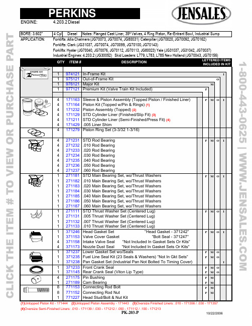
(4)Oversize Semi-Finished Liners: .010 - 171139 / .030 - 171212 / .050 - 171112 / .100 - 171213PK-203-P 10/22/2006APPLICATION: Forklifts: Allis Chalmers (JG70073, JG70074, JG80031) Caterpillar (JG70020, JG70092, JG70162)Forklifts: Clark (JG31037, JG70074, JG70099, JG70100, J G70143)Forklifts: Hyster (JG70040, JG70076, JG70112, JG70113, JG80023) Yale (JG31037, JG31042, JG70037)Industrial Engines: 4.203.2 (JG30052) Skid Loaders: L779, L783, L785 New Holland (JG70043, JG70156)QTY ITEM # DESCRIPTION LETTERED ITEMSINCLUDED IN KIT1 974121 In-Frame Kit I1 975121 Out-of-Frame Kit O1 976121 Major Kit M1 977121 Premium Kit (Valve Train Kit Included) P4 171163 Sleeve & Piston Assembly (Topped Piston / Finished Liner) P M O I4 171164 Piston Kit (Topped w/Pin & Rings) (1)4 171232 Piston Assembly (Topped) (2)4 171129 STD Cylinder Liner (Finished/Slip Fit) (3)4 171211 STD Cylinder Liner (Semi-Finished/Press Fit) (4)4 171429 .005 Liner Shim4 171279 Piston Ring Set (3-3/32 1-3/16)4 271231 STD Rod Bearing P M O I4 271232 .010 Rod Bearing4 271233 .020 Rod Bearing4 271234 .030 Rod Bearing4 271235 .040 Rod Bearing4 271236 .050 Rod Bearing4 271237 .060 Rod Bearing1 271181 STD Main Bearing Set, wo/Thrust Washers P M O I1 271182 .010 Main Bearing Set, wo/Thrust Washers1 271183 .020 Main Bearing Set, wo/Thrust Washers1 271184 .030 Main Bearing Set, wo/Thrust Washers1 271185 .040 Main Bearing Set, wo/Thrust Washers1 271186 .050 Main Bearing Set, wo/Thrust Washers1 271187 .060 Main Bearing Set, wo/Thrust Washers1 271111 STD Thrust Washer Set (Centered Lug) P M O I1 271131 .005 Thrust Washer Set (Centered Lug)1 271132 .007 Thrust Washer Set (Centered Lug)1 271133 .010 Thrust Washer Set (Centered Lug)1 371246 Head Gasket Set "Head Gasket - 371242" P M O I1 371153 Valve Cover Gasket "Bolt Seal - 371247" 4 371158 Intake Valve Seal "Not Included In Gasket Sets Or Kits"4 371173 Nozzle Dust Seal "Not Included In Gasket Sets Or Kits"1 1 1 371237 371235 371238 Lower Gasket Set wo/Seals Fuel Line Seal Kit (23 Seals & Washers) "Not In Gkt Sets" Pan Gasket Set (Industrial Pan Not Bolted To Timing Cover) P P M M O OI1 1 371233 371145 Front Crank Seal Rear Crank Seal (Viton Lip Type) P P M M O O4 271175 Pin Bushing P M1 271189 Cam Bearing P M8 771153 Connecting Rod Bolt P M 8 771152 Connecting Rod Nut P M1 771227 Head Stud/Bolt & Nut Kit(1)Untopped Piston Kit - 171444 (2)Untopped Piston Assembly - 171443 (3)Oversize Finished Liners: .010 - 171356 / .030 - 171357(5)Adjusting Screw Lock Nut - 571139(6)Rocker Arm Shaft Plug - 471176PK-203-P (7)Rocker Arm Shaft Snap Ring - 47117710/22/2006Forklifts: Clark (JG31037, JG70074, JG70099, JG70100, J G70143)Forklifts: Hyster (JG70040, JG70076, JG70112, JG70113, JG80023) Yale (JG31037, JG31042, JG70037)QTYITEM #DESCRIPTIONLETTERED ITEMSINCLUDED IN KIT1979511 Camshaft Kit C 1979123Valve Train Kit (35º Valves) V1571136 Camshaft C 1571137Camshaft Thrust Plate8571125Tappet, wo/Adjusting Screw C 8571138Adjusting Screw (5)44471124471184Exhaust Valve (1.320 Hd Dia / 4.505 OAL / 35º)Intake Valve, Chrome Stem (1.535 Hd Dia / 4.505 OAL / 35º)VV 4471127Exhaust Valve Guide (2.440" OAL) V 4471152Intake Valve Guide (2.220" OAL) V 8471138Outer Valve Spring V 4471139Inner Valve Spring, Intake Only V 4471179Exhaust Spring Seat, Single Spring4471185Intake Spring Seat, Dual Spring8471167Spring Retainer16 471168Keeper (Half) V 4471182Exhaust Seat (1.203 x 1.681 x .312)4401197Intake Seat (1.406 x 1.875 x .219)4471173LH Rocker Arm4471174RH Rocker Arm1471175Rocker Arm Shaft (6) (7)1571141Cam Gear (52 Teeth)1571127Crank Gear (26 Teeth)1571147Upper Idler Gear (43 Teeth)1571143Lower Idler Gear4571144Idler Gear Bushing2571145Idler Gear Hub1671111Oil Pump (Idler Gear Not Included)1671133Oil Pump Idler Gear1671137Oil Pump Idler Gear Bushing1771163Crankshaft (Spline Nose / Lip Seal)1771192Crank Kit (Spline Nose / Lip Seal)4771158Connecting Rod1771229 Cylinder Head Asb: JG70156 Thru U597539M; JG701621771228Cylinder Head Asb: Except Above1771218Expansion Plug Kit (Includes 13 Plugs For Head & Block)1871162Thermostat, Except JG31042 Uses 8711381871179New Water Pump wo/Pulley, Except JG31037, JG701431871184New Water Pump wo/Pulley, JG31037, JG701431871182Manifold Heater Plug, Except Skidloaders (Blade Terminal)1871174Manifold Heater Plug, Except Skidloaders (Screw Type)2871183Manifold Heater Plug, Skidloaders (Stud Type)1871181Fuel Pump (4 Bolt Mounting / No Fuel Bowl)。
半导体传感器ADUM1401BRWZ中文规格书

Data SheetADuM1400/ADuM1401/ADuM1402 Rev. L | Page 9 of 31 ParameterSymbol Min Typ Max Unit Test Conditions 90 Mbps (CRW Grade Only)V DD1 Supply CurrentI DD1 (90) 5 V/3 V Operation57 82 mA 45 MHz logic signal freq. 3 V/5 V Operation30 52 mA 45 MHz logic signal freq. V DD2 Supply CurrentI DD2 (90) 5 V/3 V Operation18 27 mA 45 MHz logic signal freq. 3 V/5 V Operation31 43 mA 45 MHz logic signal freq. ADuM1402 Total Supply Current, Four Channels 2DC to 2 MbpsV DD1 Supply CurrentI DD1 (Q) 5 V/3 V Operation1.52.1 mA DC to 1 MHz logic signal freq. 3 V/5 V Operation0.9 1.5 mA DC to 1 MHz logic signal freq. V DD2 Supply CurrentI DD2 (Q) 5 V/3 V Operation0.9 1.5 mA DC to 1 MHz logic signal freq. 3 V/5 V Operation1.52.1 mA DC to 1 MHz logic signal freq. 10 Mbps (BRW and CRW Grades Only)V DD1 Supply CurrentI DD1 (10) 5 V/3 V Operation5.6 7.0 mA 5 MHz logic signal freq. 3 V/5 V Operation3.04.2 mA 5 MHz logic signal freq. V DD2 Supply CurrentI DD2 (10) 5 V/3 V Operation3.04.2 mA 5 MHz logic signal freq. 3 V/5 V Operation5.6 7.0 mA 5 MHz logic signal freq. 90 Mbps (CRW Grade Only)V DD1 Supply CurrentI DD1 (90) 5 V/3 V Operation44 62 mA 45 MHz logic signal freq. 3 V/5 V Operation24 39 mA 45 MHz logic signal freq. V DD2 Supply CurrentI DD2 (90) 5 V/3 V Operation24 39 mA 45 MHz logic signal freq. 3 V/5 V Operation44 62 mA 45 MHz logic signal freq. For All ModelsInput CurrentsI IA , I IB , I IC , I ID , I E1, I E2 −10 +0.01 +10 µA 0 V ≤ V IA , V IB , V IC , V ID ≤ V DD1 or V DD2, 0 V ≤ V E1, V E2 ≤ V DD1 or V DD2 Logic High Input ThresholdV IH , V EH 5 V/3 V Operation2.0 V 3 V/5 V Operation1.6 V Logic Low Input ThresholdV IL , V EL 5 V/3 V Operation0.8 V 3 V/5 V Operation0.4 V Logic High Output VoltagesV OAH , V OBH , V OCH , V ODH (V DD1 or V DD2) − 0.1 (V DD1 or V DD2) V I Ox = −20 µA, V Ix = V IxH (V DD1 or V DD2) − 0.4(V DD1 or V DD2) − 0.2 V I Ox = −3.2 mA, V Ix = V IxH Logic Low Output Voltages V OAL , V OBL ,V OCL , V ODL 0.0 0.1V I Ox = 20 µA, V Ix = V IxL 0.04 0.1V I Ox = 400 µA, V Ix = V IxL0.2 0.4 V I Ox = 3.2 mA, V Ix = V IxLSWITCHING SPECIFICATIONSADuM1400ARW /ADuM1401ARW /ADuM1402ARWMinimum Pulse Width 3PW 1000 ns C L = 15 pF, CMOS signal levels Maximum Data Rate 41 Mbps C L = 15 pF, CMOS signal levels Propagation Delay 5t PHL , t PLH 50 70 100 ns C L = 15 pF, CMOS signal levels Pulse Width Distortion, |t PLH − t PHL |5PWD 40 ns C L = 15 pF, CMOS signal levels Change vs. Temperature11 ps/°C C L = 15 pF, CMOS signal levels Propagation Delay Skew 6t PSK 50 ns C L = 15 pF, CMOS signal levels Channel-to-Channel Matching 7t PSKCD /t PSKOD 50 ns C L = 15 pF, CMOS signal levels ADuM1400BRW /ADuM1401BRW /ADuM1402BRWMinimum Pulse Width 3PW 100 ns C L = 15 pF, CMOS signal levels Maximum Data Rate 410 Mbps C L = 15 pF, CMOS signal levelsPropagation Delay 5 t PHL , t PLH 15 35 50 ns C L = 15 pF, CMOS signal levelsData SheetADuM1400/ADuM1401/ADuM1402 Rev. L | Page 13 of 31ELECTRICAL CHARACTERISTICS—3 V, 125°C OPERATION 1 3.0 V ≤ V DD1 ≤ 3.6 V , 3.0 V ≤ V DD2 ≤ 3.6 V; all minimum/maximum specifications apply over the entire recommended operation range, unless otherwise noted; all typical specifications are at T A = 25°C, V DD1 = V DD2 = 3.0 V . These specifications apply to ADuM1400W , ADuM1401W , and ADuM1402W automotive grade versions. Table 5.ParameterSymbol Min Typ Max Unit Test Conditions DC SPECIFICATIONSInput Supply Current per Channel,QuiescentI DDI (Q) 0.26 0.31 mA Output Supply Current per Channel,QuiescentI DDO (Q) 0.11 0.14 mA ADuM1400W , Total Supply Current, FourChannels 2DC to 2 MbpsV DD1 Supply CurrentI DD1 (Q) 1.2 1.9 mA DC to 1 MHz logic signal freq. V DD2 Supply CurrentI DD2 (Q) 0.5 0.9 mA DC to 1 MHz logic signal freq. 10 Mbps (TRWZ Grade Only)V DD1 Supply CurrentI DD1 (10) 4.5 6.5 mA 5 MHz logic signal freq. V DD2 Supply CurrentI DD2 (10) 1.4 2.0 mA 5 MHz logic signal freq. ADuM1401W , Total Supply Current, Four Channels 2DC to 2 MbpsV DD1 Supply CurrentI DD1 (Q) 1.0 1.6 mA DC to 1 MHz logic signal freq. V DD2 Supply CurrentI DD2 (Q) 0.7 1.2 mA DC to 1 MHz logic signal freq. 10 Mbps (TRWZ Grade Only)V DD1 Supply CurrentI DD1 (10) 3.7 5.4 mA 5 MHz logic signal freq. V DD2 Supply CurrentI DD2 (10) 2.2 3.0 mA 5 MHz logic signal freq. ADuM1402W , Total Supply Current, FourChannels 2DC to 2 MbpsV DD1 or V DD2 Supply CurrentI DD1 (Q), I DD2 (Q) 0.9 1.5 mA DC to 1 MHz logic signal freq. 10 Mbps (TRWZ Grade Only)V DD1 or V DD2 Supply CurrentI DD1 (10), I DD2 (10) 3.0 4.2 mA 5 MHz logic signal freq. For All ModelsInput CurrentsI IA , I IB , I IC , I ID , I E1, I E2 −10 +0.01+10µA 0 V ≤ V IA , V IB , V IC , V ID ≤ V DD1 or V DD2, 0 V ≤ V E1, V E2 ≤ V DD1 or V DD2 Logic High Input ThresholdV IH , V EH 1.6 V Logic Low Input ThresholdV IL , V EL 0.4 V Logic High Output VoltagesV OAH , V OBH , V OCH , V ODH (V DD1 or V DD2) − 0.1 3.0 V I Ox = −20 µA, V Ix = V IxH (V DD1 or V DD2) − 0.4 2.8 V I Ox = −3.2 mA, V Ix = V IxH Logic Low Output Voltages V OAL , V OBL ,V OCL , V ODL 0.0 0.1 V I Ox = 20 µA, V Ix = V IxL 0.04 0.1 VI Ox = 400 µA, V Ix = V IxL0.2 0.4 V I Ox = 3.2 mA, V Ix = V IxLSWITCHING SPECIFICATIONSADuM1400WSRWZ /ADuM1401WSRWZ /ADuM1402WSRWZMinimum Pulse Width 3PW 1000 ns C L = 15 pF, CMOS signal levels Maximum Data Rate 41 Mbps C L = 15 pF, CMOS signal levels Propagation Delay 5t PHL , t PLH 50 75 100 ns C L = 15 pF, CMOS signal levels Pulse Width Distortion, |t PLH − t PHL |5PWD 40 ns C L = 15 pF, CMOS signal levels Propagation Delay Skew 6t PSK50 ns C L = 15 pF, CMOS signal levelsChannel-to-Channel Matching 7 t PSKCD /t PSKOD 50 ns C L = 15 pF, CMOS signal levels。
墨胶打印机墨胶泵T410320安全数据表说明书
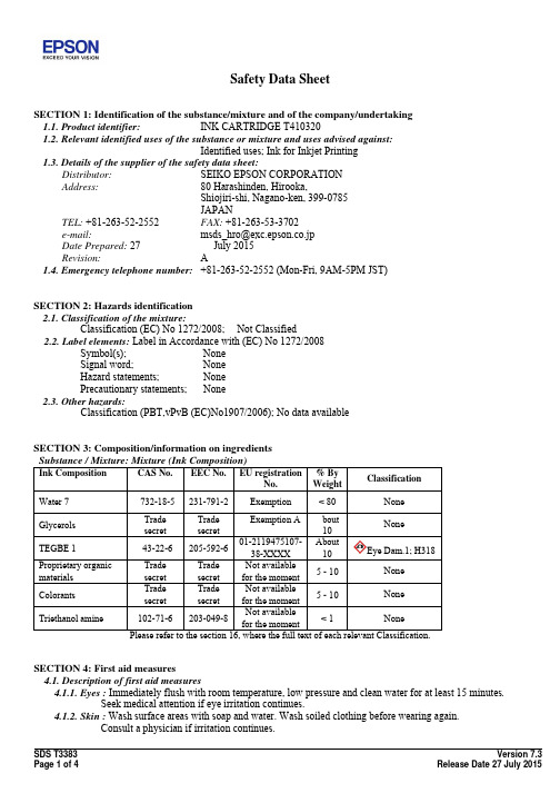
Safety Data SheetSECTION 1: Identification of the substance/mixture and of the company/undertaking 1.1. Product identifier: INK CARTRIDGE T4103201.2. Relevant identified uses of the substance or mixture and uses advised against:Identified uses; Ink for Inkjet Printing1.3. Details of the supplier of the safety data sheet:Distributor:SEIKO EPSON CORPORATIONAddress: 80 Harashinden, Hirooka,Shiojiri-shi, Nagano-ken, 399-0785JAPANTEL: +81-263-52-2552 FAX: +81-263-53-3702e-mail:Date Prepared: 27 July 2015Revision: A1.4. Emergency telephone number: +81-263-52-2552 (Mon-Fri, 9AM-5PM JST)SECTION 2: Hazards identification2.1. Classification of the mixture:Classification (EC) No 1272/2008; Not Classified2.2. Label elements: Label in Accordance with (EC) No 1272/2008Symbol(s); NoneSignal word; NoneHazard statements; NonePrecautionary statements; None2.3. Other hazards:Classification (PBT,vPvB (EC)No1907/2006); No data availableSECTION 3: Composition/information on ingredientsSubstance / Mixture: Mixture (Ink Composition)Ink Composition CAS No.EEC No. EU registrationNo.% ByWeightClassificationWater 7732-18-5 231-791-2 Exemption < 80 NoneGlycerols Tradesecret TradesecretExemption A bout10 NoneTEGBE 143-22-6 205-592-6 01-2119475107-38-XXXX About10 Eye Dam.1; H318Proprietary organic materials TradesecretTradesecretNot availablefor the moment 5 - 10 NoneColorants Tradesecret TradesecretNot availablefor the moment 5 - 10 NoneTriethanol amine 102-71-6 203-049-8 Not availablefor the moment< 1 NonePlease refer to the section 16, where the full text of each relevant Classification.SECTION 4: First aid measures4.1. Description of first aid measures4.1.1. Eyes : Immediately flush with room temperature, low pressure and clean water for at least 15 minutes.Seek medical attention if eye irritation continues.4.1.2. Skin : Wash surface areas with soap and water. Wash soiled clothing before wearing again.Consult a physician if irritation continues.4.1.3. Inhalation : Remove subject to ventilated fresh air. If not breathing, give artificial respiration right away.If breathing is difficult, give oxygen. Seek immediate medical attention.4.1.4. Ingestion : Seek medical advice; and attention if stomach continues to be upset.4.2. Most important symptoms and effects, both acute and delayed:Skin:Ink contact with skin may cause irritation, swelling or redness.4.3. Indication of any immediate medical attention and special treatment needed: Not necessarySECTION 5: Fire-fighting measures5.1. Extinguishing Media5.1.1.Suitable extinguishing media: Dry chemical , carbon dioxide or water.5.1.2.Unsuitable extinguishing media: None5.2. Special hazards arising from the substance or mixture: None5.3. Advice for firefighters: No special fire fighting procedures are required other than breathing apparatus.No special explosion hazards are known.SECTION 6: Accidental release measures6.1. Personal precautions, protective equipment and emergency procedures6.1.1.For non-emergency personnel: Eye or Skin protection required during clean-up. Use proper ventilation.6.1.2. For emergency responders: None6.2. Environmental precautions: Do not release to sewer, surface- or ground-water.6.3. Methods and material for containment and cleaning up6.3.1. Advice on how to contain a spill:Use sponges to wipe-up ink.6.3.2. Advice how to clean-up a spill: Rinse area with damp cloth.Place waste in closed container for disposal.Wash hands with soap and water.6.3.3. Any other information: Do not dispose of waste to the sewer.6.4.Reference to other sections: NoneSECTION 7: Handling and storage7.1. Precautions for safe handling7.1.1. Recommendations:Keep out of reach of children and do not drink ink. Do not dismantle cartridge7.1.2.Advice on general occupational hygiene:Avoid contact with eyes or clothing. In the case of skin contact, wash with soap and water.7.2. Conditions for safe storage, including any incompatibilities:Do not store the cartridge in high or freezing temperatures. Keep the cartridge out of direct sunlight.Do not store the cartridge with oxidizing agents or explosives.Make sure the cartridge is dry before insertion into printer housing.7.3. Specific end use(s): Not specifiedSECTION 8: Exposure controls/personal protection8.1.Control parameters: Not established8.2. Exposure Controls8.2.1. Appropriate engineering controls: Proper ventilation, in prevention8.2.2. Individual protection measures, such as personal protective equipment8.2.2.1. Use of personal protective equipment:Not required under suitable use as setting the cartridge on the printer.8.2.2.2. Detailed specification on equipment to provide adequate and suitable protection(a) eye/face protection:Not required under suitable use as setting the cartridge on the printer.(b) skin protection: hand protection & others:Not required under suitable use as setting the cartridge on the printer.(c) respiratory protection:Not required under suitable use as setting the cartridge on the printer.(d) thermal hazards: Not required under suitable use as setting the cartridge on the printer.8.2.3. Environmental exposure controls: Not establishedSECTION 9: Physical and chemical properties9.1. Information on basic physical and chemical properties:Appearance: Magenta LiquidOdour: SlightlyOdour threshold:No data availablepH: 8.5± 0.5 at 20°CMelting point / freezing point: No data availableInitial boiling point and boiling range: No data availableFlash point: Not detected until 100°C (Closed cup, ASTM D3278) Evaporation rate:No data availableFlammability (solid, gas): Not applicable (liquid)Upper/lower flammability or explosive limits:No data availableVapor pressure:No data availableVapor density: No data availableRelative density: About1.08 at 20°CSolubility(ies):CompletePartition coefficient: n-octanol/water:No data availableAuto-ignition temperature: No data availableDecomposition temperature:No data availableViscosity:Less than 5 mPa·s at 20°CExplosive properties: NoneOxidizing properties: None9.2. Other information: NoneSECTION 10: Stability and reactivity10.1. Reactivity: Stable under normal temperature10.2. Chemical stability: Stable under normal temperature10.3. Possibility of hazardous reactions:None10.4. Conditions to avoid: High and freezing temperatures10.5. Incompatible materials:Oxidizers and explosives10.6. Hazardous decomposition products: N o data availableSECTION 11: Toxicological information11.1. Information on toxicological effects:Acute toxicity:Not meet the criteria for classification according to (EC) No 1272/2008Not meet the criteria for classification according to (EC) No 1272/2008 Irritation: Eye:Not meet the criteria for classification according to (EC) No 1272/2008 Skin:Corrosivity:Not meet the criteria for classification according to (EC) No 1272/2008Not meet the criteria for classification according to (EC) No 1272/2008 Sensitisation: Skin:Carcinogenicity:Not meet the criteria for classification according to (EC) No 1272/2008Not contain any substances listed in IARC Monographs (1,2A and 2B) Mutagenicity: Not meet the criteria for classification according to (EC) No 1272/2008Negative (by Ames test)Toxicity for reproduction:Not meet the criteria for classification according to (EC) No 1272/2008SECTION 12: Ecological information12.1. Toxicity: No data available12.2. Persistence and degradability: No data available12.3. Bioaccumulative potential: No data available12.4. Mobility in soil: No data available12.5. Results of PBT and vPvB assessment: Has not carried out PBT and vPvB assessment12.6. Other adverse effects: No data availableSECTION 13: Disposal considerations13.1Waste treatment methods: Disposal should be in accordance with federal, state, and local requirements. SECTION 14: Transport information14.1. UN number: Not applicable14.2. UN proper shipping name: Not applicable14.3. Transport hazard class(es): Not applicable14.4. Packing group: Not applicable14.5. Environmental hazards:Not applicable14.6. Special precautions for user: Not applicable14.7. Transport in bulk according to Annex II of MARPOL 73/78 and the IBC Code: Not applicable SECTION 15: Regulatory information15.1. Safety, health and environmental regulations/legislation specific for the substance or mixture:EU Information:Regulation (EC) No 2037/2000: Is not subjectRegulation (EC) No 850/2004: Is not subjectRegulation (EC) No 689/2008: Is not subjectUS Information:TSCA Section 4(a) Final Test Rules Regulated: Not regulatedTSCA Section 5 Significant New Use Rule Regulation: Not regulatedTSCA Section 8(a) Preliminary Assessment Information Rule (PAIR): Not regulatedTSCA Section 12(b) One-Time Export Notification Regulated: Not regulatedCalifornia Proposition 65: Not regulatedCanada Information:WHMIS Controlled Product: Not applicable (Manufactured article)Australia Information:Statement of Hazardous Nature: Not classified as hazardous according to criteria of NOHSCNew Zealand Information:Hazardous Substances and New Organisms Act 1996: Not regulated15.2. Chemical safety assessment:This ink has not carried out any Chemical Safety Assessment yet.SECTION 16: Other informationFull text of phrases referred to in Section 3: H318 Causes serious eye damage.This “Safety Data Sheet” contains health, safety, and environmental information. It does not replace any precautionary language or use and disposal information which accompanies the product. The information contained herein is believed to be accurate at the time of preparation, but should only be used as a guide. It is subject to revision from time to time. EPSON does not warrant the completeness or accuracy of the information contained herein.。
伯乐焊材CHI

高强管道钢
API X65 X70 X80 X100-X110
EN L450MB L485MB L555MB
FOX CEL-FOX CEL+
FOX BVD RP
FOX EL 85-FOX CEL 85 G FOX BVD 85
FOX CEL-FOX CEL+
FOX BVD RP
FOX CEL 85-FOX CEL 85 G FOX BVD 90
Pipeshield 71 T8-FD
12, 18 12 - 17 13 - 19 13, 19
Pipeshield 71 T8-FD
12 - 18 14
Pipeshield 71 T8-FD
12 - 18 14 - 17
Pipeshield 71 T8-FD
12, 18 12 - 17 13 - 19 13, 19
FOX BVD RP
FOX CEL 75, FOX CEL 75 G FOX BVD 85
FOX CEL 85, FOX CEL 85 G
FOX EV Pipe
FOX EV Pipe FOX EV 60 Pipe
SG 3-P K-Nova Ni
FOX EV Pipe FOX EV 60 Pipe
SG 3-P K-Nova Ni
据当今最先进的工业特殊要求生产。 对于特定客户或特殊工艺要求,我们可提供相关文件、证书、 检验、包装与产品标识等。详细情况请与我们联系!
伯乐焊接特别领先于高温抗蠕变钢、不锈钢和镍基合金焊接 材料。相信凭借伯乐焊接80多年的经验与实践,我们可以成为 当今高要求工业用户的最佳合作伙伴。 您可以登录网站获得您附近的销售 伙伴。
天然气 4000 1016
HAT1020资料
Forward Transfer Admittance vs.
Drain Current 20
10
Tc = –25 °C
5
75 °C
2
25 °C
1
0.5
0.2 –0.2
V DS = –10 V Pulse Test
–0.5 –1 –2 –5 –10 –20 Drain Current I D (A)
Drain to Source Voltage V DS (V)
Dynamic Input Characteristics
0
0
V DD= –5 V
–10 V
–10
–25 V
–4
–20 V DS
–30
–40
V GS
V DD = –25 V –10 V –5 V
–50 I D = –5 A
0
8
16 24 32
0.01 –0.2
–0.5 –1 –2 –5 –10 –20 Drain Current I D (A)
Static Drain to Source on State Resistance R DS(on) (Ω)
Static Drain to Source on State Resistance vs. Temperature
Gate to source leak current
I GSS
Zero gate voltege drain current
I DSS
Gate to source cutoff voltage
VGS(off)
Static drain to source on state
RDS(on)
E24

*/
#include <intrins.h>
void PrintByte(unsigned char byte_data)
{
while( BUSY == 1 ){
}
PRINTER_DATA = byte_data;
nSTB = 0;
_nop_();
// 调整 nSTB 信号脉宽
nSTB = 1;
}
/*
SETB TR1
; 启动定时器 T1
14
炜煌针式打印机说明书
MOV SCON, #50H
; 设置串行口工作方式为异步串行口,模式 1
SETB TI
; 设置标志位,为发送数据作准备
RET
; 定义待打印数据内容
; 保存在程序段
print_content:
DB '北京炜煌科技微型打印机', 0DH, 'MicroPrinter demo', 0DH
该信号高电平时,表示打印机正“忙”不能接受数据,而当该信号
2
BUSY 出
低电平时,表示打印机“准备好”,可以接收数据)
6
BUSY 出 同 BUSY(TTL 电平时,此引脚为空引脚)
9
GND — 信号地
注: 1.“入”表示输入到打印机; 2.“出”表示从打印机输出 3.信号的逻辑电平为 TTL 电平。
2.1.3 并口例程
单片机控制打印机时汇编例程
BUSY
EQU P3.2
; 定义 BUSY 信号引脚
nSTB
EQU P3.7
; 定义 nSTB 信号引脚
ORG 0000H
6
0 . 5μS 0 . 5μS
start: main:
MBR10200中文资料
0.5
A V/uS
0.85 0.71 0.1 6.0 200 2.0
1.05 -
V
IR
Cj RθJC TJ TSTG
0.009 10
mA mA pF ℃/W ℃ ℃
Operating Junction Temperature Range Storage Temperature Range Notes: 1. 2.0us Pulse Width, f=1.0 KHz 2. Pulse Test: 300us Pulse Width, 1% Duty Cycle 3. Mounted on Heatsink Size of 2 in x 3 in x 0.25in Al-Plate.
25
100 150
0.1
1
10 NUMBER OF CYCLES AT 60Hz
100
FIG.3- TYPICAL INSTANTANEOUS FORWARD CHARACTERISTICS
40
FIG.4- TYPICAL REVERSE CHARACTERISTICS
50 10
INSTANTANEOUS FORWARD CURRENT. (A)
PEAK FORWARD SURGE CURRENT. (A)
AVERAGE FORWARD CURRENT. (A)
RESISTIVE OR INDUCTIVE LOAD
10
150
8
125 100
6
75 50
4 2 0 0 50 CASE TEMPERATURE. ( C)
o
MBR1035-MBR1045 MBR1050-MBR10200
100
1,000
ROHM RJP020N06 说明书
−
Turn-on delay time
td (on) ∗ −
Rise time
tr ∗ −
Turn-off delay time
td (off) ∗ −
Fall time Total gate charge Gate-source charge Gate-drain charge
tf ∗ − Qg ∗ − Qgs ∗ − Qgd ∗ −
About Export Control Order in Japan Products described herein are the objects of controlled goods in Annex 1 (Item 16) of Export Trade Control Order in Japan. In case of export from Japan, please confirm if it applies to "objective" criteria or an "informed" (by MITI clause) on the basis of "catch all controls for Non-Proliferation of Weapons of Mass Destruction.
Total power dissipation
PD
Channel temperature Range of storage temperature
∗1 Pw≤10µs, Duty cycle≤1% ∗2 When mounted on a 40+ 40+ 0.7mm ceramic board
Tch Tstg
Appendix1-Rev1.1
PDC信昌FCF高精度低温漂厚膜电阻规格书

No.220-1, Sec. 2, Nanshan Rd., Lujhu, Taoyuan 33860, Taiwan, R.O.C.SPECIFICATION FOR APPROVALDATE:信昌電子陶瓷股份有限公司CUSTOMER:PART NAME: General Purpose Lead Free &. Halogen Free Chip Resistors CUSTOMER'S DWG NO CUSTOMER'S DWG. NO.CUSTOMER'S PART NO.PDC PART NO.DESCRIPTION.FCF SERIES APPROVED" ˇ"CUSTOMER'SSIGNATURENOTEFULL APPROVEDRESULTACTIONFULL APPROVED CONDITIONAL APPROVED REJECTEDCUSTOMER SIGNATURE FOR ACCEPTANCE OUR ACTION CUSTOMER SIGNATURE FOR ACCEPTANCEPREPARED BY CHECKED BY APPROVED BYOUR ACTION SIGNATURE Jenny Tseng Tony Chou Byron TsaiEdition :F C F - R e v . 1 8 . 0 . I 4 0Serial Number : CPDC Email:sales@THICK FILMLEAD FREE CHIP RESISTORS tiConfigurationDimensionsSize L W C D 010050.40±0.020.20±0.020.08±0.030.10±0.03100202010.60±0.030.30±0.030.10±0.050.15±0.05■ Power Derating Curve(unit: mm) Maximum dissipation in percentage of Maximum dissipation in percentage ofPDCTHICK FILMLEAD FREE CHIP RESISTORS■ RatingFCF Series‧LEAD FREE CHIP RESISTORS±5%(J)10ME-24±0.1%(B)E-96±0.25%(C)E-96±0.5%(D)E-96±1%(F)E-96±1%(F)±100110M E-96±2%(G)±200110M E-24±5%(J)±20010M E-243.3M E-96/24±5%(J)0 &. 110M E-24±20050V±1%(F)1FCF0102011/20W25V1M E-96E 2410M E-9610FCF0612061/4W 1/10W150V±100±200±100SizePower Rating at 70℃04021/16WTypeE-960&11200V ±100Standard Resistance Values Max.RCWVMax. Overload VoltageResistance Tolerance (%)TemperatureCoefficient(TCR; ppm/℃)±50E-96FCF0250VFCF05FCF03±0.1%(B)±1%(F)08051/8W±0.5%(D)50V0603±100200V Resistance Range(Ω)Min.Max.11020100V100V300V400V 1M 10M 510KFCF1212101/3W 400V ±1%(F)30V100FCF0A010051/32W15V1M E-960 &. 4.791E-2491E-961M E-240 &. 10 &. 1±1%(F)±5%(J)±200±300±200±3000 &. 4.7100◎ 01005 size maximum resistance R max < 50m Ω and rated current I R ≦ 0.8A◎ 0201,0402,0603 size maximum resistance R max < 50m Ω and rated current I R ≦ 1A◎ 0805,1206,1210,2010,2512 size maximum resistance R max < 50m Ω and rated current I R ≦ 2A◎ Temperature Coefficient of Resistance for 01005,0201 = -200 ~ +600◎ Temperature Coefficient of Resistance for 0402,0603,0805,1206 = -200 ~ +400◎ Temperature Coefficient of Resistance for 2010,2512 = ±300■ Soldering Temperature CurveFCF-Rev 180I40E-24E-24E-9610M E-24FCF20200V1WJumper( 0Ω ) :FCF2525121Ω~10Ω:0 &. 1±2000 &. 110M E-96400V ±1001200V ±5%(J)±1%(F)±5%(J)±1%(F)±200±200±10010M 10M 0 &. 110M1±5%(J)400V20103/4W 0Typical values (solid line).t (s)Process limits (dotted line).WAVE soldering.20025015010050T (℃ .FCF-Rev.18.0.I402/7P D C Email:sales@THICK FILMLEAD FREE CHIP RESISTORS■ Part Number FCF 05FT1002-TypeSizeTolerancePackingGMTCRFCF0A :01005B :±0.1%S :Paper tape 1Kpcs examples:01:0201C :±0.25%T:Paper tape5Kpcs02:0402D :±0.5%V :Paper tape 10Kpcs =10K Ω03:0603F :±1%U :Paper tape 15Kpcs P :50ppm 05:0805G :±2%W :Paper tape 20Kpcs N:100ppm 06:1206J :±5%P:Plastic tape 4Kpcs For 1Ω~10Ω12:1210X :Plastic tape 8Kpcs For 06031% only.20:2010Y :Plastic tape 16KpcsE48/E9625:2512example:=10K Ω(Refer Table 1.)SPECIFICATION■ Resistance MarkingE - 24 SERIES3 digit marking for ±5% E24examples:47347× 103=47K Ω1R5=1.5ΩE - 96 SERIES4 digit marking for E96 examples:1542154× 10 2=15K4Ω22R1=22.1Ω3 digit marking for E96 - 0603examples:02C ( Table 1 )102× 10 2=10K2Ω※ No Marking of 0402、0201、01005.FCF-Rev.18.0.I403/71002:100*102FCF05FT-1002P-=10K Ω103 :10*103- TCR as Rating Table 01C:100*102PDC473154202C Email:sales@■ 0603 1% Marking Table (Table 1)CodeE48E96CodeE48E96CodeE48E96CodeE48E96011001002517817849316316735625620210226182503247457603105105271871875133233275590590041072819152340766040511011029196196533483487761961906113302005435778634071151153120520555365365796496490811832210563748066509121121332152155738338381681681101243422158392826981112712735226226594024028371571512130362326041284732131331333723723761422422857507501413738243624328676815140140392492496344244287787787161434025564453888061714714741261261654644648982582518150422676647590845191541544327427467487487918668662015844280684999288721162162452872876951151193909909221654629470523949312316916947301301715365369595395324174483097254996976Code A B C D E F G H X Y Z Multiplier 10010110 210 310 410 510 610 710-110-210-3■ Standard resistance value.FCF-Rev.18.0.I404/7PDC Email:sales@■ Tape And Reel Package‧Taping specs are according to EIA RS-481Accumulated dimensional tolerance 40±0.2mmSizeA BW FE P1P2P0010050.24±0.030.45±0.038.00±0.203.50±0.05 1.75±0.10 2.00±0.05 2.00±0.054.00±0.1002010.37±0.050.67±0.058.00±0.203.50±0.051.75±0.102.00±0.05 2.00±0.05 4.00±0.1004020.70±0.10 1.20±0.108.00±0.303.50±0.05 1.75±0.10 2.00±0.10 2.00±0.054.00±0.100603 1.10±0.20 1.90±0.208.00±0.30 3.50±0.05 1.75±0.10 4.00±0.10 2.00±0.05 4.00±0.100805 1.65±0.20 2.40±0.208.00±0.30 3.50±0.05 1.75±0.10 4.00±0.10 2.00±0.05 4.00±0.101206 2.00±0.20 3.60±0.208.00±0.30 3.50±0.05 1.75±0.10 4.00±0.10 2.00±0.05 4.00±0.101210 3.00±0.20 3.60±0.208.00±0.303.50±0.05 1.75±0.104.00±0.10 2.00±0.05 4.00±0.102010 2.80±0.205.50±0.2012.00±0.30 5.50±0.05 1.75±0.10 4.00±0.10 2.00±0.05 4.00±0.1025123.50±0.20 6.70±0.2012.00±0.305.50±0.051.75±0.104.00±0.10 2.00±0.05 4.00±0.10(unit: mm)FCF-Rev.18.0.I405/71.50+0.10/-01.50+0.10/-01.50+0.10/-0D1.50+0.10/-01.50+0.10/-01.50+0.10/-01.50+0.10/-01.50+0.10/-01.50+0.10/-0P 1ADBWEFP 2P 0PDC Email:sales@‧Reel Package(unit: mm)FCF-Rev.18.0.I406/7PDC Email:sales@■ FCF ≧ 1Ω Specification And Test MethodsSPECIFICATIONTEST METHODJ : ±5% , G: ±2% , F: ±1%D: ±0.5% , C: ±0.25% , B: ±0.1%Zero ohm Jumper <50m ΩJ 、G: △R ≦ ± (2% + 0.1Ω)F 、D: △R ≦ ± (1% + 0.05Ω)C 、B: △R ≦ ± (0.5% + 0.05Ω)Over 95% of termination must be covered with Solder J 、G: △R ≦ ± (1% + 0.1Ω)F 、D 、C 、B: △R ≦ ± (0.5% + 0.05Ω)No mechanical damageIEC 60115-1 / JIS C 5201-1 , Clause 4.8Test temperature :25℃ (T1) → -55℃ (T2)25℃ (T1) → +155℃ (T2)R2-R11R1T2-T1T1: 25℃ T2: Test temperatureR1: Resistance at reference temperature (T1) R2: Resistance at test temperature (T2)J 、G: △R ≦ ± (3% + 0.1Ω)F 、D: △R ≦ ± (1% + 0.05Ω)C 、B: △R ≦ ± (0.5% + 0.05Ω)J 、G: △R ≦ ± (3% + 0.1Ω)F 、D: △R ≦ ± (1% + 0.05Ω)C 、B: △R ≦ ± (0.5% + 0.05Ω) J 、G: △R ≦ ± (1% + 0.1Ω)F 、D 、C 、B: △R ≦ ± (0.5% + 0.05Ω)No mechanical damageBetween termination and coatingmust be over 1000M Ω J 、G: △R ≦ ± (1% + 0.1Ω)F 、D 、C 、B: △R ≦ ± (0.5% + 0.05Ω)No mechanical damageFCF-Rev.18.0.I40Bending StrengthIEC 60115-1 / JIS C 5201-1 , Clause 4.33Resistance change after bended on the 90mm PCB.Bend: 3mm for 01005、0201、0402、0603、08052mm for 1206、1210、2010、25127/7Temperature CycleIEC 60115-1 / JIS C 5201-1 , Clause 4.19Repeat 5 cycles as follows-55℃(30 min.) + 25℃(2~3 min.)+155℃(30 min.) + 25℃(2~3 min.)Insulation ResistanceIEC 60115-1 / JIS C 5201-1 , Clause 4.6Test voltage: 100±15VLoad LifeIEC 60115-1 / JIS C 5201-1 , Clause 4.25Permanent resistance change after 1000+48/-0 hours (1.5 hours ON , 0.5 hour OFF) at RCWV or Max.Keep the resistor at 70±2℃ ambient×10 6Load Life HumidityIEC 60115-1 / JIS C 5201-1 , Clause 4.24Maintain the temperature of the resistor at 40±2℃and 90~95% R.H. with the rated voltage applied.Cycle ON for 1.5 hours and OFF for 0.5 hour for 1000+48/-0hours. After 1~4 hour, measure the resistance value.Temperature Coefficient of Resistance (TCR)Refer to the rating table information.TCR (ppm/℃) =×SolderabilityIEC 60115-1 / JIS C 5201-1 , Clause 4.17After immersing flux, dip in the245±2℃ molten solder bath for 3±0.5 sec Resistance to Solder HeatIEC 60115-1 / JIS C 5201-1 , Clause 4.18With 260±5℃ for 10±1 sec.ITEM DC Resistance IEC 60115-1 / JIS C 5201-1 , Clause 4.5Measure the resistance value.Short time Overload IEC 60115-1 / JIS C 5201-1 , Clause 4.132.5×Rated voltage or Max. Overload Voltage for 5 sec.measure resistance after 30 minutes PDC Email:sales@。
BRM-1040-3-FB4.0中文资料
BRIGHT LED ELECTRONICS CORP.
SINCE 1981
BRM-1040-3-FB4.0
● Electrical And Optical Curves(Ta=25℃)
Fig.4 Relative Spectral Sensitivity vs.
(%) 1.2
Fig.5 Relative Transmission Distance vs. Direction
Fig.3 Measuring System
+ 10uF
Standard Transmitter Standard Transmitter
θ θ
Vcc
D.U.T
GND
Vout
100kΩ
Vout
Vout Oscilloscope Oscilloscope
Ver:1.0 Page: 3 of 5
元器件交易网
Fig.8 Frequency Dependence of Responsivity
(m) 1.0 20
Fig.9 Arrival Distance Vs. Ambient Temperature
0.8
16
Transmission Distance
0
0.6
12
Rel. Responsitivity
0.4
0 10 20 30
Wavelength
1.0
Relative Responsitibity
0.8
1.0
40
0.6
0.9 0.8
50 60 70
0.4
0.2
0.7
80 90
0 750
850
950
BAM-1020资料
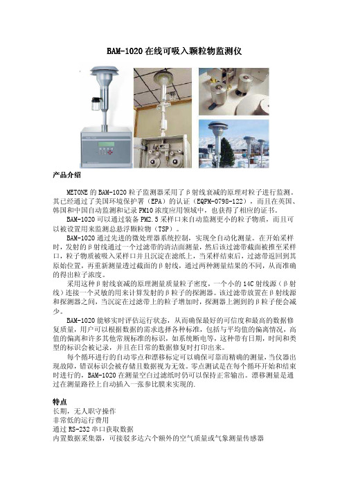
BAM--1020在线可吸入颗粒物监测仪BAM产品介绍产品介绍METONE的BAM-1020粒子监测器采用了β射线衰减的原理对粒子进行监测。
其已经通过了美国环境保护署(EPA)的认证(EQPM-0798-122),而且在英国、韩国和中国自动监测和记录PM10浓度应用领域中,也获得了相应的证书。
BAM-1020可以通过装备PM2.5采样口来自动监测更小的粒子物质,而且可以被设置用来监测总悬浮颗粒物(TSP)。
BAM-1020通过先进的微处理器系统控制,实现全自动化测量。
在开始采样时,发射的β射线通过一个过滤带的清洁面测量,然后该过滤带截面被推至采样口,粒子物质被吸入采样口并且沉淀在滤纸上,当采样结束后,过滤带返回到其原始位置,再重新测量透过截面的β射线,通过两种测量结果的不同,从而准确的得出粒子浓度。
采用这种β射线衰减的原理测量质量粒子密度,一个小的14C射线源(β射线)连接一个灵敏的用来计算发射的β粒子的探测器。
该过滤带放置在β射线源和探测器之间,当沉淀在过滤带上的粒子增加时,探测器上测到的β粒子便会减少。
BAM-1020能够实时评估运行状态,从而确保最好的可信度和最高的数据修复质量,用户可以根据数据的需求选择各种标准,包括与平均值的偏离情况,高值的偏离和许多其他常规标准的标识,如系统断电等,这种带有日期,时间和类型的标识会被记录,并且在日常的数据修复时打印出来。
每个循环进行的自动零点和漂移标定可以确保可靠而精确的测量,当仪器出现故障,错误标识会被存储且数据视为无效。
零点测试是在每个循环开始和结束时进行的,BAM-1020在测量空白过滤纸时仍可以保持正常输出。
漂移测量是通过在测量路径上自动插入一张参比膜来实现的.特点特点长期,无人职守操作非常低的运行费用通过RS-232串口获取数据内置数据采集器,可接驳多达六个额外的空气质量或气象测量传感器定时(一小时)自动“零漂移”检测Metone公司“MicroMet Plus”或“Air Plus”软件操作针对TSP、SCC-PM2.5、WINS-PM2.5不同直径粒子,可选采样口可获取一小时或二十四小时平均值技术参数技术参数范围 0~0.1,0.2,0.25,0.5,1.0,2.0,5.0,10mg/m3循环 1小时测量分辨率 0.1 µg/m3显示分辨率 1 μg/m3精度 读数的±8%,(1小时模式时);±2%相对于FRM (24小时模式时)Beta源 14C,60μCi过滤带 玻璃纤维材料流速 0~20SLM(用户可调)数据存储 200天(1小时采样)BAM过滤带 PN460130,长21米认证 CE, NRC, TUV, California ARB, ISO 9001电源 100~230VAC,50/60Hz温度范围 -30℃~60℃(0~90%RH,无冷凝)重量 24.5kg尺寸 310mm×430mm×400mm。
FM1020资料

元器件交易网
Chip Schottky Barrier Diodes
FM1020 THRU FM1040
Silicon epitaxial planer type
Formosa MS
SMC
0.276(7.0) 0.260(6.6) 0.012(0.3) Typ.
Features
0.032(0.8) Typ. 0.040(1.0) Typ. 0.152(3.8) 0.144(3.6)
0.189(4.8) 0.173(4.4)
0.244(6.2) 0.228(5.8)
0.087(2.2) 0.071(1.8)
0.040 (1.0)Байду номын сангаасTyp.
Mechanical data
Case : Molded plastic, JEDEC DO-214AB Terminals : Solder plated, solderable per MIL-STD-750, Method 2026 Polarity : Indicated by c athode band Mounting P osition : Any Weight : 0.00585 ounce, 0.195 gram
BRN常用型号自动化元件介绍
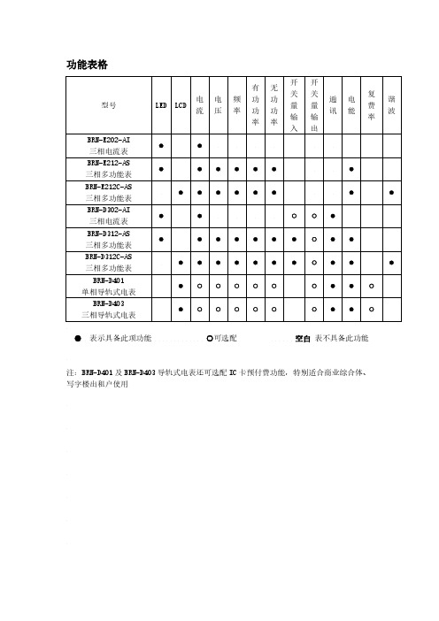
功能表格●表示具备此项功能○可选配空白表不具备此功能注:BRN-D401及BRN-D403导轨式电表还可选配IC卡预付费功能,特别适合商业综合体、写字楼出租户使用BRN-E202/D302–AI三相多功能表一、主要功能:●LED显示●三相电流测量注:BRN-E202-AI不带通讯功能,不带开关量功能BRN-D302-AI带通讯,可选配开关量功能。
三、开孔尺寸85*85mm一、主要功能●LED显示●三相电压,三相电流,频率,三相有功功率、无功功率,功率因数,三相电能●2路隔离型开关量输入●RS485/MODBUS通讯注:BRN-E212-AS不带通讯功能,不带开关量功能;BRN-D312-AS带通讯,标配两路开关量输入,可选配两路开关量输出。
76*76mmBRN-E212C/D312C-AS三相多功能表一、主要功能●LCD显示●三相电压,三相电流,频率,三相有功功率、无功功率,功率因数,三相电能●2路隔离型开关量输入●可选配2-31次谐波测量●RS485/MODBUS通讯●注:BRN-E212C-AS不带通讯功能,不带开关量功能;●BRN-D312C-AS带通讯,标配两路开关量输入,可选配两路开关量输出。
三、开孔尺寸76*76mmBRN-D401单相导轨式电能表Array一、主要功能●LCD显示●单相电能●可直接接入最大80A电流,也可外接电流互感器●RS485/MODBUS通讯●可选配复费率功能●可选配开关量输出型号(内置磁保持继电器),80A以内可直接分闸/合闸,可远程遥控,特别适用于学校及宿舍管理●可选配IC卡预付费功能(内置IC识别模块及磁保持继电器),电费余额不足可自动断电,适用于写字楼及商铺出租项目。
三、安装方式35mm导轨/4P宽度一、主要功能●LCD显示●三相电能●可直接接入最大80A电流,也可外接电流互感器●RS485/MODBUS通讯●可选配复费率功能●可选配开关量输出型号(内置磁保持继电器),80A以内可直接分闸/合闸,可远程遥控,特别适用于学校及宿舍管理●可选配IC卡预付费功能(内置IC识别模块及磁保持继电器),电费余额不足可自动断电,适用于写字楼及商铺出租项目。
Belden FiberExpress 12-Fiber 奥姆3 OM3 OFCR 纤维光纤分布线说
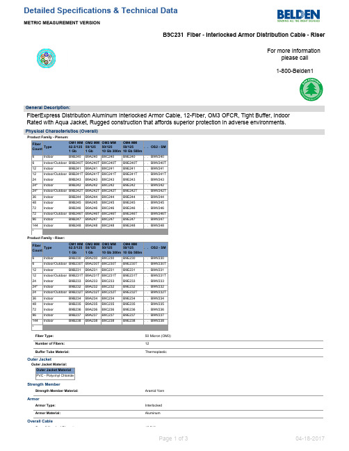
No
Suitability - Burial:
No
Sunlight Resistance:
No
Plenum/Non-Plenum
Plenum (Y/N):
No
Optical Characteristics (Overall)
Maximum Attenuation @ 850nm:
Maximum Attenuation @ 1300nm:
OM4 MM 50/125
. . OS2 - SM
1 Gb
1 Gb
10 Gb 300m 10 Gb 500m
6
Indoor
B9B230 B9A230 B9C230
B9E230
. . B9W230
6
Indoor/Outdoor B9B230T B9A230T B9C230T B9E230T . . B9W230T
96 Indoor
B9B247 B9A247 B9C247
B9E247
. . B9W247
144 Indoor
B9B248 B9A248 B9C248
B9E248
. . B9W248
*
Product Family - Riser:
Fiber Type Count
OM1 MM OM2 MM OM3 MM 62.5/125 50/125 50/125
24 Indoor
B9B243 B9A243 B9C243
B9E243
. . B9W243
24* Indoor
B9B242 B9A242 B9C242
B9E242
. . B9W242
24* Indoor/Outdoor B9B242T B9A242T B9C242T B9E242T . . B9W242T
- 1、下载文档前请自行甄别文档内容的完整性,平台不提供额外的编辑、内容补充、找答案等附加服务。
- 2、"仅部分预览"的文档,不可在线预览部分如存在完整性等问题,可反馈申请退款(可完整预览的文档不适用该条件!)。
- 3、如文档侵犯您的权益,请联系客服反馈,我们会尽快为您处理(人工客服工作时间:9:00-18:30)。
Fig.8 Frequency Dependence of Responsivity
(m) 1.0 20
Fig.9 Arrival Distance Vs. Ambient Temperature
0.8
16
0.6
Transmission Distance
0
12
Rel. Responsitivity
0.4
元器件交易网
BRIGHT LED ELECTRONICS CORP.
SINCE 1981
BRM-1020-2-FB4.3
INFRARED RECEIVER MODULE
● Description
1. The BRM-1020-2-FB4.3 is miniaturized infrared receiver for remote control and other applications requiring improved ambient light rejection. 2. The separate PIN diode and preamplifier IC are assembled on a single lead frame. 3. The epoxy package contains a special IR filter. 4. This module has excellent performance even in disturbed ambient light applications and provides
Fig.1 Transmitter Wave Form Transmitter Output
D.U.T Output Pulse VH TL TH VL
600us
600us
Fig.2 Measuring Method Measuring Method 20cm
>10kΩ 5.0± 0.1V
Fig.3 Measuring System
—
Storage Temperature
Tstg
-40~+85
— 4mm from mold body less than 5 sec
Soldering Temperature
Tsol
260
Electrical And Optical Characteristics(Ta=25℃)
Parameter
SINCE 1981
BRM-1020-2-FB4.3
Electrical And Optical Curves(Ta=25℃)
Fig.4 Relative Spectral Sensitivity vs.
(%) 1.2
Fig.5 Relative Transmission Distance vs. Direction
SINCE 1981
BRM-1020-2-FB4.3
Packaging Box Dimensions
Packaging Bag Dimensions
Notes:
1、150pcs per bag, 1.5Kpcs per box. 2、All dimensions are in millimeters(inches). 3、Specifications are subject to change without notice.
8
0.2
0
4
0.0 0.7
0 0.8 0.9 1.0 1.1 1.2 1.3 -40 -20 0 20 40 60 80 100 (° C)
Relative Frequency
Ambient Temperature
REV: 1.0 Page: 4 of 4
元器件交易网
BRIGHT LED ELECTRONICS CORP.
10000 (mW/cm )
2
1.2 1.0 0.8 0.6 0.4
0.4
0.2
=950nm,Optical Test Signal,Fig.8
0.2 0.0 0.1 0.0 -30 0 30 60 90 (° C) 1 10 100 1000
Irradiance
Ambient Temperature
1.All dimensions are in millimeters (inches). 2.Tolerance is ±0.10mm (0.004’’) unless otherwise specified. 3.Specifications are subject to change without notice.
元器件交易网
BRIGHT LED ELECTRONICS CORP.
SINCE 1981
BRM-1020-2-FB4.3
Application Circuit
47Ω Infrared Emitting Diode IRM Vcc Out GND
GND +5V
47uF
>10kΩ uC
Unit
V mA
Reception Distance
L In the range of 45°cone — — — —
m
B.P.F Center Frequency Peak Wavelength Half Angle
fo λp θ
— — — Specified by the output TH period within a range from 10cm to the arrival distance (average value of 50 pulses) Specified by the output TL period within a range from 10cm to the arrival distance (average value of 50 pulses) 10cm over the ray axis 10cm over the ray axis
0 10 20 30
Wavelength
1.0
Relative Responsitibity
0.8
1.0
40
0.6
0.9 0.8
50 60 70
0.4
0.2
0.7
80 90
0 750
850
950
1050
1150 (nm)
0.5
0.3
0.1
0.2
0.4
0.6
Wavelength
Relative Transmission Distance
Vcc
+ 10uF
Standard Transmitter Standard Transmitter D.U.T GND
Vout
100kΩ
Vout
Vout Oscilloscope Oscilloscope
REV: 1.0 Page: 3 of 4
元器件交易网
BRIGHT LED ELECTRONICS CORP.
KHz nm deg
High Level Pulse Width
TH
400
—
800
µS
Low Level Pulse Width
TL
400
—
800
µS
High Level Output Voltage Low Level Output Voltage
VH VL
4.5 —
— —
— 0.5
V V
REV: 1.0 Page: 2of 4
Supply Voltage Supply Current
Symbol
Vcc Icc
Condition
DC voltage No signal input At the ray axis
Min.
2.7 — 12 6 — — —
Ratings Typ. Max.
— — — — 38 940 45 5.5 1.5 —
1.45(.057) 3.85(.152) 7.4(.292) 2.4(.095)
●Package Dimensions:
protection against uncontrolled output pulses.
● Features
1. 2. 3. 4. 5. 6. 7. Photo detector and preamplifier in one package . Internal filter for PCM frequency. High immunity against ambient light.
● BLOCK DIAGRAM
Vcc Vout Limiter B.P.F PD ABLC
Demodulator
Preamp
Amp
Integrator
Comparator GND
REV: 1.0 Page: 1of 4
元器件交易网
BRIGHT LED ELECTRONICS CORP.
2.54(.10)
● Applications:
1. It can be used for TVs、VTRs、audio equipment air conditioners、 car stereo radio、toys、 home computers and all other equipment requiring remote control.
(mS) 1.0
Fig.6 Output Pulse Diagram
(mA) 2.0 1.8
Fig.7 Supply Current vs. Ambient Temperature
0.8
on
1.6 1.4