HSMP-381A中文资料
费思FT6300A系列中小功率电子负载用户手册适用型号(FT6301A-FT6306A)

安全摘要
在操作和维修电子负载过程中,请严格遵守以下安全须知。不遵守以下注意事项或本手册中其它章节 提示的特定警告,可能会削弱本负载所提供的保护功能。对于用户不遵守这些注意事项而造成的后果,费 思科技不负任何责任。
目录 ....................................................................................................................................................... IV
II
安全标识
在本产品外壳、用户手册所使用国际符号的解释请参见下表。
III
目录
前言........................................................................................................................................... I 通告........................................................................................................................................... I
第 2 章 安装.......................................................................................................................................... 11
HSMP-3892中文资料

Surface Mount PIN Diodes Technical DataFeatures•Diodes Optimized for:Low Current SwitchingLow Distortion AttenuatingUltra-Low DistortionSwitchingMicrowave FrequencyOperation•Surface Mount SOT-23 and SOT-143 PackagesSingle and Dual VersionsTape and Reel OptionsAvailable•Low Failure in Time (FIT) Rate[1]Note:1.For more information see theSurface Mount PIN Reliability Data Sheet.HSMP-38XX andHSMP-48XX SeriesPackage Lead CodeIdentificationrequired. The HSMP-48XX seriesare special products featuringultra low parasitic inductance inthe SOT-23 package, specificallydesigned for use at frequencieswhich are much higher than theupper limit for conventionalSOT-23 PIN diodes. TheHSMP-4810 diode is a low distor-tion attenuating PIN designed foroperation to 3 GHz. TheHSMP-4820 diode is ideal forlimiting and low inductanceswitching applications up to1.5GHz. The HSMP-4890 isoptimized for low current switch-ing applications up to 3 GHz.The HSMP-386X series of generalpurpose PIN diodes are designedfor two classes of applications.The first is attenuators wherecurrent consumption is the mostimportant design consideration.The second application for thisseries of diodes is in switcheswhere low cost is the drivingissue for the designer.The HSMP-386X series TotalCapacitance (C T) and TotalResistance (R T) are typicalspecifications. For applicationsthat require guaranteed perfor-mance, the general purposeHSMP-383X series is recom-Description/Applications The HSMP-380X and HSMP-381X series are specifically designed for low distortion attenuator applica-tions. The HSMP-382X series is optimized for switching applica-tions where ultra-low resistance is required. The HSMP-3880 switch-ing diode is an ultra low distortion device optimized for higher power applications from 50 MHz to1.5GHz. The HSMP-389X series is optimized for switching applica-tions where low resistance at low attenuators, the HSMP-380X or -381X series are recommended. For high performance switching applications, the HSMP-389X series is recommended.A SPICE model is not available for PIN diodes as SPICE does not provide for a key PIN diode characteristic, carrier lifetime.Absolute Maximum Ratings [1] T A = 25°CSymbol ParameterUnits Absolute Maximum I f Forward Current (1 ms Pulse)Amp 1P t Total Device Dissipation mW [2]250P iv Peak Inverse Voltage —Same as V BRT j Junction Temperature °C 150T STGStorage Temperature°C-65 to 150Notes:1.Operation in excess of any one of these conditions may result in permanent damage to this device.2.CW Power Dissipation at T LEAD = 25°C. Derate to zero at maximum rated temperature.PIN Switching DiodesElectrical Specifications T A = 25°CNearest Maximum Equivalent Minimum Maximum Maximum Shunt Mode Part Package Axial Lead Breakdown Series Total Harmonic Number Marking LeadPart No.Voltage Resistance Capacitance Distortion HSMP-Code [1]Code Configuration 5082-V BR (V)R S (Ω)C T (pF)Hmd (dBc)3820F00Single 3188500.6*0.8*—3822F22Series3823F33Common Anode 3824F44Common Cathode 3880S00Single—100 6.50.40–553890G00Single —1002.50.30**—3892G22Series3893G33Common Anode 3894G44Common Cathode 3895G55Unconnected PairTest ConditionsV R = V BR I F = 5 mA V R = 50 V 2 f o, Z o = 50 W Measure f = 100 MHz f = 1 MHz f o = 400 MHz I R ≤ 10 µA I F = 10 mA*V R = 20 V*P in = +30 dBm V R = 5 V**0 V biasPIN Attenuator DiodesElectrical Specifications T A = 25°C (Each Diode)NearestEquivalent Minimum Maximum Maximum Minimum Maximum Part Package Axial Lead Breakdown Series Total High Low Number Marking LeadPart No.Voltage Resistance Capacitance Resistance Resistance HSMP-Code [1]Code Configuration 5082-V BR (V)R S (Ω)C T (pF)R H (Ω)R L (Ω)3800D00Single 30801002.00.37100083802D22Series3804D44Common Cathode 3810E00Single 3081100 3.00.351500103812E22Series3813E33Common Anode 3814E44Common CathodeTest ConditionsV R = V BR I F = 100 mA V R = 50 V I F = 0.01 mA I F = 20 mA Measure f = 100 MHz f = 1 MHz f = 100 MHz f= 100 MHzI R ≤ 10 µAPIN General Purpose Diodes, Electrical Specifications T A = 25°CNearestEquivalent Minimum Maximum Maximum Part Package Axial Lead Breakdown Series Total Number Marking Lead Part No.Voltage Resistance Capacitance HSMP-Code[1]Code Configuration5082-V BR (V)R S (Ω)C T (pF) 3830K00Single3077200 1.50.3 3832K22Series3833K33Common Anode3834K44Common CathodeTest Conditions V R = V BR I F = 100 mA V R = 50 VMeasure f = 100 MHz f = 1 MHzI R≤ 10 mAHigh Frequency (Low Inductance, 500 MHz – 3 GHz) PIN Diodes, Electrical Specifications T A = 25°CMinimum Maximum Typical Maximum TypicalBreak-Series Total Total Total Part Package down Resis-Capaci-Capaci-Induc-Number Marking Lead Config-Voltage tance tance tance tance Appli-HSMP-Code Code uration V BR (V)R S (Ω)C T (pF)C T (pF)L T (nH)cation 4810EB B Dual100 3.00.350.4 1.0Attenu-Cathode ator 4820FA A Dual Anode500.6*0.75* 1.0 1.0*Limiter 4890GA A Dual Anode100 2.5**0.330.375 1.0SwitchV R = V BR I F = 100 mA V R = 50 V V R = 50 V f = 500 MHz –Measure I F = 10 mA* f = 1 MHz f = 1 MHz 3 GHzI R≤ 10 µA I F = 5 mA**V R = 20 V*V R = 0 V V R = 20 V*PIN General Purpose Diodes, Typical Specifications T A = 25°CCode Minimum Typical Series Typical Total Part Number Marking Lead Breakdown Resistance Capacitance HSMP-Code[1]Code Configuration Voltage V BR (V)R S (Ω)C T (pF)3860L00Single50 3.0/1.5*0.203862L22Series3863L33Common Anode3864L44Common CathodeTest Conditions V R = V BR I F = 10 mA V R = 50 VMeasure f = 100 MHz f = 1 MHzI R≤ 10 µA*I F = 100 mATypical Parameters at T A = 25°CPart Number Series Resistance Carrier Lifetime Reverse Recovery Time Total Capacitance HSMP-R S (Ω)τ (ns)T rr (ns)C T (pF)380X5518005000.32 @ 50 V381X7515003000.27 @ 50 V382X 1.570*70.60 @ 20 V383X20500800.20 @ 50 V388X 3.825005500.30 @ 50 V389X 3.8200*–0.20 @ 5 V Test Conditions I F = 1 mA I F = 50 mA V R = 10 Vf = 100 MHz I R = 250 mA I F = 20 mAI F = 10 mA*I F = 10 mA*90% RecoveryI R = 6 mA*Typical Parameters at T A = 25°C (unless otherwise noted), Single DiodeFigure 2. RF Capacitance vs. Reverse Bias, HSMP-3830 Series.0.150.300.250.200.350.400.45T O T A L C A P A C I T A N C E (p F )REVERSE VOLTAGE (V)Figure 1. RF Capacitance vs. Reverse Bias, HSMP-3810 Series.Figure 3. Resistance at 25°C vs. Forward Bias Current.0.150.300.250.200.35T O T A L C A P A C I T A N C E (p F )REVERSE VOLTAGE (V)R E S I S T A N C E (O H M S )I F – FORWARD BIAS CURRENT (mA)0.010.11101000.010.1110100R F R E S I S T A N C E (O H M S )I F – FORWARD BIAS CURRENT (mA)R F R E S I S T A N C E (O H M S )0.010.1110100I F – FORWARD BIAS CURRENT (mA)Figure 5. RF Resistance vs. Forward Bias Current for HSMP-3810/HSMP-4810.V R – REVERSE VOLTAGE (V)C A P A C I T A N C E (p F )Figure 6. Capacitance vs. Reverse Voltage.Figure 4. RF Resistance vs. Forward Bias Current for HSMP-3800.100010010DIODE RF RESISTANCE (OHMS)Figure 7. 2nd Harmonic Input Intercept Point vs. Diode RFResistance for Attenuator Diodes.I N P U T I N T E R C E P T P O I N T (d B m )12011511010510095908511030I F – FORWARD BIAS CURRENT (mA)Figure 8. 2nd Harmonic Input Intercept Point vs. Forward Bias Current for Switch Diodes.I N P U T I N T E R C E P T P O I N T (d B m )FORWARD CURRENT (mA)Figure 9. Reverse Recovery Time vs. Forward Current for Various Reverse Voltages. HSMP-3820 Series.T r r – R E V E R S E R E C O V E R Y T I M E (n s )110100102030V R = 2V V R = 5VV R = 10VHSMP-382XTypical Parameters (continued)100010010102030T r r - R E V E R S E R E C O V E R Y T I M E (n S )FORWARD CURRENT (mA)Figure 10. Reverse Recovery Time vs. Forward Current for Various Reverse Voltage. HSMP-3830 Series.HSMP-3830V R = 5VV R = 10V V R = 20VR E V E R S E R E C O V E R Y T I M E (n S )FORWARD CURRENT (mA)Figure 11. Typical Reverse Recovery Time vs. Reverse Voltage. HSMP-3880 Series.1020152530T R R - R E V E R S E R E C O V E R Y T I M E (n S )FORWARD CURRENT (mA)Figure 12. Typical Reverse Recovery Time vs. Reverse Voltage. HSMP-3890 Series.1001010.10.01I F – F O R W A R D C U R R E N T (m A )I F – F O R W A R D C U R R E N T (m A )V F – FORWARD VOLTAGE (mA)Figure 14. Forward Current vs. Forward Voltage. HSMP-3810 and HSMP-4810 Series.V F – FORWARD VOLTAGE (mA)Figure 15. Forward Current vs. Forward Voltage. HSMP-3820 and HSMP-4820 Series.1001010.10.01I F – F O R W A R D C U R R E N T (m A )V F – FORWARD VOLTAGE (mA)Figure 16. Forward Current vs.Forward Voltage. HSMP-3830 Series.00.20.40.60.81.01.2I F – F O R W A R D C U R R E N T (m A )V F – FORWARD CURRENT (mA)Figure 17. Forward Current vs.Forward Voltage. HSMP-3880 Series.0.20.40.60.81.01.2V F – FORWARD VOLTAGE (mA)Figure 18. Forward Current vs. Forward Voltage. HSMP-3890 and HSMP-4890 Series.Typical Parameters (continued)Figure 19. Typical RF Resistance vs. Forward Bias Current for HSMP-3860.Figure 20. Forward Current vs. Forward Voltage for HSMP-3860.Figure 21. Typical Capacitance vs. Reverse Bias for HSMP-3860.10001R E S I S T A N C E (O HM S )BIAS CURRENT (mA)10100I F – F O R W A R D C U R R E N T (m A )V F – FORWARD VOLTAGE (V)0200.515C T – C A P A C I T A N C E (p F )V R – REVERSE VOLTAGE (V)0.20.41050.10.30.12 pF** Measured at -20 V C p 0.08 pFR j = 12ΩI 0.9C T = C P + C jI = Forward Bias Current in mAEquivalent Circuit ModelHSMS-3860Typical Applications for Multiple Diode ProductsRF COMMONRF 1RF 1Figure 24. Switch Using Both Positive and Negative Bias Current.Figure 25. Very High Isolation SPDT Switch, Dual Bias.Typical Applications for Multiple Diode Products (continued)INPUT RF IN/OUTFigure 26. Four Diode π Attenuator.Figure 27. High Isolation SPST Switch (Repeat Cells as Required).VOLTAGEBIASFigure 28. Power Limiter Using HSMP-3822Diode Pair.Typical Applications for HSMP-48XX Low Inductance SeriesFigure 29. Internal Connections.HSMP-4820 & HSMP-4890HSMP-48100.5 nH*0.8pF TYPICAL FOR HSMP-3820Figure 30. Equivalent Circuit.*0.8 pF TYPICAL FOR HSMP-3820Figure 32. Equivalent Circuit.Figure 31. Circuit Layout.Microstrip SeriesConnection for HSMP-48XX SeriesIn order to take full advantage of the low inductance of the HSMP-48XX series when using them in series application,both lead 1 and lead 2 should beconnected together, as shown above.Microstrip Shunt Connections for HSMP-48XX SeriesIn the diagram above, the center conductor of themicrostrip line is interrupted and leads 1 and 2 of theHSMP-38XX series diode are placed across the resulting gap. This forces the 0.5 nH lead inductance of leads 1 and 2 to appear as part of a low pass filter, reducing the shunt parasitic inductance andincreasing the maximumavailable attenuation. The 0.3 nH of shunt inductance external to the diode is created by the via holes, and is a good estimate for 0.032" thick material.Co-Planar Waveguide Shunt Connection for HSMP-48XX SeriesCo-Planar waveguide, with ground on the top side of the printed circuit board, is shownin the diagram above. Since it eliminates the need for via holes to ground, it offers lower shunt parasitic inductance and higher maximum attenuation whencompared to a microstrip circuit.GROUND BY TWOVIA HOLES*0.8 pF TYPICAL FOR HSMP-4820Figure 34. Equivalent Circuit.Figure 33. Circuit Layout.*0.8 pF TYPICAL FOR HSMP-4820Figure 36. Equivalent Circuit.Figure 35. Circuit Layout.11Package DimensionsOutline 23 (SOT-23)PC Board FootprintsSOT-23Package CharacteristicsLead Material......................................................................................Alloy 42Lead Finish............................................................................Tin-Lead 85-15%Maximum Soldering Temperature..............................260°C for 5 seconds Minimum Lead Strength..........................................................2 pounds pull Typical Package Inductance ..................................................................2 nH Typical Package Capacitance ..............................0.08 pF (opposite leads)SOT-143Outline 143 (SOT-143)SIDE VIEWEND VIEWDIMENSIONS ARE IN MILLIMETERS (INCHES)DIMENSIONS ARE IN MILLIMETERS (INCHES)PACKAGE MARKING/go/rfFor technical assistance or the location of your nearest Hewlett-Packard salesoffice, distributor or representative call:Americas/Canada: 1-800-235-0312 or 408-654-8675Far East/Australasia: Call your local HP sales office.Japan: (81 3) 3335-8152Europe: Call your local HP sales office.Data subject to change.Copyright © 1999 Hewlett-Packard Co.Obsoletes 5968-3435E5968-5439E (6/99)Profile Option Descriptions-BLK = Bulk-TR1 = 3K pc. Tape and Reel, Device Orientation; See Figures 37 and 38-TR2 = 10K pc. Tape and Reel, Device Orientation; See Figures 37 and 38Tape and Reeling conforms to Electronic Industries RS-481, “Taping of Surface Mounted Components for Automated Placement.”Ordering InformationSpecify part number followed by option under. For example:H SMP -38XX -XXXBulk or Tape and Reel OptionPart NumberSurface Mount PIN Diode Hewlett-PackardUSER FEEDEND VIEWTOP VIEW Figure 37. Options -TR1, -TR2 for SOT-23 Packages.Figure 38. Options -TR1, -TR2 for SOT-143 Packages.END VIEWTOP VIEW。
HSMP-3814中文资料

Surface Mount RF PIN Low Distortion Attenuator DiodesTechnical DataFeatures•Diodes Optimized for:–Low Distortion Attenuating –Microwave FrequencyOperation•Surface Mount Packages–Single and Dual Versions–Tape and Reel OptionsAvailable•Low Failure in Time (FIT) Rate[1]•Lead-free Option Available Note:1.For more information see theSurface Mount PIN Reliability Data Sheet.HSMP-381x Series andHSMP-481x SeriesPackage Lead CodeIdentification, SOT-23(Top View)Description/Applications The HSMP-381x series is specifically designed for low distortion attenuator applica-tions. The HSMP-481x products feature ultra low parasitic inductance in the SOT-23 and SOT-323 packages. They are specifically designed for use at frequencies which are much higher than the upper limit for conventional diodes.A SPICE model is not available for PIN diodes as SPICE does not provide for a key PIN diode characteristic, carrier lifetime.SERIESSINGLEPackage Lead CodeIdentification, SOT-323(Top View)Absolute Maximum Ratings[1] T C = +25°CSymbol Parameter Unit SOT-23SOT-323I f Forward Current (1 µs Pulse)Amp11P IV Peak Inverse Voltage V Same as V BR Same as V BRT j Junction Temperature°C150150T stg Storage Temperature°C-65 to 150-65 to 150θjc Thermal Resistance[2]°C/W500150Notes:1.Operation in excess of any one of these conditions may result in permanent damage tothe device.2.T C = +25°C, where T C is defined to be the temperature at the package pins wherecontact is made to the circuit board.Electrical Specifications T C = +25°C (Each Diode)Conventional DiodesMinimum Maximum Maximum Minimum Maximum Part Package Breakdown Total Total High Low Number Marking Lead Voltage Resistance Capacitance Resistance Resistance HSMP-Code Code Configuration V BR (V)R T (Ω)C T (pF)R H (Ω)R L (Ω)3810E0[1]0Single100 3.00.35150010 3812E2[1]2Series3813E3[1]3Common Anode3814E4[1]4Common Cathode381B E0[2]B Single381C E2[2]C Series381E E3[2]E Common Anode381F E4[2]F Common CathodeTest Conditions V R = V BR I F = 100 mA V R = 50 V I R = 0.01 mA I F = 20 mAMeasure f = 100 MHz f = 1 MHz f = 100 MHz f= 100 MHzI R≤ 10 µAHigh Frequency (Low Inductance, 500 MHz – 3 GHz) PIN DiodesMinimum Maximum Typical Maximum Typical Part Package Breakdown Series Total Total Total Number Marking Lead Voltage Resistance Capacitance Capacitance Inductance HSMP-Code Code Configuration V BR (V)R S (Ω)C T (pF)C T (pF)L T (nH)4810EB B[1]Dual Cathode100 3.00.350.4 1.0 481B EB B[2]Dual CathodeTest Conditions V R = V BR I F = 100 mA V R = 50 V V R = 50 V f = 500 MHz–Measure f = 1 MHz f = 1 MHz 3 GHzI R≤ 10 µA V R = 0 VNotes:1.Package marking code is white.2.Package laser marked.Typical Parameters at T C = 25°CPart Number Series ResistanceCarrier LifetimeReverse Recovery TimeTotal CapacitanceHSMP-R S (Ω)τ (ns)T rr (ns)C T (pF)381x 7515003000.27 @ 50 V Test ConditionsI F = 1 mA I F = 50 mA V R = 10 V f = 1 MHzf = 100 MHzI R = 250 mAI F = 20 mA 90% RecoveryTypical Parameters at T C = 25°C (unless otherwise noted), Single DiodeR F R E S I S T A N C E (O H M S )0.010.1110100I F – FORWARD BIAS CURRENT (mA)Figure 2. RF Resistance vs. Forward Bias Current.2641012816141820T O T A L C A P A C I T A N C E (p F )REVERSE VOLTAGE (V)Figure 1. RF Capacitance vs. Reverse Bias.100010010DIODE RF RESISTANCE (OHMS)Figure 3. 2nd Harmonic Input Intercept Point vs. Diode RF Resistance.I N P U T I N T E R C E P T P O I N T (d B m )1001010.10.01I F – F O R W A R D C U R R E N T (m A )V F – FORWARD VOLTAGE (mA)Figure 4. Forward Current vs. Forward Voltage.INPUTFigure 5. Four Diode π Attenuator. See Application Note 1048 for Details.VOLTAGETypical Applications for Multiple Diode ProductsTypical Applications for HSMP-481x Low Inductance SeriesMicrostrip Series Connection for HSMP-481x SeriesIn order to take full advantage of the low inductance of the HSMP-481x series when using them in series applications,both lead 1 and lead 2 should be connected together, as shown inFigure 7.Figure 7. Circuit Layout.Figure 9. Equivalent Circuit.Figure 6. Internal Connections.HSMP-481xMicrostrip Shunt Connections forHSMP-481x SeriesIn Figure 8, the centerconductor of the microstrip line is interrupted and leads 1 and 2 of theHSMP-481x series diode are placed across the resulting gap. This forces the 1.5 nH lead inductance of leads 1 and 2 to appear as part of a low pass filter, reducing the shunt parasitic inductance and increasing the maximum available attenuation. The 0.3 nHof shunt inductanceexternal to the diode is created by the via holes, and is a good estimate for 0.032" thick material.GROUND BY TWOVIA HOLESFigure 8. Circuit Layout.Typical Applications for HSMP-481x Low Inductance Series (continued)Figure 10. Circuit Layout.Co-Planar Waveguide Shunt Connection for HSMP-481x SeriesCo-Planar waveguide, with ground on the top side of the printed circuit board, is shown in Figure 10. Since it eliminates the need for via holes to ground, it offers lower shunt parasitic inductance and higher maximum attenuation when compared to a microstrip circuit.Figure 11. Equivalent Circuit.0.18 pF** Measured at -20 VR j = 80ΩI 0.9R T C T = C P + C jI = Forward Bias Current in mA*See AN1124 for package models.Equivalent Circuit Model HSMS-381x Chip*Assembly InformationSOT-323 PCB FootprintA recommended PCB pad layout for the miniature SOT-323 (SC-70)package is shown in Figure 12(dimensions are in inches). This layout provides ample allowance for package placement by auto-mated assembly equipment without adding parasitics that could impair the performance.Figure 12. PCB Pad Layout (dimensions in inches).SOT-23 PCB FootprintFigure 13. PCB Pad Layout.TIME (seconds)T E M P E R A T U R E (°C )05010015020025060120180240300Figure 14. Surface Mount Assembly Profile.SMT AssemblyReliable assembly of surface mount components is a complex process that involves manymaterial, process, and equipment factors, including: method of heating (e.g., IR or vapor phase reflow, wave soldering, etc.)circuit board material, conductor thickness and pattern, type of solder alloy, and the thermalconductivity and thermal mass of components. Components with a low mass, such as the SOT-323/-23package, will reach solder reflow temperatures faster than those with a greater mass.Agilent ’s diodes have beenqualified to the time-temperature profile shown in Figure 14. This profile is representative of an IR reflow type of surface mount assembly process.After ramping up from room temperature, the circuit board with components attached to it (held in place with solder paste)passes through one or morepreheat zones. The preheat zones increase the temperature of the board and components to prevent thermal shock and begin evaporat-ing solvents from the solder paste.The reflow zone briefly elevates the temperature sufficiently to produce a reflow of the solder.The rates of change of tempera-ture for the ramp-up and cool-down zones are chosen to be low enough to not cause deformation of the board or damage to compo-nents due to thermal shock. The maximum temperature in the reflow zone (T MAX ) should not exceed 235°C.These parameters are typical for a surface mount assembly process for Agilent diodes. As a general guideline, the circuit board and components should be exposed only to the minimum tempera-tures and times necessary to achieve a uniform reflow of solder.Package DimensionsOutline SOT-323 (SC-70)Package CharacteristicsLead Material...................................Copper (SOT-323); Alloy 42 (SOT-23)Lead Finish............................................................................Tin-Lead 85-15%Maximum Soldering Temperature..............................260°C for 5 seconds Minimum Lead Strength..........................................................2 pounds pull Typical Package Inductance ..................................................................2 nH Typical Package Capacitance ..............................0.08 pF (opposite leads)Outline 23 (SOT-23)Ordering InformationSpecify part number followed by option. For example:HSMP -381x -XXXBulk or Tape and Reel Option Part Number; x = Lead Code Surface Mount PINOption Descriptions-BLK = Bulk, 100 pcs. per antistatic bag-TR1 = Tape and Reel, 3000 devices per 7" reel -TR2 = Tape and Reel, 10,000 devices per 13" reelTape and Reeling conforms to Electronic Industries RS-481, “Taping of Surface Mounted Components for Automated Placement.”For lead-free option, the part number will have the character "G" at the end, eg. -TR2G for a 10K pc lead-free reel.0.30 (0.012)0.10 (0.004)0.425 (0.017)DIMENSIONS ARE IN MILLIMETERS (INCHES)SIDE VIEWEND VIEWDIMENSIONS ARE IN MILLIMETERS (INCHES)Tape Dimensions and Product OrientationFor Outline SOT-23Note: "AB" represents package marking code. "C" represents date code.END VIEWTOP VIEWDevice OrientationFor Outlines SOT-23/323USER FEEDDESCRIPTIONSYMBOL SIZE (mm)SIZE (INCHES)LENGTH WIDTH DEPTH PITCHBOTTOM HOLE DIAMETER A 0B 0K 0P D 1 3.15 ± 0.102.77 ± 0.101.22 ± 0.104.00 ± 0.101.00 + 0.050.124 ± 0.0040.109 ± 0.0040.048 ± 0.0040.157 ± 0.0040.039 ± 0.002CAVITYDIAMETER PITCH POSITION D P 0E 1.50 + 0.104.00 ± 0.101.75 ± 0.100.059 + 0.0040.157 ± 0.0040.069 ± 0.004PERFORATIONWIDTH THICKNESSW t18.00 + 0.30 – 0.100.229 ± 0.0130.315 + 0.012 – 0.0040.009 ± 0.0005CARRIER TAPE CAVITY TO PERFORATION (WIDTH DIRECTION)CAVITY TO PERFORATION (LENGTH DIRECTION)F P 23.50 ± 0.052.00 ± 0.050.138 ± 0.0020.079 ± 0.002DISTANCE BETWEEN CENTERLINE/semiconductorsFor product information and a complete list of distributors, please go to our web site.For technical assistance call:Americas/Canada: +1 (800) 235-0312 or (916) 788-6763Europe: +49 (0) 6441 92460China: 10800 650 0017Hong Kong: (65) 6756 2394India, Australia, New Zealand: (65) 6755 1939Japan: (+81 3) 3335-8152(Domestic/International), or 0120-61-1280(Domestic Only)Korea: (65) 6755 1989Singapore, Malaysia, Vietnam, Thailand, Philippines,Indonesia: (65) 6755 2044Taiwan: (65) 6755 1843Data subject to change.Copyright © 2004 Agilent Technologies, Inc.Obsoletes 5968-5427E March 24, 20045989-0482EN(CARRIER TAPE THICKNESS)(COVER TAPE THICKNESS)DESCRIPTIONSYMBOL SIZE (mm)SIZE (INCHES)LENGTH WIDTH DEPTH PITCHBOTTOM HOLE DIAMETER A 0B 0K 0P D 1 2.40 ± 0.102.40 ± 0.101.20 ± 0.104.00 ± 0.101.00 + 0.250.094 ± 0.0040.094 ± 0.0040.047 ± 0.0040.157 ± 0.0040.039 + 0.010CAVITYDIAMETER PITCH POSITION D P 0E 1.55 ± 0.054.00 ± 0.101.75 ± 0.100.061 ± 0.0020.157 ± 0.0040.069 ± 0.004PERFORATIONWIDTH THICKNESS W t 18.00 ± 0.300.254 ± 0.020.315 ± 0.0120.0100 ± 0.0008CARRIER TAPE CAVITY TO PERFORATION (WIDTH DIRECTION)CAVITY TO PERFORATION (LENGTH DIRECTION)F P 2 3.50 ± 0.052.00 ± 0.050.138 ± 0.0020.079 ± 0.002DISTANCEFOR SOT-323 (SC70-3 LEAD)An8°C MAX FOR SOT-363 (SC70-6 LEAD)10°C MAXANGLEWIDTHTAPE THICKNESS C T t 5.4 ± 0.100.062 ± 0.0010.205 ± 0.0040.0025 ± 0.00004COVER TAPE Tape Dimensions and Product OrientationFor Outline SOT-323。
日本尤尼帕斯F381A 称重仪表中文资料
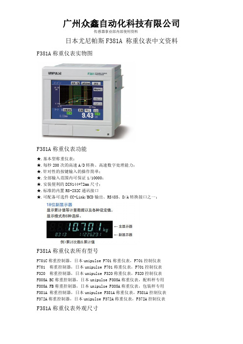
日本尤尼帕斯F381A 称重仪表中文资料F381A称重仪表实物图
F381A称重仪表功能
★.基本型称重仪表;
★.每秒200次的高速A/D转换、高速数字处理能力;
★.针对性的按键输入的操作简单;
★.全部输入范围内可保证1/10000;
★.安装便利的DIN144*72mm尺寸;
★.标准的内置RS-232C通讯接口
★.可配备可选件CC-Link/BCD输出、RS485、D/A转换接口之一;
F381A称重仪表所有型号
F701C称重控制器,日本unipulse F701称重仪表,F701控制仪表
F701 称重控制器,日本unipulse F701称重仪表,F701控制仪表
F320 称重控制器,日本unipulse F320称重仪表,F320控制仪表
F8O5A BC称重控制器,日本unipulse F8O5A称重仪表,配料秤专用
F8O5A FB称重控制器,日本unipulse F8O5A称重仪表,包装秤专用
F381A 称重控制器,日本unipulse F381A称重仪表,F381A控制仪表
F372A称重控制器,日本unipulse F372A称重仪表,F372A控制仪表
F381A称重仪表外观尺寸
F701称重仪表技术参数
F701称重仪表性能。
尤尼帕斯-F381A特点,尤尼帕斯-F381A用途,
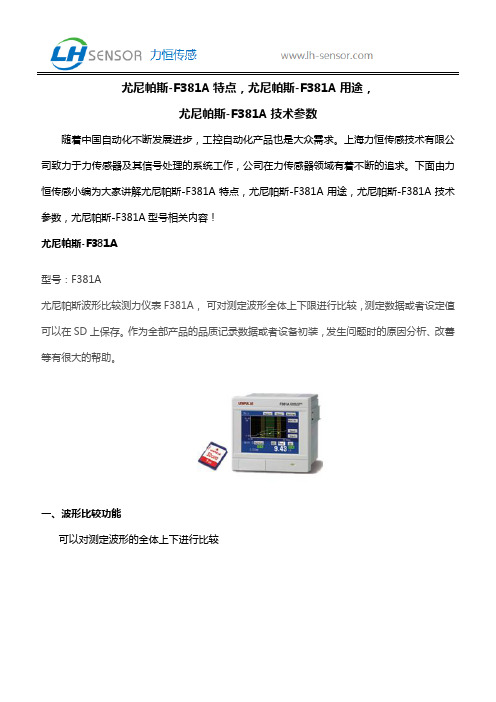
尤尼帕斯-F381A特点,尤尼帕斯-F381A用途,尤尼帕斯-F381A技术参数随着中国自动化不断发展进步,工控自动化产品也是大众需求。
上海力恒传感技术有限公司致力于力传感器及其信号处理的系统工作,公司在力传感器领域有着不断的追求。
下面由力恒传感小编为大家讲解尤尼帕斯-F381A特点,尤尼帕斯-F381A用途,尤尼帕斯-F381A技术参数,尤尼帕斯-F381A型号相关内容!尤尼帕斯-F381A型号:F381A尤尼帕斯波形比较测力仪表F381A,可对测定波形全体上下限进行比较,测定数据或者设定值可以在SD上保存。
作为全部产品的品质记录数据或者设备初装,发生问题时的原因分析、改善等有很大的帮助。
一、波形比较功能可以对测定波形的全体上下进行比较l 符合欧洲CE标准、符合RoHS环保标准l 每秒4000次的高速处理l 模拟输出:电压输出和输入信号成比例,有利于记录器做记录,荷重式输入1mV/V约等于2Vl 丰富的通讯接口:RS-232C/DeviceNet/CC-Link/Ethernetl 3.5英寸的彩色液晶&触摸式显示屏,触摸式显示屏可以直接操作使设定变得简单l 出色的操作性:不必要的设定项目自动锁定,按照设定的顺序显示项目l I/O输入:+COM/-COM 共用 I/O输出:可以选择Sink type/Source type可以连接PLC等外部设备二、测定的数值通过SD卡进行保存测定数据或者是设定值可以在SD卡上保存。
作为全部产品的品质记录数据,对设备初装、问题原因分析、改善等有很大的好处。
数据可以简单的变换成CSV文件,通过Microsoft Excel可以进行编辑三、万能保持功能可以将测定区间分割开来,任意切换保持功能(采样、峰值、谷值、P-P、平均值、极大、极小、变化点、终位移)对产品进行判断。
每个区间都可以指定上限值、下限值、保持的种类。
一个过程可以同时对复数的监测点进行测定,进而判断工件的合格与否。
美国钢铁产品的标准比较多
美国钢铁产品的标准比较多,主要有以下几种:美国钢铁产品的标准比较多,主要有以下几种:ANSI 美国国家标准AISI??美国钢铁学会标准ASTM 美国材料与试验协会标准ASME 美国机械工程师协会标准AMS 航天材料规格(美国航空工业最常用的一种材料规格,由SAE制定)API 美国石油学会标准AWS 美国焊接协会标准SAE 美国机动车工程师协会标准MIL 美国军用标准QQ 美国联邦政府标准A216::WCB , WCCA217: WC6 , WC9 , C5 (ZGCr5Mo)A351: CF8 , CF3 , CF3 M , CF8C标准号? ? ? ? 标准中文名称? ? ? ? 标准英文名称ASTM A1-00 ? ? ? ? 碳素钢丁字轨? ? ? ? Standard Specification for Carbon Steel Tee Rails ASTM A2-02 ? ? ? ? 普通型,带槽和防护型碳素工字钢轨? ? ? ? Standard Specification for Carbon Steel Girder Rails of Plain, Grooved, and Guard TypesASTM A3-01 ? ? ? ? 低、中、高碳素钢鱼尾(连接)板? ? ? ? Standard Specification for Steel Joint Bars, Low, Medium, and High Carbon (Non-Heat-Treated)ASTM A6/A6M-04a ? ? ? ? 轧制结构钢板材、型材和薄板桩通用技术要求? ? ? ? Standard Specification for General Requirements for Rolled Structural Steel Bars, Plates, Shapes, and Sheet Piling ASTM A20/A20M-04a ? ? ? ? 压力容器用钢板材通用要求? ? ? ? Standard Specification for General Requirements for Steel Plates for Pressure VesselsASTM A27/A27M-03 ? ? ? ? 通用碳素钢铸件? ? ? ? Standard Specification for Steel Castings, Carbon, for General ApplicationASTM A29/A29M-04 ? ? ? ? 热锻及冷加工碳素钢和合金钢棒? ? ? ? Standard Specification for Steel Bars, Carbon and Alloy, Hot-Wrought, General Requirements forASTM A31-04 ? ? ? ? 钢铆钉及铆钉和压力容器用棒材? ? ? ? Standard Specification for Steel Rivets and Bars for Rivets, Pressure VesselsASTM A34/A34M-01 ? ? ? ? 磁性材料的抽样和采购试验的标准惯例? ? ? ? Standard Practice for Sampling and Procurement Testing of Magnetic MaterialsASTM A36/A36M-04 ? ? ? ? 碳素结构钢技术规范? ? ? ? Standard Specification for Carbon Structural SteelASTM A47/A47M-99 ? ? ? ? 铁素体可锻铁铸件? ? ? ? Standard Specification for Ferritic Malleable Iron CastingsASTM A48/A48M-03 ? ? ? ? 灰铁铸件? ? ? ? Standard Specification for Gray Iron CastingsASTM A49-01 ? ? ? ? 经热处理的碳素钢鱼尾(连接)板,微合金鱼尾板及锻制碳素钢异型鱼尾板? ? ? ? Standard Specification for Heat-Treated Carbon Steel Joint Bars, Microalloyed Joint Bars, and Forged Carbon Steel Compromise Joint BarsASTM A53/A53M-04 ? ? ? ? 无镀层热浸的、镀锌的、焊接的及无缝钢管的技术规范? ? ? ? Standard Specification for Pipe, Steel, Black and Hot-Dipped, Zinc-Coated, Welded and SeamlessASTM A65-01 ? ? ? ? 钢轨道钉? ? ? ? Standard Specification for Steel Track SpikesASTM A66-01 ? ? ? ? 钢质螺旋道钉? ? ? ? Standard Specification for Steel Screw SpikesASTM A67-00 ? ? ? ? 热加工低碳钢和高碳钢垫板技术规范? ? ? ? Standard Specification for Steel Tie Plates, Low-Carbon and High-Carbon Hot-WorkedASTM A74-04 ? ? ? ? 铸铁污水管及配件的技术规范? ? ? ? Standard Specification for Cast Iron Soil Pipe and FittingsASTM A82-02 ? ? ? ? 钢筋混凝土用无节钢丝? ? ? ? Standard Specification for Steel Wire, Plain, for Concrete ReinforcementASTM A90/A90M-01 ? ? ? ? 镀锌和镀锌合金钢铁制品镀层重量的试验方法? ? ? ? Standard Test Method for Weight [Mass] of Coating on Iron and Steel Articles with Zinc or Zinc-Alloy Coatings ASTM A99-03 ? ? ? ? 锰铁合金? ? ? ? Standard Specification for FerromanganeseASTM A100-04 ? ? ? ? 硅铁? ? ? ? Standard Specification for FerrosiliconASTM A101-04 ? ? ? ? 铬铁? ? ? ? Standard Specification for FerrochromiumASTM A102-04 ? ? ? ? 钒铁合金? ? ? ? Standard Specification for FerrovanadiumASTM A105/A105M-03 ? ? ? ? 管系部件用碳素钢锻件? ? ? ? Standard Specification for Carbon Steel Forgings for Piping ApplicationsASTM A106/A106M-04a ? ? ? ? 高温用无缝碳素钢管? ? ? ? Standard Specification for Seamless Carbon Steel Pipe for High-Temperature ServiceASTM A108-03 ? ? ? ? 优质冷加工碳素钢棒材技术规范? ? ? ? Standard Specification for Steel Bar, Carbon and Alloy, Cold-FinishedASTM A109/A109M-03 ? ? ? ? 冷轧碳素钢带技术规范? ? ? ? Standard Specification for Steel, Strip, Carbon (0.25 Maximum Percent), Cold-RolledASTM A111-99a(2004)e1 ? ? ? ? 电话和电报线路用镀锌"铁"丝规格? ? ? ? Standard Specification for Zinc-Coated (Galvanized) Iron Telephone and Telegraph Line WireASTM A116-00 ? ? ? ? 镀锌钢丝编织栏栅网? ? ? ? Standard Specification for Metallic-Coated, Steel Woven Wire Fence FabricASTM A121-99(2004) ? ? ? ? 镀锌刺钢丝? ? ? ? Standard Specification for Mettalic-Coated Carbon Steel Barbed WireASTM A123/A123M-02 ? ? ? ? 钢铁产品的锌镀层(热浸镀锌)技术规范? ? ? ? Standard Specification for Zinc (Hot-Dip Galvanized) Coatings on Iron and Steel ProductsASTM A125-96(2001) ? ? ? ? 热处理螺旋形钢弹簧? ? ? ? Standard Specification for Steel Springs, Helical, Heat-TreatedASTM A126-04 ? ? ? ? 阀门、法兰和管配件用灰铁铸件? ? ? ? Standard Specification for Gray Iron Castings for Valves, Flanges, and Pipe FittingsASTM A128/A128M-93(2003) ? ? ? ? 钢铸件,奥氏体锰? ? ? ? Standard Specification for Steel Castings, Austenitic ManganeseASTM A131/A131M-04 ? ? ? ? 海船用结构钢? ? ? ? Standard Specification for Structural Steel for ShipsASTM A132-04 ? ? ? ? 钼铁合金? ? ? ? Standard Specification for FerromolybdenumASTM A134-96(2001) ? ? ? ? 电熔(电弧)焊钢管(NPS为16英寸和16英寸以上)? ? ? ? Standard Specification for Pipe, Steel, Electric-Fusion (Arc)-Welded (Sizes NPS 16 and Over)ASTM A135-01 ? ? ? ? 电阻焊钢管? ? ? ? Standard Specification for Electric-Resistance-Welded Steel PipeASTM A139/A139M-04 ? ? ? ? 电熔(电弧)焊钢管(4英寸以上的)? ? ? ? Standard Specification for Electric-Fusion (Arc)-Welded Steel Pipe (NPS 4 and Over)ASTM A143/A143M-03 ? ? ? ? 热浸镀锌结构钢制品防脆裂措施和探测脆裂的程序? ? ? ? Standard Practice for Safeguarding Against Embrittlement of Hot-Dip Galvanized Structural Steel Products and Procedure for Detecting EmbrittlementASTM A144-02 ? ? ? ? 铁钨合金规范? ? ? ? Specification for FerrotungstenASTM A146-04 ? ? ? ? 氧化钼制品? ? ? ? Standard Specification for Molybdenum Oxide Products ASTM A148/A148M-03 ? ? ? ? 结构用高强度钢铸件? ? ? ? Standard Specification for Steel Castings, High Strength, for Structural PurposesASTM A153/A153M-04 ? ? ? ? 钢铁制金属构件上镀锌层(热浸)? ? ? ? Standard Specification for Zinc Coating (Hot-Dip) on Iron and Steel HardwareASTM A159-83(2001) ? ? ? ? 汽车用灰铁铸件? ? ? ? Standard Specification for Automotive Gray Iron CastingsASTM A167-99 ? ? ? ? 不锈钢和耐热铬镍钢板、薄板及带材? ? ? ? Standard Specification for Stainless and Heat-Resisting Chromium-Nickel Steel Plate, Sheet, and StripASTM A176-99 ? ? ? ? 不锈钢和耐热铬钢板、薄板及带材? ? ? ? Standard Specification for Stainless and Heat-Resisting Chromium Steel Plate, Sheet, and StripASTM A178/A178M-02 ? ? ? ? 电阻焊接碳素钢钢管及碳锰钢锅炉和过热器管的技术规范? ? ? ? Standard Specification for Electric-Resistance-Welded Carbon Steel and Carbon-Manganese Steel Boiler and Superheater TubesASTM A179/A179M-90a(2001) ? ? ? ? 热交换器和冷凝器用无缝冷拉低碳钢管? ? ? ? Standard Specification for Seamless Cold-Drawn Low-Carbon Steel Heat-Exchanger and Condenser Tubes ASTM A181/A181M-01 ? ? ? ? 普通锻制碳素钢管的规格? ? ? ? Standard Specification for Carbon Steel Forgings, for General-Purpose PipingASTM A182/A182M-02 ? ? ? ? 高温设备用锻制或轧制的合金钢管法兰、锻制管件、阀门及零件? ? ? ? Standard Specification for Forged or Rolled Alloy-Steel Pipe Flanges, Forged Fittings, and Valves and Parts for High-Temperature ServiceASTM A183-03 ? ? ? ? 钢轨用碳素钢螺栓和螺母? ? ? ? Standard Specification for Carbon Steel Track Bolts and NutsASTM A184/A184M-01 ? ? ? ? 混凝土加筋用变形钢筋编织网? ? ? ? Standard Specification for Fabricated Deformed Steel Bar Mats for Concrete ReinforcementASTM A185-02 ? ? ? ? 钢筋混凝土用焊接钢丝结构? ? ? ? Standard Specification for Steel Welded Wire Reinforcement, Plain, for ConcreteASTM A192/A192M-02 ? ? ? ? 高压用无缝碳素钢锅炉管? ? ? ? Standard Specification for Seamless Carbon Steel Boiler Tubes for High-Pressure ServiceASTM A193/A193M-04b ? ? ? ? 高温设备用合金钢和不锈钢螺栓材料? ? ? ? Standard Specification for Alloy-Steel and Stainless Steel Bolting Materials for High-Temperature ServiceASTM A194/A194M-04a ? ? ? ? 高温和高压设备用碳素钢与合金钢螺栓和螺母的规格? ? ? ? Standard Specification for Carbon and Alloy Steel Nuts for Bolts for High Pressure or High Temperature Service, or BothASTM A197/A197M-00 ? ? ? ? 化铁炉用可锻铸铁? ? ? ? Standard Specification for Cupola Malleable IronASTM A202/A202M-03 ? ? ? ? 压力容器用铬锰硅合金钢板? ? ? ? Standard Specification for Pressure Vessel Plates, Alloy Steel, Chromium-Manganese-SiliconASTM A203/A203M-97(2003) ? ? ? ? 压力容器用镍合金钢板? ? ? ? Standard Specification for Pressure Vessel Plates, Alloy Steel, NickelASTM A204/A204M-03 ? ? ? ? 压力容器用钼合金钢板? ? ? ? Standard Specification for Pressure Vessel Plates, Alloy Steel, MolybdenumASTM A209/A209M-03 ? ? ? ? 锅炉和过热器用无缝碳钼合金钢管? ? ? ? Standard Specification for Seamless Carbon-Molybdenum Alloy-Steel Boiler and Superheater TubesASTM A210/A210M-02 ? ? ? ? 锅炉和过热器用无缝中碳素管? ? ? ? Standard Specification for Seamless Medium-Carbon Steel Boiler and Superheater TubesASTM A213/A213M-04 ? ? ? ? 无缝铁素体和奥氏体合金钢锅炉、过热器和换热器管? ? ? ? Standard Specification for Seamless Ferritic and Austenitic Alloy-Steel Boiler, Superheater, andHeat-Exchanger TubesASTM A214/A214M-96(2001) ? ? ? ? 热交换器与冷凝器用电阻焊接碳素钢管? ? ? ? Standard Specification for Electric-Resistance-Welded Carbon Steel Heat-Exchanger and Condenser Tubes ASTM A216/A216M-93(2003) ? ? ? ? 高温下使用的适合于熔焊的碳素钢铸件规格? ? ? ? Standard Specification for Steel Castings, Carbon, Suitable for Fusion Welding, for High- Temperature ServiceASTM A217/A217M-02 ? ? ? ? 适合高温受压零件用合金钢和马氏体不锈钢铸件? ? ? ? Standard Specification for Steel Castings, Martensitic Stainless and Alloy, for Pressure-Containing Parts, Suitable for High-Temperature ServiceASTM A220/A220M-99 ? ? ? ? 珠光体可锻铁? ? ? ? Standard Specification for Pearlitic Malleable IronASTM A225/A225M-03 ? ? ? ? 压力容器用锰矾镍合金钢板? ? ? ? Standard Specification for Pressure Vessel Plates, Alloy Steel, Manganese-Vanadium-NickelASTM A227/A227M-99 ? ? ? ? 机械弹簧用冷拉钢丝? ? ? ? Standard Specification for Steel Wire, Cold-Drawn for Mechanical SpringsASTM A228/A228M-02 ? ? ? ? 乐器用优质弹簧钢丝? ? ? ? Standard Specification for Steel Wire, Music Spring QualityASTM A229/A229M-99 ? ? ? ? 机械弹簧用油回火的钢丝? ? ? ? Standard Specification for Steel Wire, Oil-Tempered for Mechanical SpringsASTM A230/A230M-99 ? ? ? ? 阀门用油回火优质碳素钢弹簧丝? ? ? ? Standard Specification for Steel Wire, Oil-Tempered Carbon Valve Spring QualityASTM A231/A231M-96(2002) ? ? ? ? 铬钒合金钢弹簧丝? ? ? ? Standard Specification for Chromium-Vanadium Alloy Steel Spring WireASTM A232/A232M-99 ? ? ? ? 阀门用优质铬钒合金钢弹簧丝? ? ? ? Standard Specification for Chromium-Vanadium Alloy Steel Valve Spring Quality WireASTM A234/A234M-04 ? ? ? ? 中温与高温下使用的锻制碳素钢及合金钢管配件? ? ? ? Standard Specification for Piping Fittings of Wrought Carbon Steel and Alloy Steel for Moderate and High Temperature ServiceASTM A239-95(2004) ? ? ? ? 用普力斯试验法(硫酸铜浸蚀)确定铁或钢制品上镀锌层最薄点的测试方法? ? ? ? Standard Practice for Locating the Thinnest Spot in a Zinc (Galvanized) Coating on Iron or Steel ArticlesASTM A240/A240M-04ae1 ? ? ? ? 压力容器用耐热铬及铬镍不锈钢板、薄板及带材? ? ? ? Standard Specification for Chromium and Chromium-Nickel Stainless Steel Plate, Sheet, and Strip for Pressure Vessels and for General ApplicationsASTM A242/A242M-04 ? ? ? ? 高强度低合金结构钢? ? ? ? Standard Specification for High-Strength Low-Alloy Structural SteelASTM A247-67(1998) ? ? ? ? 铁铸件中石墨显微结构评定试验方法? ? ? ? Standard Test Method for Evaluating the Microstructure of Graphite in Iron CastingsASTM A249/A249M-04 ? ? ? ? 锅炉、过热器、换热器和冷凝器用焊接奥氏体钢管? ? ? ? Standard Specification for Welded Austenitic Steel Boiler, Superheater, Heat-Exchanger, and Condenser TubesASTM A250/A250M-04 ? ? ? ? 锅炉和过热器用电阻焊铁素体合金钢管? ? ? ? Standard Specification for Electric-Resistance-Welded Ferritic Alloy-Steel Boiler and Superheater TubesASTM A252-98(2002) ? ? ? ? 焊接钢和无缝钢管桩? ? ? ? Standard Specification for Welded and Seamless Steel Pipe PilesASTM A254-97(2002) ? ? ? ? 铜焊钢管规格? ? ? ? Standard Specification for Copper-Brazed Steel TubingASTM A255-02 ? ? ? ? 测定钢淬透性用末端淬火试验的标准试验方法? ? ? ? Standard Test Method for Determining Hardenability of SteelASTM A262-03 ? ? ? ? 奥氏体不锈钢晶间浸蚀敏感性的检测? ? ? ? Standard Practices for Detecting Susceptibility to Intergranular Attack in Austenitic Stainless SteelsASTM A263-03 ? ? ? ? 耐腐蚀铬钢包覆板材,薄板材及带材技术规范? ? ? ? Standard Specification for Stainless Chromium Steel-Clad PlateASTM A264-03 ? ? ? ? 包覆的不锈铬镍钢板,薄板及带材规格? ? ? ? Specification for Stainless Chromium-Nickel Steel-Clad PlateASTM A265-03 ? ? ? ? 镍和镍基合金包覆钢板规格? ? ? ? Standard Specification for Nickel and Nickel-Base Alloy-Clad Steel PlateASTM A266/A266M-03a ? ? ? ? 压力容器部件用碳素钢锻件规格? ? ? ? Standard Specification for Carbon Steel Forgings for Pressure Vessel ComponentsASTM A268/A268M-04 ? ? ? ? 一般设备用无缝和焊接铁素体与马氏体不锈钢管? ? ? ? Standard Specification for Seamless and Welded Ferritic and Martensitic Stainless Steel Tubing for General ServiceASTM A269-04 ? ? ? ? 一般设备用无缝和焊接奥氏体不锈钢管? ? ? ? Standard Specification for Seamless and Welded Austenitic Stainless Steel Tubing for General ServiceASTM A270-03a ? ? ? ? 卫生设施用无缝钢和焊接奥氏体不锈钢管? ? ? ? Standard Specification for Seamless and Welded Austenitic Stainless Steel Sanitary TubingASTM A275/A275M-98(2003) ? ? ? ? 钢锻件的磁粉检查试验方法? ? ? ? Standard Test Method for Magnetic Particle Examination of Steel ForgingsASTM A276-04 ? ? ? ? 不锈钢棒材和型材? ? ? ? Standard Specification for Stainless Steel Bars and ShapesASTM A278/A278M-01 ? ? ? ? 适用于650F容压部件用灰铸铁件的技术规范? ? ? ? Standard Specification for Gray Iron Castings for Pressure-Containing Parts for Temperatures Up to 650°F (350°C) ASTM A283/A283M-03 ? ? ? ? 低和中等抗拉强度碳素钢板? ? ? ? Standard Specification for Low and Intermediate Tensile Strength Carbon Steel PlatesASTM A285/A285M-03 ? ? ? ? 压力容器用低和中等抗拉强度的碳素钢板? ? ? ? Standard Specification for Pressure Vessel Plates, Carbon Steel, Low- and Intermediate-Tensile StrengthASTM A288-91(2003) ? ? ? ? 涡轮发电机磁性定位环用碳素钢和合金钢锻件? ? ? ? Standard Specification for Carbon and Alloy Steel Forgings for Magnetic Retaining Rings for Turbine Generators标准号? ? ? ? 标准中文名称? ? ? ? 标准英文名称ASTM A289/A289M-97(2003) ? ? ? ? 发电机非磁性定位环用合金钢锻件的技术规范? ? ? ? Standard Specification for Alloy Steel Forgings for Nonmagnetic Retaining Rings for GeneratorsASTM A290-02 ? ? ? ? 减速器环用碳素钢和合金钢锻件? ? ? ? Standard Specification for Carbon and Alloy Steel Forgings for Rings for Reduction GearsASTM A291-03 ? ? ? ? 减速器小齿轮、齿轮和心轴用碳素钢和合金钢锻件? ? ? ? Standard Specification for Steel Forgings, Carbon and Alloy, for Pinions, Gears and Shafts for Reduction Gears ASTM A295-98 ? ? ? ? 高碳耐磨轴承钢技术规范? ? ? ? Standard Specification for High-Carbon Anti-Friction Bearing SteelASTM A297/A297M-97(2003) ? ? ? ? 一般用耐热铬铁与镍铬铁合金钢铸件规格? ? ? ? Standard Specification for Steel Castings, Iron-Chromium and Iron-Chromium-Nickel, Heat Resistant, for General ApplicationASTM A299/A299M-04 ? ? ? ? 压力容器用锰硅碳钢板? ? ? ? Standard Specification for Pressure Vessel Plates, Carbon Steel, Manganese-SiliconASTM A302/A302M-03 ? ? ? ? 压力容器用锰钼和锰钼镍合金钢板? ? ? ? Standard Specification for Pressure Vessel Plates, Alloy Steel, Manganese-Molybdenum and Manganese-Molybdenum-Nickel ASTM A304-04 ? ? ? ? 有末端淬火淬透性要求的合金钢棒材的技术规范? ? ? ? Standard Specification for Carbon and Alloy Steel Bars Subject to End-Quench Hardenability RequirementsASTM A307-04 ? ? ? ? 抗拉强度为60000psi的碳素钢螺栓和螺柱的技术规范? ? ? ? Standard Specification for Carbon Steel Bolts and Studs, 60 000 PSI Tensile StrengthASTM A308/A308M-03 ? ? ? ? 经热浸处理镀有铅锡合金的薄板材的技术规范? ? ? ? Standard Specification for Steel Sheet, Terne (Lead-Tin Alloy) Coated by the Hot-Dip ProcessASTM A309-01 ? ? ? ? 用三点试验法测定长镀锌薄钢板镀层的重量成分的试验方法? ? ? ? Standard Test Method for Weight and Composition of Coating on Terne Sheet by the Triple-Spot TestASTM A311/A311M-04 ? ? ? ? 有机械性能要求的消除应力的冷拉碳素钢棒? ? ? ? Standard Specification for Cold-Drawn, Stress-Relieved Carbon Steel Bars Subject to Mechanical Property Requirements ASTM A312/A312M-04a ? ? ? ? 无缝和焊接奥氏体不锈钢管? ? ? ? Standard Specification for Seamless, Welded, and Heavily Cold Worked Austenitic Stainless Steel PipesASTM A313/A313M-03 ? ? ? ? 不锈钢弹簧丝技术规范? ? ? ? Standard Specification for Stainless Steel Spring WireASTM A314-97(2002) ? ? ? ? 锻造用不锈及耐热钢坯及钢棒规格? ? ? ? Standard Specification for Stainless Steel Billets and Bars for ForgingASTM A319-71(2001) ? ? ? ? 高温无压部件用灰铁铸件? ? ? ? Standard Specification for Gray Iron Castings for Elevated Temperatures for Non-Pressure Containing PartsASTM A320/A320M-04 ? ? ? ? 低温用合金钢螺栓材料规格? ? ? ? Standard Specification for Alloy-Steel and Stainless Steel Bolting Materials for Low-Temperature ServiceASTM A321-90(2001) ? ? ? ? 经淬火和回火的碳素钢棒? ? ? ? Standard Specification for Steel Bars, Carbon, Quenched and TemperedASTM A322-91(2001)e1 ? ? ? ? 合金钢棒材.级别? ? ? ? Standard Specification for Steel Bars, Alloy, Standard GradesASTM A323-93(2000) ? ? ? ? 硼铁规格? ? ? ? Standard Specification for FerroboronASTM A324-73(2000) ? ? ? ? 钛铁合金? ? ? ? Standard Specification for FerrotitaniumASTM A325-04a ? ? ? ? 经热处理最小抗拉强度为120/105ksi的热处理钢结构螺栓? ? ? ? Standard Specification for Structural Bolts, Steel, Heat Treated, 120/105 ksi Minimum Tensile Strength ASTM A325M-04a ? ? ? ? 经热处理最小抗拉强度为830Mpa的热处理钢结构螺栓? ? ? ? Standard Specification for Structural Bolts, Steel, Heat Treated 830 Mpa Minimum Tensile Strength [Metric] ASTM A327-91(1997) ? ? ? ? 铸铁冲击试验方法? ? ? ? Standard Test Methods for Impact Testing of Cast IronsASTM A327M-91(1997) ? ? ? ? 铸铁冲击试验方法(米制)? ? ? ? Standard Test Methods for Impact Testing of Cast Irons (Metric)ASTM A328/A328M-03 ? ? ? ? 薄钢板桩? ? ? ? Standard Specification for Steel Sheet Piling ASTM A333/A333M-04a ? ? ? ? 低温用无缝与焊接钢管规格? ? ? ? Standard Specification for Seamless and Welded Steel Pipe for Low-Temperature ServiceASTM A334/A334M-04a ? ? ? ? 低温设备用无缝与焊接碳素和合金钢管? ? ? ? Standard Specification for Seamless and Welded Carbon and Alloy-Steel Tubes for Low-Temperature ServiceASTM A335/A335M-03 ? ? ? ? 高温用无缝铁素体合金钢管? ? ? ? Standard Specification for Seamless Ferritic Alloy-Steel Pipe for High-Temperature ServiceASTM A336/A336M-03a ? ? ? ? 压力与高温部件用合金钢锻件规格? ? ? ? Standard Specification for Alloy Steel Forgings for Pressure and High-Temperature PartsASTM A338-84(2004) ? ? ? ? 铁路,船舶和其他重型装备在温度达到650华氏度(345摄氏度)时使用的可锻铸铁法兰,管件和阀门零件? ? ? ? Standard Specification for Malleable Iron Flanges, Pipe Fittings, and Valve Parts for Railroad, Marine, and Other Heavy Duty Service at Temperatures Up to 650°F (345°C)ASTM A340-03a ? ? ? ? 有关磁性试验用符号和定义的术语? ? ? ? Standard Terminology of Symbols and Definitions Relating to Magnetic TestingASTM A341/A341M-00 ? ? ? ? 用直流磁导计和冲击试验法测定材料的直流磁性能的试验方法? ? ? ? Standard Test Method for Direct Current Magnetic Properties of Materials Using D-C Permeameters and the Ballistic Test MethodsASTM A342/A342M-99 ? ? ? ? 磁铁材料导磁率的试验方法? ? ? ? Standard Test Methods for Permeability of Feebly Magnetic MaterialsASTM A343/A343M-03 ? ? ? ? 在电力频率下用瓦特计-安培计-伏特计法(100-1000赫兹)和25 厘米艾普斯亭(EPSTEIN) 机架测定材料的交流电磁性能的试验方法? ? ? ? Standard Test Method forAlternating-Current Magnetic Properties of Materials at Power Frequencies UsingWattmeter-Ammeter-Voltmeter Method and 25-cm Epstein Test FrameASTM A345-98 ? ? ? ? 磁设备用平轧电炉钢? ? ? ? Standard Specification for Flat-Rolled Electrical Steels for Magnetic ApplicationsASTM A348/A348M-00 ? ? ? ? 用瓦特计--安培计--伏特计法(100-10000赫兹)和25厘米艾普斯亭框测定材料的交流磁性能的试验方法? ? ? ? Standard Test Method for Alternating Current Magnetic Properties of Materials Using the Wattmeter-Ammeter-Voltmeter Method, 100 to 10 000 Hz and 25-cm Epstein FrameASTM A350/A350M-04 ? ? ? ? 要求进行缺口韧性试验的管道部件用碳素钢与低合金钢锻件技术规范? ? ? ? Standard Specification for Carbon and Low-Alloy Steel Forgings, Requiring Notch Toughness Testing for Piping ComponentsASTM A351/A351M-03 ? ? ? ? 容压零件用奥氏体及奥氏体铁素体铸铁的技术规范? ? ? ? Standard Specification for Castings, Austenitic, Austenitic-Ferritic (Duplex), for Pressure-Containing PartsASTM A352/A352M-03 ? ? ? ? 低温受压零件用铁素体和马氏体钢铸件规格? ? ? ? Standard Specification for Steel Castings, Ferritic and Martensitic, for Pressure-Containing Parts, Suitable for Low-Temperature ServiceASTM A353/A353M-93(1999) ? ? ? ? 压力容器用经二次正火及回火处理的含9%镍的合金钢板? ? ? ? Standard Specification for Pressure Vessel Plates, Alloy Steel, 9 Percent Nickel,Double-Normalized and TemperedASTM A354-04 ? ? ? ? 淬火与回火合金钢螺栓,双头螺栓及其他外螺纹紧固件规格? ? ? ? Standard Specification for Quenched and Tempered Alloy Steel Bolts, Studs, and Other Externally Threaded FastenersASTM A355-89(2000) ? ? ? ? 渗氮用合金钢棒? ? ? ? Standard Specification for Steel Bars, Alloys, for NitridingASTM A356/A356M-98(2003) ? ? ? ? 蒸汽轮机用厚壁碳素钢、低合金钢和不锈钢铸件? ? ? ? Standard Specification for Steel Castings, Carbon, Low Alloy, and Stainless Steel, Heavy-Walled for Steam TurbinesASTM A358/A358M-04 ? ? ? ? 高温用电熔焊奥氏体铬镍合金钢管? ? ? ? Standard Specification for Electric-Fusion-Welded Austenitic Chromium-Nickel Stainless Steel Pipe for High-Temperature Service and General ApplicationsASTM A363-03 ? ? ? ? 地面架空线用镀锌钢丝绳? ? ? ? Standard Specification for Zinc-Coated (Galvanized) Steel Overhead Ground Wire StrandASTM A367-60(1999) ? ? ? ? 铸铁的激冷试验方法? ? ? ? Standard Test Methods of Chill Testing of Cast IronASTM A368-95a(2000) ? ? ? ? 不锈钢和耐热钢丝绳的标准? ? ? ? Standard Specification for Stainless Steel Wire StrandASTM A369/A369M-02 ? ? ? ? 高温用锻制和镗孔碳素钢管和铁素体合金钢管? ? ? ? Standard Specification for Carbon and Ferritic Alloy Steel Forged and Bored Pipe for High-Temperature ServiceASTM A370-03a ? ? ? ? 钢制品机械测试的标准试验方法和定义? ? ? ? Standard Test Methods and Definitions for Mechanical Testing of Steel Products标准号? ? ? ? 标准中文名称? ? ? ? 标准英文名称ASTM A372/A372M-03 ? ? ? ? 薄壁压力容器用碳素钢及合金钢锻件? ? ? ? Standard Specification for Carbon and Alloy Steel Forgings for Thin-Walled Pressure VesselsASTM A376/A376M-02a ? ? ? ? 高温中心站用无缝奥氏钢管? ? ? ? Standard Specification for Seamless Austenitic Steel Pipe for High-Temperature Central-Station ServiceASTM A377-03 ? ? ? ? 球墨铸铁压力管规范索引? ? ? ? Standard Index of Specifications for Ductile-Iron Pressure PipeASTM A380-99e1 ? ? ? ? 不锈钢零件、设备和系统的清洗和除垢? ? ? ? Standard Practice for Cleaning, Descaling, and Passivation of Stainless Steel Parts, Equipment, and SystemsASTM A381-96(2001) ? ? ? ? 高压输送用金属弧焊钢管? ? ? ? Standard Specification forMetal-Arc-Welded Steel Pipe for Use With High-Pressure Transmission SystemsASTM A384/A384M-02 ? ? ? ? 防止钢组件热浸镀锌时翘曲和扭曲用安全保护? ? ? ? Standard Practice for Safeguarding Against Warpage and Distortion During Hot-Dip Galvanizing of Steel Assemblies ASTM A385-03 ? ? ? ? 提供高质量镀锌覆层(热浸)? ? ? ? Standard Practice for Providing High-Quality Zinc Coatings (Hot-Dip)ASTM A387/A387M-03 ? ? ? ? 压力容器用铬钼合金钢板? ? ? ? Standard Specification for Pressure Vessel Plates, Alloy Steel, Chromium-MolybdenumASTM A388/A388M-03 ? ? ? ? 重型钢锻件超声波检测? ? ? ? Standard Practice for Ultrasonic Examination of Heavy Steel ForgingsASTM A389/A389M-03 ? ? ? ? 适合高温受压部件用经特殊热处理的合金钢铸件规格? ? ? ? Standard Specification for Steel Castings, Alloy, Specially Heat-Treated, for Pressure-Containing Parts, Suitable for High-Temperature ServiceASTM A390-95(2001) ? ? ? ? 饲养家禽用镀锌钢丝栏栅网(六角形和直线形)? ? ? ? Standard Specification for Zinc-Coated (Galvanized) Steel Poultry Fence Fabric (Hexagonal and Straight Line)ASTM A391/A391M-01 ? ? ? ? 80号合金钢链条? ? ? ? Standard Specification for Grade 80 Alloy Steel ChainASTM A392-03 ? ? ? ? 镀锌钢丝链环栏栅网? ? ? ? Standard Specification for Zinc-Coated Steel Chain-Link Fence FabricASTM A394-04 ? ? ? ? 传动塔架用镀锌和裸露钢螺栓? ? ? ? Standard Specification for Steel Transmission Tower Bolts, Zinc-Coated and BareASTM A395/A395M-99e1 ? ? ? ? 高温用铁素体球墨铸铁受压铸件? ? ? ? Standard Specification for Ferritic Ductile Iron Pressure-Retaining Castings for Use at Elevated TemperaturesASTM A400-69(2000) ? ? ? ? 钢棒的成分及机械性能选择指南? ? ? ? Standard Practice for Steel Bars, Selection Guide, Composition, and Mechanical PropertiesASTM A401/A401M-03 ? ? ? ? 铬硅合金钢丝? ? ? ? Standard Specification for Steel Wire, Chromium-Silicon AlloyASTM A403/A403M-04 ? ? ? ? 锻制奥氏体不锈钢管配件? ? ? ? Standard Specification for Wrought Austenitic Stainless Steel Piping FittingsASTM A407-93(2004) ? ? ? ? 盘簧用冷拉钢丝? ? ? ? Standard Specification for Steel Wire, Cold-Drawn, for Coiled-Type SpringsASTM A409/A409M-01 ? ? ? ? 腐蚀场所或高温下使用的焊接大口径奥氏体钢管? ? ? ? Standard Specification for Welded Large Diameter Austenitic Steel Pipe for Corrosive or High-Temperature ServiceASTM A411-03 ? ? ? ? 镀锌低碳钢铠装线? ? ? ? Standard Specification for Zinc-Coated (Galvanized) Low-Carbon Steel Armor WireASTM A413/A413M-01 ? ? ? ? 碳素钢链? ? ? ? Standard Specification for Carbon Steel Chain ASTM A414/A414M-04 ? ? ? ? 压力容器用碳素薄钢板? ? ? ? Standard Specification for Steel, Sheet, Carbon, for Pressure VesselsASTM A416/A416M-02 ? ? ? ? 预应力混凝土用无涂层七股钢铰线? ? ? ? Standard Specification for Steel Strand, Uncoated Seven-Wire for Prestressed ConcreteASTM A417-93(2004) ? ? ? ? 之字形、方形、正弦形家具用弹簧元件用冷拔钢丝? ? ? ? Standard Specification for Steel Wire, Cold-Drawn, for Zig-Zag, Square-Formed, and Sinuous-Type Upholstery Spring UnitsASTM A418-99(2003) ? ? ? ? 涡轮机及发电机钢转子锻件的超声波检查方法? ? ? ? Standard Test Method for Ultrasonic Examination of Turbine and Generator Steel Rotor ForgingsASTM A420/A420M-04 ? ? ? ? 低温下用锻制碳素钢和合金钢管配件? ? ? ? Standard Specification for Piping Fittings of Wrought Carbon Steel and Alloy Steel for Low-Temperature ServiceASTM A421/A421M-02 ? ? ? ? 预应力混凝土用无涂层消除应力钢丝的技术规范? ? ? ? Standard Specification for Uncoated Stress-Relieved Steel Wire for Prestressed ConcreteASTM A423/A423M-95(2000) ? ? ? ? 无缝和电焊低合金钢管? ? ? ? Standard Specification for Seamless and Electric-Welded Low-Alloy Steel TubesASTM A424-00 ? ? ? ? 搪瓷用钢薄板? ? ? ? Standard Specification for Steel, Sheet, for Porcelain EnamelingASTM A426/A426M-02 ? ? ? ? 高温用离心铸造的铁素体合金钢管? ? ? ? Standard Specification for Centrifugally Cast Ferritic Alloy Steel Pipe for High-Temperature ServiceASTM A427-02 ? ? ? ? 冷轧和热轧用锻制合金钢辊? ? ? ? Standard Specification for Wrought Alloy Steel Rolls for Cold and Hot ReductionASTM A428/A428M-01 ? ? ? ? 钢铁制品上铝覆层重量的测试方法? ? ? ? Standard Test Method for Weight [Mass] of Coating on Aluminum-Coated Iron or Steel ArticlesASTM A434-04 ? ? ? ? 热轧与冷精轧经回火及淬火的合金钢棒? ? ? ? Standard Specification for Steel Bars, Alloy, Hot-Wrought or Cold-Finished, Quenched and TemperedASTM A435/A435M-90(2001) ? ? ? ? 钢板的直射束纵向超声波检验? ? ? ? Standard Specification for Straight-Beam Ultrasonic Examination of Steel PlatesASTM A436-84(2001) ? ? ? ? 奥氏体灰口铁铸件? ? ? ? Standard Specification for Austenitic Gray Iron CastingsASTM A437/A437M-01a ? ? ? ? 高温用经特殊处理的涡轮型合金钢螺栓材料? ? ? ? Standard Specification for Alloy-Steel Turbine-Type Bolting Material Specially Heat Treated for High-Temperature ServiceASTM A439-83(1999) ? ? ? ? 奥氏体可锻铸铁铸件? ? ? ? Standard Specification for Austenitic Ductile Iron CastingsASTM A447/A447M-93(2003) ? ? ? ? 高温用镍铬铁合金钢铸件(25-12级)? ? ? ? Standard Specification for Steel Castings, Chromium-Nickel-Iron Alloy (25-12 Class), for High-Temperature Service ASTM A449-04a ? ? ? ? 经淬火和回火的钢螺栓和螺柱? ? ? ? Standard Specification for Quenched and Tempered Steel Bolts and StudsASTM A450/A450M-04 ? ? ? ? 碳素钢管、铁素体合金钢管及奥氏体合金钢管? ? ? ? Standard Specification for General Requirements for Carbon, Ferritic Alloy, and Austenitic Alloy Steel TubesASTM A451/A451M-02 ? ? ? ? 高温用离心铸造的奥氏体钢管? ? ? ? Standard Specification for Centrifugally Cast Austenitic Steel Pipe for High-Temperature ServiceASTM A453/A453M-03 ? ? ? ? 具有同奥氏体钢相类似的膨胀系数、屈服强度为50-120Ksi(345-827MPa)的耐高温螺栓材料? ? ? ? Standard Specification for High-Temperature Bolting Materials, with Expansion Coefficients Comparable to Austenitic Stainless SteelsASTM A455/A455M-03 ? ? ? ? 压力容器用高强度碳锰钢板? ? ? ? Standard Specification for Pressure Vessel Plates, Carbon Steel, High-Strength ManganeseASTM A456/A456M-99(2003) ? ? ? ? 大型曲轴锻件的磁粉检查? ? ? ? Standard Specification for Magnetic Particle Examination of Large Crankshaft ForgingsASTM A459-97(2003) ? ? ? ? 镀锌平轧扁钢铠装带? ? ? ? Standard Specification for Zinc-Coated Flat Steel Armoring TapeASTM A460-94(2004)e1 ? ? ? ? 包铜钢丝绳标准? ? ? ? Standard Specification for Copper-Clad Steel Wire StrandASTM A463/A463M-02a ? ? ? ? 热浸镀铝薄钢板? ? ? ? Standard Specification for Steel Sheet, Aluminum-Coated, by the Hot-Dip ProcessASTM A466/A466M-01 ? ? ? ? 非焊接碳素钢链? ? ? ? Standard Specification for Weldless Chain ASTM A467/A467M-01 ? ? ? ? 机器链和盘旋链? ? ? ? Standard Specification for Machine and Coil Chain标准号? ? ? ? 标准中文名称? ? ? ? 标准英文名称。
ISA-381GX-MP变压器保护测控装置技术使用说明书V1.00-161215

本说明适用于 ISA-381GA/B-MP-V1.00 及以上版本软件。 本装置用户权限密码:800。 装置型号说明:
装置型号 ISA-381GX-MP-V1.00-XXXXXX-XXXX
⑥程序校验码 ⑤基础软件生成日期 ④基础软件版本 ③MP表示66kV及以下保护测控一体化装置 ②保护系列代码 ①硬件平台代码
长园深瑞继保自动化有限公司
-I-
目录
6
数据及记录 .................................................................................................. 21
6.1 6.2 保护动作事件类型定义 .......................................................................................... 21 保护告警类型定义 .................................................................................................. 22
本说明书由长园深瑞继保自动化有限公司编写并发布,并具有对相关产品的最终解释权。 相关产品的后续升级可能会和本说明书有少许出入,说明书的升级也可能无法及时告知阁下,对此 我们表示抱歉!请注意核对实际产品与说明书的版本是否相符。 更多产品信息,请访问互联网:
欢迎拨打免费客户服务电话:400-678-8099
ห้องสมุดไป่ตู้
7
装置端子接线 .............................................................................................. 23
HSMP-3816资料
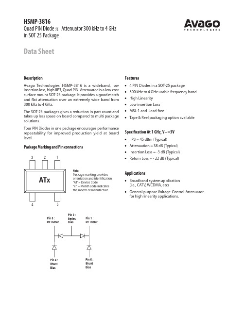
HSMP-3816Quad PIN Diode π Attenuator 300 kHz to 4 GHz in SOT 25 PackageData SheetNote:Package marking provides orientation and identification “AT”= Device Code“x” = Month code indicates the month of manufacture1ATx2345Pin 2 :Series BiasPin 3 :RF In/Out Pin 1 :RF In/OutPin 4 :Shunt Bias Pin 5 :ShuntBiasDescriptionAvago Technologies’ HSMP-3816 is a wideband, low insertion loss, high IIP3, Quad PIN Attenuator in a low cost surface mount SOT-25 package. It provides a good match and flat attenuation over an extremely wide band from 300 kHz to 4 GHz.The SOT-25 packages gives a reduction in part count and takes up less space on board compared to multi package solutions.Four PIN Diodes in one package encourages performance repeatability for improved production yield at board level.Package Marking and Pin connectionsFeatures• 4 PIN Diodes in a SOT-25 package • 300 kHz to 4 GHz usable frequency band • High Linearity • Low insertion Loss • MSL-1 and Lead-free• Tape & Reel packaging option availableSpecification At 1 GHz, V+=5V• IIP3 = 45 dBm (Typical)• Attenuation = 38 dB (Typical)• Insertion Loss = -3 dB (Typical)• Return Loss = - 22 dB (Typical)Applications• Broadband system application (i.e., CATV, WCDMA, etc)• General purpose Voltage-Control-Attenuator for high linearity applications.SymbolParameterUnitAbs MaxI f Forward Current (1 µs Pulse)Amp 1P IV Peak Inverse Voltage V 100T j Junction Temperature °C 150T stg Storage Temperature °C -60 to 150q lb Thermal Resistance [2]°C/W 167P InInput Power [3]W1.0Notes:1. Operation in excess of any one of these conditions may result in permanent damage to the device.2. Thermal Resistance is measured from junction to board using IR method.3. The Max Input Power is tested using demoboard as shown in Figure 1 at the worst-case (highest attenuation) bias condition of V+=5V, Vc=0V.Carrier Lifetime t (ns)Reverse Recovery Time T rr (ns)Total Capacitance C T (pF)15003000.27TestConditionI F = 50mA I R = 250 mAV R = 10 V I F = 20 mA 90% RecoveryV R = 50V f = 1MHzTypical Performance for HSMP-3816 Quad PIN Diode π Attenuator @ +25o CParameterTest ConditionUnitsTypicalInsertion Loss Vc = 15V, V+ = 5V, Freq = 1GHz dB -3.0Return Loss Vc = 0V, V+ = 5V, Freq = 1GHz dB -22Attenuation Vc = 0V, V+ = 5V, Freq = 1GHz dB 38Input IP3Vc = 1.5V, V+ = 5V, Freq = 1GHz dBm 45Input IP3Vc = 15V, V+ = 5V, Freq = 1GHz dBm 42Input IP3Vc = 1.5V, V+ = 5V, Freq = 100MHz dBm 37Input IP3Vc = 15V, V+ = 5V, Freq = 100MHz dBm 37Input IP3Vc = 1.5V, V+ = 5V, Freq = 30MHz dBm 35Input IP3Vc = 15V, V+ = 5V, Freq = 30MHzdBm35Notes :1. Measurement above obtained using Wideband RF circuit design shown in Figure 1 & 2Typical Performance, Tc = +25o C (Each Diode)Absolute Max Ratings [1], Tc = +25o CElectrical Specifications, Tc = +25o C (Each Diode)Minimum Breakdown Voltage V BR (V)Maximum TotalCapacitance C T (pF)Minimum Resistance at I F = 0.01mA,R H (Ω)Maximum Resistance at I F = 20mA,R L (Ω)Maximum Resistance at I F = 100mA, R T (Ω)Resistance at I F = 1mA,R M (Ω)1000.35150010 3.045 to 80TestConditionsV R = V BR Measure I R ≤ 10uAV R = 50V f = 1MHzI F = 0.01mA f = 100MHzI F = 20mA f = 100MHzI F = 100mA f = 100MHzI F = 1mA f = 100MHzNote : Rs parameters are tested under AQL 1.0VcVia Hole to GNDVia Hole to GNDto GNDV+C1C3C2R3R1C4R4R4R5C5ATxR2ComponentValueR1,R2560 Ohm R3330 Ohm R41500 Ohm R5680 Ohm C1-C547000 pFFigure 1. Wideband Quad PIN Diode π Attenuator Circuit Figure 2. Circuit Board LayoutTypical Performance Curves for Single Diode@ Tc = +25oC,0.10 1.0010.00IF - Forward Bias Current (mA)R F R e s i s t a n c e (O H M S )0.010.101.0010.00100.0000.20.40.60.81 1.2VF- Forward Voltage (V)I F - F o r w a r d C u r r e n t (m A )+125°C+25°C- 50°C0.150.200.250.300.350.400.450.500.550.6048121620Reverse Voltage (V)T o t a l C a p a c i t a n c e (p F )F=1 MHz F=10 MHzFigure 3. RF Resistance vs. Forward Bias CurrentFigure 4. Forward Current vs. Forward VoltageFigure 5. RF Capacitance vs Reverse BiasTypical Performance Curves for HSMP-3816, @ V+ = 5V, Tc = +25o CNote:1. Measurements above were obtained using Wideband RF circuit design shown in Figures 1 and2.2. Typical values were derived using limited samples during initial product characterization and may not be representative of the overall distribution.20253035404550Vc - Control Voltage (V)I P 3 - I n p u t (d B m )0246810121416185101520Control Voltage Vc (Volts)S e r i e s D i o d e B i a s C u r r e n t - I s e r i e s (m A )00.20.40.60.811.21.41.61.82S h u n t D i o d e B i a s C u r r e n t - I s h u n t (m A )I seriesI shunt051015202530354045-40-2020406080Temp (Degree C)A t t e n u a t i o n (dB ) 2.4V Vc=0V 1.1V 1.3V 1.7V6V 15V Figure 7. Insertion Loss vs. FrequencyFigure 8. Return Loss vs. FrequencyFigure 6. Attenuation vs. Control Voltage Figure 9. Input IIP3 vs. Control VoltageFigure 10. Series & Shunt Diode Bias Current vs. Control VoltageFigure 11. Attenuation vs. TemperatureFrequency (MHz)I n s e r t i o n L o s s (d B )-50-40-30-20-100101001000Frequency (MHz)R e t u r n L o s s(d B )Vc=0VVc=15V1Control Voltage Vc (Volts)A t t e n u a t i o n (dB )Package Outline & DimensionPCB FootprintPLANESymbol DimensionMinimum Nominal Maximum D 2.80 2.9 3.00H 2.60 2.80 3.00E 1.50 1.60 1.70e1 1.88 1.90 1.92e 0.930.950.97B 0.380.400.42A20.90 1.01.10C 0.150.18L2L 0.40.6A10.00.10A0.901.30.0741.90.0370.950.0280.70.0942.40.039DIMENSIONS INmmInches Device OrientationTop ViewUSERFEEDSymbolMilmetersNominalMinimumMaximumV 8.00 (0.315)7.90 (0.311)8.30 (0.327)P 4.00 (0.157) 3.90 (0.154) 4.10 (0.161)E 1.75 (0.069) 1.65 (0.065) 1.85 (0.073)F 3.50 (0.138) 3.45 (0.136)3.55 (0.140)J 1.50 (0.059)N/A 1.60 (0.063)J1 1.00 (0.039)N/A 1.25 (0.049)Po4.00 (0.157) 3.90 (0.154) 4.10 (0.161)P2 2.00 (0.079) 1.95 (0.077) 2.05 (0.081)Ao 3.23 (0.127) 3.13 (0.123) 3.33 (0.131)Jo 3.81 (0.125) 3.08 (0.121) 3.28 (0.129)Fo 1.60(0.063) 1.50 (0.059) 1.70 (0.067)T10.257 (0.0100)0.241 (0.0095)0.267 (0.0105)For product information and a complete list of distributors, please go to our web site: Avago, Avago Technologies, and the A logo are trademarks of Avago Technologies in the United States and other countries.Data subject to change. Copyright © 2005-2008 Avago Technologies. All rights reserved. Obsoletes AV01-0066EN AV02-0407EN - June 25, 2008Part Number Ordering InformationPart numberNo. of UnitsContainerHSMP-3816-BLKG 100Anti-static bag HSMP-3816-TR1G 30007” reel HSMP-3816-TR2G1000013” reelTape Dimension。
HS编码对应产品描述

《强制性产品认证目录描述与界定表》与2010电缆动机电路中的开关、隔离器、隔离开关和熔断器组合电器。
线路)(隔离器、隔离开关、熔断器组合电器)和分断电流,并在规定的非正常电路条件下(例如短路),能在规定时间内承载电流的一种机械开关电器。
适用于额定电压交流不超过GB14048.3电压≤1000伏的其他开关(用于电36V 以上(不含36V ),直流1500V 、交流1000V 以下的驱动用小功率电动流电动机、发电机(输出功率超过750瓦,但不超过75千瓦)具用手握持操作的,装额定电压大于50V 但440V ,电源频率.不适用于中频电动焊接处施加压力进行焊接的设备。
超过250V,其他器具额定电压不超过480V;3. 装有全封闭电动机-压缩机,额定制冷量≤21000大卡/每小时(24360W);4. 可作为一个组件或组件系统的一部分独立销GB4343.1 GB17625.1作为家用及类似用途的;对公众存在危险的,包括在商店、办公场所、酒店、轻工业、农场等场所由非电专业人员使用的;面包片烘烤器及类似烹调器具)2. 额定电压不超过250V;3. 采用电热元件加热,具有烘烤、烧煮等食物烹调功能。
4. 属于便携式器具。
5.有效容积不超过10升GB4706.14作为家用及类似用途的;对公众存在危险的,包括在商店、办公场所、酒店、轻工业、农场等场所由非电专业大器通过传声器将声音信号转换而成的音频电信号)放大(包括电流/电压/功率放大)到一定功率以推动负载(扬声器)放声的音频放大器。
1讯接口,可以单独或与IT设备连接,打印文件105、N、O类1.在中国公路及城市道路上行驶的M类汽车、N类汽车和O类挂车(包括完整的和不完整的;不适用于在轨道上行驶的车辆、农业与林业用拖拉机和各种工程机械以及其它非道路车辆和三类底盘)1、车辆分类应符合GB15089-2001标准规定。
2、车辆定义应符合GB/T3730.1-2001标准规定。
381G说明书
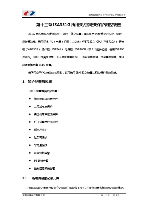
第十三章ISA381G所用变/接地变保护测控装置381G为所用变/接地变保护、测控一体化装置,实现所用变/接地变的保护、测控、操作等功能。
采用标准4U(半层)机箱,由交流(WB7181)、CPU(WB720A)、开出板(WB730B)、操作板(WB741)、电源板(WB760B)等5个插件组成,使用WB700总线板。
381G按面向对象、无人值班变电所设计,既可分散安装,也可集中组屏。
硬件原理同第六章351G装置。
当所用变不作为接地变使用时,也可选用ISA351G装置实现其保护测控功能。
1保护配置与说明381G装置提供的保护有:●相电流越限记录元件●二段过电流保护●高压侧零序过流保护●低压侧零序过流保护●低电压保护●过负荷保护●非电量保护●母线接地告警●PT断线告警●控制回路断线告警1.1相电流越限记录元件相电流越限记录元件设独立的越限门坎定值d797,并按相记录各相电流的越限情况。
1.2 二段过电流保护二段保护独立投退,电流及时间定值可独立整定,电流返回系数为0.95。
二段过电流保护原理除定值代码及事件代码不同外,逻辑关系完全相同,见图1。
d 053=投入 Ia>d055 Ib>d055 Ic>d055≥1&F025(数字信号) F025对应出口跳闸 中央信号一d056图1. Ⅰ段过电流保护逻辑框图1.3 低压侧零序过流保护低压侧零序保护配置二段可独立投退的定时限零序过流保护和反时限零序过流保护。
Ⅰ、Ⅱ段零序过流保护除定值代码及事件代码不同外,逻辑关系完全相同,见图2。
反时限零序过流保护提供一般反时限、非常反时限和极度反时限3种动作特性供选择。
3种动作特性如果同时投入,优先级排列从高到低为:极度反时限 > 非常反时限 > 一般反时限。
一般反时限特性方程为:1)(14.002.0-⨯=opo p I I T t ;非常反时限特性方程为:1)(5.13-⨯=op o p I I Tt ;极度反时限特性方程为:1)(802-⨯=opo p I I T t 。
HSMP-381B中文资料
Surface Mount RF PIN Low Distortion Attenuator DiodesTechnical DataFeatures•Diodes Optimized for:–Low Distortion Attenuating –Microwave FrequencyOperation•Surface Mount Packages–Single and Dual Versions–Tape and Reel OptionsAvailable•Low Failure in Time (FIT) Rate[1]•Lead-free Option Available Note:1.For more information see theSurface Mount PIN Reliability Data Sheet.HSMP-381x Series andHSMP-481x SeriesPackage Lead CodeIdentification, SOT-23(Top View)Description/Applications The HSMP-381x series is specifically designed for low distortion attenuator applica-tions. The HSMP-481x products feature ultra low parasitic inductance in the SOT-23 and SOT-323 packages. They are specifically designed for use at frequencies which are much higher than the upper limit for conventional diodes.A SPICE model is not available for PIN diodes as SPICE does not provide for a key PIN diode characteristic, carrier lifetime.SERIESSINGLEPackage Lead CodeIdentification, SOT-323(Top View)Absolute Maximum Ratings[1] T C = +25°CSymbol Parameter Unit SOT-23SOT-323I f Forward Current (1 µs Pulse)Amp11P IV Peak Inverse Voltage V Same as V BR Same as V BRT j Junction Temperature°C150150T stg Storage Temperature°C-65 to 150-65 to 150θjc Thermal Resistance[2]°C/W500150Notes:1.Operation in excess of any one of these conditions may result in permanent damage tothe device.2.T C = +25°C, where T C is defined to be the temperature at the package pins wherecontact is made to the circuit board.Electrical Specifications T C = +25°C (Each Diode)Conventional DiodesMinimum Maximum Maximum Minimum Maximum Part Package Breakdown Total Total High Low Number Marking Lead Voltage Resistance Capacitance Resistance Resistance HSMP-Code Code Configuration V BR (V)R T (Ω)C T (pF)R H (Ω)R L (Ω)3810E0[1]0Single100 3.00.35150010 3812E2[1]2Series3813E3[1]3Common Anode3814E4[1]4Common Cathode381B E0[2]B Single381C E2[2]C Series381E E3[2]E Common Anode381F E4[2]F Common CathodeTest Conditions V R = V BR I F = 100 mA V R = 50 V I R = 0.01 mA I F = 20 mAMeasure f = 100 MHz f = 1 MHz f = 100 MHz f= 100 MHzI R≤ 10 µAHigh Frequency (Low Inductance, 500 MHz – 3 GHz) PIN DiodesMinimum Maximum Typical Maximum Typical Part Package Breakdown Series Total Total Total Number Marking Lead Voltage Resistance Capacitance Capacitance Inductance HSMP-Code Code Configuration V BR (V)R S (Ω)C T (pF)C T (pF)L T (nH)4810EB B[1]Dual Cathode100 3.00.350.4 1.0 481B EB B[2]Dual CathodeTest Conditions V R = V BR I F = 100 mA V R = 50 V V R = 50 V f = 500 MHz–Measure f = 1 MHz f = 1 MHz 3 GHzI R≤ 10 µA V R = 0 VNotes:1.Package marking code is white.2.Package laser marked.Typical Parameters at T C = 25°CPart Number Series ResistanceCarrier LifetimeReverse Recovery TimeTotal CapacitanceHSMP-R S (Ω)τ (ns)T rr (ns)C T (pF)381x 7515003000.27 @ 50 V Test ConditionsI F = 1 mA I F = 50 mA V R = 10 V f = 1 MHzf = 100 MHzI R = 250 mAI F = 20 mA 90% RecoveryTypical Parameters at T C = 25°C (unless otherwise noted), Single DiodeR F R E S I S T A N C E (O H M S )0.010.1110100I F – FORWARD BIAS CURRENT (mA)Figure 2. RF Resistance vs. Forward Bias Current.2641012816141820T O T A L C A P A C I T A N C E (p F )REVERSE VOLTAGE (V)Figure 1. RF Capacitance vs. Reverse Bias.100010010DIODE RF RESISTANCE (OHMS)Figure 3. 2nd Harmonic Input Intercept Point vs. Diode RF Resistance.I N P U T I N T E R C E P T P O I N T (d B m )1001010.10.01I F – F O R W A R D C U R R E N T (m A )V F – FORWARD VOLTAGE (mA)Figure 4. Forward Current vs. Forward Voltage.INPUTFigure 5. Four Diode π Attenuator. See Application Note 1048 for Details.VOLTAGETypical Applications for Multiple Diode ProductsTypical Applications for HSMP-481x Low Inductance SeriesMicrostrip Series Connection for HSMP-481x SeriesIn order to take full advantage of the low inductance of the HSMP-481x series when using them in series applications,both lead 1 and lead 2 should be connected together, as shown inFigure 7.Figure 7. Circuit Layout.Figure 9. Equivalent Circuit.Figure 6. Internal Connections.HSMP-481xMicrostrip Shunt Connections forHSMP-481x SeriesIn Figure 8, the centerconductor of the microstrip line is interrupted and leads 1 and 2 of theHSMP-481x series diode are placed across the resulting gap. This forces the 1.5 nH lead inductance of leads 1 and 2 to appear as part of a low pass filter, reducing the shunt parasitic inductance and increasing the maximum available attenuation. The 0.3 nHof shunt inductanceexternal to the diode is created by the via holes, and is a good estimate for 0.032" thick material.GROUND BY TWOVIA HOLESFigure 8. Circuit Layout.Typical Applications for HSMP-481x Low Inductance Series (continued)Figure 10. Circuit Layout.Co-Planar Waveguide Shunt Connection for HSMP-481x SeriesCo-Planar waveguide, with ground on the top side of the printed circuit board, is shown in Figure 10. Since it eliminates the need for via holes to ground, it offers lower shunt parasitic inductance and higher maximum attenuation when compared to a microstrip circuit.Figure 11. Equivalent Circuit.0.18 pF** Measured at -20 VR j = 80ΩI 0.9R T C T = C P + C jI = Forward Bias Current in mA*See AN1124 for package models.Equivalent Circuit Model HSMS-381x Chip*Assembly InformationSOT-323 PCB FootprintA recommended PCB pad layout for the miniature SOT-323 (SC-70)package is shown in Figure 12(dimensions are in inches). This layout provides ample allowance for package placement by auto-mated assembly equipment without adding parasitics that could impair the performance.Figure 12. PCB Pad Layout (dimensions in inches).SOT-23 PCB FootprintFigure 13. PCB Pad Layout.TIME (seconds)T E M P E R A T U R E (°C )05010015020025060120180240300Figure 14. Surface Mount Assembly Profile.SMT AssemblyReliable assembly of surface mount components is a complex process that involves manymaterial, process, and equipment factors, including: method of heating (e.g., IR or vapor phase reflow, wave soldering, etc.)circuit board material, conductor thickness and pattern, type of solder alloy, and the thermalconductivity and thermal mass of components. Components with a low mass, such as the SOT-323/-23package, will reach solder reflow temperatures faster than those with a greater mass.Agilent ’s diodes have beenqualified to the time-temperature profile shown in Figure 14. This profile is representative of an IR reflow type of surface mount assembly process.After ramping up from room temperature, the circuit board with components attached to it (held in place with solder paste)passes through one or morepreheat zones. The preheat zones increase the temperature of the board and components to prevent thermal shock and begin evaporat-ing solvents from the solder paste.The reflow zone briefly elevates the temperature sufficiently to produce a reflow of the solder.The rates of change of tempera-ture for the ramp-up and cool-down zones are chosen to be low enough to not cause deformation of the board or damage to compo-nents due to thermal shock. The maximum temperature in the reflow zone (T MAX ) should not exceed 235°C.These parameters are typical for a surface mount assembly process for Agilent diodes. As a general guideline, the circuit board and components should be exposed only to the minimum tempera-tures and times necessary to achieve a uniform reflow of solder.Package DimensionsOutline SOT-323 (SC-70)Package CharacteristicsLead Material...................................Copper (SOT-323); Alloy 42 (SOT-23)Lead Finish............................................................................Tin-Lead 85-15%Maximum Soldering Temperature..............................260°C for 5 seconds Minimum Lead Strength..........................................................2 pounds pull Typical Package Inductance ..................................................................2 nH Typical Package Capacitance ..............................0.08 pF (opposite leads)Outline 23 (SOT-23)Ordering InformationSpecify part number followed by option. For example:HSMP -381x -XXXBulk or Tape and Reel Option Part Number; x = Lead Code Surface Mount PINOption Descriptions-BLK = Bulk, 100 pcs. per antistatic bag-TR1 = Tape and Reel, 3000 devices per 7" reel -TR2 = Tape and Reel, 10,000 devices per 13" reelTape and Reeling conforms to Electronic Industries RS-481, “Taping of Surface Mounted Components for Automated Placement.”For lead-free option, the part number will have the character "G" at the end, eg. -TR2G for a 10K pc lead-free reel.0.30 (0.012)0.10 (0.004)0.425 (0.017)DIMENSIONS ARE IN MILLIMETERS (INCHES)SIDE VIEWEND VIEWDIMENSIONS ARE IN MILLIMETERS (INCHES)Tape Dimensions and Product OrientationFor Outline SOT-23Note: "AB" represents package marking code. "C" represents date code.END VIEWTOP VIEWDevice OrientationFor Outlines SOT-23/323USER FEEDDESCRIPTIONSYMBOL SIZE (mm)SIZE (INCHES)LENGTH WIDTH DEPTH PITCHBOTTOM HOLE DIAMETER A 0B 0K 0P D 1 3.15 ± 0.102.77 ± 0.101.22 ± 0.104.00 ± 0.101.00 + 0.050.124 ± 0.0040.109 ± 0.0040.048 ± 0.0040.157 ± 0.0040.039 ± 0.002CAVITYDIAMETER PITCH POSITION D P 0E 1.50 + 0.104.00 ± 0.101.75 ± 0.100.059 + 0.0040.157 ± 0.0040.069 ± 0.004PERFORATIONWIDTH THICKNESSW t18.00 + 0.30 – 0.100.229 ± 0.0130.315 + 0.012 – 0.0040.009 ± 0.0005CARRIER TAPE CAVITY TO PERFORATION (WIDTH DIRECTION)CAVITY TO PERFORATION (LENGTH DIRECTION)F P 23.50 ± 0.052.00 ± 0.050.138 ± 0.0020.079 ± 0.002DISTANCE BETWEEN CENTERLINE/semiconductorsFor product information and a complete list of distributors, please go to our web site.For technical assistance call:Americas/Canada: +1 (800) 235-0312 or (916) 788-6763Europe: +49 (0) 6441 92460China: 10800 650 0017Hong Kong: (65) 6756 2394India, Australia, New Zealand: (65) 6755 1939Japan: (+81 3) 3335-8152(Domestic/International), or 0120-61-1280(Domestic Only)Korea: (65) 6755 1989Singapore, Malaysia, Vietnam, Thailand, Philippines,Indonesia: (65) 6755 2044Taiwan: (65) 6755 1843Data subject to change.Copyright © 2004 Agilent Technologies, Inc.Obsoletes 5968-5427E March 24, 20045989-0482EN(CARRIER TAPE THICKNESS)(COVER TAPE THICKNESS)DESCRIPTIONSYMBOL SIZE (mm)SIZE (INCHES)LENGTH WIDTH DEPTH PITCHBOTTOM HOLE DIAMETER A 0B 0K 0P D 1 2.40 ± 0.102.40 ± 0.101.20 ± 0.104.00 ± 0.101.00 + 0.250.094 ± 0.0040.094 ± 0.0040.047 ± 0.0040.157 ± 0.0040.039 + 0.010CAVITYDIAMETER PITCH POSITION D P 0E 1.55 ± 0.054.00 ± 0.101.75 ± 0.100.061 ± 0.0020.157 ± 0.0040.069 ± 0.004PERFORATIONWIDTH THICKNESS W t 18.00 ± 0.300.254 ± 0.020.315 ± 0.0120.0100 ± 0.0008CARRIER TAPE CAVITY TO PERFORATION (WIDTH DIRECTION)CAVITY TO PERFORATION (LENGTH DIRECTION)F P 2 3.50 ± 0.052.00 ± 0.050.138 ± 0.0020.079 ± 0.002DISTANCEFOR SOT-323 (SC70-3 LEAD)An8°C MAX FOR SOT-363 (SC70-6 LEAD)10°C MAXANGLEWIDTHTAPE THICKNESS C T t 5.4 ± 0.100.062 ± 0.0010.205 ± 0.0040.0025 ± 0.00004COVER TAPE Tape Dimensions and Product OrientationFor Outline SOT-323。
HSMP-3862中文资料
Surface Mount PIN Diodes Technical DataFeatures•Diodes Optimized for:Low Current SwitchingLow Distortion AttenuatingUltra-Low DistortionSwitchingMicrowave FrequencyOperation•Surface Mount SOT-23 and SOT-143 PackagesSingle and Dual VersionsTape and Reel OptionsAvailable•Low Failure in Time (FIT) Rate[1]Note:1.For more information see theSurface Mount PIN Reliability Data Sheet.HSMP-38XX andHSMP-48XX SeriesPackage Lead CodeIdentificationrequired. The HSMP-48XX seriesare special products featuringultra low parasitic inductance inthe SOT-23 package, specificallydesigned for use at frequencieswhich are much higher than theupper limit for conventionalSOT-23 PIN diodes. TheHSMP-4810 diode is a low distor-tion attenuating PIN designed foroperation to 3 GHz. TheHSMP-4820 diode is ideal forlimiting and low inductanceswitching applications up to1.5GHz. The HSMP-4890 isoptimized for low current switch-ing applications up to 3 GHz.The HSMP-386X series of generalpurpose PIN diodes are designedfor two classes of applications.The first is attenuators wherecurrent consumption is the mostimportant design consideration.The second application for thisseries of diodes is in switcheswhere low cost is the drivingissue for the designer.The HSMP-386X series TotalCapacitance (C T) and TotalResistance (R T) are typicalspecifications. For applicationsthat require guaranteed perfor-mance, the general purposeHSMP-383X series is recom-Description/Applications The HSMP-380X and HSMP-381X series are specifically designed for low distortion attenuator applica-tions. The HSMP-382X series is optimized for switching applica-tions where ultra-low resistance is required. The HSMP-3880 switch-ing diode is an ultra low distortion device optimized for higher power applications from 50 MHz to1.5GHz. The HSMP-389X series is optimized for switching applica-tions where low resistance at low attenuators, the HSMP-380X or -381X series are recommended. For high performance switching applications, the HSMP-389X series is recommended.A SPICE model is not available for PIN diodes as SPICE does not provide for a key PIN diode characteristic, carrier lifetime.Absolute Maximum Ratings [1] T A = 25°CSymbol ParameterUnits Absolute Maximum I f Forward Current (1 ms Pulse)Amp 1P t Total Device Dissipation mW [2]250P iv Peak Inverse Voltage —Same as V BRT j Junction Temperature °C 150T STGStorage Temperature°C-65 to 150Notes:1.Operation in excess of any one of these conditions may result in permanent damage to this device.2.CW Power Dissipation at T LEAD = 25°C. Derate to zero at maximum rated temperature.PIN Switching DiodesElectrical Specifications T A = 25°CNearest Maximum Equivalent Minimum Maximum Maximum Shunt Mode Part Package Axial Lead Breakdown Series Total Harmonic Number Marking LeadPart No.Voltage Resistance Capacitance Distortion HSMP-Code [1]Code Configuration 5082-V BR (V)R S (Ω)C T (pF)Hmd (dBc)3820F00Single 3188500.6*0.8*—3822F22Series3823F33Common Anode 3824F44Common Cathode 3880S00Single—100 6.50.40–553890G00Single —1002.50.30**—3892G22Series3893G33Common Anode 3894G44Common Cathode 3895G55Unconnected PairTest ConditionsV R = V BR I F = 5 mA V R = 50 V 2 f o, Z o = 50 W Measure f = 100 MHz f = 1 MHz f o = 400 MHz I R ≤ 10 µA I F = 10 mA*V R = 20 V*P in = +30 dBm V R = 5 V**0 V biasPIN Attenuator DiodesElectrical Specifications T A = 25°C (Each Diode)NearestEquivalent Minimum Maximum Maximum Minimum Maximum Part Package Axial Lead Breakdown Series Total High Low Number Marking LeadPart No.Voltage Resistance Capacitance Resistance Resistance HSMP-Code [1]Code Configuration 5082-V BR (V)R S (Ω)C T (pF)R H (Ω)R L (Ω)3800D00Single 30801002.00.37100083802D22Series3804D44Common Cathode 3810E00Single 3081100 3.00.351500103812E22Series3813E33Common Anode 3814E44Common CathodeTest ConditionsV R = V BR I F = 100 mA V R = 50 V I F = 0.01 mA I F = 20 mA Measure f = 100 MHz f = 1 MHz f = 100 MHz f= 100 MHzI R ≤ 10 µAPIN General Purpose Diodes, Electrical Specifications T A = 25°CNearestEquivalent Minimum Maximum Maximum Part Package Axial Lead Breakdown Series Total Number Marking Lead Part No.Voltage Resistance Capacitance HSMP-Code[1]Code Configuration5082-V BR (V)R S (Ω)C T (pF) 3830K00Single3077200 1.50.3 3832K22Series3833K33Common Anode3834K44Common CathodeTest Conditions V R = V BR I F = 100 mA V R = 50 VMeasure f = 100 MHz f = 1 MHzI R≤ 10 mAHigh Frequency (Low Inductance, 500 MHz – 3 GHz) PIN Diodes, Electrical Specifications T A = 25°CMinimum Maximum Typical Maximum TypicalBreak-Series Total Total Total Part Package down Resis-Capaci-Capaci-Induc-Number Marking Lead Config-Voltage tance tance tance tance Appli-HSMP-Code Code uration V BR (V)R S (Ω)C T (pF)C T (pF)L T (nH)cation 4810EB B Dual100 3.00.350.4 1.0Attenu-Cathode ator 4820FA A Dual Anode500.6*0.75* 1.0 1.0*Limiter 4890GA A Dual Anode100 2.5**0.330.375 1.0SwitchV R = V BR I F = 100 mA V R = 50 V V R = 50 V f = 500 MHz –Measure I F = 10 mA* f = 1 MHz f = 1 MHz 3 GHzI R≤ 10 µA I F = 5 mA**V R = 20 V*V R = 0 V V R = 20 V*PIN General Purpose Diodes, Typical Specifications T A = 25°CCode Minimum Typical Series Typical Total Part Number Marking Lead Breakdown Resistance Capacitance HSMP-Code[1]Code Configuration Voltage V BR (V)R S (Ω)C T (pF)3860L00Single50 3.0/1.5*0.203862L22Series3863L33Common Anode3864L44Common CathodeTest Conditions V R = V BR I F = 10 mA V R = 50 VMeasure f = 100 MHz f = 1 MHzI R≤ 10 µA*I F = 100 mATypical Parameters at T A = 25°CPart Number Series Resistance Carrier Lifetime Reverse Recovery Time Total Capacitance HSMP-R S (Ω)τ (ns)T rr (ns)C T (pF)380X5518005000.32 @ 50 V381X7515003000.27 @ 50 V382X 1.570*70.60 @ 20 V383X20500800.20 @ 50 V388X 3.825005500.30 @ 50 V389X 3.8200*–0.20 @ 5 V Test Conditions I F = 1 mA I F = 50 mA V R = 10 Vf = 100 MHz I R = 250 mA I F = 20 mAI F = 10 mA*I F = 10 mA*90% RecoveryI R = 6 mA*Typical Parameters at T A = 25°C (unless otherwise noted), Single DiodeFigure 2. RF Capacitance vs. Reverse Bias, HSMP-3830 Series.0.150.300.250.200.350.400.45T O T A L C A P A C I T A N C E (p F )REVERSE VOLTAGE (V)Figure 1. RF Capacitance vs. Reverse Bias, HSMP-3810 Series.Figure 3. Resistance at 25°C vs. Forward Bias Current.0.150.300.250.200.35T O T A L C A P A C I T A N C E (p F )REVERSE VOLTAGE (V)R E S I S T A N C E (O H M S )I F – FORWARD BIAS CURRENT (mA)0.010.11101000.010.1110100R F R E S I S T A N C E (O H M S )I F – FORWARD BIAS CURRENT (mA)R F R E S I S T A N C E (O H M S )0.010.1110100I F – FORWARD BIAS CURRENT (mA)Figure 5. RF Resistance vs. Forward Bias Current for HSMP-3810/HSMP-4810.V R – REVERSE VOLTAGE (V)C A P A C I T A N C E (p F )Figure 6. Capacitance vs. Reverse Voltage.Figure 4. RF Resistance vs. Forward Bias Current for HSMP-3800.100010010DIODE RF RESISTANCE (OHMS)Figure 7. 2nd Harmonic Input Intercept Point vs. Diode RFResistance for Attenuator Diodes.I N P U T I N T E R C E P T P O I N T (d B m )12011511010510095908511030I F – FORWARD BIAS CURRENT (mA)Figure 8. 2nd Harmonic Input Intercept Point vs. Forward Bias Current for Switch Diodes.I N P U T I N T E R C E P T P O I N T (d B m )FORWARD CURRENT (mA)Figure 9. Reverse Recovery Time vs. Forward Current for Various Reverse Voltages. HSMP-3820 Series.T r r – R E V E R S E R E C O V E R Y T I M E (n s )110100102030V R = 2V V R = 5VV R = 10VHSMP-382XTypical Parameters (continued)100010010102030T r r - R E V E R S E R E C O V E R Y T I M E (n S )FORWARD CURRENT (mA)Figure 10. Reverse Recovery Time vs. Forward Current for Various Reverse Voltage. HSMP-3830 Series.HSMP-3830V R = 5VV R = 10V V R = 20VR E V E R S E R E C O V E R Y T I M E (n S )FORWARD CURRENT (mA)Figure 11. Typical Reverse Recovery Time vs. Reverse Voltage. HSMP-3880 Series.1020152530T R R - R E V E R S E R E C O V E R Y T I M E (n S )FORWARD CURRENT (mA)Figure 12. Typical Reverse Recovery Time vs. Reverse Voltage. HSMP-3890 Series.1001010.10.01I F – F O R W A R D C U R R E N T (m A )I F – F O R W A R D C U R R E N T (m A )V F – FORWARD VOLTAGE (mA)Figure 14. Forward Current vs. Forward Voltage. HSMP-3810 and HSMP-4810 Series.V F – FORWARD VOLTAGE (mA)Figure 15. Forward Current vs. Forward Voltage. HSMP-3820 and HSMP-4820 Series.1001010.10.01I F – F O R W A R D C U R R E N T (m A )V F – FORWARD VOLTAGE (mA)Figure 16. Forward Current vs.Forward Voltage. HSMP-3830 Series.00.20.40.60.81.01.2I F – F O R W A R D C U R R E N T (m A )V F – FORWARD CURRENT (mA)Figure 17. Forward Current vs.Forward Voltage. HSMP-3880 Series.0.20.40.60.81.01.2V F – FORWARD VOLTAGE (mA)Figure 18. Forward Current vs. Forward Voltage. HSMP-3890 and HSMP-4890 Series.Typical Parameters (continued)Figure 19. Typical RF Resistance vs. Forward Bias Current for HSMP-3860.Figure 20. Forward Current vs. Forward Voltage for HSMP-3860.Figure 21. Typical Capacitance vs. Reverse Bias for HSMP-3860.10001R E S I S T A N C E (O HM S )BIAS CURRENT (mA)10100I F – F O R W A R D C U R R E N T (m A )V F – FORWARD VOLTAGE (V)0200.515C T – C A P A C I T A N C E (p F )V R – REVERSE VOLTAGE (V)0.20.41050.10.30.12 pF** Measured at -20 V C p 0.08 pFR j = 12ΩI 0.9C T = C P + C jI = Forward Bias Current in mAEquivalent Circuit ModelHSMS-3860Typical Applications for Multiple Diode ProductsRF COMMONRF 1RF 1Figure 24. Switch Using Both Positive and Negative Bias Current.Figure 25. Very High Isolation SPDT Switch, Dual Bias.Typical Applications for Multiple Diode Products (continued)INPUT RF IN/OUTFigure 26. Four Diode π Attenuator.Figure 27. High Isolation SPST Switch (Repeat Cells as Required).VOLTAGEBIASFigure 28. Power Limiter Using HSMP-3822Diode Pair.Typical Applications for HSMP-48XX Low Inductance SeriesFigure 29. Internal Connections.HSMP-4820 & HSMP-4890HSMP-48100.5 nH*0.8pF TYPICAL FOR HSMP-3820Figure 30. Equivalent Circuit.*0.8 pF TYPICAL FOR HSMP-3820Figure 32. Equivalent Circuit.Figure 31. Circuit Layout.Microstrip SeriesConnection for HSMP-48XX SeriesIn order to take full advantage of the low inductance of the HSMP-48XX series when using them in series application,both lead 1 and lead 2 should beconnected together, as shown above.Microstrip Shunt Connections for HSMP-48XX SeriesIn the diagram above, the center conductor of themicrostrip line is interrupted and leads 1 and 2 of theHSMP-38XX series diode are placed across the resulting gap. This forces the 0.5 nH lead inductance of leads 1 and 2 to appear as part of a low pass filter, reducing the shunt parasitic inductance andincreasing the maximumavailable attenuation. The 0.3 nH of shunt inductance external to the diode is created by the via holes, and is a good estimate for 0.032" thick material.Co-Planar Waveguide Shunt Connection for HSMP-48XX SeriesCo-Planar waveguide, with ground on the top side of the printed circuit board, is shownin the diagram above. Since it eliminates the need for via holes to ground, it offers lower shunt parasitic inductance and higher maximum attenuation whencompared to a microstrip circuit.GROUND BY TWOVIA HOLES*0.8 pF TYPICAL FOR HSMP-4820Figure 34. Equivalent Circuit.Figure 33. Circuit Layout.*0.8 pF TYPICAL FOR HSMP-4820Figure 36. Equivalent Circuit.Figure 35. Circuit Layout.11Package DimensionsOutline 23 (SOT-23)PC Board FootprintsSOT-23Package CharacteristicsLead Material......................................................................................Alloy 42Lead Finish............................................................................Tin-Lead 85-15%Maximum Soldering Temperature..............................260°C for 5 seconds Minimum Lead Strength..........................................................2 pounds pull Typical Package Inductance ..................................................................2 nH Typical Package Capacitance ..............................0.08 pF (opposite leads)SOT-143Outline 143 (SOT-143)SIDE VIEWEND VIEWDIMENSIONS ARE IN MILLIMETERS (INCHES)DIMENSIONS ARE IN MILLIMETERS (INCHES)PACKAGE MARKING/go/rfFor technical assistance or the location of your nearest Hewlett-Packard salesoffice, distributor or representative call:Americas/Canada: 1-800-235-0312 or 408-654-8675Far East/Australasia: Call your local HP sales office.Japan: (81 3) 3335-8152Europe: Call your local HP sales office.Data subject to change.Copyright © 1999 Hewlett-Packard Co.Obsoletes 5968-3435E5968-5439E (6/99)Profile Option Descriptions-BLK = Bulk-TR1 = 3K pc. Tape and Reel, Device Orientation; See Figures 37 and 38-TR2 = 10K pc. Tape and Reel, Device Orientation; See Figures 37 and 38Tape and Reeling conforms to Electronic Industries RS-481, “Taping of Surface Mounted Components for Automated Placement.”Ordering InformationSpecify part number followed by option under. For example:H SMP -38XX -XXXBulk or Tape and Reel OptionPart NumberSurface Mount PIN Diode Hewlett-PackardUSER FEEDEND VIEWTOP VIEW Figure 37. Options -TR1, -TR2 for SOT-23 Packages.Figure 38. Options -TR1, -TR2 for SOT-143 Packages.END VIEWTOP VIEW。
381LR331M200H022中文资料
SpecificationsOperating Temperature: –40 °C to + 105 °C ≤ 315 Vdc –25 °C to + 105 °C ≥ 350 Vdc Rated Voltage: 200 to 450 VdcCapacitance: 56 µF to 2,200 µF ± 20%Leakage Current: ≤3 √CV µA, 4 mA max, 5 minutes Ripple Current Multipliers: Ambient TemperatureFrequency EIA Ripple Life: 10,000 h at 85 °C, full load per EIA IS-749 ∆ Capacitance ±20%ESR 200% of limit DCL 100% of limitLoad LifeTest: 3000 h at full load at 105 °C∆Capacitance 20% ESR 200% of limitDCL 100% of limit Shelf Life:1000 h at 105 °C∆Capacitance 20% ESR 200% of limitDCL 100% of limitVibration:10 to 55 Hz, 0.06" and 10 g max, 2 h each planeCompared to standard 105 °C snap-ins like the Type 381L/LX Type 381LR can handle an extra 25% ripple current or more. This remarkable capability stems from advances in electrolyte that give extremely low ESR values.In high ripple current applications like motor drives you can save by using fewer capacitors.HighlightsThe right choice for motor drive bus capacitors The right choice for UPS bus capacitors Compare to Type 381LUp to 2 times the ripple current••••25% More Ripple Current Capability45 ºC 60 ºC 70 ºC 85 ºC 105 ºC 2.35 2.202.001.701.0050Hz 60 Hz 120 Hz 500 Hz 1 kHz 10 kHz & up 0.750.801.001.201.251.40Insulated Case DimensionsOutline DrawingPart Numbering System380LRType 271Capacitance271 = 270 µF 222 = 2200 µFMToleranceM = ±20%200Rated Voltage160 = 160 V 450 = 450 VH012Case Code 2=PVCTypical Performance CurvesDIAMETER D LENGTHTypical DIAMETERD LENGTHTypical Case LWeight Case LWeight Code mm inches mm inches (grams)Code mm inches mm inches (grams)H01220.87250.9816K0130 1.18250.9830H02220.8730 1.1819K0230 1.1830 1.1835H03220.8735 1.3822K0330 1.1835 1.3840H04220.8740 1.5724K0430 1.1840 1.5744H45220.8745 1.7728K4530 1.1845 1.7749H05220.8750 1.9731K0530 1.1850 1.9753J01250.98250.9820A0135 1.38250.9842J02250.9830 1.1824A0235 1.3830 1.1848J03250.9835 1.3827A0335 1.3835 1.3854J04250.9840 1.5731A0435 1.3840 1.5760J45250.9845 1.7735A4535 1.3845 1.7767J05250.98501.9738A05351.38501.9774ESR Max @ 25º CRipple Amps@ 105 ºCNominalSize D x L (mm)ESR Max @ 25º CRipple Amps@ 105 ºCNominalSize D x L (mm)Cap.(µF)Catalog Part Number120 Hz (Ω)20 kHz (Ω)120 Hz (A)20 kHz (A)Cap.(µF)Catalog Part Number120 Hz (Ω)20 kHz (Ω)120 Hz (A)20 kHz (A)200 Vdc (250 Vdc Surge)400 Vdc (450 Vdc Surge)270381LR271M200H012 0.5530.249 1.42 2.0322 X 25 220381LR221M400A012 0.6030.271 1.42 2.0335 X 25 330381LR331M200H022 0.4520.203 1.56 2.2322 X 30 270381LR271M400J452 0.4910.221 1.56 2.2325 X 45 390381LR391M200H022 0.3830.172 1.71 2.4422 X 30 270381LR271M400K032 0.4910.221 1.56 2.2330 X 35 390381LR391M200J012 0.3830.172 1.71 2.4425 X 25 270381LR271M400A022 0.4910.221 1.56 2.2335 X 30 470381LR471M200H032 0.3170.143 1.85 2.6422 X 35 330381LR331M400K042 0.4020.181 1.71 2.4430 X 40 470381LR471M200J022 0.3170.143 1.85 2.6425 X 30 330381LR331M400A022 0.4020.181 1.71 2.4435 X 30 560381LR561M200H042 0.2660.120 2.14 3.0522 X 40 390381LR391M400K452 0.340.153 1.85 2.6430 X 45 560381LR561M200J022 0.2660.120 2.14 3.0525 X 30 390381LR391M400A032 0.340.153 1.85 2.6435 X 35 560381LR561M200K012 0.2660.120 2.14 3.0530 X 25 470381LR471M400A042 0.2820.127 2.01 2.8735 X 40 680381LR681M200H452 0.2190.099 2.42 3.4522 X 45 560381LR561M400A452 0.2370.107 2.35 3.3635 X 45 680381LR681M200J032 0.2190.099 2.42 3.4525 X 35 420 Vdc (470 Vdc Surge)680381LR681M200K022 0.2190.099 2.42 3.4530 X 30 68381LR680M420H012 1.950.8780.76 1.0822 X 25 820381LR821M200H052 0.1820.082 2.63 3.7622 X 50 82381LR820M420H022 1.6170.7280.8 1.1422 X 30 820381LR821M200J042 0.1820.082 2.63 3.7625 X 40 82381LR820M420J012 1.6170.7280.8 1.1425 X 25 820381LR821M200K022 0.1820.082 2.63 3.7630 X 30 10038L1R101M420H022 1.3260.5970.91 1.322 X 30 820381LR821M200A012 0.1820.082 2.63 3.7635 X 25 100381LR101M420J012 1.3260.5970.91 1.325 X 25 1000381LR102M200J452 0.1490.067 2.84 4.0625 X 45 120381LR121M420H032 1.1050.497 1.02 1.4622 X 35 1000381LR102M200K032 0.1490.067 2.84 4.0630 X 35 120381LR121M420J022 1.1050.497 1.02 1.4625 X 30 1000381LR102M200A022 0.1490.067 2.84 4.0635 X 30 150381LR151M420H042 0.8840.398 1.07 1.5322 X 40 1200381LR122M200K042 0.1240.062 3.13 4.4730 X 40 150381LR151M420J032 0.8840.398 1.07 1.5325 X 35 1200381LR122M200A032 0.1240.062 3.13 4.4735 X 35 150381LR151M420K012 0.8840.398 1.07 1.5330 X 25 1500381LR152M200K052 0.0990.050 3.56 5.0630 X 50 180381LR181M420H452 0.7370.332 1.12 1.622 X 45 1500381LR152M200A042 0.0990.050 3.56 5.0635 X 40 180381LR181M420J042 0.7370.332 1.12 1.625 X 401800381LR182M200A452 0.0830.041 3.84 5.4835 X 45180381LR181M420K022 0.7370.332 1.12 1.630 X 30 2200381LR222M200A052 0.0660.040 4.12 5.8935 X 50 180381LR181M420A012 0.7370.332 1.12 1.635 X 25 250 Vdc (300 Vdc Surge)220381LR221M420J452 0.6030.271 1.42 2.0325 X 45 220381LR221M250H022 0.6780.305 1.28 1.8322 X 30 220381LR221M420K032 0.6030.271 1.42 2.0330 X 35 270381LR271M250H022 0.5530.249 1.42 2.0322 X 30 220381LR221M420A022 0.6030.271 1.42 2.0335 X 30 270381LR271M250J012 0.5530.249 1.42 2.0325 X 25 270381LR271M420J052 0.4910.221 1.68 2.425 X 50 330381LR331M250H032 0.4520.203 1.64 2.3422 X 35 270381LR271M420K042 0.4910.221 1.68 2.430 X 40 330381LR331M250J022 0.4520.203 1.64 2.3425 X 30 270381LR271M420A022 0.4910.221 1.68 2.435 X 30 390381LR391M250H042 0.3830.172 1.72 2.4522 X 40 330381LR331M420K452 0.4020.181 1.78 2.5430 X 45 390381LR391M250J022 0.3830.172 1.72 2.4525 X 30 330381LR331M420A032 0.4020.181 1.78 2.5435 X 35 390381LR391M250K012 0.3830.172 1.72 2.4530 X 25 390381LR391M420K052 0.340.153 1.91 2.7330 X 50 470381LR471M250H452 0.3170.143 1.85 2.6422 X 45 390381LR391M420A042 0.340.153 1.91 2.7335 X 40 470381LR471M250J032 0.3170.143 1.85 2.6425 X 35 470381LR471M420A452 0.2820.127 2.23 3.1835 X 45 470381LR471M250K022 0.3170.143 1.85 2.6430 X 30 450 Vdc (500 Vdc Surge)560381LR561M250J042 0.2660.120 2.14 3.0525 X 40 56381LR560M450H012 2.368 1.0660.670.9522 X 25 560381LR561M250K022 0.2660.120 2.14 3.0530 X 30 68381LR680M450H022 1.950.8780.76 1.0822 X 30 560381LR561M250A012 0.2660.120 2.14 3.0535 X 25 68381LR680M450J012 1.950.8780.76 1.0825 X 25 680381LR681M250J452 0.2190.099 2.42 3.4525 X 45 82381LR820M450H022 1.6170.7280.8 1.1422 X 30 680381LR681M250K032 0.2190.099 2.42 3.4530 X 35 82381LR820M450J012 1.6170.7280.8 1.1425 X 25 680381LR681M250A022 0.2190.099 2.42 3.4535 X 30 100381LR101M450H032 1.3260.5970.91 1.322 X 35 820381LR821M250K042 0.1820.082 2.63 3.7630 X 40 100381LR101M450J022 1.3260.5970.91 1.325 X 30 820381LR821M250A032 0.1820.082 2.63 3.7635 X 35 120381LR121M450H042 1.1050.497 1.02 1.4622 X 40 1000381LR102M250K052 0.1490.067 2.84 4.0630 X 50 120381LR121M450J032 1.1050.497 1.02 1.4625 X 35 1000381LR102M250A042 0.1490.067 2.84 4.0635 X 40 120381LR121M450K012 1.1050.497 1.02 1.4630 X 25 1200381LR122M250A452 0.1240.062 3.13 4.4735 X 45 150381LR151M450H452 0.8840.396 1.07 1.5322 X 45 1500381LR152M250A052 0.0990.050 3.56 5.0635 X 50 150381LR151M450J042 0.8840.396 1.07 1.5325 X 40 400 Vdc (450 Vdc Surge)150381LR151M450K022 0.8840.396 1.07 1.5330 X 30 82381LR820M400H012 1.6170.7280.8 1.1422 X 25 150381LR151M450A012 0.8840.396 1.07 1.5335 X 25 100381LR101M400H022 1.3260.5970.91 1.322 X 30 180381LR181M450H052 0.7370.332 1.12 1.622 X 50 100381LR101M400J012 1.3260.5970.91 1.325 X 25 180381LR181M450J042 0.7370.332 1.12 1.625 X 40 120381LR121M400H032 1.1050.497 1.02 1.4622 X 35 180381LR181M450K022 0.7370.332 1.12 1.630 X 30 120381LR121M400J022 1.1050.497 1.02 1.4625 X 30 180381LR181M450A012 0.7370.332 1.12 1.635 X 25 150381LR151M400H042 1.1050.387 1.07 1.5322 X 40 220381LR221M450J452 0.6030.271 1.42 2.0325 X 45 150381LR151M400J022 1.1050.387 1.07 1.5325 X 30 220381LR221M450K032 0.6030.271 1.42 2.0330 X 35 150381LR151M400K012 1.1050.387 1.07 1.5330 X 25 220381LR221M450A022 0.6030.271 1.42 2.0335 X 30 180381LR181M400H452 0.7370.322 1.12 1.622 X 45 270381LR271M450K042 0.4910.221 1.72 2.4530 X 40 180381LR181M400J032 0.7370.322 1.12 1.625 X 35 270381LR271M450A032 0.4910.221 1.72 2.4535 X 35 180381LR181M400K022 0.7370.322 1.12 1.630 X 30 330381LR331M450K052 0.4020.181 1.85 2.6430 X 50 220381LR221M400H052 0.6030.271 1.42 2.0322 X 50 330381LR331M450A042 0.4020.181 1.85 2.6435 X 40 220381LR221M400J042 0.6030.271 1.42 2.0325 X 40 390381LR391M450A042 0.340.153 1.97 2.8235 X 40 220381LR221M400K0220.6030.2711.422.0330 X 30470381LR471M450A0520.2820.1272.473.5335 X 50Ratings RoHS Compliant。
BD3801FS中文资料
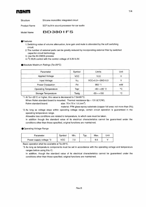
The products listed in this document are designed to be used with ordinary electronic equipment or devices (such as audio visual equipment, office-automation equipment, communications devices, electrical appliances and electronic toys). Should you intend to use these products with equipment or devices which require an extremely high level of reliability and the malfunction of with would directly endanger human life (such as medical instruments, transportation equipment, aerospace machinery, nuclear-reactor controllers, fuel controllers and other safety devices), please be sure to consult with our sales representative in advance. About Export Control Order in Japan Products described herein are the objects of controlled goods in Annex 1 (Item 16) of Export Trade Control Order in Japan. In case of export from Japan, please confirm if it applies to "objective" criteria or an "informed" (by MITI clause) on the basis of "catch all controls for Non-Proliferation of Weapons of Mass Destruction.
3810、3410系列电动执行器381LSA-08381LSA-20

3810、3410系列电子式电动执行器一、结构特点和应用范围3810系列电子式电动执行器,是以220V 交流单相电源作为驱动电源,接受来自计算机调节器或操作 器的4-20mADC ,或者1-5VDC 输入信号来运转的全电子式执行机构,机内有伺服系统,无需另配伺服放大器,关键部件“控制器”采用先进的混合集成电路,并用树脂浇铸固化,经老化处理,可靠性高,防潮,防震。
用电位器调整零点、行程、灵敏度,方便易行;用功能开关任意选择正、反动作、选择断信号的三种状态。
同时,执行器具有过载保护、温度保护及压缩弹簧保证阀门的关严等三种保护功能。
是一种具有高可靠性的产品,可与各种直行程和角行程调节阀门组成电动调节阀。
3410系列电子式电动执行器是以220V 交流单相电源为驱动电源,输入信号采用220V 交流开关,电机采用交流可逆单相齿轮减速电机,开度检测采用精密导电塑料定位器,可与各种直行程和角行程调节阀门组成开关控制型电动执行器。
二、直行程3810L 、3410L 系列类别3810L 系列3410L 系列额定输出力N速度mm/s 最大行程mm 普通型381LS A-08 341LS A-08 800 4.2 30 381LSA-20341LSA-20 2000 2.1 381LSB-30 341LSB-30 3000 3.5 60 381LS B-50 341LS B-50 5000 1.7 381LSC-65 341LSC-65 6500 3.4 100381LSC-99 341LSC-99 10000 2.0 381LSC-160341LSC-160 16000 1.0 隔爆型381LX A-08 341LX A-08 800 4.2 30 381LXA-20 341LXA-20 2000 2.1 381LXA-30 341LXA-30 3000 3.5 60 381LXA-50341LXA-5050001.7三、角行程3810R 、3410R 系列防爆型类别3810R 系列 3410R 系列 额定输出力矩N.m 动作时间90o/S 最大转角普通型381RSA-02 341RSA-02 20 8.5 90º381RSA-05 341RSA-05 50 17 381RSB-10 341RSB-10 100 18 381RSB-20 341RSB-20 200 36 381RSC-30 341RSC-30 300 24 381RSC-50 341RSC-50 500 42 381RSC-60 341RSC-60 600 48 381RSD-100 341RSD-100 1000 30 381RSD-150 341RSD-150 1500 42 隔爆型 381RSXB-10 341RSXB-10 10018 381RSXB-20341RSXB-2020036四、主要技术参数参数名称3810系列3410系列控制机构输入信号4~20mADC或1~5VDC 220V AC开关信号开度信号4~20mADC(负荷电阻500Ω以下) 反馈4~20mADC或0~1.0KΩ死区0.8~1.0%可调到0.4%零点调整25%量程调整20~100%基本误差、回差 1.0%控制限位、开关开侧、闭侧开侧、闭侧开度检测精密导电塑料电位器精密导电塑料电位器动力电源AC220±10% 50Hz AC220±10% 50Hz 驱动电机AC可逆单相齿轮减速电机AC可逆单相齿轮减速电机耗电功率A型50 V A 50 V AB型150 VA 150 VAC型220 VA 220 VAD型350V A 350V A附属机构过载保护单元A、B型任选,C、D型必备力矩开关角行程可以安装(选择件)角行程可以安装(选择件)空间加热器选择件,但防爆型不装选择件,但防爆型不装手动机构便携式手动曲柄便携式手动曲柄安装条件环境温度普通型无加热器-10℃~+60℃普通型无加热器-10℃~+60℃普通型有加热器-35℃~+60℃普通型有加热器-35℃~+60℃防爆型-10℃~+60℃防爆型-10℃~+60℃允许振动 1.5G以下 1.5G以下相对湿度普通型95%以下,防爆型45~85% 普通型95%以下,防爆型45~85% 环境气体无腐蚀性气体无腐蚀性气体接线口普通A、B、C型2-PF1/2 普通A、B、C型2-PF1/2普通D型和防爆型2-PF3/4 普通D型和防爆型2-PF3/4配线口信号线屏蔽并与电源线隔离保护等级IP65 IP65防爆等级EXd II BT4 EXd II BT4五、订货须知1、产品基本型号2、是否带力矩开关3、是否带外部限位箱(防爆型)4、是否带加热器5、支架代号。
MM-380A
MM-380A
s. 系统设定(3)画面 ............................................................................ 8-39
9. 测量 .....................................................................................9-1 (1)电流(通电时间)・电压的测量........................................................9-1 (2)加压力的测量(选配)................................................................9-6
a. 选择菜单 ...................................................................................... 7-2 b. 移动光标,改变参数 ............................................................................ 7-3 c. 滚动画面 ...................................................................................... 7-4
(1)电池组的充电 ......................................................................11-1 (2)电池组的规格 ......................................................................11-1 (3)电池组的更换 ......................................................................11-2 (4)电池的更换 ........................................................................11-2 12. 通讯数据 ...............................................................................12-1 (1)转送数据 ..........................................................................12-1 (2)构成 ..............................................................................12-1 (3)议定书 ............................................................................12-2
hsms3814ATT衰减

A Low-Cost Surface Mount PIN Diode π Attenuator Application Note 1048IntroductionAnalog attenuators find wide ap-plication in RF and microwave networks. Realized as either GaAs MMICs or PIN diode networks,these circuits are used to set the power level of an RF signal from a voltage control. In commercial applications, such as cellular tele-phone, PCN (Personal Communi-cation Networks), wireless LANs (Local Area Networks) and porta-ble radios, cost is a significantconsideration in the design of such attenuators. This paper describes a low cost wideband PIN diode π(Pi) attenuator which utilizes plastic packaged surface mounted devices.BackgroundThe basic π fixed attenuator is shown, along with its design equa-tions, in Figure 1. Shunt resistors R 1 and the series resistor R 3 are set to achieve some desired value of attenuation A = 20 log(K) while simultaneously providing an input and output impedance whichmatches the characteristic imped-ance of the system.When operated at frequencies well above its cutoff frequency f c (seeAppendix A), the PIN diode can be used as a current controlled vari-able resistor. Three diodes can be used to replace the fixed resistors of the π circuit to create a variable attenuator, and such circuits have been described in the literature.For example, a three diode π atten-uator 1 is shown in Figure 2 which provides good performance over the frequency range of 10 MHz to over 500 MHz. However, the use of three diodes as the three variable resistors in a π attenuator leads to asymmetry in the network, which results in a rather complicated bias network.1 “The PIN Diode,” from the Hewlett-Packard RF and Microwave Applications Seminar, 1973.Figure 2. 3 Diode Attenuator.Figure 1. Basic πAttenuator.R Z oR 1 = Z oK + 1K - 1R 3 = KK -21WHERE K IS THE INPUT TO OUTPUTVOLTAGE RATIO AND Z o IS THEIMPEDANCE OF THE SOURCE AND LOAD6.81 k Ω4.7 µHV +cCOMPONENT VALUE MFG./PART NUMBERR 1,R 2560 ΩKYOCERA CR21-561JB1R 3330 ΩKYOCERA CR21-331JB1R 41640 ΩKYOCERA CR21-162JB1R 5680 ΩKYOCERA CR21-6B1JB1C 1-C 547000 pFKYOCERA 0805Z473M2P03D 1-D 4-HEWLETT-PACKARD HSMP-3814Four Diode πAttenuatorIf resistor R 3 is replaced by two diodes, as shown in Figure 3, sev-eral benefits result. First, since the maximum isolation of the network is set by the capacitive reactance of the series diode(s), the use of two diodes in place of one will increase the maximum attenuation or double the upper frequency lim-it for a given value of attenuation.Second, the twin diodes which occupy the position of the series resistor are physically set up 180°out of phase, resulting in the can-cellation of even order distortion products 2. Third, the resulting attenuator network is symmetrical and the bias network is substantial-ly simplified. V + is a fixed voltage,and V c is the variable voltagewhich controls the attenuation of the network. The only drawback to using two series diodes in place of one is the slight increase in inser-tion loss, amounting to less than 0.5 dB additional loss. R 1 and R 2serve as bias returns for series diodes D 2 and D 3; they must be set high enough to minimize insertion loss; however, if they are set too high, an excessively large control voltage V c will result. If the design-er does not require very large bandwidth, some savings in inser-tion loss can be achieved by add-ing chokes between R 1 and R 2 and the RF line, using these inductors to decouple the resistors from the RF portion of the network. R 3 and R 4 are chosen to match the charac-teristics of the specific PIN diodes used; properly selected, they willFigure 3. Wideband 4 Diode π Attenuator.provide for the correct split of bias current between series and shunt diodes required to maintain good impedance match over the entire dynamic range of attenuation.While analysis can be used to de-termine the values of R 1 through R 4,it is much quicker and easier to select them empirically.The HP HSMP-3810 series of sur-face mount PIN diodes features good distortion performance, low cutoff frequency and low price. To save cost and space on the board,two HSMP-3814 common-cathode pairs were chosen over four indi-vidual HSMP-3810 diodes. Having chosen these diodes, and selecting V + = 5V and 0 ≤ V c ≤ 15V, the val-ues of R 1 through R 4 were empiri-cally determined. Values for all com-ponents used in the tested circuit are shown in Figure 3.The attenuator was laid out on a 2␣inch square of 0.032" thick HT-2PC board, as shown in Figure 5.This material, a high performance alternative to conventional FR4, is described in detail in Appendix ing chip resistors and capacitors,the entire attenuator occupies a 0.5␣in 2 space as shown in Figure␣5.Test ResultsIn Figure 6, the measured attenua-tion vs. frequency is given for sev-eral values of control voltage.Good performance is obtained over the frequency range of 300 KHz to 3␣GHz. Figure 7 contains the plot of return loss vs. frequency at the maximum and minimum values of V c . For all other values, the return2Raymond Waugh, “A Low Distortion PINDiode Switch Using Surface MountDevices,” Proceedings of RF EXPO WEST,pp 455 - 461, Feb. 5 - 7, 1991.loss was higher; the data for V c = 0 represents the worst case. In Fig-ure 8, a plot is given for attenua-tion vs. control voltage at a number of frequencies. Finally, the inter-modulation distortion performance of the attenuator is plotted in Figure␣9. The data are given as intercept points; for a detailedexplanation of intercept points,see Appendix C.ConclusionAs can be seen from these data,the four diode π attenuator pro-vides very good match and veryflat attenuation over an extremelywide band. Using surface mountdevices, it has the additional bene-fit of being low cost. Realized as athin-film or thick-film hybrid cir-cuit with chip PIN diodes, it wouldfit within a TO-8 can.Figure 4. Circuit Board Layout.Figure 8. Attenuation vs. Control Voltage.Figure 7. Return Loss vs. Frequency.Figure 6. Attenuation vs. Frequency.Figure 5. Detail of Circuit Layout.A T T E N U A T I O N ,d BCONTROL VOLTAGE V c , VOLTSR E T U R N L O S S , d BFREQUENCY, MHzI N S E R T I O N L O S S , d BFREQUENCY, MHzAppendix A - PIN Diode Cutoff FrequencyThe PIN diode is generally consid-ered to be a current controlled RF resistor. However, this model is accurate only at frequencies well above the diode’s cutoff frequency, f c = 1 / 2πτ, where τ is the minority carrier lifetime of the device. At frequencies 10 times f c, a PIN di-ode can accurately be modelled as a current controlled resistance in parallel with a small (and constant) junction capacitance (neglecting package parasitics). At frequencies under 0.1 f c, the PIN diode behaves as an ordinary PN junction diode. For 0.1 f c≤ frequencies ≤ 10 f c, the characteristics of the PIN diode become very complex; it will generally behave as afrequency-dependent resistance shunted by a very large frequency and current dependent inductance or capacitance. Additionally, dis-tortion performance will usually be very poor when operating in this frequency range. For theHSMP-3810 series of diodes,τ≅1500 nsec, resulting in a cutoff frequency of 100 kHz. This diode should therefore provide frequency-independent values of pure resistance at frequencies above 1 MHz. However, because this diode has been optimized for wideband attenuator applications, its characteristics remain generally well behaved down to frequencies below f c, as can be seen from the 300␣k Hz measured data shown in Figure 6.Appendix B - Board MaterialSeveral printed circuit board mate-rials are in common use for RF circuits such as this one. Two of the most popular are FR4 and fiberglass reinforced PTFE (Teflon®). The former provides good mechanical stability anddurability at low cost. However, itsuffers from high losses and adielectric constant which is poorlycontrolled and stronglyfrequency-dependent. The latterexhibits very good RF properties,but is expensive, suffers from poormechanical stability, and cannotsurvive certain SMT (SurfaceMount Technology) processingsteps. Hewlett-Packard’s newHT-2 board material provides dura-bility and high temperature perfor-mance which are actually superiorto FR4 with a controlled dielectricconstant (εr ≅ 4.3) and a loss tan-gent which is half that of FR4.These properties make it ideal formicrostrip circuits operatingbeyond 6 GHz.At the time of this printing, HT-2 isavailable through Dan Schutte ofInternational Circuits, 1319 SouthArkle Street, Visalia, CA.Appendix C - TheIntercept PointOf the several types of distortionproducts, one of the most trouble-some is intermodulation distortion.Unlike harmonic distortion, this isa multi-tone product resultingwhen two or more signals of equal(or unequal) amplitude mix in anon-linear device such as a PINdiode. The frequency of the result-ing unwanted signal is related tothose of the original input voltages.In certain industries, the numberof input signals may exceed 10,and both test and analysis becomevery complex. To keep matters assimple as possible, many semicon-ductor manufacturers maketwo-tone measurements using twovoltages which are equal in ampli-tude and closely spaced in frequen-cy. Given two such input signals atfrequencies f1 and f2, one can com-pute several significant intermodu-lation distortion products from theequationKf1± Mf2where K, M = 1, 2, 3, ....The order of the distortion productis given by the sumN = K + M.Of the infinite number of distortionproducts described by this equa-tion, one is of special significance.The third order products given inFigure 1 are important becausethey exist on either side of the orig-inal signals f1 and f2 and cannot beremoved by filtering.The behavior of all types of distor-tion products is shown on Figure10. As can be seen, an increase of 1dBm in the applied signal’s powerwill result in a 2 dBm increase inthe second order products and a 3dBm increase in the third orderproducts. Since the level of mea-sured distortion is dependent uponthe level of the input signal, it isconvenient to specify distortion inFigure 9. Measured DistortionPerformance.INPUTINTERCEPTPOINT,dBm010********ATTENUATION SETTING, dBTWO-TONE, THIRD ORDER INTERMODULATIONDISTORTION INPUT INTERCEPT POINTterms of a fictitious constant, the intercept point. This is the point at which the extrapolated fundamen-tal signal and the extrapolated dis-tortion product meet. In making distortion measurements, it is most convenient to measure the input power of the signal(s) applied to the DUT (Device Under Test) and the output power of the distortion products. For this reason, and be-cause the input intercept point varies less with attenuation, the input intercept point is the one most often calculated and speci-fied. Using it, we can neatly specify the performance for a given type of distortion using a single number.Figure 10. Behavior of Distortion Products.The equation for input intercept point isN(P in - α) - P distIP in = ______________ + α , in dBm N - 1where N = order of distortion prod-uct, and all power levels are speci-fied in dBm.。
HS3 中文
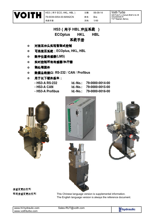
06-09-14 Bra 1/49
Voith Turbo
Voith Turbo H + L Hydraulic GmbH & Co. KG Schuckertstraße 15 71277 Rutesheim, Germany
HS3(用于 HBL 冲压系统 ) ECOplus HKL HBL
系统手册
Id.-No.: Id.-No.: Id.-No.:
79-0000-0014-00 79-0000-0015-00 79-0000-0016-00
保留变更的权利 我司保留变更的权利
This Chinese language version is supplemental information. The English language version is always the reference document.
目录
1. 修改记录 .............................................................................................................................................. 4 2. 总说明.................................................................................................................................................. 4 3. 概要 ..................................................................................................................................................... 5
日本尤尼帕斯F381A称重仪表中文资料
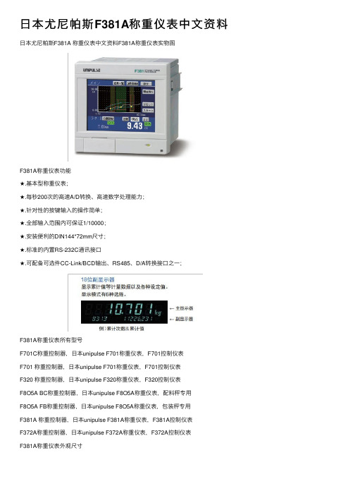
⽇本尤尼帕斯F381A称重仪表中⽂资料⽇本尤尼帕斯F381A 称重仪表中⽂资料F381A称重仪表实物图
F381A称重仪表功能
★.基本型称重仪表;
★.每秒200次的⾼速A/D转换、⾼速数字处理能⼒;
★.针对性的按键输⼊的操作简单;
★.全部输⼊范围内可保证1/10000;
★.安装便利的DIN144*72mm尺⼨;
★.标准的内置RS-232C通讯接⼝
★.可配备可选件CC-Link/BCD输出、RS485、D/A转换接⼝之⼀;
F381A称重仪表所有型号
F701C称重控制器,⽇本unipulse F701称重仪表,F701控制仪表
F701 称重控制器,⽇本unipulse F701称重仪表,F701控制仪表
F320 称重控制器,⽇本unipulse F320称重仪表,F320控制仪表
F8O5A BC称重控制器,⽇本unipulse F8O5A称重仪表,配料秤专⽤
F8O5A FB称重控制器,⽇本unipulse F8O5A称重仪表,包装秤专⽤
F381A 称重控制器,⽇本unipulse F381A称重仪表,F381A控制仪表
F372A称重控制器,⽇本unipulse F372A称重仪表,F372A控制仪表
F381A称重仪表外观尺⼨
F701称重仪表技术参数
F701称重仪表性能。
- 1、下载文档前请自行甄别文档内容的完整性,平台不提供额外的编辑、内容补充、找答案等附加服务。
- 2、"仅部分预览"的文档,不可在线预览部分如存在完整性等问题,可反馈申请退款(可完整预览的文档不适用该条件!)。
- 3、如文档侵犯您的权益,请联系客服反馈,我们会尽快为您处理(人工客服工作时间:9:00-18:30)。
Surface Mount PIN Diodes in SOT-323 (SC-70 3-Lead) Technical DataFeatures•Diodes Optimized for:Low Current SwitchingLow Distortion AttenuatingUltra-Low Distortion Switching Microwave FrequencyOperation•Surface Mount SOT-323 (SC-70)PackageSingle and Pair VersionsTape and Reel OptionsAvailable•Low Failure in Time (FIT) Rate** For more information see the Surface Mount PIN Reliability Data Sheet.Package Lead CodeIdentification(Top View)Description/ApplicationsThe HSMP-381B/C/E/F series isspecifically designed for lowdistortion attenuator applications.The HSMP-386B/C/E/F series is ageneral purpose PIN diodedesigned for low current attenua-tors and low cost switches. TheHSMP-389B/C/E/F series isoptimized for switching applica-tions where low resistance at lowcurrent, and low capacitance arerequired.The HSMP-48XB series is specialproducts featuring ultra lowparasitic inductance in the SOT-323 package, specifically designedfor use at frequencies which aremuch higher than the upper limitfor conventional SOT-323 PINdiodes. The HSMP-481B diode is alow distortion attenuating PINdesigned for operation to 3 GHz.The HSMP-482B diode is ideal forlimiting and low inductanceswitching applications up to1.5GHz. The HSMP-489B isoptimized for low current switch-ing applications up to 3 GHz.COMMONCOMMONHSMP-381B/C/E/FHSMP-386B/C/E/FHSMP-389B/C/E/FHSMP-481B, -482B, -489BAbsolute Maximum Ratings[1], TC= + 25°CSymbol Parameter Unit Absolute Maximum I f Forward Current (1 µs Pulse)Amp1P iv Peak Inverse Voltage V Same as VBRTJJunction Temperature°C150TSTGStorage Temperature°C-65 to 150θjc Thermal Resistance[2]°C/W300 Notes:1.Operation in excess of any one of these conditions may result inpermanent damage to the device.2.T C = 25°C, where T C is defined to be the temperature at the packagepins where contact is made to the circuit board.2Electrical Specifications, T C = +25°C, each diodePIN Attenuator DiodesMinimum Maximum Maximum Minimum Maximum Part PackageBreakdown Total Total High Low Number Marking LeadVoltage Resistance Capacitance Resistance Resistance HSMP-Code [1]Code Configuration V BR (V)R T (Ω)C T (pF)R H (Ω)R L (Ω)381B E0B Single 1003.00.35150010381C E2C Series381E E3E Common Anode 381FE4FCommon CathodeTest ConditionsV R = V BR I F = 100 mA V R = 50 V I R = 0.01 mA I F = 20 mA Measure f = 100 MHz f = 1 MHz f = 100 MHz f = 100 MHzI R ≤ 10 µAPIN General Purpose DiodesMinimum Typical Typical Part Package Breakdown Total Total Number Marking Lead Voltage Resistance Capacitance HSMP-Code [1]Code Configuration V BR (V)R T (Ω)C T (pF)386B L0B Single 503.01.5*0.20386C L2C Series386E L3E Common Anode 386FL4FCommon CathodeTest ConditionsV R = V BR I F = 10 mA V R = 50 V Measure f = 100 MHz f = 1 MHzI R ≤ 10 µA I F = 100 mA*PIN Switching DiodesMinimum Maximum Maximum Part Package Breakdown Total Total Number Marking Lead Voltage Resistance Capacitance HSMP-Code [1]Code Configuration V BR (V)R T (Ω)C T (pF)389B G0B Single 1002.50.30389C G2C Series389E G3E Common Anode 389F G4FCommon CathodeTest ConditionsV R = V BR I F = 5 mA V R = 5 V Measure f = 100 MHz f = 1 MHzI R ≤ 10 µA3Electrical Specifications, T C = +25°C, each diode, continued High Frequency (Low Inductance, 500MHz–3GHz PIN DiodesMinimum Maximum Typical Maximum TypicalPart Package Breakdown Series Total Total Total Number Marking Voltage Resistance Capacitance Capacitance Inductance HSMP-Code Configuration V BR (V)R S (Ω)C T (pF)C T (pF)L T (nH)Application 481B EB Dual Cathode 100 3.00.350.4 1.0Attenuator 482B FA Dual Anode 500.6*0.75* 1.0 1.0*Limiter 489BGADual Anode1002.5**0.33**0.375* 1.0SwitchTest Conditions V R = V BR I F = 100 mA V R = 50V V R = 50V f=500 MHz– MeasureI F = 10 mA* f = 1 MHz f = 1 MHz 3 GHz I R ≤ 10 µAI F = 5 mA**V R = 20V*V R = 5V*V R = 20V*V R = 5V**Typical ParametersPart Number Total Resistance Carrier LifetimeReverse Recovery TimeTotal CapacitanceHSMP-R T (Ω)τ (ns)T rr (ns)(pF)381A Series 7515003000.27386A Series 22500800.20389A Series 3.8200*——Test ConditionsI F = 1 mA I F = 50 mA V R = 10 V 50 Vf = 100 MHzT R = 250 mA I F = 20 mA I F = 10 mA*90% RecoveryI R = 6 mA*Note:1.Package marking code is laser marked.4Typical Performance, T C = 25°CFigure 2. RF Capacitance vs. Reverse Bias, HSMP-386B/C/E/F Series.0.150.300.250.200.350.400.4502641012816141820T O T A L C A P A C I T A N C E (p F )REVERSE VOLTAGE (V)Figure 1. RF Capacitance vs. Reverse Bias, HSMP-381B/C/E/F Series.0.150.300.250.200.35T O T A L C A P A C I T A N C E (p F )REVERSE VOLTAGE (V)R F R E S I S T A N C E (O H M S )I F – FORWARD BIAS CURRENT (mA)0.010.1110100Figure 3. Total RF Resistance at 25° C vs. Forward Bias Current.10000 1000100101.0T O T A L R F R E S I S T A N C E (O H M S )0.010.1110100I F – FORWARD BIAS CURRENT (mA)Figure 4. RF Resistance vs. Forward Bias Current for HSMP-381B/C/E/F Series and HSMP-481B.V R – REVERSE VOLTAGE (V)C T – C A P A C I T A N C E (p F )Figure 5. Capacitance vs. Reverse Voltage at 1 MHz.120110 100 90 80 70 60 50 40100010010DIODE RF RESISTANCE (OHMS)Figure 6. 2nd Harmonic Input Intercept Point vs. Diode RFResistance for Attenuator Diodes.I N P U T I N T E R C E P T P O I N T (d B m )11030I F – FORWARD BIAS CURRENT (mA)Figure 7. 2nd Harmonic Input Intercept Point vs. Forward Bias Current for Switch Diodes.I N P U T I N T E R C E P T P O I N T (d B m )100010010102030T r r - R E V E R S E R E C O V E R Y T I M E (n S )FORWARD CURRENT (mA)Figure 9. Reverse Recovery Time vs. Forward Current for Various Reverse Voltages. HSMP-386B/C/E/F Series.V R = 5VV R = 10V V R = 20VFORWARD CURRENT (mA)Figure 8. Reverse Recovery Time vs. Forward Current for Various Reverse Voltages. HSMP-482B.T r r – R E V E R S E R E C O V E R Y T I M E (n s )110100102030V R = 2V V R = 5VV R = 10V5Typical Performance, T C = 25°C0.20.40.60.81.01.2I F – F O R W A R D C U R R E N T (m A )V F – FORWARD VOLTAGE (mA)Figure 11. Forward Current vs.Forward Voltage. HSMP-381B/C/E/F Series and HSMP-481B.1001010.10.01I F – F O R W A R D C U R R E N T (m A )V F – FORWARD VOLTAGE (V)Figure 13. Forward Current vs.Forward Voltage. HSMP-386B/C/E/F Series.0.20.40.60.81.01.2I F – F O R W A R D C U R R E N T (m A )V F – FORWARD VOLTAGE (V)Figure 14. Forward Current vs.Forward Voltage. HSMP-389B/C/E/F Series and HSMP-489B.1001010.10.010.20.40.60.81.01.2I F – F O R W A R D C U R R E N T (m A )V F – FORWARD VOLTAGE (mA)Figure 12. Forward Current vs. Forward Voltage. HSMP-482B.T r r – R E V E R S E R E C O V E R Y T I M E (n S )FORWARD CURRENT (mA)Figure 10. Typical Reverse Recovery Time vs. Reverse Voltage. HSMP-389B/C/E/F Series.6 Typical Applications for Multiple Diode ProductsRF COMMONRF 1BIASRF 2Figure 15. Simple SPDT Switch, Using Only PositiveBias Current.Figure 16. High Isolation SPDT Switch.RF 1RF COMMONRF 1RF 2Figure 17. SPDT Switch Using Both Positive andNegative Bias Current.Figure 18. Very High Isolation SPDT Switch.RF COMMONRF 2RF 17Typical Applications for Multiple Diode Products (continued)INPUTFigure 19. Four Diode π Attenuator.Figure 20. High Isolation SPST Switch (Repeat Cells as Required).VOLTAGEBIAS8Figure 21. Internal Connections.HSMP-489BHSMP-481BTypical Applications for HSMP-48XX Low Inductance SeriesFigure 22. Circuit Layout.Microstrip Series Connection for HSMP-48XB SeriesIn order to take full advantage of the low inductance of theHSMP-48XB series when using them in series applications, both lead 1 and lead 2 should beconnected together, as shown inFigure 21.Microstrip Shunt Connections for HSMP-48XB SeriesIn Figure 23, the center conductor of the microstrip line is inter-rupted and leads 1 and 2 of the HSMP-48XB series diode are placed across the resulting gap.This forces the 0.5 nH lead induc-tance of leads 1 and 2 to appear as part of a low pass filter, reducing the shunt parasitic inductance and increasing the maximum available attenuation. The 0.3 nH of shunt inductance external to the diode is created by the via holes, and is a good estimate for 0.032" thick material.Figure 23. Circuit Layout.GROUND BY TWOVIA HOLES*0.8 pF TYPICAL FOR HSMP-482BFigure 24. Equivalent Circuit.9Figure 25. Circuit Layout.Co-Planar Waveguide Shunt Connection for HSMP-48XB SeriesCo-Planar waveguide, with ground on the top side of the printed circuit board, is shown inFigure 25. Since it eliminates the need for via holes to ground, it offers lower shunt parasiticinductance and higher maximum attenuation when compared to amicrostrip circuit.Typical Applications for HSMP-48XX Low Inductance Series (continued)*0.8 pF TYPICAL FOR HSMP-482BFigure 26. Equivalent Circuit.10Assembly Information SOT-323 PCB FootprintA recommended PCB pad layout for the miniature SOT-323 (SC-70) package is shown in Figure 27 (dimensions are in inches). This layout provides ample allowance for package placement by auto-mated assembly equipment without adding parasitics that could impair performance.Figure 27. PCB Pad Layout (dimensions in inches).SMT AssemblyReliable assembly of surfacemount components is a complexprocess that involves manymaterial, process, and equipmentfactors, including: method ofheating (e.g., IR or vapor phasereflow, wave soldering, etc.)circuit board material, conductorthickness and pattern, type ofsolder alloy, and the thermalconductivity and thermal mass ofcomponents. Components with alow mass, such as the SOT-323package, will reach solder reflowtemperatures faster than thosewith a greater mass.HP’s SOT-323 diodes have beenqualified to the time-temperatureprofile shown in Figure 28. Thisprofile is representative of an IRreflow type of surface mountassembly process.After ramping up from roomtemperature, the circuit boardwith components attached to it(held in place with solder paste)passes through one or morepreheat zones. The preheat zonesincrease the temperature of theboard and components to preventthermal shock and begin evaporat-ing solvents from the solder paste.The reflow zone briefly elevatesthe temperature sufficiently toproduce a reflow of the solder.The rates of change of tempera-ture for the ramp-up and cool-down zones are chosen to be lowenough to not cause deformationof the board or damage to compo-nents due to thermal shock. Themaximum temperature in thereflow zone (T MAX) should notexceed 235 °C.These parameters are typical for asurface mount assembly processfor HP SOT-323 diodes. As ageneral guideline, the circuitboard and components should beexposed only to the minimumtemperatures and times necessaryto achieve a uniform reflow ofsolder.TIME (seconds)TEMPERATURE(°C)5010015020025060120180240300 Figure 28. Surface Mount Assembly Profile.11Device OrientationUSER FEEDEND VIEWTOP VIEW Note: “##” represents Package Marking Code.Tape DimensionsFor Outline SOT-323 (SC-70 3 Lead)(COVER TAPE THICKNESS)DESCRIPTIONSYMBOL SIZE (mm)SIZE (INCHES)LENGTH WIDTH DEPTH PITCHBOTTOM HOLE DIAMETER A 0B 0K 0P D 1 2.24 ± 0.102.34 ± 0.101.22 ± 0.104.00 ± 0.101.00 + 0.250.088 ± 0.0040.092 ± 0.0040.048 ± 0.0040.157 ± 0.0040.039 + 0.010CAVITYDIAMETER PITCH POSITION D P 0E 1.55 ± 0.054.00 ± 0.101.75 ± 0.100.061 ± 0.0020.157 ± 0.0040.069 ± 0.004PERFORATIONWIDTHTHICKNESS W t 18.00 ± 0.300.255 ± 0.0130.315 ± 0.0120.010 ± 0.0005CARRIER TAPE CAVITY TO PERFORATION (WIDTH DIRECTION)CAVITY TO PERFORATION (LENGTH DIRECTION)F P 23.50 ± 0.052.00 ± 0.050.138 ± 0.0020.079 ± 0.002DISTANCEWIDTHTAPE THICKNESSC T t 5.4 ± 0.100.062 ± 0.0010.205 ± 0.0040.0025 ± 0.00004COVER TAPE/go/rfFor technical assistance or the location of your nearest Hewlett-Packard sales office,distributor or representative call:Americas/Canada: 1-800-235-0312 or 408-654-8675Far East/Australasia: Call your local HP sales office.Japan: (81 3) 3335-8152Europe: Call your local HP sales office.Data subject to change.Copyright © 1998 Hewlett-Packard Co.Obsoletes 5966-2323EPrinted in U.S.A. 5967-6070E (5/98)0.10 (0.004)0.425 (0.017)DIMENSIONS ARE IN MILLIMETERS (INCHES)Package DimensionsOutline SOT-323 (SC-70)Package CharacteristicsLead Material........................................................................................Copper Lead Finish.............................................................................Tin-Lead 85/15%Maximum Soldering Temperature...............................260°C for 5 seconds Minimum Lead Strength...........................................................2 pounds pull Typical Package Inductance ...................................................................2 nH Typical Package Capacitance ..............................0.08 pF (opposite leads)Option – BLK = Bulk, 100 pcs. per antistatic bagOption – TR1 = Tape and Reel, 3000 devices per 7" reelConforms to Electronic Industries RS-481, “Taping of Surface Mounted Components for Automated Placement.” Standard Quantity is 3,000Devices per Reel.Ordering InformationSpecify part number followed by option. For example:HSMP-38XA – XXXBulk or Tape and Reel Option Part Number Surface Mount PIN Hewlett-Packard。