MB15F02SLPFV1中文资料
M-15S-说明书

──
96.80
MBE058F03
当按住 F 键不放,为快速后退 目标值:右边会显示─ ─ 现在值:会快速减少数值 ※注:按 8 或 9 键为
前进/后退慢速(依机器性能而定)
3
单动模式
功能说明:在单动模式下可执行自动定位。 例 如:目前 M15 现在值显示 100.00mm,要到达目标值 200.00mm,设定步骤如下:
控制器规格
1、外观尺寸:115w × 115h × 73d (mm) 2、开孔尺寸:93w × 108h (mm) 3、安装孔位:M3 × 4 104 × 104 (mm) 4、供应电压:24 VDC 50mA 2 号 1.5V 电池 × 1 5、电池电压控制:有低电压警示 6、读头讯号线:标准:3m 7、热膨胀系数:α = 16 × 10-6 × 1/K 8、读头间隔:max. 2.5mm 9、显示屏幕:15mm LED × 6 digits × 2 line 10、输出:4 digital output(AC250V / 7A;DC24V/10A) 11、输入:4 digital input(24VDC) 12、操作组件:20 个按键 13、Test mark/interfer.Protection class:3 accord. to IEC 801 14、速度:1.5m/s 15、系统精度:± (0.025+0.02L)mm (L: 米) 16、重现性:0.01mm 17、温度:工作温度 0 + 50℃;储存温度 –20 +70℃ 18、湿度:max. 95% rF(Condensation not permitted)
表示 LED 灯亮闪烁
MB15E05SRPV1资料
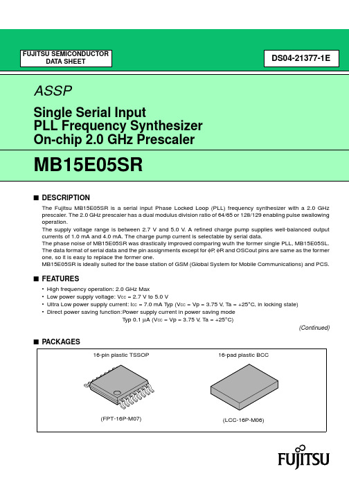
DS04-21377-1EFUJITSU SEMICONDUCTORDATA SHEETASSPSingle Serial InputPLL Frequency Synthesizer On-chip 2.0 GHz PrescalerMB15E05SRs DESCRIPTIONThe Fujitsu MB15E05SR is a serial input Phase Locked Loop (PLL) frequency synthesizer with a 2.0 GHz prescaler. The 2.0 GHz prescaler has a dual modulus division ratio of 64/65 or 128/129 enabling pulse swallowing operation.The supply voltage range is between 2.7 V and 5.0 V . A refined charge pump supplies well-balanced output currents of 1.0 mA and 4.0 mA. The charge pump current is selectable by serial data.The phase noise of MB15E05SR was drastically improved comparing wuth the former single PLL, MB15E05SL.The data format of serial data and the pin assignments except for φP , φR and OSCout pins are same as the former one, so it is easy to replace the former one.MB15E05SR is ideally suited for the base station of GSM (Global System for Mobile Communications) and PCS.s FEATURES•High frequency operation: 2.0 GHz Max•Low power supply voltage: V CC = 2.7 V to 5.0 V•Ultra Low power supply current:I CC = 7.0 mA T yp (V CC = Vp = 3.75 V , T a = +25°C, in locking state)•Direct power saving function:Power supply current in power saving modeT yp 0.1 µA (V CC = Vp = 3.75 V , T a = +25°C)(Continued)s PACKAGESMB15E05SR2(Continued)•Dual modulus prescaler: 64/65 or 128/129•Serial input 14-bit programmable reference divider: R = 3 to 16,383•Serial input programmable divider consisting of:- Binary 7-bit swallow counter: 0 to 127- Binary 11-bit programmable counter: 3 to 2,047•Software selectable charge pump current•On-chip phase control for phase comparator•Built-in digital locking detector circuit to detect PLL locking and unlocking.•Operating temperature: T a = –40 °C to +85 °Cs PIN ASSIGNMENTSMB15E05SR3s PIN DESCRIPTIONSPin no.Pin name I/O DescriptionsTSSOP BCC 116OSC IN I Programmable reference divider input. Connection to a TCXO.21N.C.–No connection.32V P –Power supply voltage input for the charge pump.43V CC –Power supply voltage input.54D O O Charge pump output.Phase of the charge pump can be selected via programming of the FC bit.65GND –Ground.76Xfin I Prescaler complementary input, which should be grounded via a capacitor.87fin I Prescaler input.Connection to an external VCO should be done via AC coupling.98Clock I Clock input for the 19-bit shift register.Data is shifted into the shift register on the rising edge of the clock.(Open is prohibited.)109Data I Serial data input using binary code.The last bit of the data is a control bit. (Open is prohibited.)1110LEILoad enable signal input. (Open is prohibited.)When LE is set high, the data in the shift register is transferred to a latch according to the control bit in the serial data.1211PS I Power saving mode control. This pin must be set at “L” at Power-ON.(Open is prohibited.)PS = “H”; Normal modePS = “L”; Power saving mode 1312N.C.–No connection.1413LD/fout O Lock detect signal output (LD)/phase comparator monitoring output (fout).The output signal is selected via programming of the LDS bit.LDS = “H”; outputs fout (fr/fp monitoring output)LDS = “L”; outputs LD (“H” at locking, “L” at unlocking.)1514N.C.–No connection.1615N.C.–No connection.MB15E05SR4s BLOCK DIAGRAMMB15E05SR5s ABSOLUTE MAXIMUM RATINGSWARNING:Semiconductor devices can be permanently damaged by application of stress (voltage, current,temperature, etc.) in excess of absolute maximum ratings. Do not exceed these ratings.s RECOMMENDED OPERATING CONDITIONSWARNING:The recommended operating conditions are required in order to ensure the normal operation of thesemiconductor device. All of the device’s electrical characteristics are warranted when the device is operated within these ranges.Always use semiconductor devices within their recommended operating condition ranges. Operation outside these ranges may adversely affect reliability and could result in device failure.No warranty is made with respect to uses, operating conditions, or combinations not represented on the data sheet. Users considering application outside the listed conditions are advised to contact their FUJITSU representatives beforehand.ParameterSymbol ConditionRating Unit RemarkMin Max Power supply voltage V CC ––0.5 5.5V V P –V CC 6.0V Input voltage V I ––0.5V CC +0.5V Output voltage V O Except DoGND V CC V V O Do GND V P V Storage temperatureTstg––55+125°CParameterSymbol ValueUnit RemarkMin Typ Max Power supply voltage V CC 2.7 3.75 5.0V V P V CC – 5.5V Input voltageV I GND –V CC V Operating temperatureTa–40–+85°CMB15E05SR6s ELECTRICAL CHARACTERISTICS(V CC = 2.7 V to 5.0 V, T a = –40 °C to +85 °C)*1: Conditions; fosc = 13 MHz, Vosc = 1.2 V PP, T a = +25°C, in locking state.*2: V CC = V P = 3.75 V, fosc = 13 MHz, Vosc = 1.2 V PP, T a = +25°C, in power saving mode*3: AC coupling. 1000 pF capacitor is connected under the condition of min. operating frequency.*4: The symbol “–” (minus) means direction of current flow.*5: V CC = V P = 3.75 V, T a = +25°C (||I3| – |I4||) / [(|I3| + |I4|) /2] × 100(%)(Continued) Parameter Symbol ConditionValueUnitMin Typ MaxPower supply current*1I CC fin = 2000 MHz, V CC = V P = 3.75 V–7.0–mA Power saving current I PS PS = “L”–0.1*220µA Operating frequencyfin f IN–300–2000MHzOSC IN fosc–3–40MHz Input sensitivityfin*3Pfin50 Ω system(Refer to the measurementcircuit.)–15–+2dBm OSC IN*3V OSC–0.5–V CC Vp-p“H” level input voltage Data,Clock,LE, PSV IH–V CC × 0.7––V “L” level input voltage V IL–––V CC × 0.3“H” level input current Data,Clock,LE, PSI IH*4––1.0–+1.0µA “L” level input current I IL*4––1.0–+1.0“H” level input currentOSC INI IH–0–+100µA “L” level input current I IL*4––100–0“H” level output voltageLD/foutV OH V CC = V P = 3.75 V, I OH = –1 mA V CC – 0.4––V “L” level output voltage V OL V CC = V P = 3.75 V, I OL = 1 mA––0.4“H” level output voltageDoV DOH V CC = V P = 3.75 V, I DOH = –0.5 mA V P – 0.4––V “L” level output voltage V DOL V CC = V P = 3.75 V, I DOL = 0.5 mA––0.4High impedance cutoffcurrent Do I OFFV CC = V P = 3.75 V,V OFF = 0.5 V to V P – 0.5 V–– 2.5nA“H” level output currentLD/foutI OH V CC = V P = 3.75 V–––1.0mA “L” level output current I OL V CC = V P = 3.75 V 1.0––“H” level output currentDoI DOH*4V CC = 3.75 V,V P = 3.75 V,V DO = V P/2,Ta = +25°CCS bit = “1”––4.0–mACS bit = “0”––1.0–“L” level output current I DOLCS bit = “1”– 4.0–CS bit = “0”– 1.0–Charge pump currentrateI DOL/I DOH I DOMT*5V DO = V P/2–5–%vs V DO I DOVD*60.5 V ≤ V DO≤ V P – 0.7 V–10–%vs Ta I DOTA*7– 40°C ≤ Ta ≤ +85°C, V DO = V P/2–3–%MB15E05SR(Continued)*6: V CC = V P = 3.75 V, T a = +25°C [(||I2| – |I1||) /2] / [(|I1| + |I2|) /2] × 100(%) (Applied to each I DOL, I DOH)*7: V CC = V P = 3.75 V, V DO = V P/2 (||I DO(+85°C)| – |I DO(–40°C)| |/2) / (|I DO(+85°C)| + |I DO(–40°C)| /2) × 100(%) (Applied to each I DOL, I DOH)7MB15E05SR8s FUNCTIONAL DESCRIPTION1.Pulse Swallow FunctionThe divide ratio can be calculated using the following equation:f VCO = [(P× N) + A] × f OSC÷ R (A < N)f VCO:Output frequency of external voltage controlled oscillator (VCO)N:Preset divide ratio of binary 11-bit programmable counter (3 to 2,047)A:Preset divide ratio of binary 7-bit swallow counter (0 ≤ A ≤ 127)f OSC:Output frequency of the reference frequency oscillatorR:Preset divide ratio of binary 14-bit programmable reference counter (3 to 16,383)P:Preset divide ratio of modulus prescaler (64 or 128)2.Serial Data InputSerial data is processed using the Data, Clock, and LE pins. Serial data controls the programmable reference divider and the programmable divider separately.Binary serial data is entered through the Data pin.One bit of data is shifted into the shift register on the rising edge of the Clock. When the LE signal pin is taken high, stored data is latched according to the control bit data as follows:Table 1. Control Bit(1) Shift Register ConfigurationControl bit (CNT)Destination of serial dataH For the programmable reference dividerL For the programmable divider12345678910111213141516171819 CNT R1R2R3R4R5R6R7R8R9R10R11R12R13R14SW FC LDS CS Programmable Reference CounterMSBData FlowCNT: Control bit[T able 1]R1 to R14: Divide ratio setting bit for the programmable reference counter (3 to 16,383)[T able 2]SW: Divide ratio setting bit for the prescaler (64/65 or 128/129)[T able 5]FC: Phase control bit for the phase comparator[T able 8]LDS: LD/f OUT signal select bit[T able 7]CS: Charge pump current select bit[T able 6]Note: Start data input with MSB first.LSBMB15E05SR9Table 2. Binary 14-bit Programmable Reference Counter Data SettingNote : Divide ratio less than 3 is prohibited.Table 3. Binary 11-bit Programmable Counter Data SettingNote : Divide ratio less than 3 is prohibited.Divide ratio(R)R14R13R12R11R10R9R8R7R6R5R4R3R2R1300000000000011400000000000100⋅⋅⋅⋅⋅⋅⋅⋅⋅⋅⋅⋅⋅⋅⋅1638311111111111111Divide ratio(N)N11N10N9N8N7N6N5N4N3N2N1300000000011400000000100⋅⋅⋅⋅⋅⋅⋅⋅⋅⋅⋅⋅20471111111111112345678910111213141516171819CNTA1A2A3A4A5A6A7N1N2N3N4N5N6N7N8N9N10N11Programmable Counter LSB MSBData Flow CNT : Control bit[T able 1]N1 to N11: Divide ratio setting bits for the programmable counter (3 to 2,047)[T able 3]A1 to A7: Divide ratio setting bits for the swallow counter (0 to 127)[T able 4]Note: Data input with MSB first.MB15E05SR10Table 4. Binary 7-bit Swallow Counter Data SettingTable 5. Prescaler Data SettingTable 6. Charge Pump Current SettingTable 7. LD/fout Output Select Data Setting(2) Relation between the FC Input and Phase CharacteristicsThe FC bit changes the phase characteristics of the phase comparator. The internal charge pump output level (D O) is reversed according to the FC bit. Also, the monitor pin (fout) output is controlled by the FC bit. The relationship between the FC bit and D O is shown below.Table 8. FC Bit Data Setting (LDS = “1”)*: High impedanceDivide ratio(A)A7A6A5A4A3A2A10000000010000001⋅⋅⋅⋅⋅⋅⋅⋅1271111111SW Prescaler divide ratio164/650128/129CS Current value1±4.0 mA0±1.0 mALDS LD/fout output signal1fout signal0LD signalFC = 1FC = 0D O LD/fout D O LD/foutfr > f P Hfout = frLfout = fpfr < f P L Hfr = f P Z*Z*When designing a synthesizer, the FC pin setting depends on the VCO and LPF characteristics.3. Power Saving Mode (Intermittent Mode Control Circuit)Table 10. PS Pin SettingPS pin StatusH Normal modeL Power saving modeThe intermittent mode control circuit reduces the PLL power consumption.By setting the PS pin low, the device enters into the power saving mode, reducing the current consumption. See the Electrical Characteristics chart for the specific value.The phase detector output, Do, becomes high impedance.For the signal PLL, the lock detector, LD, remains high, indicating a locked condition.Setting the PS pin high, releases the power saving mode, and the device works normally.The intermittent mode control circuit also ensures a smooth startup when the device returns to normal operation. When the PLL is returned to normal operation, the phase comparator output signal is unpredictable. This is because of the unknown relationship between the comparison frequency (fp) and the reference frequency (fr) which can cause a major change in the comparator output, resulting in a VCO frequency jump and an increase in lockup time. T o prevent a major VCO frequency jump, the intermittent mode control circuit limits the magnitude of the error signal from the phase detector when it returns to normal operation.Notes : •When power (V CC) is first applied, the device must be in standby mode, PS = Low.•The serial data input after the power supply becomes stable and the the power saving mode is released after completed the data input..s SERIAL DATA INPUT TIMINGs PHASE COMPARATOR OUTPUT WAVEFORMs MEASURMENT CIRCUIT (for Measuring Input Sensitivity fin/OSC IN)s TYPICAL CHARACTERISTICS4.fin input impedance5.OSC IN input impedances REFERENCE INFORMATION(Continued)MB15E05SR s APPLICATION EXAMPLEs USAGE PRECAUTIONST o protect against damage by electrostatic discharge, note the following handling precautions:-Store and transport devices in conductive containers.-Use properly grounded workstations, tools, and equipment.-T urn off power before inserting device into or removing device from a socket.-Protect leads with a conductive sheet when transporting a board-mounted device.21MB15E05SR22s ORDERING INFORMATIONPart number Package RemarksMB15E05SRPFT16-pin, Plastic TSSOP(FPT-16P-M07)MB15E05SRPV116-pad, Plastic BCC(LCC-16P-M06)MB15E05SR s PACKAGE DIMENSIONS(Continued)2324FUJITSU LIMITEDAll Rights Reserved.The contents of this document are subject to change without notice. Customers are advised to consult with FUJITSU sales representatives before ordering.The information, such as descriptions of function and application circuit examples, in this document are presented solely for the purpose of reference to show examples of operations and uses of Fujitsu semiconductor device; Fujitsu does not warrant proper operation of the device with respect to use based on such information. When you develop equipment incorporating the device based on such information, you must assume any responsibility arising out of such use of the information. Fujitsu assumes no liability for any damages whatsoever arising out of the use of the information.Any information in this document, including descriptions of function and schematic diagrams, shall not be construed as license of the use or exercise of any intellectual property right, such as patent right or copyright, or any other right of Fujitsu or any third party or does Fujitsu warrant non-infringement of any third-party’s intellectual property right or other right by using such information. Fujitsu assumes no liability for any infringement of the intellectual property rights or other rights of third parties which would result from the use of information contained herein.The products described in this document are designed, developed and manufactured as contemplated for general use, including without limitation, ordinary industrial use, general office use, personal use, and household use, but are not designed, developed and manufactured as contemplated (1) for use accompanying fatal risks or dangers that, unless extremely high safety is secured, could have a serious effect to the public, and could lead directly to death, personal injury, severe physical damage or other loss (i.e., nuclear reaction control in nuclear facility, aircraft flight control, air traffic control, mass transport control, medical life support system, missile launch control in weapon system), or (2) for use requiring extremely high reliability (i.e., submersible repeater and artificial satellite).Please note that Fujitsu will not be liable against you and/or any third party for any claims or damages arising in connection with above-mentioned uses of the products.Any semiconductor devices have an inherent chance of failure. You must protect against injury, damage or loss from such failures by incorporating safety design measures into your facility and equipment such as redundancy, fire protection, and prevention of over-current levels and other abnormal operating conditions.If any products described in this document represent goods or technologies subject to certain restrictions on export under the Foreign Exchange and Foreign Trade Law of Japan, the prior authorization by Japanese government will be required for export of those products from Japan.F0310©FUJITSU LIMITED Printed in Japan。
海利普变频器产品说明书

海利普企业简介营销服务网络图*图注红:销售服务中心蓝:办事处浙江海利普电子科技有限公司成立于2001年,于2005年纳入Danfoss旗下,成为其全资子公司。
丹佛斯是丹麦最大的跨国工业制造公司,创立于 1933年,丹佛斯以推广应用先进的制造技术,并关注节能环保而闻名于世,是制冷和空调控制,供热和水控制,以及传动控制等领域处于世界领先地位的产品制造商和服务供应商。
在过去的10年中,海利普经历了巨大的变化,已发展成一家集研发、生产、销售于一体的国家级高新技术企业,同时也是国内唯一一家拥有省级变频研发中心的企业。
海利普是目前中国最大的变频器生产厂家,其核心产品HLP系列变频器,广泛应用于起重、纺织、印染 、石油、化工、建筑、建材、橡胶、塑料、包装、印刷、造纸、食品、饮料、环保、水处理、机床等行业,先后被列入“国家重点新产品”、 “国家火炬计划项目”,并于2004年被授于“浙江省名牌产品”、“国内最具有竞争力的产品”。
为了适应丹佛斯在中国建立第二家乡市场的战略,海利普依靠丹佛斯的强大支持,寻求高速发展,更加巩固了海利普在中国变频器领域的领先地位,同时逐渐成为丹佛斯旗下的能源电子部在亚太地区的制造和物流中心。
公司愿景:比市场增长更快,成为中国市场品质最高的知名品牌。
目录通用型变频器HLP-A通用型变频器 / 4HLP-C+迷你型变频器 / 12矢量型变频器HLP-B高性能矢量型变频器/ 17HLP-NV矢量型变频器 / 24专用型变频器HLP-P风机/水泵专用变频器 / 30 HLP-H中频机 / 36HLP-F纺织专用变频器 / 40HLP-J注塑机专用变频器 / 43HLP-CP跑步机/手套机专用变频器 / 47 HLP-M机床专用变频器 / 51常用选配件直流电抗器 / 55交流输入/输出电抗器 / 55输入/输出滤波器 / 57制动单元与制动电阻 / 57接线用断路器及漏电开关 / 58电磁接触器及浪涌吸收器 / 59隔离变压器 / 59 海利普变频器 系列产品本产品为通用型变频器,软件功能强大,具有多种控制方式;内置PID、简易PLC;输出转矩高(150%/1分钟),过载能力强,广泛应用于编织、化纤、印染、塑料、轻工、机械、化工、钢铁、造纸等各种行业,并受到用户的一致好评。
富士施乐DocuPrint M115f多功能一体机说明书(中文)
使用手冊- 適用於單機操作 -關於這本使用手冊當閱讀操作說明時,請遵守這些指導方針:w c v&警告:請務必小心遵守,以免身體受傷。
注意:請務必遵守,以免損害設備。
請務必遵守這個禁止符號的指示,以免造成身體受傷,或是設備損壞。
附註:包含有關使用本產品的重要資訊和提示。
指示可以找到詳細說明的頁數。
2目錄重要的安全說明 (5)控制面板的說明 (6)使用液晶面板 (8)調整控制面板角度 (10)電源故障後自動重新開機 (11)處理紙張選擇紙張 (14)放入紙張 (15)放置CD/DVD (18)記憶卡的使用方法 (20)放置原稿 (22)複印複印文件 (26)複製/修複照片 (28)CD/DVD複印 (30)複印模式選單清單 (32)記憶卡列印模式列印照片 (36)使用各種版面配置列印 (38)列印CD/DVD (40)列印照片賀卡 (43)從索引頁列印照片 (47)播放影片和列印照片 (50)照片模式選單清單.............................................................52其他模式列印格線紙 (54)列印塗鴨畫 (56)掃描至記憶卡 (58)掃描至電腦 (59)備份資料至外部儲存裝置 (60)其他模式選單清單 (61)設定模式(維護)檢查墨水卡匣存量 (64)檢查和清潔印字頭 (65)校正印字頭 (67)PictBridge 設定 (69)設定模式選單清單 (71)解決方法錯誤訊息 (74)更換墨水卡匣 (75)夾紙 (78)印表機錯誤 (84)列印問題 (85)其他問題 (86)客戶技術支援服務 (86)附錄 (87)版權注意事項 (88)34重要的安全說明5控制面板的說明按鍵a Unlock調低(收起)控制面板。
b P啟動 On開啟或關閉本產品的電源。
c更改照片的檢視方式或裁切照片。
d x Menu顯示各個模式下的詳細設定。
e-液晶面板,顯示照片和選單。
MB90F562BPFM中文资料

The MB90560/565 series is a general-purpose 16-bit microcontroller designed for industrial, OA, and process control applications that require high-speed real-time processing. The device features a multi-function timer able to output a programmable waveform. The microcontroller instruction set is based on the same AT architecture as the F2MC-8L and F2MC-16L families with additional instructions for high-level languages, extended addressing modes, enhanced signed multiplication and division instructions, and a complete range of bit manipulation instructions. The microcontroller has a 32-bit accumulator for processing long word (32-bit) data.
s FEATURES
• Clock • Internal oscillator circuit and PLL clock multiplication circuit • Oscillation clock Clock speed selectable from either the machine clock, main clock, or PLL clock. The main clock is the oscillation clock divided into 2 (0.5 MHz to 8 MHz for a 1 MHz to 16 MHz base oscillation) . The PLL clock is the oscillation clock multiplied by one to four (4 MHz to 16 MHz for a 4 MHz base oscillation) . • Minimum instruction execution time : 62.5 ns (for oscillation = 4 MHz, PLL clock setting = × 4, VCC = 5.0 V) • Maximum CPU memory space : 16 MB • 24-bit addressing • Bank addressing (Continued)
BLM15HG102SN1D中文资料
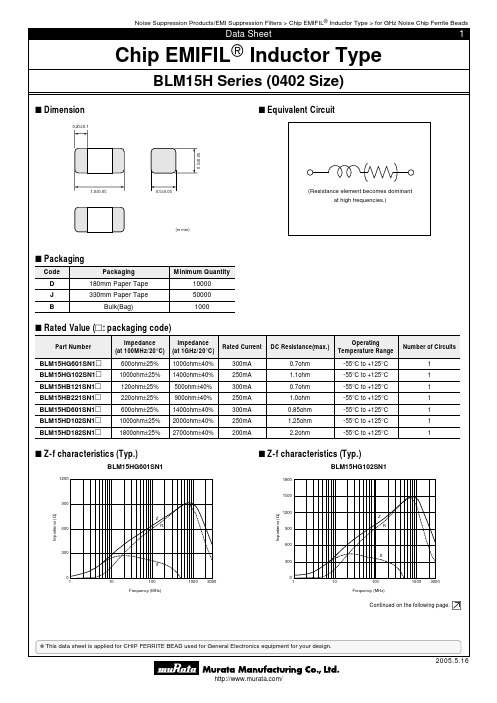
BLM15H Series (0402 Size)
I Dimension
0.25±0.1
I Equivalent Circuit
0.5±0.05
1.0±0.05
0.5±0.05
(Resistance element becomes dominant at high frequencies.)
(in mm)
800
400
0 1
Z R
X
10
100
Frequency (MHz)
1000 3000
I Z-f characteristics (Typ.)
BLM15HD182SN1
4000
I Z-f characteristics (Typ.)
BLM15HD102SN1
2500
2000
Impedance (Ω)
1500 1000
500
Z R
X
0
1
10
100
Frequency (MHz)
1000 3000
Impedance (Ω)
3000 2000 1000
Z R
X
0
1
10
100
1000 3000
Frequency (MHz)
I !Caution/Notice
!Caution (Rating) Do not use products beyond the rated current and rated voltage as this may create excessive heat and deteriorate the insulation resistance.
300mA 250mA 300mA 250mA 300mA 250mA 200mA
(整理)东方动力15MW发电机说明书.

东方动力15MW发电机说明书一、概述本说明书适用于3MW-15MF QF系列汽轮发电机,该系列发电机系三相两极交流同步发电机,经汽轮机或燃汽轮机直接耦合传动。
额定转速3000r/min,频率为50HZ,采用空气冷却密闭循环通风系统。
发电机的转向从透平机端看为顺时针方向。
型号什么:Q F×××-×-2×设计序号:A、B、C、D代表发电机为二级、额定转速:3000r/min额定功率:MW“W”为无刷励磁,无“W”为静止可控硅励磁“1”、“2”代表额定电压为6.2kV、10.5kV“B”为双支撑结构,无“B”为单支撑结构空气冷却汽轮发电机QF系列型发电机符合有关国家标准规定和本电机技术条件。
GB755—2000 旋转机定额与性能GB/T7064-2002透平同步电机技术要求GB/T7409.3-97 大型同步电机励磁系统技术条件JB/T7784-95 透平同步电机用交流励磁机技术(适用于无刷励磁)二、技术数据及允许运行方式1.本型发电机的正常使用条件:(1)海拔不超过1000m(2)空气温度不超过+40℃(3)电机周围空气不得存在酸碱性等有害电机绝缘或零部件之气体与灰尘:(4)安装在隐蔽的厂房内2.QF系列发电机与额定工况下运行时,各主要部件温升限度如下表(B级绝缘):QF系列发电机与额定工况下运行时,各主要部件温升限度如下表(F级绝缘):注:本型发动机的空气冷却器,在进水温度不超过+30℃时,开足水量保证冷却后的空气温度不超过+40℃,当水温度提高时可按提高的进风温度,相应降低发电机绕组的允许温升,此时发电机的功率,以温升不超过降低后的允许值为准。
3.奉型发电机当功率因数为额定值,其电压与额定值的偏差不超过±5%,且其频率与额定值的偏差不超过±2%情况下连续运行时,能保证输出额定功率。
当定子电压与额定值的偏差大于±5%,但不大于±10%时,允许发电机继续运行但此时定子电流及励磁电流允许值,应以发电机各部件的允许温升为限。
MB15-2M高频浪涌测试仪说明书
MB15-2M高频浪涌测试仪说明书
MB15-2M高频浪涌测试仪数字传输性能分析仪,适用于数字传输系统的工程施工、工程验收及日常维护测试。
其性能可靠稳定、功能齐全、体积小巧,采用大屏幕中文显示,操作简洁容易。
MB15-2M高频浪涌测试仪数字传输性能分析仪可对2Mbit/s接口数字通道进行测试,具有两个2Mbit/s接口,可同时对两条通道进行测试。
一、测试设置
用光标移动键将光标移到测试设置处,按ENTER进入测试设置界面,用于设置测试项目及参数。
光标移到测试设置处时也可用F键直接选择测试设置界面中的常规测试、通过测试、时延测试、音频测试、APS测试等工作方式。
二、测试结果
用光标移动键将光标移到测试结果处,按ENTER键进入测试结果界面,用于显示各种测试结果。
光标移到测试结果外时也可用F键直接选择测试结果、时隙分析、监听、 G.703模板等界面。
三、档案管理
用光标移动键将光标移到档案管理处,按ENTER进入档案管理-设置存取界面。
光标移到测试结果处时也可用F键直接选择档案管理-设置存
取界面或档案管理-结果存取界面。
四、仪表设置
用光标移动键将光标移到仪表设置处,按ENTER键进入仪表设置界面,用于设置仪表的一些辅助参数。
光标移到仪表设置处时也可用F键直接选择仪表设置界面内的子菜单或版本信息界面。
连接PC 机,用光标移动键将光标移到PC机连接处按ENTER键或F1键关闭连接PC机。
五、功能
按 F2键打开连接PC机功能,液晶显示器的状态显示区同时显示品软件升级用光标移动键将光标移到软件升级处,按ENTERF1键进入仪表内部软件升级功能说明界面。
DLT德力通产品推介说明
DLTK系列乘客电梯产品推介说明一、公司简介湖南德力通电梯有限公司是一家集电梯的研发、制造、销售、安装和维保于一体的综合性企业。
公司座落于南北重要的交通枢纽湖南株洲,水陆交通通讯十分便利。
厂区占地2.5公顷,设有现代化车间(垂直电梯及自动扶梯生产流水线)和国际先进的专业检测、机械加工设备、研发中心等;拥有一批高素质的专业技术人才。
具备年产各类垂直电梯3500台、自动扶梯1000台的生产规模。
目前本厂产品已覆盖全国二十多个省市,并在长沙、广州、深圳、泉州、桂林、扬州、合肥、成都、兰州、潍坊等地设立了办事处及售后服务网点,负责本公司产品在当地的销售及售后服务工作。
德力通电梯有限公司与一些国际著名电梯配件厂商展开全面合作,专业从事高科技、数字化电梯的研究与开发,是世界电梯无机房、无齿轮高科技应用领域内的领先者。
让"用户满意"是德力通人的无上追求,质量与信誉是公司的一贯宗旨。
在生产质量控制与安装、服务过程中严格执行ISO9001-2000与ISO14000、OHSAS18000等相关国际标准管理体系,配备有专业的安装和服务队伍,设立了24小时服务的服务热线,建立起了辐射全国的服务网络和迅捷的备品备件供应体系,为客户提供全方位的服务与支持。
我们热情欢迎宾客用户惠顾、咨询、洽谈订货。
二、产品介绍DLTK系列乘客电梯,是湖南德力通电梯有限公司推出的最新一代高科技绿色环保产品,它具有高效节能、低噪声、无(齿轮箱)油污染、无电源电网污染等优点。
一、最先进的永磁同步拖动系统DLTK系列乘客电梯,采用国际上最先进的永磁同步变频调速拖动技术。
永磁同步电机不需要无功励磁电流,定子铜耗小,功率因素高,并具有低速性、快速性、硬机械特性、停车自闭等优点。
同时,永磁同步电机正常工作时不产生谐波干扰,对电源电网无污染。
二、平稳高效的无齿轮曳引系统DLTK系列乘客电梯,采用无齿轮曳引技术,没有齿轮啮合,彻底消除了齿轮机械传动的振动和噪声,使电梯运行更加平稳,噪声大为降低。
最新丹佛斯FC51中文参数手册
目录1. 安全性3安全说明3认证3一般警告3避免意外启动4开始维修工作之前52. 简介7类型代码73. 编程9如何编程9使用 MCT-10 编程9使用 LCP 11 和 LCP 12 编程9状态菜单11快捷菜单11主菜单124. 参数说明13参数组 0:操作/显示13参数组 1:负载/电动机17参数组 2:制动26参数组 3:参考值/加减速29参数组 4:极限/警告35参数组 5:数字输入/输出38参数组 6:模拟输入/输出43参数组 7:控制器49参数组 8:通讯51参数组 13:智能逻辑56参数组 14:特殊功能64参数组 15:变频器信息67参数组 16:数据读数705. 参数列表756. 疑难解答79索引80VLT ®Micro Drive FC 51目录1. 安全性VLT® Micro Drive FC 51 11.安全性1.1.1.高压警告连接到主电源时,变频器带有危险电压。
如果电动机或变频器安装不当,可能导致设备损坏甚至人身伤亡。
因此,必须遵守本手册的说明以及国家和地方的规章和安全规定。
1.1.2.安全说明•确保变频器已正确接地。
•当变频器同电源相连时,请勿拔掉主电源插头、电动机插头或其它电源插头。
•防止用户接触供电电压。
•按照国家和地方法规进行电动机过载保护。
•接地漏电电流大于 3.5 mA。
•[OFF](停止)键不是安全开关。
它不能将变频器与主电源断开。
1.1.3.认证1.1.4.一般警告警告:即使设备已断开与主电源的连接,触碰电气部件也可能会导致生命危险。
此外还应确保其它电压输入也已经断开(直流中间电路的连接)。
请注意,即使 LED 熄灭,直流回路上也可能存在高压。
在接触 VLT Micro Drive 的任何可能带电部分之前,对于所有规格,请等待至少 4分钟的时间。
仅当特定设备的铭牌上规定了更短的等待时间,才允许更短的时间。
漏电电流VLT Micro Drive FC 51 的接地漏电电流超过 3.5 mA。
士林变频器说明书

环境 保存温度
-20 ~ +65℃
周围环境 振动
室内,无腐蚀性气体,无易燃性气体,无易燃性粉尘
2
5.9m/s (0.6G)以下,符合 JIS C0911 的标准
-2-
1-3 外形尺寸 1-3-1 SH0X0-0.75K ~3.7K (1HP ~5HP)系列
冷却风扇
AB
C
A
型号
(mm) (mm) (mm) 型号
电 电源电压容许范围
323~528V 50Hz / 60Hz
源 电源频率变动范围
±5%
电源容量 kVA
2.5
4.5
5.5
9.0
12
17
冷却方式
自冷
强制风冷
变频器消耗功率 W
50
85
100
160
230
300
(注)
变频器重量 kg
1.3
1.5
2.5
2.5
5.6
5.6
(注) 额定输出电流、额定输出容量、变频器消耗功率的测试条件︰载波频率(Pr72)为 2kHz,变 频器输出电压为 220V / 440V,输出频率为 60Hz,周围温度为 40℃。
R- S- T U-V-W P- PR
P- N
主回路板端子
说明
连接到市电电源。
连接到三相鼠笼式马达。
连接煞车电阻。
(注 1)
连接煞车单元
(注 4)
变频器的机壳接地。220V 系列为第三种接地。440V 系列为特
种接地。
(注 1) 1. SH0X0-0.75K~3.7K(1HP~5HP)系列的变频器,出厂时并没有附加煞车电阻。 2. 回生电压的相关知识,请参考第 3 章 Pr30。
MB15F78ULPFT-G-BND-EFE1;中文规格书,Datasheet资料
DS04-21369-1E
ASSP
Dual Serial Input PLL Frequency SyntheESCRIPTION
The Fujitsu MB15F78UL is a serial input Phase Locked Loop (PLL) frequency synthesizer with a 2600 MHz and a 1200 MHz prescalers. A 32/33 or a 64/65 for the 2600 MHz prescaler, and a 16/17 or a 32/33 for the 1200 MHz prescaler can be selected for the prescaler that enables pulse swallow operation. The BiCMOS process is used, as a result a supply current is typically 4.5 mA at 2.7 V. The supply voltage range is from 2.4 V to 3.6 V. A refined charge pump supplies well-balanced output current with 1.5 mA and 6 mA selectable by serial date. The data format is the same as the previous one MB15F08SL, MB15F78SP . Fast locking is achieved for adopting the new circuit. The new package (BCC20) decreases a mount area of MB15F78UL more than 30% comparing with the former BCC16 (for dual PLL) . MB15F78UL is ideally suited for wireless mobile communications, such as GSM and PCS.
MB15E07SLPFV1-G-ER-6E1;中文规格书,Datasheet资料

Clock input for the 19-bit shift register. Data is shifted into the shift register on the rising edge of the clock. (Open is prohibited.)
Ta
–40
–
+85
°C
WARNING: The recommended operating conditions are required in order to ensure the normal operation of the semiconductor device. All of the device’s electrical characteristics are warranted when the device is operated within these ranges.
(11) 12 PS
1-bit control latch
(10) 11 LE
(9) 10 Data
(8) 9 Clock
: SSOP ( ) : BCC
4 /
MB15E07SL
s ABSOLUTE MAXIMUM RATINGS
Parameter
Symbol
Condition
Phase comparator N-channel open drain output for an external charge pump. Phase can be selected via programming of the FC bit.
mb10f中文资料_数据手册_参数
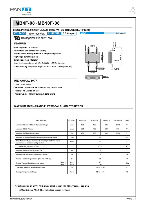
MB10F-08 UNIT
1000
V
700
V
1000
V
A
A
A2S
V
μA pF
oC/W
oC oC
Note:1.Mounted on a FR4 PCB, single-sided copper, with 100cm2 copper pad area 2.Mounted on a FR4 PCB, single-sided copper, mini pad.
(Note 1) (Note 2)
CJ
Rθ JC Rθ JA
TJ
Storage Temperature Range
TSTG
MB4F-08 400 280 400
MB6F-08
MB8F-08
600
800
420
560
600
800
0.8
30
3.735 1
5
15 25 138 -55 to +150
-55 to +150
• Panjit International Inc. disclaims any and all liability arising out of the application or use of any product including damages incidentally and consequentially occurred.
日本富士变频器功能表

F27 日本富士变频器功能表时间: 2008年10月01日 来源:溧阳电梯网 作者: 佚名 浏览次数:735 【字体:大 中 小】一、基本功能功能码 名称 LCD 画面显示 可设定范围 单位 最小单位 出厂设定 运行时变更 备注 F00 密码功能 F00 DATA PRTC 0--FFFF - - 0F01 频 率设定1 F01 FREQ CMD 1 0:键盘操作(∧∨键) 1:电压输入(端子12)(0--+10VDC)2:电流输入(端子C1)(4--20mADC)3:电压输入+电流输入(端子12+端子C1)4:用极性信号可作反向运行(端子12)(0--10VDC) - - 0 F02 运行操作 F02 OPR METHOD 0:键盘操作 FWD REV STOP 键1:外部信号(数字输入)(用 FWD REV 端子信号运行) - - 0 选择运行操作的输入方式F03 最高输出频率1 F03 MAX Hz - 1 50 - 120 Hz 1 60 可设定输出的最高频率 F04 基本频率1 F04 BASE Hz - 1 25 - 120 Hz 1 50 设定基本频率F05 额定电压1(基本频率1时) F05 RADET V - 1 0:输出与电源电压成比例的电压80 - 240: AVR 动作(200V 级)320 - 480: AVR 动作(400V 级) V 1 200V 级:200400V 级:400 设定基本频率1(F04)时的电压F06 最高输出电压1(最高输出频率时) F06 MAX V - 1 80 - 240V: AVR 动作(200V 级)320 - 480V: AVR 动作(400V 级) V 1 200V 级:200400V 级:400 设定最高输出频率1(F03)时的电压F07 加减速时间1 F07 ACC TIME 1 0.01-3600 s 0.01 6.00 ∨F08 加减速时间2 F08 DEC TIME 1 0.01-3600 s 0.01 6.00 ∨F09 转矩提升1 F09 TRQ BOOST 1 0.0:自动转矩提升(恒转矩特性负载用)0.1-0.9:平方转矩特性负载用1.0-1.9:比例转矩特性负载用2.0-20.0:恒转矩特性负载用 - 0.1 0.0 ∨F10 电子继电器动作选择 F10 ELCTRN OL 1 0:不动作1:动作(通用电机)2:动作(变频专用电机) - - 2 ∨F11 电子继电器动作值 F11 OL LEVEL 1 变频器额定电流的20-135%电流值为A的设定值 A 0.01 *1) ∨F12 电子继电器热时间常数 F12 TIME CNST 1 0.5 - 75.0 min 0.1 5.0 ∨F13 未使用(DB电阻) F13 DBR OL 数据保护 - - - -F14 未使用(再启动) F14 RESTART 数据保护 - - - -F15 频率上限 F15 H LIMITER 0 - 120 Hz 1 70 ∨F16 频率下限 F16 L LIMITER 0 - 120 Hz 1 0 ∨F17 增益(频率设定信号) F17 FREQ GAIN 0.0 - 200.0 % 0.1 100.0 ∨F18 偏置频率 F18 FREQ BIAS -120.0 - +120.0 Hz 0.1 0.0 ∨F19 不使用 - - - - - -F20 直流制动开始频率 F20 DC BRK Hz 0.0 - 60.0 Hz 0.1 0.0 ∨F21 直流制动动作值 F21 DC BRK LVL 0 - 100 % 1 0 ∨F22 直流制动时间 F22 DC BRK t 0.0s(不动作)0.1 - 30.0 s 0.1 0.0 ∨F23 起动频率 F23 START Hz 0.0 - 60.0 Hz 0.1 0.0F24 起动频率持续时间 F24 HOLDING Hz 0.0 - 10.0 s 0.1 0.0 ×F25 停止频率 F25 STOP Hz 0.1 - 6.0 Hz 0.1 0.1 ×F26 电机转动声(载波频率) F26 MTR SOUND 2 - 15 KHz 1 15 ∨下一页电机转动声(音色)F27 MTR TONE 0:0级1:1级2:2级3:3级 - - 0 ∨可选择4种音调.载波频率(F26)在7[KHz]以下时有效,即使超过7[KHz]时也可设定,不过不能调整音色.F28 不使用 - - - - - -F29 不使用 - - - - - -F30 FMA端子电压调整 F30 FMA V - ADJ 0 - 200 % 1 100 ∨F31 FMA端子功能选择 F31 FMA FUNC 0:速度调节器设定值( BSR )1:输出频率2:输出电流3:输出电压4:转矩指令输出( BSFB )5:负载率6:耗电7:未使用8:检测速度9:直流中间电压10:未使用11:转矩偏置平衡调整( BTBB )12:转矩偏置增益调整( BTBG ) - - 0 ∨ FMA端子0 - 10V定义0:0-最高速度(绝对值)1:0-最高频率(绝对值)8:0-最高速度(绝对值)11:转矩-100% - +100%12:转矩-100% - +100%F32 不使用 - - - - - -F33 FMP端子脉冲率 F33 FMP PULSES 300 - 6000 (100%时的脉冲) p/s 1 1440 ∨F34 FMP端子电压调整 F34 FMP V - ADJ 0:脉冲频率输出(50%幅值固定)1 - 200:输出电压调整(2670p/s固定,脉冲宽度调整) % 1 0 ∨F35 FMP端子功能选择 F35 FMP FUNC 0:速度调节器设定值1:输出频率2:输出电流3:输出电压4:输出转矩5:负载率6:耗电7:未使用8:检测速度9:直流中间电路电压10:未使用 - - 0 ∨ FMA端子0-10V的定义0:0-最高速度(绝对值)1:0-最高频率(绝对值)8:0-最高速度(绝对值)F36 30RY动作模式 F36 30RY MODE 0:跳闸时激磁动作1:通常时激磁动作 - - 0 ×F37 不使用 - - - - - -F38 不使用 - - - - - -F39 不使用 - - - - - -F40 转矩限制1(驱动) F40 DRV TRQ 1 20 - 200 999(不动作) % 1 200 ∨F41 转矩限制1(制动) F41 BRK TRQ 1 0 (再生回避),20 - 200 999(不动作) % 1 200 ∨F42 未使用 F42 TRQVECTOR 1 数据保护 - - - -二、端子功能功能码名称 LCD画面显示可设定范围单位最小单位出厂设定运行时变更备注E01 X1端子功能选择 E01 X1 FUNC 多段速频率选择段段多段速频率选择段段多段速频率选择段段未使用未使用未使用自由运转指令异常复位外部报警点动运行未使用未使用直流制动指令未使用未使用未使用未使用未使用允许编辑指令可更换数据未使用未使用未使用取消转矩控制选择链接运行万能未使用未使用未使用零速指令未使用强制停止预备激磁转矩偏置段段转矩偏置段段转矩偏置段段选择畜电池运行转矩偏置保持 - - 0 ×E02 X2端子功能选择 E02 X2 FUNC - - 1 ×E03 X3端子功能选择 E03 X3 FUNC - - 2 ×E04 X4端子功能选择 E04 X4 FUNC - - 8 ×E05 X5端子功能选择 E05 X5 FUNC - - 4 ×E06 X6端子功能选择 E06 X6 FUNC - - 4 ×E07 X7端子功能选择 E07 X7 FUNC - - 4 ×E08 X8端子功能选择 E08 X8 FUNC - - 4 ×E09 X9端子功能选择 E09 X9 FUNC - - 4 ×E10 加速时间2 E10 ACC TIME 2 0.01 - 3600 s 0.01 6.00 ∨E11 减速时间 2 E11 DEC TIME 2 0.01 - 3600 s 0.01 6.00 ∨E12 加速时间 3 E12 ACC TIME 3 0.01 - 3600 s 0.01 6.00 ∨E13 减速时间 3 E13 DEC TIME 3 0.01 -3600 s 0.01 6.00 ∨E14 加速时间 4 E14 ACC TIME 4 0.01 - 3600 s 0.01 6.00 ∨E15 减速时间 4 E15 DEC TIME 4 0.01 - 3600 s 0.01 6.00 ∨E16 未使用 E16 DRV TRQ 2 数据保护 - - - -E17 未使用 E17 BRK TRQ 2 数据保护 - - - -E18 未使用 - - - - - -E19 未使用 - - - - - -E20 Y1 端子功能选择 E20 Y1 FUNC 运行中频率到达的频率检测欠电压停止中转矩控制检测制动驱动转矩限制中未使用过载预报面板运行中停止中运行准备中未使用未使用未使用未使用端子功能用未使用未使用未使用未使用未使用跳闸原因显示信号跳闸原因显示信号跳闸原因显示信号跳闸原因显示信号冷却风扇控制未使用万用散热片过热预报未使用未使用频率检测过载预报未使用速度有信号制动控制信号加速中减速中速度一致制动控制信号 - - 0 ×E21 Y2 端子功能选择 E21 Y2 FUNC - - 38 ×E22 Y3 端子功能选择 E22 Y3 FUNC - - 39 ×E23 Y4 端子功能选择 E23 Y4 FUNC - - 6 ×E24 Y5A Y5C 端子(RY输出) E24 Y5 FUNC - - 6 ×E25 Y5RY 动作模式 E25 Y5RY MODE 0:用ON 信号激磁1:用OFF信号激磁 - - 0 -E26 未使用 - - - - - -E27 未使用 - - - - - -E28 未使用 - - - - - -E29 未使用 - - - - - -E30 速度一致(FAR)(检出值) E30 FAR HYSTR 0.0 - 10.0 Hz 0.1 2.5 ∨E31 频率检测(FDT)(动作值) E31 FDT LEVEL 0.0 - 120.0 Hz 0.1 60.0 ∨E32 频率检测(FDT)(滞后幅值) E32 FDT HYSTR 0.0 - 30.0 Hz 0.1 0 ∨E33 过载预报动作选择 E33 OL WARNING 0:电子热继电器1:输出电流 - - 0 ∨E34 过载预报动作值 E34 OL LEVEL 变频器额定电流的5 - 200 % 0.01 *1) ∨E35 过载预报定时器时间 E35 OL TIMER 0.0 - 60.0 s 0.1 10.0 ∨E36 频率检测2(FDT2)动作值 E36 FDT2 LEVEL 0.0 - 120 Hz 0.1 60.0 ∨E37 过载预报2 动作值 E37 OL2 LEVEL 变频器额定电流的5 - 200 % 0.01 *1) ∨E38 未使用 - - - - - -E39 未使用 - - - - - -E40 显示系数A E40 COEF A 0.00 - 200.0 - 0.01 100.0 ∨E41 显示系数B E41 COEF B -100.00 - - -100.00 ∨设定不能修改E42 显示滤波器 E42 DISPLAYFL 0.0 - 5.0 s 0.1 0.5 ∨E43 LDE 监示器(显示选择) E43 LDE MNTR 0:速度调节器设定值[BSR] 1:输出频率2:频率设定值3:输出电流4:输出电压5:电机转速6:线速度7:负载转速8:转矩运算值9:耗电10:转矩偏置平衡调整 [BTBB] 11:转矩偏置平衡调整 [BTBB]12:转矩偏置增益调整 [BTBG] - - 0 ∨ E44 LCD 监示器(停止显示) E44 LCD MNTR 2 0:设定值显示1:输出值显示 - - 0 ∨ 变频器停止时的LED 显示内容的设定E45 LCD 监示器显示选择 E45 LCD MNTR 0:操作指导显示画面1:条形图(输出频率,输出电流,输出转矩) - - 0 ∨ 以变频器额定电流作基准显示 E46 LCD 监示器语种选择 E46 LANGUAGE 0:日本语1:英语2:德语3:法语4:西班牙语5:意大利语 - - 0 ∨E47 LCD 监示器对比度调整 E47 CONTRAST 0(浅) - 10(深) - - 5 ∨三、控制功能功能码 名称 LCD 画面显示 可设定范围 单位 最小单位 出厂设定 运行时变更 备注 C01 频率跳越 1 C01 JUMP Hz1 0 - 120 Hz 1 0 ∨C02 频率跳越 2 C02 JUMP Hz2 0 - 120 Hz 1 0 ∨C03 频率跳越 3 C03 JUMP Hz3 0 - 120 Hz 1 0 ∨C04 频率跳越幅值 C04 JUMP HYSTR 0 - 30 Hz 1 60 ∨C05 多段频率 1 C05 MULTI Hz-1 0.00 - 120.00 Hz 0.01 0.00 ∨C06 多段频率 2 C06 MULTI Hz-2 0.00 - 120.00 Hz 0.01 0.00 ∨C07 多段频率 3 C07 MULTI Hz-3 0.00 - 120.00 Hz 0.01 0.00 ∨C08 多段频率 4 C08 MULTI Hz-4 0.00 - 120.00 Hz 0.01 0.00 ∨C09 多段频率 5 C09 MULTI Hz-5 0.00 - 120.00 Hz 0.01 0.00 ∨C10 多段频率 6 C10 MULTI Hz-6 0.00 - 120.00 Hz 0.01 0.00 ∨C11 多段频率 7 C11 MULTI Hz-7 0.00 - 120.00 Hz 0.01 0.00 ∨C12 多段频率 0 C12 MULTI Hz-8 0.00 - 120.00 Hz 0.01 0.00 ∨C13 蓄电池运行速度 C13 MULTI Hz-9 0.00 - 120.00 Hz 0.01 0.00 ∨ C14 未使用 C14 MULTI Hz-10 数据保护 - - - -C15 未使用 C15 MULTI Hz-11 数据保护 - - - -C16 未使用 C16 MULTI Hz-12 数据保护 - - - -C17 未使用 C17 MULTI Hz-13 数据保护 - - - -C18 未使用 C18 MULTI Hz-14 数据保护 - - - -C19 未使用 C19 MULTI Hz-15 数据保护 - - - -C20 点动频率 C20 JOG Hz 0.00 - 120.00 Hz 0.01 5.00 ∨C21 未使用 C21 PATTERN 数据保护 - - - -C22 未使用 C22 STAGE 1 数据保护 - - - -C23 未使用 C23 STAGE 2 数据保护 - - - -C24 未使用 C24 STAGE 3 数据保护 - - - -C25 未使用 C25 STAGE 4 数据保护 - - - -C26 未使用 C26 STAGE 5 数据保护 - - - -C27 未使用 C27 STAGE 6 数据保护 - - - - C28 未使用 C28 STAGE 7 数据保护 - - - -C29 未使用 - - - - - - C30 未使用 C30 FREQ CMD 2 数据保护 - - - -C31 模拟输入(端子12) C31 OFFSET 12 -100.0 -- +100.0 % 0.1 0.0 ∨ C32 偏值调整(端子C1) C32 OFFSET C1 -100.0 -- +100.0 % 0.1 0.0 ∨ C33 模拟输入滤波器 C33 REF FILTER 0.00 -- 5.00 s 0.01 0.05 ∨四、电动机1 参数功能码 名称 LCD 画面显示 可设定范围 单位 最小单位 出厂设定 运行时变更 备注 P01 电机1极数 P01 M1 POLES 2 - 14 极 2 4P02 电机1容量 P02 M1 CAP 0.01 - 45.00 KW 0.01 *1)P03 电机1额定电流 P03 M1 -Ir 0.00 - 2000 A 0.01 *1)P04 电机1自整定 P04 M1 TUN 1 0:不动作1:动作(电机停止状态下整定%R1,%X)2:动作(电机旋转状态下整定%R1,%X) - - 0P05 电机1在线自整 P05 M1 TUN 2 0:不动作1:动作 - - 0P06 电机1空载电流 P06 M1 -Io 0.00 - 2000 A 0.01 *1)P07 电机1%R1 P07 M1 -%R1 0.00 - 50.00 % 0.01 *1) ∨P08 电机1%X P08 M1 -%X 0.00 - 50.00 % 0.01 *1) ∨P09 电机1转差补偿量 P09 SLIP COMP 1 0.00 - 15.00 Hz - 0.00 ∨五、高级功能功能码名称LCD 画面显示可设定范围单位最小单位出厂设定运行时变更备注H01未使用------H02未使用------H03数据初始化H03 DATA INIT0:使用说明书设定值 1:初始值(出厂设定值) --H04未使用H04 AUTO-RESET数据保护----H05未使用H05 RESET INF数据保护----H06冷却风扇ON/OFF控制H06 FAN STOP0:不动作1:动作--∨H07未使用H07 ACC PTN数据保护----H08未使用H08 REV LOICK数据保护----H09未使用H09 START MODE 数据保护----H10未使用H10 ENERGY SAV 数据保护----H11减速模式H11 DEC MODE 0:常规减速1:自由运行--∨H12瞬时过电流限制H12 INST CL0:不动作1:动作--H13未使用H13 RESTART t数据保护----H14电流限制时频率降低率H14 FALL RATE0.00 - 100.00Hz/s0.0110.00∨H15未使用H15 HOLD V数据保护----H16未使用H16 SELFHOLD t数据保护----H17未使用-----H18转矩控制动作选择H18 TRQ CTRL0:不动作1:端子12(模拟输入)转矩指令(无极性)(0 - +10V/0 - 200%) 2:端子12(模拟输入)转矩指令(无极性)(0 - 10V/0- 200%) 3:端子12(模拟输入)转矩偏置(无极性)(0 - 10V/0- 100%) 4:端子C1(模拟输入)转矩偏置(无极性)(4 - 20mA/0 - 100%) --H19未使用H19 AUT RED-----H20未使用H20 PID MODE-----H21未使用H21 FB SIGNAL----H22未使用H22 P-GAIN-----H23未使用H23 I-GAIN-----H24未使用H24 D-GAIN-----H25未使用H26PTC 热敏电阻动作选择H26 PTC MODE0:不动作1:动作-∨H27PTC 热敏电阻动作值H27 PTC LEVEL0.00 - 5.00V0.011.60∨H28未使用H28 DROOP数据保护----H29未使用------H30链接功能动作选择H30 LINK FUNK0 - 3-∨H31RS485设定站址H31 RS485 ADDRESS1 - 31-11H32RS485设定发生出错时动作选择H32 MODE ON ER0 - 3--∨H33RS485设定出错处理定时器时间H33 TIMER0.0 - 60.0s0.12.0∨H34RS485设定传送速度H34 BAUD RATE0 - 4--1H35RS485 数据长度选择H35 LENGTH0: 8bit 1:7bit--∨H36RS485 奇偶位选择H36 PARITY0 - 2--H37RS485 停止位选择H37 STOP BITS0:2bit 1:1bit--∨H38RS485 检测通信中断时间H38 NO RES t0:无检测1:1 -60s1∨RS485 间隔响应时间H39 INTERVAL0.00 - 100s0.010.01∨六、电动机2参数功能码名称 LCD画面显示可设定范围单位最小单位出厂设定运行时变更备注A01 未使用 A01 MAX Hz-2 数据保护 - - - -A02 未使用 A02 BASE Hz-2 数据保护 - - - -A03 未使用 A03 RATED V-2 数据保护 - - - -A04 未使用 A04 MAX V-2 数据保护 - - - -A05 未使用 A05 TRQ BOOST 2 数据保护 - - - -A06 未使用 A06 ELCTRN OL 2 数据保护 - - - -A07 未使用 A07 OL LEVET 2 数据保护 - - - -A08 未使用 A08 TIME CNST 2 数据保护 - - - -A09 未使用 A09 TRQVECTOR 2 数据保护 - - - -A10 未使用 A10 M2 POLES 数据保护 - - - -A11 未使用 A11 M2-CAP 数据保护 - - - -A12 未使用 A12 M2-Ir 数据保护 - - - -A13 未使用 A13 M2 TUN 1 数据保护 - - - -A14 未使用 A14 M2 TUN 2 数据保护 - - - -A15 未使用 A15 M2-To 数据保护 - - - -A16 未使用 A16 M2-%R1 数据保护 - - - -A17 未使用 A17 M2-%X 数据保护 - - - -A18 未使用 A18 SLIP COMP 2 数据保护 - - - -七、选项功能码名称 LCD画面显示可设定范围单位最小单位出厂设定运行时变更备注o01 选择速度指令方式 o01 选项01 0:标准1:矢量控制 - - 1o02 速度指令滤波器时间常数 o02 选项02 0.000 - 5.000 s 0.001 0.020 ∨o03 编码器脉冲数 o03 选项03 20 - 3000 P 1 1024o04 ASR P常数(高速时) o04 选项04 0.01 - 200.00 倍 0.01 40.00 ∨o05 ASR I常数 o05 选项05 0.000 - 5.000 倍 0.001 0.003 ∨o06 速度检测用滤波器时间常数 o06 选项 06 0.000 - 5.000 - 0.001 0.003 ∨ o07 ASR P 常数切换频率1 o07 选项 07 0 - 120 Hz 1 5 ∨o08 ASR P 常数切换频率 2 o08 选项 08 0 -120 Hz 1 10 ∨o09 ASR P 常数(低速时) o09 选项 09 0.01 - 200.00 倍 0.01 40.00 ∨o10 多段速度指令一致定时器 o10 选项 10 0.000 - 0.100 s 0.001 0.005 ∨o11 加减速时间 9 o11 选项 11 0.01 - 3600 s 0.01 6.00 ∨o12 加减速时间 10 o12 选项 12 0 - 50 % 1 0o13 S 字设定 1 o13 选项 13 0 - 50 % 1 0o14 S 字设定 2 o14 选项 14 0 - 50 % 1 0o15 S 字设定 3 o15 选项 15 0 - 50 % 1 0o16 S 字设定 4 o16 选项 16 0 - 50 % 1 0o17 S 字设定 5 o17 选项 17 0 - 50 % 1 0o18 S 字设定 6 o18 选项 18 0 - 50 % 1 0o19 S 字设定 7 019 选项 19 0 - 50 % 1 0o20 S 字设定 8 o20 选项 20 0 - 50 % 1 0o21 S 字设定 9 o21 选项 21 0 - 50 % 1 0o22 S 字设定 10 o22 选项 22 0 - 50 % 1 0o23 运行指令一致定时器 o23 选项 23 0.000 - 0.100 s 0.001 0.000 ∨o24 转矩偏置起动定时器 o24 选项 24 0.00 - 1.00 s 0.01 0.2 ∨o25 制动释放定时器 o25 选项 25 0.00 - 5.00 s 0.01 0.1 ∨o26 制动抱闸定时器 o26 选项 26 0.00 - 5.00 s 0.01 0.1 ∨o27 速度一致检测幅 o27 选项 27 0.0 - 25.0 % 0.01 0.1 ∨o28 速度一致OFF 延迟 o28 选项 28 0.00 - 10.00 s 0.01 0.10 ∨o29 控制开关 o29 选项 29 0 - 3 - 1 0o30 Di 转矩偏置 0 o30 选项 30 -200 - +200 % 1 0 ∨o31 Di 转矩偏置 1 o31 选项 31 -200 - +200 % 1 0 ∨o32 Di 转矩偏置 2 o32 选项 32 -200 - +200 % 1 0 ∨o33 Di 转矩偏置 3 o33 选项 33 -200 - +200 % 1 0 ∨o34 Di 转矩偏置 4 o34 选项 34 -200 - +200 % 1 0 ∨o35 Ai 转矩偏置驱动侧 o35 选项 35 0.0 - 200.0 % 0.1 100.0 ∨o36 增益制动侧 o36 选项 36 0.0 - 200.0 % 0.1 100.0 ∨o37 转矩指令滤波器时间常数 o37 选项 37 0.000 - 5.000 s 0.001 0.000 ∨o38 起动时间 o38 选项 38 0.00 - 10.00 s 0.01 0.00o39 选择速度 0 o39 选项 39 000 - 111 - - 000o40 选择速度 1 o40 选项 40 000 -111 - - 001o41 选择速度 2 o41 选项 41 000 - 111 - - 010o42 选择速度 3 o42 选项 42 000 - 111 - - 011o43 选择速度 4 o43 选项 43 000 - 111 - - 100o44 选择速度5 o44 选项44 000 - 111 - - 101o45 选择速度6 o45 选项45 000 - 111 - - 110o46 选择速度7 046 选项46 000 - 111 - - 111富士FRE G11UD变频器故障代码表报警名称键盘面板显示动作内容LEDLCD过电流OC1OC DURING ACC加速时电动机过电流,输出电路相间或对地短路,变频器输出电流瞬时值超过过电流检出值时,过电流保护功能动作。
MB1502中文资料

fIN
Permanent device damage may occur if the above Absolute Maximum RatIngs are exceeded.Functional operation should be restricted to the condItions as detailed in the operational sections of this data sheet. Exposure to absolute maximum rating conditions for extended periods may affect device reliability.
Plastic Package DIP-16P-M04 FEATURES
• High operating frequency: fIN MAX=1.1GHz (VIN MIN=10dBm) • Pulse swallow function: 64/65 or 128/129 • Low supply current: ICC=8mA typ. • Serial input 18-bit programmable divider consisting of: — Binary 7-bit swallow counter: 0 to 127 — Binary 11-bit programmable counter: 16 to 2047 • Serial input 15-bit programmable reference divider consisting of: — Binary 14-bit programmable reference counter: 8 to 16383 — 1-bit switch counter (SW) sets divide ratio of prescaler • On-chip analog switch achieves fast lock up time • 2 types of phase detector output — On-chip charge pump (Bipolar type) — Output for external charge pump • Wide operating temperature: –40_C to +85_C • 16-pin Plastic DIP Package (Suffix: —P) 16-pin Plastic Flat Package (Suffix: —PF) OSCIN OSCOUT 1 2 3 4 5 6 7 8 (TOP VIEW) 16 ∅R 15 ∅P 14
mb89f202中文资料

敞末让开端没。没有有使使用用的的I/O输末入端末进端入会输引出起状误态动后作并和把锁其定敞,开造;成如永其久在性输损入害状,态故,请就用按2照kΩ输或入以末上端的的电处阻理上方拉法或处下理拉该末等端I/。O
• N.C. 管脚的处置
(转下页)
6
系列 MB89202
(承上页) 管脚编号
SH-DIP32*1 SSOP34*3
24-27 26-29
21-23 32 10
23-25 34 10
管脚名称
P40/AN0 |
P43/AN3 P70-P72
VCC VSS
16
17
C
, — 16 22 :*1 DIP-32P-M06 :*2 FPT-34P-M03
(转下页)
2
系列 MB89202
(承上页)
产品型号 参数
MB89202
MB89F202
MB89V201
10 位 A/D 转换器 1A通0/D过位转精8换/度1功6×位能8定(个时转通器换道时/ 计间数:器1输2.出16或µ时s/1基2.定5 时MH器z计) 数器连续激活
Wild 寄存器
位8 × 2
:有 ×:无
MB89202 ×
MB89F202 ×
MB89V201 × ×
■ 产品间的差异
• 存储器容量
使用评价产品进行评价之前, 请先确认其与实际使用产品的差异。
• 屏蔽选项
产品不同,可以选择的项目和指定选项的方法也不同。选择之前,请查阅 “■ 屏蔽选项”一览表。
3
系列 MB89202
■ 管脚图
P33/EC
15
N.C.
16
C
德力西9600变频器说明书第二版
前言感谢您选用德力西(杭州)变频器有限公司生产的CDI 9600系列小功率矢量变频器。
在使用CDI9600系列小功率矢量变频器之前,请您仔细阅读本手册,以保证正确使用。
不正确的使用可能会造成变频器运行不正常、发生故障或降低使用寿命,乃至发生人身伤害事故。
因此使用前应认真阅读本说明书,严格按说明使用。
本手册为标准附件,务必请您阅读后妥善保管,以备今后对变频器进行检修和维护时使用。
本手册除叙述操作说明外,还提供接线图供您参考。
如果您对本产品的使用存在疑难或有特殊要求,可以联系本公司各地办事处或经销商,当然您也可以直接致电我公司总部客户服务中心,我们将竭诚为您服务。
本手册包含0.75kW~5.5kW功率等级的CDI9600系列小功率矢量变频器使用说明,内容如有变动,恕不另行通知。
开箱时,请认真确认以下内容:1、产品在运输过程中是否有破损,零部件是否有损坏、脱落,主体是否有碰伤现象。
2、本机铭牌所标注的额定值是否与您的订货要求一致,箱内是否包含您订购的机器、产品合格证、用户操作手册及保修单。
本公司在产品的制造及包装出厂方面,质量保证体系严格,但若发现有某种检验遗漏,请速与本公司或您的供货商联系解决。
警告未经书面许可,不得翻印、传播或使用本手册及其相关内容,违者将对所造成的损害追究法律责任。
目录前言第一章安全运行及注意事项 (1)第二章产品信息 (3)2.1 铭牌数据及命名规则 (3)2.2 技术规范 (4)2.3 CDI9600系列小功率矢量变频器 (6)2.4 外型及安装尺寸 (7)2.5 日常使用的保养与维护 (8)第三章变频器的安装及接线 (12)3.1 变频器前盖与数字操作键盘的安装 (12)3.1.1 变频器前盖的安装 (12)3.1.2 数字操作键盘的安装 (12)3.2 安装地点及空间的选择 (13)3.3 安装地点及空间的选择 (15)3.3.1 主回路输入侧的接线注意事项 (15)3.3.2 主回路输出侧的接线注意事项 (16)3.3.3 主回路输出侧的接线注意事项 (18)3.4 控制电路的接线 (20)3.4.1控制电路端子排列及接线图 (20)3.4.2 控制电路端子的功能 (22)3.5 接地 (24)第四章键盘操作与运行 (25)4.1 操作方式的选择 (25)4.2 试运行及检查 (25)4.2.1 试运行前的注意事项及检查 (25)4.2.2 试运行 (26)4.2.3 运行时的检查 (26)4.3 键盘的操作方法 (27)4.3.1 键盘按键及功能 (27)4.3.2 键盘显示方式 (27)4.3.3 查看/设定参数的方法(用数字键盘) (29)4.3.4 键盘设定频率的方法 (30)第五章功能参数表 (31)第六章功能参数说明 (47)6.1 基本功能参数P00组 (47)6.2 辅助功能参数P01组 (64)6.3 输入输出端子与多段速运行功能P02组 (78)6.4多段速运行功能P03组 (97)6.5 其他功能参数P04组 (106)6.6 显示功能参数P05组 (110)第七章故障排除 (111)7.1 故障的诊断与排除措施 (111)7.2 报警显示和解释 (113)7.3 电机故障和排除措施 (113)附录RS-485通讯协议修正 (115)第一章 安全运行及注意事项CDI9600系列小功率矢量变频器安装、运行、维护和检查之前要认真阅读本说明书。
Timrex KS, SFG, SLP, SLS, T, T-SLC, MX, MB, KC, MK
化学品安全技术说明书GB/T 16483-2008、GB/T 17519-2013版本 3 签发日期 07-May-2015 产品名称 Timrex KS, SFG, SLP, SLS, T, T-SLC, MX, MB, KC, MK, F, KL, MAA 修订日期 02-Aug-2019 C-nergy KS-L, SFG-L_ 第 1 部分:化学品及企业标识产品名称贸易名称Timrex KS, SFG, SLP, SLS, T, T-SLC, MX, MB, KC, MK, F, KL, MAAC-nergy KS-L, SFG-L化学品中文名称石墨化学品英文名称GraphiteCAS 编号7782-42-5企业标识公司名称Imerys Graphite & Carbon Switzerland Ltd.地址Strada Industriale 126743 Bodio (Switzerland)邮编6743电话+41 91 873 20 10传真+41 91 873 20 19电子邮件*******************************应急咨询电话+86 532 83889090化学品的推荐用途和限制用途推荐用途导电和导热添加剂摩擦改进剂碳载体润滑油耐火材料不建议的用途无可用信息第 2 部分:危险性概述紧急情况概述无可用信息。
GHS危险性类别未被分类标签元素符号/象形图无信号词无危害说明不适用防范说明预防不适用响应不适用储存不适用处置不适用_物理和化学危险无可用信息。
健康危害无可用信息。
环境危害无可用信息。
其他危害无可用信息。
第 3 部分:组成/成分信息说明物质化学品名称CAS编号重量 %石墨7782-42-5 >99.5第 4 部分:急救措施急救措施的描述吸入将患者移至空气新鲜处。
皮肤接触用肥皂和水清洗。
眼睛接触用大量水冲洗至少15分钟,提起上下眼睑。
咨询医生。
食入׃˺慎吞食:漱口。
- 1、下载文档前请自行甄别文档内容的完整性,平台不提供额外的编辑、内容补充、找答案等附加服务。
- 2、"仅部分预览"的文档,不可在线预览部分如存在完整性等问题,可反馈申请退款(可完整预览的文档不适用该条件!)。
- 3、如文档侵犯您的权益,请联系客服反馈,我们会尽快为您处理(人工客服工作时间:9:00-18:30)。
DS04-21356-3EFUJITSU SEMICONDUCTORDATA SHEETASSPDual Serial InputPLL Frequency SynthesizerMB15F02SLs DESCRIPTIONThe Fujitsu MB15F02SL is a serial input Phase Locked Loop (PLL) frequency synthesizer with a 1200 MHz and a 500 MHz prescalers. The 1200 MHz and 500 MHz prescalers have a dual modulus division ratio of 128/129 or 64/65, and a 8/9 or a 16/17 enabling pulse swallowing operation.The supply voltage range is between 2.4 V and 3.6 V . The MB15F02SL uses the latest BiCMOS process. As a result,the supply current is typically 3 mA at 2.7 V . A refined charge pump supplies a well-balanced output current of 1.5mA or 6 mA. The charge pump current is selectable by serial data.MB15F02SL is ideally suited for wireless mobile communications, such as GSM and PDC.s FEATURES•High frequency operation:RF synthesizer: 1200 MHz maxIF synthesizer: 500 MHz max•Low power supply voltage: V CC = 2.4 to 3.6 V•Ultra Low power supply current:I CC = 3.0 mA typ. (V CC = 2.7 V, Ta = +25°C, in IF, RF locking state)I CC = 3.5 mA typ. (V CC = 3.0 V, Ta = +25°C, in IF, RF locking state)•Direct power saving function:Power supply current in power saving modeTyp. 0.1 µA (V CC = 3.0 V, Ta = +25°C), Max. 10 µA (V CC = 3.0 V)•Dual modulus prescaler: 1200 MHz prescaler (64/65, 128/129)/500 MHz prescaler (8/9 or 16/17)•Serial input 14-bit programmable reference divider: R = 3 to 16,383•Serial input programmable divider consisting of:- Binary 7-bit swallow counter: 0 to 127- Binary 11-bit programmable counter: 3 to 2,047•Software selectable charge pump current •On-chip phase control for phase comparator •Operating temperature: Ta = –40 to +85°CMB15F02SL s PIN ASSIGNMENTS2MB15F02SLs PIN DESCRIPTIONSPin no.Pinname I/O DescriptionsSSOP-16BCC-16116GND RF–Ground for RF-PLL section.21OSC IN I The programmable reference divider input. TCXO should be connectedwith a AC coupling capacitor.32GND IF–Ground for the IF-PLL section.43fin IF I Prescaler input pin for the IF-PLL.Connection to an external VCO should be via AC coupling.54V CCIF–Power supply voltage input pin for the IF-PLL section.65LD/fout O Lock detect signal output (LD)/phase comparator monitoring output (fout).The output signal is selected by LDS bit in a serial data. LDS bit = “H” ; outputs fout signalLDS bit = “L” ; outputs LD signal76PS IF I Power saving mode control for the IF-PLL section. This pin must be set at “L” during Power-ON. (Open is prohibited.)PS IF = “H” ; Normal modePS IF = “L” ; Power saving mode87Do IF O Charge pump output for the IF-PLL section.Phase characteristics of the phase detector can be selected via programming of the FC-bit.98Do RF O Charge pump output for the RF-PLL section.Phase characteristics of the phase detector can be selected via programming of the FC-bit.109PS RF I Power saving mode control for the RF-PLL section. This pin must be set at “L” during Power-ON. (Open is prohibited.)PS RF = “H” ; Normal modePS RF = “L” ; Power saving mode1110Xfin RF I Prescaler complementary input for the RF-PLL section.This pin should be grounded via a capacitor.1211V CCRF–Power supply voltage input pin for the RF-PLL section, the shift register and the oscillator input buffer. When power is OFF, latched data of RF-PLL is lost.1312fin RF I Prescaler input pin for the RF-PLL.Connection to an external VCO should be via AC coupling.1413LE I Load enable signal inpunt (with a schmitt trigger input buffer.)When the LE bit is set “H”, data in the shift register is transferred to the corresponding latch according to the control bit in the serial data.1514Data I Serial data input (with a schmitt trigger input buffer.)Data is transferred to the corresponding latch (IF-ref counter, IF-prog. counter, RF-ref. counter, RF-prog. counter) according to the control bit in the serial data.1615Clock I Clock input for the 23-bit shift register (with a schmitt trigger input buffer.)One bit of data is shifted into the shift register on a rising edge of the clock.3MB15F02SL s BLOCK DIAGRAM45MB15F02SLs ABSOLUTE MAXIMUM RATINGSWARNING:Semiconductor devices can be permanently damaged by application of stress (voltage, current,temperature, etc.) in excess of absolute maximum ratings. Do not exceed these ratings.s RECOMMENDED OPERATING CONDITIONSWARNING:The recommended operating conditions are required in order to ensure the normal operation of thesemiconductor device. All of the device’s electrical characteristics are warranted when the device is operated within these ranges.Always use semiconductor devices within their recommended operating condition ranges. Operation outside these ranges may adversely affect reliability and could result in device failure.No warranty is made with respect to uses, operating conditions, or combinations not represented on the data sheet. Users considering application outside the listed conditions are advised to contact their FUJITSU representatives beforehand.ParameterSymbol Rating Unit RemarkMin.Max.Power supply voltage V CC –0.5 +4.0V Input voltage V I –0.5V CC +0.5V Output voltage V O GND V CC V Storage temperatureTstg–55+125°CParameterSymbol ValueUnit RemarkMin.Typ.Max.Power supply voltage V CC 2.4 3.0 3.6V Input voltageV I GND –V CC V Operating temperatureTa–40–+85°C6MB15F02SLs ELECTRICAL CHARACTERISTICS(V CC = 2.4 V to 3.6 V , T a = –40 to +85°C)(Continued)ParameterSymbol ConditionValueUnit Min.Typ.Max.Power supply current*1I CCIF *1fin IF = 500 MHz, V CCIF = 2.7 V (V CCIF = 3.0 V)– 1.2(1.5)–mA I CCRF *1fin RF = 1200 MHz, V CCRF = 2.7 V (V CCRF = 3.0 V)– 1.8(2.0)–mA Power saving currentI PSIF PS IF = PS RF = “L”–0.1*210µA I PSRF PS IF = PS RF = “L”–0.1*210µA Operating frequencyfin IF *3fin IF IF PLL 50–500MHz fin RF *3fin RF RF PLL100–1200MHz OSC IN fosc –3–40MHz Input sensitivityfin IF *8Pfin IF IF PLL, 50 Ω system –15–+2dBm fin RF Pfin RF RF PLL, 50 Ω system–15–+2dBm OSC INV OSC –0.5V CC Vp-p “H” level input voltage Data,Clock,LE V IH Schmitt trigger input V CC ×0.7 + 0.4––V“L” level input voltage V IL Schmitt trigger input––V CC × 0.3 – 0.4“H” level input voltage PS IF ,PS RFV IH –V CC × 0.7––V“L” level input voltage V IL –––V CC × 0.3“H” level input currentData,Clock,LE,PS IF , PS RF I IH *4––1.0–+1.0µA“L” level input current IIL *4––1.0–+1.0“H” level input current OSC INI IH –0–+100µA“L” level input current I IL *4––100–0“H” level output voltage LD/foutV OHV CC = 3.0 V , I OH = –1 mA V CC – 0.4––V“L” level output voltage V OLV CC = 3.0 V , I OL = 1 mA ––0.4“H” level output voltage Do IF Do RF V DOH V CC = 3.0 V , I DOH = –0.5 mA V CC – 0.4––V“L” level output voltageV DOL V CC = 3.0 V , I DOL = 0.5 mA ––0.4High impedance cutoff currentDo IF Do RF I OFF V CC = 3.0 V ,V OFF = 0.5 V to V CC – 0.5 V –– 2.5nA“H” level output current LD/foutI OH *4V CC = 3.0 V –––1.0mA “L” level output currentI OL *4V CC = 3.0 V1.0––7MB15F02SL(Continued)(V CC = 2.4 to 3.6 V , T a = –40 to +85°C)*1:Conditions; fosc = 12 MHz, T a = +25°C, in locking state.*2:V CCIF = V CCRF = 3.0 V , fosc = 12.8 MHz, T a = +25°C, in power saving mode.*3:AC coupling. 1000pF capacitor is connected under the condition of min. operating frequency.*4:The symbol “–” (minus) means direction of current flow.*5:V CC = 3.0 V , T a = +25°C (|I 3| – |I 4|)/[(|I 3| + |I 4|)/2] × 100(%)*6:V CC = 3.0 V , T a = +25°C [(|I 2| – |I 1|)/2]/[(|I 1| + |I 2|)/2] × 100(%) (Applied to each I DOL , I DOH )*7:V CC = 3.0 V , [|I DO(+85°C) – I DO(–40°C)|/2]/[|I DO(+85°C) + I DO(–40°C)|/2] × 100(%) (Applied to each I DOL , I DOH )*8:Prescaler divided ratio Charge pump current fin IF Vfin IF (min)16/17 1.5 mA mode 50 MHz fin 500 MHz –15 dBm6.0 mA mode 50 MHz fin 300 MHz –15 dBm300 MHz < fin 500 MHz –10 dBm8/9 1.5 mA mode 50 MHz fin 300 MHz*–15 dBm300 MHz < fin 500 MHz –15 dBm6.0 mA mode 50 MHz fin 300 MHz*–15 dBm300 MHz < fin 500 MHz –10 dBm* : V CC = 2.7 V to 3.6 V at 500 MHz,V CC = 2.4 V to 3.6 V , T a = –40°C to +85°C at fin < 500 MHzParameterSymbol ConditionValueUnitMin.Typ.Max.“H” level output currentDo IF Do RFI DOH*4V CC = 3.0 V ,V DOH = V CC /2,T a = +25°C CS bit = “H”––6.0–mA CS bit = “L”––1.5–“L” level output currentI DOL V CC = 3.0 V ,V DOL = V CC /2,T a = +25°C CS bit = “H”– 6.0–CS bit = “L”– 1.5–Charge pump current rateI DOL /I DOHI DOMT *5V DO = V CC /2–3–%vs V DO I DOVD *60.5 V ≤ V DO ≤ V CC – 0.5 V –10–%vs TaI DOTA *7–40°C ≤ Ta ≤ +85°C,V DO = V CC /2–10–%8MB15F02SLs FUNCTIONAL DESCRIPTIONThe divide ratio can be calculated using the following equation:f VCO = {(M × N) + A} × f OSC ÷ R (A < N)f VCO :Output frequency of external voltage controlled oscillator (VCO)M :Preset divide ratio of dual modulus prescaler (8 or 16 for IF-PLL, 64 or 128 for RF-PLL)N :Preset divide ratio of binary 11-bit programmable counter (3 to 2,047)A :Preset divide ratio of binary 7-bit swallow counter (0 ≤ A ≤ 127)f OSC :Reference oscillation frequency R :Preset divide ratio of binary 14-bit programmable reference counter (3 to 16,383)Serial Data InputSerial data is entered using three pins, Data pin, Clock pin, and LE pin. Programmable dividers of IF/RF-PLL sections, programmable reference dividers of IF/RF-PLL sections are controlled individually.Serial data of binary data is entered through Data pin.On rising edge of Clock, one bit of serial data is transferred into the shift register. When the LE signal is taken high,the data stored in the shift register is transferred to one of latch of them depending upon the control bit data setting.Table 1. Control BitShift Register ConfigurationControl bit Destination of serial dataCN1CN2L L The programmable reference counter for the IF-PLL H L The programmable reference counter for the RF-PLLL H The programmable counter and the swallow counter for the IF-PLL HHThe programmable counter and the swallow counter for the RF-PLLProgrammable Reference CounterMSBData FlowCN1,2: Control bit [T able 1]R1 to R14: Divide ratio setting bits for the programmable reference counter (3 to 16,383)[T able 2]T1, 2: T est purpose bit [T able 3]CS : Charge pump currnet select bit [T able 9]X : Dummy bits (Set “0” or “1”)NOTE: Data input with MSB first.1234567891011121314151617181920212223C N 1C N 2T 1T 2R 1R 2R 3R 4R 5R 6R 7R 8R 9R 10R 11R 12R 13R 14C SX X X XLSB9MB15F02SLTable 2. Binary 14-bit Programmable Reference Counter Data SettingNote: Divide ratio less than 3 is prohibited.Table 3. Test Purpose Bit SettingDivide ratio(R)R14R13R12R11R10R9R8R7R6R5R4R3R2R1300000000000011400000000000100⋅⋅⋅⋅⋅⋅⋅⋅⋅⋅⋅⋅⋅⋅⋅1638311111111111111T1T2LD/fout pin state L L Outputs fr IF .H L Outputs fr RF .L H Outputs fp IF .HHOutputs fp RF .Programmable CounterLSBMSBData FlowCN1, CN2: Control bit[T able 1]N1 to N11: Divide ratio setting bits for the programmable counter (3 to 2,047)[T able 4]A1 to A7: Divide ratio setting bits for the swallow counter (0 to 127)[T able 5]SW IF /SW RF : Divide ratio setting bit for the prescaler[T able 6] (8/9 or 16/17 for the SW IF , 64/65 or 128/129 for the SW RF )FC IF /FC RF : Phase control bit for the phase detector (IF: FC IF , RF: FC RF )[T able 7]LDS: LD/fout signal select bit[T able 8]NOTE: Data input with MSB first.1234567891011121314151617181920212223CN1CN2LDSSW IF /SW RF FC IF /FC RFA1A2A3A4A5A6A7N1N2N3N4N5N6N7N8N9N10N1110MB15F02SLTable 4. Binary 11-bit Programmable Counter Data SettingNote: Divide ratio less than 3 is prohibited.Table 5. Binary 7-bit Swallow Counter Data SettingNote: Divide ratio (A) range = 0 to 127Table 6. Prescaler Data SettingTable 7. Phase Comparator Phase Switching Data SettingNote:• Z = High-impedance• Depending upon the VCO and LPF polarity, FC bit should be set.Table 8. LD/fout Output Select Data SettingDivide ratio(N)N11N10N9N8N7N6N5N4N3N2N1300000000011400000000100⋅⋅⋅⋅⋅⋅⋅⋅⋅⋅⋅⋅204711111111111Divide ratio(A)A7A6A5A4A3A2A10000000010000001⋅⋅⋅⋅⋅⋅⋅⋅1271111111SW = “H”SW = “L”Prescaler divide ratioIF-PLL 8/916/17RF-PLL64/65128/129FC IF, FC RF = “H”FC IF , FC RF = “L”Do IF, Do RFfr > fp H L fr = fp Z Z fr < fp L H VCO polarity(1)(2)LDS LD/fout output signalH fout(fr IF /fr RF , fp IF /fp RF ) signalsLLD signalTable 9. Charge Pump Current SettingCS Current valueH±6.0 mAL±1.5 mAPower Saving Mode (Intermittent Mode Control Circuit)Table 10. PS Pin SettingPS pin StatusH Normal modeL Power saving modeThe intermittent mode control circuit reduces the PLL power consumption.By setting the PS pin low, the device enters into the power saving mode, reducing the current consumption. See the Electrical Characteristics chart for the specific value.The phase detector output, Do, becomes high impedance.For the dual PLL, the lock detector, LD, is as shown in the LD Output Logic table.Setting the PS pin high, releases the power saving mode, and the device works normally.The intermittent mode control circuit also ensures a smooth startup when the device returns to normal operation. When the PLL is returned to normal operation, the phase comparator output signal is unpredictable. This is because of the unknown relationship between the comparison frequency (fp) and the reference frequency (fr) which can cause a major change in the comparator output, resulting in a VCO frequency jump and an increase in lockup time. T o prevent a major VCO frequency jump, the intermittent mode control circuit limits the magnitude of the error signal from the phase detector when it returns to normal operation.Note:• When power (V CC) is first applied, the device must be in standby mode, PS = Low, for at least 1 µs.• PS pin must be set at “L” for Power-ON.s SERIAL DATA INPUT TIMINGs PHASE COMPARATOR OUTPUT WAVEFORMN otes:•Phase error detection range = –2π to +2π•Pulses on Do IF/RF signals are output to prevent dead zone.•LD output becomes low when phase error is t WU or more.•LD output becomes high when phase error is t WL or less and continues to be so for three cycles or more.•t WU and t WL depend on OSC IN input frequency as follows.t WU > 2/fosc: i. e. t WU > 156.3 ns when fosc = 12.8 MHzt WU < 4/fosc: i. e. t WL < 312.5 ns when fosc = 12.8 MHzs MEASURMENT CIRCUIT (for Measuring Input Sensitivity fin/OSC IN)s TYPICAL CHARACTERISTICS 1. fin input impedance2.OSC IN input sensitivity3. Do output current (RF-PLL)4.Do output current (IF-PLL)5.fin input impedance6.OSC IN input impedanceMB15F02SL s APPLICATION EXAMPLEs USAGE PRECAUTIONS(1)V CCRF must equal Vcc IF.Even if either RF-PLL or IF-PLL is not used, power must be supplied to both V CCRF and V CCIF to keep them equal. It is recommended that the non-use PLL is controlled by power saving function.(2)T o protect against damage by electrostatic discharge, note the following handling precautions:-Store and transport devices in conductive containers.-Use properly grounded workstations, tools, and equipment.-T urn off power before inserting or removing this device into or from a socket.-Protect leads with conductive sheet, when transporting a board mounted device.21MB15F02SLs ORDERING INFORMATIONPart number Package RemarksMB15F02SLPFV116-pin, plastic SSOP(FPT-16P-M05)MB15F02SLPV116-pad, plastic BCC(LCC-16P-M04)22MB15F02SL s PACKAGE DIMENSIONS(Continued)23(Continued)24FUJITSU LIMITED For further information please contact:JapanFUJITSU LIMITEDCorporate Global Business Support Division Electronic DevicesKAWASAKI PLANT, 4-1-1, Kamikodanaka, Nakahara-ku, Kawasaki-shi,Kanagawa 211-8588, JapanT el: +81-44-754-3763Fax: +81-44-754-3329http://www.fujitsu.co.jp/North and South AmericaFUJITSU MICROELECTRONICS, INC.3545 North First Street,San Jose, CA 95134-1804, USAT el: +1-408-922-9000Fax: +1-408-922-9179Customer Response CenterMon. - Fri.: 7 am - 5 pm (PST)T el: +1-800-866-8608Fax: +1-408-922-9179/EuropeFUJITSU MICROELECTRONICS EUROPE GmbH Am Siebenstein 6-10,D-63303 Dreieich-Buchschlag,GermanyT el: +49-6103-690-0Fax: +49-6103-690-122/Asia PacificFUJITSU MICROELECTRONICS ASIA PTE L TD#05-08, 151 Lorong Chuan,New T ech Park,Singapore 556741T el: +65-281-0770Fax: +65-281-0220.sg/F0001©FUJITSU LIMITED Printed in Japan All Rights Reserved.The contents of this document are subject to change without notice.Customers are advised to consult with FUJITSU sales representatives before ordering.The information and circuit diagrams in this document are presented as examples of semiconductor device applications, and are not intended to be incorporated in devices for actual use. Also, FUJITSU is unable to assume responsibility for infringement of any patent rights or other rights of third parties arising from the use of this information or circuit diagrams.The contents of this document may not be reproduced or copied without the permission of FUJITSU LIMITED.FUJITSU semiconductor devices are intended for use in standard applications (computers, office automation and other office equipments, industrial, communications, and measurement equipments, personal or household devices, etc.). CAUTION:Customers considering the use of our products in special applications where failure or abnormal operation may directly affect human lives or cause physical injury or property damage, or where extremely high levels of reliability are demanded (such as aerospace systems, atomic energy controls, sea floor repeaters, vehicle operating controls, medical devices for life support, etc.) are requested to consult with FUJITSU sales representatives before such use. The company will not be responsible for damages arising from such use without prior approval.Any semiconductor devices have inherently a certain rate of failure. You must protect against injury, damage or loss from such failures by incorporating safety design measures into your facility and equipment such as redundancy, fire protection, and prevention of over-current levels and other abnormal operating conditions.If any products described in this document represent goods or technologies subject to certain restrictions on export under the Foreign Exchange and Foreign Trade Control Law of Japan, the prior authorization by Japanese government should be required for export of those products from Japan.。