W005G_06中文资料
65HVD06中文资料
ORDERING INFORMATION SIGNALINGIMPORTANT NOTICETexas Instruments Incorporated and its subsidiaries (TI) reserve the right to make corrections, modifications, enhancements, improvements, and other changes to its products and services at any time and to discontinue any product or service without notice. Customers should obtain the latest relevant information before placing orders and should verify that such information is current and complete. All products are sold subject to TI’s terms and conditions of sale supplied at the time of order acknowledgment.TI warrants performance of its hardware products to the specifications applicable at the time of sale in accordance with TI’s standard warranty. T esting and other quality control techniques are used to the extent TI deems necessary to support this warranty. Except where mandated by government requirements, testing of all parameters of each product is not necessarily performed.TI assumes no liability for applications assistance or customer product design. Customers are responsible for their products and applications using TI components. T o minimize the risks associated with customer products and applications, customers should provide adequate design and operating safeguards.TI does not warrant or represent that any license, either express or implied, is granted under any TI patent right, copyright, mask work right, or other TI intellectual property right relating to any combination, machine, or process in which TI products or services are used. Information published by TI regarding third-party products or services does not constitute a license from TI to use such products or services or a warranty or endorsement thereof. Use of such information may require a license from a third party under the patents or other intellectual property of the third party, or a license from TI under the patents or other intellectual property of TI.Reproduction of information in TI data books or data sheets is permissible only if reproduction is without alteration and is accompanied by all associated warranties, conditions, limitations, and notices. Reproduction of this information with alteration is an unfair and deceptive business practice. TI is not responsible or liable for such altered documentation.Resale of TI products or services with statements different from or beyond the parameters stated by TI for that product or service voids all express and any implied warranties for the associated TI product or service and is an unfair and deceptive business practice. TI is not responsible or liable for any such statements. Following are URLs where you can obtain information on other Texas Instruments products and application solutions:Products ApplicationsAmplifiers Audio /audioData Converters Automotive /automotiveDSP Broadband /broadbandInterface Digital Control /digitalcontrolLogic Military /militaryPower Mgmt Optical Networking /opticalnetwork Microcontrollers Security /securityTelephony /telephonyVideo & Imaging /videoWireless /wirelessMailing Address:Texas InstrumentsPost Office Box 655303 Dallas, Texas 75265Copyright 2004, Texas Instruments Incorporated。
护理清洁6500 6100用户手册说明书

6500/6100English 6简体中文 18繁體中文 356EnglishImportantRead this user manual carefully before you use theappliance and save it for future reference.Danger-Keep the charger away from water. Do not place orstore it over or near water contained in a bathtub,washbasin, sink etc. Do not immerse the charger inwater or any other liquid. After cleaning, make surethe charger is completely dry before you connect it tothe wall socket.Warning-The mains cord cannot be replaced. If the mains cordis damaged, discard the charger.-Always have the charger replaced with one of theoriginal type in order to avoid a hazard.-Do not use the charger outdoors or near heatedsurfaces.-If the appliance is damaged in any way (brush head,toothbrush handle or charger), stop using it. Thisappliance contains no serviceable parts. If theappliance is damaged, contact the Consumer CareCenter in your country (see chapter 'Warranty andsupport').-This appliance can be used by children and personswith reduced physical, sensory or mental capabilitiesor lack of experience and knowledge if they havebeen given supervision or instruction concerning useof the appliance in a safe way and understand thehazards involved. Cleaning and user maintenanceshall not be made by children without supervision.-Children shall not play with the appliance. Caution-Do not clean the brush head, the handle or thecharger in the dishwasher.-If you have had oral or gum surgery in the previous 2months, consult your dentist before you use thetoothbrush.7English-Consult your dentist if excessive bleeding occurs afterusing this toothbrush or if bleeding continues to occurafter 1 week of use. Also consult your dentist if youexperience discomfort or pain when you use thePhilips Sonicare.-The Philips Sonicare toothbrush complies with thesafety standards for electromagnetic devices. If youhave a pacemaker or other implanted device, contactyour physician or the device manufacturer of theimplanted device prior to use.-If you have medical concerns, consult your doctorbefore you use the Philips Sonicare.-This appliance has only been designed for cleaningteeth, gums and tongue. Do not use it for any otherpurpose. Stop using the appliance and contact yourdoctor if you experience any discomfort or pain.-The Philips Sonicare toothbrush is a personal caredevice and is not intended for use on multiplepatients in a dental practice or institution.-Stop using a brush head with crushed or bent bristles.Replace the brush head every 3 months or sooner ifsigns of wear appear. Do not use other brush headsthan the ones recommended by the manufacturer.-If your toothpaste contains peroxide, baking soda orbicarbonate (common in whitening toothpastes),thoroughly clean the brush head with soap and waterafter each use. This prevents possible cracking of theplastic.Electromagnetic fields (EMF)This Philips appliance complies with all applicablestandards and regulations regarding exposure toelectromagnetic fields.Radio Equipment Directive-Radio Equipment in this product operates at 13.56MHz-Maximum RF power transmitted by the RadioEquipment is 30.16dBm8EnglishIntroductionCongratulations on your purchase and welcome toPhilips! To fully benefit from the support that Philipsoffers, register your product at/welcome.Your Philips Sonicare (Fig. 1)1Hygienic travel cap2Smart brush head(s)*3Handle4Power on/off button5Intensity light6Mode/intensity button7Mode light8Brush head replacement reminder light9Battery indication10Charging base11Travel case (specific types only)**Note: The content of the box may vary based on themodel purchased.Brush headsYour Philips Sonicare comes with one or more brushheads which are designed to deliver superior results foryour oral care needs.Philips Sonicare BrushSync TechnologyYour brush head(s) are enabled with BrushSynctechnology. This technology enables 2 features with thistoothbrush:1Brush head mode pairing (see 'Features andAccessories')2Brush head replacement reminder (see 'Features andAccessories')This symbol indicates the brush head is equipped withBrushSync technology. (Fig. )Brushing modesYour power toothbrush is equipped with 3 differentmodes to accommodate all your oral care needs.9EnglishTo change modes, press the mode/intensity button whilethe toothbrush is off.The following modes are available:Clean modeClean is a 2-minute mode, recommended to be used withintensity level 3. It gives you a thorough and completeclean and is recommended to be used with the C2Optimal Plaque Control brush head.White modeWhite is a 2-minute 30-seconds mode, recommended tobe used with intensity level 3 and the W2 Optimal Whitebrush head.Gum Care modeGum Care is a 3-minute mode, recommended to be usedwith intensity level 3 and the G2 Optimal Gum Care brushhead.Intensity settingsYour power toothbrush gives you the option to choosebetween 3 different intensity levels: low, medium andhigh. (Fig. ) Based on the brush head you attach, theintensity will be selected. The intensity can be changed bypressing the mode/intensity button while brushing. Foroptimal results it is recommended to use theautomatically selected intensity. The intensity cannot bechanged as long as the handle is powered off or paused. Using your Philips SonicareBrushing instructions1Press the brush head onto the handle in such a waythat the bristles will face the front of the handle. (Fig. )2Firmly press the brush head down onto the metalshaft until it stops.Note: It is normal to see a slight gap between thebrush head and the handle.3Wet the bristles. (Fig. )10English4Apply a small amount of toothpaste on the bristles.(Fig. )5Place the toothbrush bristles against the teeth at aslight angle (45 degrees), pressing firmly to make thebristles reach the gumline or slightly beneath thegumline. (Fig. )Note: A change in vibration (and a slight change insound) alerts you when you apply too much pressurewhile brushing.Note: Keep the center of the brush in contact with theteeth at all times.6Press the power on/off button to turn on the PhilipsSonicare. (Fig. )7Gently keep the bristles placed on the teeth and in thegumline. Brush your teeth with small back and forthmotion so the bristles reach between the teeth. (Fig. )Note: The bristles should slightly flare. Do not scrub.8To clean the inside surfaces of the front teeth, tilt thebrush handle semi-upright and make several verticaloverlapping brushing strokes on each tooth. (Fig. )9To make sure you brush evenly throughout themouth, divide the mouth into 4 sections using theQuadpacer feature. (Fig. ) The quadpacer featurebeeps after 30 seconds.10Brush for the full 2 minutes following the Quadpacer.(Fig. ) After 2 minutes, the toothbrush willautomatically shut off.In white mode, after 2 minutes the handle willcontinue to brush for 30 seconds so that you canbrighten and polish your front teeth. During theextra time, the Quadpacer beeps every 15 seconds.In gum care mode, after 2 minutes the handle willcontinue to brush for an additional minute so youcan gently stimulate and massage your gums.During the extra time, the Quadpacer beeps every15 seconds.-After you have completed the brushing cycle, you canspend additional time brushing the chewing surfacesof your teeth and areas where staining occurs. (Fig. )11EnglishNote: Your Philips Sonicare toothbrush is safe to useon:- Braces (brush heads wear out sooner when used onbraces)- Dental restorations (fillings, crowns, veneers)Note: When the Philips Sonicare toothbrush is used inclinical studies, it must be used in the Clean mode (forplaque and gum health claims) or in White mode (forwhitening claims) at high intensity with EasyStartturned off.Features-EasyStart-Brush head replacement reminder-Pressure sensor-Brush head mode pairing-QuadpacerEasy-startThis Philips Sonicare model comes with the EasyStartfeature deactivated. The EasyStart feature gentlyincreases the power over the first 14 brushings to helpyou get used to the brushing with the Philips Sonicare.Brush head replacement reminderYour Philips Sonicare is equipped with BrushSynctechnology that tracks the wear of your brush head. (Fig.)1When attaching a new smart brush head for the firsttime the brush head replacement reminder lightblinks green three times. This confirms you have aPhilips brush head with BrushSync technology.12English2Over time, based on the pressure you apply and theamount of time used, the handle will track brush headwear in order to determine the optimal time tochange your brush head. This feature gives you theguarantee for the best cleaning and care of yourteeth.3When the brush head replacement reminder lightPressure sensorYour Philips Sonicare is equipped with an advancedsensor that measures the pressure you apply whilebrushing. If you apply too much pressure, the toothbrushwill provide immediate feedback to indicate that youneed to reduce the pressure. This feedback is given by aBrush head mode pairingAn RFID chip inside the brush head communicates withthe toothbrush handle. When you attach a brush head,the handle automatically recognizes the brush head andselects the right mode and intensity level to optimizeyour brushing performance.QuadpacerThe Quadpacer is an interval timer that has a short beepand pause to remind you to brush the different sectionsof your mouth. Depending on the brushing mode youhave selected (see 'Brushing modes'), the Quadpacerbeeps at different intervals during the brushing cycle. Activating or deactivating featuresYou can activate or deactivate the following features ofyour toothbrush:-EasyStart-Brush head replacement reminder-Pressure sensor13EnglishTo activate or deactivate these features, follow theinstructions below:EasyStart1Put the handle on the plugged-in charger.2Press and hold the power on/off button while thehandle remains on the charger.3Keep the power on/off button pressed until you heara single short beep (after 2 seconds).4Release the power on/off button.-Triple tone of low-med-high means the EasyStartfeature has been activated. The brush headreplacement light and battery light will also blinkgreen 2 times in unison to confirm activation.-Triple tone of high-med-low means the EasyStartfeature has been deactivated. The brush headreplacement light and battery light will also blinkamber 2 times in unison to confirm deactivation.Note: To achieve clinical efficacy, EasyStart needs to bedeactivated.Brush head replacement reminder1Put the handle on the plugged-in charger.2Press and hold the power on/off button while thehandle remains on the charger.3Keep the power on/off button pressed until you heara series of two short beeps (after 4-5 seconds).4Release the power on/off button.-Triple tone of low-med-high means the Brushhead replacement reminder feature has beenactivated. The brush head replacement light andbattery light will also blink green 2 times in unisonto confirm activation.-Triple tone of high-med-low means the Brushhead replacement reminder feature has beendeactivated. The brush head replacement lightand battery light will also blink amber 2 times inunison to confirm deactivation.Pressure sensor1Put the handle on the plugged-in charger.14English2Press and hold the power on/off button while thehandle remains on the charger.3Keep the power on/off button pressed until you heara series of three short beeps (after 6-7 seconds).4Release the power on/off button.-Triple tone of low-med-high means the pressuresensor feature has been activated. The brush headreplacement light and battery light will also blinkgreen 2 times in unison to confirm activation.-Triple tone of high-med-low means the pressuresensor feature has been deactivated. The brushhead replacement light and battery light will alsoblink amber 1 time in unison to confirmdeactivation.If you continue holding the power on/off button afterthe three short beeps, the activate/deactivate sequencerepeats.Battery status and charging1Put the plug of the charger in an electrical outlet.2Place the handle on the charger.-The charger will emit 2 short beeps to confirm thatthe handle is placed properly.-The flashing light of the battery level indicatorshows that the toothbrush is charging.-When handle is fully charged on the charger, thebattery light shows solid green for 30 seconds andswitches off.Note: Your toothbrush comes pre-charged for first use.After first use, charge for at least 24 hours.Battery status (when handle is not on charger)When removing the Philips Sonicare from the charger,the battery light at the bottom of the toothbrush willindicate the status of the battery life.-Solid green LED: full battery-Flashing green LED: medium battery-Flashing amber LED and three beeps: low battery15English-Flashing amber LED and two sets of five beeps: Nobrushing sessions left (charge toothbrush) CleaningNote: Do not clean the brush head, handle or travel casein the dishwasher.Toothbrush handle1Remove the brush head and rinse the metal shaft areawith warm water. Make sure you remove any residualtoothpaste (Fig. ).Note: Do not push on the rubber seal on the metalshaft with sharp objects, as this may cause damage.2Wipe the entire surface of the handle with a dampcloth.Note: Do not use isopropyl rubbing alcohol, vinegar orbleach to clean handle as this may causediscoloration.Brush head1Rinse the brush head and bristles after each use (Fig. ).2Remove the brush head from the handle and rinse thebrush head connection with warm water at least oncea week.Charger1Unplug the charger before you clean it.2Wipe the surface of the charger with a damp cloth.Make sure you remove any toothpaste or otherresidue from the charger surfaces.StorageIf you are not going to use your Philips Sonicare for anextended period of time, unplug the charger from thewall socket, clean it and store it in a cool and dry placeaway from direct sunlight.Locating the model numberLook on the bottom of the Philips Sonicare toothbrushhandle for the model number (HX684x/HX685x).16EnglishRecycling-Do not throw away the product with the normalhousehold waste at the end of its life, but hand it in atan official collection point for recycling. By doing this,you help to preserve the environment.-This product contains a built-in rechargeable batterywhich shall not be disposed of with normal householdwaste. Please take your product to an officialcollection point or a Philips service center to have aprofessional remove the rechargeable battery.-Follow your country’s rules for the separate collectionof electrical and electronic products and rechargeablebatteries. Correct disposal helps prevent negativeconsequences for the environment and humanhealth.Removing the rechargeable batteryWarning: Only remove the rechargeable battery whenyou discard the appliance. Make sure the battery iscompletely empty when you remove it.To remove the rechargeable battery, you need a towel orcloth, a hammer and a flat-head (standard) screwdriver.Observe basic safety precautions when you follow theprocedure outlined below. Be sure to protect your eyes,hands, fingers, and the surface on which you work.1To deplete the rechargeable battery of any charge,remove the handle from the charger, turn on thePhilips Sonicare and let it run until it stops. Repeat thisstep until you can no longer turn on the PhilipsSonicare.2Remove and discard the brush head. Cover the entirehandle with a towel or cloth (Fig. ).3Hold the top of the handle with one hand and strikethe handle housing 0.5 inch above the bottom end.Strike firmly with a hammer on all 4 sides to eject theend cap (Fig. ).Note: You may have to hit on the end several times tobreak the internal snap connections.4Remove the end cap from the toothbrush handle. Ifthe end cap does not release easily from the housing,repeat step 3 until the end cap is released (Fig. ).17English5Holding the handle upside down, press the shaftdown on a hard surface. If the internal componentsdo not easily release from the housing, repeat step 3until the internal components are released (Fig. ).6Remove the rubber battery cover.7Wedge the screwdriver between the battery and theblack frame at the bottom of the internalcomponents. Then pry the screwdriver away from thebattery to break the bottom of the black frame (Fig. ).8Insert the screwdriver between the bottom of thebattery and the black frame to break the metal tabconnecting the battery to the green printed circuitboard. This will release the bottom end of the batteryfrom the frame (Fig. ).9Grab the battery and pull it away from the internalcomponents to break the second metal battery tab(Fig. ).Caution: Be aware of the sharp edges of thebattery tabs so as to avoid injury to your fingers.10Cover the battery contacts with tape to prevent anyelectrical short from residual battery charge. Therechargeable battery can now be recycled and therest of the product discarded appropriately (Fig. ). Warranty and supportIf you need information or support, please visit/support or read the internationalwarranty leaflet.Warranty restrictionsThe terms of the international warranty do not cover thefollowing:-Brush heads.-Damage caused by use of unauthorized replacementparts.-Damage caused by misuse, abuse, neglect, alterationsor unauthorized repair.-Normal wear and tear, including chips, scratches,abrasions, discoloration or fading.18简体中文注意事项使用本产品之前,请仔细阅读本使用说明书,并妥善保管以备日后参考。
MEMORY存储芯片M45PE16-VMW6TG中文规格书
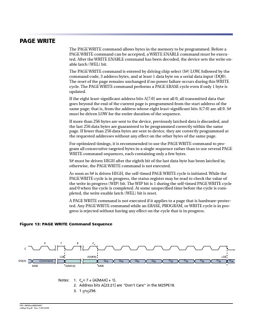
PAGE WRITEThe PAGE WRITE command allows bytes in the memory to be programmed. Before aPAGE WRITE command can be accepted, a WRITE ENABLE command must be execu-ted. After the WRITE ENABLE command has been decoded, the device sets the write en-able latch (WEL) bit.The PAGE WRITE command is entered by driving chip select (S#) LOW, followed by thecommand code, 3 address bytes, and at least 1 data byte on a serial data input (DQ0).The reset of the page remains unchanged if no power failure occurs during this WRITEcycle. The PAGE WRITE command performs a PAGE ERASE cycle even if only 1 byte isupdated.If the eight least-significant address bits A[7:0] are not all 0, all transmitted data thatgoes beyond the end of the current page is programmed from the start address of thesame page; that is, from the address whose eight least-significant bits A[7:0] are all 0. S#must be driven LOW for the entire duration of the sequence.If more than 256 bytes are sent to the device, previously latched data is discarded, andthe last 256 data bytes are guaranteed to be programmed correctly within the samepage. If fewer than 256 data bytes are sent to device, they are correctly programmed atthe requested addresses without any effect on the other bytes of the same page.For optimized timings, it is recommended to use the PAGE WRITE command to pro-gram all consecutive targeted bytes in a single sequence rather than to use several PAGEWRITE command sequences, each containing only a few bytes.S# must be driven HIGH after the eighth bit of the last data byte has been latched in;otherwise, the PAGE WRITE command is not executed.As soon as S# is driven HIGH, the self-timed PAGE WRITE cycle is initiated. While thePAGE WRITE cycle is in progress, the status register may be read to check the value ofthe write in progress (WIP) bit. The WIP bit is 1 during the self-timed PAGE WRITE cycleand 0 when the cycle is completed. At some unspecified time before the cycle is com-pleted, the write enable latch (WEL) bit is reset.A PAGE WRITE command is not executed if it applies to a page that is hardware-protec-ted. Any PAGE WRITE command while an ERASE, PROGRAM, or WRITE cycle is in pro-gress is rejected without having any effect on the cycle that is in progress.Figure 13: PAGE WRITE Command SequenceCDQ[0]Notes: 1.C x= 7 + (A[MAX] + 1).2.Address bits A[23:21] are "Don't Care" in the M25PE16.3. 1 <n<256.PAGE PROGRAMThe PAGE PROGRAM command allows bytes in the memory to be programmed, whichmeans the bits are changed from 1 to 0. Before a PAGE PROGRAM command can be ac-cepted, a WRITE ENABLE command must be executed. After the WRITE ENABLE com-mand has been decoded, the device sets the write enable latch (WEL) bit.The PAGE PROGRAM command is entered by driving chip select (S#) LOW, followed bythe command code, 3 address bytes, and at least 1 data byte on a serial data input(DQ0).If the eight least-significant address bits A[7:0] are not all 0, all transmitted data thatgoes beyond the end of the current page is programmed from the start address of thesame page, that is, from the address whose eight least-significant bits A[7:0] are all 0. S#must be driven LOW for the entire duration of the sequence.If more than 256 bytes are sent to the device, previously latched data is discarded, andthe last 256 data bytes are guaranteed to be programmed correctly within the samepage. If fewer than 256 data bytes are sent to device, they are correctly programmed atthe requested addresses without any effect on the other bytes of the same page.For optimized timings, it is recommended to use the PAGE PROGRAM command toprogram all consecutive targeted bytes in a single sequence rather than to use severalPAGE PROGRAM sequences, each containing only a few bytes.S# must be driven HIGH after the eighth bit of the last data byte has been latched in;otherwise, the PAGE PROGRAM command is not executed.As soon as S# is driven HIGH, the self-timed PAGE PROGRAM cycle is initiated; the cy-cles's duration is t PP. While the PAGE PROGRAM cycle is in progress, the status registermay be read to check the value of the write in progress (WIP) bit. The WIP bit is 1 duringthe self-timed PAGE PROGRAM cycle and 0 when the cycle is completed. At some un-specified time before the cycle is completed, the write enable latch (WEL) bit is reset.A PAGE PROGRAM command is not executed if it applies to a page protected by all theblock-protect bits.Figure 14: PAGE PROGRAM Command SequenceCDQ[0]Notes: 1.Cx = 7 + (A[MAX] + 1).2.Address bits A[23:21] are "Don't Care" in the M25PE16.PAGE ERASEThe PAGE ERASE command sets to 1 (FFh) all bits inside the designated page. Beforethe PAGE ERASE command can be accepted, a WRITE ENABLE command must havebeen executed previously. After the WRITE ENABLE command has been decoded, thedevice sets the write enable latch (WEL) bit.The PAGE ERASE command is entered by driving chip select (S#) LOW, followed by thecommand code and 3 address bytes on a serial data input (DQ0). Any address inside thesector is a valid address for the PAGE ERASE command. S# must be driven LOW for theentire duration of the sequence.S# must be driven HIGH after the eighth bit of the last address byte has been latched in;otherwise, the PAGE ERASE command is not executed. As soon as S# is driven HIGH,the self-timed PAGE ERASE cycle is initiated; the cycle's duration is t PE. While the PAGEERASE cycle is in progress, the status register may be read to check the value of the writein progress (WIP) bit. The WIP bit is 1 during the self-timed PAGE ERASE cycle and 0when the cycle is completed. At some unspecified time before the cycle is completed,the WEL bit is reset.A PAGE ERASE command is not executed if it applies to a page that is protected by theblock-protect bits BP1 and BP0.A PAGE ERASE command issued while an ERASE, PROGRAM, or WRITE cycle is in pro-gress is rejected without having any effect on the cycle that is in progress.Figure 15: SECTOR ERASE Command SequenceCDQ0Notes: 1.C x= 7 + (A[MAX] + 1).2.Address bits A[23:21] are "Don't Care" in the M25PE16.SECTOR ERASEThe SECTOR ERASE command sets all bits inside the chosen sector to 1 (FFh). Beforethe SECTOR ERASE command can be accepted, a WRITE ENABLE command must havebeen executed previously. After the WRITE ENABLE command has been decoded, thedevice sets the write enable latch (WEL) bit.The SECTOR ERASE command is entered by driving chip select (S#) LOW, followed bythe command code and 3 address bytes on a serial data input (DQ0). Any address insidethe sector is a valid address for the SECTOR ERASE command. S# must be driven LOWfor the entire duration of the sequence.S# must be driven HIGH after the eighth bit of the last address byte has been latched in;otherwise, the SECTOR ERASE command is not executed. As soon as S# is driven HIGH,the self-timed SECTOR ERASE cycle is initiated; the cycle's duration is t SE. While theSECTOR ERASE cycle is in progress, the status register may be read to check the value ofthe write in progress (WIP) bit. The WIP bit is 1 during the self-timed SECTOR ERASEcycle and 0 when the cycle is completed. At some unspecified time before the cycle iscompleted, the WEL bit is reset.A SECTOR ERASE command applied to a sector that contains a page that is hardwareprotected is not executed.Any SECTOR ERASE command issued while an ERASE, PROGRAM, or WRITE cycle is inprogress is rejected without having any effects on the cycle that is in progress.Figure 16: SECTOR ERASE Command SequenceCDQ0Notes: 1.C x= 7 + (A[MAX] + 1).2.Address bits A[23:21] are "Don't Care" in the M25PE16.。
ANTHWR5300060中文资料
3/31/02 3/31/02 3/31/02 7/1/01 3/31/02 3/31/02 12/15/02 6/30/02 3/31/02 3/31/02 3/31/02 3/31/02 3/31/02 3/31/02 3/31/02 3/31/02 3/31/02 3/31/02 3/31/02 3/31/02 3/31/02 3/31/02 3/31/02 3/31/02 12/15/02 11/30/01 6/30/02 7/1/01 7/7/02 12/31/02 12/15/02 7/18/03 7/18/03 7/18/03 7/18/03 11/30/01 11/30/01 11/30/01 3/31/02 3/31/02 11/30/01 11/30/01 11/30/01 3/31/02
NEBS and non-NEBS Standard chassis's NEBS and non-NEBS Standard chassis's NEBS and non-NEBS Standard chassis's Antares 3000/50 NEBS and non-NEBS Standard chassis's NEBS and non-NEBS Standard chassis's Obsolete, no replacement AC/101 NEBS and non-NEBS Standard chassis's NEBS and non-NEBS Standard chassis's NEBS and non-NEBS Standard chassis's NEBS and non-NEBS Standard chassis's NEBS and non-NEBS Standard chassis's NEBS and non-NEBS Standard chassis's NEBS and non-NEBS Standard chassis's NEBS and non-NEBS Standard chassis's NEBS and non-NEBS Standard chassis's NEBS and non-NEBS Standard chassis's NEBS and non-NEBS Standard chassis's NEBS and non-NEBS Standard chassis's NEBS and non-NEBS Standard chassis's NEBS and non-NEBS Standard chassis's NEBS and non-NEBS Standard chassis's NEBS and non-NEBS Standard chassis's Obsolete, no replacement CT-Bus Obsolete, no replacement Antares 3000/50 CSP-based speech technologies CSPbased speech technologies CSPbased speech technologies Intel Converged Communications Enterprise Adjunct Media Servers Intel Converged Communications Enterprise Adjunct Media Servers Intel Converged Communications Enterprise Adjunct Media Servers Adjunct Media Servers Obsolete, no replacement Obsolete, no replacement ATM155/PCI H.100 ATM155/PCI H.100 ATM/155 H 100 PCI UTP ATM/155 H 100 PCI UTP ATM155/PCI H.100 ATM155/PCI H.100 ATM25/PCI H.100
MW6S010中文资料
RF Power Field Effect TransistorN-Channel Enhancement-Mode Lateral MOSFETsDesigned for Class A or Class AB base station applications with frequenciesup to 1500 MHz. Suitable for analog and digital modulation and multicarrieramplifier applications.•Typical Two-Tone Performance @ 960 MHz, V DD = 28 Volts, I DQ =125 mA, P out = 10 Watts PEPPower Gain — 18 dBDrain Efficiency — 32%IMD — -37 dBc•Capable of Handling 10:1 VSWR, @ 28 Vdc, 960 MHz, 10 Watts CWOutput Power•Characterized with Series Equivalent Large-Signal Impedance Parameters•On-Chip RF Feedback for Broadband Stability•Qualified Up to a Maximum of 32 V DD Operation•Integrated ESD Protection•N Suffix Indicates Lead-Free Terminations•200°C Capable Plastic Package•In Tape and Reel. R1 Suffix = 500 Units per 24 mm, 13 inch Reel.Table 1. Maximum RatingsRating Symbol Value Unit Drain-Source Voltage V DSS-0.5, +68Vdc Gate-Source Voltage V GS-0.5, +12Vdc Total Device Dissipation @ T C = 25°CDerate above 25°CP D61.40.35WW/°C Storage Temperature Range T stg-65 to +175°C Operating Junction Temperature T J200°C Table 2. Thermal CharacteristicsCharacteristic Symbol Value (1.2)Unit Thermal Resistance, Junction to CaseCase Temperature 80°C, 10 W PEPRθJC2.85°C/W1.MTTF calculator available at /rf. Select Tools/Software/Application Software/Calculators to accessthe MTTF calculators by product.2.Refer to AN1955, Thermal Measurement Methodology of RF Power Amplifiers. Go to /rf.Select Documentation/Application Notes - AN1955.Document Number: MW6S010Rev. 1, 5/2005 Freescale SemiconductorTechnical Data2RF Device DataFreescale SemiconductorMW6S010NR1 MW6S010GNR1 MW6S010MR1 MW6S010GMR1Table 3. ESD Protection CharacteristicsTest MethodologyClass Human Body Model (per JESD22-A114)1A Machine Model (per EIA/JESD22-A115)A Charge Device Model (per JESD22-C101)IIITable 4. Moisture Sensitivity LevelTest MethodologyRating Package Peak TemperatureUnit Per JESD 22-A113, IPC/JEDEC J-STD-0201260°CTable 5. Electrical Characteristics (T C = 25°C unless otherwise noted)CharacteristicSymbolMinTypMaxUnitOff CharacteristicsZero Gate Voltage Drain Leakage Current (V DS = 68 Vdc, V GS = 0 Vdc)I DSS ——10µAdc Zero Gate Voltage Drain Leakage Current (V DS = 28 Vdc, V GS = 0 Vdc)I DSS ——1µAdc Gate-Source Leakage Current (V GS = 5 Vdc, V DS = 0 Vdc)I GSS——1µAdcOn CharacteristicsGate Threshold Voltage(V DS = 10 Vdc, I D = 100 µAdc)V GS(th) 1.5 2.33Vdc Gate Quiescent Voltage(V DS = 28 Vdc, I D = 125 mAdc)V GS(Q)— 3.1—Vdc Drain-Source On-Voltage(V GS = 10 Vdc, I D = 0.3 Adc)V DS(on)—0.270.35VdcDynamic CharacteristicsInput Capacitance(V DS = 28 Vdc ± 30 mV(rms)ac @ 1 MHz, V GS = 0 Vdc)C iss —23—pF Output Capacitance(V DS = 28 Vdc ± 30 mV(rms)ac @ 1 MHz, V GS = 0 Vdc)C oss —10—pF Reverse Transfer Capacitance(V DS = 28 Vdc ± 30 mV(rms)ac @ 1 MHz, V GS = 0 Vdc)C rss—0.32—pFFunctional Tests (In Freescale Test Fixture, 50 ohm system) V DD = 28 Vdc, I DQ = 125 mA, P out = 10 W PEP , f = 960 MHz, Two-Tone Test, 100 kHz Tone Spacing Power Gain G ps 17.51820.5dB Drain EfficiencyηD 3132—%Intermodulation Distortion IMD —-37-33dBc Input Return LossIRL—-18-10dBTypical Performances (In Freescale 450 MHz Demo Board, 50 οhm system) V DD = 28 Vdc, I DQ = 150 mA, P out = 10 W PEP , 420 MHz<Frequency<470 MHz, Two-Tone Test, 100 kHz Tone Spacing Power Gain G ps —20—dB Drain EfficiencyηD —33—%Intermodulation Distortion IMD —-40—dBc Input Return LossIRL—-10—dBMW6S010NR1 MW6S010GNR1 MW6S010MR1 MW6S010GMR13RF Device DataFreescale SemiconductorFigure 1. MW6S010NR1(GNR1/MR1/GMR1) Test Circuit Schematic — 900 MHzZ50.313″ x 0.902″ Microstrip Z60.073″ x 1.080″ Microstrip Z70.073″ x 0.314″ MicrostripPCBRogers ULTRALAM 2000, 0.031″, εr = 2.55Z10.073″ x 0.223″ Microstrip Z20.112″ x 0.070″ Microstrip Z30.213″ x 0.500″ Microstrip Z40.313″ x 1.503″ Microstrip Table 6. MW6S010NR1(GNR1/MR1/GMR1) Test Circuit Component Designations and Values — 900 MHzPartDescriptionPart Number Manufacturer B1Ferrite Bead2743019447Fair-Rite C1, C6, C11, C2047 pF Chip Capacitors100B470JP500X ATC C2, C18, C1922 µF, 35 V Tantalum CapacitorsT491D226K035AS Kemet C3, C16220 µF, 63 V Electrolytic Capacitors, Radial 13668221Phillips C4, C150.1 µF Chip CapacitorsCDR33BX104AKWS Kemet C5, C8, C170.8-8.0 pF Variable Capacitors, Gigatrim 272915L Johanson C7, C1224 pF Chip Capacitors 100B240JP500X ATC C9, C10, C13 6.8 pF Chip Capacitors 100B6R8JP500X ATC C147.5 pF Chip Capacitor 100B7R5JP500X ATC L112.5 nH Inductor A04T-5Coilcraft R11 k Ω Chip ResistorCRCW12061001F100Vishay -Dale4RF Device DataFreescale SemiconductorMW6S010NR1 MW6S010GNR1 MW6S010MR1 MW6S010GMR1Figure 2. MW6S010NR1(GNR1/MR1/GMR1) Test Circuit Component Layout — 900 MHzMW6S010NR1 MW6S010GNR1 MW6S010MR1 MW6S010GMR15RF Device DataFreescale SemiconductorTYPICAL CHARACTERISTICS — 900 MHzP out , OUTPUT POWER (WATTS) AVG.1520119171610100Figure 4. Two-Tone Power Gain versusOutput Power1000.1110P out , OUTPUT POWER (WATTS) AVG.Figure 5. Intermodulation Distortion Productsversus Output PowerG p s , P O W E R G A I N (d B )10−55−150.1TWO−TONE SPACING (MHz)−20−25−30−35−401100Figure 6. Intermodulation Distortion Productsversus Tone Spacing 2948P in , INPUT POWER (dBm)46444240382123252719Figure 7. Pulse CW Output Power versusInput PowerI M D , I N T E R M O D U L A T I O N D I S T O R T I O N (d B c )P o u t , O U T P U T P O W E R (d B m )18−50−450.16RF Device DataFreescale SemiconductorMW6S010NR1 MW6S010GNR1 MW6S010MR1 MW6S010GMR1TYPICAL CHARACTERISTICS — 900 MHzA C P R (dB c )0−60P out , OUTPUT POWER (WATTS) AVG.50−1040−2030−3020−4010−500.1110Figure 8. Single-Carrier CDMA ACPR, PowerGain and Power Added Efficiencyversus Output PowerP out , OUTPUT POWER (WATTS) CWFigure 10. Power Gain versus Output Power 14151912171618468G p s , P O W E R G A I N (d B )500−255f, FREQUENCY (MHz)Figure 11. Broadband Frequency Response−5−10−15−20120011001000900800700600S 11 (d B )16102ηD , D R A I N E F F I C I E N C Y (%), G p s , P O W E R G A I N (d B )MW6S010NR1 MW6S010GNR1 MW6S010MR1 MW6S010GMR17RF Device DataFreescale SemiconductorTYPICAL CHARACTERISTICS21010890T J , JUNCTION TEMPERATURE (°C)Figure 12. MTTF Factor versus Junction TemperatureThis above graph displays calculated MTTF in hours x ampere 2drain current. Life tests at elevated temperatures have correlated to better than ±10% of the theoretical prediction for metal failure. Divide MTTF factor by I D 2 for MTTF in a particular application.107106105120140160180190M T T F F A C T O R (H O U R S x A M P S 2)1002001701501301108RF Device DataFreescale SemiconductorMW6S010NR1 MW6S010GNR1 MW6S010MR1 MW6S010GMR1f MHz Z sourceΩZ load Ω800820840 3.1 + j1.92.7 + j2.22.8 + j1.710.1 + j2.38.3 + j2.58.2 + j3.3V DD = 28 Vdc, I DQ = 125 mA, P out = 10 W PEP 860880900 3.1 + j3.42.9 + j3.73.3 + j3.89.8 + j4.810.6 + j5.69.5 + j5.5920940960 2.8 + j4.43.2 + j4.93.0 + j4.710.1 + j5.911.0 + j6.411.8 + j6.69803.6 + j5.212.1 + j7.1Figure 13. Series Equivalent Source and Load Impedance — 900 MHzZ source =Test circuit impedance as measured fromgate to ground.Z load=Test circuit impedance as measured from drain to ground.ZsourceZloadOutput Matching Networkf = 800 MHzf = 980 MHzZ o = 25 Ωf = 800 MHzf = 980 MHzZ loadZ sourceMW6S010NR1 MW6S010GNR1 MW6S010MR1 MW6S010GMR19RF Device DataFreescale SemiconductorFigure 14. MW6S010NR1(GNR1/MR1/GMR1) Test Circuit Schematic — 450 MHzZ50.475″ x 0.330″ Microstrip Z60.475″ x 0.325″ Microstrip Z8 1.250″ x 0.080″ MicrostripPCBRogers ULTRALAM 2000, 0.030″, εr = 2.55Z10.540″ x 0.080″ Microstrip Z20.365″ x 0.080″ Microstrip Z30.225″ x 0.080″ Microstrip Z4, Z70.440″ x 0.080″ Microstrip R3R4Table 7. MW6S010NR1(GNR1/MR1/GMR1) Test Circuit Component Designations and Values — 450 MHzPartDescriptionPart Number Manufacturer B1, B2Ferrite Bead2743019447Fair-Rite C1 1 µF, 35 V Tantalum Capacitor T491C105K050AS Kemet C2, C1522 µF, 35 V Tantalum Capacitors T491X226K035AS Kemet C3, C140.1 µF Chip Capacitors C1210C104K5RACTR Kemet C4, C9, C10, C13330 pF Chip Capacitors 700A331JP150X ATC C5 4.3 pF Chip Capacitor 100B4R3JP500X ATC C6, C110.6-8.0 pF Variable Capacitors 27291SL Johanson C7, C8, C12 4.7 pF Chip Capacitors 100B4R7JP500X ATC L139 µH Chip Inductor ISC-1210Vishay -Dale R110 Ω Chip Resistor (0805)CRCW080510R0F100Vishay -Dale R2 1 k Ω Chip Resistor (0805)CRCW08051001F100Vishay -Dale R3 1.2 k Ω Chip Resistor (0805)CRCW08051201F100Vishay -Dale R4 2.2 k Ω Chip Resistor (0805)CRCW08052201F100Vishay -Dale R5 5 k Ω Potentiometer 1224WBourns R6 1 k Ω Chip Resistor (1206)CRCW12061001F100Vishay -Dale T1 5 Volt Regulator, Micro 8LP2951On Semiconductor T2NPN TransistorBC847ALT1On Semiconductor10RF Device DataFreescale SemiconductorMW6S010NR1 MW6S010GNR1 MW6S010MR1 MW6S010GMR1Figure 15. MW6S010NR1(GNR1/MR1/GMR1) Test Circuit Component Layout — 450 MHzMW6S010NR1 MW6S010GNR1 MW6S010MR1 MW6S010GMR111RF Device DataFreescale SemiconductorTYPICAL CHARACTERISTICS — 450 MHzI R L , I N P U T R E T U R N L O S S (d B )A C P R (dB c ), A L T 1 (d B c )500400f, FREQUENCY (MHz)Figure 16. 2-Carrier W-CDMA Broadband Performance @ P out = 3 Watts Avg.−21−6−9−12−1518.420.4−6537343128−40−45−50−55ηD , D R AI N E F F I C I E N C Y (%)G p s , P O W E R G A IN (d B )25−60−1820.22019.819.619.419.21918.818.6410420430440450460470480490f, FREQUENCY (MHz)Figure 17. 2-Carrier W-CDMA Broadband Performance @ P out = 7.5 Watts Avg.−50I R L , I N P U T R E T U R N L O S S (d B )A C P R (d B c ), A L T 1 (d B c )500400−14−4−6−8−1016.519−5555504540−30−35−40−45ηD , D R A I N E F F I C I E N C Y (%)G p s , P O W E R G A I N (d B )35−1218.818.518.31817.817.517.31716.8410420430440450460470480490f, FREQUENCY (MHz)Figure 18. Broadband Frequency Response65050530−250−5−15−20S 11S 21−1025201510100150200250300350400450500550600Figure 19. Single-Carrier N-CDMA ACPR, ALT1and ALT2 versus Output Power−80P out , OUTPUT POWER (WATTS) AVG.−10−20−30−40−700.1110−50A L T 1 & A L T 2, C H A N N E L P O W E R (d B c )A C P R , A D J A C E N T C H A N N E L P O W E R R A T I O (dB c )−6012RF Device DataFreescale SemiconductorMW6S010NR1 MW6S010GNR1 MW6S010MR1 MW6S010GMR1f MHz Z sourceΩZ load Ω4004204409.0 + j3.89.6 + j6.68.8 + j5.415.0 + j1.414.3 + j3.315.0 + j4.7V DD = 28 Vdc, I DQ = 150 mA, P out= 10 W PEP 46048050010.6 + j9.511.5 + j13.910.7 + j12.616.3 + j7.316.4 + j11.116.9 + j12.7Figure 20. Series Equivalent Source and Load Impedance — 450 MHzZ source =Test circuit impedance as measured fromgate to ground.Z load=Test circuit impedance as measured from drain to ground.ZsourceZloadOutput Matching Networkf = 400 MHzZ o = 25 ΩZ loadZ sourcef = 500 MHzf = 400 MHzf = 500 MHzMW6S010NR1 MW6S010GNR1 MW6S010MR1 MW6S010GMR113RF Device DataFreescale SemiconductorNOTES14RF Device DataFreescale SemiconductorMW6S010NR1 MW6S010GNR1 MW6S010MR1 MW6S010GMR1PACKAGE DIMENSIONSTO-270-2PLASTICCASE 1265-08ISSUE GMW6S010NR1(MR1)MW6S010NR1 MW6S010GNR1 MW6S010MR1 MW6S010GMR115RF Device DataFreescale SemiconductorTO-270-2 GULLPLASTICCASE 1265A-02ISSUE A BOTTOM VIEWPIN 1.DRAIN 2.GATE 3.SOURCEMW6S010GNR1(GMR1)Information in this document is provided solely to enable system and softwareimplementers to use Freescale Semiconductor products. There are no express orimplied copyright licenses granted hereunder to design or fabricate any integratedcircuits or integrated circuits based on the information in this document.Freescale Semiconductor reserves the right to make changes without further notice toany products herein. Freescale Semiconductor makes no warranty, representation orguarantee regarding the suitability of its products for any particular purpose, nor doesFreescale Semiconductor assume any liability arising out of the application or use ofany product or circuit, and specifically disclaims any and all liability, including withoutlimitation consequential or incidental damages. “Typical” parameters that may beprovided in Freescale Semiconductor data sheets and/or specifications can and dovary in different applications and actual performance may vary over time. All operatingparameters, including “Typicals”, must be validated for each customer application bycustomer’s technical experts. Freescale Semiconductor does not convey any licenseunder its patent rights nor the rights of others. Freescale Semiconductor products arenot designed, intended, or authorized for use as components in systems intended forsurgical implant into the body, or other applications intended to support or sustain life,or for any other application in which the failure of the Freescale Semiconductor productcould create a situation where personal injury or death may occur. Should Buyerpurchase or use Freescale Semiconductor products for any such unintended orunauthorized application, Buyer shall indemnify and hold Freescale Semiconductorand its officers, employees, subsidiaries, affiliates, and distributors harmless against allclaims, costs, damages, and expenses, and reasonable attorney fees arising out of,directly or indirectly, any claim of personal injury or death associated with suchunintended or unauthorized use, even if such claim alleges that FreescaleSemiconductor was negligent regarding the design or manufacture of the part.Freescale t and the Freescale logo are trademarks of Freescale Semiconductor, Inc.All other product or service names are the property of their respective owners.Freescale Semiconductor, Inc. 2005. All rights reserved.How to Reach Us:Home Page:E-mail:support@USA/Europe or Locations Not Listed:Freescale SemiconductorTechnical Information Center, CH3701300 N. Alma School RoadChandler, Arizona 85224+1-800-521-6274 or +1-480-768-2130support@Europe, Middle East, and Africa:Freescale Halbleiter Deutschland GmbHTechnical Information CenterSchatzbogen 781829 Muenchen, Germany+44 1296 380 456 (English)+46 8 52200080 (English)+49 89 92103 559 (German)+33 1 69 35 48 48 (French)support@Japan:Freescale Semiconductor Japan Ltd.HeadquartersARCO Tower 15F1-8-1, Shimo-Meguro, Meguro-ku,Tokyo 153-0064Japan0120 191014 or +81 3 5437 9125support.japan@Asia/Pacific:Freescale Semiconductor Hong Kong Ltd.Technical Information Center2 Dai King StreetTai Po Industrial EstateTai Po, N.T., Hong Kong+800 2666 8080@For Literature Requests Only:Freescale Semiconductor Literature Distribution CenterP.O. Box 5405Denver, Colorado 802171-800-441-2447 or 303-675-2140Fax: 303-675-2150LDCForFreescaleSemiconductor@。
SA06中文资料

Model No. Max output wattage (W) Input Input filter Voltage (V.DC.) Voltage accuracy Current (mA) max Line regulation (HL-LL) (typ.) Output Load regulation (10-100%) (typ.) Ripple Noise Efficiency Switching frequency Over current protection Protection Over voltage protection Short circuit protection Voltage Isolation Resistance Capacitance Operating temperature Storage temperature Case temperature Environment Temperature coefficient Humidity MTBF Dimension (L x W x H) Case Material Physical Weight Cooling method
ELECTRICAL SPECIFICATIONS
Model No. Max. output wattage (W) Input voltage (V.DC.) Output voltage (V.DC.) SA 06-24-3.3S 5W 24V (18-36V) 3.3V / 1500mA SA 06-24-5S 6W 24V (18-36V) 5V / 1200mA SA 06-24-12S 6W 24V (18-36V) 12V / 500mA SA 06-24-15S 6W 24V (18-36V) 15V / 400mA SA 06-24-24S 6W 24V (18-36V) 24V / 250mA
EQW006A0B1Z;EQW006A0B1;中文规格书,Datasheet资料

Electrical Specifications
Unless otherwise indicated, specifications apply over all operating input voltage, resistive load, and temperature conditions.
Absolute Maximum Ratings
Stresses in excess of the absolute maximum ratings can cause permanent damage to the device. These are absolute stress ratings only, functional operation of the device is not implied at these or any other conditions in excess of those given in the operations sections of the data sheet. Exposure to absolute maximum ratings for extended periods can adversely affect the device reliability.
Hale Waihona Puke
Low output ripple and noise Surface mount or through hole Cost efficient open frame design Remote On/Off positive logic (primary referenced) Remote Sense Adjustable output voltage Constant switching frequency (330 kHz) Output over voltage and over current protection Over temperature protection Input undervoltage lockout Wide operating temperature range (-40°C to 85°C) UL* 60950 Recognized, CSA C22.2 No. 60950-00 ‡ rd Certified, and VDE 0805 (IEC60950, 3 edition) Licensed CE mark meets 73/23/EEC and 93/68/EEC directives ISO** 9001 and ISO14001 certified manufacturing facilities Meets the voltage and current requirements for ETSI 300-132-2 and complies with and licensed for Basic rd insulation rating per IEC60950 3 edition
W5100数据手册
W5100 数据手册
Version 1.2.4
数 据 手 册
© 2010 WIZnet Co., Inc. 更多信息,请登录我们的官方网站 http://www.wiznet.co.kr
© Copyright 2009-2010 WIZnet Co., Inc. All rights reserv Copyright 2009-2010 WIZnet Co., Inc. All rights reserved.
W5100 简介
W5100 是一款多功能的单片网络接口芯片,内部集成有 10/100 以太网控制器,主要 应用于高集成、高稳定、高性能和低成本的嵌入式系统中。使用 W5100 可以实现没有操作 系统的 Internet 连接。W5100 与 IEEE802.3 10BASE-T 和 802.3u 100BASE-TX 兼容。 W5100 内部集成了全硬件的、且经过多年市场验证的 TCP/IP 协议栈、以太网介质传 输层(MAC)和物理层(PHY) 。硬件 TCP/IP 协议栈支持 TCP,UDP,IPv4,ICMP,ARP, IGMP 和 PPPoE, 这些协议已经在很多领域经过了多年的验证。 W5100 内部还集成有 16KB 存储器用于数据传输。 使用 W5100 不需要考虑以太网的控制, 只需要进行简单的端口编程。 W5100 提供 3 种接口:直接并行总线、间接并行总线和 SPI 总线。W5100 与 MCU 接 口非常简单,就像访问外部存储器一样。
W5100
数 据 手 册
应用产品
W5100 可用于多种嵌入式应用产品,包括: - 家用网络设备:机顶盒,PVRs,数字媒体适配器 - 串口转以太网:访问控制,LED 显示器,无线 AP 等 - 并行转以太网:POS/Mini 打印机,复印机 - USB 转以太网:存储设备,网络打印机 - GPIO 转以太网:家用网络传感器 - 安防系统:DVRs,网络照相机,终端机 - 工业和楼宇自动化 - 医用检测设备 - 嵌入式服务器
W5300中文用户数据手册-v1

W5300中文用户数据手册v1一、产品概述1. 高性能处理器,保证流畅运行。
2. 大容量存储空间,满足您的存储需求。
3. 丰富接口,方便连接各种设备。
4. 定制化系统,轻松应对各种应用场景。
二、包装清单1. W5300主机2. 电源适配器3. USB数据线4. 用户数据手册(即本手册)5. 保修卡如有缺失,请及时与销售商联系。
三、设备外观与按键功能1. 电源键:长按开启/关闭设备,短按进入休眠状态。
2. 音量键:调节设备音量。
3. Home键:返回主界面。
4. 功能键:自定义按键,可设置快捷功能。
5. USB接口:连接USB设备,如U盘、键盘等。
6. 耳机接口:连接耳机。
7. 充电接口:连接电源适配器进行充电。
四、初始设置4.1 开启设备1. 将电源适配器插入电源插座。
2. 将充电线一端插入设备充电接口,另一端连接电源适配器。
3. 长按电源键,开启设备。
4.2 语言选择1. 在开机过程中,根据提示选择中文简体或中文繁体。
2. 按照屏幕提示完成剩余设置。
4.3 连接WiFi1. 在主界面找到“设置”应用。
2. 选择“无线和网络”选项,进入WiFi设置。
3. 按照屏幕提示连接到您的WiFi网络。
五、基本操作5.1 滑动屏幕1. 向上滑动:查看通知栏。
2. 向下滑动:快速设置。
3. 向左滑动:切换上一个应用。
4. 向右滑动:切换下一个应用。
5.2 点按屏幕1. 单击:选中某个应用或选项。
2. 长按:弹出快捷菜单或进入编辑状态。
5.3 使用应用1. 在主界面,找到您想要使用的应用图标。
2. 图标,进入应用。
3. 根据应用提示进行操作。
请继续阅读下一部分,了解更多关于W5300的高级功能和使用技巧。
六、系统设置与个性化6.1 调整屏幕亮度和分辨率为了让您的视觉体验更加舒适,您可以自定义屏幕亮度和分辨率:1. 在主界面找到“设置”应用。
2. 选择“显示”选项。
3. 在“亮度”中,拖动滑块调整亮度,或开启自动调节亮度。
RM05-60RGB中文资料

Power SuppliesRM-GB SeriesAC InputSingle Output, Long LifeFEATURES•Remote ON-OFF .•Remote sensing.•Parallel connection is possible.•These low noise power supplies are CISPR standard compliant. PART NUMBERS AND RATINGSOutput voltage(V)30W type 50W type75W type Current(A)Part No.Current(A)Part No.Current(A)Part No.56RM05-6R0GB 10RM05-10RGB 15RM05-15RGB 9 3.3RM09-3R3GB 6RM09-6R0GB 8RM09-8R0GB 12 2.5RM12-2R5GB 5RM12-5R0GB 6.3RM12-6R3GB 152RM15-2R0GB 4RM15-4R0GB 5RM15-5R0GB 24 1.3RM24-1R3GB2.5RM24-2R5GB3.2RM24-3R2GB 481.3RM48-1R3GB1.6RM48-1R6GBOutput voltage(V)100W type 150W type 300W type Current(A)Part No.Current(A)Part No.Current(A)Part No.520RM05-20RGB 30RM05-30RGB 60RM05-60RGB 911RM09-11RGB 16RM09-16RGB 32RM09-32RGB 128.5RM12-8R5GB 12RM12-12RGB 27RM12-27RGB 157RM15-7R0GB 10RM15-10RGB 23RM15-23RGB 24 4.5RM24-4R5GB 6RM24-6R0GB 16RM24-16RGB 482.2RM48-2R2GB 3RM48-3R0GB 6RM48-6R0GBPower SuppliesRM-GB SeriesAC InputSingle Output, Long LifeSPECIFICATIONS 30W TYPE∗ Current rating(maximum output current) is determined for 0 to +50°C. Derating is required when used outside this temperature range.Part No.RM05-6R0GB RM09-3R3GB RM12-2R5GB RM15-2R0GB RM24-1R3GB Output voltage, current ∗ 5V • 6A 9V • 3.3A 12V • 2.5A 15V • 2A 24V • 1.3A Maximum output power W 333333.73334.4Input requirements Input voltage Eac V 85 to 132[Rating:100-115]Input frequency Hz 47 to 440[Rating:50-60](Single phase)Input capacitance VA 80max.[At maximum output power]Fuse rating A 3.15[Internal]Surge current A 15/17max.[25°C, input and output ratings, 1st surge current, reset after roughly 5s min.]Leakage current mA 0.5max.(0.3typ.)[25°C, input and output ratings]Efficiency%75typ.[25°C, input and output ratings]Output characteristics Output voltageV 59121524Voltage variable range V 4.25 to 5.57.2 to 109.5 to 13.512 to 16.519 to 26.5Maximum output current ∗ A 6 3.3 2.521.3Overvoltage threshold V 5.8 to 6.910.5 to 12.513.7 to 15.717 to 1927 to 30.5Overcurrent thresholdA 6.6 to 7.8 3.7 to 4.3 2.8 to 3.3 2.2 to 2.61.5 to 1.8Voltage stability Input variation %0.8max.(0.5typ.)[Within the input voltage range]T otal variation ±2max.(±1.3typ.)Load variation%1max.(0.5typ.)[10 to 100% load]Temperature variation% 1.2max.(0.4typ.)[0 to +50°C]Drift%0.5max.[25°C, input and output ratings, after input voltage ON for 30min to 8h]Dynamic load%/ms ±4max./1max.[50 to 100% sudden load change]Ripple Ep-pmV 50max.50max.80max.80max.100max.Ripple noise Ep-p mV Output voltage × 0.5%+50max.[50MHz max.]Start up time ms 100max.(50typ.)[25°C, input and output ratings]Hold up timems20min.(35typ.)[25°C, input and output ratings]Accessory equipment Overvoltage protection Voltage shielding type, recovers upon reset.Overcurrent protection Fixed current and output voltage threshold type, automatic recovery.Remote ON-OFF Y es(Floating)Remote sensing Y esStandardsSafety standardsUL478, CSA ELECTRICAL BULLETIN No.1402 approved.Noise terminal voltage CISPR standard compliant.ConstructionExternal dimensions H × W × L mm 130 × 35 ×146Weightg650max.Mounting method Can be attached to 4 sides.Case materialAluminum(Phosphoric acid anodized surface)Power SuppliesRM-GB SeriesAC InputSingle Output, Long LifeSPECIFICATIONS 50W TYPE∗ Current rating(maximum output current) is determined for 0 to +50°C. Derating is required when used outside this temperature range.Part No.RM05-10RGB RM09-6R0GB RM12-5R0GB RM15-4R0GB RM24-2R5GB RM48-1R3GB Output voltage, current ∗ 5V • 10A 9V • 6A 12V • 5A 15V • 4A 24V • 2.5A 48V • 1.3A Maximum output power W 556068666669Input requirements Input voltage Eac V 85 to 132[Rating:100-115]Input frequency Hz 47 to 440[Rating:50-60](Single phase)Input capacitance VA 180max.[At maximum output power]Fuse rating A 3.15[Internal]Surge current A 15/17max.[25°C, input and output ratings, 1st surge current, reset after roughly 5s min.]Leakage current mA 0.5max.(0.3typ.)[25°C, input and output ratings]Efficiency%78typ.[25°C, input and output ratings]Output characteristics Output voltageV 5912152448Voltage variable range V 4 to 5.57.2 to 109.5 to 13.512 to 16.519 to 26.538.4 to 53Maximum output current ∗ A 106542.51.3Overvoltage threshold V 6 to 6.510.5 to 1114 to 14.517 to 17.527 to 27.555 to 57Overcurrent thresholdA 11.5 to 12.5 6.9 to 7.5 5.7 to 6.3 4.6 to 52.8 to3.21.5 to 1.7Voltage stability Input variation %0.8max.(0.5typ.)[Within the input voltage range]T otal variation ±2max.(±1.3typ.)Load variation%1max.(0.5typ.)[10 to 100% load]Temperature variation% 1.2max.(0.4typ.)[0 to +50°C]Drift%0.5max.[25°C, input and output ratings, after input voltage ON for 30min to 8h]Dynamic load%/ms ±4max./1max.[50 to 100% sudden load change]Ripple Ep-pmV 50max.50max.80max.80max.100max.100max.Ripple noise Ep-p mV Output voltage × 0.5%+50max.[50MHz max.]Start up time ms 150max.(90typ.)[25°C, input and output ratings]500max.(250typ.)Hold up timems20min.(35typ.)[25°C, input and output ratings]Accessory equipment Overvoltage protection Voltage shielding type, recovers upon reset.Overcurrent protection Fixed current and output voltage threshold type, automatic recovery.Remote ON-OFF Y es(Floating)Remote sensing Y esStandardsSafety standardsUL478, CSA ELECTRICAL BULLETIN No.1402 approved.Noise terminal voltage CISPR standard compliant.ConstructionExternal dimensions H × W × L mm 130 × 55 ×191Weightkg1.1max.Mounting method Can be attached to 4 sides.Case materialAluminum(Phosphoric acid anodized surface)Power SuppliesRM-GB SeriesAC InputSingle Output, Long LifeSPECIFICATIONS 75W TYPE∗ Current rating(maximum output current) is determined for 0 to +50°C. Derating is required when used outside this temperature range.Part No.RM05-15RGB RM09-8R0GB RM12-6R3GB RM15-5R0GB RM24-3R2GB RM48-1R6GB Output voltage, current ∗ 5V • 15A 9V • 8A 12V • 6.3A 15V • 5A 24V • 3.2A 48V • 1.6A Maximum output power W 82.5808582.58585Input requirements Input voltage Eac V 85 to 132[Rating:100-115]Input frequency Hz 47 to 440[Rating:50-60](Single phase)Input capacitance VA 220max.[At maximum output power]Fuse rating A 4[Internal]Surge current A 15/17max.[25°C, input and output ratings, 1st surge current, reset after roughly 5s min.]Leakage current mA 0.5max.(0.3typ.)[25°C, input and output ratings]Efficiency%78typ.[25°C, input and output ratings]Output characteristics Output voltageV 5912152448Voltage variable range V 4 to 5.57.2 to 109.5 to 13.512 to 16.519 to 26.538.4 to 53Maximum output current ∗ A 158 6.353.21.6Overvoltage threshold V 6 to 6.510.5 to 1114 to 14.517 to 17.527 to 27.555 to 57Overcurrent thresholdA 17.2 to 18.89.2 to 107.2 to 7.9 5.7 to 6.33.6 to 41.8 to 2Voltage stability Input variation %0.8max.(0.5typ.)[Within the input voltage range]T otal variation ±2max.(±1.3typ.)Load variation%1max.(0.5typ.)[10 to 100% load]Temperature variation% 1.2max.(0.4typ.)[0 to +50°C]Drift%0.5max.[25°C, input and output ratings, after input voltage ON for 30min to 8h]Dynamic load%/ms ±4max./1max.[50 to 100% sudden load change]Ripple Ep-pmV 50max.50max.80max.80max.100max.100max.Ripple noise Ep-p mV Output voltage × 0.5%+50max.[50MHz max.]Start up time ms 150max.(90typ.)[25°C, input and output ratings] 500max.(250typ.)Hold up timems20min.(35typ.)[25°C, input and output ratings]Accessory equipment Overvoltage protection Voltage shielding type, recovers upon reset.Overcurrent protection Fixed current and output voltage threshold type, automatic recovery.Remote ON-OFF Y es(Floating)Remote sensing Y esStandardsSafety standardsUL478, CSA ELECTRICAL BULLETIN No.1402 approved.Noise terminal voltage CISPR standard compliant.ConstructionExternal dimensions H × W × L mm 130 × 55 ×224Weightkg1.5max.Mounting method Can be attached to 4 sides.Case materialAluminum(Phosphoric acid anodized surface)Power SuppliesRM-GB SeriesAC InputSingle Output, Long LifeSPECIFICATIONS 100W TYPE∗ Current rating(maximum output current) is determined for 0 to +50°C. Derating is required when used outside this temperature range.Part No.RM05-20RGB RM09-11RGB RM12-8R5GB RM15-7R0GB RM24-4R5GB RM48-2R2GB Output voltage, current ∗ 5V • 20A 9V • 11A 12V • 8.5A 15V • 7A 24V • 4.5A 48V • 2.2A Maximum output power W 110110115116119117Input requirements Input voltage Eac V 85 to 132[Rating:100-115]Input frequency Hz 47 to 440[Rating:50-60](Single phase)Input capacitance VA 220max.[At maximum output power]Fuse rating A 5[Internal]Surge current A 15/17max.[25°C, input and output ratings, 1st surge current, reset after roughly 5s min.]Leakage current mA 0.5max.(0.3typ.)[25°C, input and output ratings]Efficiency%78typ.[25°C, input and output ratings]Output characteristics Output voltageV 5912152448Voltage variable range V 4 to 5.57.2 to 109.5 to 13.512 to 16.519 to 26.538.4 to 53Maximum output current ∗ A 20118.574.52.2Overvoltage threshold V 6 to 6.510.5 to 1114 to 14.517 to 17.527 to 27.555 to 57Overcurrent thresholdA 23 to 2512.6 to 13.89.7 to 10.78 to 8.85.1 to 5.72.5 to 2.8Voltage stability Input variation %0.8max.(0.5typ.)[Within the input voltage range] T otal variation ±2max.(±1.3typ.)Load variation%1max.(0.5typ.)[10 to 100% load]Temperature variation% 1.2max.(0.4typ.)[0 to +50°C]Drift%0.5max.[25°C, input and output ratings, after input voltage ON for 30min to 8h]Dynamic load%/ms ±4max./1max.[50 to 100% sudden load change]Ripple Ep-pmV 50max.50max.80max.80max.100max.100max.Ripple noise Ep-p mV Output voltage × 0.5%+50max.[50MHz max.]Start up time ms 150max.(90typ.)[25°C, input and output ratings]500max.(250typ.)Hold up timems20min.(35typ.)[25°C, input and output ratings]Accessory equipment Overvoltage protection Voltage shielding type, recovers upon reset.Overcurrent protection Fixed current and output voltage threshold type, automatic recovery.Remote ON-OFF Y es(Floating)Remote sensing Y esStandardsSafety standardsUL478, CSA ELECTRICAL BULLETIN No.1402 approved.Noise terminal voltage CISPR standard compliant.ConstructionExternal dimensions H × W × L mm 130 × 83 ×224Weightkg1.8max.Mounting method Can be attached to 4 sides.Case materialAluminum(Phosphoric acid anodized surface)Power SuppliesRM-GB SeriesAC InputSingle Output, Long LifeSPECIFICATIONS 150W TYPE∗ Current rating(maximum output current) is determined for 0 to +50°C. Derating is required when used outside this temperature range.Part No.RM05-30RGB RM09-16RGB RM12-12RGB RM15-10RGB RM24-6R0GB RM48-3R0GB Output voltage, current ∗ 5V • 30A 9V • 16A 12V • 12A 15V • 10A 24V • 6A 48V • 3A Maximum output power W 165160162165159159Input requirements Input voltage Eac V 85 to 132[Rating:100-115]Input frequency Hz 47 to 440[Rating:50-60](Single phase)Input capacitance VA 390max.[At maximum output power]Fuse rating A 6[Internal]Surge current A 15/17max.[25°C, input and output ratings, 1st surge current, reset after roughly 5s min.]Leakage current mA 0.5max.(0.3typ.)[25°C, input and output ratings]Efficiency%78typ.[25°C, input and output ratings]Output characteristics Output voltageV 5912152448Voltage variable range V 4 to 5.57.2 to 109.5 to 13.512 to 16.519 to 26.538.4 to 53Maximum output current ∗ A 3016121063Overvoltage threshold V 6 to 6.510.5 to 1114 to 14.517 to 17.527 to 27.555 to 57Overcurrent thresholdA 34.5 to 37.518 to 2013.8 to 1511.5 to 12.56.9 to7.53.4 to 3.8Voltage stability Input variation %0.8max.(0.5typ.)[Within the input voltage range]T otal variation ±2max.(±1.3typ.)Load variation%1max.(0.5typ.)[10 to 100% load]Temperature variation% 1.2max.(0.4typ.)[0 to +50°C]Drift%0.5max.[25°C, input and output ratings, after input voltage ON for 30min to 8h]Dynamic load%/ms ±4max./1max.[50 to 100% sudden load change]Ripple Ep-pmV 50max.50max.80max.80max.100max.100max.Ripple noise Ep-p mV Output voltage × 0.5%+50max.[50MHz max.]Start up time ms 150max.(90typ.)[25°C, input and output ratings]500max.(250typ.)Hold up timems20min.(35typ.)[25°C, input and output ratings]Accessory equipment Overvoltage protection Voltage shielding type, recovers upon reset.Overcurrent protection Fixed current and output voltage threshold type, automatic recovery.Remote ON-OFF Y es(Floating)Remote sensing Y esStandardsSafety standardsUL478, CSA ELECTRICAL BULLETIN No.1402 approved.Noise terminal voltage CISPR standard compliant.ConstructionExternal dimensions H × W × L mm 130 × 103 ×224Weightkg2.3max.Mounting method Can be attached to 4 sides.Case materialAluminum(Phosphoric acid anodized surface)Power SuppliesRM-GB SeriesAC InputSingle Output, Long LifeSPECIFICATIONS 300W TYPE∗ Current rating(maximum output current) is determined for 0 to +50°C. Derating is required when used outside this temperature range.Part No.RM05-60RGB RM09-32RGB RM12-27RGB RM15-23RGB RM24-16RGB RM48-6R0GB Output voltage, current ∗ 5V • 60A 9V • 32A 12V • 27A 15V • 23A 24V • 16A 48V • 6A Maximum output power W 330320365380384318Input requirements Input voltage Eac V 85 to 132[Rating:100-115]Input frequency Hz 47 to 440[Rating:50-60](Single phase)Input capacitance VA 750max.[At maximum output power]Fuse rating A 15[Internal]Surge current A 20/25max.[25°C, input and output ratings, 1st surge current, reset after roughly 40s min.]Leakage current mA 0.5max.(0.3typ.)[25°C, input and output ratings]Efficiency%80typ.[25°C, input and output ratings]Output characteristics Output voltageV 5912152448Voltage variable range V 4 to 5.57.2 to 109.5 to 13.512 to 16.519 to 26.538.4 to 53Maximum output current ∗ A 60322723166Overvoltage threshold V 6 to 6.510.5 to 1114 to 14.517 to 17.527 to 27.555 to 57Overcurrent thresholdA 66 to 7235.5 to 4130 to 3425 to 2917 to 18.56.6 to7.4Voltage stability Input variation %0.8max.(0.5typ.)[Within the input voltage range]T otal variation ±2max.(±1.3typ.)Load variation%1max.(0.5typ.)[10 to 100% load]T emperature variation% 1.2max.(0.4typ.)[0 to +50°C]Drift%0.5max.[25°C, input and output ratings, after input voltage ON for 30min to 8h]Dynamic load%/ms ±4max./1max.[50 to 100% sudden load change]Ripple Ep-pmV 50max.50max.80max.80max.100max.100max.Ripple noise Ep-p mV Output voltage × 0.5%+50max.[50MHz max.]Start up time ms 150max.(90typ.)[25°C, input and output ratings]500max.(250typ.)Hold up timems20min.(30typ.)[25°C, input and output ratings]Accessory equipment Overvoltage protection Voltage shielding type, recovers upon reset(interval approx. 40s).Overcurrent protection Fixed current and output voltage threshold type, automatic recovery.Remote ON-OFF Y es(Floating)Remote sensing Y esStandardsSafety standardsUL478, CSA ELECTRICAL BULLETIN No.1402 approved.Noise terminal voltage CISPR standard compliant.ConstructionExternal dimensions H × W × L mm 130 × 153 ×224Weightkg3.8max.Mounting method Can be attached to 4 sides.Case materialAluminum(Phosphoric acid anodized surface)A112_RM_GB980403Power SuppliesRM-GB SeriesAC InputSingle Output, Long LifeTERMINAL DESIGNATIONS AND FUNCTIONS 30W TYPE 50W AND 75W TYPES100W TYPE150W TYPE300W TYPET erminal No. 1: Output voltage adjustment trim(V . ADJ)Adjusts output voltage.T erminal No. 2: Remote sensing terminals(+S, –S)These are normally jumpered. When controlling voltage to the load, please remove jumper, and wire these.T erminal No. 3: DC output terminals(+, –)Connect to load.T erminal No. 4: Remote ON-OFF terminals(+RC, –RC)Output is turned ON-OFF by disconnecting-connecting the RC terminals(output ON when open). RC terminals are floating.Terminal No. 5: AC input terminals(H, N, AC.100/115V)Connect to AC.100/115V single phase power supply.Terminal No. 6: Frame ground terminal(G)Connect to earth ground. This is connected to the case.Terminal No. 7: Overcurrent adjustment trim(OC)This is adjusted at the factory prior to shipment.Terminal No. 8: Overvoltage adjustment trim(OV)This is adjusted at the factory prior to shipment.Terminal No. 9: Monitor terminals(MONITOR, +, –)This terminal is used to monitor DC current output.Load lines should not be connected to these monitor terminals.These monitor terminals should be jumpered when the remote monitoring feature is not in use.Terminal No. 10: DC output terminals (DC OUTPUT, +, –) 150W typeConnect to load. Maximum permissible current for a single ter-minal is 25A. Use of terminal pairs is recommended.T erminal No. 11: DC output terminals(DC OUTPUT, +, –)300W typeConnect to load. Maximum permissible current for a single ter-minal is 40A. Use of terminal pairs is recommended.。
5KW家用光伏系统说明书共9页

5KW家用光伏系统技术说明书版本号:S1.0石家庄通合电子科技股份有限公司目录一、概述 (1)二、电气参数 (1)三、系统原理框图及工作模式切换概述 (2)四、保护功能 (3)五、操作说明 (4)六、正常使用的环境条件 (8)七、绝缘耐压 (8)八、结构外观效果图 (8)九、外壳防护等级 (9)十、注意事项 (9)十一、运输和存储 (9)一、概述1.1 产品特点5KW家用光伏系统是通合公司专为户用设计的一款后备式一体化接入设备,此家用系统主要有并网发电、储能及后备供电的功能。
市电正常时,系统将光伏组件的直流电能转化为与电网同频率、同相位的正弦波电流,一部分给用户负载供电,剩余电力馈入电网;市电异常时,迅速切换到离网工作模式,由太阳能电池板和蓄电池共同给系统供电,保证用户负载的正常运行。
系统主要由光伏电池板、充电机、储能装置(锂电池)、光伏并网离网一体型逆变器、输出控制单元和监控装置等几部分。
具有以下特点:(1)输入电压范围宽;(2)输出稳频稳压,波形纯净;(3)开机延时软启动,大大减小电源启动时对设备和电网的冲击;(4)工作模式(并网优先或负载优先)可自由设置;(5)完善的保护功能:输入防反接、输入过/欠压保护、输出过/欠压保护、方阵绝缘阻抗监测等;(6)液晶屏显示,提供完备的人机操作界面,显示尽可能丰富的系统状态信息;(7)系统的组件均为自冷型工作方式,无噪声、工作可靠性高;(8)提供WiFi数据链接,支持实时数据通讯功能;二、电气参数三、系统原理框图及工作模式切换概述5.1系统原理框图系统模块图如下所示:5.2工作模式概述系统工作在并网状态时,分为负载优先和并网优先两种工作模式。
5.2.1负载优先储能装置(锂电池)充满电后,市电正常时其始终处于后备状态,不给逆变器提供电能。
在市电异常后,光伏电池板不能够提供满足负载要求的电能,锂电池才开始放电,最大限度的保证负载的供电正常。
5.2.2并网优先:根据预先设置好的储能装置(锂电池)“允许放电时间”(用户可设),太阳能电池板和储能装置(锂电池)通过逆变器共同向电网回馈电能,直至达到储能装置(锂电池)“终止放电时间”或放电终止电压后,储能装置(锂电池)停止放电。
W5100S数据手册V1.0.0

PHYCR1 (PHY 控制寄存器 1) ...................................................... 35 SLCR (SOCKET-less 控制寄存器) ................................................... 36 SLRTR (SOCKET-less 重传超时时间寄存器) ...................................... 37 SLRCR (SOCKET-less 重传次数寄存器) ........................................... 37 SLPIPR (SOCKET-less 目标 IP 地址寄存器) ........................................ 37 SLPHAR (SOCKET-less 目标 MAC 地址寄存器) ................................... 37 PINGSEQR (PING 序列号寄存器) ................................................... 38 PINGIDR (PING ID 寄存器) .......................................................... 38 SLIMR (SOCKET-less 中断屏蔽寄存器) ............................................ 38 SLIR (SOCKET-less 中断寄存器) .................................................... 39 CLKLCKR (时钟锁定寄存器) ......................................................... 39 NETLCKR (网络锁定寄存器)......................................................... 40 PHYLCKR (PHY 锁定寄存器 ) ....................................................... 40 VERR (芯片版本寄存器) ............................................................. 40 TCNTR (Ticker 计数器寄存器) ..................................................... 40 TCNTCLR (Ticker 计数器清除寄存器) ............................................ 40 Sn_MR (SOCKET n 模式寄存器) .................................................... 41 Sn_CR (SOCKET n 控制寄存器) .................................................... 42 Sn_IR (SOCKET n 中断寄存器) ..................................................... 44 Sn_SR (SOCKET n 状态寄存器) ..................................................... 44 Sn_PORTR (SOCKET n 源端口寄存器)............................................. 46 Sn_DHAR (SOCKET n 目标 MAC 地址寄存器) ..................................... 47 Sn_DIPR (SOCKET n 目标 IP 地址寄存器) ......................................... 47 Sn_DPORTR (SOCKET n 目标端口寄存器) ........................................ 48 Sn_MSS (SOCKET n 最大分段寄存器) ............................................. 48 Sn_PROTOR (SOCKET n IP 协议寄存器) .......................................... 48 Sn_TOS (SOCKET n IP 服务类型寄存器) .......................................... 49 Sn_TTL (SOCKET n IP 生存时间寄存器) .......................................... 49 Sn_RXBUF_SIZE (SOCKET n 接收缓存大小寄存器) .............................. 49 Sn_TXBUF_SIZE (SOCKET n 发送缓存大小寄存器) .............................. 49 Sn_TX_FSR (SOCKET n 空闲发送缓存寄存器) ................................... 50 Sn_TX_RD (SOCKET n 发送读指针寄存器) ........................................ 50 Sn_TX_WR (SOCKET n 发送写指针寄存器) ....................................... 50 Sn_RX_RSR (SOCKET n 接收大小寄存器) ......................................... 51 Sn_RX_RD (SOCKET n 接收读指针寄存器) ....................................... 51 Sn_RX_WR (SOCKET n 接收写指针寄存器) ....................................... 51 Sn_IMR (SOCKET n 中断屏蔽寄存器) .............................................. 52 Sn_FRAGR (SOCKET n IP 包头片段偏移寄存器) .................................. 52
W04G;W005G;W01G;W02G;W08G;中文规格书,Datasheet资料

e 3W005G - W10G1.5A GLASS PASSIVATED BRIDGE RECTIFIERFeaturesMaximum Ratings and Electrical Characteristics@ T A = 25°C unless otherwise specifiedMechanical DataSingle phase, 60Hz, resistive or inductive load. For capacitive load, derate current by 20%.Notes: 1. Thermal resistance from junction to case mounted on PC board with 13 x 13mm (0.03mm thick) land areas. 2. Per element, measured at 1.0MHz and applied reverse voltage of 4.0V DC.3. EC Directive 2002/95/EC(RoHS) revision 13.2.2003. Glass and High Temperature Solder Exemptions Applied, see EU Directive AnnexNotes 5 and 7.·Glass Passivated Die Construction·Low Forward Voltage Drop, High Current Capability ·Surge Overload Rating to 50A Peak ·Ideal for Printed Circuit Boards·Case to Terminal Isolation Voltage 1500V ·UL Listed Under Recognized Component Index, File Number E94661·Lead Free Finish, RoHS Compliant (DC 514+) (Note 3)·Case: WOG·Case Material: Molded Plastic. UL Flammability Classification Rating 94V-0·Moisture Sensitivity: Level 1 per J-STD-020C·Terminals: Finish ¾ Silver. Plated Leads Solderable per MIL-STD-202, Method 208·Polarity: As marked on Body ·Marking: Type Number·Weight: 1.3 grams (approximate)0.010.11.0100.20.6 1.0 1.4I , I N S T A N T A N E O U S F O R W A R D C U R R E N T (A )F V , INSTANTANEOUS FORWARD VOLTAGE (V)FFig. 2 Typical Forward Characteristics1020304050110100I , P E A K F O R W A R D S U R G E C U R R E N T (A )F S M NUMBER OF CYCLES AT 60 HzFig. 3 Max Non-Repetitive Surge Current110100110100C , T O T A L C A P A C I T A N C E (p F )T V , REVERSE VOLTAGE (V)R Fig. 4 Typical Total Capacitance0.010.11.01010020004080160PERCENT OF RATED PEAK REVERSE VOLTAGE (%)Fig. 5 Typical Reverse Characteristics1200.51.01.50255010012515075I , A V E R A G E F O R W A R D C U R R E N T (A )F T, AMBIENT TEMPERATURE (°C)AFig. 1 Forward Current Derating CurveOrdering Information(Note 4)IMPORTANT NOTICEDiodes Incorporated and its subsidiaries reserve the right to make modifications, enhancements, improvements, corrections or other changes without further notice to any product herein. Diodes Incorporated does not assume any liability arising out of the application or use of any product described herein; neither does it convey any license under its patent rights, nor the rights of others. The user of products in such applications shall assume all risks of such use and will agree to hold Diodes Incorporated and all the companies whose products are represented on our website, harmless against all damages.LIFE SUPPORTDiodes Incorporated products are not authorized for use as critical components in life support devices or systems without the expressed written approval of thePresident of Diodes Incorporated.分销商库存信息:DIODESW04G W005G W01G W02G W08G W10G。
SPTMV0100PG5W02;SPT4V0100PG5W02;SPT4V0500PG5W02;SPTMV0030PG5W02;中文规格书,Datasheet资料

SPT SeriesLow Cost, Stainless Steel Media Isolated Pressure SensorsDESCRIPTIONHoneywell’s SPT Series stainless steel pressure sensors are designed for media that will not adversely attack 316L stainless steel.The back side metal tube is made from 304 stainless steel which provides effective protection against most harsh environments. The SPT Series is calibrated and compensated for three styles of output: 4.0 mA to 20.0 mA (mA version); 1.0 Vdc to 5.0 Vdc (4 V version); and 0 mV to 100 mV (mV version). All versions feature a variety of pressure connections to allow use in a wide range of OEM (Original Equipment Manufacturer) equipment.The SPT Series stainless steel devices are rugged and reliable transducers for use in a wide variety of pressure sensing applications where corrosive liquids and gases are monitored.FEATURES•Reliable semiconductor technology•Calibrated and temperature compensated •Rugged, stainless steel package•NEMA 4 design•Small size•Absolute, gage, sealed gage, vacuum gage pressures •0 psi to 3 psi, 0 psi to 5000 psiPOTENTIAL APPLICATIONS •Industrial automation and flow control •Pressure instrumentation •Hydraulic systems•Process controlSPT Series2 /sensingTable 1. SpecificationsCharacteristic Parameter Environmental specifications Compensated temperature range -10 °C to 85 °C [14 °F to 185 °F] Operating temperature range -40 °C to 85 °C [-40 °F to 185 °F] Storage temperature range -40 °C to 85 °C [-40 °F to 185 °F] Vibration10 G at 20 Hz to 2000 Hz Shock100 G for 11 ms Insulation resistance100 M Ω at 50 Vdc Recommended supply range SPT mA supply voltage+12.5 Vdc to +24 VdcSPT 4V Supply voltage V S Quiescent current I QSC Short circuit current I SC +12.5 Vdc to +24 Vdc 5 mA 18 mASPT mV supply voltage V S +10 Vdc Maximum supply ratingsSPT mV supply voltage V S +15 Vdc SPT mA and SPT 4V supply voltage V S +24 VdcTable 2. Pressure Range SpecificationsCatalog Listing 1Pressure Range Proof Pressure 2 Burst Pressure 3SPT (mA, mV, 4V) 0003P G (4,5,6,7,9) (B/WXX) 0 psig to 3 psig 9 psig 15 psig SPT (mA, mV, 4V) 0005P G (4,5,6,7,9) (B/WXX) 0 psig to 5 psig 15 psig 25 psig SPT (mA, mV, 4V) 0010P G (4,5,6,7,9) (B/WXX)0 psig to 10 psig 30 psig 50 psig SPT (mA, mV, 4V) 0015P (A,G,V) (4,5,6,7,9) (B/WXX) 0 psi to 15 psi 45 psi 75 psi SPT (mA, mV, 4V) 0030P (A,G,V) (4,5,6,7,9) (B/WXX) 0 psi to 30 psi 90 psi 150 psi SPT (mA, mV, 4V) 0050P (A,G,V) (4,5,6,7,9) (B/WXX) 0 psi to 50 psi 150 psi 250 psi SPT (mA, mV, 4V) 0100P (A,G,V) (4,5,6,7,9) (B/WXX) 0 psi to 100 psi 300 psi 500 psi SPT (mA, mV, 4V) 0200P (A,G,V) (4,5,6,7,9) (B/WXX) 0 psi to 200 psi 600 psi 100 psi SPT (mA, mV, 4V) 0300P (A,G,V) (4,5,6,7,9) (B/WXX) 0 psi to 300 psi 900 psi 1500 psi SPT (mA, mV, 4V) 0500P (A,G,V) (4,5,6,7,9) (B/WXX) 0 psi to 500 psi 1200 psi 2400 psi SPT (mA, mV, 4V) 1000P (A,S) (4,5,6,7) (B/WXX) 0 psi to 1000 psi 3000 psia 5000 psia SPT (mA, mV, 4V) 2000P (A,S) (4,5,6,7) (B/WXX) 0 psi to 2000 psi 6000 psia 10000 psia SPT (mA, mV, 4V) 3000P (A,S) (4,5,6,7) (B/WXX) 0 psi to 3000 psi 9000 psia 10000 psia SPT (mA, mV, 4V) 5000P (A,S) (4,5,6,7) (B/WXX) 0 psi to 5000 psi 10000 psia 10000 psiaNotes:1. Vacuum gage units (V option) allow you to pull a hard vacuum on the gage units. Vacuum gage parts are only available on the mV version in 15 psig through 500 psig. As sold, this package design is not submersible. In order to make the package submersible, the package needs to be sealed.2. The maximum pressure that can be applied without changing the transducer’s performance or accuracy.3. The maximum pressure that can be applied to a transducer without rupture of either the sensing element or transducer case.Low Cost, Stainless Steel Media Isolated Pressure SensorsHoneywell Sensing and Control3Table 3. Performance Specifications 1Characteristic Minimum Typical Maximum UnitSPT mV Version Zero pressure offset -2 0 +2 mVFull-scale span (0 psig to 3 psig and 0 psig-5 psig only)248 50 52 mVFull-scale span (0 psi to10 psi and 0 psi to 3000 psi only)298 100 102 mVFull-scale span (0 psi to 5000 psi only)2148 150 152 mVPressure non-linearity 3– ±0.1 ±0.25 %FSSPressure hysteresis 3– ±0.015 ±0.030 %FSS Repeatability – ±0.010 ±0.030 %FSSTemp. effect on span 4– ±0.5 ±1.0 %FSSTemp. effect on offset 4– ±0.5 ±1.0 %FSSTemp. effect on span (0 psi to 3 psi and 0 psi to 5 psi only)4– ±1 ±2.0 %FSSTemp. effect on offset (0 psi to 3 psi and 0 psi to 5 psi only)4– ±1 ±2.0 %FSS Thermal hysteresis (-10 °C to 85 °C [14 °F to 185 °F]) – ±0.1 ±0.3 %FSSLong-term stability of offset and span 5– ±0.1 ±0.3 %FSSResponse time 6– 0.1 – msCommon mode voltage (voltage version “K”)70.5 1.25 2.0 Vdc Input resistance 8.0 25 50 k Ω Output resistance 3.0 4.5 6.0 k ΩSPT mA Version Zero pressure offset 3.84 4.0 4.16 mAFull-scale span 215.84 16.0 16.16 mAPressure non-linearity 3– ±0.1 ±0.25 %FSSPressure hysteresis 3– ±0.015 ±0.03 %FSS Repeatability – ±0.010 ±0.030 %FSSTemp. effect on span 4– ±0.5 ±1.5 %FSSTemp. effect on offset 4– ±0.5 ±1.5 %FSSTemp. effect on span (0 psi to 3 psi and 0 psi to 5 psi only)4– ±1.5 ±2.5 %FSSTemp. effect on offset (0 psi to 3 psi and 0 psi to 5 psi only)4– ±1.5 ±2.5 %FSS Thermal hysteresis -10 °C to 85 °C [14 °F to 185 °F] – ±0.1 ±0.3 %FSSLong term stability of offset and span 5– ±0.1 ±0.3 %FSSResponse time 6– 5 – msSPT 4V Version Zero pressure offset 0.96 1.0 1.04 VFull-scale span 23.964.0 4.04 VPressure non-linearity 3– ±0.1 ±0.25 %FSSPressure hysteresis 3– ±0.015 ±0.03 %FSS Repeatability – ±0.010 ±0.030 %FSSTemp. effect on span 4– ±0.5 ±1.5 %FSSTemp. effect on offset 4– ±0.5 ±1.5 %FSSTemp. effect on span (0 psi to 3 psi and 0 psi to 5 psi only)4– ±1.5 ±2.5 %FSSTemp. effect on offset (0 psi to 3 psi and 0 psi to 5 psi only)4– ±1.5 ±2.5 %FSS Thermal hysteresis -10 °C to 85 °C [14 °F to 185 °F] – ±0.1 ±0.3 %FSSLong term stability of offset and span 5– ±0.1 ±0.3 %FSSResponse time 6– 5 – ms Notes:1. Reference conditions (unless otherwise noted): T A = 25 °C [77 °F]; For SPTmA and SPT4V, Supply V S = 23.5 Vdc ±0.01 Vdc; for SPTmV: V S = 10 Vdc.2. Full-scale span (FSS) is the algebraic difference between the output voltage at full-scale positive pressure and the output at zero pressure. FSS is ratiometric to the supply voltage.3. Pressure non-linearity is based on best-fit straight line from zero to the full-scale pressure. Pressure hysteresis is the maximum output difference at any point within the operating pressure range for increasing and decreasing pressure.4. Maximum error band of the offset voltage or span over the compensated temperature range, relative to the 25 °C [77 °F] reading.5. Long-term stability over a six-month period.6. Response time for a 0 psi to FSS pressure step change, 10% to 90% rise time.7. Common mode voltage as measure from output to ground.4 /sensingFigure 1. Equivalent Basic Circuits SPT mASPT 4VSPT mVFigure 2. SPT mA Version External Load LineFigure 3. Pinout and Wire Code for all Package StylesMOUNTING DIMENSIONS (For reference only, in (mm).)Figure 4: Package 4: 1/8-27 NPT Port*Bayonet termination is dimensionally equivalent to an Amphenol Bendix PTIH-8-4P.Low Cost, Stainless Steel Media Isolated Pressure SensorsHoneywell Sensing and Control5Figure 5. Package 5: 1/4-18 NPT PortFigure 6. Package 6: 7/16-20 UNF Port*Bayonet termination is dimensionally equivalent to an Amphenol Bendix PTIH-8-4P.6 /sensingFigure 7. Package 7: 1/4-19 BSPP PortFigure 8. Package 9: VCR Port*Bayonet termination is dimensionally equivalent to an Amphenol Bendix PTIH-8-4P.Low Cost, Stainless Steel Media Isolated Pressure SensorsHoneywell Sensing and Control7Order Guide SPT mASPT mVSPT 4VSensing and Control Honeywell1985 Douglas Drive North Golden Valley, MN 55422 /sensing 008133-2-EN IL50 GLO Printed in USA August 2009Copyright © 2009 Honeywell International Inc. All rights reserved.WARNINGPERSONAL INJURYDO NOT USE these products as safety or emergency stop devices or in any other application where failure of the product could result in personal injury.Failure to comply with these instructions could result in death or serious injury.WARRANTY/REMEDYHoneywell warrants goods of its manufacture as being free of defective materials and faulty workmanship. Honeywell’s standard product warranty applies unless agreed to otherwise by Honeywell in writing; please refer to your orderacknowledgement or consult your local sales office for specific warranty details. If warranted goods are returned to Honeywell during the period of coverage, Honeywell will repair or replace, at its option, without charge those items it finds defective. The foregoing is buyer’s sole remedy and is in lieu of all other warranties, expressed or implied, including those ofmerchantability and fitness for a particular purpose. In no event shall Honeywell be liable for consequential, special, or indirect damages.While we provide application assistance personally, through our literature and the Honeywell web site, it is up to the customer to determine the suitability of the product in the application.Specifications may change without notice. The information we supply is believed to be accurate and reliable as of this printing. However, we assume no responsibility for its use.WARNINGMISUSE OF DOCUMENTATION• The information presented in this product sheet is forreference only. Do not use this document as a product installation guide.• Complete installation, operation, and maintenanceinformation is provided in the instructions supplied with each product.Failure to comply with these instructions could result in death or serious injury.SALES AND SERVICEHoneywell serves its customers through a worldwide network of sales offices, representatives and distributors. For application assistance, current specifications, pricing or name of the nearest Authorized Distributor, contact your local sales office or:E-mail: info.sc@ Internet: /sensing Phone and Fax:Asia Pacific +65 6355-2828 +65 6445-3033 Fax Europe +44 (0) 1698 481481+44 (0) 1698 481676 FaxLatin America +1-305-805-8188+1-305-883-8257 Fax USA/Canada +1-800-537-6945+1-815-235-6847 +1-815-235-6545 Fax分销商库存信息:HONEYWELLSPTMV0100PG5W02SPT4V0100PG5W02SPT4V0500PG5W02 SPTMV0030PG5W02SPTMA0100PG5W02SPTMA0030PG5W02 SPTMA0500PG5W02SPTMA0005PG5W02SPTMA0015PG5W02 SPT4V0030PG5W02SPT4V0005PG5W02SPT4V0015PG5W02 SPTMV0300PG5W02SPTMV0500PG5W02SPTMV0005PG5W02 SPTMV0015PG5W02SPTMA0300PG5W02SPT4V0300PG5W02。
MCF52235_06资料
©Freescale Semiconductor, Inc., 2006. All rights reserved.• PreliminaryFreescale SemiconductorData Sheet: Advance InformationMCF52235DS Rev. 0, 04/2006This document contains information on a new product. Specifications and information herein are subject to change without notice.Table of ContentsThe MCF52235 is a member of the ColdFire ® family of reduced instruction set computing (RISC)microprocessors. This hardware specification provides an overview of the 32-bit MCF52235 microcontroller,focusing on its highly integrated and diverse feature set. This 32-bit device is based on the Version 2 ColdFire core operating at a frequency up to 60 MHz, offering high performance and low power consumption. On-chip memories connected tightly to the processor core include 256 Kbytes of Flash and 32 Kbytes of static random access memory (SRAM). On-chip modules include:•V2 ColdFire core providing 56 Dhrystone 2.1 MIPS @ 60 MHz executing out of on-chip Flash memory using enhanced multiply accumulate (EMAC) and hardware divider.•Enhanced Multiply Accumulate Unit (EMAC) and hardware divide module•Cryptographic Acceleration Unit (CAU) coprocessor•Fast Ethernet Controller (FEC)•On-chip Ethernet Transceiver (ePHY)1MCF52235 Family Configurations.......................21.1Block Diagram ...................................................31.2Features.............................................................41.3Part Numbers and Packaging..........................161.4Package Pinouts..............................................171.5Reset Signals ..................................................241.6PLL and Clock Signals ....................................241.7Mode Selection................................................241.8External Interrupt Signals................................241.9Queued Serial Peripheral Interface (QSPI).....251.11I 2C I/O Signals.................................................271.12UART Module Signals .....................................271.13DMA Timer Signals..........................................271.16Pulse Width Modulator Signals........................281.17Debug Support Signals....................................281.18EzPort Signal Descriptions..............................301.19Power and Ground Pins...................................302Preliminary Electrical Characteristics. (313)Mechanical Outline Drawings (45)MCF52235 ColdFire® Microcontroller Data SheetSupports MCF52235, MCF52234, MCF52233, MCF52231, & MCF52230By: Microcontroller DivisionMCF52235 ColdFire® Microcontroller Data Sheet, Rev. 0PreliminaryMCF52235 Family ConfigurationsFreescale Semiconductor2•FlexCAN controller area network (CAN) module•Three universal asynchronous/synchronous receiver/transmitters (UARTs)•Inter-integrated circuit (I 2C™) bus controller •Queued serial peripheral interface (QSPI) module•Eight-channel 12-bit fast analog-to-digital converter (ADC)•Four channel direct memory access (DMA) controller•Four 32-bit input capture/output compare timers with DMA support (DTIM)•Four-channel general-purpose timer (GPT) capable of input capture/output compare, pulse width modulation (PWM) and pulse accumulation•Eight/Four-channel 8/16-bit pulse width modulation timers (two adjacent 8-bit PWMs can be concatenated to form a single 16-bit timer)•Two 16-bit periodic interrupt timers (PITs)•Real-time clock (RTC) module•Programmable software watchdog timer•Two interrupt controllers providing every peripheral with a unique selectable-priority interrupt vector plus seven external interrupts with fixed levels/priorities•Clock module with support for crystal or external oscillator and integrated phase locked loop (PLL)•Test access/debug port (JTAG, BDM)1MCF52235 Family ConfigurationsTable 1. MCF52235 Family ConfigurationsModule5223052231522335223452235ColdFire Version 2 Core with MAC (Multiply-Accumulate Unit)xxx xxSystem Clock60 MHz Performance (Dhrystone 2.1 MIPS)56Flash / Static RAM (SRAM)128/32 Kbytes256/32 KbytesInterrupt Controllers (INTC0/INTC1)x x x x x Fast Analog-to-Digital Converter (ADC)x x x x x Random Number Generator and Crypto Acceleration Unit (CAU)----x FlexCAN 2.0B Module-x -x x Fast Ethernet Controller (FEC) with on-chip interface (ePHY)x x x x x Four-channel Direct-Memory Access (DMA)xxxxxMCF52235 Family ConfigurationsMCF52235 ColdFire® Microcontroller Data Sheet, Rev. 0PreliminaryFreescale Semiconductor31.1Block DiagramThe MCF52235 (or its variants) come in 80- and 112-pin low-profile quad flat pack packages (LQFP) and a 121 MAPBGA, and operates in single-chip mode only. Figure 1 shows a top-level block diagram of the MCF52235.Software Watchdog Timer (WDT)x x x x x Programmable Interrupt Timer 22222Four-Channel General Purpose Timer x x x x x 32-bit DMA Timers 44444QSPI x x x x x UART(s)33333I 2Cx x x x x Eight/Four-channel 8/16-bit PWM Timer x x x x x General Purpose I/O Module (GPIO)x x x x x Chip Configuration and Reset Controller Modulex x x x x Background Debug Mode (BDM)x x x x x JTAG - IEEE 1149.1 T est Access Port 1x x x x x Package80-pin LQFP 112-pin LQFP80-pin LQFP 112-pin LQFP80-pin LQFP 112-pin LQFP80-pin LQFP 112-pin LQFP 121 MAPBGA112-pin LQFP 121 MAPBGANOTES:1The full debug/trace interface is available only on the 112- and 121-pin packages. A reduced debug interface is bonded on the 80-pin package.Table 1. MCF52235 Family Configurations (continued)Module5223052231522335223452235MCF52235 ColdFire® Microcontroller Data Sheet, Rev. 0PreliminaryMCF52235 Family ConfigurationsFreescale Semiconductor4Figure 1. MCF52235 Block Diagram1.2FeaturesThis document contains information on a new product under development. Freescale reserves the right to change or discontinue this product without notice. Specifications and information herein are subject to change without notice.ArbiterInterrupt Controller 1UART 0QSPIUART 1UART 2I 2CDTIM 0DTIM 1DTIM 2DTIM 3V2 ColdFire CPUIFPOEPEMAC4 CH DMA MUXJTAG TAPTo/From PADI32 Kbytes SRAM (4Kx16)x4256 Kbytes Flash (32Kx16)x4PORTS (GPIO)CIMRSTIN RSTOUTI 2C_SDA I 2C_SCL U n TXD U n RXD U n RTS DTIN n /DTOUT n CANRX JTAG_EN ADCAN[7:0]V RH V RLPLL CLKGENEdge Port 2FlexCAN EXTAL XTAL CLKOUTRNGA PIT1GPTPWMCANTX U n CTS PMMP A D I – P i n M u x i n gEzPortEzPCSQSPI_SCK,QSPI_PCS n PWM nQSPI_DIN,QSPI_DOUT ICOC n Fast EthernetController(FEC)EPHY EPHY_RX EPHY_TX PIT0Edge Port 1Interrupt Controller 2EzPQEzPD EzPCK RTCCAUMCF52235 Family ConfigurationsMCF52235 ColdFire® Microcontroller Data Sheet, Rev. 0PreliminaryFreescale Semiconductor51.2.1Feature Overview•Version 2 ColdFire variable-length RISC processor core —Static operation—32-bit address and data path on-chip —Up to 60MHz processor core frequency—Sixteen general-purpose 32-bit data and address registers—Implements ColdFire ISA_A+ with extensions to support the user stack pointer register, and 4new instructions for improved bit processing—Enhanced Multiply-Accumulate (EMAC) unit with four 48-bit accumulators to support 32-bit signal processing algorithms—Cryptography Acceleration Unit (CAU)–Tightly-coupled coprocessor to accelerate software-based encryption and message digest functions –FIPS-140 compliant random number generator–Support for DES, 3DES, AES, MD5, and SHA-1 algorithms —Illegal instruction decode that allows for 68K emulation support •System debug support—Real time trace for determining dynamic execution path —Background debug mode (BDM) for in-circuit debugging—Real time debug support, with four user-visible hardware breakpoint registers (PC and addresswith optional data) that can be configured into a 1- or 2-level trigger •On-chip memories—32 Kbyte dual-ported SRAM on CPU internal bus, accessible by core and non-core busmasters (e.g., DMA) with standby power supply support—256 Kbytes of interleaved Flash memory supporting 2-1-1-1 accesses •Power management—Fully static operation with processor sleep and whole chip stop modes—Very rapid response to interrupts from the low-power sleep mode (wake-up feature)—Software visible clock enable/disable for each peripheral •Fast Ethernet Controller (FEC)—10/100 BaseT/TX capability, half duplex or full duplex —On-chip transmit and receive FIFOs —Built-in dedicated DMA controller —Memory-based flexible descriptor ringsMCF52235 ColdFire® Microcontroller Data Sheet, Rev. 0Preliminary MCF52235 Family ConfigurationsFreescale Semiconductor6•On-chip Ethernet Transceiver (ePHY)—Digital adaptive equalization —Supports auto-negotiation —Baseline wander correction—Full-/Half-duplex support in all modes —Loopback modes—Supports MDIO preamble suppression —Jumbo packet•FlexCAN 2.0B Module—Based on and includes all existing features of the Freescale TOUCAN module —Full implementation of the CAN protocol specification version 2.0B –Standard Data and Remote Frames (up to 109 bits long)–Extended Data and Remote Frames (up to 127 bits long)–0-8 bytes data length–Programmable bit rate up to 1 Mbit/sec—Flexible Message Buffers (MBs), totalling up to 16 message buffers of 0–8 byte data length each, configurable as Rx or Tx, all supporting standard and extended messages —Unused Message Buffer space can be used as general purpose RAM space —Listen only mode capability —Content-related addressing—No read/write semaphores required—Three programmable mask registers: global (for MBs 0-13), special for MB14 and special forMB15—Programmable transmit-first scheme: lowest ID or lowest buffer number —“Time stamp” based on 16-bit free-running timer—Global network time, synchronized by a specific message —Programmable I/O modes —Maskable interrupts•Three Universal Asynchronous/synchronous Receiver Transmitters (UARTs)—16-bit divider for clock generation —Interrupt control logic —Maskable interrupts —DMA support—Data formats can be 5, 6, 7 or 8 bits with even, odd or no parity —Up to 2 stop bits in 1/16 increments —Error-detection capabilitiesMCF52235 Family ConfigurationsMCF52235 ColdFire® Microcontroller Data Sheet, Rev. 0PreliminaryFreescale Semiconductor7—Modem support includes request-to-send (URTS) and clear-to-send (UCTS) lines for twoUARTs—Transmit and receive FIFO buffers •I 2C Module—Interchip bus interface for EEPROMs, LCD controllers, A/D converters, and keypads —Fully compatible with industry-standard I 2C bus—Master or slave modes support multiple masters—Automatic interrupt generation with programmable level •Queued Serial Peripheral Interface (QSPI)—Full-duplex, three-wire synchronous transfers —Up to four chip selects available —Master mode operation only —Programmable master bit rates —Up to 16 pre-programmed transfers •Fast Analog-to-Digital Converter (ADC)—8 analog input channels —12-bit resolution—Minimum 2.25 µS conversion time—Simultaneous sampling of two channels for motor control applications —Single-scan or continuous operation—Optional interrupts on conversion complete, zero crossing (sign change), or under/over low/high limit—Unused analog channels can be used as digital I/O •Four 32-bit DMA Timers—16.7-ns resolution at 60 MHz—Programmable sources for clock input, including an external clock option —Programmable prescaler—Input-capture capability with programmable trigger edge on input pin —Output-compare with programmable mode for the output pin —Free run and restart modes—Maskable interrupts on input capture or reference-compare —DMA trigger capability on input capture or reference-compare •Four-channel general purpose timers —16-bit architecture—Programmable prescaler—Output pulse widths variable from microseconds to secondsMCF52235 ColdFire® Microcontroller Data Sheet, Rev. 0PreliminaryMCF52235 Family ConfigurationsFreescale Semiconductor8—Single 16-bit input pulse accumulator—Toggle-on-overflow feature for pulse-width modulator (PWM) generation —One dual-mode pulse accumulation channel •Pulse-width modulation timer—Operates as eight channels with 8-bit resolution or four channels with 16-bit resolution —Programmable period and duty cycle—Programmable enable/disable for each channel —Software selectable polarity for each channel—Period and duty cycle are double buffered. Change takes effect when the end of the current period is reached (PWM counter reaches zero) or when the channel is disabled. —Programmable center or left aligned outputs on individual channels—Four clock sources (A, B, SA, and SB) provide for a wide range of frequencies —Emergency shutdown•Two Periodic Interrupt Timers (PITs)—16-bit counter—Selectable as free running or count down •Real-Time Clock (RTC)—Maintains system time-of-day clock—Provides stopwatch and alarm interrupt functions •Software Watchdog Timer —32-bit counter—Low power mode support •Clock Generation Features —25 MHz crystal input—On-chip PLL can generate core frequencies up to maximum 60MHz operating frequency —Provides clock for integrated ePHY •Dual Interrupt Controllers (INTC0/INTC1)—Support for multiple interrupt sources organized as follows:–Fully-programmable interrupt sources for each peripheral –7 fixed-level interrupt sources –Seven external interrupt signals—Unique vector number for each interrupt source—Ability to mask any individual interrupt source or all interrupt sources (global mask-all)—Support for hardware and software interrupt acknowledge (IACK) cycles —Combinatorial path to provide wake-up from low power modesMCF52235 Family ConfigurationsMCF52235 ColdFire® Microcontroller Data Sheet, Rev. 0PreliminaryFreescale Semiconductor9•DMA Controller—Four fully programmable channels—Dual-address transfer support with 8-, 16- and 32-bit data capability along with support for 16-byte (4 X 32-bit) burst transfers—Source/destination address pointers that can increment or remain constant—24-bit byte transfer counter per channel—Auto-alignment transfers supported for efficient block movement —Bursting and cycle steal support—support for channel-to-channel linking—Software-programmable DMA channel selections in the UARTs (3) and 32-bit timers (4)•Reset—Separate reset in and reset out signals—Seven sources of reset:–Power-on reset (POR)–External –Software –Watchdog –Loss of clock –Loss of lock–Low-voltage detection (LVD)—Status flag indication of source of last reset •Chip Integration Module (CIM)—System configuration during reset —Selects one of six clock modes—Configures output pad drive strength—Unique part identification number and part revision number •General Purpose I/O interface—Up to 73 bits of general purpose I/O—Bit manipulation supported via set/clear functions —Unused peripheral pins may be used as extra GPIO •JTAG support for system level board testing1.2.2V2 Core OverviewThe Version 2 ColdFire processor core is comprised of two separate pipelines that are decoupled by an instruction buffer. The two-stage Instruction Fetch Pipeline (IFP) is responsible for instruction-address generation and instruction fetch. The instruction buffer is a first-in-first-out (FIFO) buffer that holdsMCF52235 ColdFire® Microcontroller Data Sheet, Rev. 0PreliminaryMCF52235 Family ConfigurationsFreescale Semiconductor10prefetched instructions awaiting execution in the Operand Execution Pipeline (OEP). The OEP includes two pipeline stages. The first stage decodes instructions and selects operands (DSOC); the second stage (AGEX) performs instruction execution and calculates operand effective addresses, if needed.The V2 core implements the ColdFire Instruction Set Architecture Revision A+ (see the ColdFire Family Programmer’s Reference Manual for instruction set details) which includes support for a separate user stack pointer register and four new instructions to assist in bit processing. Additionally, the MCF52235core includes the enhanced multiply-accumulate unit (EMAC) for improved signal processing capabilities.The MAC implements a 4-stage arithmetic pipeline, optimized for 32 x 32 bit operations, with support for four 48-bit accumulators. Supported operands include 16- and 32-bit signed and unsigned integers as well as signed fractional operands and a complete set of instructions to process these data types. The EMAC provides superb support for execution of DSP operations within the context of a single processor at a minimal hardware cost.1.2.3Debug ModuleThe ColdFire processor core debug interface is provided to support system debugging in conjunction with low-cost debug and emulator development tools. Through a standard debug interface users can access debug information, and on 112- and 121-lead packages real-time tracing capability is provided. This allows the processor and system to be debugged at full speed without the need for costly in-circuit emulators. The debug interface is a superset of the BDM interface provided on Freescale’s 683xx family of parts. The MCF52235 supports Revision B+ of the ColdFire debug architecture (DEBUG_B+).The on-chip breakpoint resources include a total of nine programmable 32-bit registers: two address registers, two data registers (one data register and one data mask register), four 32-bit PC registers and one PC mask register. These registers can be accessed through the dedicated debug serial communication channel or from the processor’s supervisor mode programming model. The breakpoint registers can be configured to generate triggers by combining the address, data, and PC conditions in a variety of single-or dual-level definitions. The trigger event can be programmed to generate a processor halt or initiate a debug interrupt exception.The MCF52235’s interrupt servicing options during emulator mode allow real-time critical interrupt service routines to be serviced while processing a debug interrupt event, thereby ensuring that the system continues to operate even during debugging.To support program trace, the V2 debug module provides processor status (PST[3:0]) and debug data (DDATA[3:0]) ports. These buses and the PSTCLK output provide execution status, captured operand data, and branch target addresses defining processor activity at the CPU’s clock rate. The MCF52235includes a new debug signal, ALLPST. This signal is the logical ‘AND’ of the processor status (PST[3:0])signals and is useful for detecting when the processor is in a halted state (PST[3:0] = 1111).The full debug/trace interface is available only on the 112- and 121-pin packages. However, every product features the dedicated debug serial communication channel (DSI, DSO, DSCLK) and the ALLPST signal.1.2.4JTAGThe MCF52235 supports circuit board test strategies based on the Test Technology Committee of IEEE and the Joint Test Action Group (JTAG). The test logic includes a test access port (TAP) consisting of aMCF52235 Family ConfigurationsMCF52235 ColdFire® Microcontroller Data Sheet, Rev. 0PreliminaryFreescale Semiconductor1116-state controller, an instruction register, and three test registers (a 1-bit bypass register, a 256-bit boundary-scan register, and a 32-bit ID register). The boundary scan register links the device’s pins into one shift register. Test logic, implemented using static logic design, is independent of the device system logic.The MCF52235 implementation can do the following:•Perform boundary-scan operations to test circuit board electrical continuity•Sample MCF52235 system pins during operation and transparently shift out the result in the boundary scan register•Bypass the MCF52235 for a given circuit board test by effectively reducing the boundary-scan register to a single bit•Disable the output drive to pins during circuit-board testing •Drive output pins to stable levels1.2.5On-Chip Memories1.2.5.1SRAMThe SRAM module provides a general-purpose 32-Kbyte memory block that the ColdFire core can access in a single cycle. The location of the memory block can be set to any 32-Kbyte boundary within the 4-Gbyte address space. This memory is ideal for storing critical code or data structures and for use as the system stack. Because the SRAM module is physically connected to the processor's high-speed local bus,it can quickly service core-initiated accesses or memory-referencing commands from the debug module.The SRAM module is also accessible by the DMA. The dual-ported nature of the SRAM makes it ideal for implementing applications with double-buffer schemes, where the processor and a DMA device operate in alternate regions of the SRAM to maximize system performance.1.2.5.2FlashThe ColdFire Flash Module (CFM) is a non-volatile memory (NVM) module that connects to the processor’s high-speed local bus. The CFM is constructed with four banks of 32K x 16-bit Flash arrays to generate 256 Kbytes of 32-bit Flash memory. These arrays serve as electrically erasable and programmable, non-volatile program and data memory. The Flash memory is ideal for program and data storage for single-chip applications, allowing for field reprogramming without requiring an external high voltage source. The CFM interfaces to the ColdFire core through an optimized read-only memory controller which supports address speculation and interleaved accesses from the 2-cycle Flash arrays for improved performance. For operation at reduced core frequencies, the access time can be decreased (under program control) to a single-cycle access. A backdoor mapping of the Flash memory is used for all program, erase, and verify operations, as well as providing a read datapath for the DMA. Flash memory may also be programmed via the EzPort, which is a serial Flash programming interface that allows the Flash to be read, erased and programmed by an external controller in a format compatible with most SPI bus Flash memory chips. This allows easy device programming via Automated Test Equipment or bulk programming tools.MCF52235 ColdFire® Microcontroller Data Sheet, Rev. 0PreliminaryMCF52235 Family ConfigurationsFreescale Semiconductor121.2.6Power ManagementThe MCF52235 incorporates several low power modes of operation which are entered under program control and exited by several external trigger events. An integrated power-on reset (POR) circuit monitors the input supply and forces an MCU reset as the supply voltage rises. The low voltage detector (LVD)monitors the supply voltage and is configurable to force a reset or interrupt condition if it falls below the LVD trip point.1.2.7Fast Ethernet Controller (FEC)The integrated Fast Ethernet Controller (FEC) performs the full set of IEEE ® 802.3/Ethernet CSMA/CD media access control and channel interface functions. The FEC connects through the on-chip transceiver (ePHY) which provides the physical layer interface.1.2.8Ethernet Physical Interface (ePHY)The ePHY is an IEEE 802.3 compliant 10/100 Ethernet physical transceiver. The ePHY can be configured to support 10BASE-T or 100BASE-TX applications. The ePHY is configurable via internal registers.There are five basic modes of operation for the ePHY:•Power down/initialization •Auto-negotiate •10BASE-T •100BASE-TX •Low-power1.2.9Cryptography Acceleration UnitThe MCF52235 device incorporates two hardware accelerators for cryptographic functions. First, the CAU is a coprocessor tightly-coupled to the V2 ColdFire core that implements a set of specialized operations to increase the throughput of software-based encryption and message digest functions,specifically the DES, 3DES, AES, MD5 and SHA-1 algorithms. Second, a random number generator provides FIPS-140 compliant 32-bit values to security processing routines. Both modules supply critical acceleration to software-based cryptographic algorithms at a minimal hardware cost.1.2.10FlexCANThe FlexCAN module is a communication controller implementing version 2.0 of the CAN protocol parts A and B. The CAN protocol can be used as an industrial control serial data bus, meeting the specific requirements of reliable operation in a harsh EMI environment with high bandwidth. This instantiation of FlexCAN has 16 message buffers.MCF52235 Family ConfigurationsMCF52235 ColdFire® Microcontroller Data Sheet, Rev. 0PreliminaryFreescale Semiconductor131.2.11UARTsThe MCF52235 has three full-duplex UARTs that function independently. The three UARTs can be clocked by the system bus clock, eliminating the need for an external clock source. On smaller packages,the third UART is multiplexed with other digital I/O functions.1.2.12I 2C BusThe I 2C bus is a two-wire, bidirectional serial bus that provides a simple, efficient method of data exchange and minimizes the interconnection between devices. This bus is suitable for applications requiring occasional communications over a short distance between many devices on a circuit board.1.2.13QSPIThe queued serial peripheral interface (QSPI) provides a synchronous serial peripheral interface with queued transfer capability. It allows up to 16 transfers to be queued at once, minimizing the need for CPU intervention between transfers.1.2.14ADCThe Fast ADC consists of an eight-channel input select multiplexer and two independent sample and hold (S/H) circuits feeding separate 12-bit ADCs. The two separate converters store their results in accessible buffers for further processing.The ADC can be configured to perform a single scan and halt, perform a scan whenever triggered, or perform a programmed scan sequence repeatedly until manually stopped.The ADC can be configured for either sequential or simultaneous conversion. When configured for sequential conversions, up to eight channels can be sampled and stored in any order specified by the channel list register. Both ADCs may be required during a scan, depending on the inputs to be sampled.During a simultaneous conversion, both S/H circuits are used to capture two different channels at the same time. This configuration requires that a single channel may not be sampled by both S/H circuits simultaneously.Optional interrupts can be generated at the end of the scan sequence if a channel is out of range (measures below the low threshold limit or above the high threshold limit set in the limit registers) or at several different zero crossing conditions.1.2.15DMA Timers (DTIM0–DTIM3)There are four independent, DMA transfer capable 32-bit timers (DTIM0, DTIM1, DTIM2, and DTIM3)on the MCF52235. Each module incorporates a 32-bit timer with a separate register set for configuration and control. The timers can be configured to operate from the system clock or from an external clock source using one of the DTINx signals. If the system clock is selected, it can be divided by 16 or 1. The input clock is further divided by a user-programmable 8-bit prescaler which clocks the actual timer counter register (TCRn). Each of these timers can be configured for input capture or reference (output) compare mode. Timer events may optionally cause interrupt requests or DMA transfers.MCF52235 ColdFire® Microcontroller Data Sheet, Rev. 0PreliminaryMCF52235 Family ConfigurationsFreescale Semiconductor141.2.16General Purpose Timer (GPT)The general purpose timer (GPT) is a four-channel timer module consisting of a 16-bit programmable counter driven by a 7-stage programmable prescaler. Each of the four channels can be configured for input capture or output compare. Additionally, one of the channels, channel 3, can be configured as a pulse accumulator.A timer overflow function allows software to extend the timing capability of the system beyond the 16-bit range of the counter. The input capture and output compare functions allow simultaneous input waveform measurements and output waveform generation. The input capture function can capture the time of a selected transition edge. The output compare function can generate output waveforms and timer software delays. The 16-bit pulse accumulator can operate as a simple event counter or a gated time accumulator.1.2.17Periodic Interrupt Timers (PIT0 and PIT1)The two periodic interrupt timers (PIT0 and PIT1) are 16-bit timers that provide interrupts at regular intervals with minimal processor intervention. Each timer can either count down from the value written in its PIT modulus register, or it can be a free-running down-counter.1.2.18Pulse Width Modulation TimersThe MCF52235 has an 8-channel, 8-bit PWM timer. Each channel has a programmable period and duty cycle as well as a dedicated counter. Each of the modulators can create independent continuous waveforms with software-selectable duty rates from 0% to 100%. The PWM outputs have programmable polarity, and can be programmed as left aligned outputs or center aligned outputs. For higher period and duty cycle resolution, each pair of adjacent channels ([7:6], [5:4], [3:2], and [1:0]) can be concatenated to form a single 16-bit channel. The module can thus be configured to support 8/0, 6/1, 4/2, 2/3, or 0/4 8-/16-bit channels.1.2.19Real-Time Clock (RTC)The Real-Time Clock (RTC) module maintains the system (time-of-day) clock and provides stopwatch,alarm, and interrupt functions. It includes full clock features: seconds, minutes, hours, days and supports a host of time-of-day interrupt functions along with an alarm interrupt.1.2.20Software Watchdog TimerThe watchdog timer is a 16-bit timer that facilitates recovery from runaway code. The watchdog counter is a free-running down-counter that generates a reset on underflow. To prevent a reset, software must periodically restart the countdown.1.2.21Phase Locked Loop (PLL)The clock module supports an external crystal oscillator and includes a phase-locked loop (PLL), reduced frequency divider (RFD), low-power divider status/control registers, and control logic. In order to improve。
索爱蓝牙耳机MW600使用手册(中文)

MW600详细用户指南目录1 (3)2 (4)耳机概述 (5)显示屏图标 (6)简介 (7)充电 (8)开启和关闭 (9)为耳机配对 (10)将耳机与手机进行配对 (10)将耳机与其他设备进行配对 (10)替换设备 (10)调节音量 (11)通话 (12)使用语音命令拨打电话 (12)传送声音 (12)使用其他设备进行呼叫 (12)收听音乐 (13)使用其他设备作为音乐源 (13)收听收音机 (14)常设耳机 (15)电池 (16)故障排除 (17)无法进行重拨 (17)我无法接听第二个电话 (17)语音命令不起作用 (17)音乐未在耳机中播放 (17)收音机未在耳机中播放 (17)触摸音量控制不起作用 (17)耳机自动关闭 (17)表现异常 (17)无法连接手机 (17)FCC声明 (18)加攀大工业部声明 (19)Declaration of Conformity for MW60020耳机概述1 2 3 4 5 6 7 8 9 10 11话筒通话键昱示屏般挨音量控制开/关机按钮充电据连接黑耳机连接揭翦辑下一健播放席停键上一健显示屏图标8U 。
Q 电池状态电池正在充电耳机打开耳机己准备好与其他设备进行配对来龟扳出呼叫当前通话语音自动拨号功能打开调节音乐吝量调节语音音宣音乐源选择菜单呼叫设备选择菜单音乐模式选择菜单游戏模式音乐模式调频收音机模式话筒已关闭使用带有调频收音机的Hi-Fi无线耳机MW600,您可保持对来电和拨出电话的控制.您可收听收音机.也可通过PSP®系统或PC玩游戏.您还可以尽情收听手机或其他蓝牙设备(如计算机或便携式音乐播放器)播放的立体声音频.音乐在通话期间自动暂停,并在通话结束后继续播放.首次使用耳机前.需要使用附带的充电器对其充电8小时(如图2所示).正常充电时间是2.5小时.只能使用索尼爱立信充电器.无法在充电过程中使用耳机.开启和关闭打开耳机・按住①宜到显示屏打开.关闭耳机・按住①宜到显示屏关闭.为耳机配对1 2 3 4 5 6 7 81 2 3 4 5 6将耳机与手机进行配对如果要将耳机与手机一起使用.则需要将耳机与该手机配对.配对成功后.只要开启耳机且处于有效范围之内.它将立即自动连接到该手机.将耳机与手机进行配对确保耳机已关闭.打开手机中的蓝牙功能.有关说明.请参阅手机用户指南.打开手机中的蓝牙公开性.这样.您的手机就能够被其他蓝牙设备识别.将手机放在距耳机20匣米(8英寸)的范围内.按住耳机上的①约5秒钟.直到显示屏上出现配对指示符.在手机中自动配对:当要求添加MW600时.按照出现的说明操作.在手机中正常配对:搜索并添加新设备.如果要求输入数字密码,输入0000.将耳机与其他设备进行配对如果要将耳机与其他设备(如游戏设备或PC)—起使用.则需要将耳机与该设备配对.配对成功后.只要开启耳机且处于有效范围之内,它将立即自动连接到该设备.将耳机与其他设备进行配对确保耳机已关闭.打开其他设备中的蓝牙功能.有关说明.请参阅其他设备的用户指南.将其他设备放在距耳机20厘米(8英寸)的范围内.按住耳机上的①约5秒钟.直到显示屏上出现配对指示符.在其他设备中:搜索并添加新设备.如果要求输入数字密码.输入0000.替换设备当激活所有三个已配对的设备后.即可用一个设备替换另一个.更换配对设备使用触摸音量控制选择一个设备.调节音量更改听筒音量或音乐音量1在通话过程中或在收听音乐或调频收音机时.将您的手指滑过触摸音量控制来启用音量控制.2再次滑过触摸音量控制可调整音量.V要重复调整音量.清在滑过触摸音量控制后,将手指停按在触摸音星控制的末端。
- 1、下载文档前请自行甄别文档内容的完整性,平台不提供额外的编辑、内容补充、找答案等附加服务。
- 2、"仅部分预览"的文档,不可在线预览部分如存在完整性等问题,可反馈申请退款(可完整预览的文档不适用该条件!)。
- 3、如文档侵犯您的权益,请联系客服反馈,我们会尽快为您处理(人工客服工作时间:9:00-18:30)。
W005G – W10G
1.5A GLASS PASSIVATED SINGLE-PHASE BRIDGE RECTIFIER
Maximum Ratings and Electrical Characteristics @T A =25°C unless otherwise specified
Single Phase, half wave, 60Hz, resistive or inductive load.For capacitive load, derate current by 20%.
Characteristic
Symbol W005G W01G
W02G
W04G
W06G
W08G
W10G
Unit
Peak Repetitive Reverse Voltage Working Peak Reverse Voltage DC Blocking Voltage V RRM
V RWM V R 501002004006008001000V RMS Reverse Voltage
V R(RMS)
35
70
140
280420
560
700
V Average Rectified Output Current @T A = 50°C (Note 1)I O
1.5
A
Non-Repetitive Peak Forward Surge Current 8.3ms Single half sine-wave superimposed on rated load (JEDEC Method)
I FSM 50A Forward Voltage (per element) @I F = 1.5A V FM 1.0V Peak Reverse Current @T A = 25°C At Rated DC Blocking Voltage @T A = 100°C I RM 5.0500µA Operating Temperature Range T j -55 to +150°C Storage Temperature Range
T STG
-55 to +150
°C
Note: 1. Leads maintained at ambient temperature at a distance of 9.5mm from the case.
WTE
0.01
0.1
1.0
10
0.20.6 1.0 1.4I ,I N S T A N T A N E O U S F O R W A R D C U R R E N T (A )
F V ,INSTANTANEOUS FORWARD VOLTAGE (V)Fig.2Typical Forward Characteristics , per element
F 0
10
20
30
40
501
10
100
I ,P E A K F O R W A R D S U R G E C U R R E N T (A )
F S M NUMBER OF CYCLES AT 60Hz Fig.3Max Non-Repetitive Surge Current
1
10
100
1
10
100
C ,J U N C T I O N C A P A C I T A N C E (p F )
j V ,REVERSE VOLTAGE (V)Fig.4Typical Junction Capacitance
R 0
0.5
1.0
1.50
2550100125150
75I ,A V E R A G E F O R W A R D C U R R E N T (A )
F T ,AMBIENT TEMPERATURE ( C)Fig.1Forward Current Derating Curve
A
MARKING INFORMATION
ORDERING INFORMATION
Product No.
Package Type
Shipping Quantity
W005G Round Bridge 1000 Units/Box W01G Round Bridge 1000 Units/Box W02G Round Bridge 1000 Units/Box W04G Round Bridge 1000 Units/Box W06G Round Bridge 1000 Units/Box W08G Round Bridge 1000 Units/Box W10G
Round Bridge
1000 Units/Box
1. Shipping quantity given is for minimum packing quantity only. For minimum order quantity, please consult the Sales Department.
2.
To order Lead Free version (with Lead Free finish), add “-LF” suffix to part number above. For example, W005G-LF.
Won-Top Electronics Co., Ltd (WTE) has checked all information carefully and believes it to be correct and accurate. However, WTE cannot assume any responsibility for inaccuracies. Furthermore, this information does not give the purchaser of semiconductor devices any license under patent rights to manufacturer. WTE reserves the right to change any or all information herein without further notice.
WARNING : DO NOT USE IN LIFE SUPPORT EQUIPMENT. WTE power semiconductor products are not authorized for use as critical components in life support devices or systems without the express written approval.
We power your everyday.
Won-Top Electronics Co., Ltd.
No. 44 Yu Kang North 3rd Road, Chine Chen Dist., Kaohsiung, Taiwan Phone: 886-7-822-5408 or 886-7-822-5410Fax: 886-7-822-5417
Email: sales@
Internet: 。