SN65MLVD202中文资料
DL202资料
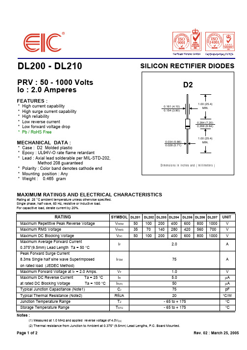
UNIT V V V A
IFSM VF IR IR(H) CJ RθJA TJ TSTG
75 1.0 5.0 50 75 20 - 65 to + 175 - 65 to + 175
A V µA µA pF °C/W °C °C
Typical Junction Capacitance (Note1)
MAXIMUM RATINGS AND ELECTRICAL CHARACTERISTICS
RATING
Maximum Repetitive Peak Reverse Voltage Maximum RMS Voltage Maximum DC Blocking Voltage Maximum Average Forward Current 0.375"(9.5mm) Lead Length Ta = 50 °C Peak Forward Surge Current 8.3ms Single half sine wave Superimposed on rated load (JEDEC Method) Maximum Forward Voltage at IF = 2.0 Amps. Maximum DC Reverse Current at rated DC Blocking Voltage Typical Thermal Resistance (Note2) Junction Temperature Range Storage Temperature Range Notes : Ta = 25 °C Ta = 100 °C
1.6
1.2
45
0.8
30
0.4 RESISTIVE OR INDUCTIVE LOAD 0
sn65hvd230dr中文资料
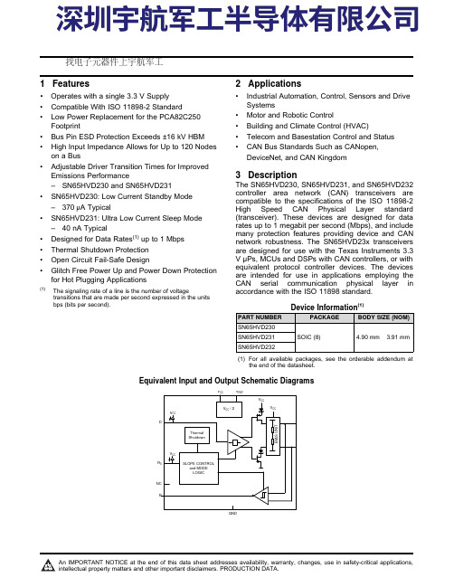
1Features•Operates with a single3.3V Supply •Compatible With ISO11898-2Standard•Low Power Replacement for the PCA82C250 Footprint•Bus Pin ESD Protection Exceeds±16kV HBM •High Input Impedance Allows for Up to120Nodes on a Bus•Adjustable Driver Transition Times for Improved Emissions Performance–SN65HVD230and SN65HVD231•SN65HVD230:Low Current Standby Mode –370μA Typical•SN65HVD231:Ultra Low Current Sleep Mode –40nA Typical•Designed for Data Rates(1)up to1Mbps •Thermal Shutdown Protection•Open Circuit Fail-Safe Design•Glitch Free Power Up and Power Down Protection for Hot Plugging Applications(1)The signaling rate of a line is the number of voltagetransitions that are made per second expressed in the unitsbps(bits per second).2Applications•Industrial Automation,Control,Sensors and Drive Systems•Motor and Robotic Control•Building and Climate Control(HVAC)•Telecom and Basestation Control and Status •CAN Bus Standards Such as CANopen,DeviceNet,and CAN Kingdom3DescriptionThe SN65HVD230,SN65HVD231,and SN65HVD232 controller area network(CAN)transceivers are compatible to the specifications of the ISO11898-2 High Speed CAN PhysicalLayer standard(transceiver).These devices are designed for datarates up to1megabit per second(Mbps),and includemany protection features providing device and CANnetwork robustness.The SN65HVD23x transceiversare designed for use with the Texas Instruments3.3VµPs,MCUs and DSPs with CAN controllers,or withequivalent protocol controller devices.The devicesare intended for use in applications employing theCAN serial communication physical layer inaccordance with the ISO11898standard.Device Information(1)PART NUMBER PACKAGE BODY SIZE(NOM)SN65HVD230SOIC(8) 4.90mm×3.91mmSN65HVD231SN65HVD232(1)For all available packages,see the orderable addendum atthe end of the datasheet.Equivalent Input and Output Schematic Diagrams找电子元器件上宇航军工GND3SN65HVD230,SN65HVD231,SN65HVD232SLOS346O –MARCH 2001–REVISED APRIL 2018Submit Documentation Feedback Copyright ©2001–2018,Texas Instruments Incorporated Changes from Revision J (January 2009)to Revision K Page•Replaced the DISSIPATION RATING TABLE with the Thermal Information table (6)Changes from Revision I (October 2007)to Revision J Page•Deleted Low-to-High Propagation Delay Time vs Common-Mode Input Voltage Characteristics .......................................12•Deleted Driver Schematic Diagram......................................................................................................................................12•Added Figure 38...................................................................................................................................................................32V CC34SN65HVD230,SN65HVD231,SN65HVD232SLOS346O –MARCH 2001–REVISED APRIL 2018Submit Documentation Feedback Copyright ©2001–2018,Texas Instruments Incorporated13.2Layout ExampleFigure 44.SN65HVD23x Board LayoutIMPORTANT NOTICE AND DISCLAIMERTI PROVIDES TECHNICAL AND RELIABILITY DATA(INCLUDING DATASHEETS),DESIGN RESOURCES(INCLUDING REFERENCE DESIGNS),APPLICATION OR OTHER DESIGN ADVICE,WEB TOOLS,SAFETY INFORMATION,AND OTHER RESOURCES“AS IS”AND WITH ALL FAULTS,AND DISCLAIMS ALL WARRANTIES,EXPRESS AND IMPLIED,INCLUDING WITHOUT LIMITATION ANY IMPLIED WARRANTIES OF MERCHANTABILITY,FITNESS FOR A PARTICULAR PURPOSE OR NON-INFRINGEMENT OF THIRD PARTY INTELLECTUAL PROPERTY RIGHTS.These resources are intended for skilled developers designing with TI products.You are solely responsible for(1)selecting the appropriate TI products for your application,(2)designing,validating and testing your application,and(3)ensuring your application meets applicable standards,and any other safety,security,or other requirements.These resources are subject to change without notice.TI grants you permission to use these resources only for development of an application that uses the TI products described in the resource.Other reproduction and display of these resources is prohibited.No license is granted to any other TI intellectual property right or to any third party intellectual property right.TI disclaims responsibility for,and you will fully indemnify TI and its representatives against,any claims, damages,costs,losses,and liabilities arising out of your use of these resources.TI’s products are provided subject to TI’s Terms of Sale()or other applicable terms available either on ti.or provided in conjunction with such TI products.TI’s provision of these resources does not expand or otherwise alter TI’s applicable warranties or warranty disclaimers for TI products.Mailing Address:Texas Instruments,Post Office Box655303,Dallas,Texas75265Copyright© 2020,Texas Instruments Incorporated。
SN65HVD07中文资料

ORDERING INFORMATION SIGNALINGIMPORTANT NOTICETexas Instruments Incorporated and its subsidiaries (TI) reserve the right to make corrections, modifications, enhancements, improvements, and other changes to its products and services at any time and to discontinue any product or service without notice. Customers should obtain the latest relevant information before placing orders and should verify that such information is current and complete. All products are sold subject to TI’s terms and conditions of sale supplied at the time of order acknowledgment.TI warrants performance of its hardware products to the specifications applicable at the time of sale in accordance with TI’s standard warranty. T esting and other quality control techniques are used to the extent TI deems necessary to support this warranty. Except where mandated by government requirements, testing of all parameters of each product is not necessarily performed.TI assumes no liability for applications assistance or customer product design. Customers are responsible for their products and applications using TI components. T o minimize the risks associated with customer products and applications, customers should provide adequate design and operating safeguards.TI does not warrant or represent that any license, either express or implied, is granted under any TI patent right, copyright, mask work right, or other TI intellectual property right relating to any combination, machine, or process in which TI products or services are used. Information published by TI regarding third-party products or services does not constitute a license from TI to use such products or services or a warranty or endorsement thereof. Use of such information may require a license from a third party under the patents or other intellectual property of the third party, or a license from TI under the patents or other intellectual property of TI.Reproduction of information in TI data books or data sheets is permissible only if reproduction is without alteration and is accompanied by all associated warranties, conditions, limitations, and notices. Reproduction of this information with alteration is an unfair and deceptive business practice. TI is not responsible or liable for such altered documentation.Resale of TI products or services with statements different from or beyond the parameters stated by TI for that product or service voids all express and any implied warranties for the associated TI product or service and is an unfair and deceptive business practice. TI is not responsible or liable for any such statements. Following are URLs where you can obtain information on other Texas Instruments products and application solutions:Products ApplicationsAmplifiers Audio /audioData Converters Automotive /automotiveDSP Broadband /broadbandInterface Digital Control /digitalcontrolLogic Military /militaryPower Mgmt Optical Networking /opticalnetwork Microcontrollers Security /securityTelephony /telephonyVideo & Imaging /videoWireless /wirelessMailing Address:Texas InstrumentsPost Office Box 655303 Dallas, Texas 75265Copyright 2004, Texas Instruments Incorporated。
SN65DP141 DisplayPort线性转接驱动器说明书

SN65DP141 DisplayPort 线性转接驱动器1 特性•支持 VESA DisplayPort 1.4a 、2.0 和 eDP 1.4•四通道线性转接驱动器,支持高达 12Gbps 的数据速率,包括 DisplayPort RBR 、HBR 、HBR2、HBR3 和 UHBR10•与协议无关•透明呈现 DP 链路训练•与在链路上的位置无关,适用于源端、接收端和电缆应用•6GHz 时模拟均衡为 15dB •输出线性动态范围:1200mV •带宽:>20 GHz•6GHz 时的回波损耗优于 16dB • 2.5V 或 3.3V ±5% 单电源选项•低功耗,2.5V V CC 时每通道 80mW •GPIO 或 I 2C 控制2 应用•平板电脑•笔记本电脑•台式机•扩展坞3 说明SN65DP141 是一款与协议无关的异步、低延迟、四通道线性均衡器,该器件经过优化适用于高达 12Gbps 的数据速率并且可对电路板走线和电缆所产生的损耗进行补偿。
该器件透明呈现 DisplayPort (DP) 链路训练,这使得 DP 发送设备和接收设备能够执行有效的链路训练,克服了传统 aux snooping 转接驱动器的缺点。
此外,该器件与位置无关。
它可置于源设备、电缆或接收设备内,从而为总体链路预算有效提供负损耗 分量。
SN65DP141 内的线性均衡在与接收器搭配使用时还可提高链路裕度,从而实现判决反馈均衡 (DFE)。
SN65DP141 支持采用 I 2C 和 GPIO 配置对均衡、增益、动态范围进行独立通道控制。
(1)(1)如需了解所有可用封装,请参阅数据表末尾的可订购产品附录。
GPU DP141DP141Copyright © 2016, Texas Instruments Incorporated简化版原理图Table of Contents1 特性...................................................................................12 应用...................................................................................13 说明...................................................................................14 Revision History ..............................................................25 Pin Configuration and Functions ...................................36 Specifications ..................................................................56.1 Absolute Maximum Ratings........................................56.2 ESD Ratings...............................................................56.3 Recommended Operating Conditions.........................56.4 Thermal Information....................................................66.5 Electrical Characteristics.............................................66.6 Switching Characteristics............................................86.7 Switching Characteristics, I 2C Interface......................96.8 Typical Characteristics..............................................107 Parameter Measurement Information ..........................118 Detailed Description ......................................................158.1 Overview...................................................................158.2 Functional Block Diagram.. (15)8.3 Feature Description...................................................168.4 Device Functional Modes..........................................178.5 Register Maps...........................................................189 Application and Implementation ..................................249.1 Application Information.............................................249.2 Typical Application....................................................2410 Power Supply Recommendations ..............................2611 Layout ...........................................................................2711.1 Layout Guidelines...................................................2711.2 Layout Example......................................................2812 Device and Documentation Support ..........................2912.1 接收文档更新通知...................................................2912.2 支持资源..................................................................2912.3 Trademarks.............................................................2912.4 Electrostatic Discharge Caution..............................2912.5 术语表.....................................................................2913 Mechanical, Packaging, and OrderableInformation (29)4 Revision History注:以前版本的页码可能与当前版本的页码不同Changes from Revision B (September 2021) to Revision C (December 2021)Page•Changed the I2C_EN pin Type from internal pull-up to internal pull-down ........................................................3Changes from Revision A (October 2016) to Revision B (September 2021)Page•更新了整个文档中的表格、图和交叉参考的编号格式.........................................................................................1•将特性从:“支持 VESA DisplayPort 1.3 和 eDP 1.4”更新为:“支持 VESA DisplayPort 1.4a 、2.0 和 eDP 1.4”...................................................................................................................................................................1•将特性从“包括 DisplayPort RBR 、HBR 、HBR2 和 HBR3”更新为“包括 DisplayPort RBR 、HBR 、HBR2、HBR3 和 UHBR10”...........................................................................................................................................1•Updated the DP bit rates from: RBR to HBR3 (1.6 Gbps, 2.7 Gbps, 5.4 Gbps and 8.1 Gbps ... to: RBR toUHBR10 (1.6 Gbps, 2.7 Gbps, 5.4 Gbps, 8.1 Gbps and 10.0 Gbps … in the Overview section......................15•Updated Operating data rate from HBR3 (8.1 Gbps) to UHBR10 (10 Gbps)...................................................24Changes from Revision * (February 2016) to Revision A (October 2016)Page•Replaced 图 9-2 (25)SN65DP141ZHCSEQ7C – FEBRUARY 2016 – REVISED DECEMBER 20215 Pin Configuration and FunctionsThermalPadV C C1IN0_P P W D #2IN0_N R X _G A I N3VCC E Q _M O D E /_A D D 24IN1_P E Q 0/A D D 05IN1_N E Q 1/A D D 16VCC 7VCC OUT0_P 8IN2_P 9IN2_N V C COUT0_N VCC OUT1_P OUT1_N VCC VCC OUT2_P OUT2_N VCC OUT3_P OUT3_NV C CV C CVCC IN3_P IN3_NS D AD R V _P K #/S C LI 2C _E NT X _D C _G A I N /C SR E X T1011121314151617181920212223242526272829303132333435363738It is required for the thermal pad to be soldered to ground for better thermal performance.图 5-1. RLJ Package 38 Pins (WQFN) Top ViewSN65DP141ZHCSEQ7C – FEBRUARY 2016 – REVISED DECEMBER 2021SN65DP141ZHCSEQ7C – FEBRUARY 2016 – REVISED DECEMBER (1)I = input, O = output6 Specifications6.1 Absolute Maximum Ratings(1)(2)(1)Stresses beyond those listed under Absolute Maximum Ratings may cause permanent damage to the device. These are stress ratings only, which do not imply functional operation of the device at these or any other conditions beyond those indicated underRecommended Operating Conditions . Exposure to absolute-maximum-rated conditions for extended periods may affect device reliability.(2)All voltage values, except differential I/O bus voltages, are with respect to network ground terminal.6.2 ESD Ratings(1)JEDEC document JEP155 states that 500-V HBM allows safe manufacturing with a standard ESD control process.(2)JEDEC document JEP157 states that 250-V CDM allows safe manufacturing with a standard ESD control process. .6.3 Recommended Operating ConditionsSN65DP141ZHCSEQ7C – FEBRUARY 2016 – REVISED DECEMBER 2021SN65DP141ZHCSEQ7C – FEBRUARY 2016 – REVISED DECEMBER 6.4 Thermal Information(1)For more information about traditional and new thermal metrics, see the Semiconductor and IC Package Thermal Metrics applicationreport, SPRA953.6.5 Electrical Characteristics6.5 Electrical Characteristics (continued)SN65DP141ZHCSEQ7C – FEBRUARY 2016 – REVISED DECEMBER 2021SN65DP141ZHCSEQ7C – FEBRUARY 2016 – REVISED DECEMBER 6.6 Switching Characteristics(1)Rise and Fall measurements include board and channel effects of the test environment, refer to 图 7-1 and 图 7-3.(2)t SK(O) is the magnitude of the time difference between the channels.(3)t SK(PP) is the magnitude of the difference in propagation delay times between any specified terminals of two devices when both devicesoperate with the same(4)All noise sources added.6.7 Switching Characteristics, I 2C InterfaceSN65DP141ZHCSEQ7C – FEBRUARY 2016 – REVISED DECEMBER 20216.8 Typical Characteristics−45−40−35−30−25−20−15−10−5002468101214Frequency (GHz)A m p l i t u d e (dB )图 6-1. Differential Input Return Loss−70−60−50−40−30−20−1002468101214Frequency (GHz)A m p l i t u d e (dB )图 6-2. Differential to Common Mode Conversion−40−35−30−25−20−15−10−5002468101214Frequency (GHz)A m p l i t u d e (dB )图 6-3. Differential Output Return Loss −45−40−35−30−25−20−15−10−5002468101214Frequency (GHz)A m p l i t u d e (dB )图 6-4. Common Mode Output Return LossSN65DP141ZHCSEQ7C – FEBRUARY 2016 – REVISED DECEMBER 20217 Parameter Measurement InformationCopyright © 2016, Texas Instruments Incorporated图 7-1. Common Mode Output Voltage Test Circuit图 7-2. Propagation Delay Input to Output图 7-3. Output Rise and Fall TimesOUTxOUT y图 7-4. Output Inter-Pair Skew0V图 7-5. V (pre) and V (post) (test pattern is 1111111100000000 (8-1s, 8-0s))CHARACTERIZATION TEST CHANNEL图 7-6. Receive Side Performance Test Circuit图 7-7. Transmit Side Performance Test CircuitIN-Copyright © 2016, Texas Instruments Incorporated图 7-8. Equivalent Input CircuitINCopyright © 2016, Texas Instruments Incorporated图 7-9. 3-Level Input Biasing Network图 7-10. Two – Wire Serial Interface Data Transfer图 7-11. Two – Wire Serial Interface Timing Diagram8 Detailed Description8.1 OverviewThe SN65DP141 is an asynchronous, protocol-agnostic, low latency, four-channel linear equalizer optimized for use up to 12 Gbps. The characteristics of this device make it transparent to DisplayPort (DP) link training. It supports all the available DP bit rates from RBR to UHBR10 (1.6 Gbps, 2.7 Gbps, 5.4 Gbps, 8.1 Gbps, and 10.0 Gbps respectively). Additionally, the SN65DP141 is configurable to a trace or cable mode, and hence improves its performance depending on the type of channel it is being used. Its transparency to the DP link training makes the SN65DP141 a position independent device, suitable for source/sink or cable applications, effectively providing a negative loss component to the overall link budget, in order to compensate the signal degradation over the channel.The SN65DP141 is configurable by means of I 2C and GPIOs, allowing independent channel control for activation, equalization, gain, and dynamic range.8.2 Functional Block DiagramGNDIN[3:0]_P DRV_PK#/SCLSDA VOD/CS GAININ[3:0]_NCopyright © 2016, Texas Instruments Incorporated8.3 Feature Description8.3.1 DC and AC Independent Gain ControlBesides the functional block diagram, the behavior of the SN65DP141 can be described as it is shown in 图 8-1; where the input stage first applies a DC gain (0 dB or –6 dB) and then equalizes the signal, which is driven to the output stage where the SN65DP141 applies an output DC gain (0 dB or 6 dB).TX_GAIN(TX_DC_GAIN)EQUALIZATION(EQ_AC_GAIN)RX_GAIN(EQ_DC_GAIN)0dB or -6dB Up to 15dB0dB or 6dB图 8-1. DP141 Signal Chain Gain Control8.3.2 Two-Wire Serial Interface and Control LogicThe SN65DP141 uses a 2-wire serial interface for digital control. The two circuit inputs, SDA and SCL, are driven, respectively, by the serial data and serial clock from a microcontroller, for example. The SDA and SCK pins require external 10 kΩ pull-ups to VCC.The 2-wire interface allows write access to the internal memory map to modify control registers and read access to read out control and status signals. The SN65DP141 is a slave device only which means that it cannot initiate a transmission itself; it always relies on the availability of the SCK signal for the duration of the transmission. The master device provides the clock signal as well as the START and STOP commands. The protocol for a data transmission is as follows:1.START command2.7 bit slave address (0000ADD [2:0]) followed by an eighth bit which is the data direction bit (R/W). A zeroindicates a WRITE and a 1 indicates a READ. The ADD [2:0] address bits change with the status of the ADD2, ADD1, and ADD0 device pins, respectively. If the pins are left floating or pulled down, the 7 bit slave address is 0000000.3.8-bit register address4.8-bit register data word5.STOP commandRegarding timing, the SN65DP141 is I2C compatible. The typical timing is shown in 图 7-11 and a complete data transfer is shown in 图7-10. Parameters for these figures are defined in the I2C Interface section of the Switching Characteristics.8.3.3 Bus IdleBoth SDA and SCL lines remain HIGH8.3.4 Start Data TransferA change in the state of the SDA line, from HIGH to LOW, while the SCL line is HIGH, defines a START condition (S). Each data transfer is initiated with a START condition.8.3.5 Stop Data TransferA change in the state of the SDA line from LOW to HIGH while the SCL line is HIGH defines a STOP condition (P). Each data transfer is terminated with a STOP condition; however, if the master still wishes to communicate on the bus, it can generate a repeated START condition and address another slave without first generating a STOP condition.8.3.6 Data TransferThe number of data bytes transferred between a START and a STOP condition is not limited and is determined by the master device. The receiver acknowledges the transfer of data.8.3.7 AcknowledgeEach receiving device, when addressed, is obliged to generate an acknowledge bit. The transmitter releases the SDA line and a device that acknowledges must pull down the SDA line during the acknowledge clock pulse in such a way that the SDA line is stable LOW during the HIGH period of the acknowledge clock pulse. Setup and hold times must be taken into account. When a slave-receiver doesn’t acknowledge the slave address, the data line must be left HIGH by the slave. The master can then generate a STOP condition to abort the transfer. If the slave-receiver does acknowledge the slave address but some time later in the transfer cannot receive any more data bytes, the master must abort the transfer. This is indicated by the slave generating the not acknowledge on the first byte to follow. The slave leaves the data line HIGH and the master generates the STOP condition.8.4 Device Functional Modes8.4.1 TRACE and CABLE Equalization ModesThe SN65DP141 is optimized for both trace and cable application at its input. The device pin EQ_MODE sets the EQ gain curve profile suitable for these two use cases.8.4.2 Control ModesThe SN65DP141 features two control modes: GPIO and I2C, and the selection between these two modes is by means of the I2C_EN terminal, which activates the GPIO when tied to LOW; otherwise, the I2C mode is active due to its internal pull-up resistance.8.4.3 GPIO MODEDevice Pins RX_GAIN, EQ1 and EQ0 determines receiver DC and AC gain as shown in 表 8-1 and 表 8-2.8.4.4 I2C Mode8.5 Register Maps8.5.1 Register 0x00 (General Device Settings) (offset = 00000000) [reset = 00000000]LEGEND: R/W = Read/Write; R = Read only; -n = value after reset8.5.2 Register 0x01 (Channel Enable) (offset = 00000000) [reset = 00000000]LEGEND: R/W = Read/Write; R = Read only; -n = value after reset8.5.3 Register 0x02 (Channel 0 Control Settings) (offset = 00000000) [reset = 00000000]LEGEND: R/W = Read/Write; R = Read only; -n = value after reset8.5.4 Register 0x03 (Channel 0 Enable Settings) (offset = 00000000) [reset = 00000000]LEGEND: R/W = Read/Write; R = Read only; -n = value after reset8.5.5 Register 0x05 (Channel 1 Control Settings) (offset = 00000000) [reset = 00000000]LEGEND: R/W = Read/Write; R = Read only; -n = value after reset8.5.6 Register 0x06 (Channel 1 Enable Settings) (offset = 00000000) [reset = 00000000]LEGEND: R/W = Read/Write; R = Read only; -n = value after resetSN65DP141ZHCSEQ7C – FEBRUARY 2016 – REVISED DECEMBER 2021SN65DP141ZHCSEQ7C – FEBRUARY 2016 – REVISED DECEMBER 8.5.7 Register 0x08 (Channel 2 Control Settings) (offset = 00000000) [reset = 00000000]LEGEND: R/W = Read/Write; R = Read only; -n = value after reset8.5.8 Register 0x09 (Channel 2 Enable Settings) (offset = 00000000) [reset = 00000000]LEGEND: R/W = Read/Write; R = Read only; -n = value after reset8.5.9 Register 0x0B (Channel 3 Control Settings) (offset = 00000000) [reset = 00000000]LEGEND: R/W = Read/Write; R = Read only; -n = value after reset8.5.10 Register 0x0C (Channel 3 Control Settings) (offset = 00000000) [reset = 00000000]LEGEND: R/W = Read/Write; R = Read only; -n = value after resetSN65DP141ZHCSEQ7C – FEBRUARY 2016 – REVISED DECEMBER 20219 Application and Implementation备注以下应用部分中的信息不属于TI 器件规格的范围,TI 不担保其准确性和完整性。
D202RW资料
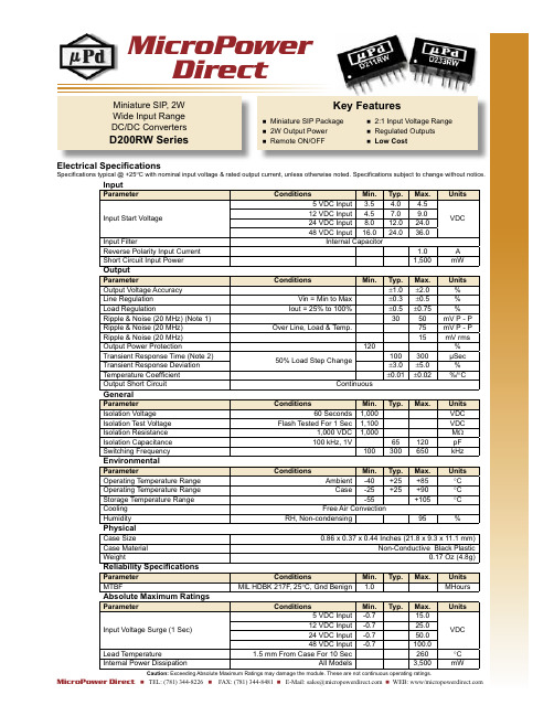
Key FeaturesMiniature SIP Package 2:1 Input Voltage Range 2W Output Power Regulated Outputs Remote ON/OFFLow CostElectrical Specifi cationsSpecifi cations typical @ +251C with nominal input voltage & rated output current, unless otherwise noted. Specifi cations subject to change without notice.MicroPowerDirectMiniature SIP , 2W Wide Input Range DC/DC ConvertersD200RW SeriesMicroPower Direct TEL: (781) 344-8226 FAX: (781) 344-8481 E-Mail: sales@WEB: www/InputParameter ConditionsMin.Typ.Max.Units Input Start Voltage5 VDC Input 3.5 4.0 4.5VDC12 VDC Input 4.57.09.024 VDC Input 8.012.024.048 VDC Input 16.024.036.0Input FilterInternal CapacitorReverse Polarity Input Current 1.0A Short Circuit Input Power1,500mW OutputParameterConditionsMin.Typ.Max.Units Output Voltage Accuracy ±1.0±2.0%Line Regulation Vin = Min to Max ±0.3±0.5%Load RegulationIout = 25% to 100%±0.5±0.75%Ripple & Noise (20 MHz) (Note 1)3050mV P - P Ripple & Noise (20 MHz)Over Line, Load & Temp.75mV P - P Ripple & Noise (20 MHz)15mV rms Output Power Protection120%Transient Response Time (Note 2)50% Load Step Change100300µSec Transient Response Deviation ±3.0±5.0%Temperature Coeffi cient ±0.01±0.02%/°COutput Short CircuitContinuousGeneralParameterConditionsMin.Typ.Max.Units Isolation Voltage60 Seconds1,000VDC Isolation Test Voltage Flash Tested For 1 Sec1,100VDC Isolation Resistance 1,000 VDC 1,000M ΩIsolation Capacitance 100 kHz, 1V65120pF Switching Frequency100300650kHz EnvironmentalParameterConditionsMin.Typ.Max.Units Operating Temperature Range Ambient -40+25+85°C Operating Temperature Range Case -25+25+90°C Storage Temperature Range -55+105°C Cooling Free Air ConvectionHumidityRH, Non-condensing95%PhysicalCase Size 0.86 x 0.37 x 0.44 Inches (21.8 x 9.3 x 11.1 mm)Case Material Non-Conductive Black PlasticWeight0.17 Oz (4.8g)Reliability Specifi cationsParameter ConditionsMin.Typ.Max.Units MTBFMIL HDBK 217F, 25°C, Gnd Benign1.0MHours Absolute Maximum RatingsParameterConditionsMin.Typ.Max.Units Input Voltage Surge (1 Sec) 5 VDC Input -0.715.0VDC 12 VDC Input -0.725.024 VDC Input -0.750.048 VDC Input-0.7100.0Lead Temperature1.5 mm From Case For 10 Sec260°C Internal Power DissipationAll Models3,500mWCaution: Exceeding Absolute Maximum Ratings may damage the module. These are not continuous operating ratings.。
sn65hvd230中文用户手册

13.1 布局布线指南......................................................... 31 13.2 布局示例................................................................ 31 14 器件和文档支持 ..................................................... 32 14.1 相关链接................................................................ 32 14.2 商标 ....................................................................... 32 14.3 静电放电警告......................................................... 32 14.4 术语表 ................................................................... 32 15 机械、封装和可订购信息....................................... 32
Product Folder
Sample & Buy
Technical Documents
SN65HVD12中文资料
ORDERING INFORMATION SIGNALING RATEDriver InputDriver OutputReceiver InputReceiver Output Figure 22. HVD12 Input and Output Through 2000 Feet of CableAn example application for the HVD12 is illustrated inHVD12 transceivers are used to communicate data through a 2000 foot (600 m) length of Commscope 5524 category 5e+ twisted pair cable. The bus is terminated at each end by a 100-matching the cable characteristic impedance. Figure 22 illustrates operation at a signaling rate of 250 kbps.IMPORTANT NOTICETexas Instruments Incorporated and its subsidiaries (TI) reserve the right to make corrections, modifications, enhancements, improvements, and other changes to its products and services at any time and to discontinue any product or service without notice. Customers should obtain the latest relevant information before placing orders and should verify that such information is current and complete. All products are sold subject to TI’s terms and conditions of sale supplied at the time of order acknowledgment.TI warrants performance of its hardware products to the specifications applicable at the time of sale in accordance with TI’s standard warranty. T esting and other quality control techniques are used to the extent TI deems necessary to support this warranty. Except where mandated by government requirements, testing of all parameters of each product is not necessarily performed.TI assumes no liability for applications assistance or customer product design. Customers are responsible for their products and applications using TI components. T o minimize the risks associated with customer products and applications, customers should provide adequate design and operating safeguards.TI does not warrant or represent that any license, either express or implied, is granted under any TI patent right, copyright, mask work right, or other TI intellectual property right relating to any combination, machine, or process in which TI products or services are used. Information published by TI regarding third-party products or services does not constitute a license from TI to use such products or services or a warranty or endorsement thereof. Use of such information may require a license from a third party under the patents or other intellectual property of the third party, or a license from TI under the patents or other intellectual property of TI.Reproduction of information in TI data books or data sheets is permissible only if reproduction is without alteration and is accompanied by all associated warranties, conditions, limitations, and notices. Reproduction of this information with alteration is an unfair and deceptive business practice. TI is not responsible or liable for such altered documentation.Resale of TI products or services with statements different from or beyond the parameters stated by TI for that product or service voids all express and any implied warranties for the associated TI product or service and is an unfair and deceptive business practice. TI is not responsible or liable for any such statements. Following are URLs where you can obtain information on other Texas Instruments products and application solutions:Products ApplicationsAmplifiers Audio /audioData Converters Automotive /automotiveDSP Broadband /broadbandInterface Digital Control /digitalcontrolLogic Military /militaryPower Mgmt Optical Networking /opticalnetwork Microcontrollers Security /securityTelephony /telephonyVideo & Imaging /videoWireless /wirelessMailing Address:Texas InstrumentsPost Office Box 655303 Dallas, Texas 75265Copyright 2004, Texas Instruments Incorporated。
LVDS

LVDS2010-08-25 21:41:18| 分类:论文| 标签:|字号大中小订阅今天接到了一个TI的电路(SN65LVDT352)要求测试,以前没有接触过,今天在网上收集点资料, 拿来和大家分享.以后可能会用的上这种器件.LVDS:Low Voltage Differential Signaling,低电压差分信号。
LVDS传输支持速率一般在155Mbps(大约为77MHZ)以上。
LVDS是一种低摆幅的差分信号技术,它使得信号能在差分PCB线对或平衡电缆上以几百Mbps 的速率传输,其低压幅和低电流驱动输出实现了低噪声和低功耗。
IEEE在两个标准中对LVDS信号进行了定义。
ANSI/TIA/EIA-644中,推荐最大速率为655Mbps,理论极限速率为1.923Mbps。
1.1 LVDS信号传输组成LVDS信号传输一般由三部分组成:差分信号发送器,差分信号互联器,差分信号接收器。
差分信号发送器:将非平衡传输的TTL信号转换成平衡传输的LVDS信号。
通常由一个IC来完成,如:DS90C031差分信号接收器:将平衡传输的LVDS信号转换成非平衡传输的TTL信号。
通常由一个IC来完成,如:DS90C032差分信号互联器:包括联接线(电缆或者PCB走线),终端匹配电阻。
按照IEEE规定,电阻为100欧。
我们通常选择为100,120欧。
1.2 LVDS信号电平特性LVDS物理接口使用1.2V偏置电压作为基准,提供大约400mV摆幅。
LVDS驱动器由一个驱动差分线对的电流源组成(通常电流为3.5mA),LVDS接收器具有很高的输入阻抗,因此驱动器输出的电流大部分都流过100Ω的匹配电阻,并在接收器的输入端产生大约350mV 的电压。
电流源为恒流特性,终端电阻在100――120欧姆之间,则电压摆动幅度为:3.5mA * 100 =350mV ;3.5mA * 120 = 420mV 。
LVDS与PECL(光收发器使用的电平)电平变化。
WB202资料

PARAMETER (TEST CONDITIONS)
Series Number Maximum DC Blocking Voltage Maximum RMS Voltage Maximum Peak Recurrent Reverse Voltage Average Forward Rectified Current @ TA = 25 oC Peak Forward Surge Current (8.3mS single half sine wave superimposed on rated load) Maximum Forward Voltage (Per Diode) at 1 Amp DC Maximum Average DC Reverse Current At Rated DC Blocking Voltage Operating and Storage Temperature Range @ TA = 25 C o @ TA = 100 C
B B1 B1 + AC _
MILLIMETERS SYM
Terminals: Round silver plated pins
Soldering: Per MIL-STD 202 Method 208 guaranteed
+
INCHES MIN 0.340 0.030 0.180 0.200 1.20 1.0 MAX 0.350 0.032 0.220 0.220 n/a n/a
MECHANICAL SPECIFICATION
ACTUAL SIZE OF WB PACKAGE
SERIES WB200 - WB210
Surge overload rating to 60 Amps peak
SN65HVD1794中文资料

CABLE LENGTH 1500 m 150 m 50 m
1
Please be aware that an important notice concerning availability, standard warranty, and use in critical applications of Texas Instruments semiconductor products and disclaimers thereto appears at the end of this data sheet.
H
Receive inverted bus High
H
Fail-safe high output
L
Failsafe inverted output
H
Fail-safe high output
L
Failsafe inverted output
H
Fail-safe high output
L
Failsafe inverted output
INV Input Can Correct for Crossed Wires
VFAULT up to 70 V
PART NUMBER SN65HVD1794 SN65HVD1795 PREVIEW SN65HVD1796 PREVIEW
PRODUCT SELECTION GUIDE
DUPLEX Half Half Half
ABSOLUTE MAXIMUM RATINGS(1)
VCC Supply voltage Voltage range at A and B pins Input voltage range at any logic pin Voltage input range, transient pulse, A and B, through 100 Ω Receiver output current
SN65HVD233MDREP中文资料

This device has limited built-in ESD protection. The leads should be shorted together or the device placed in conductive foam duቤተ መጻሕፍቲ ባይዱing storage or handling to prevent electrostatic damage to the MOS gates.
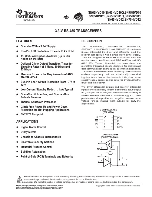
3.3-V CAN TRANSCEIVER
1
FEATURES
Bus-Pin Fault Protection Exceeds ±36 V Bus-Pin ESD Protection Exceeds 16-kV HBM Compatible With ISO 11898 Signaling Rates(1) up to 1 Mbps Extended –7-V to 12-V Common-Mode Range High-Input Impedance Allows for 120 Nodes LVTTL I/Os Are 5-V Tolerant Adjustable Driver Transition Times for Improved Signal Quality Unpowered Node Does Not Disturb the Bus Low-Current Standby Mode . . . 200-µA Typical Thermal Shutdown Protection Power-Up/Down Glitch-Free Bus Inputs and Outputs – High Input Impedance With Low VCC – Monolithic Output During Power Cycling Loopback for Diagnostic Functions Available DeviceNet Vendor ID #806
SN65HVD08D中文资料

FEATURESAPPLICATIONSDESCRIPTIONV CCBAGNDD or P PACKAGE(TOP VIEW)LOGIC DIAGRAM (Positive Logic)DADERERBRemote(One of n Shown)SN75HVD08,SN65HVD08SLLS550A–NOVEMBER2002–REVISED MAY2003 WIDE SUPPLY RANGE RS-485TRANSCEIVERThe wide supply voltage range and low quiescentcurrent requirements allow the SN65HVD08s to •Operates With a3-V to5.5-V Supplyoperate from a5-V power bus in the cable with as •Consumes Less Than90mW Quiescent much as a2-V line voltage drop.Busing power in the Power cable can alleviate the need for isolated power to begenerated at each connection of a ground-isolated •Open-Circuit,Short Circuit,and Idle-Busbus.Failsafe Receiver•1/8th Unit-Load(up to256nodes on the bus)The driver differential outputs and receiver differentialinputs connect internally to form a differential in-•Bus-Pin ESD Protection Exceeds16kV HBMput/output(I/O)bus port that is designed to offer •Driver Output Voltage Slew-Rate Limited for minimum loading to the bus whenever the driver is Optimum Signal Quality at10Mbps disabled or not powered.The drivers and receivers •Electrically Compatible With ANSI TIA/EIA-485have active-high and active-low enables respectively,which can be externally connected together to func-Standardtion as a direction control.•Data Transmission With Remote StationsPowered From the Host•Isolated Multipoint Data Buses•Industrial Process Control Networks•Point-of-Sale Networks•Electric Utility MeteringThe SN65HVD08combines a3-state differential linedriver and differential line receiver designed for bal-anced data transmission and interoperation with ANSITIA/EIA-485-A and ISO-8482E standard-compliantdevices.Please be aware that an important notice concerning availability,standard warranty,and use in critical applications of TexasInstruments semiconductor products and disclaimers thereto appears at the end of this data sheet.These devices have limited built-in ESD protection.The leads should be shorted together or the device placed in conductive foam during storage or handling to prevent electrostatic damage to the MOS gates.ORDERING INFORMATIONover operating free-air temperature range unless otherwise noted(1)(2)(1)Stresses beyond those listed under"absolute maximum ratings”may cause permanent damage to the device.These are stress ratingsonly,and functional operation of the device at these or any other conditions beyond those indicated under"recommended operating conditions”is not implied.Exposure to absolute-maximum-rated conditions for extended periods may affect device reliability.(2)All voltage values,except differential I/O bus voltages,are with respect to network ground terminal.(3)Tested in accordance with JEDEC Standard22,Test Method A114-A.(4)Tested in accordance with JEDEC Standard22,Test Method C101.(1)The algebraic convention,in which the least positive(most negative)limit is designated as minimum is used in this data sheet.ELECTRICAL CHARACTERISTICS DRIVER SWITCHING CHARACTERISTICSSN75HVD08,SN65HVD08 SLLS550A–NOVEMBER2002–REVISED MAY2003over recommended operating conditions unless otherwise notedover recommended operating conditions unless otherwise notedRECEIVER SWITCHING CHARACTERISTICSPARAMETER MEASUREMENT INFORMATION0 or 3 V–7 V < V (test) < 12 VInputABV A V B V V OCV Input: PRR = 500 kHz, 50% Duty Cycle,t r <6ns, t f <6ns, Z O = 50 ΩL Instrumentation CapacitanceGenerator: PRR = 500 kHz, 50% Duty Cycle, t r <6 ns, t f <6 ns, Z o = 50 Ω3 V2 V –2 V C L = 50 pF ±20%C L Includes Fixture and Instrumentation CapacitanceSN75HVD08,SN65HVD08SLLS550A–NOVEMBER 2002–REVISED MAY 2003over recommended operating conditions unless otherwise notedFigure 1.Driver V OD With Common-Mode Loading Test CircuitFigure 2.Test Circuit and Definitions for the Driver Common-Mode Output VoltageFigure 3.Driver Switching Test Circuit and Voltage WaveformsR L = 110 Ω ± 1%Generator: PRR = 500 kHz, 50% Duty Cycle, t r <6 ns, t f <6 ns, Z o = 50 ΩOH≈ 0 VV O≈ 3 V0 VV OL Generator: PRR = 500 kHz, 50% Duty Cycle, t r <6 ns, t f<6 ns, Z o = 50 ΩΩ ≈3 V Generator: PRR = 500 kHz, 50% Duty Cycle, t r <6 ns, t f <6 ns, Z o = 50 Ω3 VV OHVOLC L = 15 pF ±20%C L Includes Fixture and Instrumentation Capacitance0 V SN75HVD08,SN65HVD08SLLS550A–NOVEMBER 2002–REVISED MAY 2003Parameter Measurement Information (continued)Figure 4.Driver High-Level Enable and Disable Time Test Circuit and Voltage WaveformsFigure 5.Driver Low-Level Output Enable and Disable Time Test Circuit and Voltage WaveformsFigure 6.Receiver Switching Test Circuit and Voltage WaveformsGenerator: PRR = 500 kHz, 50% Duty Cycle, t r <6 ns, t f <6 ns, Z o = 50 Ω0 V or 3 VA BD at 3 V S1 to B≈ V CCV OLD at 0 V S1 to ASN75HVD08,SN65HVD08SLLS550A–NOVEMBER 2002–REVISED MAY 2003Parameter Measurement Information (continued)Figure 7.Receiver Enable and Disable Time Test Circuit and Voltage Waveforms With Drivers EnabledGenerator: PRR = 100 kHz, 50% Duty Cycle, t r <6 ns, t f <6 ns, Z o = 50 ΩV A BA at 1.5 VB at 0 VS1 to BV OLV A at 0 V B at 1.5 V S1 to A ≈ V CCDEVICE INFORMATIONSN75HVD08,SN65HVD08SLLS550A–NOVEMBER 2002–REVISED MAY 2003Parameter Measurement Information (continued)Figure 8.Receiver Enable Time From Standby (Driver Disabled)Function TablesDRIVERRECEIVER(1)H =high level;L =low level;Z =high impedance;X =irrelevant;?=indeterminateEQUIVALENT INPUT AND OUTPUT SCHEMATIC DIAGRAMSSN75HVD08,SN65HVD08SLLS550A–NOVEMBER 2002–REVISED MAY 2003TYPICAL CHARACTERISTICS2.521.51D i f f e r e n t i a l O u t p u t V o l t a g e – V33.5DIFFERENTIAL OUTPUT VOLTAGEvsSUPPLY VOLTAGE4V CC – Supply Voltage – VI O – D r i v e r O u t p u t C u r r e n t – m ADRIVER OUTPUT CURRENTvsSUPPLY VOLTAGEV CC – Supply Voltage – V10.502.53.54.5L o g i c I n p u t T h r e s h o l d V o l t a g e – V1.52LOGIC INPUT THRESHOLD VOLTAGEvsSUPPLY VOLTAGE2.55.56.5V CC – Supply Voltage – V4060801001202.557.510Signaling Rate – MbpsRMS SUPPLY CURRENTvsSIGNALING RATEI C C – R M S S u p p l y C u r r e n t – m ASN75HVD08,SN65HVD08SLLS550A–NOVEMBER 2002–REVISED MAY 2003Figure 9.Figure 10.Figure 11.Figure 12.APPLICATION INFORMATIONOPTO-ISOLATED DATA BUSESSUPPLY SOURCE IMPEDANCEV S R LSN75HVD08,SN65HVD08SLLS550A–NOVEMBER 2002–REVISED MAY 2003As electrical loads are physically distanced from their power source,the effects of supply and return line Under dynamic load requirements,the distributed impedance and the resultant voltage drop must be inductance and capacitance of the power lines may accounted.If the supply regulation at the load cannot not be ignored and decoupling capacitance at the be maintained to the circuit requirements,it forces the load is required.The amount depends upon the use of remote sensing,additional regulation at the magnitude and frequency of the load current change load,bigger or shorter cables,or a combination of but,if only powering the SN65HVD08,a 0.1µF these.The SN65HVD08eases this problem by re-ceramic capacitor is usually sufficient.laxing the supply requirements to allow for more variation in the supply voltage over typical RS-485transceivers.Long RS-485circuits can create large ground loops and pick up common-mode noise voltages in excess of the range tolerated by standard RS-485circuits.A In the steady state,the voltage drop from the source common remedy is to provide galvanic isolation of the to the load is simply thewire resistance times the data circuit from earth or local grounds.load current as modeled in Figure 13.Transformers,capacitors,or phototransistors most often provide isolation of the bus and the local node.Transformers and capacitors require changing signals to transfer the information over the isolation barrier and phototransistors (opto-isolators)can pass steady-state signals.Each of these methods incurs additional costs and complexity,the former in clock encoding and decoding of the data stream and the latter in requiring an isolated power supply.Quite often,the cost of isolated power is repeated at Figure 13.Steady-State Circuit Modeleach node connected to the bus as shown in Fig-ure 14.The possibly lower-cost solution is to gener-For example,if you were to provide 5-V ±5%supply ate this supply once within the system and then power to a remote circuit with a maximum load distribute it along with the data line(s)as shown in requirement of 0.1A (one SN65HVD08),the voltage Figure 15.at the load would fall below the 4.5-V minimum of most 5-V circuits with as little as 5.8m of 28-GA conductors.Table 1summarizes wire resistance and the length for 4.5V and 3V at the load with 0.1A of load current.The maximum lengths would scale linearly for higher or lower load currents.Table 1.Maximum Cable Lengths for MinimumLoad Voltages at 0.1A LoadFigure 14.Isolated Power at Each NodeAN OPTO ALTERNATIVE“1”+5 VSN75HVD08,SN65HVD08SLLS550A–NOVEMBER 2002–REVISED MAY 2003The ISO150is a two-channel,galvanically isolated data coupler capable of data rates of 80Mbps.Each channel can be individually programmed to transmit data in either direction.Data is transmitted across the isolation barrier by coupling complementary pulses through high-voltage 0.4-pF capacitors.Receiver circuitry restores the pulses to standard logic levels.Differential signal transmission rejects isolation-mode voltage transients up to 1.6kV/ms.ISO150avoids the problems commonly associated with opto-couplers.Optically-isolated couplers require high current pulses and allowance must be made for LED aging.The ISO150's Bi-CMOS circuitry operates at 25mW per channel with supply voltage range matching that of the SN65HVD08of 3V to 5.5V.Figure 16shows a typical circuit.Figure 15.Distribution of Isolated Power The features of the SN65HVD08are particularly good for the application of Figure 15.Due to added supply source impedance,the low quiescent current require-ments and wide supply voltage tolerance allow for the poorer load regulation.Figure 16.Isolated RS-485Interface11元器件交易网IMPORTANT NOTICETexas Instruments Incorporated and its subsidiaries (TI) reserve the right to make corrections, modifications, enhancements, improvements, and other changes to its products and services at any time and to discontinue any product or service without notice. Customers should obtain the latest relevant information before placing orders and should verify that such information is current and complete. All products are sold subject to TI’s terms and conditions of sale supplied at the time of order acknowledgment.TI warrants performance of its hardware products to the specifications applicable at the time of sale in accordance with TI’s standard warranty. T esting and other quality control techniques are used to the extent TI deems necessary to support this warranty. Except where mandated by government requirements, testing of all parameters of each product is not necessarily performed.TI assumes no liability for applications assistance or customer product design. Customers are responsible for their products and applications using TI components. T o minimize the risks associated with customer products and applications, customers should provide adequate design and operating safeguards.TI does not warrant or represent that any license, either express or implied, is granted under any TI patent right, copyright, mask work right, or other TI intellectual property right relating to any combination, machine, or process in which TI products or services are used. Information published by TI regarding third-party products or services does not constitute a license from TI to use such products or services or a warranty or endorsement thereof. Use of such information may require a license from a third party under the patents or other intellectual property of the third party, or a license from TI under the patents or other intellectual property of TI.Reproduction of information in TI data books or data sheets is permissible only if reproduction is without alteration and is accompanied by all associated warranties, conditions, limitations, and notices. Reproduction of this information with alteration is an unfair and deceptive business practice. TI is not responsible or liable for such altered documentation.Resale of TI products or services with statements different from or beyond the parameters stated by TI for that product or service voids all express and any implied warranties for the associated TI product or service and is an unfair and deceptive business practice. TI is not responsible or liable for any such statements. Following are URLs where you can obtain information on other Texas Instruments products and application solutions:Products ApplicationsAmplifiers Audio /audioData Converters Automotive /automotiveDSP Broadband /broadbandInterface Digital Control /digitalcontrolLogic Military /militaryPower Mgmt Optical Networking /opticalnetwork Microcontrollers Security /securityTelephony /telephonyVideo & Imaging /videoWireless /wirelessMailing Address:Texas InstrumentsPost Office Box 655303 Dallas, Texas 75265Copyright 2004, Texas Instruments Incorporated。
SM65MLVD202AD中文资料
LOGIC DIAGRAM (POSITIVE LOGIC)
SN65MLVD200A, SN65MLVD204A DE D RE R 3 4 2 1 6 7 A B D DE RE R SN65MLVD202A, SN65MLVD205A 5 4 3 2 12 11 A B 9 10 Y Z
ORDERING INFORMATION
The signaling rate of a line, is the number of voltage transitions that are made per second expressed in the nits bps (bits per second).
Please be aware that an important notice concerning availability, standard warranty, and use in critical applications of Texas Instruments semiconductor products and disclaimers thereto appears at the end of this data sheet.
Copyright © 2003–TBD, Texas Instruments Incorporated
SN65220DBVR中文资料

DBV-6PW-8P-8PACKAGING INFORMATIONOrderable Device Status (1)Package Type Package Drawing Pins Package Qty Eco Plan (2)Lead/Ball Finish MSL Peak Temp (3)SN65220DBVR ACTIVE SOT-23DBV 63000Green (RoHS &no Sb/Br)CU NIPDAU Level-1-260C-UNLIM SN65220DBVT ACTIVE SOT-23DBV 6250Green (RoHS &no Sb/Br)CU NIPDAU Level-1-260C-UNLIM SN65220YZBR ACTIVE DSBGA YZB 43000None Call TI Level-1-260C-UNLIM SN65220YZBT ACTIVE DSBGA YZB 4250None Call TI Level-1-260C-UNLIM SN65240P ACTIVE PDIP P 850Pb-Free (RoHS)CU NIPDAU Level-NC-NC-NC SN65240PW ACTIVE TSSOP PW 8150None CU NIPDAU Level-1-220C-UNLIM SN65240PWR ACTIVE TSSOP PW 82000None CU NIPDAU Level-1-220C-UNLIM SN75240P ACTIVE PDIP P 850Pb-Free (RoHS)CU NIPDAU Level-NC-NC-NC SN75240PW ACTIVE TSSOP PW 8150None CU NIPDAU Level-1-220C-UNLIM SN75240PWLE OBSOLETE TSSOP PW 8None Call TI Call TISN75240PWR ACTIVE TSSOP PW 82000None CU NIPDAU Level-1-220C-UNLIM SN75240PWRG4PREVIEWTSSOPPW82000NoneCall TICall TI(1)The marketing status values are defined as follows:ACTIVE:Product device recommended for new designs.LIFEBUY:TI has announced that the device will be discontinued,and a lifetime-buy period is in effect.NRND:Not recommended for new designs.Device is in production to support existing customers,but TI does not recommend using this part in a new design.PREVIEW:Device has been announced but is not in production.Samples may or may not be available.OBSOLETE:TI has discontinued the production of the device.(2)Eco Plan -May not be currently available -please check /productcontent for the latest availability information andadditional product content details.None:Not yet available Lead (Pb-Free).Pb-Free (RoHS):TI's terms "Lead-Free"or "Pb-Free"mean semiconductor products that are compatible with the current RoHS requirements for all 6substances,including the requirement that lead not exceed 0.1%by weight in homogeneous materials.Where designed to be soldered at high temperatures,TI Pb-Free products are suitable for use in specified lead-free processes.Green (RoHS &no Sb/Br):TI defines "Green"to mean "Pb-Free"and in addition,uses package materials that do not contain halogens,including bromine (Br)or antimony (Sb)above 0.1%of total product weight.(3)MSL,Peak Temp.--The Moisture Sensitivity Level rating according to the JEDECindustry standard classifications,and peak solder temperature.Important Information and Disclaimer:The information provided on this page represents TI's knowledge and belief as of the date that it is provided.TI bases its knowledge and belief on information provided by third parties,and makes no representation or warranty as to the accuracy of such information.Efforts are underway to better integrate information from third parties.TI has taken and continues to take reasonable steps to provide representative and accurate information but may not have conducted destructive testing or chemical analysis on incoming materials and chemicals.TI and TI suppliers consider certain information to be proprietary,and thus CAS numbers and other limited information may not be available for release.In no event shall TI's liability arising out of such information exceed the total purchase price of the TI part(s)at issue in this document sold by TI to Customer on an annual basis.PACKAGE OPTION ADDENDUM1-Mar-2005Addendum-Page 1IMPORTANT NOTICETexas Instruments Incorporated and its subsidiaries (TI) reserve the right to make corrections, modifications, enhancements, improvements, and other changes to its products and services at any time and to discontinue any product or service without notice. Customers should obtain the latest relevant information before placing orders and should verify that such information is current and complete. All products are sold subject to TI’s terms and conditions of sale supplied at the time of order acknowledgment.TI warrants performance of its hardware products to the specifications applicable at the time of sale in accordance with TI’s standard warranty. T esting and other quality control techniques are used to the extent TI deems necessary to support this warranty. Except where mandated by government requirements, testing of all parameters of each product is not necessarily performed.TI assumes no liability for applications assistance or customer product design. Customers are responsible for their products and applications using TI components. T o minimize the risks associated with customer products and applications, customers should provide adequate design and operating safeguards.TI does not warrant or represent that any license, either express or implied, is granted under any TI patent right, copyright, mask work right, or other TI intellectual property right relating to any combination, machine, or process in which TI products or services are used. Information published by TI regarding third-party products or services does not constitute a license from TI to use such products or services or a warranty or endorsement thereof. Use of such information may require a license from a third party under the patents or other intellectual property of the third party, or a license from TI under the patents or other intellectual property of TI.Reproduction of information in TI data books or data sheets is permissible only if reproduction is without alteration and is accompanied by all associated warranties, conditions, limitations, and notices. Reproduction of this information with alteration is an unfair and deceptive business practice. TI is not responsible or liable for such altered documentation.Resale of TI products or services with statements different from or beyond the parameters stated by TI for that product or service voids all express and any implied warranties for the associated TI product or service and is an unfair and deceptive business practice. TI is not responsible or liable for any such statements. Following are URLs where you can obtain information on other Texas Instruments products and application solutions:Products ApplicationsAmplifiers Audio /audioData Converters Automotive /automotiveDSP Broadband /broadbandInterface Digital Control /digitalcontrolLogic Military /militaryPower Mgmt Optical Networking /opticalnetwork Microcontrollers Security /securityTelephony /telephonyVideo & Imaging /videoWireless /wirelessMailing Address:Texas InstrumentsPost Office Box 655303 Dallas, Texas 75265Copyright 2005, Texas Instruments Incorporated。
SN65MLVD206B具有IECESD保护的多点LVDS…

DE D RE RA B Y ZCopyright © 2016,Texas Instruments IncorporatedDE D RE RA BCopyright © 2016,Texas Instruments IncorporatedProductFolder OrderNow TechnicalDocuments Tools &SoftwareSupport &CommunitySN65MLVD206BZHCSFW6–DECEMBER 2016SN65MLVD206B 具有IEC ESD 保护的多点LVDS 线路驱动器和接收器(收发器)1特性•符合M-LVDS 标准TIA/EIA-899,适用于多点数据交换•低压差分30Ω至55Ω线路驱动器和接收器,适用于高达200Mbps 的信号传输速率(1)、高达100MHz 的时钟频率–1类接收器整合了25mV 迟滞(201B 和203B )–2类接收器可提供一个偏移阈值来检测开路和空闲总线条件(206B 和207B )•总线I/O 保护–>±8kV HBM–>±8kV IEC 61000-4-2接触放电•可控的驱动器输出电压转换时间可改进信号质量•-1V 至3.4V 共模电压范围允许在2V 接地噪声下传输数据•总线引脚在禁用或V CC ≤1.5V 时具有高阻抗•提供100Mbps 器件(SN65MLVD200B ,202B ,204B ,205B )•是SN65MLVD201、203、206和207的改进替代方案(1)线路的信号传输速率是指每秒钟的电压转换次数,单位为bps (每秒比特数)2应用•低功耗、高速和短行程可替代TIA/EIA-485•背板或电缆连接的多点数据和时钟传输•蜂窝基站•局端交换机•网络交换机和路由器3说明SN65MLVD201B 、SN65MLVD203B 、SN65MLVD206B 、SN65MLVD207B 器件均为多点低压差分(M-LVDS)线路驱动器和接收器,它们均经过优化,支持的信号传输速率可高达200Mbps 。
SN65HVD中文资料
ORDERING INFORMATION SIGNALINGRATEDriver Input Driver Output Receiver Input元器件交易网IMPORTANT NOTICETexas Instruments Incorporated and its subsidiaries (TI) reserve the right to make corrections, modifications,enhancements, improvements, and other changes to its products and services at any time and to discontinueany product or service without notice. Customers should obtain the latest relevant information before placingorders and should verify that such information is current and complete. All products are sold subject to TI’s termsand conditions of sale supplied at the time of order acknowledgment.TI warrants performance of its hardware products to the specifications applicable at the time of sale inaccordance with TI’s standard warranty. Testing and other quality control techniques are used to the extent TIdeems necessary to support this warranty. Except where mandated by government requirements, testing of allparameters of each product is not necessarily performed.TI assumes no liability for applications assistance or customer product design. Customers are responsible fortheir products and applications using TI components. To minimize the risks associated with customer productsand applications, customers should provide adequate design and operating safeguards.TI does not warrant or represent that any license, either express or implied, is granted under any TI patent right,copyright, mask work right, or other TI intellectual property right relating to any combination, machine, or processin which TI products or services are used. Information published by TI regarding third–party products or servicesdoes not constitute a license from TI to use such products or services or a warranty or endorsement thereof.Use of such information may require a license from a third party under the patents or other intellectual propertyof the third party, or a license from TI under the patents or other intellectual property of TI.Reproduction of information in TI data books or data sheets is permissible only if reproduction is withoutalteration and is accompanied by all associated warranties, conditions, limitations, and notices. Reproductionof this information with alteration is an unfair and deceptive business practice. TI is not responsible or liable forsuch altered documentation.Resale of TI products or services with statements different from or beyond the parameters stated by TI for thatproduct or service voids all express and any implied warranties for the associated TI product or service andis an unfair and deceptive business practice. TI is not responsible or liable for any such statements.Mailing Address:Texas InstrumentsPost Office Box 655303Dallas, Texas 75265Copyright 2002, Texas Instruments Incorporated。
sn65hvd234

• • • • • • • • •
These devices have limited built-in ESD protection. The leads should be shorted together or the device placed in conductive foam during storage or handling to prevent electrostatic damage to the MOS gates.
Copyright © 2002–2008, Texas Instruments Incorporated
PRODUCTION DATA information is current as of publication date. Products conform to specifications per the terms of the Texas Instruments standard warranty. Production processing does not necessarily include testing of all parameters.
DESCRIPTION (CONTINUED)
If the common-mode range is restricted to the ISO-11898 Standard range of –2 V to 7 V, up to 120 nodes may be connected on a bus. These transceivers interface the single-ended CAN controller with the differential CAN bus found in industrial, building automation, and automotive applications. The RS, pin 8 of the SN65HVD233, SN65HVD234, and SN65HVD235 provides for three modes of operation: high-speed, slope control, or low-power standby mode. The high-speed mode of operation is selected by connecting pin 8 directly to ground, allowing the driver output transistors to switch on and off as fast as possible with no limitation on the rise and fall slope. The rise and fall slope can be adjusted by connecting a resistor to ground at pin 8, since the slope is proportional to the pin's output current. Slope control is implemented with a resistor value of 10 kΩ to achieve a slew rate of 915 V/µs and a value of 100 kΩ to achieve 9 2.0 V/µs slew rate. For more information about slope control, refer to the application information section. The SN65HVD233, SN65HVD234, and SN65HVD235 enter a low-current standby mode during which the driver is switched off and the receiver remains active if a high logic level is applied to pin 8. The local protocol controller reverses this low-current standby mode when it needs to transmit to the bus. A logic high on the loopback LBK pin 5 of the SN65HVD233 places the bus output and bus input in a high-impedance state. The remaining circuit remains active and available for driver to receiver loopback, self-diagnostic node functions without disturbing the bus. The SN65HVD234 enters an ultralow-current sleep mode in which both the driver and receiver circuits are deactivated if a low logic level is applied to EN pin 5. The device remains in this sleep mode until the circuit is reactivated by applying a high logic level to pin 5. The AB pin 5 of the SN65HVD235 implements a bus listen-only loopback feature which allows the local node controller to synchronize its baud rate with that of the CAN bus. In autobaud mode, the driver's bus output is placed in a high-impedance state while the receiver's bus input remains active. For more information on the autobaud mode, refer to the application information section. AVAILABLE OPTIONS (1)
士兰微电子 SC65D02P40 预置型多功能遥控器发射电路(OTP型) 说明书
杭州士兰微电子股份有限公司
Http:
版本号:1.2 2008.07.21 共17页 第8页
SC65D02P40
中断向量值为 MCU 核响应中断后 PC 的初始值,即中断服务程序的入口地址,其中,高字 节放在 FFF9H 中,低字节放在 FFF8H 中。例如:FFF8H 中存放内容为 00H,FFF9H 中存放内 容为 80H,则中断入口地址为 8000H。
9.8
CYOUT
9.8
P0/P1/P2 9.8
VOL=0.3V P30
9.8
CYOUT
9.8
--
2.0
典型值 --4.5 12 10 10 12 10 2.2
最大值 --
0.1VDD 4.6 12.3 10.2 10.2 12.3 10.2 2.3
单位 V V mA mA mA mA mA mA MΩ
SC65D02P40
预置型多功能遥控器发射电路(OTP型)
描述
SC65D02P40 是一款预置型多功能遥控器发射电路。
该芯片采用士兰的 8 位 MCU 核 SC65X,内嵌 8K 字节
ROM 和 32K 字节 OTP 存储器,集成了独有的硬件发码模
0-0.65 SOP-24-375-1.27
测试模式下的复位向量值和测试模式下的中断向量值在生产测试时有用,用户可不必关心, 不过应在程序中将 FFF0H 单元置为 00H、FFF1H 单元置为 60H,FFF2H 单元置为 04H、 FFF3H 单元置为 60H,以保证程序编程下载正确,如在程序中的适当位置加入如下代码:
ORG FFF0H DW 6000H DW 6004H OTP 保密字节缺省值为 FFH,此时可通过士兰提供的 OTP 编程器或仿真器读取 OTP 存储 器的内容。若将 OTP 保密字节设为 00H,则任何方式都无法读取该 OTP 存储器中的内容,从 而能够保护用户的软件著作权。
WEISS DAC202 说明书中文翻译
引言:亲爱的顾客:恭喜您购买DAC202解码器,欢迎加入WEISS设备用户大家庭!DAC202是高度深入研发的结晶。
模拟和数字电路部分都经过深入研发,信号处理算法也经过特别开发。
下面的页面里我将向您介绍我们对高品质音频算法处理的看法,其中包括了一些基本的数字音频和模拟音频概念,以及DAC202解码器。
敬启Daniel WeissWeiss Engineering 有限公司总裁。
版权责任作者:Daniel Weiss和Rolf Anderegg,Weiss Engineering LTD.排版:Samuel Groner, Weiss Engineering LTD.日期:2010年8月16日Weiss Engineering有限公司保留再不预先通知的情况下改变产品参数或资料的权利。
最新的操作手册和数据表可以在我们的网站下载。
Weiss Engineering有限公司和本操作手册的内容对其产品在某一种用途上的适用性不做任何保证,阐述或保修,并且否认所有包括无限制附带事故或间接损坏的责任。
所有权利都保留。
所有权利保留。
在没有得到出版者的书面许可之前,本出版物的任何部分都不得复制,不得存储于检索系统,不得以任何形式、任何方式(如电子、机械、影印、录音及其他方式)传播。
Weiss Engineering有限公司的历史简介。
在学习完电子工程技术后,Daniel Weiss加入了瑞士的Willi Studer(Studer-revox)公司。
他的工作包括设计采样率转换器和为数字录音机设计数字信号处理电路。
1985年Weiss先生创建了Weiss Engineering有限公司。
从一开始公司就专注于为专业录音室设计和制造数字音频设备。
其最早的产品是102系列模块化系统,在超过25年后,这套系统依然支持处理24Bit/96KHZ数据。
Gambit 系列于90年代初期发布,带领工程学和音质到了新的高度。
Gambit系列整合了像均衡器,消噪器,动态处理器,A/D转换器,D/A转换器,频率转换器等等,40bit浮点运算器和支持192KHZ的频率采样器被使用。
sn65hvd230dr中文资料
1Features•Operates with a single3.3V Supply •Compatible With ISO11898-2Standard•Low Power Replacement for the PCA82C250 Footprint•Bus Pin ESD Protection Exceeds±16kV HBM •High Input Impedance Allows for Up to120Nodes on a Bus•Adjustable Driver Transition Times for Improved Emissions Performance–SN65HVD230and SN65HVD231•SN65HVD230:Low Current Standby Mode –370μA Typical•SN65HVD231:Ultra Low Current Sleep Mode –40nA Typical•Designed for Data Rates(1)up to1Mbps •Thermal Shutdown Protection•Open Circuit Fail-Safe Design•Glitch Free Power Up and Power Down Protection for Hot Plugging Applications(1)The signaling rate of a line is the number of voltagetransitions that are made per second expressed in the unitsbps(bits per second).2Applications•Industrial Automation,Control,Sensors and Drive Systems•Motor and Robotic Control•Building and Climate Control(HVAC)•Telecom and Basestation Control and Status •CAN Bus Standards Such as CANopen,DeviceNet,and CAN Kingdom3DescriptionThe SN65HVD230,SN65HVD231,and SN65HVD232 controller area network(CAN)transceivers are compatible to the specifications of the ISO11898-2 High Speed CAN PhysicalLayer standard(transceiver).These devices are designed for datarates up to1megabit per second(Mbps),and includemany protection features providing device and CANnetwork robustness.The SN65HVD23x transceiversare designed for use with the Texas Instruments3.3VµPs,MCUs and DSPs with CAN controllers,or withequivalent protocol controller devices.The devicesare intended for use in applications employing theCAN serial communication physical layer inaccordance with the ISO11898standard.Device Information(1)PART NUMBER PACKAGE BODY SIZE(NOM)SN65HVD230SOIC(8) 4.90mm×3.91mmSN65HVD231SN65HVD232(1)For all available packages,see the orderable addendum atthe end of the datasheet.Equivalent Input and Output Schematic Diagrams找电子元器件上宇航军工GND3SN65HVD230,SN65HVD231,SN65HVD232SLOS346O –MARCH 2001–REVISED APRIL 2018Submit Documentation Feedback Copyright ©2001–2018,Texas Instruments Incorporated Changes from Revision J (January 2009)to Revision K Page•Replaced the DISSIPATION RATING TABLE with the Thermal Information table (6)Changes from Revision I (October 2007)to Revision J Page•Deleted Low-to-High Propagation Delay Time vs Common-Mode Input Voltage Characteristics .......................................12•Deleted Driver Schematic Diagram......................................................................................................................................12•Added Figure 38...................................................................................................................................................................32V CC34SN65HVD230,SN65HVD231,SN65HVD232SLOS346O –MARCH 2001–REVISED APRIL 2018Submit Documentation Feedback Copyright ©2001–2018,Texas Instruments Incorporated13.2Layout ExampleFigure 44.SN65HVD23x Board LayoutIMPORTANT NOTICE AND DISCLAIMERTI PROVIDES TECHNICAL AND RELIABILITY DATA(INCLUDING DATASHEETS),DESIGN RESOURCES(INCLUDING REFERENCE DESIGNS),APPLICATION OR OTHER DESIGN ADVICE,WEB TOOLS,SAFETY INFORMATION,AND OTHER RESOURCES“AS IS”AND WITH ALL FAULTS,AND DISCLAIMS ALL WARRANTIES,EXPRESS AND IMPLIED,INCLUDING WITHOUT LIMITATION ANY IMPLIED WARRANTIES OF MERCHANTABILITY,FITNESS FOR A PARTICULAR PURPOSE OR NON-INFRINGEMENT OF THIRD PARTY INTELLECTUAL PROPERTY RIGHTS.These resources are intended for skilled developers designing with TI products.You are solely responsible for(1)selecting the appropriate TI products for your application,(2)designing,validating and testing your application,and(3)ensuring your application meets applicable standards,and any other safety,security,or other requirements.These resources are subject to change without notice.TI grants you permission to use these resources only for development of an application that uses the TI products described in the resource.Other reproduction and display of these resources is prohibited.No license is granted to any other TI intellectual property right or to any third party intellectual property right.TI disclaims responsibility for,and you will fully indemnify TI and its representatives against,any claims, damages,costs,losses,and liabilities arising out of your use of these resources.TI’s products are provided subject to TI’s Terms of Sale()or other applicable terms available either on ti.or provided in conjunction with such TI products.TI’s provision of these resources does not expand or otherwise alter TI’s applicable warranties or warranty disclaimers for TI products.Mailing Address:Texas Instruments,Post Office Box655303,Dallas,Texas75265Copyright© 2020,Texas Instruments Incorporated。
- 1、下载文档前请自行甄别文档内容的完整性,平台不提供额外的编辑、内容补充、找答案等附加服务。
- 2、"仅部分预览"的文档,不可在线预览部分如存在完整性等问题,可反馈申请退款(可完整预览的文档不适用该条件!)。
- 3、如文档侵犯您的权益,请联系客服反馈,我们会尽快为您处理(人工客服工作时间:9:00-18:30)。
D Type-2 Receivers Provide an Offset D D D D D D
(100 mV) Threshold to Detect Open-Circuit and Idle-Bus Conditions Operates From a Single 3.3-V Supply Propagation Delay Times Typically 2.3 ns for Drivers and 5 ns for Receivers Power-Up/Down Glitch-Free Driver Driver Handles Operation Into a Continuous Short Circuit Without Damage Bus Pins High Impedance When Disabled or VCC ≤ 1.5 V 200-Mbps Devices Available (SN65MLVD201, 203, 206, and 207)
AVAILABLE OPTIONS NOMINAL SIGNALING RATE, Mbps 100 100 100 100 FOOTPRINT SN75176 SN75ALS180 SN75176 SN75ALS180 RECEIVER TYPE Type 1 Type 1 Type 2 Type 2 PART NUMBER† SN65MLVD200D SN65MLVD202D SN65MLVD204D
SN65MLVD200, SN65MLVD204 DE D RE R 3 4 2 1 6 7 A B D DE RE R SN65MLVD202, SN65MLVD205 5 4 3 2 12 11 A B 9 10 Y Z
Please be aware that an important notice concerning availability, standard warranty, and use in critical applications of Texas Instruments semiconductor products and disclaimers thereto appears at the end of this data sheet. †The signaling rate of a line is the number of voltage transitions that are made per second expressed in bps (bits per second) units.
SLLS463E – SEPTEMBER 2001 – REVISED JUNE 2003
SN65MLVD205D † The D package is available taped and reeled. Add the R suffix to the device type (e.g., SN65MLVD200DR)
SLLS463E – SEPTEMBER 2001 – REVISED JUNE 2003
equivalent input and output schematic diagrams
D Low-Voltage Differential 30-Ω Line Drivers D D D D D
and Receivers for Signaling Rates† up to 100 Mbps Power Dissipation at 100 Mbps – Driver: 50 mW Typical – Receiver: 30 mW Typical Meets or Exceeds Current Revision of M-LVDS Standard TIA/EIA–899 for Multipoint Data Interchange Controlled Driver Output Voltage Transition Times for Improved Signal Quality –1-V to 3.4-V Common-Mode Voltage Range Allows Data Transfer With up to 2 V of Ground Noise Type-1 Receivers Incorporate 25 mV of Hysteresis
Copyright 2001–2003, Texas Instruments Incorporated
POST OFFICE BOX 655303
• DALLAS, TEXAS 75265
1
元器件交易网
SN65MLVD200, SN65MLVD202 SN65MLVD204, SN65MLVD205 MULTIPOINT–LVDS LINE DRIVERS AND RECEIVERS
元器件交易网
SN65MLVD200, SN65MLVD202 SN65MLVD204, SN65MLVD205 MULTIPOINT–LVDS LINE DRIVERS AND RECEIVERS
SLLS463E – SEPTEMBER 2001 – REVISED JUNE 2003
Function Tables
TYPE-1 RECEIVER (200, 202) INPUTS VID = VA – VB VID ≥ 50 mV – 50 mV < VID < 50 mV VID ≤ – 50 mV X X Open Circuit RE L L L H Open L OUTPUT R H ? L Z Z ? TYPE-2 RECEIVER (204, 205) INPUTS VID = VA – VB VID ≥ 150 mV 50 mV < VID < 150 mV VID ≤ 50 mV X X Open Circuit RE L L L H Open L OUTPUT R H ? L Z Z L
2
POST OFFICE BOX 655303
• DALLAS, TEXAS 75265
元器件交易网
SN65MLVD200, SN65MLVD202 SN65MLVD204, SN65MLVD205 MULTIPOINT–LVDS LINE DRIVERS AND RECEIVERS
PRODUCTION DATA information is current as of publication date. Products conform to specifications per the terms of Texas Instruments standard warranty. Production processing does not necessarily include testing of all parameters.
SN65MLVD200D (Marked as MF200) SN65MLVD204D (Marked as MF204) (TOP VIEW)
SN65MLVD202D (Marked as MLVD202) SN65MLVD205D (Marked as MLVD205) (TOP VIEW)
R RE DE D
description
This series of SN65MLVD20x devices are low-voltage differential line drivers and receivers complying with the proposed multipoint low-voltage differential signaling (M-LVDS) standard (TIA/EIA–899). These circuits are similar to their TIA/EIA-644 standard compliant LVDS counterparts, with added features to address multipoint applications. Driver output current has been increased to support doubly-terminated, 50-Ω load multipoint applications. Driver output slew rates are optimized for signaling rates up to 100 Mbps. Types 1 and 2 receivers are available. Both types of receivers operate over a common-mode voltage range of –1 V to 3.4 V to provide increased noise immunity in harsh electrical environments. Type-1 receivers have their differential input voltage thresholds near zero volts (±50 mV), and include 25 mV of hysteresis to prevent output oscillations in the presence of noise. Type-2 receivers include an offset threshold to detect open-circuit, idle-bus, and other fault conditions, and provide a known output state under these conditions. The intended application of these devices is in half-duplex or multipoint baseband data transmission over controlled impedance media of approximately 100-Ω characteristic impedance. The transmission media may be printed circuit board traces, backplanes, or cables. (Note: The ultimate rate and distance of data transfer is dependent upon the attenuation characteristics of the media, the noise coupling to the environment, and other application-specific characteristics). These devices are characterized for operation from –40°C to 85°C.