W942516CH中文资料
同惠TH2516A说明书

TH2516 系列说明书
3.4.4 工具...........................................................................................................................2 3.4.5 文件...........................................................................................................................2 3.5 <测量设置>页面..................................................................................................................2 3.6 < TC/Δt 设置>页面(TH2516A、TH2516B 无)................................................................ 2 3.6.1 温度校正(Temperature Correction 简称 TC)....................................................... 2 3.6.2 温度转换(temperature conversion 简称 t )........................................................ 2 3.6.3 温度传感器的类型.....................................................................
KB2516中文资料
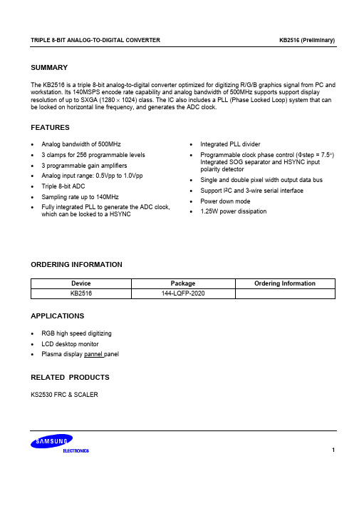
Parameter SOG sync detect level 1 SOG sync detect level 2 Reference top voltage Reference bottom voltage DC integral non-linearity DC differential non-linearity Signal to noise & distortion ratio Max. conversion rate Cross talk Digital output rising time Digital output falling time PLL reference clock frequency Maximum clock frequency PLL divider ratio VCO output clock frequency PLL capture time PLL re-capture time Phase shift step PLL jitter
CLAMP
CLAMP Gain Control Control
CKA (from PLL)
Output Mode
SDA SCL SEN I2C_3W
Gain Control
PLL HSYNC OUT VSYNC OUT CKA CKA CKB
I2C and 3-wire PLL Control
CLAMP Control
KB2516 (Preliminary)
ELECTRICAL CHARACERISTICS
Symbol Power supply VDDC_P VDDC_A VDDA_A VDDD_A VDD_A VDDR VDD_P VDD_S IDDC_P IDDC_A IDDA_A IDDD_A IDD_A IDDR IDD_P IDD_S Ptot Pre-amp f-3dB VIN Vbs AVmax ∆AcG ∆Af1 ∆Af2 tr tf Vbrt1 Vbrt2 Vbrt3 Amplifier bandwidth RGB input voltage range Input bias voltage Voltage gain max Coarse gain diff. between ch. Fine gain diff. 1 between ch. Fine gain diff. 2 between ch. Pre-amp rising time Pre-amp falling time Brightness voltage (1) Brightness voltage (2) Brightness voltage (3) for R, G, B channels for R, G, B channels for R, G, B channels for R, G, B channels for R, G, B channels for R, G, B channels for R, G, B channels for R, G, B channels for R, G, B channels for R, G, B channels 0.5 1.7 1.6 -1.0 -1.0 -1.0 500 0.7 1.9 2.3 0.0 0.0 0.0 1 1 1.5 2.3 3.0 1.0 2.1 2.9 1.0 1.0 1.0 MHz Vpp V dB dB dB dB nS nS V V V Pre-amp analog supply voltage for R, G, B channels ADC analog supply voltage ADC analog supply voltage ADC digital supply voltage ADC digital supply voltage Output driver supply voltage PLL supply voltage Interface logic supply voltage Pre-amp analog supply current ADC analog supply current ADC analog supply current ADC digital supply current ADC digital supply current Output driver supply current PLL supply current Interface logic supply current Total power consumption Fclk = 180MHz, ramp input 5V supply 3.3V supply 5V supply 3.3V supply Fclk = 140MHz, ramp input Fclk = 100MHz 1.25 76 for R, G, B channels for R, G, B channels for R, G, B channels for R, G, B channels for R, G, B channels 4.75 4.75 3.0 4.75 3.0 3.0 3.0 3.0 55 5.0 5.0 3.3 5.0 3.3 3.3 3.3 3.3 65 66 33 10 20 5.25 5.25 3.6 5.25 3.6 3.6 3.6 3.6 75 V V V V V V V V mA mA mA mA mA mA mA mA W Parameter Conditions Min. Typ. Max. Unit
Vigor2920 系

Vigor2920 系列雙WAN安全防護路由器快速安裝手冊版本: 1.0韌體版本: V3.3.3.1日期: 19/07/2010因手冊更新無法及時通知用戶,請隨時連上居易網站,取得最新的手冊內容。
版權資訊版權聲明© 2010版權所有,翻印必究。
此出版物所包含資訊受版權保護。
未經版權所有人書面許可,不得對其進行拷貝、傳播、轉錄、摘錄、儲存到檢索系統或轉譯成其他語言。
交貨以及其他詳細資料的範圍若有變化,恕不預先通知。
商標本手冊內容使用以下商標:z Microsoft為微軟公司註冊商標z Windows視窗系列,包括Windows 95, 98, Me, NT, 2000, XP 以及其Explorer均屬微軟公司商標z Apple以及Mac OS均屬蘋果電腦公司的註冊商標z其他產品則為各自生產廠商之註冊商標安全說明和保障安全說明z在設置前請先閱讀安裝說明。
z由於路由器是複雜的電子產品,請勿自行拆除或是維修本產品。
z請勿自行打開或修復路由器。
z請勿把路由器置於潮濕的環境中,例如浴室。
z請將本產品放置在足以遮風避雨之處,適合溫度在攝氏5度到40度之間。
z請勿將本產品暴露在陽光或是其他熱源下,否則外殼以及零件可能遭到破壞。
z請勿將LAN網線置於戶外,以防電擊危險。
z請將本產品放置在小孩無法觸及之處。
z若您想棄置本產品時,請遵守當地的保護環境的法律法規。
保固自使用者購買日起二年內為保固期限,請將您的購買收據保存二年,因為它可以證明您的購買日期。
當本產品發生故障乃導因於製作及(或)零件上的錯誤,只要使用者在保固期間內出示購買證明,居易科技將採取可使產品恢復正常之修理或更換有瑕疵的產品(或零件),且不收取任何費用。
居易科技可自行決定使用全新的或是同等價值且功能相當的再製產品。
下列狀況不在本產品的保固範圍內:(1)若產品遭修改、錯誤(不當)使用、不可抗力之外力損害,或不正常的使用,而發生的故障;(2) 隨附軟體或是其他供應商提供的授權軟體;(3) 未嚴重影響產品堪用性的瑕疵。
JK2516C 系列精密电阻测试仪使用说明书

JK2516C系列精密电阻测试仪使用说明书USER MANUAL简体中文版Simplified Chinese2017第二版Rev1.00注意:本说明书所描述的可能并非仪器所有内容,所含资料在印制之前已经过校正,但因公司不断改善产品,所以保留未来修改产品规格、特性、内部结构、外观、附件、包装物以及保养维修程序的权利,因此内容可能会有变动,不必事前通知。
由此引起目录安全说明 (3)安全指南 (4)有限担保和责任范围 (5)第1章仪器检查与准备 (6)1.1装箱清单 (6)1.2电源要求 (6)1.3保险丝 (7)1.4操作环境 (7)1.5测试夹具的使用 (7)1.6清洗 (7)第2章产品概述 (8)2.1引言 (8)2.2型号说明 (8)2.3主要规格 (9)2.4主要功能 (9)第3章产品介绍 (10)3.1认识前面板 (10)3.1.1键区 (11)3.2后面板概述 (12)3.3TFT——LCD介绍(主显示区域定义) (13)第4章仪器操作及说明 (15)4.1上电启动(开机) (15)4.2参数设置与数值输入方法 (15)4.3开始测试 (16)4.3.1测试端的连接 (16)4.3.2清零 (16)4.4测量界面(主界面) (17)4.5档计数界面 (19)4.6文件界面 (20)4.7文件系统说明 (21)4.8系统设置界面 (22)第5章分选比较器 (23)5.1分选模式 (23)5.2讯响 (23)5.3分选流程 (23)第6章远程控制 (25)6.1RS232接口说明 (25)6.2USB接口说明 (25)6.3仪器通讯协议 (27)6.3.1下位机(仪器)通讯协议 (27)6.3.2上位机(计算机)通讯协议 (27)6.4HANDLER接口说明 (29)6.4.1管脚说明: (29)6.4.2输入输出端电路原理图: (30)附录A:电阻测试基本准确度 (31)安全说明本章节包含仪器操作和存储时必须遵照的重要安全说明。
Dell UltraSharp UP2516D UP2716D显示器用户指南说明书

Dell UltraSharp UP2516D/UP2716D 用户指南规格型号: UP2516D/UP2716D 注:“注”表示可以帮助您更好使用显示器的重要信息。
注意:“注意”表示如果不按照说明进行操作,可能造成硬件损坏或数据丢失。
警告:“警告”表示可能会造成财产损失、人身伤害或死亡。
版权所有© 2015-2019 Dell Inc. 保留所有权利。
本产品受美国和国际版权和知识产权法律的保护。
Dell™和Dell 徽标是Dell Inc.在美国和/或其他司法管辖区域的商标。
本文提到的所有其他标记和名称分别是其相应公司的商标。
2019 – 10 Rev. A05目录关于您的显示器 . . . . . . . . . . . . . . . . . . . . . . . . . . . . . . . . . . . . . . . . . . 5物品清单 . . . . . . . . . . . . . . . . . . . . . . . . . . . . . . . . . . . . . . 5产品特性 . . . . . . . . . . . . . . . . . . . . . . . . . . . . . . . . . . . . . . 6识别部件和控制 . . . . . . . . . . . . . . . . . . . . . . . . . . . . . . . . . . 7显示器规格 (10)即插即用 . . . . . . . . . . . . . . . . . . . . . . . . . . . . . . . . . . . . . 22液晶显示器质量和像素政策 . . . . . . . . . . . . . . . . . . . . . . . . . . 22设置显示器 . . . . . . . . . . . . . . . . . . . . . . . . . . . . . . . . . . . . . . . . . . . . . 23安装底座 . . . . . . . . . . . . . . . . . . . . . . . . . . . . . . . . . . . . . 23使用倾斜、旋转和垂直展开功能 (26)调节系统的旋转显示设置 (27)连接显示器 (27)整理线缆. . . . . . . . . . . . . . . . . . . . . . . . . . . . . . . . . . . . . 30卸下底座 . . . . . . . . . . . . . . . . . . . . . . . . . . . . . . . . . . . . . 31壁挂(可选) . . . . . . . . . . . . . . . . . . . . . . . . . . . . . . . . . . 32操作显示器 . . . . . . . . . . . . . . . . . . . . . . . . . . . . . . . . . . . . . . . . . . . . . 33打开显示器电源 . . . . . . . . . . . . . . . . . . . . . . . . . . . . . . . . . 33使用前面板控制 . . . . . . . . . . . . . . . . . . . . . . . . . . . . . . . . . 33使用屏幕显示(OSD)菜单 . . . . . . . . . . . . . . . . . . . . . . . . . . 36故障排除 . . . . . . . . . . . . . . . . . . . . . . . . . . . . . . . . . . . . . . . . . . . . . . . 49自检. . . . . . . . . . . . . . . . . . . . . . . . . . . . . . . . . . . . . . . . 49目录 | 3内置诊断 . . . . . . . . . . . . . . . . . . . . . . . . . . . . . . . . . . . . . 50常见问题 . . . . . . . . . . . . . . . . . . . . . . . . . . . . . . . . . . . . . 51产品特定问题 . . . . . . . . . . . . . . . . . . . . . . . . . . . . . . . . . . 52 Mobile High-Definition Link (MHL)特定问题 (53)附录 . . . . . . . . . . . . . . . . . . . . . . . . . . . . . . . . . . . . . . . . . . . . . . . . . . . 54安全说明 . . . . . . . . . . . . . . . . . . . . . . . . . . . . . . . . . . . . . 54 FCC 声明(仅限美国)和其他管制信息 . . . . . . . . . . . . . . . . . . . 54联系 Dell . . . . . . . . . . . . . . . . . . . . . . . . . . . . . . . . . . . . . 54设置显示器 . . . . . . . . . . . . . . . . . . . . . . . . . . . . . . . . . . . 55维护指南 . . . . . . . . . . . . . . . . . . . . . . . . . . . . . . . . . . . . . 56中国能源效率标识: . . . . . . . . . . . . . . . . . . . . . . . . . . . . . . . 564 | 目录关于您的显示器 | 5关于您的显示器物品清单此显示器在出厂时包括如下所示的物品。
ICN2516_CH中文规格书_V2
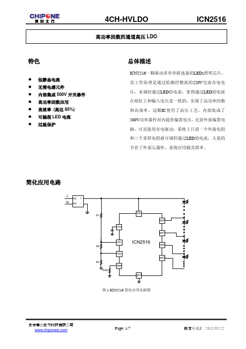
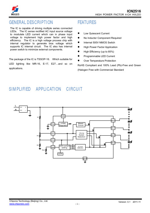
特色● 低静态电流 ● 无需电感元件● 内部集成500V 开关器件 ● 高功率因数应用 ● 高效率 (高达85%) ● 可编程LED 电流 ●过温保护总体描述ICN2516一颗驱动多串串联连接的LEDs 照明芯片,其工作原理是通过检测经整流的220V 交流市电电压,来调控通过LED 的电流,使得通过LED 的电流在相位上和输入电压是一致的,实现了高功率因数和高效率。
这颗IC 使用了高压工艺,内部集成了500V 功率器件对内提供偏置电压,无需外部偏置电路,可直接用市电驱动,系统上只需一个外接电阻和三个采样电阻就可调控通过LED 的电流,大量的节省了外部元器件,系统应用极其简单。
简化应用电路图1 ICN2516简化应用电路图注:* 功耗值是基于结温和环境温差100°C计算出来的;* 超出绝对最大允许范围可能会对芯片造成永久性损坏。
电气参数工作原理ICN2516的具体工作原理如下图2所示,经整流后的220V AC 市电直接加到IC 上,利用如图1所示的采样电阻R1、R2和R3对交流市电进行采样。
采样到的电压经过IC 内部电路判断处理,打开对应的开关SW0~SW3如图2。
通过开关SW0~SW3的电流和图2所示的电流I0~I3各自分别对应,并且I0到I3电流呈台阶上升,在相位上和220V AC 市电一致,实现了高达98%的功率因数。
此外,该芯片还可通过调整Rset 电阻来调节负载LED 的电流,也就是说LED 灯的输出功率也可通过Rset 电阻来调节。
负载LED 电流由如下公式计算:()()()Iset Iset Iset I0I1V /Rset *1500I2V /Rset *2000I3V /Rset *2500,,通过开关SW0~SW3的电流I SW 和开关电压V SW 的关系如下图3所示,只需在SW 端加较小的电压就可以实现恒定的输出电流,如32mA@3.5V 。
这样就可以尽可能的增加负载LED 数量,减小IC 本身的功耗,提高转换效率(高达85%)。
电动不锈钢法兰连接闸阀-上海博球防腐阀门有限

电动不锈钢法兰连接闸阀说明:高中压法兰连接的闸阀适用于公称压力PN1.6~16.0MPa,工作温度≤-29℃~550℃的石油、化工、水力、火力电站各种系统的管路上,切断或接通管路介质。
适用介质为:水、油品、蒸气、及酸、碱、氨、尿素、含硫天然气等。
电动不锈钢法兰连接闸阀结构特点1、选材考究,符合国内外相关标准,材料的全面质量高。
2、符合国内外先进标准的要求,密封可靠、性能优良、造型美观。
3、密封副配对先进合理,闸板和阀座的密封面采用不同硬度的司太立(Stellite)钴基硬质合金堆焊而成,密封可靠、硬度高、耐磨、耐高温、耐腐蚀、抗擦伤性能好、寿命长。
4、阀杆经调质及表面氮化处理,有良好的抗腐蚀性、抗擦伤性和耐磨性。
5、采用楔式弹性闸板结构,中大口径设置推力轴承,磨擦力小,并配有撞击手动,启闭轻松自如。
6、可采用各种配管法兰标准及法兰密封面形式,满足各种工程需要及用户要求。
电动不锈钢法兰连接闸阀产品说明Z941W 型PN16~PN200 不锈钢楔式闸阀:电动、法兰连接、明杆楔式刚性单闸板,阀座密封面材料为不锈钢,公称压力PN16~PN200,阀体材料为不锈钢的闸阀。
电动不锈钢法兰连接闸阀产品性能参数Z941W 型PN16~PN200 不锈钢楔式闸阀主要性能参数型号PN 工作压力/MPa适用温度/℃适用介质Z941W-16 P~200P 16~2004.0~10.0 ≤200硝酸类介质Z941W-16R~200R醋酸类介质电动不锈钢法兰连接闸阀产品零部件材料Z941W 型PN16~PN200 不锈钢楔式闸阀零部件材料型号材料阀体、阀盖闸板阀杆填料Z94 1W-16P ~200 P 铬镍不锈钢铬镍不锈钢铬镍不锈钢聚四氟乙烯Z94 1W-16R 铬镍钼铬镍钼不锈钢铬镍钼~200 R 不锈钢不锈钢不锈钢电动闸阀产品外形及结构尺寸Z941W-16P、Z941W-16R 型不锈钢楔式闸阀主要外形及结构尺寸(mm)D N L DD1D2b fz×ΦdH重量/Kg5 0 251612511634×Φ18653596 5 26518145121834×Φ18665628 0 2819516135238×Φ18725741 0 0 321518155238×Φ18787921 2 5 325245211852238×Φ18921521 5 0 352824212438×Φ239551612 0 0 433529526526312×Φ231152192 5 0 4545355323312×Φ2513433763 0 0 5546413753412×Φ251516484355443 4 1616955 0 527354 ×Φ256784 0 0 65852548536416×Φ3018499774 5 0 65645855454420×Φ30193710335 0 0 775656844420×Φ34223410876 0 0 8847771848520×Φ41243213577 0 0 991847885524×Φ41248914818 0 0 1129589852524×Φ4126431845Z941W-25P、Z941W-25R 型不锈钢楔式闸阀主要外形及结构尺寸(mm)D N L DD1D2b fz×ΦdH重量/Kg5 0 25161251234×Φ18653646 5 26518145122238×Φ2366565821112 3 8×7790 80 956352 Φ18251 0 0 32319162438×Φ23787981 2 5 32527221882838×Φ25921542 0 0 43625218338×Φ259551682 5 0 454253733236312×Φ3013433903 0 0 548543394416×Φ3015165053 5 0 55554944844416×Φ3416787364 0 0 661555548416×Φ34184910274 5 0 656665555420×Φ34193711395 0 0 773666152420×Φ41223412286 0 0 8847771856520×Φ41243150227 0 0 99558758156524×Φ48248916178 0 0 117999364524×Φ4826431923Z941W-40P、Z941W-40R 型不锈钢楔式闸阀主要外形及结构尺寸(mm)D N L DD1D2D6b ff1z×ΦdH重量/Kg5 0 251612518823 44×Φ18665586 5 28181451211223 48×Φ1868688 0 3119516135121223 48×Φ18752801 0 0 35231916152434.58×Φ238461081 2 5 427221881762834.58×Φ259231511 5 0 4532521824334.58×Φ251872582 0 0 5537532282263834.512×Φ3012433662 565443834314234.12×Φ144720 0 5 5 5 3 5 34 293 0 0 755145483644634.516×Φ341686733 5 0 855751465422524 516×Φ3417388044 0 0 95655585535474584 516×Φ41189710814 5 0 1568615652464 520×Φ4121412595 0 0 11575567612576624 520×Φ482411348Z941W-64P、Z941W-64R 型不锈钢楔式闸阀主要外形及结构尺寸(mm)D N L DD1D2D6b ff1z×ΦdH重量/Kg5 0 251751351588263 44×Φ23667686 5 282161311283 48×Φ23685728 0 3121171412133 48×Φ23748881 0 0 35252168153234.58×Φ258451171 2 5 429524221763634.58×Φ39351581 5 0 45342824243834.58×Φ34193142 0 0 55453453264434.512×Φ3412534322 5 0 654743523134834.512×Φ4114495953 0 0 7553464123645444.516×Φ4118677213 5 0 8559552547542264 516×Φ4119319634 0 0 9567585525474664 516×Φ4821711295 0 0 1158756457674 520×Φ5424591493Z941W-100P、Z941W-100R 型不锈钢楔式闸阀主要外形及结构尺寸(mm)D N L DD1D2D6b ff1z×ΦdH重量/Kg5 0 2519514511288283 44×Φ25781786 5 28221713811323 48×Φ2583968 0 312318148121343 48×Φ258651261 0 0 352652117515383 48×Φ311791341 2 5 43125211764234.58×Φ341192001 5 0 45352925244634.512×Φ341213522 0 0 554336312265434.512×Φ4116114842 5 0 65543382313634.512×Φ411936083 0 0 755855442364744.516×Φ482547573 5 0 8565556498422764 516×Φ5421329944 0 0 957156255847484 516×Φ5423211269Z941W-160P 型不锈钢楔式闸阀主要外形及结构尺寸(mm)D N L DD1D2D6bz×ΦdH重量/Kg5 0 321516513295368×Φ2572506 5 342451915211448×Φ3752508 0 39262516813468×Φ38152501 0 0 45324216488×Φ3486-1 2 5 5253552852381968×Φ4197-1 5 0 63931827256612×Φ411224-2 0 0 754843452757812×Φ48149-Z941W-200P 型不锈钢楔式闸阀主要外形及结构尺寸(mm)D N L DD1D2D6bz×ΦdH重量/Kg5 0 3521161289548×Φ27712-6 5 41262316511488×Φ3765-84221158×8-0 70 93964 Φ3451 0 0 553629224519668×Φ4198-1 2 5 6538531827257612×Φ4118-1 5 0 75443635248212×Φ48114-。
2.5U工业便携机
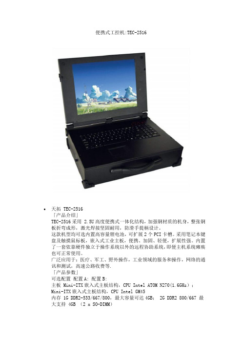
便携式工控机:TEC-2516天拓 TEC-2516「产品介绍」TEC-2516采用 2.5U高度便携式一体化结构,加强钢材质的机身,整张钢板折弯成形,激光焊接坚固耐用,防滑手提柄设计。
这款机型均可选内置高容量锂电池,可扩展2个PCI卡槽。
采用笔记本键盘及触摸鼠标板,嵌入式工业主板,便携、加固、轻便,扩展性强。
内置了一套依靠硬件独立于操作系统以外的远程协助系统,即便主机系统瘫痪也可正常使用。
广泛应用于:医疗、军工、野外操作,工业领域的服务和操作,网络的通讯和测试,高速公路收费等.「产品参数」可选配置配置A: 配置B:主板 Mini-ITX嵌入式主板结构,CPU Intel ATOM N270(1.6GHz);Mini-ITX嵌入式主板结构,CPU Intel GM45内存 1G DDR2-533/667/800,最大容量可达4GB; 2G DDR2 800/667 最大支持 4GB (2 x SO-DIMM)CPU 板载N270 1.6 GHZ 酷睿双核T7300 2.0 GHz硬盘内置320G硬盘内置500G硬盘光驱超薄COMBO(可选DVD-RW)接口预留4个USB接口、1个串口、1个并口、100M网络接口、音频接口、VGA接口;预留4个USB接口、1个串口、2个1000M网络接口、音频接口、1个VGA接口、2个HDMI;显示屏 15"TFT LCD;分辨率1024×768;亮度 250cd/㎡键盘鼠标标配99键笔记本键盘,触摸式鼠标;电源 9V-30V直流输入,可选配锂电池供电。
物理参数扩展升级可扩展2个PCI设备机箱结构金属结构机箱,(或铝镁合金结构机箱)减震设计机箱四角共有6减震橡胶垫独创的硬盘减震技术,使得数据更加安全工作温度0℃~50℃储存温度 -20℃~60℃储存湿度 5%~95%(不凝露)抗冲击 15G@11ms抗振动 4.2G(50-500Hz)尺寸(mm) 430x350x115重量≤9.8kg机箱颜色黑色,银灰(可选其它颜色)机箱结构可扩展1个PCI设备铝合金结构机箱,使整机更加轻便机箱四角共有4减震橡胶垫独创的硬盘减震技术,使得数据更加安全颜色:黑色,银灰(可选其它颜色)。
W942508AH-7G资料
8M × 4 BANKS × 8 BIT DDR SDRAMPublication Release Date: March 12, 2002Table of Contents-1. GENERAL DESCRIPTION..................................................................................................................3 2. FEATURES..........................................................................................................................................3 3. KEY PARAMETERS............................................................................................................................3 4. PIN CONFIGURATION........................................................................................................................4 5. PIN DESCRIPTION .............................................................................................................................5 6. BLOCK DIAGRAM...............................................................................................................................6 7. ABSOLUTE MAXIMUM RATINGS......................................................................................................7 8. RECOMMENDED DC OPERATING CONDITIONS............................................................................7 9. CAPACITANCE ...................................................................................................................................8 10. LEAKAGE AND OUTPUT BUFFER CHARACTERISTICS...............................................................8 11. DC CHARACTERISTICS...................................................................................................................9 12. AC CHARACTERISTICS AND OPERATING CONDITION.............................................................10 13. AC TEST CONDITIONS..................................................................................................................11 14. OPERATION MODE (13)Simplified Truth Tabl (13)Function Truth Table .............................................................................................................................14 Function Truth Table for CKE. (17)15. SIMPLIFIED STATE DIAGRAM ......................................................................................................18 16. FUNCTIONAL DESCRIPTION.. (19)Power Up Sequence..............................................................................................................................19 Command Function. (19)Read Operation.....................................................................................................................................22 Write Operation .....................................................................................................................................22 Precharge..............................................................................................................................................22 Burst Termination..................................................................................................................................23 Refresh Operation.................................................................................................................................23 Power Down Mode................................................................................................................................23 Mode Register Operation . (23)17. TIMING WAVEFORMS (27)Command Input Timing (27)Timing of the CLK Signals.....................................................................................................................27 Read Timing (Burst Length = 4) (28)Write Timing (Burst Length = 4) (29)DM, DATA MASK (W942508AH/W942504AH) (30)DM, DATA MASK (W942516AH) (30)Mode Register Set (MRS) Timing (31)Extend Mode Register Set (EMRS) Timing (32)Auto Precharge Timing (Read cycle, CL = 2) (33)Auto Precharge Timing (Write Cycle) (35)Read Interrupted by Read (CL = 2, BL = 2, 4, 8) (36)Burst Read Stop (BL = 8) (36)Read Interrupted by Write & BST (BL = 8) (37)Read Interrupted by Precharge (BL = 8) (37)Write Interrupted by Write (BL = 2, 4, 8) (38)Write Interrupted by Read (CL = 2, BL = 8) (38)Write Interrupted by Read (CL = 2.5, BL = 4) (39)Write Interrupted by Precharge (BL = 8) (39)2 Bank Interleave Read Operation (CL = 2, BL = 2) (40)2 Bank Interleave Read Operation (CL = 2, BL = 4) (40)4 Bank Interleave Read Operation (CL = 2, BL = 2) (41)4 Bank Interleave Read Operation (CL = 2, BL = 4) (41)Auto Refresh Cycle (42)Active Power Down Mode Entry and Exit Timing (42)Precharged Power Down Mode Entry and Exit Timing (42)Self Refresh Entry and Exit Timing (43)18. PACKAGE DIMENSION (44)TSOP 66l – 400 mil (44)19. VERSION HISTORY (45)Publication Release Date: March 12, 20021. GENERAL DESCRIPTIONW942508AH is a CMOS Double Data Rate synchronous dynamic random access memory (DDR SDRAM), organized as 8,388,608 words × 4 banks × 8 bits. Using pipelined architecture and 0.175 µm process technology, W942508AH delivers a data bandwidth of up to 286M words per second (-7). To fully comply with the personal computer industrial standard, W942508AH is sorted into three speed grades: -7, -75 The -7 is compliant to the 143 MHz/CL2.5 or DDR266/CL2 specification, the -75 is compliant to the DDR266/CL2.5 specification.All Inputs reference to the positive edge of CLK (except for DQ, DM, and CKE). The timing reference point for the differential clock is when the CLK and CLK signals cross during a transition. And Write and Read data are synschronized with the both edges of DQS (Data Strobe).By having a programmable Mode Register, the system can change burst length, latency cycle, interleave or sequential burst to maximize its performance. W942508AH is ideal for main memory in high performance applications.2. FEATURES• 2.5V ±0.2V Power Supply• Up to 143 MHz Clock Frequency• Double Data Rate architecture; two data transfers per clock cycle• Differential clock inputs (CLK and CLK )• DQS is edge-aligned with data for Read; center-aligned with data for Write • CAS Latency: 2 and 2.5 • Burst Length: 2, 4 and 8• Auto Refresh and Self Refresh• Precharged Power Down and Active Power Down • Write Data Mask • Write Latency = 1• 8K Refresh cycles / 64 mS • Interface: SSTL-2• Packaged in TSOP II 66-pin, 400 x 875 mil, 0.65mm pin pitch3. KEY PARAMETESYMBOLDESCRIPTIONMIN./MAX.-7-75t CK Clock Cycle Time CL = 2 Min. 7.5 nS 8 nSCL = 2.5Min. 7 nS 7.5 nS t RAS Active to Precharge Command Period Min. 45 nS 45 nS t RC Active to Ref/Active Command Period Min. 65 nS 65 nS I DD1 Operation Current (Single bank) Max. 110 mA 110 mA I DD4 Burst Operation Current Max. 165 mA 155 mA I DD6Self Refresh CurrentMax.3 mA3 mA4. PIN CONFIGURATIONPublication Release Date: March 12, 20025. PIN DESCRIPTION6. BLOCK DIAGRAMCKEA10Publication Release Date: March 12, 20027. ABSOLUTE MAXIMUM RATINGSPARAMETERSYMBOL RATING UNIT Input/Output Voltage V IN , V OUT -0.3 ~ V DD Q +0.3VPower Supply Voltage V DD , V DDQ-0.3 ~ 3.6 VOperating Temperature T OPR 0 ~ 70 °C Storage Temperature T STG -55 ~ 150 °CSoldering Temperature (10s) T SOLDER260 °CPower DissipationP D 1 WShort Circuit Output CurrentI OUT50mA8. RECOMMENDED DC OPERATING CONDITIONS(T A = 0 to 70°C)Notes: Undershoot Limit: V IL (min) = -0.9V with a pulse width < 5 nSOvershoot Limit: V IH (max) = V DD Q +0.9V with a pulse width < 5 nS V IH (DC) and V IL (DC) are levels to maintain the current logic state. V IH (AC) and V IL (AC) are levels to change to the new logic state.9. CAPACITANCE(V DD = V DD Q = 2.5V ±0.2V, f = 1 MHz, T A = 25°C, V OUT (DC) = V DD Q/2, V OUT (Peak to Peak) = 0.2V)SYMBOL PARAMETERMIN. MAX. DELTA(MAX.) UNITC IN Input Capacitance (except for CLK pins) 2.0 3.0 0.5 pF C CLK Input Capacitance (CLK pins) 2.0 3.0 0.25 pF C I/O DQ, DQS, DM Capacitance 4.0 5.0 0.5 pF C NC1 NC1 Pin Capacitance - 1.5 - pF C NC2NC2 Pin Capacitance4.05.0-pFNotes: These parameters are periodically sampled and not 100% tested.The NC2 pins have additional capacitance for adjustment of the adjacent pin capacitance. The NC2 pins have Power and Ground clamp.10. LEAKAGE AND OUTPUT BUFFER CHARACTERISTICSSYMBOL PARAMETERMIN. MAX. UNITS NOTES I I(L) Input Leakage Current(0V < V IN < V DD Q, All other pins not under test = 0V) -2 2 µA I O(L) Output Leakage Current(Output disabled, 0V < V OUT < V DD Q) -5 5 µA V OH Output High Voltage(under AC test load condition) V TT +0.76- V V OL Output Low Voltage(under AC test load condition)- V TT -0.76 V I OH (DC)Output Minimum Source DC Current-15.2 - mA 4, 6 I OL (DC) Output Minimum Sink DC Current Full Strength15.2 - mA 4, 6 I OH (DC) Output Minimum Source DC Current -10.4 - mA 5 I OL (DC) Output Minimum Sink DC CurrentHalf Strength10.4-mA5Publication Release Date: March 12, 200211. DC CHARACTERISTICSCK CKDQSRANDOM READ CURRENT TimingtRCDt RC12. AC CHARACTERISTICS AND OPERATING CONDITION(Notes: 10, 12)Publication Release Date: March 12, 200213. AC TEST CONDITIONSV SWING (MAX)V DD QV SS(9) These parameters depend on the output loading. Specified values are obtained with the output open.(10) Transition times are measured between V IH min(AC) and V IL max(AC).Transition (rise and fall) of input signals have afixed slope.(11) IF the result of nominal calculation with regard to t CK contains more than one decimal place, the result is rounded up tothe nearest decimal place. (i.e., t DQSS = 0.75 × t CK , t CK = 7.5 nS, 0.75 × 7.5 Ns = 5.625 nS is rounded up to 5.6 nS.)(12) V X is the differential clock cross point voltage where input timing measurement is referenced.(13) V ID is magnitude of the difference between CLK input level and CLK input level.(14) V ISO means {V ICK (CLK)+V ICK (CLK )}/2.(15) Refer to the figure below.CLKV V XXV V XV (16) t AC and t DQSCK depend on the clock jitter. These timing are measured at stable clock.Publication Release Date: March 12, 200214. OPERATION MODEThe following table shows the operation commands.Simplified Truth TablNotes :1. V = Valid X = Don’t Care L = Low level H = High level2. CKE n signal is input level when commands are issued.CKE n-1 signal is input level one clock cycle before the commands are issued. 3. These are state designated by the BS0, BS1 signals. 4. LDM, UDM (W942516AH)5. Power Down Mode can not entry in the burst cycle.Function Truth Table(Note 1)Publication Release Date: March 12, 2002Function Truth Table, continuedFunction Truth Table, continuedNotes :1. All entries assume that CKE was active (High level) during the preceding clock cycle and the current clock cycle.2. Illegal if any bank is not idle.3. Illegal to bank in specified states; Function may be legal in the bank indicated by Bank Address (BS), depending on thestate of that bank.4. Illegal if t RCD is not satisfied.5. Illegal if t RAS is not satisfied.6. Must satisfy burst interrupt condition.7. Must avoid bus contention, bus turn around, and/or satisfy write recovery requirements. 8. Must mask preceding data which don’t satisfy t WRRemark: H = High level, L = Low level, X = High or Low level (Don’t care), V = Valid dataPublication Release Date: March 12, 2002Function Truth Table for CKENotes :1. Self refresh can enter only from the all banks idle state.2. Power down can enter only from bank idle or row active state.Remark: H = High level, L = Low level, X = High or Low level (Don’t care), V = Valid data15. SIMPLIFIED STATE DIAGRAMPublication Release Date: March 12, 200216. FUNCTIONAL DESCRIPTIONPower Up Sequence(1) Apply power and attempt to CKE at a low state (≤0.2V), all other inputs may be undefined1) Apply V DD before or at the same time as V DD Q.2) Apply V DD Q before or at the same time as V TT and V REF . (2) Start Clock and maintain stable condition for 200µS (min). (3) After stable power and clock, apply NOP and take CKE high.(4) Issue EMRS (Extended Mode Register Set) to enable DLL and establish Output Driver Type. (5) Issue MRS (Mode Register Set) to reset DLL and set device to idle with bit A8.(an additional 200 cycles(min) of clock are required for DLL Lock) (6) Issue precharge command for all banks of the device. (7) Issue two or more Auto Refresh commands. (8) Issue MRS-Initialize device operation.(If device operation mode is set at sequence 5, sequence 8 can be skipped.)Command Function1. Bank Activate Command(RAS = "L", CAS = "H", WE = "H", BS0, BS1 = Bank, A0 to A12 = Row Address)The Bank Activate command activates the bank designated by the BS (Bank address) signal. Row addresses are latched on A0 to A12 when this command is issued and the cell data is read out of the sense amplifiers. The maximum time that each bank can be held in the active state is specified as t RAS (max). After this command is issued, Read or Write operation can be executed.2. Bank Precharge Command(RAS = "L", CAS = "H", WE = "L", BS0, BS1 = Bank, A10 = "L", A0 to A9, A11, A12 = Don’t care)The Bank Precharge command percharges the bank designated by BS. The precharged bank is switched from the active state to the idle state.3. Precharge All Command(RAS = "L", CAS = "H", WE = "L", BS0, BS1 = Don’t care , A10 = "H", A0 to A9, A11, A12 = Don’t care)The Precharge All command precharges all banks simultaneously. Then all banks are switched to the idle state.4. Write Command(RAS = "H", CAS = "L", WE = "L", BS0, BS1 = Bank, A10 = "L", A0 to A9, A11 = Column Address)The write command performs a Write operation to the bank designated by BS. The write data are latched at both edges of DQS. The length of the write data (Burst Length) and column access sequence (Addressing Mode) must be in the Mode Register at power-up prior to the Write operation.5. Write with Auto Precharge Command(RAS="H", CAS= "L", WE= "L", BS0, BS1 = Bank, A10= "H", A0 to A9, A11 = Column Address) The Write with Auto Precharge command performs the Precharge operation automatically after the Write operation. This command must not be interrupted by any other commands.6. Read Command(RAS="H", CAS= "L", WE= "H", BS0, BS1 = Bank, A10 = "L", A0 to A9, A11 = Column Address) The Read command performs a Read operation to the bank designated by BS. The read data are synchronized with both edges of DQS. The length of read data (Burst Length), Addressing Mode and CAS Latency (access time from CAS command in a clock cycle) must be programmed in the Mode Register at power-up prior to the Read operation.7. Read with Auto Precharge Command(RAS = "H", CAS = "L", WE = "H", BS0, BS1 = Bank, A10 = "H", A0 to A9, A11 = Column Address)The Read with Auto precharge command automatically performs the Precharge operation after the Read operation.1) READA≥t RAS (min) - (BL/2) x t CKInternal precharge operation begins after BL/2 cycle from Read with Auto Precharge command. 2) t RCD(min) ≤ READA < t RAS(min) - (BL/2) x t CKData can be read with shortest latency, but the internal Precharge operation does not begin until after t RAS (min) has completed.This command must not be interrupted by any other command.8. Mode Register Set Command(RAS = "L", CAS = "L", WE = "L", BS0 = "L", BS1 = "L", A0 to A12 = Register Data)The Mode Register Set command programs the values of CAS latency, Addressing Mode, Burst Length and DLL reset in the Mode Register. The default values in the Mode Register after power-up are undefined, therefore this command must be issued during the power-up sequence. Also, this command can be issued while all banks are in the idle state. Refer to the table for specific codes.9. Extended Mode Register Set Command(RAS = "L", CAS = "L", WE = "L", BS0 = "H", BS1 = "L", A0 to A12 = Register data)The Extended Mode Register Set command can be implemented as needed for function extensions to the standard (SDR-SDRAM). Currently the only available mode in EMRS is DLLPublication Release Date: March 12, 2002enable/disable, decoded by A0. The default value of the extended mode register is not defined; therefore this command must be issued during the power-up sequence for enabling DLL. Refer to the table for specific codes.10. No-Operation Command(RAS = "H", CAS = "H", WE = "H")The No-Operation command simply performs no operation (same command as Device Deselect).11. Burst Read Stop Command(RAS = "H", CAS = "H", WE = "L")The Burst stop command is used to stop the burst operation. This command is only valid during a Burst Read operation.12. Device Deselect Command(CS ="H")The Device Deselect command disables the command decoder so that the RAS ,CAS ,WE and Address inputs are ignored. This command is similar to the No-Operation command.13. Auto Refresh Command(RAS = "L", CAS = "L", WE = "H", CKE = "L", BS0, BS1, A0 to A12 = Don’t care)The Auto Refresh command is used to refresh the row address provided by the internal refresh counter. The Refresh operation must be performed 8192 times within 64ms. The next command can be issued after t REF from the end of the Auto Refresh command. When the Auto Refresh command is used, all banks must be in the idle state.14. Self Refresh Entry Command(RAS = "L", CAS = "L", WE = "H", CKE = "L", BS0, BS1, A0 to A12 = don’t care)The Self Refresh Entry command is used to enter Self Refresh mode. While the device is in Self Refresh mode, all input and output buffer (except the CKE buffer) are disabled and the Refresh operation is automatically performed. Self Refresh mode is exited by taking CKE "high" (the Self Refresh Exit command). During self refresh, DLLl is disable.15. Self Refresh Exit Command(CKE = "H", CS = "H" or CKE = "H", RAS = "H", CAS = "H")This command is used to exit from Self Refresh mode. Any subsequent commands can be issued after t XSNR (t XSRD for Read Command) from the end of this command.16. Data Write Enable /Disable Command(DM = "L/H" or LDM, UDM = "L/H")During a Write cycle, the DM or LDM, UDM signal functions as Data Mask and can control every word of the input data. The LDM signal controls DQ0 to DQ7 and UDM signal controls DQ8 to DQ15.Read OperationIssuing the Bank Activate command to the idle bank puts it into the active state. When the Read command is issued after t RCD from the Bank Activate command, the data is read out sequentially, synchronized with both edges of DQS (Burst Read operation). The initial read data becomes available after CAS latency from the issuing of the Read command. The CAS latency must be set in the Mode Register at power-up.When the Precharge Operation is performed on a bank during a Burst Read and operation, the Burst operation is terminated.When the Read with Auto Precharge command is issued, the Precharge operation is performed automatically after the Read cycle, then the bank is switched to the idle state. This command cannot be interrupted by any other commands. Refer to the diagrams for Read operation.Write OperationIssuing the Write command after t RCD from the bank activate command. The input data is latched sequentially, synchronizing with both edges(rising &falling) of DQS after the Write command (Burst write operation). The burst length of the Write data (Burst Length) and Addressing Mode must be set in the Mode Register at power-up.When the Precharge operation is performed in a bank during a Burst Write operation, the Burst operation is terminated.When the Write with Auto Precharge command is issued, the Precharge operation is performed automatically after the Write cycle, then the bank is switched to the idle state, The Write with Auto Precharge command cannot be interrupted by any other command for the entire burst data duration. Refer to the diagrams for Write operation.PrechargeThere are two Commands, which perform the precharge operation (Bank Precharge and Precharge All). When the Bank Precharge command is issued to the active bank, the bank is precharged and then switched to the idle state. The Bank Precharge command can precharge one bank independently of the other bank and hold the unprecharged bank in the active state. The maximum time each bank can be held in the active state is specified as t RAS (max). Therefore, each bank must be precharged within t RAS(max) from the bank activate command.The Precharge All command can be used to precharge all banks simultaneously. Even if banks are not in the active state, the Precharge All command can still be issued. In this case, the Precharge operation is performed only for the active bank and the precharge bank is then switched to the idle state.Publication Release Date: March 12, 2002Burst TerminationWhen the Precharge command is used for a bank in a Burst cycle, the Burst operation is terminated. When Burst Read cycle is interrupted by the Precharge command, read operation is disabled after clock cycle of (CAS latency) from the Precharge command. When the Burst Write cycle is interrupted by the Precharge command . the input circuit is reset at the same clock cycle at which the precharge command is issued. In this case, the DM signal must be asserted "high": during t WR to prevent writing the invalided data to the cell array.When the Burst Read Stop command is issued for the bank in a Burst Read cycle, the Burst Read operation is terminated. The Burst read Stop command is not supported during a write burst operation. Refer to the diagrams for Burst termination.Refresh OperationTwo types of Refresh operation can be performed on the device: Auto Refresh and Self Refresh. By repeating the Auto Refresh cycle, each bank in turn refreshed automatically. The Refresh operation must be performed 8192 times(rows) within 64 mS. The period between the Auto Refresh command and the next command is specified by t RFC .Self Refresh mode enter issuing the Self Refresh command (CKE asserted "low"). while all banks are in the idle state. The device is in Self Refresh mode for as long as cke held "low". In the case of 8192 burst Auto Refresh commands, 8192 burst Auto Refresh commands must be performed within 7.8 µS before entering and after exiting the Self Refresh mode. In the case of distributed Auto Refresh commands, distributed auto refresh commands must be issued every 7.8 µS and the last distributed Auto Refresh commands must be performed within 7.8 µS before entering the self refresh mode. After exiting from the Self Refresh mode, the refresh operation must be performed within 7.8 µS. In Self Refresh mode, all input/output buffers are disable, resulting in lower power dissipation (except CKE buffer). Refer to the diagrams for Refresh operation.Power Down ModeTwo types of Power Down Mode can be performed on the device: Active Standby Power Down Mode and Precharge Standby Power Down Mode.When the device enters the Power Down Mode, all input/output buffers and DLL are disabled resulting in low power dissipation (except CKE buffer).Power Down Mode enter asserting CKE "low" while the device is not running a burst cycle. Taking CKE: "high" can exit this mode. When CKE goes high, a No operation command must be input at next CLK rising edge. Refer to the diagrams for Power Down Mode.Mode Register OperationThe mode register is programmed by the Mode Register Set command (MRS/EMRS) when all banks are in the idle state. The data to be set in the Mode Register is transferred using the A0 to A12 and BS0, BS1 address inputs.The Mode Register designates the operation mode for the read or write cycle. The register is divided into five filed: (1) Burst Length field to set the length of burst data (2) Addressing Mode selected bit to designate the column access sequence in a Burst cycle (3) CAS Latency field to set the assess time in clock cycle (4) DLL reset field to reset the dll (5) Regular/Extended Mode Register filed to select atype of MRS (Regular/Extended MRS). EMRS cycle can be implemented the extended function (DLL enable/Disable mode)The initial value of the Mode Register (including EMRS) after power up is undefined; therefore the Mode Register Set command must be issued before power operation.(1) Burst Length field (A2 to A0)This field specifies the data length for column access using the A2 to A0 pins and sets the Burst Length to be 2, 4, and 8 words.A2 A1 A0 BURST LENGTH0 0 0 Reserved0 0 1 2 words0 1 0 4 words0 1 1 8 words1 x x Reserved(2) Addressing Mode Select (A3)The Addressing Mode can be one of two modes; Interleave mode or Sequential Mode, When the A3 bit is "0", Sequential mode is selected. When the A3 bit is "1", Interleave mode is selected. Both addressing Mode support burst length 2, 4, and 8 words.A3 ADDRESSING MODE0 Sequential0 InterleavePublication Release Date: March 12, 2002• Address sequence of Sequential modeA column access is performed by incrementing the column address input to the device. The address is varied by the Burst Length as the following.Addressing Sequence of Sequential Mode• Addressing sequence of Interleave modeA Column access is started from the inputted column address and is performed by interleaving the address bits in the sequence shown as the following.Address Sequence for Interleave Mode(3) CAS Latency field (A6 to A4)This field specifies the number of clock cycles from the assertion of the Read command to the first data read. The minimum values of CAS Latency depends on the frequency of CLK.(4) DLL Reset bit (A8)This bit is used to reset DLL. When the A8 bit is "1", DLL is reset.(5) Mode Register /Extended Mode register change bits (BS0, BS1)These bits are used to select MRS/EMRS.BS1 BS0 A12-A00 0 Regular MRS Cycle0 1 Extended MRS Cycle1 x Reserved(6) Extended Mode Register field1) DLL Switch field (A0)This bit is used to select DLL enable or disableA0 DLL0 Enable1 Disable2) Output Driver Size Control field (A1)This bit is used to select Output Driver Size, both Full strength and Half strength are based on JEDEC standard.A1 OUTPUT DRIVER0 Full Strength1 Half Strength(7) Reserved field• Test mode entry bit (A7)This bit is used to enter Test mode and must be set to "0" for normal operation.• Reserved bits (A9, A10, A11, A12)These bits are reserved for future operations. They must be set to "0" for normal operation.Publication Release Date: March 12, 200217. TIMING WAVEFORMSCommand Input Timingt CH。
FM25Q16中文资料

9. 10.
BLOCK DIAGRAM...........................................................................................................................10 FUNCTION DESCRIPTION.............................................................................................................11 10.1 SPI OPERTATIONS.......................................................................................................11 10.1.1 10.1.2 10.1.3 10.1.4 10.2 10.2.1 Standard SPI Instructions...............................................................................11 Dual SPI Instructions......................................................................................11 Quad SPI Instructions.....................................................................................11 Hold Function.................................................................................................11 Write Protect Features ................................................................................12 ...........................................................................13
16244中文资料
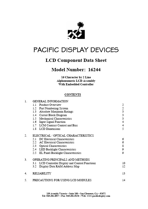
CONTENTS
1. GENERAL INFORMATION
1.1 Product Overview
2
1.2 Part Numbering System
2
1.3 Absolute Maximum Ratings
3
1.4 Circuit Block Diagram
3
1.5 Mechanical Cha
tC tr tf tW tSU th tD tDH
Min.
500 ----220 40 10 --20
Typ.
-----------------
Max.
--25 25 ------120 ---
Unit
V
Supply current for logic
IDD
---
---
1.38
3
mA
0°C
---
5.10
---
V
Operating voltage for LCD*
VDD-VO
25°C
---
4.50
---
V
50°C
---
4.30
---
V
Input voltage ' H ' level Input voltage ' L ' level
3
1.6 Input Signal Function
4
1.7 LCM Contrast Control and Bias
4
1.8 LCD Dimensions
5
2. ELECTRICAL / OPTICAL CHARACTERISTICS
2.1 DC Electrical Characteristics
ND516辞典机 说明书

功能特色■ 五大搜学功能(我搜→我学→我会)※ 导航搜学:只需输入关键字,即可快速搜索单词、句子、音乐文件、图片文件、图书、文件、名片。
※ 百科搜学:上至天文下至地理、人文历史、自然生物、古今中外一搜即有;快速超链接阅读,让您问一知三,知识百事通。
※ 图书搜学:经史子集、科普传记、人文哲学等万卷图书容量; 专业的图书管理搜索系统,全文检索查询阅读。
※ 单词搜学:联合多本词典进行便利、快捷、准确的中英文单词搜索查询。
※ 句子搜学:联合十万经典例句短语资料库,全面进行“单词、短语、例句”关联学习运用。
随机配件非常感谢您购买我们的产品。
当您打开包装彩盒后,首先请您检查,其中是否包含以下所有物品。
如有缺少,请到购买本机的销售商处找回您的物品。
1).ND516辞典机 .........................1台2).USB传输线 ..........................1根3).说明书...............................1本4).七号碱性电池.........................2个5).耳机 .................................1副6).三包卡 ...............................1份7).合格证...............................1份8).绒布套 ...............................1个ND516ND516■ 超强独特学习功能※ 单词学习:完整内置版权《全新大学英语词汇星火式巧记速记精练》,记忆、应用两不误,还有“智能背单词”让您轻松背单词。
※ 双向翻译:强大的双向整句翻译功能,中英整句互译,是学习中的好帮手。
※ 综合学习:内置 NP-ITECH 技术,学习内容无限精彩演绎;生动的课件更能真实反映科学事实,实验过程和研究结果。
※ 音文同步:视听新时空、疯狂脱口秀、多国会话,为英语学习者提供高音质语音听力、口语学习功能。
W981216BH中文资料

W981216BH2M × 4 BANKS × 16 BIT SDRAMPublication Release Date: October 2000- 1 - Revision A1GENERAL DESCRIPTIONW981216BH is a high-speed synchronous dynamic random access memory (SDRAM), organized as 2M words × 4 banks × 16 bits. Using pipelined architecture and 0.175 µm process technology, W981216BH delivers a data bandwidth of up to 143M words per second (-7). To fully comply with the personal computer industrial standard, W981216BH is sorted into three speed grades: -7, -75 and -8H. The -7 is compliant to the 143 MHz/CL3 or PC133/CL2 specification, the -75 is compliant to the PC133/CL3 specification, the -8H is compliant to the PC100/CL2 specificationAccesses to the SDRAM are burst oriented. Consecutive memory location in one page can be accessed at a burst length of 1, 2, 4, 8 or full page when a bank and row is selected by an ACTIVE command. Column addresses are automatically generated by the SDRAM internal counter in burst operation. Random column read is also possible by providing its address at each clock cycle. The multiple bank nature enables interleaving among internal banks to hide the precharging time.By having a programmable Mode Register, the system can change burst length, latency cycle, interleave or sequential burst to maximize its performance. W981216BH is ideal for main memory in high performance applications.FEATURES• 3.3V ±0.3V Power Supply • Up to 143 MHz Clock Frequency• 2,097,152 Words × 4 banks × 16 bits organization • Auto Refresh and Self Refresh • CAS Latency: 2 and 3• Burst Length: 1, 2, 4, 8, and full page • Burst Read, Single Writes Mode • Byte Data Controlled by DQM • Power-Down Mode• Auto-precharge and Controlled Precharge • 4K Refresh cycles / 64 mS • Interface: LVTTL• Packaged in TSOP II 54 pin, 400 mil - 0.80KEY PARAMETERSSYM.DESCRIPTIONMIN. /MAX.-7(PC133, CL2)-75(PC133, CL3)-8H (PC100)t CK Clock Cycle Time Min. 7 nS 7.5 nS 8 nS t AC Access Time from CLK Max. 5.4 nS 5.4 nS 6 nS t RP Precharge to Active Command Min. 15 nS 20 nS 20 nS t RCD Active to Read/Write Command Min. 15 nS 20 nS 20 nS I CC1 Operation Current (Single bank) Max. 80 mA 75 mA 70 mA I CC4 Burst Operation Current Max. 100 mA 95 mA 90 mA I CC6Self-Refresh CurrentMax.2 mA2 mA2 mAW981216BH- 2 -PIN CONFIGURATIONW981216BHPublication Release Date: October 2000- 3 - Revision A1PIN DESCRIPTIONW981216BH- 4 -BLOCK DIAGRAMW981216BHPublication Release Date: October 2000- 5 - Revision A1ABSOLUTE MAXIMUM RATINGSPARAMETERSYMBOLRATINGUNITInput/Output Voltage V IN, V OUT -0.3 − V CC +0.3 V Power Supply Voltage V CC , V CCQ -0.3 − 4.6 VOperating Temperature T OPR 0 − 70 °C Storage Temperature T STG -55 − 150 °C Soldering Temperature (10s) T SOLDER 260 °CPower DissipationP D 1 W Short Circuit Output CurrentI OUT50mANote: Exposure to conditions beyond those listed under Absolute Maximum Ratings may adversely affect the life and reliabilityof the device.RECOMMENDED DC OPERATING CONDITIONS(T A = 0 to 70°C)PARAMETER SYMBOL MIN. TYP. MAX. UNITPower Supply Voltage V CC 3.0 3.3 3.6 V Power Supply Voltage (for I/O Buffer)V CCQ 3.0 3.3 3.6 V Input High Voltage V IH 2.0 - V CC +0.3 V Input Low VoltageV IL-0.3-0.8VNote: V IH (max) = V CC / V CC Q+1.2V for pulse width < 5 nS V IL (min) = V SS / V SS Q-1.2V for pulse width < 5 nSCAPACITANCE(V CC = 3.3V, f = 1 MHz, T A = 25°C)Note: These parameters are periodically sampled and not 100% tested.W981216BH- 6 -AC CHARACTERISTICS AND OPERATING CONDITION(Vcc = 3.3V ± 0.3V, T A = 0° to 70°C; Notes: 5, 6, 7, 8)PARAMETERSYM.-7(PC133, CL2)-75(PC133, CL3)-8H (PC100)UNITMIN.MAX.MIN.MAX.MIN.MAX.Ref/Active to Ref/Active Command Periodt RC 57 65 68 Active to precharge Command Periodt RAS 42 10000045 10000048 100000nS Active to Read/Write Command Delay Timet RCD 15 20 20 Read/Write(a) toRead/Write(b)Command Period t CCD 1 1 1 Cycle Precharge to Active Command Periodt RP 15 20 20 Active(a) to Active(b) Command Periodt RRD 15 15 20 Write Recovery Time CL* = 2 t WR 7.5 10 10CL* = 3 7 7.5 8 CLK Cycle Time CL* = 2 t CK7.5 1000 10 1000 10 1000CL* = 3710007.5100081000CLK High Level width t CH 2.5 2.5 3 CLK Low Level widtht CL2.52.53Access Time from CLKCL* = 2 t AC5.4 6 6CL* = 35.4 5.4 6 nS Output Data Hold Timet OH 3 3 3 Output Data High Impedance Time t HZ 3 7 3 7.5 3 8 Output Data Low Impedance Time t LZ 0 0 0 Power Down Mode Entry Time t SB 0 7 0 7.5 0 8 Transition Time of CLK (Rise and Fall) t T 0.5 10 0.5 10 0.5 10 Data-in Set-up Time t DS 1.5 1.5 2 Data-in Hold Time t DH 0.8 0.8 1 Address Set-up Time t AS 1.5 1.5 2 Address Hold Time t AH 0.8 0.8 1 CKE Set-up Time t CKS 1.5 1.5 2 CKE Hold Time t CKH 0.8 0.8 1 Command Set-up Time t CMS 1.5 1.5 2 Command Hold Time t CMH 0.8 0.8 1 Refresh Timet REF 64 64 64 mS Mode register Set Cycle Timet RSC141516nS*CL = CAS LatencyW981216BHPublication Release Date: October 2000- 7 - Revision A1DC CHARACTERISTICS(V CC = 3.3V ± 0.3V, T A = 0°− 70°C)PARAMETERSYMBOL MIN. MAX. UNIT NOTESInput Leakage Current(0V ≤ V IN ≤ V CC , all other pins not under test = 0V) I I(L)-55µAOutput Leakage Current(Output disable , 0V ≤ V OUT ≤ V CCQ ) I O(L)-55µALVTTL Output ″H ″ Level Voltage (I OUT = -2 mA )V OH2.4-VLVTTL Output ″L ″ Level Voltage (I OUT = 2 mA )V OL-0.4VW981216BH- 8 -Notes:1. Operation exceeds "ABSOLUTE MAXIMUM RATING" may cause permanent damage to the devices.2. All voltages are referenced to V SS3. These parameters depend on the cycle rate and listed values are measured at a cycle rate with the minimum values of t CK and t RC .4. These parameters depend on the output loading conditions. Specified values are obtained with output open.5. Power up sequence is further described in the "Functional Description" section.6. AC Testing ConditionsOutput Reference Level 1.4V/1.4V Output Load See diagram belowInput Signal Levels2.4V/0.4V Transition Time (Rise and Fall) of Input Signal2 nS Input Reference Level1.4V7. Transition times are measured between V IH and V IL .8. t HZ defines the time at which the outputs achieve the open circuit condition and is not referenced to output level.W981216BHPublication Release Date: October 2000- 9 - Revision A1OPERATION MODEFully synchronous operations are performed to latch the commands at the positive edges of CLK. Table 1 shows the truth table for the operation commands. Table 1 Truth Table (Note (1), (2))Notes:(1) v = valid x = Don't care L = Low Level H = High Level (2) CKEn signal is input level when commands are provided.CKEn-1 signal is the input level one clock cycle before the command is issued. (3) These are state of bank designated by BS0, BS1 signals. (4) Device state is full page burst operation.(5) Power Down Mode can not be entered in the burst cycle.When this command asserts in the burst cycle, device state is clock suspend mode.W981216BH- 10 -FUNCTIONAL DESCRIPTIONPower Up and InitializationThe default power up state of the mode register is unspecified. The following power up and initialization sequence need to be followed to guarantee the device being preconditioned to each user specific needs.During power up, all Vcc and VccQ pins must be ramp up simultaneously to the specified voltage when the input signals are held in the "NOP" state. The power up voltage must not exceed V C C +0.3V on any of the input pins or Vcc supplies. After power up, an initial pause of 200 µS is required followed by a precharge of all banks using the precharge command. To prevent data contention on the DQ bus during power up, it is required that the DQM and CKE pins be held high during the initial pause period. Once all banks have been precharged, the Mode Register Set Command must be issued to initialize the Mode Register. An additional eight Auto Refresh cycles (CBR) are also required before or after programming the Mode Register to ensure proper subsequent operation.Programming Mode RegisterAfter initial power up, the Mode Register Set Command must be issued for proper device operation. All banks must be in a precharged state and CKE must be high at least one cycle before the Mode Register Set Command can be issued. The Mode Register Set Command is activated by the low signals of RAS, CAS, CS and WE at the positive edge of the clock. The address input data during this cycle defines the parameters to be set as shown in the Mode Register Operation table. A new command may be issued following the mode register set command once a delay equal to t RSC has elapsed. Please refer to the next page for Mode Register Set Cycle and Operation Table.Bank Activate CommandThe Bank Activate command must be applied before any Read or Write operation can be executed. The operation is similar to RAS activate in EDO DRAM. The delay from when the Bank Activate command is applied to when the first read or write operation can begin must not be less than the RAS to CAS delay time (t RCD ). Once a bank has been activated it must be precharged before another Bank Activate command can be issued to the same bank. The minimum time interval between successive Bank Activate commands to the same bank is determined by the RAS cycle time of the device (t RC ). The minimum time interval between interleaved Bank Activate commands (Bank A to Bank B and vice versa) is the Bank to Bank delay time (t RRD ). The maximum time that each bank can be held active is specified as t RAS (max).Read and Write Access ModesAfter a bank has been activated , a read or write cycle can be followed. This is accomplished by setting RAS high and CAS low at the clock rising edge after minimum of t RCD delay. WE pin voltage level defines whether the access cycle is a read operation (WE high), or a write operation (WE low). The address inputs determine the starting column address.Reading or writing to a different row within an activated bank requires the bank be precharged and a new Bank Activate command be issued. When more than one bank is activated, interleaved bank Read or Write operations are possible. By using the programmed burst length and alternating the access and precharge operations between multiple banks, seamless data access operation among many different pages can be realized. Read or Write Commands can also be issued to the same bank or between active banks on every clock cycle.W981216BHPublication Release Date: October 2000- 11 - Revision A1Burst Read CommandThe Burst Read command is initiated by applying logic low level to CS and CAS while holding RAS and WE high at the rising edge of the clock. The address inputs determine the starting column address for the burst. The Mode Register sets type of burst (sequential or interleave) and the burst length (1, 2, 4, 8, full page) during the Mode Register Set Up cycle. Table 2 and 3 in the next page explain the address sequence of interleave mode and sequential mode.Burst Write CommandThe Burst Write command is initiated by applying logic low level to CS, CAS and WE while holding RAS high at the rising edge of the clock. The address inputs determine the starting column address. Data for the first burst write cycle must be applied on the DQ pins on the same clock cycle that the Write Command is issued. The remaining data inputs must be supplied on each subsequent rising clock edge until the burst length is completed. Data supplied to the DQ pins after burst finishes will be ignored.Read Interrupted by a ReadA Burst Read may be interrupted by another Read Command. When the previous burst is interrupted, the remaining addresses are overridden by the new read address with the full burst length. The data from the first Read Command continues to appear on the outputs until the CAS latency from the interrupting Read Command the is satisfied.Read Interrupted by a WriteTo interrupt a burst read with a Write Command, DQM may be needed to place the DQs (output drivers) in a high impedance state to avoid data contention on the DQ bus. If a Read Command will issue data on the first and second clocks cycles of the write operation, DQM is needed to insure the DQs are tri-stated. After that point the Write Command will have control of the DQ bus and DQM masking is no longer needed.Write Interrupted by a WriteA burst write may be interrupted before completion of the burst by another Write Command. When the previous burst is interrupted, the remaining addresses are overridden by the new address and data will be written into the device until the programmed burst length is satisfied.Write Interrupted by a ReadA Read Command will interrupt a burst write operation on the same clock cycle that the Read Command is activated. The DQs must be in the high impedance state at least one cycle before the new read data appears on the outputs to avoid data contention. When the Read Command is activated, any residual data from the burst write cycle will be ignored.Burst Stop CommandA Burst Stop Command may be used to terminate the existing burst operation but leave the bank open for future Read or Write Commands to the same page of the active bank, if the burst length is full page. Use of the Burst Stop Command during other burst length operations is illegal. The Burst Stop Command is defined by having RAS and CAS high with CS and WE low at the rising edge of the clock. The data DQs go to a high impedance state after a delay which is equal to the CAS Latency in a burstW981216BH- 12 -read cycle interrupted by Burst Stop. If a Burst Stop Command is issued during a full page burst write operation, then any residual data from the burst write cycle will be ignored.Addressing Sequence of Sequential ModeA column access is performed by increasing the address from the column address which is input to the device. The disturb address is varied by the Burst Length as shown in Table 2.Table 2 Address Sequence of Sequential ModeAddressing Sequence of Interleave ModeA column access is started in the input column address and is performed by inverting the address bit in the sequence shown in Table 3.Table 3 Address Sequence of Interleave ModeW981216BHPublication Release Date: October 2000- 13 - Revision A1Auto-Precharge CommandIf A10 is set to high when the Read or Write Command is issued, then the auto-precharge function is entered. During auto-precharge, a Read Command will execute as normal with the exception that the active bank will begin to precharge automatically before all burst read cycles have been completed. Regardless of burst length, it will begin a certain number of clocks prior to the end of the scheduled burst cycle. The number of clocks is determined by CAS latency.A Read or Write Command with auto-precharge can not be interrupted before the entire burst operation is completed. Therefore, use of a Read, Write, or Precharge Command is prohibited during a read or write cycle with auto-precharge. Once the precharge operation has started, the bank cannot be reactivated until the Precharge time (t RP ) has been satisfied. Issue of Auto-Precharge command is illegal if the burst is set to full page length. If A10 is high when a Write Command is issued, the Write with Auto-Precharge function is initiated. The SDRAM automatically enters the precharge operation one clock delay from the last burst write cycle. This delay is referred to as Write t W R . The bank undergoing auto-precharge can not be reactivated until t W R and t RP are satisfied. This is referred to as t DAL , Data-in to Active delay (t DAL = t W R + t RP ). When using the Auto-precharge Command, the interval between the Bank Activate Command and the beginning of the internal precharge operation must satisfy t RAS (min).Precharge CommandThe Precharge Command is used to precharge or close a bank that has been activated. The Precharge Command is entered when CS, RAS and WE are low and CAS is high at the rising edge of the clock. The Precharge Command can be used to precharge each bank separately or all banks simultaneously. Three address bits, A10, BS0, and BS1, are used to define which bank(s) is to be precharged when the command is issued. After the Precharge Command is issued, the precharged bank must be reactivated before a new read or write access can be executed. The delay between the Precharge Command and the Activate Command must be greater than or equal to the Precharge time (t RP ).Self Refresh CommandThe Self Refresh Command is defined by having CS, RAS, CAS and CKE held low with WE high at the rising edge of the clock. All banks must be idle prior to issuing the Self Refresh Command. Once the command is registered, CKE must be held low to keep the device in Self Refresh mode. When the SDRAM has entered Self Refresh mode all of the external control signals, except CKE, are disabled. The clock is internally disabled during Self Refresh Operation to save power. The device will exit Self Refresh operation after CKE is returned high. A minimum delay time is required when the device exits Self Refresh Operation and before the next command can be issued. This delay is equal to the t AC cycle time plus the Self Refresh exit time.If, during normal operation, AUTO REFRESH cycles are issued in bursts (as opposed to being evenly distributed), a burst of 4,096 AUTO REFRESH cycles should be completed just prior to entering and just after exiting the self refresh mode.Power Down ModeThe Power Down mode is initiated by holding CKE low. All of the receiver circuits except CKE are gated off to reduce the power. The Power Down mode does not perform any refresh operations, therefore the device can not remain in Power Down mode longer than the Refresh period (t REF ) of the device.W981216BH- 14 -The Power Down mode is exited by bringing CKE high. When CKE goes high, a No Operation Command is required on the next rising clock edge, depending on t CK . The input buffers need to be enabled with CKE held high for a period equal to t CKS (min) + t CK (min).No Operation CommandThe No Operation Command should be used in cases when the SDRAM is in a idle or a wait state to prevent the SDRAM from registering any unwanted commands between operations. A No Operation Command is registered when CS is low with RAS, CAS, and WE held high at the rising edge of the clock. A No Operation Command will not terminate a previous operation that is still executing, such as a burst read or write cycle.Deselect CommandThe Deselect Command performs the same function as a No Operation Command. Deselect Command occurs when CS is brought high, the RAS, CAS, and WE signals become don't cares.Clock Suspend ModeDuring normal access mode, CKE must be held high enabling the clock. When CKE is registered low while at least one of the banks is active, Clock Suspend Mode is entered. The Clock Suspend mode deactivates the internal clock and suspends any clocked operation that was currently being executed. There is a one clock delay between the registration of CKE low and the time at which the SDRAM operation suspends. While in Clock Suspend mode, the SDRAM ignores any new commands that are issued. The Clock Suspend mode is exited by bringing CKE high. There is a one clock cycle delay from when CKE returns high to when Clock Suspend mode is exited.W981216BHPublication Release Date: October 2000- 15 - Revision A1TIMING WAVEFORMSCommand Input TimingW981216BH- 16 -Timing Waveforms, continuedRead TimingW981216BHPublication Release Date: October 2000- 17 - Revision A1Timing Waveforms, continuedControl Timing of Input / Output DataW981216BH- 18 -Timing Waveforms, continuedMode Register Set CycleW981216BHPublication Release Date: October 2000- 19 - Revision A1OPERATING TIMING EXAMPLEInterleaved Bank Read (Burst Length = 4, CAS Latency = 3)t RCt RASt RPt RASt RCD t RCDt RRDRAaRBdW981216BH- 20 -Operating Timing Example, continedInterleaved Bank Read (Burst Length = 4, CAS Latency = 3, Autoprecharge)(CLK = 100 MHz)t RCt RASt RPt RPt RCDt RRD t RRDW981216BHPublication Release Date: October 2000- 21 - Revision A1Operating Timing Example, continedInterleaved Bank Read (Burst Length = 8, CAS Latency = 3)t RRDW981216BH- 22 -Operating Timing Example, continedInterleaved Bank Read (Burst Length = 8, CAS Latency = 3, Autoprecharge)W981216BHPublication Release Date: October 2000- 23 - Revision A1Operating Timing Example, continedInterleaved Bank Write (Burst Length = 8)RRDW981216BH- 24 -Operating Timing Example, continedInterleaved Bank Write (Burst Length = 8, Autoprecharge)W981216BHPublication Release Date: October 2000- 25 - Revision A1Operating Timing Example, continedPage Mode Read (Burst Length = 4, CAS Latency = 3)W981216BH- 26 -Operating Timing Example, continedPage Mode Read / Write (Burst Length = 8, CAS Latency = 3)W981216BHPublication Release Date: October 2000- 27 - Revision A1Operating Timing Example, continedAuto Precharge Read (Burst Length = 4, CAS Latency = 3)(CLK = 100 MHz)CLKDQCKEDQMA0-A9,A11A10BS1WECASRASCSBS0t RCt RCDW981216BH- 28 -Operating Timing Example, continedAuto Precharge Write (Burst Length = 4)t RCt RP t RPW981216BHPublication Release Date: October 2000- 29 - Revision A1Operating Timing Example, continedAuto Refresh Cycle(CLK = 100 MHz)All Banks Prechage Auto RefreshAuto Refresh (Arbitrary Cycle)t RC t RCW981216BH- 30 -Operating Timing Example, continedSelf Refresh Cyclet SBW981216BHPublication Release Date: October 2000- 31 - Revision A1Operating Timing Example, continedBurst Read and Single Write (Burst Length = 4, CAS Latency = 3)t RCDW981216BH- 32 -Operating Timing Example, continedPowerDown Modet SBNOPW981216BHPublication Release Date: October 2000- 33 - Revision A1Operating Timing Example, continedAutoprecharge Timing (Read Cycle)APAPActActQ0Q6Q7t RPW981216BH- 34 -Operating Timing Example, continedAutoprecharge Timing (Write Cycle)D1D3D7(1) CAS Latency=2When the Auto precharge command is asserted, the period from Bank Activate command to the start of internal precgarging must be at least tRAS (min).represents the Write with Auto precharge command.represents the start of internal precharging.represents the Bank Activate command.Note )W981216BHPublication Release Date: October 2000- 35 - Revision A1Operating Timing Example, continedTiming Chart of Read to Write CycleTiming Chart of Write to Read CycleW981216BH- 36 -Operating Timing Example, continedTiming Chart of Burst Stop Cycle (Burst Stop Command)Timing Chart of Burst Stop Cycle (Precharge Command)PRCGW981216BHPublication Release Date: October 2000- 37 - Revision A1Operating Timing Example, continedCKE/DQM Input Timing (Write Cycle)W981216BH- 38 -Operating Timing Example, continedCKE/DQM Input Timing (Read Cycle)W981216BHPublication Release Date: October 2000- 39 - Revision A1Operating Timing Example, continedSelf Refresh/Power Down Mode Exit TimingW981216BH- 40 -PACKAGE DIMENSION54L TSOP (II)-400 milW981216BHPublication Release Date: October 2000- 41 - Revision A1No. 4, Creation Rd. III,/11F, No. 115, Sec. 3, MinUnit 9Winbond Memory Lab.TEL: 408HeadquartersScience -Based Industrial Park,Hsinchu, TaiwanTEL: 886-3-5770066FAX: 886-3-5796096Voice & Fax -on -demand: 886-2-27197006Taipei Office-Sheng East Rd.,Taipei, TaiwanTEL: 886-2-27190505FAX: 886-2-27197502 Winbond Electronics (H.K.) Ltd.-15, 22F, Millennium City, No. 378 Kwun Tong Rd; Kowloon, Hong Kong TEL: 852-********FAX: 852-********Winbond Electronics North America Corp.Winbond Microelectronics Corp.Winbond Systems Lab.2727 N. First Street, San Jose,CA 95134, U.S.A.-9436666FAX: 408-5441798Note: All data and specifications are subject to change withou t notice.。
ICN2516_英文规格书_en2011
ICN2516 HIGH POWER FACTOR 4-CH HVLDOGENERAL DESCRIPTIONThe IC is capable of driving multiple series connected LEDs. The IC sense rectified AC input source voltage to modulate LED current which can in phase input voltage to implement high power factor and high efficiency. The IC is a high voltage process chip with internal regulator to generate bios voltage which supports IC internal circuit. The IC also has internal power switch to minimize external components.The package of the IC is TSSOP-16. Which suitable for LED lighting like MR-16, E-17, E27…and so on applications.FEATURESz Low Quiescent Currentz No Inductor Component Requiredz Internal 500V NMOS Switchz High Power Factor Applicationz High Efficiency (up to 85%)z Programmable LED Currentz OverTemperatureProtectionRoHS Compliant and 100% Lead (Pb)-Free and Green (Halogen Free with Commercial StandardSIMPLIFIED APPLICATION CIRCUITABSOLUTE MAXIMUM RATINGSParameter Symbol Ratings UnitsHigh Voltage Input and LED String SwitchV IN / V SW0/V SW1/ V SW2/ V SW3500 VIC Regulation Voltage input V CC 36 VSwitch Current Rating I SW 0.1 AOther I/O Pin Voltage V IO 7 V Junction TemperatureT J +150 °CPower DissipationTSSOP-16P D 2000 mW Operating Ambient TemperatureT OPR -40 ~ +125 °C Storage TemperatureT STG -55 ~ +150 °C Lead Temperature (soldering, 10sec)+260°CNote :* The power dissipation values are based on the condition that junction temperature T J and ambient temperature T A difference is 100°C.* Stresses beyond those listed under “absolute maximum ratings” may cause permanent damage to the device. These are stress ratings only, and function operation of the device at these or any other conditions beyond those indicated under “recommended operating conditions” is not implied. Exposure to absolute-maximum -rated conditions for extended periods may affect device reliability.*Stresses exceeding Maximum Ratings may damage the device. Maximum Ratings are stress ratings only. Functional operation above the recommended operating conditions is not implied. Extended exposure to stresses above the Recommended Operating Conditions may affect device reliability.ELECTRICAL CHARACTERISTICSSymbol Parameter Test Conditions MinTyp Max UnitV IN High voltage input Vin rising500 VV CCInternal regulation voltageVin rising measure V CC 9 VI SET0 First step current SW1 turn on; VS1 < 0.51V 1580/Rset mA I SET1 First step current SW1 turn on; VS1 > 0.51V;VS2<1.02V1580/RsetmA I SET2 Second step current SW2 turn on; VS1 > 1.02V andVS2<1.02V2080/Rset mA I SET3 Third step current SW2 turn on; VS1 > 1.02V andVS2>1.02V2580/RsetmAT TST Thermal Shutdown Temperature 150°C T TSHThermal Shutdown Hysteresis40°CFUNCTION BLOCK DIAGRAMPIN DESCRIPTIONSymbol1 VS12 VS23 4,7/EP GND 5 8PACKAGE OUTLINE A) TSSOP-16REFLOW CONDITION (IR/Convection or VPR Reflow)CLASSIFICATION REFLOW PROFILESProfile FeaturePb-Free / Green AssemblyAverage ramp-up rate (T L to T P )3°C/second max Preheat- Temperature Min (Tsmin) - Temperature Max (Tsmax) - Time (min to max) (ts) 150°C 200°C60-180 seconds Time maintained above: - Temperature (T L ) - Time (t L )217°C60-150 seconds Peak/Classification Temperature (Tp) See table 1 Time within 5°C of actual Peak Temperature (tp)20-40 seconds Ramp-down Rate6°C/second max Time 25°C to Peak Temperature8 minutes maxNotes :1) All temperatures refer to topside of the package. 2) Measured on the body surface.CLASSIFICATION REFLOW PROFILES (CONTINUED) Table 1. Pb-free / Green Process – Package Classification Reflow TemperaturesPackage Thickness Volume mm³<350Volume mm³350~2000Volume mm³2000≧<2.5 mm260 +0°C* 260 +0°C* 260 +0°C*1.6-2.5 mm260 +0°C*250 +0°C*245 +0°C*≧2.5 mm250 +0°C* 245 +0°C* 245 +0°C* Notes:* Tolerance: The device manufacturer/supplier shall assure process compatibility up to and including the stated classification temperature (this means Peak reflow temperature +0°C. For example 260°C+0°C) at the rated MSL level.IMPORTANT NOTICEChipone Technology (Beijing) Co., Ltd. (Chipone) reserves the right to make changes to their products or to discontinue any product or service without notice, and advise customers to obtain the latest version of relevant information to verify, before placing orders, that information being relied on is current and complete. All products are sold subject to the terms and conditions of sale supplied at the time of order acknowledgement, including those pertaining to warranty, patent infringement, and limitation of liability.Chipone warrants performance of its semiconductor products to the specifications applicable at the time of sale in accordance with Chipone’s standard warranty. Testing and other quality control techniques are utilized to the extent Chipone deems necessary to support this warranty. Specific testing of all parameters of each device is not necessarily performed, except those mandated by government requirements.CERTAIN APPLICATIONS USING SEMICONDUCTOR PRODUCTS MAY INVOLVE POTENTIAL RISKS OF DEATH, PERSONAL INJURY, OR SEVERE PROPERTY OR ENVIRONMENTAL DAMAGE (“CRITICAL APPLICATIONS”). CHIPONE SEMICONDUCTOR PRODUCTS ARE NOT DESIGNED, AUTHORIZED, OR WARRANTED TO BE SUITABLE FOR USE IN LIFE-SUPPORT DEVICES OR SYSTEMS OR OTHER CRITICAL APPLICATIONS. INCLUSION OF CHIPONE PRODUCTS IN SUCH APPLICATIONS IS UNDERSTOOD TO BE FULLY AT THE CUSTOMER’S RISK.In order to minimize risks associated with the customer’s applications, adequate design and operating safeguards must be provided by the customer to minimize inherent or procedural hazards.Chipone assumes no liability for applications assistance or customer product design. Chipone does not warrant or represent that any license, either express or implied, is granted under any patent right, copyright, mask work right, or other intellectual property right of Chipone covering or relating to any combination, machine, or process in which such semiconductor products or services might be.or are used. Chipone’s publication of information regarding any third party’s products or services does not constitute Chipone’s approval, warranty or endorsement thereof.◎Chipone Technology (Beijing) Co., Ltd.Copyright 2011,。
MEMORY存储芯片TMS2516JDL中文规格书
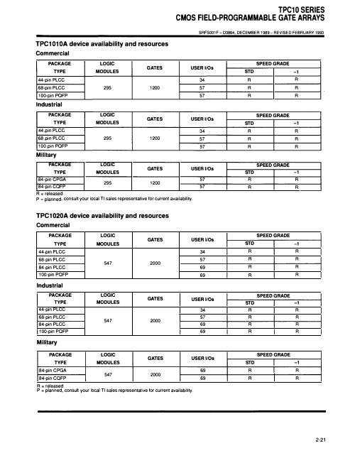
TPC10 SERIES CMOS FIELD-PROGRAMMABLE GATE ARRAYSSRFS001F-D3864, DECEMBER 1989-REVISED FEBRUARY 1993TPC1010A device availability and res 。
urces CommercialPACKAGELOGIC GATES USER I/。
s TYPEMODULES 44-pin P LCC34 68-pin P LCC295 1200 57 100-pin P OFP57 IndustrialPACKAGELOGIC GATES USER I/Os TYPEMODULES 44 pin P LCC34 68 pin P LCC295 1200 57 100 pin P QFP57 MilitaryPACKAGELOGIC TYPEM 。
DULES GATES USER I/Os 84-pinCPGA572951200 84-pin C QFP 57 R = released P = planned , consult your local Tl sales representative for current availability. TPC1020A device availability and res 。
urces CommercialPACKAGETYPE44 pin P LCC68-pin P LCC84 pin P LCC100-pin P QFPIndustrialPACKAGETYPE44-pin P LCC68-pin P LCC84 pin P LCC100-pin P QFPMilitaryPACKAGETYPE84-pin C PGA84-pin C QFP R = released LOGIC M 。
DULES 547 LOGIC M 。
DULES 547 L 。
Kleen Sweep 25W Sweeper - Parts Manual

2
11
01176350 Cap
1
12
01176520 Hinge outer
2
13
01176510 Hinge inner
2
14
01176360 Cap
1
Remarks
Parts Manual - Kleen Sweep 25W Sweeper
Page 12
Filter system part 1
Qty.
Remarks
2
2
1
4
1
1
1
1
1
1
1
1
2
4
1
Charging cable
Parts Manual - Kleen Sweep 25W Sweeper
Page 10
Steering handle
Rev.B 06/12
Parts Manual - Kleen Sweep 25W Sweeper
Page 11
Steering handle (99625820BT40)
Rev.B 06/12
Item
Spare part number
Description
Qty.
1
01275090 Socket head screw
4
2
01176500 Mounting outer
1
3
01176480 Limit switch
Parts Manual Kleen Sweep 25W Sweeper
Parts Manual - Kleen Sweep 25W Sweeper
Page 2
Table of Contents
台湾制造DUAL INPUT RTD 四位数数字温度计说明书

MADE IN TAIWANOPERATING INSTRUCTIONSHH804UDUAL INPUT RTD THERMOMETERINTRODUCTION This instrument is a 4_digit,compact-sized portable digital thermometer designed to use external 100_Platinum RTD as temperature sensor.Tem-perature indication follows Reference Temperature/Resistance Tables (Pt385for European Curve,Alpha=.00385.Pt3926for American Curve,Al pha=.003926. Pt3916 for Japan Curve, Alpha=.003916.)SAFETY INFORMATIONIt is recommended that you read the safety and operation instructions before using the thermometer.WARNINGTo avoid electrical shock, do not use this instrument when working voltagesat the measurement surface over 24V AC or DC.WARNINGTo avoid damage or burns, do not take temperature measurements in micro-wave ovens.ENVIRONMENTALAmbient Operating Ranges:0°C to 50°C (32°F to 122°F) <70% R.H.Storage Temperature:-20°C to 60°C (-4°F to 140°F) <80% R.H.GENERALDisplay:4_ digit liquid crystal display (LCD) with maximum reading of 19999Overload:“----.-“ or “OL” is display.Battery:1.5V x 4 PCS (SIZE AAA) R03P.Battery Life:200 hours typical with carbon zinc battery Auto power off: 30 minutes Dimensions:160mm(H) x83mm(W) x 38mm(D)Weight:Approx. 255g including batteries.SPECIFICATIONSELECTRICALTemperature Scale: Celsius or Fahrenheit user-selectable Measurement Range:Pt385(100_) -200°C to 800°C, (-328°F to 1472°F)Pt3916/Pt3926(100_) -200°C to 630°C, (-328°F to 1166°F)Resolution:0.1°C or 0.2°F Accuracy:Accuracy is specified for operating temperatures over the range of 18°C to 28°C (64°F to 82°F), for 1 year, not including RTD probe error.±(0.05% rdg + 0.2°C) on °C scale ±(0.05% rdg + 0.4°F) on °F scale Temperature Coefficient:0.1 times the applicable accuracy specification per °C from 0°C to 18°C and 28°C to 50°C (32°F to 64°F and 82°F to 122°F).Input Protection:24V dc or 24V ac rms maximum input voltage on any combination of input pins.Maximum Differential Common Mode Voltage (Maximum Voltage be-tween T1 and T2 during measurement): 1volt.Reading Rate: 1sample/second.Input Connector:Accepts 4 pin mini-DIN connectors.OPERATING INSTRUCTIONS1.Power ButtonThebutton turns the thermometer on or off. In the SET mode the unit cannot be powered off. Exit the SET mode to power off.APO function modePress “”power button for more than 6seconds to disable auto power function. The display will show “APO OFF”.2.°C/°F Selecting the Temperature Scale (Main display)Readings are displayed in either degrees Celsius(°C) or degrees Fahren-heit(°F). When the thermometer is turned on, it is set to the temperature scale that was in use when the thermometer was last turned off. To change the temperature scale, press the °C/°F key.3. “ ” Display Back-LightPress the “ ” key to turn on or turn off the back light.4. T1 T2/T1-T2 Main display Input SelectionThe input selection button determines which input is shown on the display;T1,T2or the difference between the two probes (T1-T2).When thermometer is turned on, it is set to T1.5. TYPE(Pt385/Pt3926/Pt3916) Input RTD Probe Select (Main display)The TYPE button selects the RTD curve to use for the input currently shown.When the thermometer is turned on,it is set to the curve that selected when the thermometer was last turned off.6. MIN MAX with Time record Mode (only Main display)Press MIN MAX key to enter the MIN MAX Recording mode,(displays Maximum reading with time,Minimum reading with time and Average reading stored in recording mode).In the this mode the automatic power-off feature is disabledand key,°C/°F key,REL key,SET key,Hi/Lo Li key and main display T1T2T1-T2key,TYPE key are disabled.beeper emits a tone when a new minimum or maximum value is recorded.Push MIN MAX key to cycle through the MAX, MIN and AVG readings.If an overload is recorded,the averaging function is Stopped.In the mode,press HOLD key to stop the recording of readings,all values are zen,press again to restart recording.To prevent accidental loss of MAX and AVG data,in this mode can only be cancelled by pressing hold down the MIN MAX key for 2seconds to exit and erased recorded readings.7. REL Relative mode (only Main display)Press REL key to enter the Relative mode,zero the display,and store displayed Reading as a reference value and annunciator REL is displayed.Press REL key again to exit the relative mode.The relative value can be entered by the user.(See “SET mode”later in this manual.)When the sired Relative value has been entered,press REL key to enter the Relative mode,press SET key use set Relative value as a reference value.Press key again to exit the relative mode.In the Relative mode,the value (can >±1999.9counts)shown on the LCD is always the difference between stored reference and the present reading.8.HOLD Mode (only Main display)Press the HOLD key to enter the Data Hold mode,the “HOLD”annunciator is displayed.When HOLD mode is selected,the thermometer held the sent readings and stops all further measurements.Press the HOLD again to cancel HOLD mode causing thermometer to resume taking ureents.In the MIN/MAX recording mode,press HOLD key to stop the cording.Press HOLD key again to resume recording.(Previously recorded read are not erased).9. SET mode (Relative value set, Time set and Hi/Lo Limits value set)Press SET key to enter Relative values SET mode (Press ENTER key escape relative values set mode),REL set mode.====.=is displayed main display.Relative value is entered via overlay numbers,thenHH804UOMEGAnet ®On-Line ServiceInternet e-mail **************Czech Republic:Frystatska 184, 733 01 Karvina ´, Czech Republic Tel: +420 (0)59 6311899FAX: +420 (0)59 6311114Toll Free: 0800-1-66342e-mail:*****************Germany/Austria:Daimlerstrasse 26, D-75392 Deckenpfronn, Germany Tel: +49 (0)7056 9398-0 FAX: +49 (0)7056 9398-29TollFreeinGermany************e-mail:*************Servicing Europe:U.S.A. and Canada:Sales Service: 1-800-826-6342/1-800-TC-OMEGA Customer Service: 1-800-622-2378/1-800-622-BEST Engineering Service: 1-800-872-9436/1-800-USA-WHEN U.S.A.: ISO 9001 Certified One Omega Drive, Box 4047Stamford, CT 06907-0047Tel: (203) 359-1660FAX: (203) 359-7700e-mail:**************Servicing North America:For immediate technical or application assistance:Mexico:En Espan~ol: (001) 203-359-7803FAX: (001) 203-359-7807e-mail:*******************************.mxUnited Kingdom ISO 9002 Certified One Omega DriveRiver Bend Technology Centre Northbank, Irlam Manchester M44 5BD United KingdomTel: +44 (0)161 777 6611 FAX: +44 (0)161 777 6622Toll Free in United Kingdom: 0800-488-488e-mail:**************.ukCanada:976 BergarLaval (Quebec) H7L 5A1, Canada Tel: (514) 856-6928FAX: (514) 856-6886e-mail:*************Where Do I Find Everything I Need for Process Measurement and Control?OMEGA…Of Course!Shop online at M4501/0607TEMPERATUREⅪߜThermocouple, RTD & ThermistorProbes, Connectors, Panels &Assemblies ⅪߜWire: Thermocouple, RTD &Thermistor ⅪߜCalibrators & Ice Point References ⅪߜRecorders, Controllers & ProcessMonitors ⅪߜInfrared PyrometersPRESSURE, STRAIN AND FORCEⅪߜTransducers & Strain GagesⅪߜLoad Cells & Pressure Gages ⅪߜDisplacement Transducers ⅪߜInstrumentation & AccessoriesFLOW/LEVELⅪߜRotameters, Gas Mass Flowmeters &Flow Computers ⅪߜAir Velocity Indicators ⅪߜTurbine/Paddlewheel Systems ⅪߜTotalizers & Batch ControllerspH/CONDUCTIVITYⅪߜpH Electrodes, Testers & Accessories ⅪߜBenchtop/Laboratory Meters ⅪߜControllers, Calibrators, Simulators &Pumps ⅪߜIndustrial pH & ConductivityEquipmentDATA ACQUISITIONⅪߜData Acquisition & EngineeringSoftware ⅪߜCommunications-Based AcquisitionSystems ⅪߜPlug-in Cards for Apple, IBM &Compatibles ⅪߜDatalogging Systems ⅪߜRecorders, Printers & PlottersHEATERSⅪߜHeating CableⅪߜCartridge & Strip Heaters ⅪߜImmersion & Band Heaters ⅪߜFlexible Heaters ⅪߜLaboratory HeatersENVIRONMENTALMONITORING AND CONTROLⅪߜMetering & Control InstrumentationⅪߜRefractometers ⅪߜPumps & TubingⅪߜAir, Soil & Water Monitors ⅪߜIndustrial Water & Wastewater Treatment ⅪߜpH, Conductivity & Dissolved OxygenInstrumentsRETURN REQUESTS/INQUIRIESDirect all warranty and repair requests/inquiries to the OMEGA Customer Service Department.BEFORE RETURNING ANY PRODUCT(S) TO OMEGA, PURCHASER MUST OBTAIN AN AUTHORIZED RETURN (AR) NUMBER FROM OMEGA’S CUSTOMER SERV ICE DEPARTMENT (IN ORDER TO AV OID PROCESSING DELAYS). The assigned AR number should then be marked on the outside of the return package and on any correspondence.The purchaser is responsible for shipping charges, freight, insurance and proper packaging to prevent breakage in transit.FOR WARRANTY RETURNS, please have the following information available BEFORE contacting OMEGA:1.Purchase Order number under which the product was PURCHASED,2.Model and serial number of the product under warranty, and3.Repair instructions and/or specific problems relative to the product.FOR NON-WARRANTY REPAIRS,consult OMEGA for current repair charges. Have the following information available BEFORE contacting OMEGA:1. Purchase Order number to cover the COST of the repair,2.Model and serial number of the product, and3.Repair instructions and/or specific problems relative to the product.WARRANTY/DISCLAIMEROMEGA ENGINEERING, INC. warrants this unit to be free of defects in materials and workmanship for a period of 13 months from date of purchase. OMEGA’s WARRANTY adds an additional one (1) month grace period to the normal one (1) year product warranty to cover handling and shipping time. This ensures that OMEGA’s customers receive maximum coverage on each product.If the unit malfunctions, it must be returned to the factory for evaluation. OMEGA’s Customer Service Department will issue an Authorized Return (AR) number immediately upon phone or written request. Upon examination by OMEGA, if the unit is found to be defective, it will be repaired or replaced at no charge. OMEGA’s WARRANTY does not apply to defects resulting from any action of the purchaser, including but not limited to mishandling,improper interfacing, operation outside of design limits, improper repair, or unauthorized modification. This WARRANTY is VOID if the unit shows evidence of having been tampered with or shows evidence of having been damaged as a result of excessive corrosion; or current, heat, moisture or vibration; improper specification; misapplication; misuse or other operating conditions outside of OMEGA’s control. Components in which wear is not warranted, include but are not limited to contact points, fuses, and triacs.OMEGA is pleased to offer suggestions on the use of its various products.However, OMEGA neither assumes responsibility for any omissions or errors nor assumes liability for any damages that result from the use of its products in accordance with information provided by OMEGA, either verbal or written.OMEGA warrants only that the parts manufactured by the company will be as specified and free of defects. OMEGA MAKES NO OTHER W ARRANTIES OR REPRESENTATIONS OF ANY KIND W HATSOEVER, EXPRESSED OR IMPLIED,EXCEPT THAT OF TITLE, AND ALL IMPLIED W ARRANTIES INCLUDING ANY WARRANTY OF MERCHANTABILITY AND FITNESS FOR A PARTICULAR PURPOSE ARE HEREBY DISCLAIMED. LIMITATION OF LIABILITY: The remedies of purchaser set forth herein are exclusive, and the total liability of OMEGA with respect to this order, whether based on contract, warranty, negligence, indemnification, strict liability or otherwise, shall not exceed the purchase price of the component upon which liability is based. In no event shall OMEGA be liable for consequential,incidental or special damages.CONDITIONS: Equipment sold by OMEGA is not intended to be used, nor shall it be used: (1)as a “Basic Component” under 10 CFR 21 (NRC), used in or with any nuclear installation or activity; or (2) in medical applications or used on humans. Should any Product(s) be used in or with any nuclear installation or activity, medical application, used on humans, or misused in any way, OMEGA assumes no responsibility as set forth in our basic WARRANTY /DISCLAIMER language, and, additionally, purchaser will indemnify OMEGA and hold OMEGA harmless from any liability or damage whatsoever arising out of the use of the Product(s) in such a manner.he policy of OMEGA Engineering, Inc. to comply with all worldwide safety and EMC/EMI ations that apply. OMEGA is constantly pursuing certification of its products to thepean New Approach Directives. OMEGA will add the CE mark to every appropriate device certification.nformation contained in this document is believed to be correct, but OMEGA accepts no ty for any errors it contains, and reserves the right to alter specifications without notice.NING: These products are not designed for use in, and should not be used for, human cations.OMEGAʼs policy is to make running changes, not model changes, whenever an improvement is possible. This affords our customers the latest in technology and engineering.OMEGA is a registered trademark of OMEGA ENGINEERING, INC.© Copyright 2007 OMEGA ENGINEERING, INC. All rights reserved. This document may not be copied, photocopied, reproduced, translated, or reduced to any electronic medium or machine-readable form, in whole or in part, without the prior written consent of OMEGA ENGINEERING, INC.overlay ENTER key, stored the relative value, enter Time set mode.Time set mode,(Press ENTER key can escape Time set mode)=.===:==is displayed in second and third display.Time (hours,minutes,seconds)value is entered via overlay numbers,then press overlay ENTER key.Time start from set time value, enter Hi/Lo Limits value set mode.Hi Limit value set mode,(Press ENTER key can escape Hi Limit value set mode),====.=is displayed in main display,Hi Limit value is entered via overlay numbers,then press overlay ENTER key,stored the Hi Limit value,enter Lo Limit value set mode (Press ENTER key can escape Lo Limit value set mode).====.=is displayed in main display,Lo Limit value is entered via overlay numbers,then press overlay ENTER key,stored the Lo Limit value and exit SET mode.When the thermometer is turned on.The Relative set value and Hi/Lo Limits set value that was in use when thermometer was last turned off set values.T1/T2 T1-T2 second display Input Selectionhe input selection button determines which input is shown on the second splay;T1,T2or the difference between the two probes (T1-T2).When the ermometer is turned on, it is set to T2.TYPE(Pt385/Pt3926/Pt3916) Input RTD Probe select (second display)he TYPE button selects the RTD curve to use for the input currently own.When the thermometer is turned on,it is set to the curve that was lected when the thermometer was last turned off.Hi/Lo Limits mode (only Main display)ess the Hi/Lo Limits button to enter the Hi/Lo Limits comparative mode,hen the input temperature exceeds the Hi or Lo Limits value,the beeper mits a continuous pulse tone.Press the Hi/Lo Limits button again to exit e Hi/Lo Limits mode.TD PROBE CONNECTIONMPERATURE VS RESISTANCE TABLE(ITS90)°C Pt385Pt3926Pt3916-200°C 18.521_16.996_17.057_-100°C 60.256_59.479_59.565_0°C 100.000_100.000_100.000_100°C 138.505_139.272_139.171_200°C 175.856_177.362_177.155_300°C 212.052_214.275_213.957_400°C 247.092_250.018_249.584_500°C 280.977_284.591_284.036_600°C 313.708_317.994_317.313_700°C 345.280_--800°C 375.700_--OPERATOR MAINTENANCEWARNINGTo avoid possible electrical shock, disconnect the thermocouple connectorsfrom the thermometer before removing the cover.Battery Replacement1. Power is supplied by 4pcs 1.5V (SIZE AAA) R03P.2. The “” appears on the LCD display when replacement is needed. Toreplace battery remove screw from back of meter and lift off the battery cover.3. Remove the battery from battery contacts and replace.4. When not in use for long periods the batteries should be removed.5. Do not store in locations with high temperatures, or high humidity.CleaningPeriodically wipe the case with a damp cloth and detergent, do not use abra sives or solvents.V1. 040307。
ATEN KH2505 2516 说明书

概述 ............................................... ix
常规用语 ............................................ x
产品信息 ................................................ x
第一章 介绍
概述 .................................................... 1 功能特性 ................................................ 3 硬件需求 ................................................ 4
控制端 .............................................. 4 主机 ................................................ 4 KVM 适配器线缆 ....................................... 4 其他线缆 ............................................ 5 操作系统 ............................................ 5 产品部件 ................................................ 6 前视图 .............................................. 6 后视图 .............................................. 8 近端控制端连接 ...................................... 9
- 1、下载文档前请自行甄别文档内容的完整性,平台不提供额外的编辑、内容补充、找答案等附加服务。
- 2、"仅部分预览"的文档,不可在线预览部分如存在完整性等问题,可反馈申请退款(可完整预览的文档不适用该条件!)。
- 3、如文档侵犯您的权益,请联系客服反馈,我们会尽快为您处理(人工客服工作时间:9:00-18:30)。
4M × 4 BANKS × 16 BIT DDR SDRAMPublication Release Date: May 20, 2003 Table of Contents-1. GENERAL DESCRIPTION.........................................................................................................32. FEATURES.................................................................................................................................33. KEY PARAMETERS...................................................................................................................44. PIN CONFIGURATION...............................................................................................................55. PIN DESCRIPTION.....................................................................................................................66. BLOCK DIAGRAM......................................................................................................................77.ELECRICAL CHARACTERISTICS (8)7.1 Absolute Maximum Ratings .................................................................................................8 7.2 Recommended DC Operating Conditions............................................................................8 7.3 Capacitance.........................................................................................................................9 7.4 Leakage and Output Buffer Characteristics.........................................................................9 7.5 DC Characteristics.............................................................................................................10 7.6 AC Characteristics and Operating Condition .....................................................................11 7.7AC Test Conditions............................................................................................................13 8. OPERATION MODE.. (15)8.1 Simplified Truth Table........................................................................................................15 8.2 Function Truth Table..........................................................................................................16 8.3 Function Truth Table for CKE............................................................................................19 8.4Simplified Stated Diagram..................................................................................................20 9. FUNCTIONAL DESCRIPTION.. (21)9.1 Power Up Sequence..........................................................................................................21 9.2 Command Function............................................................................................................21 9.3 Read Operation..................................................................................................................24 9.4 Write Operation..................................................................................................................24 9.5 Precharge...........................................................................................................................24 9.6 Burst Termination...............................................................................................................25 9.7 Refresh Operation..............................................................................................................25 9.8 Power Down Mode.............................................................................................................25 9.9Mode Register Operation...................................................................................................25 10. TIMING WAVEFORMS. (29)10.1 Command Input Timing......................................................................................................29 10.2Timing of the CLK Signals (29)10.3Read Timing (Burst Length = 4) (30)10.4Write Timing (Burst Length = 4) (31)10.5DM, Data Mask (W942508CH /W942504CH) (32)10.6DM, Data Mask (W942516CH) (32)10.7Mode Register Set (MRS) Timing (33)10.8Extend Mode Register Set (EMRS) Timing (34)10.9Auto Precharge Timing (Read Cycle, CL = 2) (35)10.10Auto Precharge Timing (Write Cycle) (37)10.11Read Interrupted by Read (CL = 2, BL = 2, 4, 8) (38)10.12Burst Read Stop (BL = 8) (38)10.13Read Interrupted by Write & BST (BL = 8) (39)10.14Read Interrupted by Precharge (BL = 8) (39)10.15Write Interrupted by Write (BL = 2, 4, 8) (40)10.16Write Interrupted by Read (CL = 2, BL = 8) (40)10.17Write Interrupted by Read (CL = 2.5, BL = 4) (41)10.18Write Interrupted by Precharge (BL = 8) (41)10.19 2 Bank Interleave Read Operation (CL = 2, BL = 2) (42)10.20 2 Bank Interleave Read Operation (CL = 2, BL = 4) (42)10.21 4 Bank Interleave Read Operation (CL = 2, BL = 2) (43)10.22 4 Bank Interleave Read Operation (CL = 2, BL = 4) (43)10.23Auto Refresh Cycle (44)10.24Active Power Down Mode Entry and Exit Timing (44)10.25Precharged Power Down Mode Entry and Exit Timing (44)10.26Self Refresh Entry and Exit Timing (45)11.PACKAGE DIMENSION (46)12.REVISION HISTORY (47)Publication Release Date: May 20, 20031. GENERAL DESCRIPTIONW942516CH is a CMOS Double Data Rate synchronous dynamic random access memory (DDR SDRAM), organized as 4,194,304 words × 4 banks × 16 bits. Using pipelined architecture and 0.13 µm process technology, W942516CH delivers a data bandwidth of up to 400M words per second (-5). To fully comply with the personal computer industrial standard, W942516CH is sorted into four speed grades: -5, -6, -7, -75 The -5 is compliant to the 200 MHz/CL2.5 & CL3 specification, The -6 is compliant to the 166 MHz/CL2.5 specification, the -7 is compliant to the 143 MHz/CL2.5 or DDR266/CL2 specification, the -75 is compliant to the DDR266/CL2.5 specification.All Inputs reference to the positive edge of CLK (except for DQ, DM, and CKE). The timing reference point for the differential clock is when the CLK and CLK signals cross during a transition. And Write and Read data are synschronized with the both edges of DQS (Data Strobe).By having a programmable Mode Register, the system can change burst length, latency cycle, interleave or sequential burst to maximize its performance. W942516CH is ideal for main memory in high performance applications.2. FEATURES• 2.5V ±0.2V Power Supply for DDR266 • 2.5V ±0.2V Power Supply for DDR333 • 2.6V ±0.1V Power Supply for DDR400 • Up to 200 MHz Clock Frequency• Double Data Rate architecture; two data transfers per clock cycle • Differential clock inputs (CLK and CLK )• DQS is edge-aligned with data for Read; center-aligned with data for Write • CAS Latency: 2, 2.5 and 3 • Burst Length: 2, 4 and 8 • Auto Refresh and Self Refresh• Precharged Power Down and Active Power Down • Write Data Mask • Write Latency = 1• 8K Refresh Cycles / 64 mS • Interface: SSTL-2• Packaged in TSOP II 66-pin, 400 x 875 mil, 0.65 mm pin pitch3. KEY PARAMETERSSYMBOL DESCRIPTION MIN./MAX.-7-75 t CK Clock Cycle Time CL = 2 Min. 7.5 nS 8 nSCL = 2.5 Min. 7 nS 7.5 nS t RAS Active to Precharge Command Period Min. 45 nS 45 nS t RC Active to Ref/Active Command Period Min. 65 nS 65 nSI DD1Operation Current (Single bank) Max. 120 mA 120 mAI DD4Burst Operation Current Max. 165 mA 155 mAI DD6Self-Refresh Current Max. 3 mA 3 mASYMBOL DESCRIPTION MIN./MAX.-5-6CL = 2.5 Min. 5 nS 6 nS t CK Clock Cycle TimeCL = 3 Min. 5 nS 6 nS t RAS Active to Precharge Command Period Min. 40 nS 42 nS t RC Active to Ref/Active Command Period Min. 55 nS 60 nSI DD1Operation Current (Single bank) Max. 120 mA 120 mAI DD4Burst Operation Current Max. 165 mA 165 mAI DD6Self-Refresh Current Max. 3 mA 3 mAPublication Release Date: May 20, 20034. PIN CONFIGURATION5. PIN DESCRIPTIONPublication Release Date: May 20, 2003 6. BLOCK DIAGRAM7. ELECRICAL CHARACTERISTICS7.1 Absolute Maximum RatingsUNITRATINGPARAMETER SYMBOLInput/Output Voltage V IN, V OUT -0.3 − V DDQ +0.3 VPower Supply Voltage V DD, V DDQ -0.3 − 3.6 VOperating Temperature T OPR 0 − 70 °CStorage Temperature T STG -55 − 150 °CSoldering Temperature (10s) T SOLDER 260 °CPower Dissipation P D 1 W Short Circuit Output Current I OUT 50 mA Note: Exposure to conditions beyond those listed under Absolute Maximum Ratings may adversely affect the life and reliability of the device.7.2 Recommended DC Operating Conditions(T A = 0 to 70°C)Notes: Undershoot Limit: V IL (min) = -0.9V with a pulse width < 5 nSOvershoot Limit: V IH (max) = V DD Q +0.9V with a pulse width < 5 nSV IH (DC) and V IL (DC) are levels to maintain the current logic state.V IH (AC) and V IL (AC) are levels to change to the new logic state.Publication Release Date: May 20, 2003 7.3 Capacitance(V DD = V DDQ = 2.5V ±0.2V, f = 1 MHz, T A = 25 °C, V OUT (DC) = V DDQ /2, V OUT (Peak to Peak) = 0.2V)SYMBOL PARAMETER MIN. MAX.DELTA(MAX.) UNIT C IN Input Capacitance (except for CLK pins)2.03.00.5pFC CLK Input Capacitance (CLK pins) 2.0 3.0 0.25 pF C I/O DQ, DQS, DM Capacitance 4.0 5.0 0.5 pFC NC1 NC1 Pin Capacitance - 1.5 - pF C NC2NC2 Pin Capacitance4.05.0-pFNotes: These parameters are periodically sampled and not 100% tested.The NC2 pins have additional capacitance for adjustment of the adjacent pin capacitance. The NC2 pins have Power and Ground clamp.7.4 Leakage and Output Buffer CharacteristicsSYMBOL PARAMETER MIN. MAX. UNITS NOTES I I (L) Input Leakage Current(0V < V IN < V DDQ , All other pins not under test = 0V) -2 2 µA I O (L) Output Leakage Current(Output disabled, 0V < V OUT < V DDQ )-5 5 µAV OH Output High Voltage(under AC test load condition) V TT +0.76 - VV OL Output Low Voltage (under AC test load condition)- V TT -0.76 VI OH (DC) Output Minimum Source DC Current -15.2 - mA 4, 6 I OL (DC) Output Minimum Sink DC Current Full Strength 15.2 - mA 4, 6 I OH (DC) Output Minimum Source DC Current -10.4-mA5I OL (DC)Output Minimum Sink DC CurrentHalfStrength10.4 - mA 5CKRANDOM READ CURRENT Timing (I DD7)COMMAND DQPublication Release Date: May 20, 2003 7.6 AC Characteristics and Operating ConditionPublication Release Date: May 20, 2003 7.7 AC Test ConditionsV V DD QV IH min (AC)V REFV IL max (AC)SLEW = (V IH min (AC) - V IL max (AC)) /TT = 50 ohmsVTTA.C. TEST LOAD (A)Notes: (1) Conditions outside the limits listed under “ABSOLUTE MAXIMUM RATINGS” may cause permanent damage to thedevice.(2) All voltages are referenced to V SS , V SSQ. .( 2.6V ±0.1V for DDR400) (3)Peak to peak AC noise on V REF may not exceed ±2% V REF(DC).(4) V OH = 1.95V, V OL = 0.35V (5) V OH = 1.9V, V OL = 0.4V (6) The values of I OH(DC) is based on V DDQ = 2.3V and V TT = 1.19V. The values of I OL(DC) is based on V DDQ = 2.3V and V TT = 1.11V.(7)These parameters depend on the cycle rate and these values are measured at a cycle rate with the minimum values of t CK and t RC .(8) V TT is not applied directly to the device. V TT is a system supply for signal termination resistors, is expected to be setequal to V REF and must track variations in the DC level of V REF .(9) These parameters depend on the output loading. Specified values are obtained with the output open.(10) Transition times are measured between V IH min(AC) and V IL max(AC).Transition (rise and fall) of input signals have a fixedslope.(11) IF the result of nominal calculation with regard to t CK contains more than one decimal place, the result is rounded up tothe nearest decimal place.(i.e., T DQSS = 0.75 × t CK, t CK = 7.5 nS, 0.75 × 7.5 nS = 5.625 nS is rounded up to 5.6 nS.)(12) V X is the differential clock cross point voltage where input timing measurement is referenced.(13) V ID is magnitude of the difference between CLK input level and CLK input level.(14) V ISO means {V ICK(CLK)+V(CLK)}/2.ICK(15) Refer to the figure below.(16) t AC and t DQSCK depend on the clock jitter. These timing are measured at stable clock.Publication Release Date: May 20, 20038. OPERATION MODEThe following table shows the operation commands.8.1 Simplified Truth TableNotes :1. V = Valid X = Don’t Care L = Low level H = High level2. CKE n signal is input level when commands are issued.CKE n-1 signal is input level one clock cycle before the commands are issued. 4. These are state designated by the BS0, BS1 signals. 5. LDM, UDM (W942516CH) 6. Power Down Mode can not entry in the burst cycle.8.2 Function Truth Table (Note 1)Publication Release Date: May 20, 2003Function Truth Table, continuedFunction Truth Table, continuedNotes:1. All entries assume that CKE was active (High level) during the preceding clock cycle and the current clock cycle.2. Illegal if any bank is not idle.3. Illegal to bank in specified states; Function may be legal in the bank indicated by Bank Address (BS), depending on thestate of that bank.4. Illegal if t RCD is not satisfied.5. Illegal if t RAS is not satisfied.6. Must satisfy burst interrupt condition.7. Must avoid bus contention, bus turn around, and/or satisfy write recovery requirements.8. Must mask preceding data which don’t satisfy t WRRemark: H = High level, L = Low level, X = High or Low level (Don’t care), V = Valid dataPublication Release Date: May 20, 2003 8.3 Function Truth Table for CKENotes :1. Self refresh can enter only from the all banks idle state.2. Power down can enter only from bank idle or row active state.Remark: H = High level, L = Low level, X = High or Low level (Don’t care), V = Valid data8.4 Simplified Stated DiagramPublication Release Date: May 20, 2003 9. FUNCTIONAL DESCRIPTION9.1 Power Up Sequence(1) Apply power and attempt to CKE at a low state (≤0.2V), all other inputs may be undefined1) Apply V DD before or at the same time as V DDQ . 2) Apply V DDQ before or at the same time as V TT and V REF . (2) Start Clock and maintain stable condition for 200 µS (min.). (3) After stable power and clock, apply NOP and take CKE high.(4) Issue EMRS (Extended Mode Register Set) to enable DLL and establish Output Driver Type. (5) Issue MRS (Mode Register Set) to reset DLL and set device to idle with bit A8.(an additional 200 cycles(min) of clock are required for DLL Lock) (6) Issue precharge command for all banks of the device. (7) Issue two or more Auto Refresh commands. (8) Issue MRS-Initialize device operation.(If device operation mode is set at sequence 5, sequence 8 can be skipped.)9.2 Command Function1. Bank Activate Command(RAS = "L", CAS = "H", WE = "H", BS0, BS1 = Bank, A0 to A12 = Row Address)The Bank Activate command activates the bank designated by the BS (Bank address) signal. Rowaddresses are latched on A0 to A12 when this command is issued and the cell data is read out of the sense amplifiers. The maximum time that each bank can be held in the active state is specified as t RAS (max). After this command is issued, Read or Write operation can be executed.2. Bank Precharge Command(RAS = "L", CAS = "H", WE = "L", BS0, BS1 = Bank, A10 = "L", A0 to A9, A11, A12 = Don’t care)The Bank Precharge command percharges the bank designated by BS. The precharged bank is switched from the active state to the idle state.3. Precharge All Command(RAS = "L", CAS = "H", WE = "L", BS0, BS1 = Don’t care, A10 = "H", A0 to A9, A11, A12 = Don’t care)The Precharge All command precharges all banks simultaneously. Then all banks are switched to the idle state.4. Write Command(RAS = "H", CAS = "L", WE = "L", BS0, BS1 = Bank, A10 = "L", A0 to A9, A11 = Column Address)The write command performs a Write operation to the bank designated by BS. The write data are latched at both edges of DQS. The length of the write data (Burst Length) and column access sequence (Addressing Mode) must be in the Mode Register at power-up prior to the Write operation.5. Write with Auto Precharge Command(RAS = "H", CAS = "L", WE = "L", BS0, BS1 = Bank, A10 = "H", A0 to A9, A11 = Column Address)The Write with Auto Precharge command performs the Precharge operation automatically after the Write operation. This command must not be interrupted by any other commands.6. Read Command(RAS = "H", CAS = "L", WE = "H", BS0, BS1 = Bank, A10 = "L", A0 to A9, A11 = Column Address)The Read command performs a Read operation to the bank designated by BS. The read data are synchronized with both edges of DQS. The length of read data (Burst Length), Addressing Mode and CAS Latency (access time from CAS command in a clock cycle) must be programmed in the Mode Register at power-up prior to the Read operation.7. Read with Auto Precharge Command(RAS= "H", CAS= ”L”,WE= ”H”, BS0, BS1 = Bank, A10 = ”H”, A0 to A9, A11 = Column Address)The Read with Auto precharge command automatically performs the Precharge operation after the Read operation.1) READA≥t RAS (min) - (BL/2) x t CKInternal precharge operation begins after BL/2 cycle from Read with Auto Precharge command. 2) t RCD(min) READA < t RAS(min) - (BL/2) x t CK≤Data can be read with shortest latency, but the internal Precharge operation does not begin until after t RAS (min) has completed.This command must not be interrupted by any other command.8. Mode Register Set Command(RAS ="L", CAS ="L", WE= "L", BS0 = "L", BS1 = "L", A0 to A12 = Register Data)The Mode Register Set command programs the values of CAS latency, Addressing Mode, Burst Length and DLL reset in the Mode Register. The default values in the Mode Register after power-up are undefined, therefore this command must be issued during the power-up sequence. Also, this command can be issued while all banks are in the idle state. Refer to the table for specific codes.9. Extended Mode Register Set Command(RAS ="L", CAS ="L", WE= "L", BS0 = "H", BS1 = "L", A0 to A12 = Register data)Publication Release Date: May 20, 2003 The Extended Mode Register Set command can be implemented as needed for function extensions to the standard (SDR-SDRAM). Currently the only available mode in EMRS is DLL enable/disable, decoded by A0. The default value of the extended mode register is not defined; therefore this command must be issued during the power-up sequence for enabling DLL. Refer to the table for specific codes.10. No-Operation Command(RAS = "H", CAS = "H", WE = "H")The No-Operation command simply performs no operation (same command as Device Deselect).11. Burst Read Stop Command (RAS = "H", CAS = "H", WE = "L")The Burst stop command is used to stop the burst operation. This command is only valid during a Burst Read operation.12. Device Deselect Command (CS = "H")The Device Deselect command disables the command decoder so that the RAS , CAS , WE and Address inputs are ignored. This command is similar to the No-Operation command.13. Auto Refresh Command(RAS = "L", CAS = "L", WE = "H", CKE = "L", BS0, BS1, A0 to A12 = Don’t care)The Auto Refresh command is used to refresh the row address provided by the internal refresh counter. The Refresh operation must be performed 8192 times within 64ms. The next command can be issued after t REF from the end of the Auto Refresh command. When the Auto Refresh command is used, all banks must be in the idle state.14. Self Refresh Entry Command(RAS = "L", CAS = "L", WE = "H", CKE = "L", BS0, BS1, A0 to A12 = don’t care)The Self Refresh Entry command is used to enter Self Refresh mode. While the device is in Self Refresh mode, all input and output buffer (except the CKE buffer) are disabled and the Refresh operation is automatically performed. Self Refresh mode is exited by taking CKE "high" (the Self Refresh Exit command). During self refresh, DLLl is disable.15. Self Refresh Exit Command(CKE = "H", CS = "H" or CKE = "H", RAS = "H", CAS = "H")This command is used to exit from Self Refresh mode. Any subsequent commands can be issued after t XSNR (t XSRD for Read Command) from the end of this command.16. Data Write Enable /Disable Command(DM = "L/H" or LDM, UDM = "L/H")During a Write cycle, the DM or LDM, UDM signal functions as Data Mask and can control every word of the input data. The LDM signal controls DQ0 to DQ7 and UDM signal controls DQ8 to DQ15.9.3 Read OperationIssuing the Bank Activate command to the idle bank puts it into the active state. When the Read command is issued after t RCD from the Bank Activate command, the data is read out sequentially, synchronized with both edges of DQS (Burst Read operation). The initial read data becomes available after CAS latency from the issuing of the Read command. The CAS latency must be set in the Mode Register at power-up.When the Precharge Operation is performed on a bank during a Burst Read and operation, the Burst operation is terminated.When the Read with Auto Precharge command is issued, the Precharge operation is performed automatically after the Read cycle, then the bank is switched to the idle state. This command cannot be interrupted by any other commands. Refer to the diagrams for Read operation.9.4 Write OperationIssuing the Write command after t RCD from the bank activate command. The input data is latched sequentially, synchronizing with both edges(rising &falling) of DQS after the Write command (Burst write operation). The burst length of the Write data (Burst Length) and Addressing Mode must be set in the Mode Register at power-up.When the Precharge operation is performed in a bank during a Burst Write operation, the Burst operation is terminated.When the Write with Auto Precharge command is issued, the Precharge operation is performed automatically after the Write cycle, then the bank is switched to the idle state, The Write with Auto Precharge command cannot be interrupted by any other command for the entire burst data duration. Refer to the diagrams for Write operation.9.5 PrechargeThere are two Commands, which perform the precharge operation (Bank Precharge and Precharge All). When the Bank Precharge command is issued to the active bank, the bank is precharged and then switched to the idle state. The Bank Precharge command can precharge one bank independently of the other bank and hold the unprecharged bank in the active state. The maximum time each bank can be held in the active state is specified as t RAS (max). Therefore, each bank must be precharged within t RAS(max) from the bank activate command.The Precharge All command can be used to precharge all banks simultaneously. Even if banks are not in the active state, the Precharge All command can still be issued. In this case, the Precharge operation is performed only for the active bank and the precharge bank is then switched to the idle state.Publication Release Date: May 20, 2003 9.6 Burst TerminationWhen the Precharge command is used for a bank in a Burst cycle, the Burst operation is terminated. When Burst Read cycle is interrupted by the Precharge command, read operation is disabled after clock cycle of (CAS latency) from the Precharge command. When the Burst Write cycle is interrupted by the Precharge command . the input circuit is reset at the same clock cycle at which the precharge command is issued. In this case, the DM signal must be asserted "high": during t WR to prevent writing the invalided data to the cell array.When the Burst Read Stop command is issued for the bank in a Burst Read cycle, the Burst Read operation is terminated. The Burst read Stop command is not supported during a write burst operation. Refer to the diagrams for Burst termination.9.7 Refresh OperationTwo types of Refresh operation can be performed on the device: Auto Refresh and Self Refresh. By repeating the Auto Refresh cycle, each bank in turn refreshed automatically. The Refresh operation must be performed 8192 times(rows)within 64ms. The period between the Auto Refresh command and the next command is specified by t RFC .Self Refresh mode enter issuing the Self Refresh command (CKE asserted "low"). while all banks are in the idle state. The device is in Self Refresh mode for as long as cke held "low". In the case of 8192 burst Auto Refresh commands, 8192 burst Auto Refresh commands must be performed within 7.8 µS before entering and after exiting the Self Refresh mode. In the case of distributed Auto Refresh commands, distributed auto refresh commands must be issued every 7.8 µS and the last distributed Auto Refresh commands must be performed within 7.8 µS before entering the self refresh mode. After exiting from the Self Refresh mode, the refresh operation must be performed within 7.8 µS. In Self Refresh mode, all input/output buffers are disable, resulting in lower power dissipation (except CKE buffer). Refer to the diagrams for Refresh operation.9.8 Power Down ModeTwo types of Power Down Mode can be performed on the device: Active Standby Power Down Mode and Precharge Standby Power Down Mode.When the device enters the Power Down Mode, all input/output buffers and DLL are disabled resulting in low power dissipation (except CKE buffer).Power Down Mode enter asserting CKE "low" while the device is not running a burst cycle. Taking CKE: "high" can exit this mode. When CKE goes high, a No operation command must be input at next CLK rising edge. Refer to the diagrams for Power Down Mode.9.9 Mode Register OperationThe mode register is programmed by the Mode Register Set command (MRS/EMRS) when all banks are in the idle state. The data to be set in the Mode Register is transferred using the A0 to A12 and BS0, BS1 address inputs.The Mode Register designates the operation mode for the read or write cycle. The register is divided into five filed: (1) Burst Length field to set the length of burst data (2) Addressing Mode selected bit to designate the column access sequence in a Burst cycle (3) CAS Latency field to set the assess time in clock cycle (4) DLL reset field to reset the dll (5) Regular/Extended Mode Register filed to select atype of MRS (Regular/Extended MRS). EMRS cycle can be implemented the extended function (DLL enable/Disable mode)The initial value of the Mode Register (including EMRS) after power up is undefined; therefore the Mode Register Set command must be issued before power operation.1. Burst Length field (A2 to A0)This field specifies the data length for column access using the A2 to A0 pins and sets the Burst Length to be 2, 4, and 8 words.A2 A1 A0 BurstLength0 0 0 Reservedwords0 0 1 2words0 1 0 4words0 1 1 81 x x Reserved2. Addressing Mode Select (A3)The Addressing Mode can be one of two modes; Interleave mode or Sequential Mode, When the A3 bit is "0", Sequential mode is selected. When the A3 bit is "1", Interleave mode is selected. Both addressing Mode support burst length 2, 4, and 8 words.ModeA3 Addressing0 Sequential0 Interleave。