高压大容量贴片电容
贴片高压瓷片电容
贴片高压瓷片电容
解析:
贴片高压瓷片电容是一种电子元件,其特点是具有高耐压、高绝缘电阻、低介质损耗等优点,常用于高压、高频、大容量等场合。
贴片高压瓷片电容的容量一般较小,常见容量在1--1000pF之间,电压范围在1000V--3000V。
贴片高压电容又名陶瓷多层片式电容器,是一种用陶瓷粉生产技术,内部为贵金属钯金,用高温烧结法将银镀在陶瓷上作为电极制成。
产品分为高频瓷介NPO和低频瓷介X7R两种材质。
NPO具有小的封装体积,高耐温度系数的电容,高频性能好,用于高稳定振荡回路中,作为电路滤波电容。
X7R瓷介电容器限于在工作普通频率的回路中作旁路或隔直流用,或对稳定性和损耗要求不高的场合,这种电容器不宜使用在交流(AC)击穿,所以不建议使用在交流电路中。
禾伸堂HEC贴片电容型号规格080、120六、1210、180八、181二、2220等系列简介

简介
随着电子产品制造水平的提升和系统性能需求愈来愈苛刻,系统厂商的工程师和采购人员对电容器的性能提出了新的要求。
在工业、电源等应用中,系统厂商对高容量、低ESR、小体积的电容器的需求加倍迫切,而在汽车、军工和航空航天等应用中,那么对电容器寿命、耐压、靠得住性等提出了更高的要求。
禾伸堂 HEC 推出的中高压系列产品迎合了市场需求,知足了不断提出来的新要求。
那么很多人就会问,禾伸堂 HEC贴片
电容的型号规格?下面小编就来帮忙大伙儿回答禾伸堂 HEC贴片电容的型号规格?
们向您推荐深圳市兴鸿宇科技,该公司作为电子元器件专业代理和分销商,技术支持,售后效劳是他们在市
场中立于不败之地的有力保证。
必然会给您在产品分类、信息、参数方面以科学准确的信息,为您的购买提
供专门大帮忙。
cbb电容和贴片电容

CBB电容和贴片电容一、CBB电容和贴片电容概述1.CBB电容和贴片电容的定义CBB电容是一种聚丙烯薄膜电容器,具有良好的绝缘性能、低损耗、高可靠性等特点。
而贴片电容则是一种表面贴装型电容器,具有体积小、重量轻、容量大、可靠性高等优点。
2.CBB电容和贴片电容的特点CBB电容的特点包括:高绝缘性能、低损耗、高可靠性、耐高温、耐高压等。
而贴片电容的特点则包括:体积小、重量轻、容量大、可靠性高、易于安装等。
3.CBB电容和贴片电容的应用领域CBB电容广泛应用于电源滤波、耦合、去耦、旁路等电路中,同时也适用于高频电路和高压电路。
而贴片电容则广泛应用于数字电路、模拟电路、高频电路、低频电路等电路中,特别是表面安装型电子产品中。
二、CBB电容的原理和结构1.CBB电容的工作原理CBB电容是通过聚丙烯薄膜作为介质,在两个金属电极之间夹上绝缘材料,形成一个电容器。
当电压施加到电容器上时,电荷会储存在聚丙烯薄膜中,形成电场。
2.CBB电容的结构特点CBB电容的结构通常由金属电极、聚丙烯薄膜、绝缘材料等组成。
其中,金属电极通常采用铝或铜等材料,聚丙烯薄膜则采用聚丙烯塑料材料,绝缘材料则采用硅橡胶或陶瓷等材料。
3.CBB电容的主要参数和性能指标CBB电容的主要参数包括:容量、电压、损耗角正切值、绝缘电阻等。
其中,容量是指电容器能够储存的电荷量,电压是指电容器能够承受的最大电压,损耗角正切值是指电容器在交流电路中的能量损耗,绝缘电阻是指电容器两极之间的电阻值。
三、贴片电容的原理和结构1.贴片电容的工作原理贴片电容是一种表面贴装型电容器,其工作原理与CBB电容相似。
它是通过在两个金属电极之间夹上绝缘材料来形成电容器。
当电压施加到电容器上时,电荷会储存在绝缘材料中,形成电场。
2.贴片电容的结构特点贴片电容的结构通常由金属电极、绝缘材料等组成。
其中,金属电极通常采用铝或铜等材料,绝缘材料则采用陶瓷或聚合物等材料。
由于其体积小、重量轻等特点,使得贴片电容非常适合用于表面安装型电子产品中。
贴片电容常识- 贴片电容的分类和尺寸
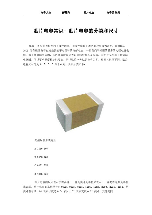
贴片电容常识- 贴片电容的分类和尺寸电容:可分为无极性和有极性两类,无极性电容下述两类封装最为常见,即0805、0603;而有极性电容也就是我们平时所称的电解电容,一般我们平时用的最多的为铝电解电容,由于其电解质为铝,所以其温度稳定性以及精度都不是很高,而贴片元件由于其紧贴电路版,所以要求温度稳定性要高,所以贴片电容以钽电容为多,根据其耐压不同,贴片电容又可分为A、B、C、D 四个系列,具体分类如下:类型封装形式耐压A 3216 10VB 3528 16VC 6032 25VD 7343 35V贴片电容的尺寸表示法有两种,一种是英寸为单位来表示,一种是以毫米为单位来表示,贴片电容的系列型号有0402、0603、0805、1206、1812、2010、2225、2512,是英寸表示法,04 表示长度是0.04 英寸,02 表示宽度0.02 英寸,其他类同型号尺寸(mm)英制尺寸公制尺寸长度及公差宽度及公差厚度及公差0402 1005 1.00±0.05 0.50±0.05 0.50±0.050603 1608 1.60±0.10 0.80±0.10 0.80±0.100805 2012 2.00±0.20 1.25±0.20 0.70±0.201.00±0.201.25±0.201206 3216 3.20±0.30 1.60±0.20 0.70±0.201.00±0.201.25±0.201210 3225 3.20±0.30 2.50±0.30 1.25±0.301.50±0.301808 4520 4.50±0.40 2.00±0.20 ≤2.001812 4532 4.50±0.40 3.20±0.30 ≤2.502225 5763 5.70±0.50 6.30±0.50 ≤2.503035 7690 7.60±0.50 9.00±0.05 ≤3.00贴片电容的命名所包含的参数有贴片电容的尺寸、做这种贴片电容用的材质、要求达到的精度、要求的电压、要求的容量、端头的要求以及包装的要求例风华系列的贴片电容的命名贴片电容的命名:贴片电容的命名所包含的参数有贴片电容的尺寸、做这种贴片电容用的材质、要求达到的精度、要求的电压、要求的容量、端头的要求以及包装的要求。
同容值的电解电容与贴片电容-概述说明以及解释
同容值的电解电容与贴片电容-概述说明以及解释1.引言1.1 概述电解电容和贴片电容都是常见的电子元件之一,广泛应用于电子设备和电路中。
它们在电容值相同的情况下,具有不同的特点和应用场景。
本文将比较同容值的电解电容和贴片电容在性能、优缺点以及使用场景上的差异,并提出对于电容选择的建议。
在电子设备中,电解电容是一种重要的电子元件。
它通过电解液的反应来储存电荷,具有较大的电容值和较高的工作电压。
电解电容具有较高的容量和能量密度,适用于对储能要求较高的电路。
同时,电解电容还具有较低的成本和体积小的特点,使得它在大多数电路中得到广泛应用。
相对而言,贴片电容是一种较新的电子元件,近年来得到了快速发展和广泛应用。
它采用陶瓷材料作为介质,具有较小的体积和较高的精度。
贴片电容在电容值较小、频率较高的电路中有着广泛的应用,例如通信设备、移动设备等。
由于贴片电容可以通过改变陶瓷材料的组合来实现不同的电容值和稳定性,因此在设计灵活性上具有优势。
在本文的后续部分,我们将分别介绍同容值的电解电容和贴片电容的概念和原理,深入探讨它们的特点和应用。
接着,我们将对它们进行性能比较和优缺点分析,以便更好地了解它们之间的区别和选择。
最后,我们将总结同容值的电解电容和贴片电容的特点,并提出对于电容选择的建议。
同时,我们还将展望未来电容技术的发展趋势,以期推动电子元件的进一步发展和应用。
1.2文章结构1.3 目的本文的主要目的是比较并分析同容值的电解电容和贴片电容在电子设备中的应用和特点。
通过深入探讨它们的概念和原理,我们可以更好地了解它们的工作原理和特性。
同时,我们还将对它们的性能进行比较,并分析它们的优点和缺点。
最后,通过对它们在不同使用场景下的比较,我们可以提供一些建议来帮助读者选择适合其需求的电容产品。
通过本文的阅读,读者将能够对同容值的电解电容和贴片电容有一个全面的了解,包括它们的特点、使用场景以及未来的发展趋势。
这对于工程师和技术人员在设计和选择电子设备中的电容时将有很大的帮助。
各种贴片电容容值规格参数表
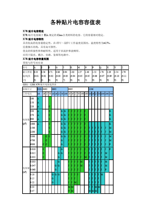
各种贴片电容容值表X7R贴片电容简述X7R贴片电容属于EIA规定的Class 2类材料的电容。
它的容量相对稳定。
X7R贴片电容特性具有较高的电容量稳定性,在-55℃~125℃工作温度范围内,温度特性为±15%。
层叠独石结构,具有高可靠性。
优良的焊接性和和耐焊性,适用于回流炉和波峰焊。
应用于隔直、耦合、旁路、鉴频等电路中。
X7R贴片电容容量范围厚度与符号对应表NPO COG 贴片电容容量规格表默认分类 2009-07-15 16:28 阅读354 评论1字号:大大中中小小NPO(COG)贴片电容属于Class 1温度补偿型电容。
它的容量稳定,几乎不随温度、电压、时间的变化而变化。
尤其适用于高频电子电路。
具有最高的电容量稳定性,在-55℃~125℃工作温度范围内,温度特性为:0±30ppm/℃(COG)、0±60ppm/℃(COH)。
层叠独石结构,具有高可靠性。
优良的焊接性和和耐焊性,适用于回流炉和波峰焊。
应用于各种高频电路,如:振荡、计时电路等。
半导体瓷:其电气性能对外界物理条件极其敏感,可制造各种敏感元件。
比如热敏电阻,气敏电阻。
磁性瓷:即铁氧体瓷,是铁磁性氧化物。
用以制造高频或微波铁氧体器件、以及恒磁器件。
如VCD中的磁珠。
微波介质瓷:其品质因素大,频率特性好,可制作声表面波滤波器(SAWF);陶瓷滤波器(CF)。
贴片电容的材质规格贴片电容目前使用NPO、X7R、Z5U、Y5V等不同的材质规格,不同的规格有不同的用途。
下面我们仅就常用的NPO、X7R、Z5U和Y5V来介绍一下它们的性能和应用以及采购中应注意的订货事项以引起大家的注意。
不同的公司对于上述不同性能的电容器可能有不同的命名方法,这里我们引用的是敝司三巨电子公司的命名方法,其他公司的产品请参照该公司的产品手册。
NPO、X7R、Z5U和Y5V的主要区别是它们的填充介质不同。
在相同的体积下由于填充介质不同所组成的电容器的容量就不同,随之带来的电容器的介质损耗、容量稳定性等也就不同。
贴片电容命名规则及方法
贴片电容命名规则及方法贴片电容的命名:贴片电容的命名所包含的参数有贴片电容的尺寸、做这种贴片电容用的材质、要求达到的精度、要求的电压、要求的容量、端头的要求以及包装的要求例风华系列的贴片电容的命名贴片电容的命名:贴片电容的命名所包含的参数有贴片电容的尺寸、做这种贴片电容用的材质、要求达到的精度、要求的电压、要求的容量、端头的要求以及包装的要求。
一般订购贴片电容需提供的参数要有尺寸的大小、要求的精度、电压的要求、容量值、以及要求的品牌即可。
例风华系列的贴片电容的命名:0805CG102J500NT0805:是指该贴片电容的尺寸套小,是用英寸来表示的08 表示长度是0.08 英寸、05 表示宽度为0.05 英寸CG :是表示做这种电容要求用的材质,这个材质一般适合于做小于10000PF 以下的电容,102 :是指电容容量,前面两位是有效数字、后面的2 表示有多少个零102=10×102 也就是=1000PFJ :是要求电容的容量值达到的误差精度为5%,介质材料和误差精度是配对的500 :是要求电容承受的耐压为50V 同样500 前面两位是有效数字,后面是指有多少个零。
N :是指端头材料,现在一般的端头都是指三层电极(银/铜层)、镍、锡T :是指包装方式,T 表示编带包装,B 表示塑料盒散包装贴片电容的颜色,常规见得多的就是比纸板箱浅一点的黄,和青灰色,这在具体的生产过程中会有产生不同差异贴片电容上面没有印字,这是和他的制作工艺有关(贴片电容是经过高温烧结面成,所以没办法在它的表面印字),而贴片电阻是丝印而成(可以印刷标记)。
贴片电容有中高压贴片电容得普通贴片电容,系列电压有6.3V、10V、16V、25V、50V、100V、200V、500V、1000V、2000V、3000V、4000V贴片电容的尺寸表示法有两种,一种是英寸为单位来表示,一种是以毫米为单位来表示,贴片电容系列的型号有0201、0402、0603、0805、1206、1210、1812、2010、22 25 等。
高压瓷片电容 高压贴片电容
高压瓷片电容高压贴片电容
高压瓷片电容和高压贴片电容是两种不同类型的电容器,它们的主要区别在于使用场合和电介质材料。
高压瓷片电容通常是指以陶瓷材料为电介质,在高压电路中使用的电容器。
由于陶瓷材料的介电常数较高,因此这种电容器具有较高的电容量,通常用于高电压、大容量滤波、储能、隔直等电路中。
而高压贴片电容则是一种表面贴装型电容器,其电介质通常是聚酯、聚丙烯、聚苯乙烯等薄膜材料。
这种电容器的特点是体积小、容量大、稳定性好,并且具有良好的自愈性能,因此广泛应用于各种电子设备中,如电子电源、通信设备、计算机主板等。
总的来说,高压瓷片电容和高压贴片电容都是非常重要的电子元件,它们在电路设计中发挥着重要的作用。
具体使用哪种电容器,需要根据电路的要求和特点来选择。
贴片电解电容的规格

贴片电解电容的规格→贴片电解电容详细规格书选贴片电容就在东莞荣誉电子。
铝电解电容器的工作介质为通过阳极氧化的方式在铝箔表面生成一层极薄的三氧化二铝(Al2O3),此氧化物介质层和电容器的阳极结合成一个完整的体系,两者相互依存,不能彼此独立;我们通常所说的电容器,其电极和电介质是彼此独立的。
电解电容器的阳极铝箔、阴极铝箔通常均为腐蚀铝箔,实际的表面积远远大于其表观表面积,这也是铝质电解电容器通常具有大的电容量的一个原因。
由于采用具有众多微细蚀孔的铝箔,通常需用液态电解质才能更有效地利用其实际电极面积。
贴片电解电容技术:1 影响大型铝电解电容器耐纹波电流能力的因素通常情况下纹波电流Ir为Ir=(1)式中:α为散热系数;Δt为电容芯包温度与环境温度差(温升);A为电容外表面积。
从式(1)中可知,纹波电流Ir与和成正比。
散热系数α,它包括幅射散热和对流散热,它不仅与产品表面的温度差、直径大小、直立或横卧有关,而且与芯包结构、电容器内的导热情况、热流方向、芯包固定方式等密切相关。
由铝电解电容器等效电路可知tanδ=ωCR(2)式中:R为等效串联电阻,它由三部分所组成,即R=R1+R2+R3(3)式中:R1是氧化膜介质损耗所代表的等效串联电阻;R3是极板、导电层的欧姆电阻以及其间的接触电阻;R2是电解质所代表的等效串联电阻,即R2=φ·ρ·d/2s(4)式中:φ为电解纸的渗透系数;ρ为工作电解液的电阻率(Ω·cm);d为电解纸的厚度(cm);s为阳极箔的外观几何尺寸(cm2)。
由以上分析可知,选用氧化膜介质损耗小的铝箔,选择渗透系数小、厚度薄的电解纸,降低工作电解液的电阻率和粘度,改进产品结构等都可明显降低产品的tanδ。
通过降低tanδ,增大产品的散热系数,都可提高产品耐纹波电流的能力,从而保证产品达到寿命长等要求。
2 变频器对大型铝电解电容器的技术要求变频器的简单工作原理图如图1所示。
1206贴片电容最大容值和耐压
1206贴片电容是一种常见的电子元件,用于电路中的滤波、耦合、终端匹配等功能。
在电子设备中,为了保证电路的稳定性和可靠性,选择合适的电容器至关重要。
在选择1206贴片电容时,最大容值和耐压是两个重要的参考指标。
本文将就1206贴片电容的最大容值和耐压进行详细介绍和分析。
一、1206贴片电容的最大容值1206贴片电容的最大容值是指该型号电容器所能容纳的最大电荷量。
在实际应用中,通常会根据具体的电路需求来选择合适的最大容值。
以下是影响1206贴片电容最大容值的主要因素:1. 电路需求:不同的电路对电容容值的要求有所不同。
一般来说,需要大电流通过的电路需要容值较大的电容器。
2. 工作频率:1206贴片电容的最大容值还受到工作频率的影响。
在高频电路中,需要选择容值较小的电容器来确保性能稳定。
3. 电压水平:1206贴片电容的最大容值也与电压水平相关。
在高压电路中,需要选择承受高电压的大容值电容器。
根据以上因素,选择1206贴片电容的最大容值时,需要综合考虑电路需求、工作频率和电压水平,以确保电容器能够有效地满足电路的需求。
二、1206贴片电容的耐压1206贴片电容的耐压是指电容器能够承受的最大电压。
在电子设备中,耐压是一个非常重要的指标,直接关系到电路的安全可靠运行。
以下是影响1206贴片电容耐压的主要因素:1. 化学材料:1206贴片电容的材料不同,在耐压方面的性能也有所差异。
一般来说,有机电解质电容器的耐压较低,而钽质电解质电容器的耐压较高。
2. 结构设计:电容器的内部结构设计也会影响其耐压能力。
合理的结构设计能够有效提高电容器的耐压性能。
3. 工艺水平:生产工艺水平直接影响了电容器的品质,对于耐压来说尤为重要。
优质的工艺能够确保电容器的耐压性能稳定可靠。
在选择1206贴片电容时,需要根据具体电路需求和工作环境来确定合适的耐压水平,以确保电容器能够安全稳定地工作。
总结:1206贴片电容的最大容值和耐压是选择该型号电容器时需要重点考虑的指标,合理选择最大容值和耐压能够有效地满足电路需求,确保电子设备的稳定性和可靠性。
常用高压贴片和大容量贴片电容规格

常用高压贴片和大容量贴片电容规格LED灯常用高压贴片和大容量贴片电容规格高压陶瓷贴片电容-可代替传统插件电容缩小电源体积(LED电源专用) 规格主要有:102/1KV 1206封装222/1KV 1206封装472/1KV 1206封装103/1KV 1206封装2.2u/100V 1812封装473/250V 1206封装473/630V 1206封装10u/16V 1206封装10u/25V 1210封装22u/10V 1206封装22U/16V 1210封装以上都为X7R或X5R材质,容量精度为10%LED阻容降压用-(代替插件CBB)250V 224 1812封装250V 334 1812封装250V 474 1812封装250V 684 1812封装250V 105 1812封装500V 224 1812封装400V 105 2220封装以上都为X7R材质,耐125度高温无极灯我司专业生产高压高频贴片电容-高频无极灯专用(代替CBB) 规格主要有:1KV NP0 101 221 331 471 102。
100P 3KV NP0 1808/1812封装220P 3KV NP0 1808或1812封装-820P 2KV NP0 1812封装102 2KV NP0 1812封装100P 1KV NP0 1206封装220P 1KV NP0 1206封装470P 1KV NP0 1206封装102 1KV NP0 1206封装0.47u 100V X7R 1206封装0.68u 100V X7R 1206封装节能灯高压贴片电容-代替插件瓷片和薄膜电容缩小体积(节能灯专用) 规格主要有:223/100V 1206封装102/1KV 1206封装332/1KV 1206封装222/1KV 1206封装250V/473 1206封装400V/104 1210封装HID灯常用高压贴片电容和大容量贴片电容规格如下:1KV 100p 1206封装1KV 221 1206封装1KV 102 1206封装1KV 222 1206封装1KV 472 1206封装1KV 103 1206封装630V 104 1812封装10U/25V 1210封装10U/50V 1210封装以上都为陶瓷X7R材质,耐温-55-125度。
贴片叠层瓷介电容器(SMD贴片电容)详细介绍
北京芯联科泰电子有限公司贴片叠层瓷介电容器(SMD贴片电容)详细介绍:贴片电容全称:多层(积层,叠层)片式陶瓷电容器,也称为贴片电容,片容。
英文缩写:MLCC。
基本概述贴片电容(多层片式陶瓷电容器)是目前用量比较大的常用元件,就AVX公司生产的贴片电容来讲有NPO、X7R、Z5U、Y5V等不同的规格,不同的规格有不同的用途。
下面我们仅就常用的NPO、X7R、Z5U和Y5V来介绍一下它们的性能和应用以及采购中应注意的订货事项以引起大家的注意。
不同的公司对于上述不同性能的电容器可能有不同的命名方法,这里我们引用的是AVX公司的命名方法,其他公司的产品请参照该公司的产品手册尺寸贴片电容的尺寸表示法有两种,一种是英寸为单位来表示,一种是以毫米为单位来表示,贴片电容的系列型号有0402、0603、0805、1206、1210、1808、1812、2010、2225、2512,是英寸表示法, 04 表示长度是0.04 英寸,02 表示宽度0.02 英寸,其他类同型号尺寸(mm)英制尺寸公制尺寸长度及公差宽度及公差厚度及公差0402 1005 1.00±0.05 0.50±0.05 0.50±0.050603 1608 1.60±0.10 0.80±0.10 0.80±0.100805 2012 2.00±0.20 1.25±0.20 0.70±0.20 1.00±0.20 1.25±0.201206 3216 3.00±0.30 1.60±0.20 0.70±0.20 1.00±0.20 1.25±0.201210 3225 3.00±0.30 2.54±0.30 1.25±0.30 1.50±0.301808 4520 4.50±0.40 2.00±0.20 ≤2.001812 4532 4.50±0.40 3.20±0.30 ≤2.502225 5763 5.70±0.50 6.30±0.50 ≤2.503035 7690 7.60±0.50 9.00±0.05 ≤3.00命名贴片电容的命名所包含的参数有贴片电容的尺寸、做这种贴片电容用的材质、要求达到的精度、要求的电压、要求的容量、端头的要求以及包装的要求。
风华中高压贴片电容规格书
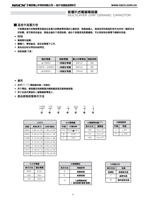
MULTILAYER CHIP CERAMIC CAPACITOR(:)DC Medium-voltage MLCCDC medium-voltage MLCC has good high-voltage reliability,it is made in special design that based on the MLCC technology and equipments.It is suitable for surface-mounting ,can improve the properties of circuits.New monolithic structureThe size of the capacitor is small,yet has high electrostatic capacitance,can operate at high-voltage levels.Has good solderability.Technology Parameter (refer to the picture below):DC-DC converter.The circuit filter and vibration bell of telephone,electrograph and modem.Snubber circuit for switching power supply.FeaturesApplicationsProduct Part Number Expression1206CG100J202NTWMULTILAYER CHIP CERAMIC CAPACITORCapacitance RangeOutside DimensionWMULTILAYER CHIP CERAMIC CAPACITORMULTILAYER CHIP CERAMIC CAPACITORMULTILAYER CHIP CERAMIC CAPACITOR【 南京南山半导体有限公司 — 贴片电容选型资料】MULTILAYER CHIP CERAMIC CAPACITORX7R 1808 (V)10018122225200 200 200 5001000 2000 3000 4000 100 500 1000 2000 3000 4000 100 500 1000 2000 3000 4000 5000 /250 /250 /250100PF 150PF 330PF 470PF 680PF 1000PF 1nF 2.2nF 3.3nF 4.7nF 6.8nF 10nF 12nF 15nF 22nF 27nF 33nF 39nF 47nF 56nF 68nF 100nF 120nF 150nF 220nF 270nF 330nF 470nF 680nF 1 F 2.2 F 3.3 F 10 F 22 F75【 南京南山半导体有限公司 — 贴片电容选型资料】ItemX7R Medium-voltage MLCCDielectric 1808 1812 2225 Size Rated 100 200 5001000 2000 3000 4000 100 200 500 1000 2000 3000 4000 100 200 500 1000 2000 3000 4000 5000 /250 /250 Volatage(V) /250 Capacitance 100PF 150PF 330PF 470PF 680PF 1000PF 1nF 2.2nF 3.3nF 4.7nF 6.8nF 10nF 12nF 15nF 22nF 27nF 33nF 39nF 47nF 56nF 68nF 100nF 120nF 150nF 220nF 270nF 330nF 470nF 680nF 1 F 2.2 F 3.3. F 10 F 22 F76【 南京南山半导体有限公司 — 贴片电容选型资料】MULTILAYER CHIP CERAMIC CAPACITORY5V 0603 (V) 100 100 0805 200 250 100 1206 200 250 100 1210 200 250 100 1812 200 250 100 2225 200 2501000PF 1.5nF 2.2nF 3.3nF 4.7nF 6.8nF 10nF 12nF 15nF 22nF 27nF 33nF 39nF 47nF 56nF 68nF 100nF 150nF 220nF 270nF 330nF 390nF 470nF 680nF 820nF 1 F 2.2 3.3 10 F F F77【 南京南山半导体有限公司 — 贴片电容选型资料】ItemY5V Medium-voltage MLCC 1210 100 200 250 100 1812 200 250 100 2225 200 250Dielectric 0603 0508 1206 Size Rated Volatage(V) 100 100 200 250 100 200 250 Capacitance 1000PF 1.5nF 2.2nF 3.3nF 4.7nF 6.8nF 10nF 12nF 15nF 22nF 27nF 33nF 39nF 47nF 56nF 68nF 100nF 150nF 220nF 270nF 330nF 390nF 470nF 680nF 820nF 1 2.2 3.3 10 F F F F78【 南京南山半导体有限公司 — 贴片电容选型资料】MULTILAYER CHIP CERAMIC CAPACITORCOG1-551251. 2. 3. 2 4. , , , , , 105.3 4 :HP4278A 1. 2. 5 (D.F.) 3. HP4284 25 5 :30% 75% 1.0 0.2V C<1000PF,1.0 0.1MHz; C 1000PF,1.0 0.1KHZ :10( :SF2511) >500V6I.R. 500V: , 60 5>1 5 7 >1 2 >1 21000V 1000V 2000V 2000V50mA 50mA 10mA 150+0/-10 60 55S 5S 5S824 2 -55 125 25975235 5 5 2 0.5 150+0/-10 5% 0.5PF, 10 1 D.F. 24 2 265 5 24 2 25 2.5mm/ : 25 2.5mm/ 60 524510I.R.1 2100 170120 2001 179【 南京南山半导体有限公司 — 贴片电容选型资料】Middle and high Voltage COG MLCC reliability test methodNumber 1 Item Operating Temperature Range Appearance -55 Standard 125 Test Method21.Good ceramic body color continuity. 2.The chips have no visual damages and must be very smooth. 3.No exposed innerelectrode, no cracks or holes. 4.The outer electrode should have no cracks, holes, damages or surface oxidation. 5.Outer electrode no prolongation or the prolongation is less than half of that of the termination width. Within the specified dimensions Within the specified toleranceCr 5PF 0.56% -4 5PF Cr 50PF 1.5[(150/Cr)+7] 10 Cr 50PF 0.15%Check by using microscope10.3 4Dimensions Capacitance Dissipation Factor (DF) Insulation ResistanceUsing micrometer or vernier calipers Measuring Equipment:HP4278 capacitance meter,HP4284 capacitance, Measuring Conditions: 1.Measuring Temperature:25 5 .Humidity: 30%~75%. 2.Measuring Voltage:1.0 0.2V. 3.Measuring Frequency:C<1000PF 1.0 0.1MHz C 1000PF 1.0 0.1KHz Measuring Equipment:Insulation resistance meter (such as Sf2511 insulation resistance). Measuring Method:Must measure at rated voltage, and if Ur>500V,then just use 500V,measure the IR within 60 1 seconds. Ur Max. Current Measuring Time 1000V 1000V 2000V 2000V 50mA 50mA 10mA 5S 5S 5S56C<10nF,IR 5 10 C>10nF,IR CR 500S10Withstanding Voltage 7Requirement >1.5Ur >1.2Ur >1.2Ur8Must meet the capacitor Capacitance temperature coefficient Temperature requirements within the Characteristics operating temperature range. Solderability Tin coverage 75% should be of the outer electrode covered by Tin Appearance Cap. Change ratio No defects visible 5% or 0.5PF whichever is bigger Same as original standard Same as original standardFirst, pre-heat: heat treat 60 5 minutes at 150+0/-10 , then set it for 24 2 hours at room temperature. Measure the capacitance at 55~125 or 55~85 , the capacitance change ratio comparing to that of 25 must be within the specified range. Dip the capacitor into ethanol or colophony solution, and then dip it into 235 5 eutectic solder solution for 2 0.5 seconds. Dipping speed: 25 2.5mm/second. First pre-heat: heat treat for 60 5 minutes at 150+0/-10 , then set it for 24 2 hours at room temperature. Then pre-heat the capacitance according to the following chart. Dip the capacitor into 265 5 eutectic solder solution for 10 1 seconds. Then set it for 24 2 hours at room temperature, then measure. Dipping speed: 25 2.5mm/second. Preheat conditions: Stage Temperature Time 1 2 100 170 120 200 1minutes 1minutes9 Resistance to Soldering10DFIR80【 南京南山半导体有限公司 — 贴片电容选型资料】MULTILAYER CHIP CERAMIC CAPACITOR1 10N11 10N,10 1 :1.0mm/ 11.5mm 10 D.F. 12 55Hz10 55Hz 10Hz 2 6 123 420 mmmm3mm mm mm mmmm150+0/-10 14 24 260 524 281【 南京南山半导体有限公司 — 贴片电容选型资料】NumberItem Adhesive Strength of TerminationStandard No removal of the termination or other defect shall occurTest Method Solder the capacitor to the test jig (glass epoxy resin board) shown in Fig.1 using a eutectic solder.Then apply a 10N force inthe direction shown as the arrowhead.The soldering shall be done either with an iron or using the reflow method and shall be conducted with care so that the soldering is uniform and free of defects such as heat shock,etc.11Fig.1 Vibration Resistance10N,10 1s Speed:1.0mm/s Glss epoxy resin board12Appearance No defects or Solder the capacitor to the test jig (glass epoxy resin abnormities board). The capacitor should be subjected to a simple harmonic motion having a total amplitude of 1.5mm, the Capacitance Within the frequency being varied uniformly between the specified approximate limits of 10 and 55Hz, shall be traversed tolerance range (from 10 Hz to 55 Hz then 10 Hz again) in approximately 1 minute.This motion shall be applied for a period of 2 DF Same as hours in each 3 mutually perpendicular directions original (total is 6 hours). standardFig.2 Bending Resistance No cracks or other defects shall occur Solder the capacitor to the test jig (glass epoxy resin board) shown in Fig.3 using a eutectic solder. Then apply a force in the direction shown in Fig.4. The soldering shall be done either with an iron or using the reflow method and shall be conducted with care so that the soldering is uniform and free of defects such as heat shock, etc. mmmm13mmmm mmmmTemperature Cycle 14Appearance No defects or abnormitiesPre-treatment: Heat-treat the capacitor for 60 5 minutes at 150+0/-10 , then set it for 24 2 hours at room temperature. Perform five cycles according to the four heat treatments listed in the following table. Set it for 24 2 hours at room temperature, the measure.82【 南京南山半导体有限公司 — 贴片电容选型资料】MULTILAYER CHIP CERAMIC CAPACITOR2.5% 0.25PF, min. 14 D.F. I.R. 10000M 1 2 3 4 2 3 30 2 30 2 3 3 3 34029095 24 2500+24/-05% 0.5PF, 15 ( ) D.F. I.R. 10000M1.5 50mA ( 5% 0.5PF, 16 .) >2000V100012 24 21.2D.F. I.R. 10000M83【 南京南山半导体有限公司 — 贴片电容选型资料】NumberItems Temperature CycleStandard Cap. Change ratio 2.5% or 0.25PF whichever is larger Same as original standard More than 10000M Heat-treatment:Test MethodD.F. 14 I.R.Stage Temperature Time 1 lowest operating temperature 3 30 2 2 Room Temperature 3 Highes operating temperature 2 30 4 Room Temperature 2min. 3 3 3 3Humidity Steady State 15AppearanceNo defects or abnormities 5% or 0.5PF whichever is larger Same as original standard More than 10000M No defects or abnormities 5% or 0.5PF (whichever is larger) Same as original standard More than 10000MSet the capacitor for 500+24/-0 hours at the condition of 40 2 and 90-95% humidity. Then remove and set it for 24 2 hours at room temperature, then measure.Cap. Change ratioD.F.I.R. Life Test AppearanceCap. Change ratio 16Apply 1.5 times rated voltage to the capacitor for 1000 12 hours at the upper temperature limits, the charging current should be less than 50mA. Remove and set it for 24 2 hours at room temperature, then measure.(If Ur>2000V,apply 1.2times Ur to test)D.F.I.R.84【 南京南山半导体有限公司 — 贴片电容选型资料】MULTILAYER CHIP CERAMIC CAPACITORX7R1-551251. 2. 3. 2 4. , , , , , 105.3 4 : HP4278A HP42845(D.F.)25010-41.255:30% 75% 2. 3. : :1.0 :1.0 0.2V 0.1KHz ( :SF2511 ) >500V , 60 56I.R.C 25nF,IR 10000M C>25nF,R C 500S 500V:>1 5 7 >1 2 >1 21000V 1000V 2000V 2000V50mA 50mA 10mA5S 5S 5S150+0/-10 24 8 25 -55 125 2605235 9 75 245 5 25 2.5mm/ 2 0.5585【 南京南山半导体有限公司 — 贴片电容选型资料】General X7R MLCC reliability test methodNumber 1 Item Operating Temperature Range Appearance -55 Standard 125 Test Method21.Good ceramic body color continuity. 2.The chips have no visualdamages and must be very smooth. 3.No exposed inner- electrode, no cracks or holes. 4.The outer electrode should have no cracks, holes, damages or surface oxidation. 5.Outer electrode no prolongation or the prolongation is less than half of the termination width. Within the specified dimensions Within the specified tolerance 250 10-4Check by using microscope10 .3 4Dimensions Capacitance Dissipation Factor (DF)5Using micrometer or vernier calipers Measuring Equipments: HP4278 capacitance meter, HP4284 capacitance, Measuring Conditions: 1.Measuring Temperature: 25 5 . Humidity: 30% 75%. 2.Measuring Voltage: 1.0 0.2V. 3.Measuring Frequency:1.0 0.1KHz Measuring Equipment: Insulation resistance meter (such as Sf2511 insulation resistance). Measuring Method: Must measure at rated voltage, and measure the IR within 60 1 seconds. Ur 1000V 1000V 2000V Max. Current Measuring Time 50mA 50mA 10mA 5S 5S 5SInsulation Resistance 6C 25nF,IR 10000M C>25nF,R C 500SWithstanding Voltage 7Requirement >1.5Ur >1.2Ur >1.2Ur2000V8Capacitance Temperature CharacteristicsMust meet the capacitor character temperature coefficient requirements within the operating temperature range. 75% of the outer electrode should be covered by TinFirst, pre-heat: heat treat 60 5 minutes at 150+0/-10 ,then set it for 24 2 hours at room temperature. Measure the capacitance at -55 125 ,the capacitance change ratio comparing to that of 25 must be within the specified range. Dip the capacitor into ethanol or colophony solution,and then dip it into 245 5 eutectic solder solution for 2 0.5 seconds. Dipping speed:25 2.5mm/second.Solderability 986【 南京南山半导体有限公司 — 贴片电容选型资料】MULTILAYER CHIP CERAMIC CAPACITOR150+0/-10 10% D.F. 10 I.R. 25 : 10 1 24 2 26560 5 24522.5mm/1 2100 170120 2001 1110N11 10N,10 1 :1.0mm/ 11.5mm 10 D.F. 55Hz 55Hz 10Hz 1 2 12 6 1023 13 ( ) 487【 南京南山半导体有限公司 — 贴片电容选型资料】NumberItemStandardTest Method First pre-heat: heat treat for 60 5 minutes at 150+0/-10 , then set it for 24 2 hours at room temperature. Then pre-heat the capacitance according to the following chart. Dip the capacitor into 265 5 eutectic solder solution for 10 1s. Then set it for 24 2 hours at room temperature, then measure. Dipping speed: 25 2.5mm/second. Preheat conditions: Stage Temperature Time 1 2 100 170 120 200 1minute 1minuteResistance to Appearance No defects visible Soldering Cap. Change Within 10% ratio DF 10 IR Same as original spec. Same as original spec.Adhesive Strength of TerminationNo removal of the terminations or other defect shall occur11Solder the capacitor to the test jig (glass epoxy resin board) shown in Fig.1 using a eutectic solder. Then apply a 10N force in the direction shown as the arrowhead. The soldering shall be done either with an iron or using the reflow method and shall be conducted with care so that the soldering is uniform and free of defects such as heat shock, etc. 10N,10 1s Speed:1.0mm/s Glss epoxy resinboardFig.1 Resistance to Soldering Appearance No defects visible or abnormities Capacitance Within the specified tolerance range D.F. 12 Same as original spec.Solder the capacitor to the test jig (glass epoxy resin board). The capacitor should be subjected to a simple harmonic motion having a total amplitude of 1.5mm, the frequency being varied uniformly between the approximate limits of 10 and 55Hz, shall be traversed (from 10 Hz to 55 Hz then 10 Hz again) in approximately 1 minute. This motion shall be applied for a period of 2 hours in each 3 mutually perpendicular directions (total is 6 hours).Fig.2 Bending Resistance No cracks or other defects shall occur Solder the capacitor to the test jig (glass epoxy resin board) shown in Fig.3 using a eutectic solder. Then apply a force in the direction shown as Fig.4. The soldering shall be done either with an iron or using the reflow method and shall be conducted with care so that the soldering is uniform and free of defects such as heat shock, etc.1388【 南京南山半导体有限公司 — 贴片电容选型资料】MULTILAYER CHIP CERAMIC CAPACITOR20 mmmmmm13mmmmmmmmmin. 20% 1 2 14 D.F. I.R. 3 4 2 3 30 2 30 2 3 3 3 340 20% 15 ( ) D.F. I.R.29095 48 2500+24/-01.5 20% .) 16 D.F. I.R 50mA ( >2000V100012 24 21.289【 南京南山半导体有限公司 — 贴片电容选型资料】NumberItem Bending ResistanceStandardTest Methodmmmmmm13mm mmmmTemperature CycleAppearanceNo defects or abnormities 20%Cap. Change Within ratio 14Stage Temperature Time min. 1 Min. Operating Temperature 3 30 3 2 Room Temperature 2 3 3 Max. Operating Temperature 2 30 3 4 Room Temperature 2 3D.F.Same as original Specification Same as original Specification No defects or abnormities 20% Set the capacitor for 500+24/-0 hours at the condition of 40 2 and 90-95% humidity. Then remove and set it for 48 2 hours at room temperature, then measure.I.R.Humidity Steady StateAppearanceCap. Change within ratio D.F.15 I.R. Life Test AppearanceSame as original Specification Same as original Specification No defects or abnonrmities 20% Apply 1.5 times rated voltage to the capacitor for 1000 12 hours at the upper temperature limits, the charging current should be less than 50mA. Remove and set it for 24 2 hours at room temperature, then measure.(If Ur>2000V,apply 1.2Ur to test.)Cap. Change within ratio 16 D.F.Same as original specification Same as original specificationI.R.90【 南京南山半导体有限公司 — 贴片电容选型资料】MULTILAYER CHIP CERAMIC CAPACITORY5V1-25~851. 2. 3. 2 4. 5. , , , , ,103 4 : HP4278A 1. 5 (D.F.) 500 10-4HP4284 25 5 75% 0.2V 0.1kHz:30% 2. 3. : :1.0 :1.06I.R.C 25nF,IR 40000M C>25nF,R C 500S( : ,: SF2511 60 5)7>300V >400V >500V100V 200V 250V50mA 50mA 50mA5S 5S 5S150+0/-10 8 24 -25 85 2605 25975235 25 0.52455 25 2.5mm/91【 南京南山半导体有限公司 — 贴片电容选型资料】General Y5V MLCC reliability test methodNumber 1 Item Operating Temperature Range Appearance -25 85 Standard Test Method21.Good ceramic body color continuity. 2.The chips have no visualdamages and must be very smooth. 3.No exposed inner- electrode, no cracks or holes. 4.The outer electrode should have no cracks, holes, damages or surface oxidation. 5.Outer electrode no prolongation or the prolongation is less than half of that of the termination width. Within the specified dimensions Within the specified tolerance 500 10-4Check by using microscope10.3 4Dimensions Capacitance) Dissipation Factor (DF)Using micrometer or vernier calipers Measuring Equipments: HP4278 capacitance meter, HP4284 capacitance, Measuring Conditions: 1.Measuring Temperature: 25 5 . Humidity: 30% 75%. 2.Measuring Voltage: 1.0 0.2V. 3.Measuring Frequency: 1.0 0.1KHz Measuring Equipment: Insulation resistance meter (such as Sf2511 insulation resistance). Measuring Method: Must measure at rated voltage, and measure the IR within 60 5seconds. Ur 1000V 1000V 2000V Max. Current Measuring Time 50mA 50mA 10mA 5S 5S 5S5Insulation Resistance 6C 25nF,IR 40000M C>25nF,R C 500SWithstanding Voltage 7Requirement >1.5Ur >1.2Ur >1.2Ur2000VCapacitance Temperature Characteristics 8Must meet the capacitor temperature coefficient requirements within the operating temperature range.First, pre-heat: heat treat 60 5 minutes at 150+0/-10 , then set it for 24 2 hours at room temperature. Measure the capacitance at 55 125 or 55 85 ,the capacitance change ratio comparing to that of 25 must be within the specified range. Dip the capacitor into ethanol or colophony solution,and then dip it into 235 5 (or 245 5 leadless eutectic solder solution) eutectic solder solution hanging lead for 2 0.5seconds. Dipping speed: 25 2.5mm/second.Solderability 975% of the outer electrode should be covered by Tin92【 南京南山半导体有限公司 — 贴片电容选型资料】MULTILAYER CHIP CERAMIC CAPACITOR150+0/-10 30% D.F. I.R. 10 60 5 24 22655 24 2 25 2.5mm/ :1011 2100 170120 200 11 110N11 10N,10 1 :1.0mm/ 11.5mm D.F. 10 55Hz 12 55Hz 10Hz 1 2 6 1023 ( 13 ) 493【 南京南山半导体有限公司 — 贴片电容选型资料】NumberItemStandardTest Method First pre-heat: heat treat for 60 5 minutes at 150+0/-10 , then set it for 24 2 hours at room temperature. Then pre-heat the capacitance according to the following chart. Dip the capacitor into 265 5 eutectic solder solution for 10 1s. Then set it for 24 2 hours at room temperature, then measure. Dipping speed: 25 2.5mm/second. Preheat conditions: Stage Temperature Time 1 2 100 170 120 200 1minute 1minuteResistance to Appearance No defects visible Soldering Cap. Change Z5U, Y5V: within ratio DF 10 IR30%Same as original spec. Same as original spec.Adhesive Strength of TerminationNo removal of the terminations or other defects shall occur11Solder the capacitor to the test jig (glass epoxy resin board) shown in Fig.1 using a eutectic solder. Then apply a 10N force in the direction shown as the arrowhead. The soldering shall be done either with an iron or using the reflow method and shall be conducted with care so that the soldering is uniform and free of defects such as heat shock, etc. 10N,10 1s Speed:1.0mm/s Glss epoxy resinboardFig.1 Resistance to Soldering Appearance No defects visible or abnormities Capacitance Within the specified tolerance range D.F. 12 Same as original spec.Solder the capacitor to the test jig (glass epoxy resin board). The capacitor should be subjected to a simple harmonic motion having a total amplitude of 1.5mm, the frequency being varied uniformly between the approximate limits of 10 and 55Hz, shall be traversed (from 10 Hz to 55 Hz then 10 Hz again) in approximately 1 minute. This motion shall be applied for a period of 2 hours in each 3 mutually perpendicular directions (total is 6 hours).Fig.2 Bending Resistance No cracks or other defects shall occur Solder the capacitor to the test jig (glass epoxy resin board) shown in Fig.3 using a eutectic solder. Then apply a force in the direction shown as Fig.4. The soldering shall be done either with an iron or using the reflow method and shall be conducted with care so that the soldering is uniform and free of defects such as heat shock, etc.1394【 南京南山半导体有限公司 — 贴片电容选型资料】MULTILAYER CHIP CERAMIC CAPACITOR20 mm mmmm13mm mmmmmm30%min. 1 2 3 4 3 2 30 2 30 2 3 3 3 3D.F. 14 I.R.40 30%29095 48 2500+24/-015()D.F. I.R.30% 16 D.F. I.R 48 21.5 50mA10001295【 南京南山半导体有限公司 — 贴片电容选型资料】NumberItem Bending ResistanceStandardTest Methodmmmm13mmmmmmmmTemperature CycleAppearanceNo defects or abnonrmities 2.5Cap. Change Within ratio 14Stage Temperature Time 30 1 Min. Operating Temperature 3 2 Room Temperature 2 3 Max. Operating Temperature 2 30 4 Room Temperature 2min. 3 3 3 3D.F.Same as original spec. Same as original spec. No defects or abnonrmities Set the capacitor for 500+24/-0 hours at the condition of 40 2 and 90-95% humidity. Then remove and set it for 24 2 hours at room temperature, then measure.I.R.Humidity Steady State 15AppearanceCap. Change within 30% ratio Same as D.F. original spec. I.R. Same as original spec. No defects or abnonrmities 30%Life TestAppearanceCap. Change within ratio 16 D.F.Same as original spec. Same as original spec.Apply 1.5 times rated voltage to the capacitor for 1000 12 hours at the upper temperature limits, the charging current should be less than 50mA. Remove and set it for 24 2 hours at room temperature, then measure.I.R.96。
超高压瓷片电容
超高压瓷片电容是一种特殊类型的电容器,其介质为陶瓷材料。
这种电容器的主要特点是具有极高的耐压能力,常见的电压规格有2kv和3kv。
此外,超高压瓷片电容还具有体积小、频率特性好、耐磨损直流高压等特点。
在应用中,超高压瓷片电容主要用于高压旁路和耦合电路中,特别适用于电视接收机和扫描等电路中。
此外,在LED灯行业中,超高压陶瓷电容也有广泛的应用,主要用于消除高频干扰和提供稳定的直流电压。
随着材料、电极和制造技术的进步,超高压陶瓷电容器的发展取得了长足的进展,已成为大功率高压电子产品不可缺少的元件之一。
请注意,虽然超高压瓷片电容具有许多优点,但在使用过程中仍需注意安全和规范操作,避免因操作不当而导致损坏或安全事故的发生。
贴片高压陶瓷电容材料安全资料表MSDS

材料安全资料表MATERIAL SAFETY DATA SHEET1、产品及公司证明产品名称:贴片高压陶瓷电容类似:X7R、C0G化学式:无产品名称:贴片电容供应商名称:紧急联络方式:原料信息组成原料CAS数字百分比BaTio3 Cu Ni Sn 12047-27-77440-50-87440-02-07440-31-595% 、3%1%1%2.危险性鉴别紧急概况:NA不利人体健康因素:NA环境因素:NA物质及化学危险:NA具体危险:NA3.急救测验吸入物:NA吞食:需联系医生医治皮肤接触:用清水冲洗眼睛接触:用清水冲洗保护急救人员:医生笔记口述:4.测验消防工作扑灭传播:NA火焰及爆炸危险:NA特殊消防程序:NA保护消防人员的特殊设备:NA测验免除意外个人预防措施:NA环境预防措施:NA去污程序:NA5.移动与储存轻装轻卸,防止包装损坏,不应与潮湿物品混合堆置,放在通风干燥处。
6.宣传管制/个人防护估计工程:NA管理因素:NA价值标准范围:NA生物学标准:NA个人防护装备:手套呼吸保护:NA手防护:测试电压及接触产品时戴白纱手套或绝缘手套眼睛防护:NA皮肤与身体防护:NA7物质与化学性质静止物质:固体表格/格式颜色: 浅黄色/浅褐色气味:无臭酸碱值: 中性沸点:NA分解温度:约1200℃内燃点和使用方法:N A自然温度:NA 爆炸性质:NA最大爆炸压力:NA 蒸汽密度:NA密度:NA 溶解性:NA8、稳定性与活动性稳定性:在正常温湿度及压力范围内其稳定性好具体情况下可能发生危险的反应:NA预防情形:NA预防材料:强酸与强碱分解危险的产品:NA9、毒物资料严重毒性:NA局部效果:NA过敏化作用:NA慢性或长期毒性:NA具体结果:NA10、生态通知不影响生态环境11、清除原因清除方法以安全和环境优先:参照相关法规进行处理、回收使用12、运输资料国际管制:NAUN级别数字:NA运输具体的预防考验和状态:NA13、管理资料NA14、其它资料NFPA Ratings: NALabcl Hazard Warning: NALiterature References: NA。
交流高压贴片电容

交流高压贴片电容
高压贴片电容是一种常见的电子元件,广泛应用于各种电路中。
它具有体积小、容量大、电压高、频率响应好等优点,因此在电子设备中扮演着重要的角色。
高压贴片电容的特点之一是体积小。
相比于传统的电容器,高压贴片电容的体积要小得多。
这使得它可以在空间有限的电路板上得到灵活的布局,为电路设计师提供了更多的选择空间。
即使在体积受限的情况下,高压贴片电容也能够提供足够的电容量,以满足电路的需求。
高压贴片电容还具有较高的工作电压。
相比较于传统的电容器,高压贴片电容可以承受更高的电压,从而满足一些特殊电路的需求。
它的高电压特性使得它在一些高压应用中非常有用,如电源电路、高压放大电路等。
高压贴片电容还具有良好的频率响应。
在高频电路中,传统的电容器往往会因为其自身的电感效应而导致频率响应的下降。
而高压贴片电容则不会受到这样的影响,它能够提供更好的频率响应,从而保证电路的稳定性和性能。
值得一提的是,虽然高压贴片电容有很多优点,但也存在一些挑战。
例如,由于其体积小,高压贴片电容在制造过程中更加复杂,容易受到环境因素的影响。
此外,高压贴片电容的价格相对较高,这也
限制了它在某些应用中的使用。
高压贴片电容是一种在电子领域中非常重要的元件。
它的体积小、容量大、电压高、频率响应好等特点使得它在各种电路中得到广泛应用。
随着科技的不断发展,相信高压贴片电容将会在更多的领域中发挥重要作用,为人们的生活带来更多便利。
- 1、下载文档前请自行甄别文档内容的完整性,平台不提供额外的编辑、内容补充、找答案等附加服务。
- 2、"仅部分预览"的文档,不可在线预览部分如存在完整性等问题,可反馈申请退款(可完整预览的文档不适用该条件!)。
- 3、如文档侵犯您的权益,请联系客服反馈,我们会尽快为您处理(人工客服工作时间:9:00-18:30)。
★ ·单片结构保证有极佳的机械性强度及可靠性
★ ·极高的精确度,在进行自动装配时有高度的准确性
★ ·因仅有陶瓷和金属构成,故即便在高温,低温环境下亦无渐衰的现象出现,具有较强可靠性与稳定性
★ ·低集散电容的特性可完成接近理论值的电路设计
模块电源 常用大容量贴片电容和高压贴片电容
100V 1U 1812封装
100V 2.2U 1812封装
50V 4.7U 1812封装
25V 10U 1812封装
25V 22U 1812封装
10V 47U 1812封装
6.3V 100U 1812封装
50V 10U 2220封装
1KV NP0 101 221 331 471 102。。1206尺寸
3KV 100P NP0 1808/1812尺寸
3KV 22I NP0 1808或1812尺寸
3KV 471 NP0 1812尺寸
2KV 821 NP0 1812尺寸
2KV 102 NP0 1812尺寸
100V 474 X7R 1206尺寸
QQ:381156356 古珍男
大功率路灯电源专用TDK陶瓷贴片电容
缩小产品体积提高产品寿命。
C4532X7R2A225KT-1812 100V 2.2UF+-10%
C4532X7R2E105KT-1812 250V 1UF+-10%
我司专业生产高压高频贴片电容-高频无极灯专用(代替CBB) 耐压;125度。
★ ·残留诱导系数小,确保上佳的频率特性
★ ·因电解电容器领域也获得了电容,故使用寿命延长,更造于具有高可靠性的电源
★ ·由于ESR低,频率特性良好,故最适合于高频,高密度类型的电源
LED阻容降压用高压贴片电容(代替插件CBB)
250V 224 1812封装
250V 334 1812封装
主要规格有:
1206 333/630V
1210 333/1KV
1206 473/400V或450V或 630V-
1210 104/400V或500V或630V
1210 224/400V或450V 以上都为X7R或TDK X7T材质 精度K
类安规贴片电容
安规贴片电容代替插件瓷片安规,或Y1
LED灯常用高压贴片和大容量贴片电容
高压陶瓷贴片电容-可代替传统插件电容缩小电源体积(LED电源专用)
规格主要有:
100v/2.2u 1812封装(大功率路灯专用)
102/1KV 1206封装
222/1KV 1206封装
472/1KV 1206封装
103/1KV 1206封装
2.2u/100V 1812封装
500V 123 1206封装
500V 153 1206封装
500V 223 1206封装
500V 333 1206封装
250V 124 1210封装
100V 334 1210封装
100V 222 1206封装
以上都为陶瓷X7R材质,耐温-55-125度。
损耗(DF)小于2.5%
可代替传统插件CBB缩小体积
高压贴片电容1812系列
高压贴片电容 1812 471 J 3KV NP0 1K/卷
大容量贴片电容 1812 105K 250V X7R 500/卷
高压贴片电容 1812 102J 2KV NP0 1K/卷大容量贴片电容 1812 105K 100V X7R 500/卷
473/250V 1206封装
473/630V 1206封装
10u/16V 1206封装
10u/25V 1210封装
22u/10V 1206封装
22U/16V 1210封装
更多规格欢迎查询和索样~
以上都为X7R或X5R材质,容量精度为10%
可代替传统插件瓷片和CBB以及铝电解缩小体积
高压贴片电容 1812 102 K 2KV X7R 1K/卷
大容量贴片电容 1812 155K 100V X7R 500/卷
高压贴片电容 1812 222K 1KV X7R 1K/卷
大容量贴片电容 1812 225K 100V X7R 700/卷
高压贴片电容 1812 103K 1KV X7R 1K/卷
大容量贴片电容 1812 107M 6.3V X5R 500/卷
高压贴片电容 1812 334 K 250V X7R 1K/卷
大容量贴片电容 2220 105K 250V X7R 500/卷
高压贴片电容 1812 474 K 250V X7R 1K/卷
大容量贴片电容 2220 475K 100V X7R 500/卷
250V 474 1812封装
250V 684 1812封装
250V 105 1812封装
500V 224 1812封装
以上都为陶瓷X7R材质,耐温-55-125度。
损耗(DF)小于2。5%
可代替传统插件瓷片和CBB以及铝电解缩小体积
更多规格欢迎查询和索样
QQ:381156356
更多规格欢迎查询和索样
QQ:381156356
HID灯 常用高压贴片电容和大容量贴片电容
1KV 100p 1206封装
1KV 221 1206封装
1KV 102 1206封装
1KV 222 1206封装
1KV 472 1206封装
1KV 103 1206封装
630V 104 1812封装
100V 684K X7R 1206尺寸
节能灯专用高陶瓷贴片电容-代替插件瓷片和薄膜电容缩小体积
223/100V 1206封装
102/1KV 1206封装
152/1KV 1206封装
332/1KV 1206封装
222/1KV 1206封装
400V/473 1206封装
2KV 102 1812封装
2KV 332 1812封装
2KV 103 1812封装
630V 104 1812封装
630V 224 2220封装
250V 1U 2220封装
以上都为陶瓷X7R材质,耐温-55-125度。
损耗(DF)小于2.5%
可代替传统插件瓷片和钽电以及铝电解缩小体积
更多规格欢迎查询和索样
QQ:381156356 古生
开关电源 常用高压贴片电容和大容量贴片电容
1KV 100p 1206封装
1KV 221 1206封装
1KV 102 1206封装
1KV 222 1206封装
1KV 472 1206封装
1KV 103 1206封装
630V 104 1812封装
更多规格欢迎查询和索样~
QQ:38-可代替传统插件电容缩小电源体积
102/1KV 1206封装(代替插件瓷片)
103/1KV 1206封装(代替插件瓷片)
2.2u/100V 1812封装(代替铝电解或CBB)
25V 10U 1206或1210(代替铝电解或钽电)
C4532X7R1H475K-1812 50V 475K
C4532X7R1E106K-1812 25V 106K
C4532X5R1E226M 1812 25V 226M
C4532X5R0J107M 1812 107M 6.3V
C5750X7R1H106K 2220 106K 50V
QQ:381156356
LED电源吸收专用高压贴片电容
,用于吸收静电保护MOS管,代替插件蓝色瓷片,
主要规格有1KV 102 222 472 103之类.
1206封装 具体规格:
1KV 102 1206
1KV 222 1206
1KV 472 1206
1KV 103 1206
C3225X7R1H225K 1210 225K 50V
C3225X7R1H335K 1210 335K 50V
C3225X7R1E106K-1210 25V 106K
C3225X5R1C226K-1210 226K 16V
C4532X7R2A105K 1812 105K 100V
C4532X7R2E474K 1812 474K 100V
10U/25V 1210封装
10U/50V 1210封装
以上都为陶瓷X7R材质,耐温-55-125度。
损耗(DF)小于2。5%
可代替传统插件瓷片和CBB以及铝电解缩小体积
更多规格欢迎查询和索样~
QQ:381156356 古生
LED电源输出滤波专用贴片电容
做输出滤波,或给IC供电专用,代替插件铝电解,或贴片钽电容,主要规格有1u 2.2u 4.7u 10u 22u 47u之类 1206或1210 电压 6.3V-50V
105 25V 0805
105 50V 1206
225 25V 1206
475 25V 1206
高压贴片电容 1812 224 K 500V X7R 0.7K/卷
大容量贴片电容 2220 106K 50V X7R 500/卷
QQ:381156356 TEL:15989393471古生
大容量贴片电容 1812 475K 50V X7R 1K/卷
高压贴片电容 1812 222K 2KV X7R 1K/卷
大容量贴片电容 1812 106K 50V X7R 500/卷