AT89C51单片机资料DATASHEET
AT89C51单片机简介

4.1 AT89C51 简介:AT89C51(如图2-10所示)是一种带4K字节闪烁可编程可擦除只读存储器(FPEROM—Falsh Programmable and Erasable Read Only Memory)的低电压,高性能CMOS8位微处理器,俗称单片机。
该器件采用ATMEL高密度非易失存储器制造技术制造,与工业标准的MCS-51指令集和输出管脚相兼容。
由于将多功能8位CPU和闪烁存储器组合在单个芯片中,ATMEL的AT89S51是一种高效微控制器,为很多嵌入式控制系统提供了一种灵活性高且价廉的方案。
AT89C51单片机示意图(4-2-1)VCC:供电电压。
GND:接地。
P0口:P0口为一个8位漏级开路双向I/O口,每脚可吸收8TTL门电流。
当P1口的管脚第一次写1时,被定义为高阻输入。
P0能够用于外部程序数据存储器,它可以被定义为数据/地址的第八位。
在FIASH编程时,P0 口作为原码输入口,当FIASH进行校验时,P0输出原码,此时P0外部必须被拉高。
P1口:P1口是一个内部提供上拉电阻的8位双向I/O口,P1口缓冲器能接收输出4TTL门电流。
P1口管脚写入1后,被内部上拉为高,可用作输入,P1口被外部下拉为低电平时,将输出电流,这是由于内部上拉的缘故。
在FLASH 编程和校验时,P1口作为第八位地址接收。
P2口:P2口为一个内部上拉电阻的8位双向I/O口,P2口缓冲器可接收,输出4个TTL门电流,当P2口被写“1”时,其管脚被内部上拉电阻拉高,且作为输入。
并因此作为输入时,P2口的管脚被外部拉低,将输出电流。
这是由于内部上拉的缘故。
P2口当用于外部程序存储器或16位地址外部数据存储器进行存取时,P2口输出地址的高八位。
在给出地址“1”时,它利用内部上拉优势,当对外部八位地址数据存储器进行读写时,P2口输出其特殊功能寄存器的内容。
P2口在FLASH编程和校验时接收高八位地址信号和控制信号。
AT89C51单片机性能介绍

AT89C51是一种带4K字节闪烁可编程可擦除只读存储器(FPEROM—Falsh Programmable and Erasable Read Only Memory)的低电压,高性能CMOS8位微处理器,俗称单片机。
该器件采用ATMEL高密度非易失存储器制造技术制造,与工业标准的MCS-51指令集和输出管脚相兼容。
由于将多功能8位CPU和闪烁存储器组合在单个芯片中,ATMEL的AT89C51是一种高效微控制器,为很多嵌入式控制系统提供了一种灵活性高且价廉的方案。
1.主要特性:·与MCS-51 兼容·4K字节可编程闪烁存储器寿命:1000写/擦循环数据保留时间:10年·全静态工作:0Hz-24Hz·三级程序存储器锁定·128*8位内部RAM·32可编程I/O线·两个16位定时器/计数器·5个中断源·可编程串行通道·低功耗的闲置和掉电模式·片内振荡器和时钟电路2.管脚说明:VCC:供电电压。
GND:接地。
P0口:P0口为一个8位漏级开路双向I/O口,每脚可吸收8TTL门电流。
当P1口的管脚第一次写1时,被定义为高阻输入。
P0能够用于外部程序数据存储器,它可以被定义为数据/地址的第八位。
在FIASH编程时,P0 口作为原码输入口,当FIASH进行校验时,P0输出原码,此时P0外部必须被拉高。
P1口:P1口是一个内部提供上拉电阻的8位双向I/O口,P1口缓冲器能接收输出4TTL门电流。
P1口管脚写入1后,被内部上拉为高,可用作输入,P1口被外部下拉为低电平时,将输出电流,这是由于内部上拉的缘故。
在FLASH编程和校验时,P1口作为第八位地址接收。
P2口:P2口为一个内部上拉电阻的8位双向I/O口,P2口缓冲器可接收,输出4个TTL门电流,当P2口被写“1”时,其管脚被内部上拉电阻拉高,且作为输入。
AT89C51中文资料

A T89C51中文资料A T89C51是美国A TMEL公司生产的低电压,高性能CMOS8位单片机,片内含4k bytes的可反复擦写的只读程序存储器(PEROM)和128 bytes的随机存取数据存储器(RAM),器件采用A TMEL公司的高密度、非易失性存储技术生产,兼容标准MCS-51指令系统,片内置通用8位中央处理器(CPU)和Flash存储单元,功能强大A T89C51单片机可为您提供许多高性价比的应用场合,可灵活应用于各种控制领域。
主要性能参数:·与MCS-51产品指令系统完全兼容·4k字节可重擦写Flash闪速存储器·1000次擦写周期·全静态操作:0Hz-24MHz·三级加密程序存储器·128×8字节内部RAM·32个可编程I/O口线·2个16位定时/计数器·6个中断源·可编程串行UART通道·低功耗空闲和掉电模式功能特性概述:A T89C51提供以下标准功能:4k字节Flash闪速存储器,128字节内部RAM,32个I/O口线,两个16位定时/计数器,一个5向量两级中断结构,一个全双工串行通信口,片内振荡器及时钟电路。
同时,A T89C51可降至0Hz的静态逻辑操作,并支持两种软件可选的节电工作模式。
空闲方式停止CPU的工作,但允许RAM,定时/计数器,串行通信口及中断系统继续工作。
掉电方式保存RAM中的内容,但振荡器停止工作并禁止其它所有部件工作直到下一个硬件复位。
A T89C51方框图引脚功能说明·Vcc:电源电压·GND:地·P0口:P0口是一组8位漏极开路型双向I /O 口,也即地址/数据总线复用口。
作为输出口用时,每位能吸收电流的方式驱动8个TTL 逻辑门电路,对端口写“1”可作为高阻抗输入端用。
在访问外部数据存储器或程序存储器时,这组口线分时转换地址(低8位)和数据总线复用,在访问期间激活内部上拉电阻。
AT89C51单片机的概述

AT89C51单片机的概述AT89C51是一款集成电路(IC),属于8051系列单片机。
它由Atmel公司设计和生产,并且在全球范围内广泛应用于各种电子设备中。
AT89C51具有强大的功能和灵活的设计,适用于各种不同的应用领域。
首先,AT89C51单片机采用了哈佛架构,也就是程序存储器和数据存储器是独立的,可以同时访问。
这种架构使得程序的执行更加高效,并且提供了更大的存储空间。
其次,AT89C51的特点在于它是一款低功耗的单片机,具有低电压操作能力。
它的工作电压范围是2.7V至5.5V,适应了不同电源的供电要求。
此外,它还具有强大的I/O引脚,并支持多种数据类型和数据操作。
AT89C51单片机的内部存储器包括4K字节的Flash存储器、128字节的RAM存储器和32字节的特殊功能寄存器(SFR)。
Flash存储器用于存储程序代码,RAM存储器用于存储数据和临时变量,SFR用于存储特殊功能寄存器。
然后,AT89C51单片机支持多种类型的外部存储器,包括静态RAM (SRAM)、动态RAM(DRAM)、并行和串行EEPROM以及闪存等。
这些外部存储器可以扩展单片机的存储容量,满足不同应用的需求。
最后,AT89C51单片机还具有电源管理功能。
它提供了多种节能模式,可以降低功耗并延长电池寿命。
此外,它还支持多种电源电压检测和复位功能,保证系统的稳定性和可靠性。
在总结AT89C51单片机的概述时,可以说它是一款功能强大且灵活的单片机,拥有广泛的应用领域。
它的架构、特点、内部存储器、外部存储器、时钟和计时器、串行通信、中断系统和电源管理等方面都具有卓越的性能,并能满足不同应用的需求。
AT89C51系列单片机介绍
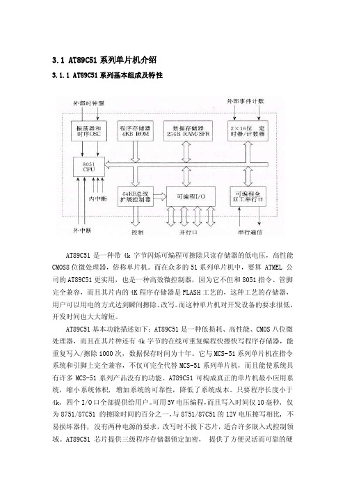
3.1 AT89C51系列单片机介绍3.1.1 AT89C51系列基本组成及特性AT89C51是一种带4k字节闪烁可编程可擦除只读存储器的低电压,高性能CMOS8位微处理器,俗称单片机。
而在众多的51系列单片机中,要算 ATMEL 公司的AT89C51更实用,也是一种高效微控制器,因为它不但和8051指令、管脚完全兼容,而且其片内的4K程序存储器是FLASH工艺的,这种工艺的存储器,用户可以用电的方式达到瞬间擦除、改写。
而这种单片机对开发设备的要求很低,开发时间也大大缩短。
AT89C51基本功能描述如下:AT89C51是一种低损耗、高性能、CMOS八位微处理器,而且在其片种还有4k字节的在线可重复编程快擦快写程序存储器,能重复写入/擦除1000次,数据保存时间为十年。
它与MCS-51系列单片机在指令系统和引脚上完全兼容,不仅可完全代替MCS-51系列单片机,而且能使系统具有许多MCS-51系列产品没有的功能。
AT89C51可构成真正的单片机最小应用系统,缩小系统体积, 增加系统的可靠性,降低了系统成本。
只要程序长度小于4k, 四个I/O口全部提供给用户。
可用5V电压编程,而且写入时间仅10毫秒, 仅为8751/87C51 的擦除时间的百分之一,与8751/87C51的12V电压擦写相比, 不易损坏器件, 没有两种电源的要求,改写时不拔下芯片,适合许多嵌入式控制领域。
AT89C51 芯片提供三级程序存储器锁定加密,提供了方便灵活而可靠的硬加密手段, 能完全保证程序或系统不被仿制。
另外,AT89C51 还具有MCS-51系列单片机的所有优点。
128×8 位内部RAM, 32 位双向输入输出线, 两个十六位定时器/计时器, 5个中断源, 两级中断优先级, 一个全双工异步串行口及时钟发生器等。
AT89C51有间歇、掉电两种工作模式。
间歇模式是由软件来设置的, 当外围器件仍然处于工作状态时, CPU可根据工作情况适时地进入睡眠状态, 内部RAM和所有特殊的寄存器值将保持不变。
at89c51

AT89C51简介AT89C51是一款由8051微控制器系列衍生的8位单片机。
它由Atmel公司开发,主要用于嵌入式系统和单板计算机中的应用。
AT89C51是一款非常常见的单片机,使用广泛,并且在市场上易于获得。
特性•8位CPU架构•4K字节的Flash存储器•128字节的RAM存储器•32个通用输入/输出引脚•2个计数器/定时器•6个中断源•电源电压范围:4.0V至6.0VAT89C51具有32个引脚,每个引脚都可以配置为输入或输出。
以下是一些重要的引脚功能:1.P0(引脚2至9):P0口是一个8位的双向通用I/O口。
在默认情况下,它被配置为准双向输入口。
用户可以通过设置相应的位来将其配置为输出端口。
2.P1(引脚10至17):P1口也是一个8位的双向通用I/O口。
3.P2(引脚21至28):P2口也是一个8位的双向通用I/O口,但是它还具有其他功能。
P2口可以用作从机模式的串行数据接口。
4.P3(引脚1、16、17):P3口是一个6位的双向通用I/O口。
它还具有其他特殊功能。
P3口的引脚1和引脚16用作外部中断源,引脚17用作时钟输入。
5.EA/VPP(引脚31):EA/VPP用于给单片机提供外部存储器的编程电压。
AT89C51单片机具有许多功能和特性,使其成为嵌入式系统设计的理想选择。
1.存储器:AT89C51具有4K字节的Flash存储器,用于存储程序和数据。
它还具有128字节的RAM存储器,用于临时存储数据。
2.计数器/定时器:AT89C51具有两个16位的计数器/定时器。
这些计数器可以用于计时、生成脉冲和测量时间间隔。
3.中断:AT89C51具有6个中断源,包括外部中断、定时器中断和串行通信中断。
中断可以帮助处理和响应实时事件。
4.串行通信:AT89C51支持串行通信协议,如UART协议。
它可以与其他设备进行数据通信,例如传感器或外部存储器。
5.低功耗模式:AT89C51具有多个节能模式,可最大限度地降低功耗。
AT89C51RE2-SLSUM;AT89C51RE2-RLTUM;AT89C51RE2-SLRUM;中文规格书,Datasheet资料
Figure 1. Block Diagram
Keyboard RxD_0 RxD_1 (1) BOOT Regulator 4K x8 POR / PFD ROM TxD_0 T2EX VCC PCA Vss TxD_1
ECI
T2
(2) (2) XTALA1 XTALA2 XTALB1(1) XTALB2 ALE/ PROG PSEN EA RD WR (2) (2) Timer 0 Timer 1 INT Ctrl CPU
P0.2/AD2 P0.3/AD3 35 34 33 32 31 30 29 P2.3/A11 P2.4/A12
P0.0/AD0 P2.1/A9
AT89C51RE2 PLCC44
18 19 20 21 22 23 24 25 26 27 28
P3.6/WR Tx_OCD P2.0/A8 P2.2/A10 P3.7/RD XTAL2 XTAL1 VSS
C51 CORE
(1)
(1) (1)
(1)
(3) (3)
EUART
RAM 256x8
Flash 128Kx8
XRAM
8192 x 8
PCA
Watch Dog Timer2 Keyboard POR PFD
EUART_1
IB-bus
Parallel I/O Ports &
External Bus Port 0 Port 1Port 2 Port 3 Port4 Port 5
• • • •
8-bit Flash Microcontroller AT89C51RE2
• • • • • • • • • •
• • • • • • • •
AT89C51单片机简介

AT89C51单片机简介AT89C51是一种带4K字节闪烁可编程可擦除只读存储器(FPEROM—FalshProgrammableandErasableReadOnlyMemory)的低电压,高性能CMOS8位微处理器,俗称单片机。
AT89C2051是一种带2K字节闪烁可编程可擦除只读存储器的单片机。
单片机的可擦除只读存储器可以反复擦除100次。
该器件采用ATMEL高密度非易失存储器制造技术制造,与工业标准的MCS-51指令集和输出管脚相兼容。
由于将多功能8位CPU和闪烁存储器组合在单个芯片中,ATMEL·5个中断源·可编程串行通道·低功耗的闲置和掉电模式·片内振荡器和时钟电路2.管脚说明:VCC:供电电压。
GND:接地。
P0口:P0口为一个8位漏级开路双向I/O口,每脚可吸收8TTL门电流。
当P1口的管脚第一次写1时,被定义为高阻输入。
P0能够用于外部程序数据存储器,它可以被定义为数据/地址的第八位。
在FIASH编程时,P0口作为原码输入口,当FIASH进行校验时,P0输出原码,此时P0P1门电流。
P1P2门电流,当口的16位口在P3P3口写入P3P3.0RXD(串行输入口)P3.1TXD(串行输出口)P3.2/INT0(外部中断0)P3.3/INT1(外部中断1)P3.4T0(记时器0外部输入)P3.5T1(记时器1外部输入)P3.6/WR(外部数据存储器写选通)P3.7/RD(外部数据存储器读选通)P3口同时为闪烁编程和编程校验接收一些控制信号。
FLASH0。
此时,/PSENXTAL1和XTAL2分别为反向放大器的输入和输出。
该反向放大器可以配置为片内振荡器。
石晶振荡和陶瓷振荡均可采用。
如采用外部时钟源驱动器件,XTAL2应不接。
有余输入至内部时钟信号要通过一个二分频触发器,因此对外部时钟信号的脉宽无任何要求,但必须保证脉冲的高低电平要求的宽度。
4.芯片擦除:整个PEROM阵列和三个锁定位的电擦除可通过正确的控制信号组合,并保持ALE管脚处于低电平10ms来完成。
at89c51中文资料_数据手册_参数

AT89C51是一种低功耗、高性能的CMOS 8位微型计算机,具有4Kbytes的Flash可编程只读 存储器(PEROM)。该设备使用Atmel的高密度非易失性存储器技术制造,与工业标准的 MCS-51指令集和pinout兼容。芯片上的闪存可以让程序内存在系统内重新编程,也可以 由一个召集人的非易失性内存程序员来重新编程。Atmel AT89C51是一种功能强大的微型 计算机,它将一个多用途的8位CPU与闪存芯片结合在一起,为许多嵌入式控制应用程序 提供了一种高灵活性和高性价比的解决方案。AT89C51提供了以下标准特性:4Kbytes的 Flash, 128字节的RAM, 32个I/O行,两AT89C51个16位的计时器/计数器,一个五个矢量的 二级中断架构,一个完整的双工串口,片上振荡器和时钟圈-cuitry。此外,AT89C51采用 静态逻辑设计,可将操作频率降至零,支持两种软件可选择的节能模式。空闲的适当操 作CPU,同时允许RAM、计时器/计数器、串行端口和中断系统继续运行。电源关闭模式 保存RAM内容,但冻结振荡器禁用所有其他芯片功能,直到下一个硬件复位。销 DescriptionVCCSupply voltage.GNDGround。端口0Port 0是一个8位开路双向I/O端口。作为 输出端口,每个引脚可以接收8个TTLAT89C51输入。当1被写入端口0时,这些引脚可以 作为高阻抗输入。端口0也可以配置为在访问外部pro-gram和数据内存期间的多路低阶地 址/数据总线。在这种模式下,P0具有内浆。端口0也在Flash编程期间接收代码字节,并 输出代码字节du环编程验证。AT89C51在程序验证过程中需要外部的pullups。端口1是一 个8位双向I/O端口,具有内部pullups。端口1输出缓冲区可以接收/源4个TTL输入。当1s被 写入端口1引脚时,它们被内部的脉冲拉高,并可作为输入。作为输入,外部被拉低的端 口1引脚会因为内部的pullups而变酸(IIL)。端口1也在flasups的8位双向I/O端口。端口2输出缓冲区可以接收/ 源4个TTL输入。当1s被写到端口2时,它们被内部的pullups拉得很高,可以用作输入。作 为输入,外部被拉低的端口2引脚会因为内部的脉冲而变酸。端口2在从外部程序内存获 取和访问使用16位地址的外部数据内存(MOVX @DPTR)期间发出高阶地址字节。在这个 应用中,当发射1s时,它使用强的内部拉升。在访问使用8位地址(MOVX @ RI)的外部数 据存储器时,端口2发出P2专AT89C51用函数寄存器的核心。端口2还在Flash编程和验证 过程中接收高阶地址位和somecontrol信号。端口3Port 3是一个8位双向I/O端口,具有内部 pullups。端口3输出缓冲区可以接收/源四个TTL输入。当1s被写到端口3时,它们被内部的 pullups拉得很高,可以用作输入。作为输入,外部被拉低的端口3引脚会因为pullups而变 酸(IIL)。端口3还具有AT89C51的各种特殊功能,如下所示在每次访问外部数据时都跳过 了pulse。如果需要,可以通过设置sfr位置8EH的0位来禁用ALE操作。在位集上,ALE只 在一个MOVX或MOVC指令中活动。否则,大头针就会弱拉高。如果微控制器处于外部 执行模式,则设置禁用“禁用”的位就没有效果。PSENProgram Store启用的是read strobe 到外部的pro-AT89C51gram内存。当AT89C51执行来自外部pro-gram内存的代码时,每个 machinecycle都会激活PSEN两次,除了在每次访问外部数据内存时跳过两次PSEN激 活。EA / VPPExternal访问启用AT89C51。必须将EA绑定到GND,以使设备能够从从从 0000H到FFFFH的外部pro-gram内存位置获取代码。然而,请注意,如果锁位1被编 程,EA将在复位时被内部锁住。EA应该绑定到VCC以执行内部程序。在Flash编程中,这 个pin还能接收12伏的编程实现volt-age (VPP),这是需要12伏VPP的部件。XTAL1Input输入到逆变振荡器放大器,输入到内部时 钟运行电路。XTAL2Output逆变振荡器放大器的输出。振荡器特性sxtal1和XTAL2分别是 逆变放大器的输入和输出,可以配置为使用asan片上振荡器,如图1所示。可以使用石英 晶体或陶瓷谐振器。要从外部时钟源驱动设备,XTAL2应该保持左连接,而XTAL1应该 被驱动,如图2所示。在外部时钟信号的工作周期中没有要求,因为内部时钟电路的输入 是通过两个触发器,但是最小和最大的电压高AT89C51和低的时间规格必须被观察。在 空闲模式下,CPU自动进入休眠状态,而所有的片上外围设备仍然处于活动状态。模式 是由软件调用的。在此模式下,片上RAM的内容和所有的spe函数寄存器都保持不变。空 闲模式可以通过任何启用的中断或硬件重置来终止。应该注意的是,当空闲被硬件 AT89C51重置终止时,设备通常会恢复程序执行,从它停止的地方开始,直到内部复位 算法控制之前的两个机器周期。在这种情况下,芯片上的硬件存储限制了对内部RAM的 访问,AT89C51但是对端口引脚的访问是不受限制的。为了消除AT89C51在空闲时对端口 pin进行意外写入的可能性,可以通过重置来终止,调用idleshnd的指令后面的指令不应该 是写入端口pin或外部内存的指令
AT89C51单片机简单介绍

AT89C51单片机简单介绍
AT89C51单片机是一款由Atmel公司生产出的基于8位MCS-51内核架构的单片机。
其内部包含大量的外设和接口,如8KB的Flash存储器、128字节的RAM、32个通用输入/输出引脚、三个16位定时器/计数器,还具备可编程的串行通讯接口UART、SPI、I2C总线控制等外设,使其在嵌入式系统中广泛应用。
AT89C51单片机拥有稳定、可靠的性能,主要应用于各种嵌入式系统中,例如:智能家居、仪器仪表、安防控制设备、工业自动化设备、医疗设备等。
1. 采用MCS-51内核架构,具有8位宽的数据总线和16位宽的地址总线;
2. 内置8KB的Flash存储器和128字节的RAM,可实现程序存储和数据处理;
3. 32个通用输入/输出引脚,可扩展各种外设和接口;
4. 内置三个16位定时器/计数器,可生成多种PWM波形,产生各种延时和定时功能;
5. 内置可编程的串行通讯接口UART,支持RS232、RS485通讯协议;
6. 支持SPI、I2C总线控制,可实现多种通讯方式;
7. 拥有多种中断模式和中断源,可实现多任务处理、多线程操作;
8. 采用低功耗设计,外部器件少,体积小,非常适合嵌入式系统应用。
最后,AT89C51单片机是一款性价比高、应用广泛、可靠稳定的单片机,是嵌入式系统设计师的不二之选。
AT89C51 DATASHEET
PQFP/TQFPFeatures•Compatible with MCS-51™ Products•4K Bytes of In-System Reprogrammable Flash Memory –Endurance: 1,000 Write/Erase Cycles •Fully Static Operation: 0 Hz to 24 MHz •Three-level Program Memory Lock •128 x 8-bit Internal RAM •32 Programmable I/O Lines •Two 16-bit Timer/Counters •Six Interrupt Sources•Programmable Serial Channel•Low-power Idle and Power-down ModesDescriptionThe AT89C51 is a low-power, high-performance CMOS 8-bit microcomputer with 4K bytes of Flash programmable and erasable read only memory (PEROM). The device is manufactured using Atmel’s high-density nonvolatile memory technology and is compatible with the industry-standard MCS-51 instruction set and pinout. The on-chip Flash allows the program memory to be reprogrammed in-system or by a conven-tional nonvolatile memory programmer. By combining a versatile 8-bit CPU with Flash on a monolithic chip, the Atmel AT89C51 is a powerful microcomputer which provides a highly-flexible and cost-effective solution to many embedded control applications.PDIPPin ConfigurationsPLCCBlock DiagramAT89C51The AT89C51 provides the following standard features: 4K bytes of Flash, 128 bytes of RAM, 32 I/O lines, two 16-bit timer/counters, a five vector two-level interrupt architecture, a full duplex serial port, on-chip oscillator and clock cir-cuitry. In addition, the AT89C51 is designed with static logic for operation down to zero frequency and supports two software selectable power saving modes. The Idle Mode stops the CPU while allowing the RAM, timer/counters, serial port and interrupt system to continue functioning. The Power-down Mode saves the RAM contents but freezes the oscillator disabling all other chip functions until the next hardware reset.Pin DescriptionVCCSupply voltage.GNDGround.Port 0Port 0 is an 8-bit open-drain bi-directional I/O port. As an output port, each pin can sink eight TTL inputs. When 1s are written to port 0 pins, the pins can be used as high-impedance inputs.Port 0 may also be configured to be the multiplexed low-order address/data bus during accesses to external pro-gram and data memory. In this mode P0 has internal pullups.Port 0 also receives the code bytes during Flash program-ming, and outputs the code bytes during program verification. External pullups are required during program verification.Port 1Port 1 is an 8-bit bi-directional I/O port with internal pullups. The Port 1 output buffers can sink/source four TTL inputs. When 1s are written to Port 1 pins they are pulled high by the internal pullups and can be used as inputs. As inputs, Port 1 pins that are externally being pulled low will source current (I IL) because of the internal pullups.Port 1 also receives the low-order address bytes during Flash programming and verification.Port 2Port 2 is an 8-bit bi-directional I/O port with internal pullups. The Port 2 output buffers can sink/source four TTL inputs. When 1s are written to Port 2 pins they are pulled high by the internal pullups and can be used as inputs. As inputs,Port 2 pins that are externally being pulled low will source current (I IL) because of the internal pullups.Port 2 emits the high-order address byte during fetches from external program memory and during accesses to external data memory that use 16-bit addresses (MOVX @ DPTR). In this application, it uses strong internal pullups when emitting 1s. During accesses to external data mem-ory that use 8-bit addresses (MOVX @ RI), Port 2 emits the contents of the P2 Special Function Register.Port 2 also receives the high-order address bits and some control signals during Flash programming and verification. Port 3Port 3 is an 8-bit bi-directional I/O port with internal pullups. The Port 3 output buffers can sink/source four TTL inputs. When 1s are written to Port 3 pins they are pulled high by the internal pullups and can be used as inputs. As inputs, Port 3 pins that are externally being pulled low will source current (I IL) because of the pullups.Port 3 also serves the functions of various special features of the AT89C51 as listed below:Port 3 also receives some control signals for Flash pro-gramming and verification.RSTReset input. A high on this pin for two machine cycles while the oscillator is running resets the device.Address Latch Enable output pulse for latching the low byte of the address during accesses to external memory. This pin is also the program pulse input (PROG) during Flash programming.In normal operation ALE is emitted at a constant rate of 1/6 the oscillator frequency, and may be used for external tim-ing or clocking purposes. Note, however, that one ALE Port Pin Alternate FunctionsP3.0RXD (serial input port)P3.1TXD (serial output port)P3.2INT0 (external interrupt 0)P3.3INT1 (external interrupt 1)P3.4T0 (timer 0 external input)P3.5T1 (timer 1 external input)P3.6WR (external data memory write strobe)P3.7RD (external data memory read strobe)pulse is skipped during each access to external Data Memory.If desired, ALE operation can be disabled by setting bit 0 of SFR location 8EH. With the bit set, ALE is active only dur-ing a MOVX or MOVC instruction. Otherwise, the pin is weakly pulled high. Setting the ALE-disable bit has no effect if the microcontroller is in external execution mode. PSENProgram Store Enable is the read strobe to external pro-gram memory.When the AT89C51 is executing code from external pro-gram memory, PSEN is activated twice each machine cycle, except that two PSEN activations are skipped during each access to external data memory.EA/VPPorder to enable the device to fetch code from external pro-gram memory locations starting at 0000H up to FFFFH. internally latched on reset.EA should be strapped to V CC for internal program executions.This pin also receives the 12-volt programming enable volt-age (V PP) during Flash programming, for parts that require 12-volt V PP.XTAL1Input to the inverting oscillator amplifier and input to the internal clock operating circuit.XTAL2Output from the inverting oscillator amplifier.Oscillator CharacteristicsXTAL1 and XTAL2 are the input and output, respectively, of an inverting amplifier which can be configured for use as an on-chip oscillator, as shown in Figure 1. Either a quartz crystal or ceramic resonator may be used. To drive the device from an external clock source, XTAL2 should be left unconnected while XTAL1 is driven as shown in Figure 2. There are no requirements on the duty cycle of the external clock signal, since the input to the internal clocking circuitry is through a divide-by-two flip-flop, but minimum and maxi-mum voltage high and low time specifications must be observed.Idle ModeIn idle mode, the CPU puts itself to sleep while all the on-chip peripherals remain active. The mode is invoked by software. The content of the on-chip RAM and all the spe-cial functions registers remain unchanged during this mode. The idle mode can be terminated by any enabled interrupt or by a hardware reset.It should be noted that when idle is terminated by a hard ware reset, the device normally resumes program execu-tion, from where it left off, up to two machine cycles before the internal reset algorithm takes control. On-chip hardware inhibits access to internal RAM in this event, but access to the port pins is not inhibited. To eliminate the possibility of an unexpected write to a port pin when Idle is terminated by reset, the instruction following the one that invokes Idle should not be one that writes to a port pin or to external memory.Figure 1. Oscillator ConnectionsNote:C1, C2 = 30 pF ± 10 pF for Crystals= 40 pF ±10 pF for Ceramic ResonatorsXT AL2GNDXT AL1Status of External Pins During Idle and Power-down ModesMode Program Memory ALE PSEN PORT0PORT1PORT2PORT3 Idle Internal11Data Data Data Data Idle External11Float Data Address Data Power-down Internal00Data Data Data Data Power-down External00Float Data Data DataAT89C51Figure 2. External Clock Drive ConfigurationPower-down ModeIn the power-down mode, the oscillator is stopped, and the instruction that invokes power-down is the last instruction executed. The on-chip RAM and Special Function Regis-ters retain their values until the power-down mode is terminated. The only exit from power-down is a hardware reset. Reset redefines the SFRs but does not change the on-chip RAM. The reset should not be activated before V CC is restored to its normal operating level and must be held active long enough to allow the oscillator to restart and stabilize.Program Memory Lock BitsOn the chip are three lock bits which can be left unpro-grammed (U) or can be programmed (P) to obtain the additional features listed in the table below.When lock bit 1 is programmed, the logic level at the EA pin is sampled and latched during reset. If the device is pow-ered up without a reset, the latch initializes to a random value, and holds that value until reset is activated. It is nec-essary that the latched value of EA be in agreement with the current logic level at that pin in order for the device tofunction properly.Lock Bit Protection ModesProgram Lock BitsProtection TypeLB1LB2LB31U U U No program lock features2P U U MOVC instructions executed from external program memory are disabled fromfetching code bytes from internal memory, EA is sampled and latched on reset,and further programming of the Flash is disabled3P P U Same as mode 2, also verify is disabled4P P P Same as mode 3, also external execution is disabledProgramming the FlashThe AT89C51 is normally shipped with the on-chip Flash memory array in the erased state (that is, contents = FFH) and ready to be programmed. The programming interface accepts either a high-voltage (12-volt) or a low-voltage (V CC) program enable signal. The low-voltage program-ming mode provides a convenient way to program the AT89C51 inside the user’s system, while the high-voltage programming mode is compatible with conventional third-party Flash or EPROM programmers.The AT89C51 is shipped with either the high-voltage or low-voltage programming mode enabled. The respective top-side marking and device signature codes are listed in the following table.The AT89C51 code memory array is programmed byte-by-byte in either programming mode. To program any non-blank byte in the on-chip Flash Memory, the entire memory must be erased using the Chip Erase Mode. Programming Algorithm: Before programming the AT89C51, the address, data and control signals should be set up according to the Flash programming mode table and Figure 3 and Figure 4. To program the AT89C51, take the following steps.1.Input the desired memory location on the addresslines.2.Input the appropriate data byte on the data lines.3.Activate the correct combination of control signals.4.Raise EA/V PP to 12V for the high-voltage program-ming mode.5.Flash array or the lock bits. The byte-write cycle isself-timed and typically takes no more than 1.5 ms.Repeat steps 1 through 5, changing the addressand data for the entire array or until the end of theobject file is reached.Data Polling: The AT89C51 features Data Polling to indi-cate the end of a write cycle. During a write cycle, an attempted read of the last byte written will result in the com-plement of the written datum on PO.7. Once the write cycle has been completed, true data are valid on all outputs, and the next cycle may begin. Data Polling may begin any time after a write cycle has been initiated.The progress of byte programming can also low after ALE goes high during programming to indicate BUSY. P3.4 is pulled high again when programming is done to indicate READY.Program Verify: If lock bits LB1 and LB2 have not been programmed, the programmed code data can be read back via the address and data lines for verification. The lock bits cannot be verified directly. Verification of the lock bits is achieved by observing that their features are enabled. Chip Erase: The entire Flash array is erased electrically by using the proper combination of control signals and by with all “1”s. The chip erase operation must be executed before the code memory can be re-programmed. Reading the Signature Bytes: The signature bytes are read by the same procedure as a normal verification of locations 030H, 031H, and 032H, except that P3.6 and P3.7 must be pulled to a logic low. The values returned are as follows.(030H) = 1EH indicates manufactured by Atmel(031H) = 51H indicates 89C51(032H) = FFH indicates 12V programming(032H) = 05H indicates 5V programmingProgramming InterfaceEvery code byte in the Flash array can be written and the entire array can be erased by using the appropriate combi-nation of control signals. The write operation cycle is self-timed and once initiated, will automatically time itself to completion.All major programming vendors offer worldwide support for the Atmel microcontroller series. Please contact your local programming vendor for the appropriate software revision.V PP = 12V V PP = 5VTop-side Mark A T89C51xxxxyyww A T89C51 xxxx-5 yywwSignature(030H) = 1EH(031H) = 51H(032H) =F FH (030H) = 1EH (031H) = 51H (032H) = 05HAT89C51Note:1.Figure 3. Programming the FlashFigure 4. Verifying the FlashFlash Programming ModesModeRSTPSENALE/PROGEA/V PPP2.6P2.7P3.6P3.7Write Code DataHLH/12VLHHHRead Code Data H L H H L L H H Write LockBit - 1HLH/12VHHHHBit - 2H L H/12V H H L LBit - 3H L H/12V H L H LChip Erase H LH/12V H L L LRead Signature Byte H L H H L L LL(1)Flash Programming and Verification Waveforms - High-voltage Mode (V PP = 12V)= 5V)P1.0-P1.7P2.0-P2.3ALE/PROGPORT 0EA/V PP P2.7(ENABLE)P3.4(RDY/BSY)P1.0-P1.7P2.0-P2.3ALE/PROGPORT 0EA/V PP P2.7(ENABLE)P3.4(RDY/BSY)AT89C51Flash Programming and Verification CharacteristicsT A = 0°C to 70°C, V CC = 5.0 ± 10%Symbol Parameter Min Max Units V PP(1)Programming Enable Voltage11.512.5V I PP(1)Programming Enable Current 1.0mA 1/t CLCL Oscillator Frequency324MHz t AVGL Address Setup to PROG Low48t CLCLt GHAX Address Hold after PROG48t CLCLt DVGL Data Setup to PROG Low48t CLCLt GHDX Data Hold after PROG48t CLCLt EHSH P2.7 (ENABLE) High to V PP48t CLCLt SHGL V PP Setup to PROG Low10µs t GHSL(1)V PP Hold after PROG10µs t GLGH PROG Width1110µs t AVQV Address to Data Valid48t CLCLt ELQV ENABLE Low to Data Valid48t CLCLt EHQZ Data Float after ENABLE048t CLCLt GHBL PROG High to BUSY Low 1.0µs t WC Byte Write Cycle Time 2.0msAbsolute Maximum Ratings*Notes:1.Under steady state (non-transient) conditions, I OL must be externally limited as follows:Maximum I OL per port pin: 10 mAMaximum I OL per 8-bit port: Port 0: 26 mA Ports 1, 2, 3: 15 mAMaximum total I OL for all output pins: 71 mAIf I OL exceeds the test condition, V OL may exceed the related specification. Pins are not guaranteed to sink current greater than the listed test conditions.2.Minimum V CC for Power-down is 2V .Operating Temperature..................................-55°C to +125°C *NOTICE:Stresses beyond those listed under “AbsoluteMaximum Ratings” may cause permanent dam-age to the device. This is a stress rating only and functional operation of the device at these or any other conditions beyond those indicated in the operational sections of this specification is not implied. Exposure to absolute maximum rating conditions for extended periods may affect device reliability.Storage Temperature.....................................-65°C to +150°C Voltage on Any Pinwith Respect to Ground.....................................-1.0V to +7.0V Maximum Operating Voltage ............................................6.6VDC Output Current......................................................15.0 mADC CharacteristicsT A = -40°C to 85°C, V CC = 5.0V ± 20% (unless otherwise noted)Symbol Parameter Condition Min Max Units V IL Input Low-voltage (Except EA)-0.50.2 V CC - 0.1V V IL1Input Low-voltage (EA)-0.50.2 V CC - 0.3V V IH Input High-voltage (Except XT AL1, RST)0.2 V CC + 0.9V CC + 0.5V V IH1Input High-voltage(XTAL1, RST)0.7 V CCV CC + 0.5V V OL Output Low-voltage (1) (Ports 1,2,3)I OL = 1.6 mA 0.45V V OL1Output Low-voltage (1)(Port 0, ALE, PSEN)I OL = 3.2 mA0.45V V OH Output High-voltage(Ports 1,2,3, ALE, PSEN)I OH = -60 µA, V CC = 5V ± 10%2.4V I OH = -25 µA 0.75 V CC V I OH = -10 µA0.9 V CC V V OH1Output High-voltage(Port 0 in External Bus Mode)I OH = -800 µA, V CC = 5V ± 10%2.4V I OH = -300 µA 0.75V CC V I OH = -80 µA0.9 V CCV I IL Logical 0 Input Current (Ports 1,2,3)V IN = 0.45V-50µA I TL Logical 1 to 0 T ransition Current (Ports 1,2,3)V IN = 2V , VCC = 5V ± 10%-650µA I LI Input Leakage Current (Port 0, EA)0.45 <V IN < V CC±10µA RRST Reset Pull-down Resistor 50300K ΩC IOPin Capacitance Test Freq. = 1 MHz, T A = 25°C 10pF I CCPower Supply CurrentActive Mode, 12 MHz 20mA Idle Mode, 12 MHz 5mA Power-down Mode (2)V CC = 6V 100µA V CC = 3V40µAAT89C5111AC CharacteristicsUnder operating conditions, load capacitance for Port 0, ALE/PROG, and PSEN = 100 pF; load capacitance for all other outputs = 80 pF.External Program and Data Memory CharacteristicsSymbol Parameter12 MHz Oscillator16 to 24 MHz Oscillator Units MinMaxMin Max 1/t CLCL Oscillator Frequency 024MHz t LHLL ALE Pulse Width 1272t CLCL -40ns t AVLL Address Valid to ALE Low 43t CLCL -13ns t LLAX Address Hold after ALE Low 48t CLCL -20ns t LLIV ALE Low to Valid Instruction In 2334t CLCL -65ns t LLPL ALE Low to PSEN Low 43t CLCL -13ns t PLPH PSEN Pulse Width2053t CLCL -20ns t PLIV PSEN Low to Valid Instruction In 1453t CLCL -45ns t PXIX Input Instruction Hold after PSEN 0ns t PXIZ Input Instruction Float after PSEN 59t CLCL -10ns t PXAV PSEN to Address Valid 75t CLCL -8ns t AVIV Address to Valid Instruction In 3125t CLCL -55ns t PLAZ PSEN Low to Address Float 1010ns t RLRH RD Pulse Width 4006t CLCL -100ns t WLWH WR Pulse Width 4006t CLCL -100ns t RLDV RD Low to Valid Data In 2525t CLCL -90ns t RHDX Data Hold after RD 0ns t RHDZ Data Float after RD 972t CLCL -28ns t LLDV ALE Low to Valid Data In 5178t CLCL -150ns t AVDV Address to Valid Data In 5859t CLCL -165ns t LLWL ALE Low to RD or WR Low 2003003t CLCL -503t CLCL +50ns t AVWL Address to RD or WR Low 2034t CLCL -75ns t QVWX Data Valid to WR Transition 23t CLCL -20ns t QVWH Data Valid to WR High 4337t CLCL -120ns t WHQX Data Hold after WR 33t CLCL -20ns t RLAZ RD Low to Address Float 00ns t WHLHRD or WR High to ALE High43123t CLCL -20t CLCL +25nsAT89C5112External Program Memory Read CycleExternal Data Memory Read CycleAT89C5113External Data Memory Write CycleExternal Clock Drive WaveformsExternal Clock DriveSymbol ParameterMin Max Units 1/t CLCL Oscillator Frequency 024MHz t CLCL Clock Period 41.6ns t CHCX High Time 15ns t CLCX Low Time 15ns t CLCH Rise Time 20ns t CHCLFall Time20nsAT89C5114Shift Register Mode Timing WaveformsAC Testing Input/Output Waveforms (1)Note:1.AC Inputs during testing are driven at V CC - 0.5V for alogic 1 and 0.45V for a logic 0. Timing measurements are made at V IH min. for a logic 1 and V IL max. for a logic 0.Float Waveforms (1)Note:1.For timing purposes, a port pin is no longer floatingwhen a 100 mV change from load voltage occurs. A port pin begins to float when 100 mV change from the loaded V OH /V OL level occurs.Serial Port Timing: Shift Register Mode Test Conditions(V CC = 5.0 V ± 20%; Load Capacitance = 80 pF)Symbol Parameter12 MHz OscVariable Oscillator UnitsMin MaxMin Maxt XLXL Serial Port Clock Cycle Time1.012t CLCL µs t QVXH Output Data Setup to Clock Rising Edge 70010t CLCL -133ns t XHQX Output Data Hold after Clock Rising Edge 502t CLCL -117ns t XHDX Input Data Hold after Clock Rising Edge 0ns t XHDVClock Rising Edge to Input Data Valid70010t CLCL -133nsALEINSTRUCTIONCLOCKAT89C5115Ordering InformationSpeed (MHz)Power Supply Ordering Code Package Operation Range 125V ± 20%A T89C51-12AC 44A Commercial A T89C51-12JC 44J (0°C to 70°C)A T89C51-12PC 40P6A T89C51-12QC 44Q A T89C51-12AI 44A Industrial A T89C51-12JI 44J (-40°C to 85°C)A T89C51-12PI 40P6A T89C51-12QI44Q 165V ± 20%A T89C51-16AC 44A Commercial A T89C51-16JC 44J (0°C to 70°C)A T89C51-16PC 40P6A T89C51-16QC 44Q A T89C51-16AI 44A Industrial A T89C51-16JI 44J (-40°C to 85°C)A T89C51-16PI 40P6A T89C51-16QI44Q 205V ± 20%A T89C51-20AC 44A Commercial A T89C51-20JC 44J (0°C to 70°C)A T89C51-20PC 40P6A T89C51-20QC 44Q A T89C51-20AI 44A Industrial A T89C51-20JI 44J (-40°C to 85°C)A T89C51-20PI 40P6A T89C51-20QI44Q 245V ± 20%A T89C51-24AC 44A Commercial A T89C51-24JC 44J (0°C to 70°C)A T89C51-24PC 40P6A T89C51-24QC 44Q A T89C51-24AI 44A Industrial A T89C51-24JI 44J (-40°C to 85°C)A T89C51-24PI 40P6A T89C51-24QI44QPackage Type44A 44-lead, Thin Plastic Gull Wing Quad Flatpack (TQFP)44J 44-lead, Plastic J-leaded Chip Carrier (PLCC)40P640-lead, 0.600” Wide, Plastic Dual Inline Package (PDIP)44Q44-lead, Plastic Gull Wing Quad Flatpack (PQFP)AT89C5116Packaging Information© Atmel Corporation 2000.Atmel Corporation makes no warranty for the use of its products, other than those expressly contained in the Company’s standard war-ranty which is detailed in Atmel’s Terms and Conditions located on the Company’s web site. The Company assumes no responsibility for any errors which may appear in this document, reserves the right to change devices or specifications detailed herein at any time without notice, and does not make any commitment to update the information contained herein. No licenses to patents or other intellectual prop-erty of Atmel are granted by the Company in connection with the sale of Atmel products, expressly or by implication. Atmel’s products are not authorized for use as critical components in life support devices or systems.Atmel HeadquartersAtmel OperationsCorporate Headquarters2325 Orchard Parkway San Jose, CA 95131TEL (408) 441-0311FAX (408) 487-2600EuropeAtmel U.K., Ltd.Coliseum Business Centre Riverside WayCamberley, Surrey GU15 3YL EnglandTEL (44) 1276-686-677FAX (44) 1276-686-697AsiaAtmel Asia, Ltd.Room 1219Chinachem Golden Plaza 77 Mody Road Tsimhatsui East Kowloon Hong KongTEL (852) 2721-9778FAX (852) 2722-1369JapanAtmel Japan K.K.9F, Tonetsu Shinkawa Bldg.1-24-8 ShinkawaChuo-ku, Tokyo 104-0033JapanTEL (81) 3-3523-3551FAX (81) 3-3523-7581Atmel Colorado Springs1150 E. Cheyenne Mtn. Blvd.Colorado Springs, CO 80906TEL (719) 576-3300FAX (719) 540-1759Atmel RoussetZone Industrielle13106 Rousset Cedex FranceTEL (33) 4-4253-6000FAX (33) 4-4253-6001Fax-on-DemandNorth America:1-(800) 292-8635International:1-(408) 441-0732e-mailliterature@Web Site BBS1-(408) 436-43090265G–02/00/xMMarks bearing ® and/or ™ are registered trademarks and trademarks of Atmel Corporation.Terms and product names in this document may be trademarks of others.This datasheet has been download from: Datasheets for electronics components.。
AT89C51单片机的介绍——最常用的51芯片

AT89C51单片机的介绍——最常用的51芯片AT89C51是一种带4K字节闪烁可编程可擦除只读存储器(FPEROM—Falsh Programmable and Erasable Read Only Memory)的低电压,高性能CMOS8位微处理器,俗称单片机。
该器件采用ATMEL高密度非易失存储器制造技术制造,与工业标准的MCS-51指令集和输出管脚相兼容。
由于将多功能8位CPU和闪烁存储器组合在单个芯片中,ATMEL的AT89C51是一种高效微控制器,为很多嵌入式控制系统提供了一种灵活性高且价廉的方案。
1.主要特性:·与MCS-51 兼容·4K字节可编程闪烁存储器寿命:1000写/擦循环数据保留时间:10年·全静态工作:0Hz-24Hz·三级程序存储器锁定·128*8位内部RAM·32可编程I/O线·两个16位定时器/计数器·5个中断源·可编程串行通道·低功耗的闲置和掉电模式·片内振荡器和时钟电路2.管脚说明:VCC:供电电压。
GND:接地。
P0口:P0口为一个8位漏级开路双向I/O口,每脚可吸收8TTL门电流。
当P1口的管脚第一次写1时,被定义为高阻输入。
P0能够用于外部程序数据存储器,它可以被定义为数据/地址的第八位。
在FIASH编程时,P0 口作为原码输入口,当FIASH进行校验时,P0输出原码,此时P0外部必须被拉高。
P1口:P1口是一个内部提供上拉电阻的8位双向I/O口,P1口缓冲器能接收输出4TTL门电流。
P1口管脚写入1后,被内部上拉为高,可用作输入,P1口被外部下拉为低电平时,将输出电流,这是由于内部上拉的缘故。
在FLASH编程和校验时,P1口作为第八位地址接收。
P2口:P2口为一个内部上拉电阻的8位双向I/O口,P2口缓冲器可接收,输出4个TTL门电流,当P2口被写“1”时,其管脚被内部上拉电阻拉高,且作为输入。
AT89C51芯片介绍

AT89C51 芯片介绍
AT89C51 是一种带4K 字节闪烁可编程可擦除只读存储器(FPEROMFalsh Programmable and Erasable Read Only Memory)的低电压,高性能CMOS8 位
微处理器,俗称单片机。
该器件采用ATMEL 高密度非易失存储器制造技术制造,与工业标准的MCS-51 指令集和输出管脚相兼容。
由于将多功能8 位CPU 和闪烁存储器组合在单个芯片中,ATMEL 的AT89C51 是一种高效微控
制器,为很多嵌入式控制系统提供了一种灵活性高且价廉的方案。
1.主要特性:
-与MCS-51 兼容
-4K 字节可编程闪烁存储器
寿命:1000 写/擦循环
数据保留时间:10 年
-全静态工作:0Hz-24Hz
-三级程序存储器锁定。
at89c51中文资料_数据手册_参数
万联芯城 电子元器件物料全国供应,专业提 供电子元器件原装现货产品,1 片起订,价格优势明显,电子元 器件采购网万联芯城目前为长电科技,顺络电子,先科 ST 等多 家知名原厂的指定授权代理商,专为客户提供电子元器件配单业 务,提交物料清单即可当天报价当天发货,点击进入万联芯城。
AT89C51是一种低功耗、高性能的CMOS 8位微型计算机,具有4Kbytes的Flash可编程只读 存储器(PEROM)。该设备使用Atmel的高密度非易失性存储器技术制造,与工业标准的 MCS-51指令集和pinout兼容。芯片上的闪存可以让程序内存在系统内重新编程,也可以 由一个召集人的非易失性内存程序员来重新编程。Atmel AT89C51是一种功能强大的微型 计算机,它将一个多用途的8位CPU与闪存芯片结合在一起,为许多嵌入式控制应用程序 提供了一种高灵活性和高性价比的解决方案。AT89C51提供了以下标准特性:4Kbytes的 Flash, 128字节的RAM, 32个I/O行,两AT89C51个16位的计时器/计数器,一个五个矢量的 二级中断架构,一个完整的双工串口,片上振荡器和时钟圈-cuitry。此外,AT89C51采用 静态逻辑设计,可将操பைடு நூலகம்频率降至零,支持两种软件可选择的节能模式。空闲的适当操 作CPU,同时允许RAM、计时器/计数器、串行端口和中断系统继续运行。电源关闭模式 保存RAM内容,但冻结振荡器禁用所有其他芯片功能,直到下一个硬件复位。销 DescriptionVCCSupply voltage.GNDGround。端口0Port 0是一个8位开路双向I/O端口。作为 输出端口,每个引脚可以接收8个TTLAT89C51输入。当1被写入端口0时,这些引脚可以 作为高阻抗输入。端口0也可以配置为在访问外部pro-gram和数据内存期间的多路低阶地 址/数据总线。在这种模式下,P0具有内浆。端口0也在Flash编程期间接收代码字节,并 输出代码字节du环编程验证。AT89C51在程序验证过程中需要外部的pullups。端口1是一 个8位双向I/O端口,具有内部pullups。端口1输出缓冲区可以接收/源4个TTL输入。当1s被 写入端口1引脚时,它们被内部的脉冲拉高,并可作为输入。作为输入,外部被拉低的端 口1引脚会因为内部的pullups而变酸(IIL)。端口1也在flash编程和验证过程中接收低阶地址 字节。端口2Port 2是一个带有内部pullups的8位双向I/O端口。端口2输出缓冲区可以接收/ 源4个TTL输入。当1s被写到端口2时,它们被内部的pullups拉得很高,可以用作输入。作 为输入,外部被拉低的端口2引脚会因为内部的脉冲而变酸。端口2在从外部程序内存获 取和访问使用16位地址的外部数据内存(MOVX @DPTR)期间发出高阶地址字节。在这个 应用中,当发射1s时,它使用强的内部拉升。在访问使用8位地址(MOVX @ RI)的外部数 据存储器时,端口2发出P2专AT89C51用函数寄存器的核心。端口2还在Flash编程和验证 过程中接收高阶地址位和somecontrol信号。端口3Port 3是一个8位双向I/O端口,具有内部 pullups。端口3输出缓冲区可以接收/源四个TTL输入。当1s被写到端口3时,它们被内部的 pullups拉得很高,可以用作输入。作为输入,外部被拉低的端口3引脚会因为pullups而变 酸(IIL)。端口3还具有AT89C51的各种特殊功能,如下所示在每次访问外部数据时都跳过 了pulse。如果需要,可以通过设置sfr位置8EH的0位来禁用ALE操作。在位集上,ALE只 在一个MOVX或MOVC指令中活动。否则,大头针就会弱拉高。如果微控制器处于外部 执行模式,则设置禁用“禁用”的位就没有效果。PSENProgram Store启用的是read strobe 到外部的pro-AT89C51gram内存。当AT89C51执行来自外部pro-gram内存的代码时,每个 machinecycle都会激活PSEN两次,除了在每次访问外部数据内存时跳过两次PSEN激 活。EA / VPPExternal访问启用AT89C51。必须将EA绑定到GND,以使设备能够从从从 0000H到FFFFH的外部pro-gram内存位置获取代码。然而,请注意,如果锁位1被编 程,EA将在复位时被内部锁住。EA应该绑定到VCC以执行内部程序。在Flash编程中,这 个pin还能接收12伏的编程实现volt-age (VPP),这是需要12伏VPP的部件。XTAL1Input输入到逆变振荡器放大器,输入到内部时 钟运行电路。XTAL2Output逆变振荡器放大器的输出。振荡器特性sxtal1和XTAL2分别是 逆变放大器的输入和输出,可以配置为使用asan片上振荡器,如图1所示。可以使用石英 晶体或陶瓷谐振器。要从外部时钟源驱动设备,XTAL2应该保持左连接,而XTAL1应该 被驱动,如图2所示。在外部时钟信号的工作周期中没有要求,因为内部时钟电路的输入 是通过两个触发器,但是最小和最大的电压高AT89C51和低的时间规格必须被观察。在 空闲模式下,CPU自动进入休眠状态,而所有的片上外围设备仍然处于活动状态。模式 是由软件调用的。在此模式下,片上RAM的内容和所有的spe函数寄存器都保持不变。空 闲模式可以通过任何启用的中断或硬件重置来终止。应该注意的是,当空闲被硬件 AT89C51重置终止时,设备通常会恢复程序执行,从它停止的地方开始,直到内部复位 算法控制之前的两个机器周期。在这种情况下,芯片上的硬件存储限制了对内部RAM的 访问,AT89C51但是对端口引脚的访问是不受限制的。为了消除AT89C51在空闲时对端口 pin进行意外写入的可能性,可以通过重置来终止,调用idleshnd的指令后面的指令不应该 是写入端口pin或外部内存的指令
单片机AT89C51

AT89C51是一种带4K字节闪烁可编程可擦除只读存储器(FPEROM—Falsh Programmable and Erasable Read Only Memory)的低电压,高性能CMOS8位微处理器,俗称单片机。
该器件采用ATMEL高密度非易失存储器制造技术制造,与工业标准的MCS-51指令集和输出管脚相兼容。
由于将多功能8位CPU和闪烁存储器组合在单个芯片中,ATMEL的AT89C51是一种高效微控制器,为很多嵌入式控制系统提供了一种灵活性高且价廉的方案。
1.主要特性:·8031 CPU与MCS-51 兼容· 4K字节可编程FLASH存储器(寿命:1000写/擦循环)· 全静态工作:0Hz-24KHz· 三级程序存储器保密锁定· 128*8位内部RAM· 32条可编程I/O线· 两个16位定时器/计数器·6个中断源· 可编程串行通道· 低功耗的闲置和掉电模式· 片内振荡器和时钟电路2.管脚说明:VCC:供电电压。
GND:接地。
P0口:P0口为一个8位漏级开路双向I/O口,每脚可吸收8TTL门电流。
当P1口的管脚第一次写1时,被定义为高阻输入。
P0能够用于外部程序数据存储器,它可以被定义为数据/地址的第八位。
在FIASH 编程时,P0 口作为原码输入口,当FIASH进行校验时,P0输出原码,此时P0外部必须被拉高。
P1口:P1口是一个内部提供上拉电阻的8位双向I/O口,P1口缓冲器能接收输出4TTL门电流。
P1口管脚写入1后,被内部上拉为高,可用作输入,P1口被外部下拉为低电平时,将输出电流,这是由于内部上拉的缘故。
在FLASH编程和校验时,P1口作为第八位地址接收。
P2口:P2口为一个内部上拉电阻的8位双向I/O口,P2口缓冲器可接收,输出4个TTL门电流,当P2口被写“1”时,其管脚被内部上拉电阻拉高,且作为输入。
AT89C51单片机的结构单片机资料
AT89C51单片机的结构单片机资料AT89C51是一种常用的8位单片机,具有可编程特性和丰富的外设接口,被广泛应用于各种电子设备中。
本文将介绍AT89C51单片机的结构和相关资料。
一、引言在现代电子产品中,单片机扮演着重要的角色,它能够实现复杂的功能,并且具有体积小、功耗低等优点。
AT89C51单片机是一种典型的8位单片机,具有高性能和可靠性,成为许多电子设计师的首选。
二、AT89C51单片机结构AT89C51单片机是基于CMOS技术的,并且采用了Harvard结构。
它由四个主要部分组成:中央处理器(CPU)、存储器、输入/输出接口(I/O)和定时/计数器。
1. 中央处理器(CPU)AT89C51单片机的CPU是一块高性能的8位微处理器,工作频率可达到最高12MHz。
它内部集成了ALU(算术逻辑单元)、寄存器、指令译码器和程序计数器等。
2. 存储器AT89C51单片机具有3种类型的存储器:Flash程序存储器、RAM 数据存储器和EEPROM数据存储器。
- Flash程序存储器用于存储程序代码,可通过编程器进行擦写和编程。
- RAM数据存储器用于临时存储数据,其容量为128字节。
- EEPROM数据存储器用于存储非易失性数据,其容量为4KB。
3. 输入/输出接口(I/O)AT89C51单片机具有4个I/O口,每个口可配置为输入或输出。
它们可与外围设备进行数据交换,如传感器、LED、LCD等。
4. 定时/计数器AT89C51单片机具有两个定时/计数器,可用于实现时间控制和计数功能。
它们可以设置不同的工作模式,并具有多种中断功能。
三、单片机资料为了更好地开发和应用AT89C51单片机,我们需要获取单片机的相关资料。
1. 数据手册单片机的数据手册是我们了解其内部结构和特性的重要参考资料。
它包含了单片机的详细规格、引脚图、寄存器说明、指令集等内容。
2. 开发工具在使用AT89C51单片机进行开发时,我们需要下载和安装相应的开发工具。
单片机简介_AT89C51中文资料

单片机简介_AT89C51中文资料单片机是嵌入式系统中重要的组成部分,它是一种具有特定功能并带有输入输出端口的微型计算机系统。
单片机的内部集成了CPU、RAM、ROM、I/O接口等部件,具有小体积、低功耗和高集成度等优点,被广泛应用于各种工业控制、家具控制以及电子仪表等领域。
AT89C51是一种常见的单片机,下面将对它进行详细介绍。
一、AT89C51的基本介绍AT89C51是一款由Atmel公司生产的8位单片机,它采用CMOS技术制造,具有16KB FLASH程序存储器和512B RAM数据存储器。
该单片机支持包括ISP(In-System-Programming)、IAP(In-Application-Programming)、DebugWire在内的多种编程方式,可用于各种应用领域,如汽车电子、家用电器、计算机外围设备、物流跟踪等。
AT89C51的主要特征:1、8位8051微控制器架构;2、具有16KB程序存储器和512B数据存储器;3、支持ISP、IAP和DebugWire等多种编程方式;4、支持12MHz内部晶体振荡器和外接振荡器,外接时钟频率为0~24MHz;5、支持一般I/O和特殊功能I/O,如双重中断、三重定时器等;6、可升级固件程序。
AT89C51共有40个引脚,分别是VCC、GND、P0.0~P0.7、P1.0~P1.7、P2.0~P2.7、P3.0~P3.7、RST、ALE、EA、PSEN、XTAL1、XTAL2,其中VCC是芯片的正电源,GND是芯片的负电源。
1、ISP编程方式:ISP编程即在芯片内部直接进行编程,无需将芯片取出进行编程。
这种编程方式需要使用ISP编程器和软件,将芯片与编程器连接后,在电脑上设置好所需的程序,即可进行编程。
2、IAP编程方式:IAP编程即在芯片内部进行程序更新、修改等操作,无需替换整个芯片。
该编程方式适用于已经安装在板子上的芯片,如果需要更新程序,直接通过串口通信上传新程序即可,无需拆卸芯片。
单片机简介 AT89C51中文资料

4.1 单片机介绍:单片机是指一个集成在一块芯片上的完整计算机系统。
尽管他的大部分功能集成在一块小芯片上,但是它具有一个完整计算机所需要的大部分部件:CPU、内存、内部和外部总线系统,目前大部分还会具有外存。
同时集成诸如通讯接口、定时器,实时时钟等外围设备。
而现在最强大的单片机系统甚至可以将声音、图像、网络、复杂的输入输出系统集成在一块芯片上。
单片机也被称为微控制器(Microcontroler),是因为它最早被用在工业控制领域。
单片机由芯片内仅有CPU的专用处理器发展而来。
最早的设计理念是通过将大量外围设备和CPU集成在一个芯片中,使计算机系统更小,更容易集成进复杂的而对提及要求严格的控制设备当中。
INTEL的Z80是最早按照这种思想设计出的处理器,从此以后,单片机和专用处理器的发展便分道扬镳。
早期的单片机都是8位或4位的。
其中最成功的是INTEL的8031,因为简单可靠而性能不错获得了很大的好评。
此后在8031上发展出了MCS51系列单片机系统。
基于这一系统的单片机系统直到现在还在广泛使用。
随着工业控制领域要求的提高,开始出现了16位单片机,但因为性价比不理想并未得到很广泛的应用。
90年代后随着消费电子产品大发展,单片机技术得到了巨大的提高。
随着INTEL i960系列特别是后来的ARM系列的广泛应用,32位单片机迅速取代16位单片机的高端地位,并且进入主流市场。
而传统的8位单片机的性能也得到了飞速提高,处理能力比起80年代提高了数百倍。
目前,高端的32位单片机主频已经超过300MHz,性能直追90年代中期的专用处理器,而普通的型号出厂价格跌落至1美元,最高端的型号也只有10美元。
当代单片机系统已经不再只在裸机环境下开发和使用,大量专用的嵌入式操作系统被广泛应用在全系列的单片机上。
而在作为掌上电脑和手机核心处理的高端单片机甚至可以直接使用专用的Windows和Linux操作系统。
单片机比专用处理器更适合应用于嵌入式系统,因此它得到了最多的应用。