电源控制芯片2N7002资料
2N7002中文资料

1.Product profile1.1General descriptionN-channel enhancement mode Field-Effect Transistor (FET) in a plastic package using Trench MOSFET technology.1.2Features and benefits⏹Suitable for logic level gate drive sources ⏹Very fast switching⏹Surface-mounted package ⏹Trench MOSFET technology1.3Applications⏹Logic level translators⏹High-speed line drivers1.4Quick reference data2.Pinning information2N700260 V, 300 mA N-channel Trench MOSFETRev. 7 — 8 September 2011Product data sheetTable 1.Quick reference dataSymbol ParameterConditions Min Typ Max Unit V DS drain-source voltage 25°C ≤T j ≤150°C--60V I D drain currentV GS =10V; T sp =25°C;see Figure 1; see Figure 3--300mA P tot total power dissipation T sp =25°C;see Figure 2--0.83W Static characteristicsR DSondrain-source on-state resistanceV GS =10V; I D =500mA; T j =25°C; see Figure 6; see Figure 8- 2.85ΩTable 2.Pinning information Pin Symbol Description Simplified outlineGraphic symbol1G gate SOT23 (TO-236AB)2S source 3Ddrain1233.Ordering information4.Marking[1]% = placeholder for manufacturing site code5.Limiting valuesTable 3.Ordering informationType numberPackage NameDescriptionVersion 2N7002TO-236ABplastic surface-mounted package; 3 leadsSOT23Table 4.Marking codesType numberMarking code [1]2N700212%Table 5.Limiting valuesIn accordance with the Absolute Maximum Rating System (IEC 60134).Symbol ParameterConditions Min Max Unit V DS drain-source voltage 25°C ≤T j ≤150°C-60V V DGR drain-gate voltage 25°C ≤T j ≤150°C; R GS =20k Ω-60V V GS gate-source voltage -3030V V GSM peak gate-source voltage pulsed; t p ≤50µs; δ=0.25-4040V I Ddrain currentV GS =10V; T sp =25°C;see Figure 1; see Figure 3-300mA V GS =10V; T sp =100°C; see Figure 1-190mA I DM peak drain current pulsed; t p ≤10µs; T sp =25°C;see Figure 3- 1.2A P tot total power dissipation T sp =25°C;see Figure 2-0.83W T j junction temperature -65150°C T stg storage temperature -65150°C Source-drain diodeI S source current T sp =25°C-300mA I SMpeak source currentpulsed; t p ≤10µs; T sp =25°C - 1.2A6.Thermal characteristicsTable 6.Thermal characteristicsSymbol Parameter ConditionsMin Typ Max Unit R th(j-a)thermal resistance from junction to ambientMounted on a printed-circuit board; minimum footprint ; vertical in still air--350K/WR th(j-sp)thermal resistance from junction to solder pointsee Figure 4--150K/W7.CharacteristicsTable 7.CharacteristicsSymbol Parameter Conditions Min Typ Max Unit Static characteristicsV(BR)DSS drain-sourcebreakdown voltage I D=10µA; V GS=0V; T j=25°C60--V I D=10µA; V GS=0V; T j=-55°C55--VV GSth gate-source thresholdvoltage I D=0.25mA;V DS=V GS; T j=25°C;see Figure 9; see Figure 1012 2.5VI D=0.25mA;V DS=V GS; T j=150°C;see Figure 9; see Figure 100.6--VI D=0.25mA;V DS=V GS; T j=-55°C;see Figure 9; see Figure 10-- 2.75VI DSS drain leakage current V DS=48V;V GS=0V; T j=25°C-0.011µAV DS=48V;V GS=0V; T j=150°C--10µA I GSS gate leakage current V GS=15V; V DS=0V; T j=25°C-10100nAV GS=-15V;V DS=0V; T j=25°C-10100nAR DSon drain-source on-stateresistance V GS=10V; I D=500mA; T j=25°C;see Figure 6; see Figure 8- 2.85ΩV GS=10V; I D=500mA; T j=150°C;see Figure 6; see Figure 8--9.25ΩV GS=4.5V;I D=75mA;T j=25°C;seeFigure 6; see Figure 8- 3.8 5.3ΩDynamic characteristicsC iss input capacitance V DS=10V;f=1MHz;V GS=0V;T j=25°C -3150pFC oss output capacitance- 6.830pF C rss reverse transfercapacitance- 3.510pFt on turn-on time V GS=10V; V DS=50V;R L=250Ω;R G(ext)=50Ω; R GS=50Ω- 2.510nst off turn-off time-1115ns Source-drain diodeV SD source-drain voltage I S=300mA;V GS=0V;T j=25°C;seeFigure 11-0.85 1.5VQ r recovered charge V GS=0V;I S=300mA;dI S/dt=-100A/µs -30-nCt rr reverse recovery time-30-ns8.Package outlinePlastic surface-mounted package; 3 leads SOT23Fig 13.Package outline SOT23 (TO-236AB)9.Soldering10.Revision historyTable 8.Revision historyDocument ID Release date Data sheet status Change notice Supersedes2N7002 v.720110908Product data sheet-2N7002 v.6 Modifications:•The format of this data sheet has been redesigned to comply with the new identity guidelinesof NXP Semiconductors.•Legal texts have been adapted to the new company name where appropriate.2N7002 v.620060428Product data sheet2N7002 v.52N7002 v.520051115Product data sheet2N7002 v.42N7002 v.420050426Product data sheet2N7002 v.32N7002 v.320000727Product specification HZG3362N7002 v.22N7002 v.219970617Product specification2N7002 v.12N7002 v.119901031Product specification--11.Legal information11.1Data sheet status[1]Please consult the most recently issued document before initiating or completing a design.[2]The term 'short data sheet' is explained in section "Definitions".[3]The product status of device(s) described in this document may have changed since this document was published and may differ in case of multiple devices. The latest productstatus information is available on the Internet at URL .11.2DefinitionsPreview — The document is a preview version only. The document is still subject to formal approval, which may result in modifications or additions. NXP Semiconductors does not give any representations or warranties as to the accuracy or completeness of information included herein and shall have no liability for the consequences of use of such information.Draft — The document is a draft version only. The content is still under internal review and subject to formal approval, which may result in modifications or additions. NXP Semiconductors does not give any representations or warranties as to the accuracy or completeness of information included herein and shall have no liability for the consequences of use of such information.Short data sheet — A short data sheet is an extract from a full data sheet with the same product type number(s) and title. A short data sheet is intended for quick reference only and should not be relied upon to contain detailed and full information. For detailed and full information see the relevant full data sheet, which is available on request via the local NXP Semiconductors sales office. In case of any inconsistency or conflict with the short data sheet, the full data sheet shall prevail.Product specification — The information and data provided in a Product data sheet shall define the specification of the product as agreed between NXP Semiconductors and its customer, unless NXP Semiconductors and customer have explicitly agreed otherwise in writing. In no event however, shall an agreement be valid in which the NXP Semiconductors product is deemed to offer functions and qualities beyond those described in the Product data sheet.11.3DisclaimersLimited warranty and liability — Information in this document is believed to be accurate and reliable. However, NXP Semiconductors does not give any representations or warranties, expressed or implied, as to the accuracy or completeness of such information and shall have no liability for the consequences of use of such information.In no event shall NXP Semiconductors be liable for any indirect, incidental, punitive, special or consequential damages (including - without limitation - lost profits, lost savings, business interruption, costs related to the removal or replacement of any products or rework charges) whether or not such damages are based on tort (including negligence), warranty, breach of contract or any other legal theory.Notwithstanding any damages that customer might incur for any reason whatsoever, NXP Semiconductors’ aggregate and cumulative liability towards customer for the products described herein shall be limited in accordance with the Terms and conditions of commercial sale of NXP Semiconductors.Right to make changes — NXP Semiconductors reserves the right to make changes to information published in this document, including without limitation specifications and product descriptions, at any time and without notice. This document supersedes and replaces all information supplied prior to the publication hereof.Suitability for use — NXP Semiconductors products are not designed, authorized or warranted to be suitable for use in life support, life-critical or safety-critical systems or equipment, nor in applications where failure or malfunction of an NXP Semiconductors product can reasonably be expected to result in personal injury, death or severe property or environmental damage. NXP Semiconductors accepts no liability for inclusion and/or use of NXP Semiconductors products in such equipment or applications and therefore such inclusion and/or use is at the customer’s own risk.Quick reference data — The Quick reference data is an extract of the product data given in the Limiting values and Characteristics sections of this document, and as such is not complete, exhaustive or legally binding.Applications — Applications that are described herein for any of these products are for illustrative purposes only. NXP Semiconductors makes no representation or warranty that such applications will be suitable for the specified use without further testing or modification.Customers are responsible for the design and operation of their applications and products using NXP Semiconductors products, and NXP Semiconductors accepts no liability for any assistance with applications or customer product design. It is customer’s sole responsibility to determine whether the NXP Semiconductors product is suitable and fit for the customer’s applications and products planned, as well as for the planned application and use of customer’s third party customer(s). Customers should provide appropriate design and operating safeguards to minimize the risks associated with their applications and products.NXP Semiconductors does not accept any liability related to any default, damage, costs or problem which is based on any weakness or default in the customer’s applications or products, or the application or use by customer’s third party customer(s). Customer is responsible for doing all necessary testing for the customer’s applications and products using NXP Semiconductors products in order to avoid a default of the applications and the products or of the application or use by customer’s third partycustomer(s). NXP does not accept any liability in this respect.Limiting values — Stress above one or more limiting values (as defined in the Absolute Maximum Ratings System of IEC 60134) will cause permanent damage to the device. Limiting values are stress ratings only and (proper) operation of the device at these or any other conditions above those given in the Recommended operating conditions section (if present) or the Characteristics sections of this document is not warranted. Constant or repeated exposure to limiting values will permanently and irreversibly affect the quality and reliability of the device.Document status [1][2] Product status [3] DefinitionObjective [short] data sheet Development This document contains data from the objective specification for product development. Preliminary [short] data sheet Qualification This document contains data from the preliminary specification.Product [short] data sheet Production This document contains the product specification.Terms and conditions of commercial sale — NXP Semiconductors products are sold subject to the general terms and conditions of commercial sale, as published at /profile/terms, unless otherwise agreed in a valid written individual agreement. In case an individual agreement is concluded only the terms and conditions of the respective agreement shall apply. NXP Semiconductors hereby expressly objects to applying the customer’s general terms and conditions with regard to the purchase of NXP Semiconductors products by customer.No offer to sell or license — Nothing in this document may be interpreted or construed as an offer to sell products that is open for acceptance or the grant, conveyance or implication of any license under any copyrights, patents or other industrial or intellectual property rights.Export control — This document as well as the item(s) described herein may be subject to export control regulations. Export might require a prior authorization from national authorities.Non-automotive qualified products — Unless this data sheet expressly states that this specific NXP Semiconductors product is automotive qualified, the product is not suitable for automotive use. It is neither qualified nor tested in accordance with automotive testing or application requirements. NXP Semiconductors accepts no liability for inclusion and/or use ofnon-automotive qualified products in automotive equipment or applications.In the event that customer uses the product for design-in and use in automotive applications to automotive specifications and standards, customer (a) shall use the product without NXP Semiconductors’ warranty of the product for such automotive applications, use and specifications, and (b) whenever customer uses the product for automotive applications beyond NXP Semiconductors’ specifications such use shall be solely at customer’s own risk, and (c) customer fully indemnifies NXP Semiconductors for any liability, damages or failed product claims resulting from customer design and use of the product for automotive applications beyond NXP Semiconductors’ standard warranty and NXP Semiconductors’ product specifications. 11.4TrademarksNotice: All referenced brands, product names, service names and trademarks are the property of their respective owners.Adelante, Bitport, Bitsound, CoolFlux, CoReUse, DESFire, EZ-HV, FabKey, GreenChip, HiPerSmart, HITAG, I²C-bus logo, ICODE, I-CODE, ITEC, Labelution, MIFARE, MIFARE Plus, MIFARE Ultralight, MoReUse, QLPAK, Silicon Tuner, SiliconMAX, SmartXA, STARplug, TOPFET, TrenchMOS, TriMedia and UCODE — are trademarks of NXP B.V.HD Radio and HD Radio logo — are trademarks of iBiquity Digital Corporation.12.Contact informationFor more information, please visit: For sales office addresses, please send an email to: salesaddresses@13.Contents1Product profile. . . . . . . . . . . . . . . . . . . . . . . . . . .11.1General description . . . . . . . . . . . . . . . . . . . . . .11.2Features and benefits. . . . . . . . . . . . . . . . . . . . .11.3Applications . . . . . . . . . . . . . . . . . . . . . . . . . . . .11.4Quick reference data . . . . . . . . . . . . . . . . . . . . .12Pinning information. . . . . . . . . . . . . . . . . . . . . . .13Ordering information. . . . . . . . . . . . . . . . . . . . . .24Marking. . . . . . . . . . . . . . . . . . . . . . . . . . . . . . . . .25Limiting values. . . . . . . . . . . . . . . . . . . . . . . . . . .26Thermal characteristics . . . . . . . . . . . . . . . . . . .47Characteristics. . . . . . . . . . . . . . . . . . . . . . . . . . .58Package outline. . . . . . . . . . . . . . . . . . . . . . . . . .89Soldering . . . . . . . . . . . . . . . . . . . . . . . . . . . . . . .910Revision history. . . . . . . . . . . . . . . . . . . . . . . . .1011Legal information. . . . . . . . . . . . . . . . . . . . . . . .1111.1Data sheet status . . . . . . . . . . . . . . . . . . . . . . .1111.2Definitions. . . . . . . . . . . . . . . . . . . . . . . . . . . . .1111.3Disclaimers. . . . . . . . . . . . . . . . . . . . . . . . . . . .1111.4Trademarks. . . . . . . . . . . . . . . . . . . . . . . . . . . .1212Contact information. . . . . . . . . . . . . . . . . . . . . .12Please be aware that important notices concerning this document and the product(s)described herein, have been included in section ‘Legal information’.© NXP B.V.2011.All rights reserved.For more information, please visit: For sales office addresses, please send an email to: salesaddresses@。
2n7002场效应管参数

2n7002场效应管参数
2N7002场效应管是一种n型的单沟道场效应管,它拥有较高的电流放大系数(直接电压控制,Vgs只需覂数伏)、低栅极耗散、低Vth抗噪声能力好,放大增益Gm高、低的死区时间,高的速度特性,非常适合低功耗、高速CMOS/TTL/BiCMOS集成电路输出级电路。
2N7002 场效应管参数包括:
1、最大额定电压:Vdss= 20 V
2、栅极电压:VGS(off) = ±8 V
3、栅极电流:Igss = ±200 nA
4、Drain-Source 最小电压:Vds(min) = 1.5 V
5、无功耗损耗:Pd = 360 mW
6、最大集电极电流:Id = -200 mA
7、最大瞬态电流:Ipp = 500 mA
8、栅极电压:Vgs(min) = 0 V
9、Drain-Source 最大电压:Vds(max) = 20 V
10、集电极电流:Id (on) = -200 mA
11、最小集电极电压:Vds(on) = 1.5 V
12、放大增益:Gm = 10 mS
13、栅极电流:Ig(off) = ±200 nA
14、Gate-Source最大电压:Vgs(max) = ±8 V
15、Gate-Source 电势:Vgs(on) = -4 V
16、Drain-Source 电势:Vds(on) = 10 V。
2N7002中文资料大全

2N7002中文资料大全
描述:
晶体管极性:N沟道
漏极电流, Id 最大值:280mA
电压, Vds 最大:60V
开态电阻, Rds(on):5ohm
电压 @ Rds测量:10V
电压, Vgs 最高:2.1V
功耗:0.2W
工作温度范围:-55to 150
封装类型:SOT-23
针脚数:3
SVHC(温度关注物质):Cobalt dichloride (18-Jun-2010) SMD标号:702
功率, Pd:0.2W
外宽:3.05mm
外部深度:2.5mm
外部长度/高度:1.12mm
封装类型:SOT-23
带子宽度:8mm
晶体管数:1
晶体管类型:MOSFET
温度 @ 电流测量:25°C
满功率温度:25°C
电压 Vgs @ Rds on 测量:10V
电压, Vds 典型值:60V
电流, Id 连续:0.115A
电流, Idm 脉冲:0.8A
表面安装器件:表面安装
通态电阻, Rds on @ Vgs = 10V:5ohm
通态电阻, Rds on @ Vgs = 4.5V:5.3ohm
阈值电压, Vgs th 典型值:2.1V
阈值电压, Vgs th 最高:2.5V
SVHC(高度关注物质)(附加):Bis (2-ethyl(hexyl)phthalate) (DEHP) (18-Jun-2010)。
2n7002工作原理

2n7002工作原理2n7002工作原理引言:2n7002是一种N沟道MOSFET晶体管,具有低电阻、高开关速度、低驱动电压等特点,被广泛应用于各种电子设备中。
本文将详细介绍2n7002的工作原理。
一、MOSFET晶体管概述MOSFET晶体管是金属-氧化物-半导体场效应晶体管(Metal-Oxide-Semiconductor Field Effect Transistor)的简称,是一种常用的功率放大器件。
它由源极、漏极和栅极三个端子组成。
栅极与漏极之间形成一个PN结,称为通道(Channel),控制栅极上的电场可以改变通道中载流子密度,从而改变漏极和源极之间的电阻。
二、2n7002的结构2n7002是一种N沟道MOSFET晶体管,它由漏极、源极和栅极三个端子组成。
其中源极和漏极之间形成一个N型沟道(Channel),当栅极施加正向偏置时,沟道中就会出现大量自由电子,在外加电场作用下从源区向漏区运动,形成导通状态;当栅极施加反向偏置时,沟道中自由电子被排斥到源区,形成截止状态。
三、2n7002的工作原理1.导通状态当栅极施加正向偏置时,栅极和源极之间的电场会将沟道中的自由电子推向漏极,形成导通状态。
此时,漏极和源极之间的电阻很小,可以通过大量电流。
2.截止状态当栅极施加反向偏置时,栅极和源极之间没有足够的电场将自由电子推向漏极,因此沟道中几乎没有自由电子参与导电。
此时,漏极和源极之间的电阻非常大,几乎不会有电流流过。
3.临界区当栅极与源区之间的电压达到一定值时,沟道中出现反型区域(Inversion Layer),这个临界点称为阈值(Threshold Voltage),在这个点附近晶体管处于饱和状态。
此时,虽然还没有完全形成导通通道,但沟道中已经有了一定数量的自由电子参与导通。
四、2n7002的应用1.开关应用:2n7002可以作为开关使用,用于控制电路的通断。
2.放大应用:2n7002还可以作为放大器使用,通过改变栅极电压来调节漏极和源极之间的电阻,实现信号放大。
TSM2N7002中文资料
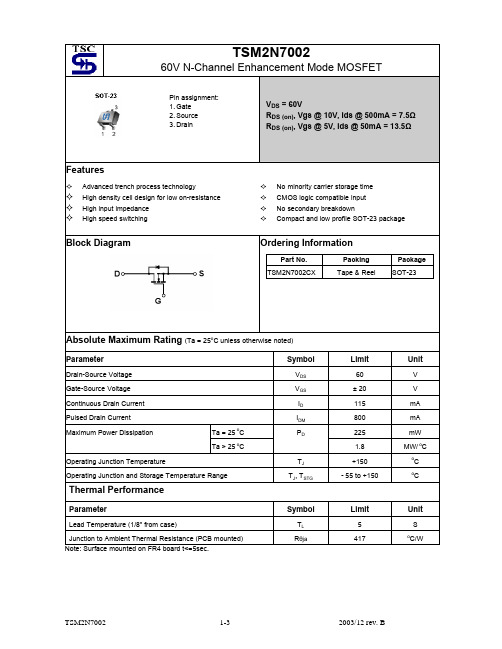
TSM2N700260V N-Channel Enhancement Mode MOSFETV DS = 60VR DS (on), Vgs @ 10V, Ids @ 500mA = 7.5ΩR DS (on), Vgs @ 5V, Ids @ 50mA = 13.5ΩFeaturesAdvanced trench process technologyHigh density cell design for low on-resistanceHigh input impedanceHigh speed switchingNo minority carrier storage timeCMOS logic compatible inputNosecondarybreakdownCompact and low profile SOT-23 packageBlock Diagram Ordering InformationPart No. Packing PackageTSM2N7002CX Tape&Reel SOT-23Absolute Maximum Rating (Ta = 25o C unless otherwise noted)Parameter SymbolLimitUnit Drain-Source Voltage V DS 60 VGate-Source Voltage V GS ±20 VContinuous Drain Current I D115 mAPulsed Drain Current I DM 800 mATa = 25 o C 225mWMaximum Power DissipationTa > 25 o CP D1.8 MW/ o COperating Junction Temperature T J +150 o COperating Junction and Storage Temperature Range T J, T STG- 55 to +150 o CThermal PerformanceParameter SymbolLimitUnit Lead Temperature (1/8” from case) T L 5 SJunction to Ambient Thermal Resistance (PCB mounted) Rθja 417 o C/WNote: Surface mounted on FR4 board t<=5sec.Pin assignment:1. Gate2. Source3. DrainElectrical CharacteristicsTj = 25 oC unless otherwise notedParameter Conditions Symbol Min Typ Max UnitStaticDrain-Source Breakdown Voltage V GS = 0V, I D = 10uA BV DSS 60 -- -- V Drain-Source On-State Resistance V GS = 10V, I D = 500mA R DS(ON) -- -- 7.5 Drain-Source On-State Resistance V GS = 5V, I D = 50mA R DS(ON) -- -- 13.5 Ω Gate Threshold Voltage V DS = V GS , I D = 250uA V GS(TH) 1.0-- 2.5 VZero Gate Voltage Drain Current V DS = 60V, V GS = 0V I DSS -- -- 1.0 uA Gate Body Leakage V GS = ± 20V, V DS = 0V I GSS -- -- ± 100 nA On-State Drain CurrentV DS 2V, V GS = 10VI D(ON) 500 -- -- mADynamicTurn-On Rise Time t r -- -- 20 Turn-Off Fall Time V DD = 25V, R L = 50Ω, I D = 500mA, V GEN = 10V, R G = 25Ωt f -- -- 40 nSInput Capacitance C iss -- 50 -- Output CapacitanceC oss -- 25 -- Reverse Transfer CapacitanceV DS = 25V, V GS = 0V, f = 1.0MHzC rss -- 5 --pF Source-Drain DiodeMax. Diode Forward CurrentI S -- -- 115 mA Diode Forward VoltageI S = 115mA, V GS = 0VV SD -- 1.3 1.5 VNote : pulse test: pulse width <=300uS, duty cycle <=2%。
2N7002KT1G中文资料

2N7002KSmall Signal MOSFET60 V, 380 mA, Single, N−Channel, SOT−23 Features•ESD Protected•Low R DS(on)•Surface Mount Package•This is a Pb−Free DeviceApplications•Low Side Load Switch•Level Shift Circuits•DC−DC Converter•Portable Applications i.e. DSC, PDA, Cell Phone, etc. MAXIMUM RATINGS (T J = 25°C unless otherwise stated)Rating Symbol Value Unit Drain−to−Source Voltage V DSS60V Gate−to−Source Voltage V GS±20VDrain Current (Note 1)Steady State T A = 25°CT A = 85°Ct < 5 s T A = 25°CT A = 85°C I D320230380270mAPower Dissipation (Note 1) Steady Statet < 5 s P D300420mWPulsed Drain Current (t p = 10 m s)I DM 1.5AOperating Junction and Storage Temperature Range T J, T STG−55 to+150°CSource Current (Body Diode)I S300mALead Temperature for Soldering Purposes (1/8″ from case for 10 s)TL260°CGate−Source ESD Rating(HBM, Method 3015)ESD2000VStresses exceeding Maximum Ratings may damage the device. Maximum Ratings are stress ratings only. Functional operation above the Recommended Operating Conditions is not implied. Extended exposure to stresses above the Recommended Operating Conditions may affect device reliability. THERMAL CHARACTERISTICSCharacteristic Symbol Max Unit Junction−to−Ambient − Steady State(Note1)R q JA417°C/W Junction−to−Ambient − t ≤ 5 s (Note 1)R q JA3001.Surface−mounted on FR4 board using 1 in sq pad size (Cu area = 1.127 insq [1 oz] including traces)Device Package Shipping†ORDERING INFORMATION2N7002KT1G3000/T ape & ReelSimplified SchematicSOT−23CASE 318STYLE 21704 M GGMARKING DIAGRAM& PIN ASSIGNMENT321DrainGate SourceSOT−23(Pb−Free)60 V 1.6 W @ 10 VR DS(on) MAX380 mAI D MAX(Note 1)V(BR)DSS†For information on tape and reel specifications, including part orientation and tape sizes, please refer to our T ape and Reel Packaging Specifications Brochure, BRD8011/D.2.5 W @ 4.5 VGateSourceDrain(Top View)704= Specific Device CodeM= Date CodeG= Pb−Free Package(Note: Microdot may be in either location) *Date Code orientation and/or position mayvary depending upon manufacturing location.ELECTRICAL CHARACTERISTICS (T J = 25°C unless otherwise specified)Parameter Symbol Test Condition Min Typ Max Units OFF CHARACTERISTICSDrain−to−Source Breakdown Voltage V(BR)DSS V GS = 0 V, I D = 250 m A60V Drain−to−Source Breakdown VoltageTemperature CoefficientV(BR)DSS/T J71mV/°CZero Gate Voltage Drain Current I DSS VGS = 0 V,V DS = 60 V T J = 25°C1m A T J = 125°C500V GS = 0 V,V DS = 50 VT J = 25°C100nA Gate−to−Source Leakage Current I GSS V DS = 0 V, V GS = ±20 V±10m AV DS = 0 V, V GS = ±10 V450nAV DS = 0 V, V GS = ±5.0 V150nA ON CHARACTERISTICS (Note 2)Gate Threshold Voltage V GS(TH)V GS = V DS, I D = 250 m A 1.0 2.5V Negative Threshold TemperatureCoefficientV GS(TH)/T J 4.0mV/°C Drain−to−Source On Resistance R DS(on)V GS = 10 V, I D = 500 mA 1.19 1.6WV GS = 4.5 V, I D = 200 mA 1.33 2.5Forward Transconductance g FS V DS = 5 V, I D = 200 mA80S CHARGES AND CAPACITANCESInput Capacitance C ISSV GS = 0 V, f = 1 MHz,V DS = 20 V 24.5pFOutput Capacitance C OSS 4.2 Reverse Transfer Capacitance C RSS 2.2Total Gate Charge Q G(TOT)V GS = 4.5 V, V DS = 10 V;I D = 200 mA 0.7nCThreshold Gate Charge Q G(TH)0.1 Gate−to−Source Charge Q GS0.3 Gate−to−Drain Charge Q GD0.1 SWITCHING CHARACTERISTICS, V GS = V (Note 3)Turn−On Delay Time t d(ON)V GS = 10 V, V DD = 25 V,I D = 500 mA, R G = 25 W 12.2nsRise Time t r9.0 Turn−Off Delay Time t d(OFF)55.8 Fall Time t f29 DRAIN−SOURCE DIODE CHARACTERISTICSForward Diode Voltage V SD VGS = 0 V,I S = 200 mA T J = 25°C0.8 1.2V T J = 85°C0.72.Pulse Test: pulse width ≤ 300 m s, duty cycle ≤ 2%3.Switching characteristics are independent of operating junction temperaturesFigure 1. On −Region CharacteristicsFigure 2. Transfer CharacteristicsV DS , DRAIN −TO −SOURCE VOLTAGE (V)V GS , GATE −TO −SOURCE VOLTAGE (V)Figure 3. On −Resistance vs. Drain Current andTemperatureFigure 4. On −Resistance vs. Drain Current andTemperatureI D , DRAIN CURRENT (A)Figure 5. On −Resistance vs. Gate −to −SourceVoltage Figure 6. On −Resistance Variation withTemperatureV GS , GATE −TO −SOURCE VOLTAGE (V)T J , JUNCTION TEMPERATURE (°C)I D , D R A I N C U R R E N T (A )I D , D R A I N C U R R E N T (A )R D S (o n ), D R A I N −T O −S O U R C E R E S I S T A N C E (W )R D S (o n ), D R A I N −T O −S O U R C E R E S I S T A N C E (W )R D S (o n ), D R A I N −T O −S O U R C E R E S I S T A N C E (N O R M A L I Z E D )I D , DRAIN CURRENT (A)R D S (o n ), D R A I N −T O −S O U R C E R E S I S T A N C E (W )Figure 7. Capacitance VariationFigure 8. Gate −to −Source andDrain −to −Source Voltage vs. Total ChargeQg, TOTAL GATE CHARGE (nC)Figure 9. Diode Forward Voltage vs. CurrentV SD , SOURCE −TO −DRAIN VOLTAGE (V)110V G S , G A T E −T O −S O U R C E V O L T A G E (V )I S , S O U R C E C U R R E N T (A )C , C A P A C I T A N C E (p F )GATE −TO −SOURCE OR DRAIN −TO −SOURCE VOLTAGE (V)0.1PACKAGE DIMENSIONSSOT −23 (TO −236)CASE 318−08ISSUE ANSTYLE 21:PIN 1.GATE2.SOURCE3.DRAINNOTES:1.DIMENSIONING AND TOLERANCING PER ANSI Y14.5M, 1982.2.CONTROLLING DIMENSION: INCH.3.MAXIMUM LEAD THICKNESS INCLUDES LEAD FINISHTHICKNESS. MINIMUM LEAD THICKNESS IS THE MINIMUM THICKNESS OF BASE MATERIAL.4.318−01 THRU −07 AND −09 OBSOLETE, NEW STANDARD 318−08.SOLDERING FOOTPRINTVIEW CDIM A MIN NOM MAX MINMILLIMETERS0.89 1.00 1.110.035INCHES A10.010.060.100.001b 0.370.440.500.015c 0.090.130.180.003D 2.80 2.90 3.040.110E 1.20 1.30 1.400.047e 1.78 1.90 2.040.070L 0.100.200.300.0040.0400.0440.0020.0040.0180.0200.0050.0070.1140.1200.0510.0550.0750.0810.0080.012NOM MAX L1 2.102.40 2.640.0830.0940.104H E0.350.540.690.0140.0210.029ON Semiconductor and are registered trademarks of Semiconductor Components Industries, LLC (SCILLC). SCILLC reserves the right to make changes without further noticeto any products herein. SCILLC makes no warranty, representation or guarantee regarding the suitability of its products for any particular purpose, nor does SCILLC assume any liability arising out of the application or use of any product or circuit, and specifically disclaims any and all liability, including without limitation special, consequential or incidental damages.“Typical” parameters which may be provided in SCILLC data sheets and/or specifications can and do vary in different applications and actual performance may vary over time. All operating parameters, including “Typicals” must be validated for each customer application by customer’s technical experts. SCILLC does not convey any license under its patent rights nor the rights of others. SCILLC products are not designed, intended, or authorized for use as components in systems intended for surgical implant into the body, or other applications intended to support or sustain life, or for any other application in which the failure of the SCILLC product could create a situation where personal injury or death may occur. Should Buyer purchase or use SCILLC products for any such unintended or unauthorized application, Buyer shall indemnify and hold SCILLC and its officers, employees, subsidiaries, affiliates,and distributors harmless against all claims, costs, damages, and expenses, and reasonable attorney fees arising out of, directly or indirectly, any claim of personal injury or death associated with such unintended or unauthorized use, even if such claim alleges that SCILLC was negligent regarding the design or manufacture of the part. SCILLC is an Equal Opportunity/Affirmative Action Employer. This literature is subject to all applicable copyright laws and is not for resale in any manner.PUBLICATION ORDERING INFORMATION。
2N7002中文资料(Diodes)中文数据手册「EasyDatasheet - 矽搜」
反向传输电容
(2)
C
5
pF
导通时间(2)(3)
t
关闭时间(2)(3)
t
20 ns V 30V, I =200mA 20 ns R =25Ω, R =150Ω
(1)脉冲条件下进行测定.宽度=300μS.占空比 (3)开关时间测量50Ω源阻抗和5ns上升时间脉冲发生器
辣妹参数数据可应要求提供该设备
2% (2)抽样检测.
门 - 体泄漏
零栅压漏 当前
I
10 nA V =± 20V, V =0V
I
1
µA V =48V, V =0V
500 µA V =48V, V =0V, T=125°C (2)
通态漏电流(1)
I
500
mA V =25V, V =10V
静态漏源通态
电压(1)
V
3.75 V V =10V, I =500mA
芯片中文手册,看全文,戳
SOT23 N沟道增强 模式垂直DMOS FET
ISSUE 4 – 2006年 4月
特征
* 60电压V CEO
PARTMARKING详细信息 - 702
2N7002
S D
G
绝对最大额定值.
SOT23
参数
符号
VALUE
UNIT
漏源电压
V
60
V
连续漏极电流在T
=25°C
I
115
mA
漏电流脉冲
I
800
mA
门源电压
V
± 40
V
在T功率耗散
=25°C
P
330
mW
工作和存储温度范围
T :T
2N7002-AE3-R资料

UNISONIC TECHNOLOGIES CO.,2N7002MOSFETN-CHANNEL ENHANCEMENT MODE FIELD EFFECT TRANSISTORDESCRIPTIONThe UTC 2N7002 has been designed to minimize on-state resistance while provide rugged, reliable, and fast switching performance. It can be used in most applications requiring up to 400mA DC and can deliver pulsed currents up to 2A. The product is particularly suited for low voltage, low current applications such as small servo motor control, power MOSFET gate drivers, and other switching applicationsFEATURES* High density cell design for low R DS(ON). * Voltage controlled small signal switch * Rugged and reliable * High saturation current capabilityMARKING*Pb-free plating product number: 2N7002LPIN CONFIGURATIONPIN NO.PIN NAME1 SOURCE2 GATE3 DRAINORDERING INFORMATIONOrder NumberNormal Lead free Package Packing2N7002-AE3-R 2N7002L-AE3-R SOT-23 Tape ReelABSOLUTE MAXIMUM RATINGS (Ta=25°C unless otherwise noted.)PARAMETER SYMBOL RATINGS UNITDrain-Source Voltage V DSS 60 V Drain-Gate Voltage (R GS ≤1M Ω) V DGR 60 V Continuous ±20Gate Source Voltage Non Repetitive(tp<50µs)V GSS±40 V Continuous 115Maximum Drain Current Pulsed I D 800mA Maximum Power DissipationDerated above 25°CP D200 1.6 mW mW/°C Operating Temperature T OPR 0 ~ +70 °CStorage Temperature T STG -40 ~ +150THERMAL CHARACTERISTICSPARAMETER SYMBOL RATINGS UNITThermal Resistance, Junction to Ambient θJA 625 °C/WELECTRICAL CHARACTERISTICS (T A =25°C, unless otherwise specified.)PARAMETER SYMBOL TEST CONDITIONS MIN TYP MAX UNIT OFF CHARACTERISTICSDrain-Source Breakdown Voltage BV DSS V GS =0V, I D =10µA 60 V0.5 mAZero Gate Voltage Drain Current I DSSV DS =60V, V GS =0V T J =125°C 1 µAGate-Body leakage, Forward I GSSF V GS =20V, V DS =0V 100 nA Gate-Body leakage Reverse I GSSR V GS =-20V, V DS =0V -100nA ON CHARACTERISTICS (Note) Gate Threshold Voltage V GS (th) V GS = V DS , I D =250µA 1 2.1 2.5 VV GS = 10V, I D =500mA 0.6 3.75Drain-Source On-Voltage V DS (ON) V GS = 5.0V, I D =50mA 0.09 1.5VOn-State Drain Current I D(ON) V GS =10V,V DS ≥2V DS(ON) 500 2700 mAV GS =10V, I D =500mAT J =100°C1.2 1.7 7.5 13.5Ω Static Drain-Source On-Resistance R DS (ON)V GS =5.0V, I D =50mAT J =100°C1.72.4 7.5 13.5 Forward Transconductance g FS V DS ≥2V DS(ON), I D =200mA 80 320 mS DYNAMIC CHARACTERISTICS Input Capacitance C iss V DS =25V,V GS =0V,f =1.0MHz 20 50 pF Output Capacitance C oss 11 25 pF Reverse Transfer Capacitance C rss 4 5 pFTurn-On Time t ONV DD =30V, R L =150ΩI D =200mA, V GS =10V R GEN =25Ω20 nS Turn-Off Time t OFFV DD =30V, R L =25ΩI D =200mA, V GS =10V R GEN =25Ω20 nS DRAIN-SOURCE DIODE CHARACTERISTICS AND MAXIMUM RATINGS Drain-Source Diode Forward Voltage V SD V GS =0V, Is=115mA (Note ) 0.88 1.5 VMaximum Pulsed Drain-Source DiodeForward CurrentI SM 0.8 AMaximum Continuous Drain-SourceDiode Forward CurrentIs 115 mANote: Pulse Test: Pulse Width ≤300µs, Duty Cycle ≤2.0%TEST CIRCUIT AND WAVEFORMFigure 1V DDV OUTFigure 2. Switching WaveformsTYPICAL CHARACTERICS543211.510.50221.61.20.80.432.521.5100.5D R A I N -S O U R CE C U R R E N T , I D (A )DRAIN -SOURCE VOLTAGE, V DS (V)Figure 3. On-Region CharacteristicsN O R M A L I Z E D D R A I N –S O U R C E O N –R E S I S T A N C E , R D S (O N )DRAIN CURRENT , I D (A)Figure 4. On-Resistance Varisation with GateVoltage and Drain Current100750-2521.51-500.51.61.20.80.432.521.5100.525501501250.751.251.7520N O R M A L I Z E D D R A I N -S O U R C E O N -R E S I S T A N C E , R D S (O N )JUCTION TEMPERATURE, T J (°C)Figure 5. On-Resistance Varisationwith TemperatureN O R M A L I Z E D D R A I N -S O U R C E O N -R E S I S T A N C E , R DS (O N )DRAIN CURRENT ,I D (A)Figure 6. On-Resistance Varisation with DrainCurrent and Temperature10864210075-25-5025501251.61.21.80.4201501.11.0510.950.90.850.8D R A I N C U R R E N T , I D (A )GATE TO SOURCE VOLTAGE , V GS (V)Figure 7. Transfer CharacteristicsN O R M A L I Z E D G A T E -S O U R C E T H R E S H O L D V O L T A G E , V t hJUCTION TEMPERATURE, T J (°C)Figure 8. Gate Threshold Varisationwith TemperatureTYPICAL CHARACTERICS (cont.)10075-251.11.051-500.9251 1.20.80.410.50.10.050.010.20.00525501501250.951.0251.0751.40.0010.9750.62N O R M A L I Z E D D R A I N -S O U R C E V R E A K D O W N V O L T A G E , B V D S SJUCTION TEMPERATURE, T J (°C)Figure 9. Breakdown Voltage Varisationwith TemperatureBODY DIODE FORWARD VOLTAGE , V SD (V)Figure 10. Body Diode Forward Voltage Varisationwith TemperatureR E V E R S E D R A I N C U R R E N T , I S (A )1102053220.80.41.21.6205102401503060C A P A C I T A N C E (p F )DRAIN TO SOURCE VOLTAGE, V DS (V)Figure 11. Capacitance CharacteristicsGATE CHARGE, Qg (nC)Figure 12. Gate Charge Characteristics60801020520.50.050.10.0110.00530231D R A I N C U R RE N T , I D (A )DRAIN TO SOURCE VOLTAGE, V DS (V)Figure 13. Maximum Safe Operating Area3000.001101t1, TIME (sec)10010.10.010.0010.00010.0020.010.050.10.20.5Figure 14. Transient Thermal Response CurveN O R M A L I Z E D E F F E C T I V E T R A N S I E N T T H E R M A L R E S I S T A N C E , r (t )。
2N7002VC-7资料
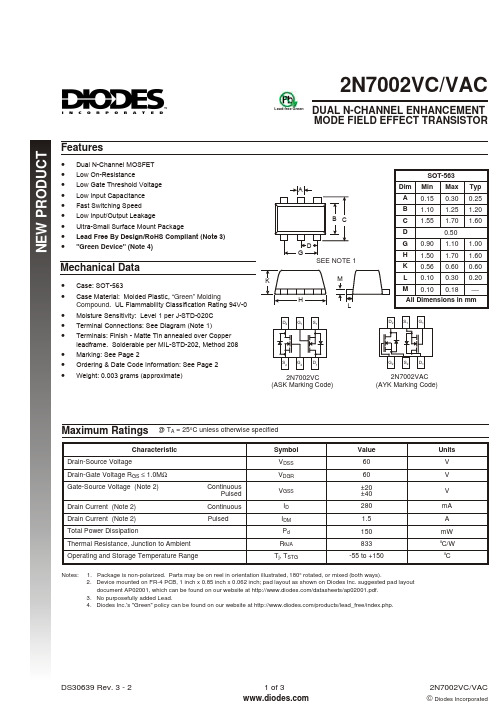
SOT-563 Dim A B C D G H SEE NOTE 1
K H M
Min 0.15 1.10 1.55 0.90 1.50 0.56 0.10 0.10
Max 0.30 1.25 1.70 0.50 1.10 1.70 0.60 0.30 0.18
Typ 0.25 1.20 1.60 1.00 1.60 0.60 0.20
Characteristic Drain-Gate Voltage RGS ≤ 1.0MΩ Gate-Source Voltage (Note 2) Drain Current (Note 2) Drain Current (Note 2) Total Power Dissipation Thermal Resistance, Junction to Ambient Operating and Storage Temperature Range
D2
S1
G1
ห้องสมุดไป่ตู้
AYK YM
G2 S2 D1
AYK = 2N7002VAC Product Type Marking Code (See Note 1) YM = Date Code Marking Y = Year ex: R = 2004 M = Month ex: 9 = September
Date Code Key Year Code Month Code Jan 1 Feb 2 March 3 Apr 4 May 5 Jun 6 2004 R Jul 7 2005 S Aug 8 2006 T Sep 9 2007 U Oct O 2008 V Nov N 2009 W Dec D
DS30639 Rev. 3 - 2
2N7002

SOT-23 封装半导体场效应管/SOT-23 Plastic-Encapsulate MOSFETS
2N7002 MOSFET( N-Channel )
印章/MARKING: 7002 特点/Features:
1、控制触发灵敏; 2、维持电流低; 用途/Applications: 用于一般开关和相位电路。
1.2 V
50 pF
25
20 ns
40 ns
400
ns
Tstg
-55~150
℃
电性能参数/Electrical characteristics (Ta=25℃)
参数
符号
测试条件
最小值 典型值 最大值 单位
源极-漏极击穿电压 栅极开启电压 栅极漏电流
零栅压漏极电流 漏极导通电流
漏极源极导通电阻
正向跨导
漏极-源极导通电压
二极管正向压降 输入电容 输出电容 开启时间 关闭时间
SOT-23
1.GATE 2.SOURCE 3.DRAIN
极限参数/Absolute maximum ratings(Ta=25℃)
参数/Parameter
符号/ Symbol 数值/Value 单位/Unit
源极-漏极电压/Drai流(持续)/Continuous Drain Current
ID
耗散功率/Power Dissipation
PD
热阻/ Thermal Resistance Junction to Ambient
RθJA
结温/Junction Temperature
Tj
60 0.115 0.225 556 150
V A W ℃/mW ℃
储存温度/Storage Temperature
2n7002耗散功率

2n7002耗散功率2n7002是一种常见的场效应管,广泛应用于电子设备中。
耗散功率是指器件在工作过程中所消耗的功率,对于2n7002而言,耗散功率是一个重要的参数。
首先,我们来了解一下2n7002的基本特性。
2n7002是一种N沟道增强型场效应管,具有低电压驱动、低电流驱动和高开关速度等特点。
它的主要用途是作为开关管,用于控制电路的通断。
在电子设备中,2n7002常用于电源管理、电流控制、信号放大等方面。
对于2n7002而言,耗散功率是一个重要的参数。
耗散功率的大小直接影响到器件的工作温度和可靠性。
在正常工作状态下,2n7002的耗散功率应该在一定范围内,以保证器件的正常工作和长寿命。
那么,如何计算2n7002的耗散功率呢?首先,我们需要知道2n7002的工作电压和工作电流。
工作电压是指2n7002在工作过程中的电压,通常为正常工作电压和最大工作电压。
工作电流是指2n7002在工作过程中的电流,通常为正常工作电流和最大工作电流。
在计算耗散功率时,我们可以使用以下公式:耗散功率 = 工作电压×工作电流。
根据实际情况,我们可以选择正常工作电压和正常工作电流进行计算,以保证器件的正常工作。
除了计算耗散功率,我们还需要关注2n7002的散热问题。
由于耗散功率的存在,2n7002会产生一定的热量。
如果散热不良,会导致器件温度过高,从而影响器件的性能和寿命。
因此,在设计电路时,我们需要考虑散热措施,如合理布局散热片、增加散热风扇等,以保证2n7002的正常工作温度。
总之,2n7002的耗散功率是一个重要的参数,直接影响到器件的工作温度和可靠性。
在使用2n7002时,我们需要合理计算耗散功率,并采取相应的散热措施,以保证器件的正常工作和长寿命。
只有这样,我们才能充分发挥2n7002的性能,为电子设备的正常运行提供保障。
2N7002中文资料_数据手册_参数
2N7002P_1本文档提供的所有信息均受法律免责声明保护. ?恩智浦BV 2010.保留所有权利.产品数据表 2010年4月1日至19日 14 16恩智浦 半导体 2N7002P 60 V,0.3 A N沟道沟槽式MOSFET 12.法律信息 12.1数据表状态 [1]请在启动或完成设计之前查阅近发布的文档. [2]术 语“短数据表”在“定义”一节中进行了说明. [3]本文档中描述的设备的产品状态可能在本文档发布后发生变化,并且在多个设备 的情况下可能会有所不同.新的产品状态 有关信息可以在网址上找到 . 12.2定义草案 - 文件仅为草案版本.内容还在内部审查和正式批 准,可能会导致修改或添加.恩智浦半导体不给任何陈述或保证的准确性或完整性信息包括在内,对后果不承担任何责任使用这些信 息.简短的数据表 - 简短的数据表是完整数据表的摘要具有相同的产品型号和标题.一个简短的数据表是打算仅供快速参考,不应依赖 于详细说明完整的信息.有关详细和完整的信息,请参阅相关的完整数据可通过当地恩智浦半导体销售部门索取办公室.如果与短数 据表有任何不一致或冲突,应以完整的数据表为准.产品规格 - 产品中提供的信息和数据数据表应按照约定的方式定义产品的规格恩 智浦半导体及其客户,除非恩智浦半导体和客户已经以书面形式明确表示同意.然而,在任何情况下,恩智浦半导体产品的协议应是 有效的被视为提供了超出上述范围之外的功能和品质产品数据表. 12.3免责声明有限保修和责任 - 本文件中的信息被认为是准确可靠. 但是,恩智浦半导体并没有给予任何陈述或保证,明示或暗示,准确性或这些信息的完整性,对此不承担任何责任使用这些信息的 后果.恩智浦半导体不对任何间接的,附带的,惩罚性的,特殊的或相应的损害赔偿(包括但不限于 - 损失利润,储蓄损失,业务中 断,与搬迁有关的费用更换任何产品或返工费用)是否这样损害赔偿是基于侵权(包括疏忽),保修,违约 恩智浦BV 2010.保留所有权利.产品数据表 2010年4月1日至19日 13的16恩智浦半导体 2N7002P 60 V,0.3 A N沟道沟槽式MOSFET 11.修 订历史表8修订记录文档ID发布日期数据表状态变更通知取代版本 2N7002P_1 20100419产品数据表日至19日十六恩智浦半导体 2N7002P 60 V,0.3 A N沟道沟槽式MOSFET 8.测试信息图17.占空比定义 T 1 T 2 P ? 006AAA812占空比 δ= T 1 T 2 N沟道增强型场效应晶体管(FET)采用塑料封装 TRENCHMOS技术. 1.2特点 1.3应用 1.4快速参考数据 2.固定信息 2N7002F N沟道 TRENCHMOS FET 2006年4月3 - 28日产品数据表 逻辑电平阈值兼容 非常快速的切换 S 表面安装的包装 S的 TRENCHMOS技术 S 逻辑 电平转换器 S 的高速线路驱动器 S V DS≤60 V S I D≤475 MA S R DSON≤2Ω S P TOT≤0.83 W表格1:钢钉销描述简化的轮廓符号 1 门(G) SOT23 2来源(S) 3排水(D) 12 3小号 D G MBB076
2N7002MTF_NL资料
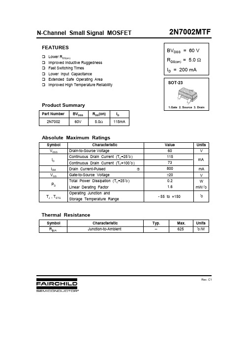
ACEx™ FAST ActiveArray™ FASTr™ Bottomless™ FPS™ CoolFET™ FRFET™ CROSSVOLT™ GlobalOptoisolator™ DOME™ GTO™ EcoSPARK™ HiSeC™ E2CMOS™ I2C™ EnSigna™ i-Lo™ FACT™ ImpliedDisconnect™ FACT Quiet Series™
Rev. C1
元器件交易网
2N7002MTF
Symbol BVDSS VGS(th) IGSS Characteristic Drain-Source Breakdown Voltage Gate Threshold Voltage Gate-Source Leakage, Forward Gate-Source Leakage, Reverse Min. 60 1.2 IDSS ID(ON) RDS(on) gfs Ciss Coss Crss td(on) tr td(off) tf Drain-to-Source Leakage Current On-State Drain-Source Current Static Drain-Source On-State Resistance ② 0.5 0.08 500 5.0 50 25 5 20 20 ns pF A Ω S Typ. -
N-Channel Small Signal MOSFET
Electrical Characteristics (TC=25℃ unless otherwise specified)
Max. Units 2.5 100 nA -100 1.0 µA V V Test Condition VGS = 0V, ID = 250µA VDS = VGS, ID = 250µA VGS = 20V VGS = -20V VGS = 40V VGS = 40V, TC = 125℃ VDS = 10V, VGS = 10V VGS = 10V, ID = 0.5A VDS = 15V, ID = 0.2A VDS = 25V, VGS = 0V, f = 1.0MHz
2N7002DW-TP;中文规格书,Datasheet资料
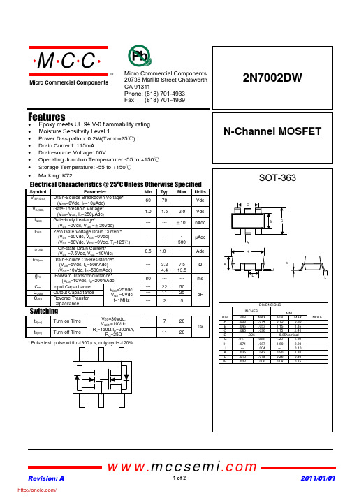
NOTE
* Pulse test, pulse width̰300s, duty cyclḛ20%
Revision: A
/
1 of 2
2011/01/01
MCC
TM
Micro Commercial Components
Ordering Information :
/
2 of 2
Revision: A
2011/01/01
分销商库存信息:
MICRO-COMMERICAL-CO 2N7002DW-TP
MCC
Micro Commercial Co 20736 Marilla Street Chatsworth !"# $
% !"#
2N7002DW
Switching
td(on) td(off) Turn-on Time Turn-off Time ----7 11 20 ns 20
DIM A B C D G H J K L M
MIN .006 .045 .085 .026 .047 .071 --.035 .010 .003
MAX .014 .053 .096 .055 .087 .004 .043 .018 .006
• • • • • • • •
Features
Epoxy meets UL 94 V-0 flammability rating Moisture Sensitivity Level 1 Power Dissipation: 0.2W(Tamb=25ć) Drain Current: 115mA Drain-source Voltage: 60V Operating Junction Temperature: -55 to +150к Storage Temperature: -55 to +150к Marking: K72
2n7002工作原理
2n7002工作原理2n7002是一种N沟道MOSFET晶体管,它是一种常用的低功耗开关器件。
在电子设备中,2n7002被广泛应用于电源管理、电路保护、信号放大和信号开关等领域。
本文将介绍2n7002的工作原理及其应用。
2n7002的工作原理2n7002是一种N沟道MOSFET晶体管,它由源极、漏极和栅极三个电极组成。
当栅极施加正电压时,栅极和源极之间形成一个电场,使得N型沟道中的电子被吸引到栅极附近,从而形成一个导电通道。
这个导电通道连接了源极和漏极,使得电流可以从源极流入漏极。
当栅极施加负电压时,栅极和源极之间的电场被抑制,导电通道被关闭,电流无法从源极流入漏极。
2n7002的应用2n7002是一种常用的低功耗开关器件,它可以用于电源管理、电路保护、信号放大和信号开关等领域。
下面将分别介绍2n7002在这些领域的应用。
1. 电源管理在电源管理中,2n7002通常用于电源开关。
当栅极施加正电压时,2n7002导通,电源输出电压可以传递到负载上;当栅极施加负电压时,2n7002截止,电源输出电压无法传递到负载上。
这样可以实现对电源的控制,从而达到节能的目的。
2. 电路保护在电路保护中,2n7002通常用于过压保护和过流保护。
当电路中出现过压或过流时,2n7002可以通过控制电路的开关状态来保护电路。
例如,在过压保护中,当电路中出现过压时,2n7002可以通过截止来防止过压对电路造成损害。
3. 信号放大在信号放大中,2n7002通常用于放大小信号。
当小信号施加到栅极上时,2n7002可以将小信号放大到较大的电压范围内,从而实现信号放大的目的。
这样可以提高信号的质量和稳定性,从而提高电路的性能。
4. 信号开关在信号开关中,2n7002通常用于控制信号的开关状态。
例如,在音频放大器中,2n7002可以通过控制音频信号的开关状态来实现音频信号的放大和静音。
这样可以提高音频信号的质量和稳定性,从而提高音频放大器的性能。
FOSAN富信电子 MOS管 2N7002-产品规格书
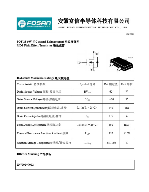
安徽富信半导体科技有限公司ANHUI FOSAN SEMICONDUCTOR TECHNOLOGY CO.,LTD.2N7002 SOT-2360V N Channel Enhancement沟道增强型MOS Field Effect Transistor场效应管▉Absolute Maximum Ratings最大额定值Characteristic特性参数Symbol符号Rat额定值Unit单位Drain-Source V oltage漏极-源极电压BV DSS60V Gate-Source Voltage栅极-源极电压V GS+20V Drain Current(continuous)漏极电流-连续I D(at T A=25°C)340mA Drain Current(pulsed)漏极电流-脉冲I DM 1.5A Total Device Dissipation总耗散功率P D(at T A=25°C)350mW Thermal Resistance Junction-Ambient热阻RΘJA357℃/W Junction/Storage Temperature结温/储存温度T J,T stg-55~150℃▉Device Marking产品字标2N7002=7002ANHUI FOSAN SEMICONDUCTOR TECHNOLOGY CO.,LTD.2N7002▉Electrical Characteristics电特性(T A=25℃unless otherwise noted如无特殊说明,温度为25℃)Characteristic 特性参数Symbol符号Min最小值Typ典型值Max最大值Unit单位Drain-Source Breakdown Voltage漏极-源极击穿电压(I D=250uA,V GS=0V)BV DSS60——VGate Threshold Voltage栅极开启电压(I D=250uA,V GS=V DS)V GS(th)1 1.5 2.5VZero Gate Voltage Drain Current零栅压漏极电流(V GS=0V,V DS=60V)I DSS——1u AGate Body Leakage栅极漏电流(V GS=+20V,V DS=0V)I GSS——+100n AStatic Drain-Source On-State Resistance 静态漏源导通电阻(I D=300mA,V GS=10V) (I D=200mA,V GS=4.5V)R DS(ON)— 1.21.32.53.0ΩDiode Forward Voltage Drop内附二极管正向压降(I SD=300mA,V GS=0V)V SD—— 1.2V Input Capacitance输入电容(V GS=0V,V DS=30V,f=1MHz)C ISS—27.5—pF Common Source Output Capacitance共源输出电容(V GS=0V,V DS=30V,f=1MHz)C OSS— 2.75—pF Reverse Transfer Capacitance反馈电容(V GS=0V,V DS=30V,f=1MHz)C RSS— 1.9—pF Total Gate Charge栅极电荷密度(V DS=30V,I D=300mA,V GS=10V)Q g— 1.6—nC Gate Source Charge栅源电荷密度(V DS=30V,I D=300mA,V GS=10V)Q gs—0.47—nC Gate Drain Charge栅漏电荷密度(V DS=30V,I D=300mA,V GS=10V)Q gd—0.25—nC Turn-ON Delay Time开启延迟时间(V DS=30V I D=300mA,R GEN=6Ω,V GS=10V)t d(on)— 3.3—ns Turn-ON Rise Time开启上升时间(V DS=30V I D=300mA,R GEN=6Ω,V GS=10V)t r—19—ns Turn-OFF Delay Time关断延迟时间(V DS=30V I D=300mA,R GEN=6Ω,V GS=10V)t d(off)—9.6—ns Turn-OFF Fall Time关断下降时间(V DS=30V I D=300mA,R GEN=6Ω,V GS=10V)t f—49—nsANHUI FOSAN SEMICONDUCTOR TECHNOLOGY CO.,LTD.2N7002■Typical Characteristic Curve典型特性曲线Figure1:Output Characteristics Figure2:Transfer CharacteristicsFigure3:On-Resistance vs.Drain Current Figure4:Safe Operating AreaFigure5:Capacitance Characteristics Figure6:Gate-Charge Characteristics安徽富信半导体科技有限公司ANHUI FOSAN SEMICONDUCTOR TECHNOLOGY CO.,LTD.2N7002▉Dimension外形封裝尺寸Symbol Dimensions In Millimeters Dimensions In Inches Min Max Min Max A 0.900 1.1500.0350.045A10.0000.1000.0000.004A20.900 1.0500.0350.041b 0.3000.5000.0120.020c 0.0800.1500.0030.006D 2.800 3.0000.1100.118E 1.200 1.4000.0500.055E1 2.2502.5500.0890.100e 0.950TYP0.037TYPe1 1.8002.0000.0710.079L 0.550REF0.022REFL10.3000.5000.0120.020θ0o8o 0o8o。
MEMORY存储芯片2N7002中文规格书

2N7000 / 2N7002 / NDS7002A N-Channel Enhancement Mode Field Effect Transistor
D
D
S
G
1
TO-92
G
SOT-23
1. Source 2. Gate 3. Drain
(TO-236AB)
S
2N7002/NDS7002A
Ordering Information
Part Number
2N7000 2N7000-D74Z 2N7000-D75Z 2N7000-D26Z
2N7002 NDS7002A
Absolute Maximum Ratings
Stresses exceeding the absolute maximum ratings may damage the device. The device may not function or be operable above the recommended operating conditions and stressing the parts to these levels is not recommended. In addition, extended exposure to stresses above the recommended operating conditions may affect device reliability. The absolute maximum ratings are stress ratings only. Values are at TC = 25°C unless otherwise noted.
2N7002DW;中文规格书,Datasheet资料
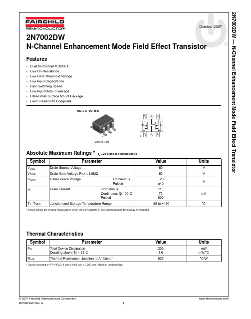
2N7002DW — N-Channel Enhancement Mode Field Effect Transistor 1Marking : 2N12N7002DW — N-Channel Enhancement Mode Field Effect TransistorElectrical Characteristics T C= 25°C unless otherwise notedOff Characteristics (Note1)On Characteristics (Note1)Dynamic CharacteristicsSwitching CharacteristicsNote1 : Short duration test pulse used to minimize self-heating effect .Symbol Parameter Test Condition MIN TYP MAX UnitsBV DSS Drain-Source Breakdown Voltage V GS = 0V, I D =10uA6078-V I DSS Zero Gate Voltage Drain Current V DS = 60V, V GS = 0VV DS = 60V, V GS = 0V, @T C = 125°C -0.0017 1.0500uA I GSSGate-Body LeakageV GS = ±20V, V DS = 0V-0.2±10nAV GS(th)Gate Threshold VoltageV DS = V GS , I D = 250uA1.0 1.762.0V R DS(ON)Satic Drain-Source On-Resistance V GS = 5V, I D = 0.05A,V GS = 10V, I D = 0.5A, @T j = 125°C -- 1.62.537.513.5ΩI D(ON)On-State Drain Current V GS = 10V, V DS = 7.5V 0.5 1.43-A g FSForward TransconductanceV DS = 10V, I D = 0.2A80356.5-mSC iss Input Capacitance V DS = 25V, V GS = 0V, f = 1.0MHz-37.850pF C oss Output Capacitance-12.425pF C rssReverse Transfer Capacitance- 6.57.0pFt D(ON)Turn-On Delay Time V DD = 30V, I D = 0.2A, V GEN = 10V R L = 150Ω, R GEN = 25Ω- 5.8520nst D(OFF)Turn-Off Delay Time-12.5202N7002DW — N-Channel Enhancement Mode Field Effect Transistor2N7002DW — N-Channel Enhancement Mode Field Effect Transistor2N7002DW — N-Channel Enhancement Mode Field Effect TransistorTRADEMARKSThe following are registered and unregistered trademarks and service marks Fairchild Semiconductor owns or is authorized to use andis not intended to be an exhaustive list of all such trademarks.DISCLAIMERFAIRCHILD SEMICONDUCTOR RESERVES THE RIGHT TO MAKE CHANGES WITHOUT FURTHER NOTICE TO ANY PRODUCTS HEREIN TO IMPROVE RELIABILITY, FUNCTION, OR DESIGN. FAIRCHILD DOES NOT ASSUME ANY LIABILITY ARISING OUT OFTHE APPLICATION OR USE OF ANY PRODUCT OR CIRCUIT DESCRIBED HEREIN; NEITHER DOES IT CONVEY ANY LICENSE UNDER ITS PATENT RIGHTS, NOR THE RIGHTS OF OTHERS. THESE SPECIFICATIONS DO NOT EXPAND THE TERMS OF FAIRCHILD’S WORLDWIDE TERMS AND CONDITIONS, SPECIFICALLY THE WARRANTY THEREIN, WHICH COVERS THESE PRODUCTS.LIFE SUPPORT POLICYFAIRCHILD’S PRODUCTS ARE NOT AUTHORIZED FOR USE AS CRITICAL COMPONENTS IN LIFE SUPPORT DEVICES OR SYSTEMS WITHOUT THE EXPRESS WRITTEN APPROVAL OF FAIRCHILD SEMICONDUCTOR CORPORATION.As used herein:1. Life support devices or systems are devices or systemswhich, (a) are intended for surgical implant into the body, or(b) support or sustain life, and (c) whose failure to performwhen properly used in accordance with instructions for useprovided in the labeling, can be reasonably expected to resultin significant injury to the user.2. A critical component is any component of a life supportdevice or system whose failure to perform can be reasonablyexpected to cause the failure of the life support device orsystem, or to affect its safety or effectiveness.PRODUCT STATUS DEFINITIONSDefinition of TermsACEx®Build it Now™CorePLUS™CROSSVOLT™CTL™Current Transfer Logic™EcoSPARK®Fairchild®Fairchild Semiconductor®FACT Quiet Series™FACT®FAST®FastvCore™FPS™FRFET®Global Power Resource SMGreen FPS™Green FPS™ e-Series™GTO™i-Lo™IntelliMAX™ISOPLANAR™MegaBuck™MICROCOUPLER™MicroFET™MicroPak™Motion-SPM™OPTOLOGIC®OPTOPLANAR®®PDP-SPM™Power220®Power247®POWEREDGE®Power-SPM™PowerTrench®Programmable Active Droop™QFET®QS™QT Optoelectronics™Quiet Series™RapidConfigure™SMART START™SPM®STEALTH™SuperFET™SuperSOT™-3SuperSOT™-6SuperSOT™-8SyncFET™The Power Franchise®TinyBoost™TinyBuck™TinyLogic®TINYOPTO™TinyPower™TinyPWM™TinyWire™µSerDes™UHC®UniFET™VCX™Datasheet Identification Product Status DefinitionAdvance Information Formative or In DesignThis datasheet contains the design specifications for product development.Specifications may change in any manner without notice.Preliminary First ProductionThis datasheet contains preliminary data; supplementary data will be pub-lished at a later date. Fairchild Semiconductor reserves the right to makechanges at any time without notice to improve design.No Identification Needed Full ProductionThis datasheet contains final specifications. Fairchild Semiconductor reservesthe right to make changes at any time without notice to improve design.Obsolete Not In ProductionThis datasheet contains specifications on a product that has been discontin-ued by Fairchild semiconductor. The datasheet is printed for reference infor-mation only.Rev. I302N7002DW N-Channel Enhancement Mode Field Effect Transistor 2N7002DW分销商库存信息: FAIRCHILD2N7002DW。
2N7002中文资料_数据手册_参数

件编号:71333 S09-0857-REV. E,2009年5月18日 VISHAY SILICONIX 2N7002K典型征 25°C,除非另有说明源极 - 漏极二极管正向电压温度阈值电 压方差 1.2 1.5 1 100 1000 0.0 0.3 0.6 0.9 T J = 125℃ V SD - 源极至漏极电压(V) 10 T J = - 55℃ V GS = 0V T J = 25℃ - 0.8 - 0.6 - 0.4 - 0.2 0.0 0.2 0.4 - 50 - 25 0 25 50 75 100 125 150 I D = 250μA T J - 结温(°C)导通电阻与栅源电压的关系单脉冲功率,结到环境 0 1 2 3 4五 02468 10 V GS - 栅极 - 源极电压(V) 我 D = 500毫安 我 D = 200毫安 0.01 0 1 2.5 3 100 600 0.1时间(S) 1.5 2 0.5 1 10 T A = 25℃归一化热暂态阻抗,结到环境 10 10 -3 10 -2 1 10 600 10 -1 -4 100 2 1 0.1 0.01 0.2 0.1 0.05 0.02单脉冲占空比= 0.5方波脉冲持续时间(S) 1.工作周期D = 2.每单位基数= R THJA = 350℃/ W 3. T JM - T A = P DM Z THJA(T) T 1 T 2 T 1 T 2笔记: 4.表面安装 P D
万联芯城
万联芯城-电子元器件采购网,专 为终端工厂客户提供一站式电子元器件配套服务,万 联芯城所售电子元器件均为原装现货库存,提交 BOM 表立即报价。万联芯城代理长电,顺络,先科 ST 等知名电子元器件品牌,价格有明显的优势,欢 迎广大客户咨询相关采购业务。点击进入万联芯城。
- 1、下载文档前请自行甄别文档内容的完整性,平台不提供额外的编辑、内容补充、找答案等附加服务。
- 2、"仅部分预览"的文档,不可在线预览部分如存在完整性等问题,可反馈申请退款(可完整预览的文档不适用该条件!)。
- 3、如文档侵犯您的权益,请联系客服反馈,我们会尽快为您处理(人工客服工作时间:9:00-18:30)。
Features
Free from secondary breakdown Low power drive requirement Ease of paralleling
Low C ISS and fast switching speeds Excellent thermal stability Integral source-drain diode
High input impedance and high gain
Complementary N- and P-Channel devices
Applications
Motor controls Converters Amplifiers Switches
Power supply circuits
Drivers (relays, hammers, solenoids, lamps,
memories, displays, bipolar transistors, etc.)
►►►►►►►►
►►►►►►General Description
The Supertex 2N7002 is an enhancement-mode (normally-off) transistor that utilizes a vertical DMOS structure and Supertex’s well-proven silicon-gate manufacturing process. This combination produces a device with the power handling capabilities of bipolar transistors, and the high input impedance and positive temperature coefficient inherent in MOS devices. Characteristic of all MOS structures, this device is free from thermal runaway and thermally-induced secondary breakdown.
Supertex’s vertical DMOS FETs are ideally suited to a wide range of switching and amplifying applications where very low threshold voltage, high breakdown voltage, high input impedance, low input capacitance, and fast switching
speeds are desired.
Absolute Maximum Ratings are those values beyond which damage to the device may occur. Functional operation under these conditions is not implied. Continuous operation of the device at the absolute rating level may affect device reliability. All
voltages are referenced to device ground.* Distance of 1.6mm from case for 10 seconds.
Pin Configuration
N-Channel Enhancement-Mode Vertical DMOS FETs
-G indicates package is RoHS compliant (‘Green’)
Product Marking
W = Code for week sealed = “Green” Packaging DRAIN
SOURCE
GATE
TO-236AB (SOT-23)
TO-236AB (SOT-23)
All D.C. parameters 100% tested at 25O C unless otherwise stated. (Pulse test: 300µs pulse, 2% duty cycle.)
All A.C. parameters sample tested.
1.
2.
Switching Waveforms and Test Circuit
Notes:
† I
D
(continuous) is limited by max rated T
j
.
OUTPUT INPUT
OUTPUT
10V
V DD
0V
0V
Typical Performance Curves
Output Characteristics
2.0
1.6
1.20.8
0.4
I D )
s e r e p m a ( Saturation Characteristics
0.1
100
10
1
1.0
0.1
0.01
0.001
V DS (volts)I D )
s e r e p m a (0.001
10
0.010.1 1.0t p (seconds)
0.5
0.4
0.3
0.2
0.1
0G S F )
s n e m e i s (4V 3V
7V 9V
8V
6V 5V
Typical Performance Curves (cont.)
Q G (nanocoulombs)
)N O (S D R )
d e z i l a m r o n (On-Resistance vs. Drain Current
V B S S D )
d e z i l a m r o n (I D )
s e r e p m a ( )
s d a r a f o c i p ( C V DS (volts)BV DSS Variation with Temperature
10
20
30
40
0.20.40.60.8 1.0
2.0
1.6
1.2
0.8
0.4
Supertex inc. does not recommend the use of its products in life support applications, and will not knowingly sell them for use in such applications unless it receives an adequate “product liability indemnification insurance agreement.” Supertex inc. does not assume responsibility for use of devices described, and limits its liability to the replacement of the devices determined defective due to workmanship. No responsibility is assumed for possible omissions and inaccuracies. Circuitry and specifications are subject to change without notice. For the latest product specifications refer to the Supertex inc. website: http//.
©2008 All rights reserved. Unauthorized use or reproduction is prohibited.
1235 Bordeaux Drive, Sunnyvale, CA 94089
(The package drawing(s) in this data sheet may not reflect the most current specifications. For the latest package outline information go to /packaging.html .)
3-Lead TO-236AB (SOT-23) Package Outline (K1)
2.90x1.30mm body, 1.12mm height (max), 1.90mm pitch
JEDEC Registration TO-236, Variation AB, Issue H, Jan. 1999.† This dimension is a non-JEDEC dimension.Drawings not to scale.
Supertex Doc.#:
DSPD-3TO236ABK1, Version B072208.
View B
View A - A
Top View。