stmf库函数笔记
STM32之FATFS文件资料系统(SPI方式)笔记
STM32之FATFS文件系统(SPI方式)笔记BY:T7Date:20171202At:YSU_B307开发环境:uVision : V5.12.0.0 STM32F103V8T6库版本 : STM32F10x_StdPeriph_Lib_V3.5.0FATSF : ff13a工程版本:FATFS_V1 日期:20171130硬件连接:SPI1_CS -> PA4 SPI1_CLK -> PA5 SPI1_MISO -> PA6 SPI1_MOSI -> PA7工程功能:建立在SPI_SD的基础上,完成文件系统的初步接触。
一、FATFS文件系统1.使用开源的FAT文件系统模块,其源代码的获取从官网:目前最新版本是:ff13a2.解压后得到两个文件:其中,documents相当于STM32的固件库使用手册,介绍FATFS系统的函数使用方法,source 中则是需要用到的源代码。
因为FATFS使用SD卡,所以FATFS的基础是SD卡的正常读写,这里采用SPI模式。
二、STM32之SD卡_SPI模式1.硬件连接:SPI1_CS -> PA4 SPI1_CLK -> PA5 SPI1_MISO -> PA6 SPI1_MOSI -> PA72.SPI模式下STM32读写SD卡的工程结构在确定STM32使用SPI模式读写SD卡没有问题后,进入FATSF文件系统的实验,另源代码在文档最后。
三、FATSF文件系统移植1.配置工程环境1)STM32读写SD卡-SPI模式成功2)将解压后的ff13a整个文件夹赋值到工程目录下,如图:3)返回到MDK界面下,添加ff13a项目组,并把ff13a\source\目录下ff.c,diskio.c,ffunicode.c,ffsystem.c添加到项目组中,如下图:4)在Target Options的C++编译器选项中添加文件包含路径,如下图四、为FATSF文件系统添加底层驱动(一)在diskio.c中添加函数代码1.DSTATUS disk_status (BYTE pdrv); 添加完成后如下图2.DSTATUS disk_initialize (BYTE pdrv); 添加完成后如下图3.DRESULT disk_read (BYTE pdrv, BYTE* buff, DWORD sector, UINT count);4.DRESULT disk_write (BYTE pdrv, const BYTE* buff, DWORD sector, UINT count);5.DRESULT disk_ioctl (BYTE pdrv, BYTE cmd, void* buff);6.DWORD get_fattime (void);注意:在diskio.c中 DEV_MMC的宏定义要为0,如下图(二)打开Ffconf.h函数1.改变FF_CODE_PAGE的值如下2.改变FF_USE_LFN的值如下五、Main主函数Main.c函数如下代码:#include "main.h"#define ONE_BLOCK 512#define TWO_BLOCK 1024uint8_t sd_RxBuf[TWO_BLOCK];//SD卡数据j接收缓存区uint8_t sd_TxBuf[TWO_BLOCK] = {0};//SD卡数据j接收缓存区FRESULT res; //读写文件的返回值FIL FileSyatemSrc,FileSystemDst; //文件系统结构体,包含文件指针等成员UINT br,bw; //Fil R/W countBYTE FileRxBuffer[ONE_BLOCK]; //FILE COPY BUFFER//BYTE TxFileBuffer[] = "This is the FATFS System!\r\n";BYTE TxFileBuffer[] = "中文文件系统实验!\r\n";static const char * FR_Table[]={"FR_OK:成功", /* (0) Succeeded */"FR_DISK_ERR:底层硬件错误", /* (1) A hard error occurred in the low level disk I/O layer */"FR_INT_ERR:断言失败", /* (2) Assertion failed */"FR_NOT_READY:物理驱动没有工作", /* (3) The physical drive cannot work */"FR_NO_FILE:文件不存在", /* (4) Could not find the file */"FR_NO_PATH:路径不存在", /* (5) Could not find the path */"FR_INVALID_NAME:无效文件名", /* (6) The path name format is invalid */"FR_DENIED:由于禁止访问或者目录已满访问被拒绝", /* (7) Access denied due to prohibited access or directory full */"FR_EXIST:由于访问被禁止访问被拒绝", /* (8) Access denied due to prohibited access */"FR_INVALID_OBJECT:文件或者目录对象无效", /* (9) The file/directory object is invalid */"FR_WRITE_PROTECTED:物理驱动被写保护", /* (10) The physical drive is write protected */"FR_INVALID_DRIVE:逻辑驱动号无效", /* (11) The logical drive number is invalid */"FR_NOT_ENABLED:卷中无工作区", /* (12) The volume has no work area */"FR_NO_FILESYSTEM:没有有效的FAT卷", /* (13) There is no valid FAT volume */"FR_MKFS_ABORTED:由于参数错误f_mkfs()被终止", /* (14) The f_mkfs() aborted due to any parameter error */"FR_TIMEOUT:在规定的时间无法获得访问卷的许可", /* (15) Could not get a grant to access the volume within defined period */ "FR_LOCKED:由于文件共享策略操作被拒绝", /* (16) The operation is rejected according to the file sharing policy */"FR_NOT_ENOUGH_CORE:无法分配长文件名工作区", /* (17) LFN working buffer could not be allocated */"FR_TOO_MANY_OPEN_FILES:当前打开的文件数大于_FS_SHARE", /* (18) Number of open files > _FS_SHARE */"FR_INVALID_PARAMETER:参数无效" /* (19) Given parameter is invalid */};int main(void){int i = 0;FATFS fs; //记录文件系统盘符信息的结构体LED_Init();USARTx_Init();/* 调用f_mount()创建一个工作区,另一个功能是调用了底层的disk_initialize()函数,进行SDIO借口的初始化 */res = f_mount(&fs, "0:", 1 );if (res != FR_OK){printf("挂载文件系统失败 (%s)\r\n", FR_Table[res]);}else{printf("挂载文件系统成功 (%s)\r\n", FR_Table[res]);}/* 调用f_open()函数在刚刚开辟的工作区的盘符0下打开一个名为Demo.TXT的文件,以创建新文件或写入的方式打开(参数"FA_CREATE_NEW | FA_WRITE"),如果不存在的话则创建这个文件。
《STM32Cube高效开发教程》笔记

《STM32Cube高效开发教程》读书笔记目录一、前言 (2)1.1 书籍简介 (3)1.2 编写目的 (4)二、STM32Cube概述 (5)2.1 STM32Cube的意义 (6)2.2 STM32Cube的主要特点 (7)三、安装与配置 (9)3.1 STM32Cube的安装 (10)3.2 开发环境的配置 (11)四、创建项目 (12)4.1 新建项目 (13)4.2 项目设置 (14)五、HAL库介绍 (15)5.1 HAL库简介 (16)5.2 HAL库的主要组件 (18)六、STM32最小系统 (19)6.1 STM32最小系统的组成 (21)6.2 STM32最小系统的应用 (22)七、GPIO操作 (24)7.1 GPIO的基本概念 (25)7.2 GPIO的操作方法 (26)八、中断系统 (28)8.1 中断的基本概念 (29)8.2 中断的处理过程 (31)九、定时器 (33)9.1 定时器的功能介绍 (34)9.2 定时器的操作方法 (36)十五、文件系统 (37)一、前言随着科技的飞速发展,嵌入式系统已广泛应用于我们生活的方方面面,从智能手机到自动驾驶汽车,其重要性不言而喻。
而STM32作为一款广泛应用的微控制器系列,以其高性能、低功耗和丰富的外设资源赢得了广大开发者的青睐。
为了帮助开发者更好地掌握STM32系列微控制器的开发技巧,提升开发效率,我们特别推出了《STM32Cube 高效开发教程》。
本书以STM32Cube为核心,通过生动的实例和详细的讲解,全面介绍了STM32系列微控制器的开发过程。
无论是初学者还是有一定基础的开发者,都能从中找到适合自己的学习内容。
通过本书的学习,读者将能够更加深入地理解STM32的内部结构和工作原理,掌握其编程方法和调试技巧,从而更加高效地进行嵌入式系统的开发和应用。
在科技日新月异的今天,STM32系列微控制器将继续扮演着举足轻重的角色。
使用STM32F4XX自带数学库“arm
使用STM32F4XX自带数学库“arm使用STM32F4XX自带数学库"arm_math.h"STM32-F4属于Cortex-M4F构架,这与M0、M3的最大不同就是具有FPU(浮点运算单元),支持浮点指令集,因此在处理数学运算时能比M0/M3高出数十倍甚至上百倍的性能,但是要充分发挥FPU的数学性能,除了#include “arm_math.h”(而非用编译器自带的math.h)以外,(arm_math.h位于\Libraries\CMSIS\Include文件夹)还需要进行设置。
1、代码设置如果没有启动FPU而使用数学函数运算时,CPU执行时认为遇到非法指令而跳转到HardFault_Handler()中断函数中死循环。
因此,需要在系统初始化时开启FPU。
在system_stm32f4xx.c中的SystemInit()函数中添加如下代码:/* FPU settings ------------------------------------------------------------*/#if (__FPU_PRESENT == 1) && (__FPU_USED == 1)SCB->CPACR |= ((3UL << 10*2)|(3UL << 11*2)); /* set CP10 and CP11 Full Access */#endif2、编译控制从上面的代码可以看出,当__FPU_PRESENT=1且__FPU_USED=1时,编译时就加入了启动FPU的代码,CPU也就能正确高效的使用FPU进行简单的加减乘除了。
但是对于复杂运算要充分发挥M4F的浮点功能,就需要使用固件库自带的arm_math.h而非编译器自带的math.h,这个文件根据编译控制项(__FPU_USED ==1)来决定是使用哪一种函数方法:如果没有使用FPU,那就调用keil的标准math.h头文件中定义的函数;如果使用了FPU,那就是用固件库自带的优化函数来解决问题。
stm32f4 自然对数

stm32f4 自然对数自然对数是数学中的一个重要概念,它在数学和工程领域中有着广泛的应用。
在本文中,我们将探讨一下stm32f4中自然对数的一些相关知识。
让我们来了解一下自然对数的定义。
自然对数以常数e为底,它是一个无理数,约等于 2.71828。
自然对数的定义可以用以下公式表示:ln(x) = loge(x),其中ln表示自然对数,e表示常数,x表示一个正实数。
在stm32f4中,我们可以利用数学库函数来计算自然对数。
通过使用这些函数,我们可以方便地计算任意正实数的自然对数。
不过,在编程中,我们需要注意一些细节。
首先,我们需要在代码中包含适当的头文件,以便使用数学库函数。
其次,我们需要提供一个合适的变量来存储计算结果。
最后,在使用自然对数函数之前,我们需要确保输入的参数是一个正实数,否则函数可能会返回错误的结果。
在stm32f4中,我们可以使用log函数来计算自然对数。
该函数的原型如下:float log(float x),其中x表示一个正实数。
该函数返回x 的自然对数。
下面我们来看一个例子,展示如何在stm32f4中计算自然对数。
```c#include <math.h>int main() {float x = 2.71828; // 输入一个正实数float result = log(x); // 计算自然对数// 打印结果printf("ln(%f) = %f", x, result);return 0;}```在上面的例子中,我们输入了一个正实数2.71828,并使用log函数计算了它的自然对数。
最后,我们将结果打印出来。
当我们运行这段代码时,输出结果应该是ln(2.71828) = 1.00000。
通过上面的例子,我们可以看到,在stm32f4中计算自然对数是非常简单的。
只需要使用合适的数学库函数,我们就可以方便地进行计算。
这对于许多工程和科学应用来说是非常有用的。
STM32F20xxx_21xxx单片机硬件开发入门笔记
STM32F20xxx_21xxx单⽚机硬件开发⼊门笔记AN3320Application noteGetting started with STM32F20xxx/21xxx MCUhardware developmentIntroductionThis application note is intended for system designers who require a hardwareimplementation overview of the development board features such as the power supply, theclock management, the reset control, the boot mode settings and the debug management. It shows how to use the high-density performance line STM32F20xxx/21xxx product familiesand describes the minimum hardware resources required to develop anSTM32F20xxx/21xxx application.Detailed reference design schematics are also contained in this document with descriptionsof the main components, interfaces and modes.August 2011Doc ID 18267 Rev 21/29/doc/20ec15b314791711cd7917a6.htmlContents AN3320Contents1Power supplies . . . . . . . . . . . . . . . . . . . . . . . . . . . . . . . . . . . . . . . . . . . . . 61.1Introduction . . . . . . . . . . . . . . . . . . . . . . . . . . . . . . . . . . . . . . . . . . . . . . . . 61.1.1Independent A/D converter supply and reference voltage . . . . . . . . . . . . 71.1.2Battery backup . . . . . . . . . . . . . . . . . . . . . . . . . . . . . . . . . . . . . . . . . . . . . 71.1.3Voltage regulator . . . . . . . . . . . . . . . . . . . . . . . . . . . . . . . . . . . . . . . . . . . 71.2Power supply schemes . . . . . . . . . . . . . . . . . . . . . . . . . . . . . . . . . . . . . . . . 81.3Reset & power supply supervisor . . . . . . . . . . . . . . . . . . . . . . . . . . . . . . . . 91.3.1Power on reset (POR) / power down reset (PDR) . . . . . . . . . . . . . . . . . . 91.3.2Programmable voltage detector (PVD) . . . . . . . . . . . . . . . . . . . . . . . . . 101.3.3System reset . . . . . . . . . . . . . . . . . . . . . . . . . . . . . . . . . . . . . . . . . . . . . 112Clocks . . . . . . . . . . . . . . . . . . . . . . . . . . . . . . . . . . . . . . . . . . . . . . . . . . . . 122.1HSE OSC clock . . . . . . . . . . . . . . . . . . . . . . . . . . . . . . . . . . . . . . . . . . . . 122.1.1External source (HSE bypass) . . . . . . . . . . . . . . . . . . . . . . . . . . . . . . . . 132.1.2External crystal/ceramic resonator (HSE crystal) . . . . . . . . . . . . . . . . . 132.2LSE OSC clock . . . . . . . . . . . . . . . . . . . . . . . . . . . . . . . . . . . . . . . . . . . . . 142.2.1External source (LSE bypass) . . . . . . . . . . . . . . . . . . . . . . . . . . . . . . . . 142.2.2External crystal/ceramic resonator (LSE crystal) . . . . . . . . . . . . . . . . . . 142.3Clock security system (CSS) . . . . . . . . . . . . . . . . . . . . . . . . . . . . . . . . . . 153Boot configuration . . . . . . . . . . . . . . . . . . . . . . . . . . . . . . . . . . . . . . . . . 163.1Boot mode selection . . . . . . . . . . . . . . . . . . . . . . . . . . . . . . . . . . . . . . . . . 163.2Boot pin connection . . . . . . . . . . . . . . . . . . . . . . . . . . . . . . . . . . . . . . . . . 163.3Embedded boot loader mode . . . . . . . . . . . . . . . . . . . . . . . . . . . . . . . . . . 174Debug management . . . . . . . . . . . . . . . . . . . . . . . . . . . . . . . . . . . . . . . . 184.1Introduction . . . . . . . . . . . . . . . . . . . . . . . . . . . . . . . . . . . . . . . . . . . . . . . 184.2SWJ debug port (serial wire and JTAG) . . . . . . . . . . . . . . . . . . . . . . . . . . 184.3Pinout and debug port pins . . . . . . . . . . . . . . . . . . . . . . . . . . . . . . . . . . . 184.3.1SWJ debug port pins . . . . . . . . . . . . . . . . . . . . . . . . . . . . . . . . . . . . . . . 184.3.2Flexible SWJ-DP pin assignment . . . . . . . . . . . . . . . . . . . . . . . . . . . . . . 194.3.3Internal pull-up and pull-down resistors on JT AG pins . . . . . . . . . . . . . . 194.3.4SWJ debug port connection with standard JTAG connector . . . . . . . . . 20 2/29 Doc ID 18267 Rev 2AN3320Contents5Recommendations . . . . . . . . . . . . . . . . . . . . . . . . . . . . . . . . . . . . . . . . . 215.1Printed circuit board . . . . . . . . . . . . . . . . . . . . . . . . . . . . . . . . . . . . . . . . . 215.2Component position . . . . . . . . . . . . . . . . . . . . . . . . . . . . . . . . . . . . . . . . . 215.3Ground and power supply (V SS, V DD) . . . . . . . . . . . . . . . . . . . . . . . . . . . 215.4Decoupling . . . . . . . . . . . . . . . . . . . . . . . . . . . . . . . . . . . . . . . . . . . . . . . . 215.5Other signals . . . . . . . . . . . . . . . . . . . . . . . . . . . . . . . . . . . . . . . . . . . . . . 225.6Unused I/Os and features . . . . . . . . . . . . . . . . . . . . . . . . . . . . . . . . . . . . 226Reference design . . . . . . . . . . . . . . . . . . . . . . . . . . . . . . . . . . . . . . . . . . 236.1Description . . . . . . . . . . . . . . . . . . . . . . . . . . . . . . . . . . . . . . . . . . . . . . . . 236.1.1Clock . . . . . . . . . . . . . . . . . . . . . . . . . . . . . . . . . . . . . . . . . . . . . . . . . . . 236.1.2Reset . . . . . . . . . . . . . . . . . . . . . . . . . . . . . . . . . . . . . . . . . . . . . . . . . . . 236.1.3Boot mode . . . . . . . . . . . . . . . . . . . . . . . . . . . . . . . . . . . . . . . . . . . . . . . 236.1.4SWJ interface . . . . . . . . . . . . . . . . . . . . . . . . . . . . . . . . . . . . . . . . . . . . . 236.1.5Power supply . . . . . . . . . . . . . . . . . . . . . . . . . . . . . . . . . . . . . . . . . . . . . 236.2Component references . . . . . . . . . . . . . . . . . . . . . . . . . . . . . . . . . . . . . . . 24 7Revision history . . . . . . . . . . . . . . . . . . . . . . . . . . . . . . . . . . . . . . . . . . . 28Doc ID 18267 Rev 23/29List of tables AN3320 List of tablesTable 1.Boot modes. . . . . . . . . . . . . . . . . . . . . . . . . . . . . . . . . . . . . . . . . . . . . . . . . . . . . . . . . . . . . 16 Table 2.Debug port pin assignment. . . . . . . . . . . . . . . . . . . . . . . . . . . . . . . . . . . . . . . . . . . . . . . . . 19 Table 3.SWJ I/O pin availability. . . . . . . . . . . . . . . . . . . . . . . . . . . . . . . . . . . . . . . . . . . . . . . . . . . . 19 Table 4.Mandatory components . . . . . . . . . . . . . . . . . . . . . . . . . . . . . . . . . . . . . . . . . . . . . . . . . . . 24 Table 5.Optional components . . . . . . . . . . . . . . . . . . . . . . . . . . . . . . . . . . . . . . . . . . . . . . . . . . . . . 24 Table 6.Reference connection for all packages. . . . . . . . . . . . . . . . . . . . . . . . . . . . . . . . . . . . . . . . 26 Table 7.Document revision history . . . . . . . . . . . . . . . . . . . . . . . . . . . . . . . . . . . . . . . . . . . . . . . . . 28 4/29 Doc ID 18267 Rev 2AN3320List of figures List of figuresFigure 1.Power supply overview. . . . . . . . . . . . . . . . . . . . . . . . . . . . . . . . . . . . . . . . . . . . . . . . . . . . . 6 Figure 2.Power supply scheme. . . . . . . . . . . . . . . . . . . . . . . . . . . . . . . . . . . . . . . . . . . . . . . . . . . . . . 9 Figure 3.Power-on reset/power-down reset waveform. . . . . . . . . . . . . . . . . . . . . . . . . . . . . . . . . . . 10 Figure 4.PVD thresholds. . . . . . . . . . . . . . . . . . . . . . . . . . . . . . . . . . . . . . . . . . . . . . . . . . . . . . . . . . 10 Figure 5.Reset circuit . . . . . . . . . . . . . . . . . . . . . . . . . . . . . . . . . . . . . . . . . . . . . . . . . . . . . . . . . . . . 11 Figure 6.HSE external clock. . . . . . . . . . . . . . . . . . . . . . . . . . . . . . . . . . . . . . . . . . . . . . . . . . . . . . . 12 Figure 7.HSE crystal/ceramic resonators. . . . . . . . . . . . . . . . . . . . . . . . . . . . . . . . . . . . . . . . . . . . . 12 Figure 8.LSE external clock . . . . . . . . . . . . . . . . . . . . . . . . . . . . . . . . . . . . . . . . . . . . . . . . . . . . . . . 14 Figure 9.LSE crystal/ceramic resonators . . . . . . . . . . . . . . . . . . . . . . . . . . . . . . . . . . . . . . . . . . . . . 14 Figure 10.Boot mode selection implementation example. . . . . . . . . . . . . . . . . . . . . . . . . . . . . . . . . . 16 Figure 11.Host-to-board connection. . . . . . . . . . . . . . . . . . . . . . . . . . . . . . . . . . . . . . . . . . . . . . . . . . 18 Figure 12.JTAG connector implementation . . . . . . . . . . . . . . . . . . . . . . . . . . . . . . . . . . . . . . . . . . . . 20 Figure 13.Typical layout for V DD/V SS pair . . . . . . . . . . . . . . . . . . . . . . . . . . . . . . . . . . . . . . . . . . . . . 22 Figure 14.STM32F207IG(H6) microcontroller reference schematic. . . . . . . . . . . . . . . . . . . . . . . . . . 25Doc ID 18267 Rev 25/29Power supplies AN33206/29 Doc ID 18267 Rev 21 Power supplies1.1 IntroductionThe device requires a 1.8V to 3.6V operating voltage supply (V DD ), excepted the WLCSPpackage witch requires 1.65V to 3.6V. An embedded regulator is used to supply the internal 1.2V digital power.The real-time clock (RTC) and backup registers can be powered from the V BAT voltage when the main V DD supply is powered off.1.V DDA and V SSA must be connected to V DD and V SS , respectively.2.The voltage on V REF ranges from 1.65V to V DDA for WLCSP64+2 packages.AN3320Power suppliesDoc ID 18267 Rev 27/291.1.1 Independent A/D converter supply and reference voltageTo improve conversion accuracy, the ADC has an independent power supply that can be filtered separately, and shielded from noise on the PCB.●the ADC voltage supply input is available on a separate V DDA pin ●an isolated supply ground connection is provided on the V SSA pinWhen available (depending on package), V REF– must be tied to V SSA .On 100-pin package and above and on WLCSP64+2To ensure a better accuracy on low-voltage inputs, the user can connect a separate external reference voltage ADC input on V REF+. The voltage on V REF+ may range from 1.8V to V DDA . On WLCSP64+2, the V REF- pin is not available, it is internally connected to the ADC ground (V SSA ).On 64-pin packagesThe V REF+ and V REF- pins are not available, they are internally connected to the ADC voltage supply (V DDA ) and ground (V SSA ).1.1.2 Battery backupTo retain the content of the Backup registers when V DD is turned off, the V BAT pin can beconnected to an optional standby voltage supplied by a battery or another source.The V BAT pin also powers the RTC unit, allowing the RTC to operate even when the main digital supply (V DD ) is turned off. The switch to the V BAT supply is controlled by the power down reset (PDR) circuitry embedded in the Reset block.If no external battery is used in the application, it is highly recommended to connect V BAT externally to V DD .1.1.3 Voltage regulatorThe voltage regulator is always enabled after reset. It works in three different modesdepending on the application modes.●in Run mode, the regulator supplies full power to the 1.2V domain (core, memories and digital peripherals)●in Stop mode, the regulator supplies low power to the 1.2V domain, preserving the contents of the registers and SRAM●in Standby mode, the regulator is powered down. The contents of the registers and SRAM are lost except for those concerned with the Standby circuitry and the Backup domain.Note:Depending on the selected package, there are specific pins that should be connected either to V SS or V DD to activate or deactivate the voltage regulator. Refer to section "Voltage regulator" in STM32F20xxx/21xxx datasheet for details .Power supplies AN33208/29 Doc ID 18267 Rev 21.2 Power supply schemesThe circuit is powered by a stabilized power supply, V DD .●Caution:–The V DD voltage range is 1.8V to 3.6V (and 1.65V to 3.6V for WLCSP64+2 package)●The V DD pins must be connected to V DD with external decoupling capacitors: one single T antalum or Ceramic capacitor (min. 4.7µF typ.10µF) for the package + one 100nF Ceramic capacitor for each V DD pin.●The V BAT pin can be connected to the external battery (1.65V < V BA T < 3.6V). If no external battery is used, it is recommended to connect this pin to V DD with a 100nF external ceramic decoupling capacitor.●The V DDA pin must be connected to two external decoupling capacitors (100nF Ceramic + 1µF Tantalum or Ceramic).●The V REF+ pin can be connected to the V DDA external power supply. If a separate, external reference voltage is applied on V REF+, a 100nF and a 1µF capacitors must be connected on this pin. In all cases, V REF+ must be kept between 1.65V and V DDA .●Additional precautions can be taken to filter analog noise:–V DDA can be connected to V DD through a ferrite bead.–The V REF+ pin can be connected to V DDA through a resistor (typ. 47Ω).●For the voltage regulator configuration, there are specific pins (REGOFF and IRROFF depending on the package) that should be connected either to VSS or VDD to activate or deactivate the voltage regulator specific. Refer to section "Voltage regulator" in STM32F20xxx/21xxx datasheet for details .●When the voltage regulator is enabled, V CAP1 and V CAP2 pins must be connected to 2*2.2µF Ceramic capacitor.AN3320Power suppliesDoc ID 18267 Rev 29/291.Optional. If a separate, external reference voltage is connected on V REF+, the two capacitors (100 nF and1µF) must be connected.2.V REF + is either connected to V REF or to V DDA .3.N is the number of V DD and V SS inputs.4.Refer to section "Voltage regulator" in STM32F20xxx/21xxx datasheet to connect REGOFF and IRROFFpins.1.3Reset & power supply supervisor1.3.1Power on reset (POR) / power down reset (PDR)The device has an integrated POR/PDR circuitry that allows proper operation starting from 1.8V .The device remains in the Reset mode as long as V DD is below a specified threshold, V POR/PDR , without the need for an external reset circuit. For more details concerning the power on/power down reset threshold, refer to the electrical characteristics in STM32F20xxx/21xxx datasheets.On WLCSP66 package if IRROFF pin is set to V DD (in that case REGOFF pin must not be activated, refer to section "Voltage regulator" in STM32F20xxx/21xxx datasheet for details ), the PDR is not functional. Then the V DD can lower below 1.8V , but the external circuitry must ensure that reset pin is activated when V DD /V DDA becomes below 1.65V .Power suppliesAN332010/29 Doc ID 18267 Rev 21.t RSTTEMPO is approximately2.6ms. V POR/PDR rising edge is 1.74V (typ.) and V POR/PDR falling edge is1.70V (typ.). Refer to STM32F20xxx/21xxx datasheets for actual value.1.3.2 Programmable voltage detector (PVD)Y ou can use the PVD to monitor the V DD power supply by comparing it to a thresholdselected by the PLS[2:0] bits in the Power control register (PWR_CR).The PVD is enabled by setting the PVDE bit.A PVDO flag is available, in the Power control/status register (PWR_CSR), to indicatewhether V DD is higher or lower than the PVD threshold. This event is internally connected to EXTI Line16 and can generatean interrupt if enabled through the EXTI registers. The PVD output interrupt can be generated when V DD drops below the PVD threshold and/or when VDD rises above the PVD threshold depending on the EXTI Line16 rising/falling edge configuration. As an example the service routine can perform emergency shutdown tasks.AN3320Power suppliesDoc ID 18267 Rev 211/291.3.3 System resetA system reset sets all registers to their reset values except for the reset flags in the clockcontroller CSR register and the registers in the Backup domain (see Figure 1).A system reset is generated when one of the following events occurs:1. A low level on the NRST pin (external reset)2. window watchdog end-of-count condition (WWDG reset)3. Independent watchdog end-of-count condition (IWDG reset)4. A software reset (SW reset)5.Low-power management resetThe reset source can be identified by checking the reset flags in the Control/Status register, RCC_CSR.The STM32F20xxx/21xxx does not require an external reset circuit to power-up correctly. Only a pull-down capacitor is recommended to improve EMS performance by protecting the device against parasitic resets. See Figure 5.Charging and discharging a pull-down capacitor through an internal resistor increases the device power consumption. The capacitor recommended value (100nF) can be reduced to 10nF to limit this power consumption;Clocks AN332012/29 Doc ID 18267 Rev 22 ClocksThree different clock sources can be used to drive the system clock (SYSCLK):●HSI oscillator clock (high-speed internal clock signal)●HSE oscillator clock (high-speed external clock signal)●PLL clockThe devices have two secondary clock sources:●32kHz low-speed internal RC (LSI RC) that drives the independent watchdog and, optionally, the RTC used for Auto-wakeup from the Stop/Standby modes.●32.768kHz low-speed external crystal (LSE crystal) that optionally drives the real-time clock (RTCCLK)Each clock source can be switched on or off independently when it is not used, to optimize the power consumption.Refer to the STM32F20xxx/21xxx reference manual RM0033 for the description of the clock tree.2.1 HSE OSC clockThe high-speed external clock signal (HSE) can be generated from two possible clock sources:●HSE external crystal/ceramic resonator (see Figure 7)●HSE user external clock (see Figure 6)1.The value of R EXT depends on the crystal characteristics. Typical value is in the range of 5 to 6 R S(resonator series resistance).2.Load capacitance C L has the following formula: C L = C L1 x C L2 / (C L1 + C L2) + C stray where: C stray is the pincapacitance and board or trace PCB-related capacitance. Typically, it is between 2pF and 7pF. Please refer to Section 5: Recommendations on page 21 to minimize its value.Figure 6.HSE external clockFigure 7.HSE crystal/ceramicAN3320ClocksDoc ID 18267 Rev 213/292.1.1 External source (HSE bypass)In this mode, an external clock source must be provided. It can have a frequency from 1 to 16MHz (refer toSTM32F20xxx/21xxx datasheets for actual max value).The external clock signal (square, sine or triangle) with a duty cycle of about 50%, has to drive the OSC_IN pin while the OSC_OUT pin must be left in the high impedance state (see Figure 7 and Figure 6).2.1.2 External crystal/ceramic resonator (HSE crystal)The external oscillator frequency ranges from 4 to 26MHz.The external oscillator has the advantage of producing a very accurate rate on the mainclock. The associated hardware configuration is shown in Figure 7. Using a 25MHz oscillator frequency is a good choice to get accurate Ethernet, USB OTG high-speed peripheral, and I 2S.The resonator and the load capacitors have to be connected as close as possible to the oscillator pins in order to minimize output distortion and startup stabilization time. The load capacitance values must be adjusted according to the selected oscillator.For C L1 and C L2 it is recommended to use high-quality ceramic capacitors in the 5pF-to-25pF range (typ.), designed for high-frequency applications and selected to meet the requirements of the crystal or resonator. C L1 and C L2, are usually the same value. Thecrystal manufacturer typically specifies a load capacitance that is the series combination of C L1 and C L2. The PCB andMCU pin capacitances must be included when sizing C L1 and C L2 (10 pF can be used as a rough estimate of the combined pin and board capacitance).Refer to the electrical characteristics sections in the datasheet of your product for more details.Clocks AN332014/29 Doc ID 18267 Rev 22.2 LSE OSC clockThe low-speed external clock signal (LSE) can be generated from two possible clocksources:●LSE external crystal/ceramic resonator (see Figure 9)●LSE user external clock (see Figure 8)1.“LSE crystal/ceramic resonators” figure:To avoid exceeding the maximum value of C L1 and C L2 (15pF) it is strongly recommended to use a resonator with a load capacitance C L ≤7pF. Never use a resonator with a load capacitance of 12.5pF.2.“LSE external clock” and “LSEcrystal/ceramic resonators” figures:OSC32_IN and OSC32_OUT pins can be used also as GPIO, but it is recommended not to use them as both RTC and GPIO pins in the same application.3.“LSE crystal/ceramic resonators” figure:The value of R EXT depends on the crystal characteristics. A 0Ω resistor would work but would not be optimal. To fine tube R S value, refer to AN2867 - Oscillator design guide for ST microcontrollers.2.2.1 External source (LSE bypass)In this mode, an external clock source must be provided. It can have a frequency of up to 1MHz. The external clock signal (square, sine or triangle) with a duty cycle of about 50% has to drive the OSC32_IN pin while the OSC32_OUT pin must be left high impedance (see Figure 8).2.2.2 External crystal/ceramic resonator (LSE crystal)The LSE crystal is a 32.768kHz low-speed external crystal or ceramic resonator. It has theadvantage of providing a low-power, but highly accurate clock source to the real-time clock peripheral (RTC) forclock/calendar or other timing functions.The resonator and the load capacitors have to be connected as close as possible to the oscillator pins in order to minimize output distortion and startup stabilization time. The load capacitance values must be adjusted according to the selected oscillator.Figure 8.LSE external clockFigure 9.LSE crystal/ceramicAN3320ClocksDoc ID 18267 Rev 215/292.3 Clock security system (CSS)The clock security system can be activated by software. In this case, the clock detector is enabled after the HSE oscillator startup delay, and disabled when this oscillator is stopped.●If a failure is detected on the HSE oscillator clock, the oscillator is automaticallydisabled. A clock failure event is sent to the break input of the TIM1 advanced control timer and an interrupt is generated to inform the software about the failure (clocksecurity system interrupt CSSI), allowing the MCU to perform rescue operations. The CSSI is linked to the Cortex?-M3 NMI (non-maskable interrupt) exception vector.●If the HSE oscillator is used directly or indirectly as the system clock (indirectly means that it is used as the PLL input clock, and the PLL clock is used as the system clock), a detected failure causes a switch of the system clock to the HSI oscillator and thedisabling of the external HSE oscillator. If the HSE oscillator clock (divided or not) is the clock entry of the PLL used as system clock when the failure occurs, the PLL is disabled too.For details, see the STM32F20xxx/21xxx (RM0033) reference manuals available from the STMicroelectronics website /doc/20ec15b314791711cd7917a6.html .Boot configuration AN332016/29 Doc ID 18267 Rev 23 Boot configuration3.1 Boot mode selectionIn the STM32F20xxx/21xxx, three different boot modes can be selected by means of theBOOT[1:0] pins as shown in Table 1.The values on the BOOT pins are latched on the 4th rising edge of SYSCLK after a reset. It is up to the user to set the BOOT1 and BOOT0 pins after reset to select the required boot mode.The BOOT pins are also resampled when exiting the Standby mode. Consequently, they must be kept in the required Boot mode configuration in the Standby mode. After this startup delay has elapsed, the CPU fetches the top-of-stack value from address 0x0000 0000, and starts code execution from the boot memory starting from 0x0000 0004.3.2 Boot pin connectionFigure 10 shows the external connection required to select the boot memory of the STM32F20xxx/21xxx.1.Resistor values are given only as a typical example.Table 1.Boot modesBOOT mode selection pinsBoot mode AliasingBOOT1BOOT0x 0Main Flash memory Main Flash memory is selected as boot space01System memory System memory is selected as boot space11Embedded SRAMEmbedded SRAM is selected as boot spaceAN3320Boot configuration3.3 Embedded boot loader modeThe Embedded boot loader mode is used to reprogram the Flash memory using one of theavailable serial USART1(PA9/PA10), USART3(PB10/11 & PC10/11), CAN2(PB5/13) or USBOTG FS(PA11/12) in Device mode (DFU: device firmware upgrade).The USART peripheral operates with the internal 16MHz oscillator (HSI). The CAN andUSB OTG FS, however, can only function if an external clock (HSE) multiple of 1 MHz(between 4 and 26 MHz)is present.This embedded boot loader is located in the System memory and is programmed by STduring production.For additional information, refer to AN2606.Doc ID 18267 Rev 217/29Debug management AN332018/29 Doc ID 18267 Rev 24 Debug management4.1 IntroductionThe Host/Target interface is the hardware equipment that connects the host to theapplication board. This interface is made of three components: a hardware debug tool, a JTAG or SW connector and a cable connecting the host to the debug tool.Figure 11 shows the connection of the host to the evaluation board STM3220G-EVAL.Figure 11.Host-to-board connection 4.2 SWJ debug port (serial wire and JTAG)The STM32F20xxx/21xxx core integrates the serial wire / JT AG debug port (SWJ-DP). It is an ARM? standard CoreSight? debug port that combines a JTAG-DP (5-pin) interface and a SW-DP (2-pin) interface.●The JTAG debug port (JTAG-DP) provides a 5-pin standard JTAG interface to the AHP-AP port●The serial wire debug port (SW-DP) provides a 2-pin (clock + data) interface to the AHP-AP portIn the SWJ-DP , the two JTAG pins of the SW-DP are multiplexed with some of the five JTAG pins of the JTAG-DP .4.3 Pinout and debug port pinsThe STM32F20xxx/21xxx MCU is offered in various packages with different numbers of available pins. As a result, some functionality related to the pin availability may differ from one package to another.4.3.1 SWJ debug port pinsFive pins are used as outputs for the SWJ-DP as alternate functions of general-purpose I/Os (GPIOs). These pins, shown in Table 2, are available on all packages.%VALUATION BOARD(OST 0#0OWER SUPPLY*4!' 37 CONNECTOR$EBUG TOOLAI BAN3320Debug managementDoc ID 18267 Rev 219/294.3.2 Flexible SWJ-DP pin assignmentAfter reset (SYSRESETn or PORESETn), all five pins used for the SWJ-DP are assigned as dedicated pins immediately usable by the debugger host (note that the trace outputs are not assigned except if explicitly programmed by the debugger host).However, some of the JTAG pins shown in Table 3 can be configured to an alternate function through the GPIOx_AFRx registers.Table 3 shows the different possibilities to release some pins.For more details, see the STM32F20xxx/21xxx (RM0033) reference manual, available from the STMicroelectronics website /doc/20ec15b314791711cd7917a6.html .4.3.3 Internal pull-up and pull-down resistors on JTAG pinsThe JTAG input pins must not be floating since they are directly connected to flip-flops to control the debug mode features. Special care must be taken with the SWCLK/TCK pin that is directly connected to the clock of some of these flip-flops. Table 2.Debug port pin assignmentSWJ-DP pin nameJTAG debug portSW debug portPinassignment TypeDescription Type Debug assignment JTMS/SWDIO I JTAG test mode selection I/O Serial wire data input/output PA13JTCK/SWCLK I JTAG test clock I Serial wire clock P A14JTDII JTAG test data input --P A15JTDO/TRACESWO O JTAG test data output -TRACESWO if async traceis enabled PB3JNTRSTIJTAG test nReset。
stm32F407 keil 项目工程的建立,整理笔记
第一:软件的安装:第二:阅读《STM32F4开发指南-寄存器版本_V1.1》的第三章主要是MDK的使用技巧。
第三:新建项目工程和下载:寄存器的就先参考我提供的例程,后面讲述库函数的时候咱们再从官方提供的库文件里面去拷贝。
1.新建文件夹STM32_Demo,在这个文件夹里面新建3个文件夹:USER,SYSTEM,HARDWAR。
USER:用来保存工程文件;SYSTEM:用来存放一些官方提供的一些内核文件,以及一些常用的模块文件;HARDWARE:存放和硬件相关的模块文件;2.从我提供的程序代码里面拷贝文件到上面新建的文件夹里面;从1.STM32F4_LED工程文件里面拷贝资料文件到上面新建的文件夹里面:把1.STM32F4_LED--->SYSTEM拷贝到STM32_Demo---->SYSTEM;把1.STM32F4_LED--->HARDWAR拷贝到STM32_Demo---->HARDWARE;把1.STM32F4_LED--->USER--->main.c拷贝到STM32_Demo---->USER里面;3.新建项目工程:新建工程文件并保存到USAR里面;选择芯片如下:STM32F407ZG把文件里面的.c和.s文件添加到项目工程,可以先对其进行分组;最终出现的效果如下(组的名称随意命名):在文件里面还有很多.h文件,咱们要在工程里面知名路径;编译会出现问题,咱们需要添加1个宏定义;STM32F40_41xxx这样编译就没有问题了。
先让ST-Link和STM32开发板连接,并连接到计算机;咱们需要使用ST-Link下载,所以要配置如下:点击上图中“Settings”,进入如下界面:下载工程文件到STM32开发板:配置注意的几点:第四:项目工程的分析:USER:main.c;HARDWARE:led.c和led.h;相关LED灯的操作文件;SYSTEM:sys文件夹:startup_stm32f40_41xxx.s:官方提供的启动代码文件;stm32f4xx.h:官方提供的STM32F4系列芯片的头文件,类似reg51.h。
STM32F4 DSP库学习笔记5-复数FFT的实现方法
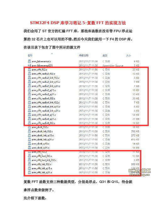
STM32F4 DSP库学习笔记5-复数FFT的实现方法我们会用了ST官方的汇编FFT库,那些库函数在没有带FPU浮点运算的32芯片上也可以用的不错。
然后今天我们就用一下F4的DSP库。
在该目录下包含了图中所示的源文件复数FFT函数支持三种数据类型,分别是浮点,Q31和Q15,待会就拿浮点数来做例子。
先介绍下函数:void arm_cfft_f32(const arm_cfft_instance_f32 * S,float32_t * p1,uint8_t ifftFlag,uint8_t bitReverseFlag);arm_cfft_instance_f32 * S是一个结构体指针这个结构体包含FFT运算的旋转因子和位反转表,就相当于一个常量,我们不用去管它。
float32_t * p1,是输入复数数组的地址,长度应该是运算点数的两倍,注意的是输入和输出共用一块缓存uint8_t ifftFlag,是运算的正反标志ifftFlag=1是反变换。
ifftFlag=0是正变换uint8_t bitReverseFlag,是flag that enables (bitReverseFlag=1) or disables (bitReverseFlag =0) bit好,然后就只要这一句话就可以计算复数的FFT正变换arm_cfft_f32(&arm_cfft_sR_f32_len1024,testInput,0, 1);计算出结果后,用下面语句就可以求出幅值了;arm_cmplx_mag_f32(testInput, testOutput, 1024);关于arm_cmplx_mag_f32(testInput, testOutput, 1024),它的原型是:void arm_cmplx_mag_f32(float32_t * pSrc,float32_t * pDst,uint32_t numSamples);这个函数是求复数的模值float32_t * pSrc,是输入数组地址float32_t * pDst,是输出数组地址uint32_t numSamples是运算点数当然上面语句中testInput数组的长度是testOutput数组的两倍。
BiLSTM-CRF学习笔记(原理和理解)维特比

BiLSTM-CRF学习笔记(原理和理解)维特⽐BiLSTM-CRF 被提出⽤于NER或者词性标注,效果⽐单纯的CRF或者lstm或者bilstm效果都要好。
根据pytorch官⽅指南(),实现了BiLSTM-CRF⼀个toy级别的源码。
下⾯是我个⼈的学习理解过程。
1. LSTMLSTM的原理前⼈已经解释的⾮常清楚了:BiLSTM-CRF中,BiLSTM部分主要⽤于,根据⼀个单词的上下⽂,给出当前单词对应标签的概率分布,可以把BiLSTM看成⼀个编码层。
⽐如,对于标签集{N, V, O}和单词China,BiLSTM可能输出形如(0.88,-1.23,0.03)的⾮归⼀化概率分布。
这个分布我们看作是crf的特征分布输⼊,那么在CRF中我们需要学习的就是特征转移概率。
2. CRF主要讲⼀下代码中要⽤到的CRF的预测(维特⽐解码)维特⽐算法流程:1.求出位置1的各个标记的⾮规范化概率δ1(j)δ1(j)δ1(j)=w∗F1(y0=START,yi=j,x),j=1,2,…,mδ1(j)=w∗F1(y0=START,yi=j,x),j=1,2,…,m2.由递推公式(前后向概率计算)δi(l)=max(1≤j≤m){δi−1(j)+w∗Fi(yi−1=j,yi=l,x)},l=1,2,…,lδi(l)=max(1≤j≤m){δi−1(j)+w∗Fi(yi−1=j,yi=l,x)},l=1,2,…,l每⼀步都保留当前所有可能的状态ll 对应的最⼤的⾮规范化概率,并将最⼤⾮规范化概率状态对应的路径(当前状态得到最⼤概率时上⼀步的状态yiyi)记录Ψi(l)=argmax(1≤j≤m){δi−1(j)+w∗Fi(yi−1=j,yi=l,x)}=argmaxδi(l),l=1,2,…,mΨi(l)=arg m ax(1≤j≤m){δi−1(j)+w∗Fi(yi−1=j,yi=l,x)}=argmaxδi(l),l=1,2,…,m就是PijPij的取值有m*m个,对每⼀个yjyj,都确定⼀个(⽽不是可能的m个)能最⼤化概率的yiyi状态3.递推到i=ni=n时终⽌这时候求得⾮规范化概率的最⼤值为maxy{w∗F(y,x)}=max(1≤j≤m)δn(j)=max(1≤j≤m){δn−1(j)+w∗Fn(yn−1=Ψn−1(k),yi=l,x)},l=1,2,…,mmaxy{w∗F(y,x)}=max(1≤j≤m)δn(j)=max(1≤j≤m) {δn−1(j)+w∗Fn(yn−1=Ψn−1(k),yi=l,x)},l=1,2,…,m最优路径终点y∗n=argmax(1≤j≤m)δn(j)yn∗=arg m ax(1≤j≤m)δn(j)4.递归路径由最优路径终点递归得到的最优路径(由当前最⼤概率状态状态对应的上⼀步状态,然后递归)y∗i=Ψi+1(y∗i+1),i=n−1,n−2,…,1yi∗=Ψi+1(yi+1∗),i=n−1,n−2,…,1求得最优路径:y∗=(y∗1,y∗2,…,y∗n)Ty∗=(y1∗,y2∗,…,yn∗)T3. 损失函数最后由CRF输出,损失函数的形式主要由CRF给出在BiLSTM-CRF中,给定输⼊序列X,⽹络输出对应的标注序列y,得分为S(X,y)=∑ni=0Ayi,yi+1+∑ni=1Pi,yiS(X,y)=∑i=0nAyi,yi+1+∑i=1nPi,yi(转移概率和状态概率之和)利⽤softmax函数,我们为每⼀个正确的tag序列y定义⼀个概率值p(y│X)=eS(X,y)∑y'∈YXeS(X,y')p(y│X)=eS(X,y)∑y′∈YXeS(X,y′)在训练中,我们的⽬标就是最⼤化概率p(y│X) ,怎么最⼤化呢,⽤对数似然(因为p(y│X)中存在指数和除法,对数似然可以化简这些运算)对数似然形式如下:log(p(y│X)=loges(X,y)∑y∈YXes(X,y′)=S(X,y)−log(∑y′∈YXes(X,y′))log(p(y│X)=log e s(X,y)∑y∈YXes(X,y′)=S(X,y)−log(∑y′∈YXes(X,y′))最⼤化这个对数似然,就是最⼩化他的相反数:¥−log(p(y│X))=log(∑y′∈YXes(X,y′))−S(X,y)−log(p(y│X))=log(∑y′∈YXes(X,y′))−S(X,y)$(loss function/object function)最⼩化可以借助梯度下降实现在对损失函数进⾏计算的时候,前⼀项S(X,y)S(X,y)很容易计算,后⼀项log(∑y′∈YXes(X,y′))log(∑y′∈YXes(X,y′))⽐较复杂,计算过程中由于指数较⼤常常会出现上溢或者下溢,由公式 log∑e(xi)=a+log∑e(xi−a)log∑e(xi)=a+log∑e(xi−a),可以借助a对指数进⾏放缩,通常a取xixi的最⼤值(即a=max[Xi]a=max[Xi]),这可以保证指数最⼤不会超过0,于是你就不会上溢出。
STM32F103学习笔记(五) 外部中断

STM32F103学习笔记(五)外部中断首先是外部中断基本的概念:STM32 的每个IO 都可以作为外部中断的中断输入口,这点也是STM32 的强大之处。
STM32F103 的中断控制器支持19 个外部中断/事件请求。
每个中断设有状态位,每个中断/事件都有独立的触发和屏蔽设置。
STM32F103 的19 个外部中断为:线0~15:对应外部IO 口的输入中断。
线16:连接到PVD 输出。
线17:连接到RTC 闹钟事件。
线18:连接到USB 唤醒事件。
线16~18还没有学到只看了线0~15。
每个中断线对应着7个GPIO口,形成映射关系,以线0 为例:它对应了GPIOA.0、GPIOB.0、GPIOC.0、GPIOD.0、GPIOE.0、GPIOF.0、GPIOG.0。
而中断线每次只能连接到1 个IO 口上,这样就需要通过配置来决定对应的中断线配置到哪个GPIO 上了。
下面我们看看GPIO 跟中断线的映射关系图:根据映射关系,就开始配置按键对应GPIO口和中断的映射了:[csharp] view plain copy <pre name="code" class="csharp"><prename="code" class="html">void EXTIX_Init(void){ EXTI_InitTypeDef EXTI_InitStructure;NVIC_InitTypeDef NVIC_InitStructure; KEY_Init(); // 按键端口初始化RCC_APB2PeriphClockCmd(RCC_APB2Periph_AFIO,EN ABLE); //使能复用功能时钟//GPIOE.2 中断线以及中断初始化配置下降沿触发GPIO_EXTILineConfig(GPIO_PortSourceGPIOE,GPIO_Pi nSource2);EXTI_InitStructure.EXTI_Line=EXTI_Line2; //KEY2 EXTI_InitStructure.EXTI_Mode = EXTI_Mode_Interrupt; EXTI_InitStructure.EXTI_Trigger = EXTI_Trigger_Falling;EXTI_InitStructure.EXTI_LineCmd = ENABLE;EXTI_Init(&EXTI_InitStructure); //根据EXTI_InitStruct中指定的参数初始化外设EXTI寄存器//GPIOE.3 中断线以及中断初始化配置下降沿触发//KEY1GPIO_EXTILineConfig(GPIO_PortSourceGPIOE,GPIO_Pi nSource3);EXTI_InitStructure.EXTI_Line=EXTI_Line3;EXTI_Init(&EXTI_InitStructure); //根据EXTI_InitStruct中指定的参数初始化外设EXTI寄存器//GPIOE.4 中断线以及中断初始化配置下降沿触发//KEY0GPIO_EXTILineConfig(GPIO_PortSourceGPIOE,GPIO_Pi nSource4);EXTI_InitStructure.EXTI_Line=EXTI_Line4;EXTI_Init(&EXTI_InitStructure); //根据EXTI_InitStruct中指定的参数初始化外设EXTI寄存器//GPIOA.0 中断线以及中断初始化配置上升沿触发PA0 WK_UPGPIO_EXTILineConfig(GPIO_PortSourceGPIOA,GPIO_Pi nSource0);EXTI_InitStructure.EXTI_Line=EXTI_Line0;EXTI_InitStructure.EXTI_Trigger = EXTI_Trigger_Rising; EXTI_Init(&EXTI_InitStructure); //根据EXTI_InitStruct中指定的参数初始化外设EXTI寄存器NVIC_InitStructure.NVIC_IRQChannel = EXTI0_IRQn;//使能按键WK_UP所在的外部中断通道NVIC_InitStructure.NVIC_IRQChannelPreemptionPriority = 0x02; //抢占优先级2,NVIC_InitStructure.NVIC_IRQChannelSubPriority = 0x03; //子优先级3NVIC_InitStructure.NVIC_IRQChannelCmd = ENABLE; //使能外部中断通道NVIC_Init(&NVIC_InitStructure);NVIC_InitStructure.NVIC_IRQChannel = EXTI2_IRQn;//使能按键KEY2所在的外部中断通道NVIC_InitStructure.NVIC_IRQChannelPreemptionPriority = 0x02; //抢占优先级2,NVIC_InitStructure.NVIC_IRQChannelSubPriority = 0x02; //子优先级2NVIC_InitStructure.NVIC_IRQChannelCmd = ENABLE; //使能外部中断通道NVIC_Init(&NVIC_InitStructure);NVIC_InitStructure.NVIC_IRQChannel = EXTI3_IRQn;//使能按键KEY1所在的外部中断通道NVIC_InitStructure.NVIC_IRQChannelPreemptionPriority = 0x02; //抢占优先级2NVIC_InitStructure.NVIC_IRQChannelSubPriority = 0x01; //子优先级1NVIC_InitStructure.NVIC_IRQChannelCmd = ENABLE; //使能外部中断通道NVIC_Init(&NVIC_InitStructure); //根据NVIC_InitStruct中指定的参数初始化外设NVIC寄存器NVIC_InitStructure.NVIC_IRQChannel = EXTI4_IRQn;//使能按键KEY0所在的外部中断通道NVIC_InitStructure.NVIC_IRQChannelPreemptionPriority = 0x02; //抢占优先级2NVIC_InitStructure.NVIC_IRQChannelSubPriority = 0x00; //子优先级0NVIC_InitStructure.NVIC_IRQChannelCmd = ENABLE; //使能外部中断通道NVIC_Init(&NVIC_InitStructure); //根据NVIC_InitStruct中指定的参数初始化外设NVIC寄存器} //外部中断0服务程序voidEXTI0_IRQHandler(void) { delay_ms(10);//消抖if(KEY3==1) //WK_UP按键{ BEEP=!BEEP; } EXTI_ClearITPendingBit(EXTI_Line0); //清除LINE0上的中断标志位} //外部中断2服务程序voidEXTI2_IRQHandler(void) { delay_ms(10);//消抖if(KEY2==0) //按键KEY2{ LED0=!LED0; }EXTI_ClearITPendingBit(EXTI_Line2); //清除LINE2上的中断标志位} //外部中断3服务程序voidEXTI3_IRQHandler(void) { delay_ms(10);//消抖if(KEY1==0) //按键KEY1{ LED1=!LED1; }EXTI_ClearITPendingBit(EXTI_Line3); //清除LINE3上的中断标志位} void EXTI4_IRQHandler(void){ delay_ms(10);//消抖if(KEY0==0) //按键KEY0 { LED0=!LED0;LED1=!LED1; }EXTI_ClearITPendingBit(EXTI_Line4); //清除LINE4上的中断标志位} [html] view plain copy。
STM32f103C8T6入门学习记录

STM32自学笔记作者:忙碌的小姚新浪微博:@忙碌的小姚新浪博客:/mlxiaoyao222目录STM32 自学笔记 (1)第一章 (3)我与STM32 的那些日子 (3)第二章 (4)使用固件库建立一个工程 (4)1、了解STM32F103的固件库 (4)2、创建第一个工程 (4)3、接下来就是管理工程文件了 (9)4、编写main.c 和文件路径 (10)第三章 (14)STM32点亮第一个LED 使用keil for ARM MDK 软件仿真 (14)1、Main.c 函数代码: (14)2、代码分析: (15)3、软件仿真介绍: (16)第四章 (19)串口的使用 (19)1、为什么要用串口? (19)2、STM32跟PC机(也就是电脑)如何连接 (19)3、代码分析 (20)4、仿真及调试 (23)5、串口接收数据 (25)第五章 (27)通用定时器的使用 (27)1、STM32F103内部定时器有哪些? (27)2、如何进行程序编写 (27)3仿真结果观察 (30)4对第四章串口的补充 (31)5工程代码 (35)第一章我与STM32 的那些日子STM32这块板子是在阿莫上跟一个老师买的,砍了半天100块钱。
包括一个Jlink v8仿真器(好像65块左右),和一块STM32系统板。
那已是一年前的事了。
那时我刚大三,刚学了半年51,于是想学点更高级的。
但我好像属于三分钟热度的这种人,买回来学了一个星期,就学不动了,寄存器操作,固件库的使用根本就没明白是怎么一回事,之后就没有然后了。
现在看到那块板子,总有一种说不出的滋味,要是当时能咬牙切齿努力学习,说不定现在也不会安静地坐在电脑前一字一句敲打这篇激励性文章了。
对于STM32我没用任何基础,唯一有的也只是一年前学的那一个星期,不过那已不重要了,我现在仍是一个小白。
作为一个初学者,也许是坐井观天,看的是片面的,可能有很多观点是错误的,希望读者朋友能勇于指出来。
STM32F10xxx 正交编码器接口应用笔记
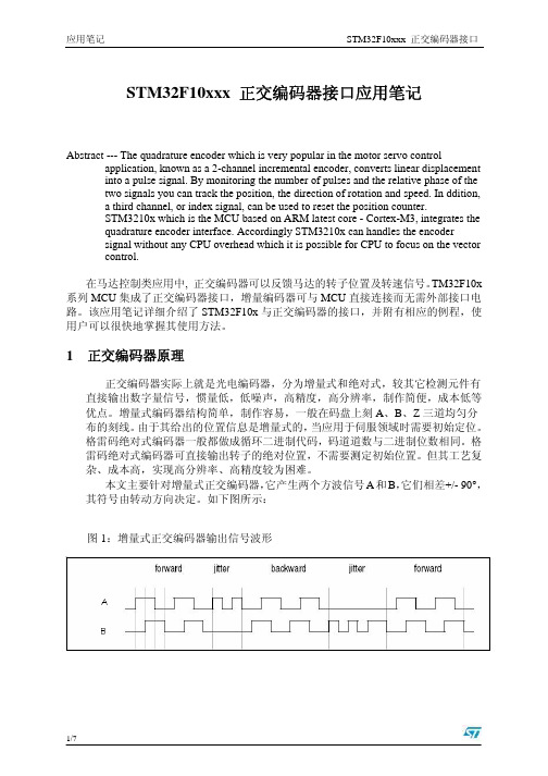
正交编码器接口应用笔记STM32F10xxxAbstract --- The quadrature encoder which is very popular in the motor servo control application, known as a 2-channel incremental encoder, converts linear displacementinto a pulse signal. By monitoring the number of pulses and the relative phase of thetwo signals you can track the position, the direction of rotation and speed. In ddition,a third channel, or index signal, can be used to reset the position counter.STM3210x which is the MCU based on ARM latest core - Cortex-M3, integrates thequadrature encoder interface. Accordingly STM3210x can handles the encodersignal without any CPU overhead which it is possible for CPU to focus on the vectorcontrol.在马达控制类应用中, 正交编码器可以反馈马达的转子位置及转速信号。
TM32F10x 系列MCU集成了正交编码器接口,增量编码器可与MCU直接连接而无需外部接口电路。
该应用笔记详细介绍了STM32F10x与正交编码器的接口,并附有相应的例程,使用户可以很快地掌握其使用方法。
stm32f3 标准库函数说明
一、STM32F3标准库简介STM32F3是STM32系列微控制器的一款产品,它采用Cortex-M4内核,具有丰富的外设和功能。
STM32F3标准库是由STMicroelectronics官方提供的一套用于开发STM32F3系列微控制器的函数库,它包含了丰富的函数和例程,能够为开发者提供方便快捷的开发支持。
二、STM32F3标准库函数分类1. GPIO函数GPIO函数是用于对STM32F3微控制器的GPIO端口进行操作的函数集合,包括对GPIO端口的初始化、输入输出设置、读取状态等功能。
2. 定时器函数定时器函数是用于对STM32F3微控制器的定时器进行操作的函数集合,包括定时器的初始化、启动、停止、中断处理等功能。
3. 中断函数中断函数是用于对STM32F3微控制器的中断进行操作的函数集合,包括中断的使能、优先级设置、中断向量表的编写等功能。
4. 串口函数串口函数是用于对STM32F3微控制器的串口进行操作的函数集合,包括串口的初始化、发送数据、接收数据、中断处理等功能。
5. ADC/DAC函数ADC/DAC函数是用于对STM32F3微控制器的模数转换器和数模转换器进行操作的函数集合,包括ADC/DAC的初始化、转换启动、中断处理、数据处理等功能。
6. 外设驱动函数外设驱动函数是用于对STM32F3微控制器的外设进行操作的函数集合,包括I2C、SPI、USB、CAN等外设的初始化、数据传输、中断处理等功能。
三、STM32F3标准库函数使用示例以下是一些STM32F3标准库函数的使用示例,供开发者参考:1. GPIO函数示例:```c#include "stm32f3xx.h"int main(){GPIO_InitTypeDef GPIO_InitStructure;RCC_AHBPeriphClockCmd(RCC_AHBPeriph_GPIOA, ENABLE); GPIO_InitStructure.GPIO_Pin = GPIO_Pin_0;GPIO_InitStructure.GPIO_Mode = GPIO_Mode_OUT;GPIO_InitStructure.GPIO_Speed = GPIO_Speed_2MHz;GPIO_InitStructure.GPIO_OType = GPIO_OType_PP;GPIO_InitStructure.GPIO_PuPd = GPIO_PuPd_NOPULL;GPIO_Init(GPIOA, GPIO_InitStructure);while(1){GPIO_SetBits(GPIOA, GPIO_Pin_0);//延时一段时间GPIO_ResetBits(GPIOA, GPIO_Pin_0);//延时一段时间}}```2. 定时器函数示例:```c#include "stm32f3xx.h"int main(){TIM_TimeBaseInitTypeDef TIM_TimeBaseStructure;RCC_APB1PeriphClockCmd(RCC_APB1Periph_TIM2, ENABLE); TIM_TimeBaseStructure.TIM_Prescaler= 7200 - 1;TIM_TimeBaseStructure.TIM_Period= 10000 - 1;TIM_TimeBaseStructure.TIM_CounterMode=TIM_CounterMode_Up;TIM_TimeBaseInit(TIM2, TIM_TimeBaseStructure);TIM_Cmd(TIM2, ENABLE);while(1){if(TIM_GetFlagStatus(TIM2, TIM_FLAG_Update)!= RESET) {//定时器计数器达到设定值时执行的操作TIM_ClearFlag(TIM2, TIM_FLAG_Update);}}```四、总结STM32F3标准库函数是用于开发STM32F3微控制器的重要工具,通过学习和掌握标准库函数的使用方法,开发者可以更加高效地进行STM32F3系列微控制器的开发工作。
STM32F4学习笔记之USART(使用固件库,查询方式)

USART_SendData(USART1, USART_ReceiveData(USART1));
while (USART_GetFlagStatus(USART1, USART_FLAG_TC) == RESET);
}
}
}
GPIO_StructInit(&GPIO_InitStructure);
GPIO_InitStructure.GPIO_OType = GPIO_OType_PP;
GPIO_InitStructure.GPIO_Mode = GPIO_Mode_AF;
GPIO_InitStructure.GPIO_Pin = GPIO_Pin_9 | GPIO_Pin_10;
GPIO_InitStructure.GPIO_Speed = GPIO_Speed_50MHz;
GPIO_Init(GPIOA, &GPIO_InitStructure);
USART_ART_BaudRate = 115200;
USART_ART_WordLength = USART_WordLength_8b;
USART_ART_Mode = USART_Mode_Rx | USART_Mode_Tx; //工作模式
USART_Init(USARTx, &USART_InitStructure); //写入配置信息
USART_Cmd(USARTx, ENABLE); //使能串口模块
xxx=USART_ReceiveData(USARTx) //读取接收到的数据
程序举例:
int main(void)
{
GPIO_InitTypeDef GPIO_InitStructure;
stm32的傅里叶变换库

stm32的傅里叶变换库
STMicroelectronics 提供了一个封装了傅里叶变换功能的库,
称为 STM32 DSP 库。
该库是基于 ST DSP 库的延伸,为用户
提供了一组函数,用于在 STM32 微控制器上执行各种数字信
号处理任务,包括傅里叶变换。
该库提供了几个函数来执行不同类型的傅里叶变换,例如基于浮点数的快速傅里叶变换(FFT)、基于浮点数的傅里叶变换(DFT)等。
用户可以根据具体的应用需求选择适当的函数来实现所需的傅里叶变换操作。
在 STM32 DSP 库中,相关的函数包括:
1. arm_rfft_f32():用于计算实数输入的快速傅里叶变换(RFFT)。
该函数将实数输入序列转换为一半长度的复数输
出序列。
2. arm_cfft_f32():用于计算复数输入的快速傅里叶变换(CFFT)。
该函数将复数输入序列转换为相同长度的复数输
出序列。
3. arm_dct4_f32():用于计算离散余弦变换(DCT)的 Type-IV。
该函数将实数输入序列转换为相同长度的实数输出序列。
4. arm_cfft_radix4_f32():用于计算基于浮点数的快速傅里叶变换(FFT)。
该函数将复数输入序列转换为相同长度的复数输
出序列。
除了这些函数,STM32 DSP 库还提供了其他一些函数,用于实现更高级的傅里叶变换操作,例如带通滤波、噪声降低等。
使用 STM32 DSP 库进行傅里叶变换的详细说明可在ST官方网站上的相关文档中找到。
RT-Thread4.0+STM32F407学习笔记1
RT-Thread4.0+STM32F407学习笔记1RT Thread 4.0提供了新的BSP框架新 BSP 框架的主要特性如下:提供多系列 BSP 模板,⼤⼤降低新 BSP 的添加难度;每个 BSP 都配有齐全的驱动⽂件,开发者可以⽅便地使⽤所有驱动;开发者可以使⽤ CubeMX ⼯具对 BSP 进⾏图形化配置;由于Hal库是以后主流,在使⽤STD库对STM32很熟悉后,建议转到Hal库本⽂参考官⽅《STM32系列BSP制作教程》,由于官⽅提供的CubeMX与Hal库版本固定,不⼀定适⽤所有初步使⽤的⼈,本⽂使⽤⾃⼰的CubeMX制作BSP并强调注意事项。
其中⼀些解释如内容说明、Scons、Env等,详细参见《STM32系列BSP制作教程》1. BSP 制作⽅法BSP 的制作过程分为如下五个步骤:1. 复制通⽤模板2. 使⽤ CubeMX ⼯具配置⼯程3. 修改 BSP 中的 Kconfig ⽂件4. 修改构建⼯程相关⽂件5. 重新⽣成⼯程1.1 复制通⽤模板复制 rt-thread-4.0.0\bsp\stm32\libraries\templates\stm32f4xx重命名为 rt-thread-4.0.0\bsp\stm32\stm32f407-pz6808l1.2 使⽤CubeMX配置⼯程本⽂使⽤的是CubeMX 5.2版本配置RCC使能外部晶振使能调试使能UART时钟配置⼯程管理,⽣成到BSP框架⾥的⽂件夹下⽣成⼯程如下1.3 HAL库替换删除MDK-ARM⽂件夹复制Drivers到 rt-thread-4.0.0\bsp\stm32\libraries ⽂件下并重命名为 STM32F4xx_HAL_502从模板中复制SConscript⽂件1.4⽂件修改rt-thread-4.0.0\bsp\stm32\stm32f407-pz6808l\board\board.c⽤⽣成的main.c中的 SystemClock_Config 进⾏替换修改board/Kconfig⽂件修改链接脚本填写对应芯⽚的Flah和RAM⼤⼩,主要有些芯⽚有⾮连续RAM,填写RAM1⼤⼩即可修改主⼯程⽬录下的修改 SConstruct 链接⾃⼰的HAL库修改 board ⽬录下的 SConscript修改为需要制作BSP的芯⽚型号对应内容注意 stm32f4xx_hal_msp.c ⽂件查看是否包含有串⼝初始化 HAL_UART_MspInit ,没有则⽤MX重新⽣成,否则程序运⾏会出错(串⼝异常)1.5 使⽤Env⼯具⽣成⼯程打开模板 template.uvprojx ,对⼯程进⾏相关设置,这样以后每次⽂件的改动需要重新⽣成⼯程时,⼯程就不⽤再设置了;在 env 界⾯输⼊命令 menuconfig 对⼯程进⾏配置,并⽣成新的 rtconfig.h ⽂件。
STM32F401(411)应用笔记
ᇐᰬಞ
TIMX_BKIN
儎㓝ᇐᰬಞ TIM1
TIMx_TRGO/ITRx
䙐⭞ᇐᰬಞ
TIM5 TIM4 TIM3
TIM2
TIMx_TRGO/ITRx
TIM11_CH1 TIM11
TIMx_TRGO/
SOF/ITRx
ITRx
TIM10
TIM9
䙐⭞ᇐᰬಞ
ӻ൞STM32F411xр
㌱㔕
EXTI VBAT VREFIN
2.5.2 从通信接口到 DMA . . . . . . . . . . . . . . . . . . . . . . . . . . . . . . . . . . . . . . . . 12
2.6 DMA 模块 . . . . . . . . . . . . . . . . . . . . . . . . . . . . . . . . . . . . . . . . . . . . . . . . . 12
AN4646 应用笔记
STM32F401 和 STM32F411 系列上的外设内部互联
前言
在 STM32F4 系列最高性能和最低价格的基础上,STM32F401/411 外设可以通过名为 “ 外设 内部互联矩阵 ” 的网络实现自主通信,无需 CPU 介入。
STM32F401/411 系列产品的这一新特性增强了 CPU 的实时性能,并显著降低了功耗。
本文档首先描述了外设内部互联矩阵的特性,然后概述了外设内部互联以及如何根据应用对 其进行配置。详细的应用实例使描述更加完整。
本应用笔记必须与 STM32F401 系列参考手册 (RM0383) 和 STM32F411 系列参考手册 (RM0368) 一起阅读。两参考手册均可从 /stm32 下载。
lan8720

#define PHY_FULLDUPLEX_100M
((uint16_t)0x2100)
#define PHY_HALFDUPLEX_100M
((uint16_t)0x2000)
#define PHY_FULLDUPLEX_10M
((uint16_t)0x0100)
#define PHY_HALFDUPLEX_10M
定义了两个全局指针变量 分别指向下一个要发送或接收的数据包
__IO ETH_DMADESCTypeDef *DMATxDescToSet; __IO ETH_DMADESCTypeDef *DMARxDescToGet;
DMA描述符位定义
//DMA描述符框架 用于DMA描述符接收到的数据交给LWIP typedef struct{
u32 length;
u32 buffer; __IO ETH_DMADESCTypeDef *descriptor; }FrameTypeDef;
Descriptor0 -> Descriptor1 -> Descriptor2 -> Descriptor3 DMA描述符链式结构
((uint16_t)0x0000)
#define PHY_AutoNegotiation
((uint16_t)0x1000)
#define PHY_Restart_AutoNegotiation ((uint16_t)0x0200)
#define PHY_Powerdown
((uint16_t)0x0800)
#ifdef USE_ENHANCED_DMA_DESCRIPTORS uint32_t ExtendedStatus; uint32_t Reserved1; uint32_t TimeStampLow; uint32_t TimeStampHigh;
STM32库函数汇总
STM32库函数汇总STMicroelectronics提供了一套完整的软件开发工具包(STMCube),其中包含了一系列的库函数,用于简化STM32的开发过程。
下面是一些常用的STM32库函数的简要介绍:1.GPIO库函数:用于设置和控制GPIO(通用输入输出)引脚状态,包括初始化、读取和写入引脚状态等。
2.外部中断库函数:用于配置和控制外部中断功能,包括触发方式、中断优先级等。
3.定时器库函数:用于配置和控制定时器功能,包括计数模式、定时器中断、PWM输出等。
4.ADC库函数:用于配置和控制ADC(模数转换器)功能,包括参考电压、采样周期、数据读取等。
5.UART库函数:用于配置和控制UART(串行通用异步收发器)功能,包括波特率、数据传输、中断接收等。
6.SPI库函数:用于配置和控制SPI(串行外设接口)功能,包括传输方式、模式、速率、中断接收等。
7.I2C库函数:用于配置和控制I2C(串行外设接口)功能,包括传输方式、速率、地址、中断接收等。
8.DMA库函数:用于配置和控制DMA(直接内存访问)功能,实现高速数据传输,减轻CPU负担。
9.NVIC库函数:用于配置和控制NVIC(嵌套向量中断控制器)功能,包括中断优先级、使能、清除等。
10.RCC库函数:用于配置和控制RCC(时钟控制)功能,包括系统时钟频率、外设时钟使能、时钟源选择等。
11. FLASH库函数:用于配置和控制Flash存储器功能,包括写入、擦除、读取等。
12.PWM库函数:用于配置和控制PWM(脉冲宽度调制)功能,用于控制电机速度、LED亮度等。
B库函数:用于配置和控制USB(通用串行总线)功能,实现USB设备或主机功能。
14.CRC库函数:用于配置和控制CRC(循环冗余校验)功能,用于数据校验。
15.RTC库函数:用于配置和控制RTC(实时时钟)功能,包括时钟设置、中断控制等。
以上是一些常用的STM32库函数,通过使用这些库函数,开发者可以快速高效地开发STM32相关的应用。
STM32F4官方评估板 笔记
STM32F407VGT6 ST官方评估板无责任笔记①②③④⑤⑥⑦⑧⑨⑩Writen By 钟礼浩华南农业大学工程学院QQ371724290一.系统初始化①void SystemInit(void);子函数:static void SetSysClock(void)关键值:/* PLL_VCO = (HSE_V ALUE or HSI_V ALUE / PLL_M) * PLL_N */#define PLL_M 8 //直接修改为晶振值即得到168MHz系统时钟#define PLL_N 336/* SYSCLK = PLL_VCO / PLL_P */#define PLL_P 2/* USB OTG FS, SDIO and RNG Clock = PLL_VCO / PLLQ */#define PLL_Q 7* Supported STM32F4xx device revision | Rev A* System Clock source | PLL (HSE)* SYSCLK(Hz) | 168000000* HCLK(Hz) | 168000000* AHB Prescaler | 1* APB1 Prescaler | 4* APB2 Prescaler | 2* HSE Frequency(Hz) | 25000000* PLL_M | 25* PLL_N | 336* PLL_P | 2* PLL_Q | 7* PLLI2S_N | NA* PLLI2S_R | NA* I2S input clock | NA* VDD(V) | 3.3* Main regulator output voltage | Scale1 mode* Flash Latency(WS) | 5* Prefetch Buffer | OFF* Instruction cache | ON* Data cache | ON* Require 48MHz for USB OTG FS, | Enabled* SDIO and RNG clock |二.通用io结构体设置①typedef struct{uint32_t GPIO_Pin; //针脚This parameter can be any value of @ref GPIO_pins_define */ GPIOMode_TypeDef GPIO_Mode; //模式This parameter can be a value of @ref GPIOMode_TypeDef */ GPIOSpeed_TypeDef GPIO_Speed; //速度This parameter can be a value of @ref GPIOSpeed_TypeDef */ GPIOOType_TypeDef GPIO_OType; //输出物理模式推挽or 开漏This parameter can be a value of @ref GPIOOType_TypeDef */ GPIOPuPd_TypeDef GPIO_PuPd; //上下拉电阻设置This parameter can be a value of @ref GPIOPuPd_TypeDef */ }GPIO_InitTypeDef;Pin选择:#define GPIO_Pin_0 ((uint16_t)0x0001) /* Pin 0 selected */#define GPIO_Pin_1 ((uint16_t)0x0002) /* Pin 1 selected */#define GPIO_Pin_2 ((uint16_t)0x0004) /* Pin 2 selected */#define GPIO_Pin_3 ((uint16_t)0x0008) /* Pin 3 selected */#define GPIO_Pin_4 ((uint16_t)0x0010) /* Pin 4 selected */#define GPIO_Pin_5 ((uint16_t)0x0020) /* Pin 5 selected */#define GPIO_Pin_6 ((uint16_t)0x0040) /* Pin 6 selected */#define GPIO_Pin_7 ((uint16_t)0x0080) /* Pin 7 selected */#define GPIO_Pin_8 ((uint16_t)0x0100) /* Pin 8 selected */#define GPIO_Pin_9 ((uint16_t)0x0200) /* Pin 9 selected */#define GPIO_Pin_10 ((uint16_t)0x0400) /* Pin 10 selected */#define GPIO_Pin_11 ((uint16_t)0x0800) /* Pin 11 selected */#define GPIO_Pin_12 ((uint16_t)0x1000) /* Pin 12 selected */#define GPIO_Pin_13 ((uint16_t)0x2000) /* Pin 13 selected */#define GPIO_Pin_14 ((uint16_t)0x4000) /* Pin 14 selected */#define GPIO_Pin_15 ((uint16_t)0x8000) /* Pin 15 selected */#define GPIO_Pin_All ((uint16_t)0xFFFF) /* All pins selected */Mode选择:typedef enum{GPIO_Mode_IN = 0x00, /*!< GPIO Input Mode */GPIO_Mode_OUT = 0x01, /*!< GPIO Output Mode */GPIO_Mode_AF = 0x02, /*!< GPIO Alternate function Mode */GPIO_Mode_AN = 0x03 /*!< GPIO Analog Mode */}GPIOMode_TypeDef;Speed速度设置:typedef enum{GPIO_Speed_2MHz = 0x00, /*!< Low speed */GPIO_Speed_25MHz = 0x01, /*!< Medium speed */GPIO_Speed_50MHz = 0x02, /*!< Fast speed */GPIO_Speed_100MHz = 0x03 /*!< High speed on 30 pF (80 MHz Output max speed on 15 pF) */ }GPIOSpeed_TypeDef;OT ype输出物理性质设置:typedef enum{GPIO_OType_PP = 0x00,GPIO_OType_OD = 0x01}GPIOOType_TypeDef;PuPd上下拉电阻设置:typedef enum{GPIO_PuPd_NOPULL = 0x00,GPIO_PuPd_UP = 0x01,GPIO_PuPd_DOWN = 0x02}GPIOPuPd_TypeDef;②开相关寄存器时钟:(注意开syscfg在APB2)void RCC_AHB1PeriphClockCmd(uint32_t RCC_AHB1Periph, FunctionalState NewState)void RCC_AHB2PeriphClockCmd(uint32_t RCC_AHB2Periph, FunctionalState NewState)void RCC_AHB3PeriphClockCmd(uint32_t RCC_AHB3Periph, FunctionalState NewState)void RCC_APB1PeriphClockCmd(uint32_t RCC_APB1Periph, FunctionalState NewState)void RCC_APB2PeriphClockCmd(uint32_t RCC_APB2Periph, FunctionalState NewState)AHB1首位形参:RCC_AHB1Periph_GPIOA: GPIOA clockRCC_AHB1Periph_GPIOB: GPIOB clockRCC_AHB1Periph_GPIOC: GPIOC clockRCC_AHB1Periph_GPIOD: GPIOD clockRCC_AHB1Periph_GPIOE: GPIOE clockRCC_AHB1Periph_GPIOF: GPIOF clockRCC_AHB1Periph_GPIOG: GPIOG clockRCC_AHB1Periph_GPIOG: GPIOG clockRCC_AHB1Periph_GPIOI: GPIOI clockRCC_AHB1Periph_CRC: CRC clockRCC_AHB1Periph_BKPSRAM: BKPSRAM interface clock RCC_AHB1Periph_CCMDA TARAMEN: CCM data RAM interface clock RCC_AHB1Periph_DMA1: DMA1 clockRCC_AHB1Periph_DMA2: DMA2 clockRCC_AHB1Periph_ETH_MAC: Ethernet MAC clockRCC_AHB1Periph_ETH_MAC_Tx: Ethernet Transmission clock RCC_AHB1Periph_ETH_MAC_Rx: Ethernet Reception clockRCC_AHB1Periph_ETH_MAC_PTP: Ethernet PTP clockRCC_AHB1Periph_OTG_HS: USB OTG HS clockRCC_AHB1Periph_OTG_HS_ULPI: USB OTG HS ULPI clockAHB2首位形参:RCC_AHB2Periph_DCMI: DCMI clockRCC_AHB2Periph_CRYP: CRYP clockRCC_AHB2Periph_HASH: HASH clockRCC_AHB2Periph_RNG: RNG clockRCC_AHB2Periph_OTG_FS: USB OTG FS clockAHB3首位形参:RCC_AHBPeriph: specifies the AHB3 peripheral to gates its clock.This parameter must be: RCC_AHB3Periph_FSMCAPB1首位形参:RCC_APB1Periph_TIM2: TIM2 clockRCC_APB1Periph_TIM3: TIM3 clockRCC_APB1Periph_TIM4: TIM4 clockRCC_APB1Periph_TIM5: TIM5 clockRCC_APB1Periph_TIM6: TIM6 clockRCC_APB1Periph_TIM7: TIM7 clockRCC_APB1Periph_TIM12: TIM12 clock RCC_APB1Periph_TIM13: TIM13 clockRCC_APB1Periph_TIM14: TIM14 clockRCC_APB1Periph_WWDG: WWDG clock RCC_APB1Periph_SPI2: SPI2 clockRCC_APB1Periph_SPI3: SPI3 clockRCC_APB1Periph_USART2: USART2 clock RCC_APB1Periph_USART3: USART3 clock RCC_APB1Periph_UART4: UART4 clock RCC_APB1Periph_UART5: UART5 clock RCC_APB1Periph_I2C1: I2C1 clockRCC_APB1Periph_I2C2: I2C2 clockRCC_APB1Periph_I2C3: I2C3 clockRCC_APB1Periph_CAN1: CAN1 clockRCC_APB1Periph_CAN2: CAN2 clockRCC_APB1Periph_PWR: PWR clockRCC_APB1Periph_DAC: DAC clockAPB2首位形参:RCC_APB2Periph_TIM1: TIM1 clockRCC_APB2Periph_TIM8: TIM8 clockRCC_APB2Periph_USART1: USART1 clock RCC_APB2Periph_USART6: USART6 clock RCC_APB2Periph_ADC1: ADC1 clockRCC_APB2Periph_ADC2: ADC2 clock RCC_APB2Periph_ADC3: ADC3 clock RCC_APB2Periph_SDIO: SDIO clockRCC_APB2Periph_SPI1: SPI1 clockRCC_APB2Periph_SYSCFG: SYSCFG clock RCC_APB2Periph_TIM9: TIM9 clockRCC_APB2Periph_TIM10: TIM10 clockRCC_APB2Periph_TIM11: TIM11 clock③GPIO_Init(GPIOx ,&GPIO_InitStructure); //与①共同协作,port与结构体为形参三.开外部中断①GPIO_InitTypeDef;EXTI_InitTypeDef;NVIC_InitTypeDef; //定义结构体②开时钟(前述)位时钟,syscfg③void GPIO_Init(GPIO_T ypeDef* GPIOx, GPIO_InitT ypeDef* GPIO_InitStruct) //GPIO设置④void SYSCFG_EXTILineConfig(uint8_t EXTI_PortSourceGPIOx, uint8_t EXTI_PinSourcex) //中断注册(port 和位)⑤typedef struct{uint32_t EXTI_Line; /*!< Specifies the EXTI lines to be enabled or disabled.This parameter can be any combination value of @ref EXTI_Lines */ EXTIMode_TypeDef EXTI_Mode; /*!< Specifies the mode for the EXTI lines.This parameter can be a value of @ref EXTIMode_TypeDef */ EXTITrigger_TypeDef EXTI_Trigger; /*!< Specifies the trigger signal active edge for the EXTI lines.This parameter can be a value of @ref EXTITrigger_TypeDef */ FunctionalState EXTI_LineCmd; /*!< Specifies the new state of the selected EXTI lines.This parameter can be set either to ENABLE or DISABLE */}EXTI_InitTypeDef;EXTI_Line:#define EXTI_Line0#define EXTI_Line1#define EXTI_Line2#define EXTI_Line3#define EXTI_Line4#define EXTI_Line5#define EXTI_Line6#define EXTI_Line7#define EXTI_Line8#define EXTI_Line9#define EXTI_Line10#define EXTI_Line11#define EXTI_Line12#define EXTI_Line13#define EXTI_Line14#define EXTI_Line15#define EXTI_Line16 PVD Output#define EXTI_Line17 RTC Alarm event#define EXTI_Line18 USB OTG FS Wakeup from suspend event#define EXTI_Line19 Ethernet Wakeup event#define EXTI_Line20 USB OTG HS (configured in FS) Wakeup event#define EXTI_Line21 RTC Tamper and Time Stamp events#define EXTI_Line22 RTC Wakeup eventEXTI_Mode:typedef enum{EXTI_Mode_Interrupt = 0x00,√EXTI_Mode_Event = 0x04}EXTIMode_TypeDef;EXTI_Trigger:typedef enum{EXTI_Trigger_Rising = 0x08,√EXTI_Trigger_Falling = 0x0C,EXTI_Trigger_Rising_Falling = 0x10}EXTITrigger_TypeDef;EXTI_LineCmd:ENABLEDISABLE⑥void EXTI_Init(EXTI_InitT ypeDef* EXTI_InitStruct) //初始化⑦typedef struct{uint8_t NVIC_IRQChannel;uint8_t NVIC_IRQChannelPreemptionPriority; // 0x00-0x0f取值uint8_t NVIC_IRQChannelSubPriority; // 0x00-0x0f取值FunctionalState NVIC_IRQChannelCmd; //ENABLE,DISABLE} NVIC_InitTypeDef;NVIC_IRQChannel:typedef enum IRQn{/****** Cortex-M4 Processor Exceptions Numbers ****************************************************************/ NonMaskableInt_IRQn = -14, /*!< 2 Non Maskable Interrupt */ MemoryManagement_IRQn = -12, /*!< 4 Cortex-M4 Memory Management Interrupt */ BusFault_IRQn = -11, /*!< 5 Cortex-M4 Bus Fault Interrupt */UsageFault_IRQn = -10, /*!< 6 Cortex-M4 Usage Fault Interrupt */ SVCall_IRQn = -5, /*!< 11 Cortex-M4 SV Call Interrupt */ DebugMonitor_IRQn = -4, /*!< 12 Cortex-M4 Debug Monitor Interrupt */ PendSV_IRQn = -2, /*!< 14 Cortex-M4 Pend SV Interrupt */ SysTick_IRQn = -1, /*!< 15 Cortex-M4 System Tick Interrupt *//****** STM32 specific Interrupt Numbers **********************************************************************/ WWDG_IRQn = 0, /*!< Window WatchDog Interrupt */ PVD_IRQn = 1, /*!< PVD through EXTI Line detection Interrupt */ TAMP_STAMP_IRQn = 2, /*!< Tamper and TimeStamp interrupts through the EXTI line */RTC_WKUP_IRQn = 3, /*!< RTC Wakeup interrupt through the EXTI line */ FLASH_IRQn = 4, /*!< FLASH global Interrupt */ RCC_IRQn = 5, /*!< RCC global Interrupt */ EXTI0_IRQn = 6, /*!< EXTI Line0 Interrupt */ EXTI1_IRQn = 7, /*!< EXTI Line1 Interrupt */ EXTI2_IRQn = 8, /*!< EXTI Line2 Interrupt */ EXTI3_IRQn = 9, /*!< EXTI Line3 Interrupt */ EXTI4_IRQn = 10, /*!< EXTI Line4 Interrupt */ DMA1_Stream0_IRQn = 11, /*!< DMA1 Stream 0 global Interrupt */ DMA1_Stream1_IRQn = 12, /*!< DMA1 Stream 1 global Interrupt */ DMA1_Stream2_IRQn = 13, /*!< DMA1 Stream 2 global Interrupt */ DMA1_Stream3_IRQn = 14, /*!< DMA1 Stream 3 global Interrupt */ DMA1_Stream4_IRQn = 15, /*!< DMA1 Stream 4 global Interrupt */ DMA1_Stream5_IRQn = 16, /*!< DMA1 Stream 5 global Interrupt */ DMA1_Stream6_IRQn = 17, /*!< DMA1 Stream 6 global Interrupt */ ADC_IRQn = 18, /*!< ADC1, ADC2 and ADC3 global Interrupts */ CAN1_TX_IRQn = 19, /*!< CAN1 TX Interrupt */ CAN1_RX0_IRQn = 20, /*!< CAN1 RX0 Interrupt */ CAN1_RX1_IRQn = 21, /*!< CAN1 RX1 Interrupt */ CAN1_SCE_IRQn = 22, /*!< CAN1 SCE Interrupt */ EXTI9_5_IRQn = 23, /*!< External Line[9:5] Interrupts */TIM1_BRK_TIM9_IRQn = 24, /*!< TIM1 Break interrupt and TIM9 global interrupt */TIM1_UP_TIM10_IRQn = 25, /*!< TIM1 Update Interrupt and TIM10 global interrupt */TIM1_TRG_COM_TIM11_IRQn = 26, /*!< TIM1 Trigger and Commutation Interrupt and TIM11 global interrupt */TIM1_CC_IRQn = 27, /*!< TIM1 Capture Compare Interrupt */ TIM2_IRQn = 28, /*!< TIM2 global Interrupt */ TIM3_IRQn = 29, /*!< TIM3 global Interrupt */ TIM4_IRQn = 30, /*!< TIM4 global Interrupt */I2C1_EV_IRQn = 31, /*!< I2C1 Event Interrupt */I2C1_ER_IRQn = 32, /*!< I2C1 Error Interrupt */I2C2_EV_IRQn = 33, /*!< I2C2 Event Interrupt */I2C2_ER_IRQn = 34, /*!< I2C2 Error Interrupt */SPI1_IRQn = 35, /*!< SPI1 global Interrupt */SPI2_IRQn = 36, /*!< SPI2 global Interrupt */ USART1_IRQn = 37, /*!< USART1 global Interrupt */ USART2_IRQn = 38, /*!< USART2 global Interrupt */ USART3_IRQn = 39, /*!< USART3 global Interrupt */ EXTI15_10_IRQn = 40, /*!< External Line[15:10] Interrupts */RTC_Alarm_IRQn = 41, /*!< RTC Alarm (A and B) through EXTI Line Interrupt */OTG_FS_WKUP_IRQn = 42, /*!< USB OTG FS Wakeup through EXTI line interrupt */ TIM8_BRK_TIM12_IRQn = 43, /*!< TIM8 Break Interrupt and TIM12 global interrupt */TIM8_UP_TIM13_IRQn = 44, /*!< TIM8 Update Interrupt and TIM13 global interrupt */TIM8_TRG_COM_TIM14_IRQn = 45, /*!< TIM8 Trigger and Commutation Interrupt and TIM14 global interrupt */TIM8_CC_IRQn = 46, /*!< TIM8 Capture Compare Interrupt */ DMA1_Stream7_IRQn = 47, /*!< DMA1 Stream7 Interrupt */ FSMC_IRQn = 48, /*!< FSMC global Interrupt */ SDIO_IRQn = 49, /*!< SDIO global Interrupt */ TIM5_IRQn = 50, /*!< TIM5 global Interrupt */ SPI3_IRQn = 51, /*!< SPI3 global Interrupt */ UART4_IRQn = 52, /*!< UART4 global Interrupt */ UART5_IRQn = 53, /*!< UART5 global Interrupt */ TIM6_DAC_IRQn = 54, /*!< TIM6 global and DAC1&2 underrun error interrupts */TIM7_IRQn = 55, /*!< TIM7 global interrupt */ DMA2_Stream0_IRQn = 56, /*!< DMA2 Stream 0 global Interrupt */ DMA2_Stream1_IRQn = 57, /*!< DMA2 Stream 1 global Interrupt */ DMA2_Stream2_IRQn = 58, /*!< DMA2 Stream 2 global Interrupt */ DMA2_Stream3_IRQn = 59, /*!< DMA2 Stream 3 global Interrupt */ DMA2_Stream4_IRQn = 60, /*!< DMA2 Stream 4 global Interrupt */ ETH_IRQn = 61, /*!< Ethernet global Interrupt */ETH_WKUP_IRQn = 62, /*!< Ethernet Wakeup through EXTI line Interrupt */ CAN2_TX_IRQn = 63, /*!< CAN2 TX Interrupt */ CAN2_RX0_IRQn = 64, /*!< CAN2 RX0 Interrupt */ CAN2_RX1_IRQn = 65, /*!< CAN2 RX1 Interrupt */ CAN2_SCE_IRQn = 66, /*!< CAN2 SCE Interrupt */ OTG_FS_IRQn = 67, /*!< USB OTG FS global Interrupt */ DMA2_Stream5_IRQn = 68, /*!< DMA2 Stream 5 global interrupt */ DMA2_Stream6_IRQn = 69, /*!< DMA2 Stream 6 global interrupt */ DMA2_Stream7_IRQn = 70, /*!< DMA2 Stream 7 global interrupt */ USART6_IRQn = 71, /*!< USART6 global interrupt */I2C3_EV_IRQn = 72, /*!< I2C3 event interrupt */I2C3_ER_IRQn = 73, /*!< I2C3 error interrupt */ OTG_HS_EP1_OUT_IRQn = 74, /*!< USB OTG HS End Point 1 Out global interrupt */ OTG_HS_EP1_IN_IRQn = 75, /*!< USB OTG HS End Point 1 In global interrupt */ OTG_HS_WKUP_IRQn = 76, /*!< USB OTG HS Wakeup through EXTI int errupt */ OTG_HS_IRQn = 77, /*!< USB OTG HS global interrupt */ DCMI_IRQn = 78, /*!< DCMI global interrupt */ CRYP_IRQn = 79, /*!< CRYP crypto global interrupt */ HASH_RNG_IRQn = 80, /*!< Hash and Rng global interrupt */ FPU_IRQn = 81 /*!< FPU global interrupt */} IRQn_Type;⑧void NVIC_Init(NVIC_InitT ypeDef* NVIC_InitStruct)----①开启中断服务函数IRQ系列:void EXTI0_IRQHandler(void) 例②void EXTI_ClearITPendingBit(uint32_t EXTI_Line) //清除标志位----------四.位操作什锦①uint8_t GPIO_ReadInputDataBit(GPIO_T ypeDef* GPIOx, uint16_t GPIO_Pin) //直接读位输入信息返回:Bit_SET(非0),Bit_RESET(0);②typedef struct{__IO uint32_t MODER;__IO uint32_t OTYPER;__IO uint32_t OSPEEDR;__IO uint32_t PUPDR;__IO uint32_t IDR;__IO uint32_t ODR; //自异或可以翻转__IO uint16_t BSRRL; //置1输出为ODR__IO uint16_t BSRRH; //置1输出为非ODR__IO uint32_t LCKR;__IO uint32_t AFR[2];} GPIO_TypeDef;五.定时器中断①TIM_TimeBaseInitTypeDefNVIC_InitTypeDef //结构体定义②PSC ARR计算To get TIM4 counter clock at 2 KHz, the prescaler is computed as follows:Prescaler = (TIM4CLK / counter clock) - 1Prescaler = (168 MHz/(4 * 2 KHz)) - 1 =To get TIM4 output clock at 1 Hz, the period (ARR)) is computed as follows:ARR = (TIM4 counter clock / output clock) - 1③typedef struct{uint16_t TIM_Prescaler; //PSC 分频数uint16_t TIM_CounterMode; #define TIM_CounterMode_Up ((uint16_t)0x0000)√#define TIM_CounterMode_Down ((uint16_t)0x0010)#define TIM_CounterMode_CenterAligned1 ((uint16_t)0x0020)#define TIM_CounterMode_CenterAligned2 ((uint16_t)0x0040)#define TIM_CounterMode_CenterAligned3 ((uint16_t)0x0060)uint32_t TIM_Period; //ARR计数器uint16_t TIM_ClockDivision; //分频器基于APB等时钟下的再分频#define TIM_CKD_DIV1 ((uint16_t)0x0000)√#define TIM_CKD_DIV2 ((uint16_t)0x0100)#define TIM_CKD_DIV4 ((uint16_t)0x0200)uint8_t TIM_RepetitionCounter; /*!< Specifies the repetition counter value. Each time the RCR downcounterreaches zero, an update event is generated and counting restartsfrom the RCR value (N).This means in PWM mode that (N+1) corresponds to:- the number of PWM periods in edge-aligned mode- the number of half PWM period in center-aligned modeThis parameter must be a number between 0x00 and 0xFF.@note This parameter is valid only for TIM1 and TIM8. */} TIM_TimeBaseInitTypeDef;④void TIM_TimeBaseInit(TIM_TypeDef* TIMx, TIM_TimeBaseInitT ypeDef* TIM_TimeBaseInitS truct); * @param TIMx: where x can be 1 to 14 to select the TIM peripheral.⑤void TIM_ITConfig(TIM_T ypeDef* TIMx, uint16_t TIM_IT, FunctionalState NewState)uint16_t TIM_IT:* @arg TIM_IT_Update: TIM1 update Interrupt source √* @arg TIM_IT_CC1: TIM Capture Compare 1 Interrupt source* @arg TIM_IT_CC2: TIM Capture Compare 2 Interrupt source* @arg TIM_IT_CC3: TIM Capture Compare 3 Interrupt source* @arg TIM_IT_CC4: TIM Capture Compare 4 Interrupt source* @arg TIM_IT_COM: TIM Commutation Interrupt source* @arg TIM_IT_Trigger: TIM Trigger Interrupt source √* @arg TIM_IT_Break: TIM Break Interrupt source* @param TIMx: where x can be 1 to 14 to select the TIMx peripheral.** @note For TIM6 and TIM7 only the parameter TIM_IT_Update can be used* @note For TIM9 and TIM12 only one of the following parameters can be used: TIM_IT_Update,* TIM_IT_CC1, TIM_IT_CC2 or TIM_IT_Trigger.* @note For TIM10, TIM11, TIM13 and TIM14 only one of the following parameters can* be used: TIM_IT_Update or TIM_IT_CC1* @note TIM_IT_COM and TIM_IT_Break can be used only with TIM1 and TIM8⑥void TIM_Cmd(TIM_TypeDef* TIMx, FunctionalState NewState) //启用时钟* @param TIMx: where x can be 1 to 14 to select the TIMx peripheral.⑦NVIC_InitTypeDef //写入结构体参数⑧void NVIC_Init(NVIC_InitT ypeDef* NVIC_InitStruct);⑨void TIMx_IRQHandler(void);范例:if(TIM2->SR&0x0001) //定时器溢出{LED_Toggle(LED3); //操作}void TIM_ClearFlag(TIM_TypeDef* TIMx, uint16_t TIM_FLAG) //复位定时器* @param TIMx: where x can be 1 to 14 to select the TIM peripheral.uint16_t TIM_FLAG:* @arg TIM_FLAG_Update: TIM update Flag √* @arg TIM_FLAG_CC1: TIM Capture Compare 1 Flag* @arg TIM_FLAG_CC2: TIM Capture Compare 2 Flag* @arg TIM_FLAG_CC3: TIM Capture Compare 3 Flag* @arg TIM_FLAG_CC4: TIM Capture Compare 4 Flag* @arg TIM_FLAG_COM: TIM Commutation Flag* @arg TIM_FLAG_Trigger: TIM Trigger Flag √* @arg TIM_FLAG_Break: TIM Break Flag* @arg TIM_FLAG_CC1OF: TIM Capture Compare 1 over capture Flag* @arg TIM_FLAG_CC2OF: TIM Capture Compare 2 over capture Flag* @arg TIM_FLAG_CC3OF: TIM Capture Compare 3 over capture Flag* @arg TIM_FLAG_CC4OF: TIM Capture Compare 4 over capture Flag六.PWM复用输出①GPIO设置:GPIO_InitTypeDef,外设端口时钟,GPIO_Init(GPIOD,&LED_Struct);注意:GPIO_Mode=GPIO_Mode_AF;②TIM_OCInitTypeDef xxx;TIM_TimeBaseInitTypeDef xxx; //结构体定义③开TIM时钟④void GPIO_PinAFConfig(GPIO_T ypeDef* GPIOx, uint16_t GPIO_PinSource, uint8_t GPIO_AF) //复用注册GPIOx:#define GPIOA((GPIO_TypeDef *) GPIOA_BASE)#define GPIOB ((GPIO_TypeDef *) GPIOB_BASE)#define GPIOC ((GPIO_TypeDef *) GPIOC_BASE)#define GPIOD ((GPIO_TypeDef *) GPIOD_BASE)#define GPIOE ((GPIO_TypeDef *) GPIOE_BASE)#define GPIOF ((GPIO_TypeDef *) GPIOF_BASE)#define GPIOG ((GPIO_TypeDef *) GPIOG_BASE)#define GPIOH ((GPIO_TypeDef *) GPIOH_BASE)#define GPIOI ((GPIO_TypeDef *) GPIOI_BASE)GPIO_PinSource:#define GPIO_PinSource0 ((uint8_t)0x00)#define GPIO_PinSource1 ((uint8_t)0x01)#define GPIO_PinSource2 ((uint8_t)0x02)#define GPIO_PinSource3 ((uint8_t)0x03)#define GPIO_PinSource4 ((uint8_t)0x04)#define GPIO_PinSource5 ((uint8_t)0x05)#define GPIO_PinSource6 ((uint8_t)0x06)#define GPIO_PinSource7 ((uint8_t)0x07)#define GPIO_PinSource8 ((uint8_t)0x08)#define GPIO_PinSource9 ((uint8_t)0x09)#define GPIO_PinSource10 ((uint8_t)0x0A)#define GPIO_PinSource11 ((uint8_t)0x0B)#define GPIO_PinSource12 ((uint8_t)0x0C)#define GPIO_PinSource13 ((uint8_t)0x0D)#define GPIO_PinSource14 ((uint8_t)0x0E)#define GPIO_PinSource15 ((uint8_t)0x0F)GPIO_AF:#define GPIO_AF_RTC_50Hz ((uint8_t)0x00) /* RTC_50Hz Alternate Function mapping */#define GPIO_AF_MCO ((uint8_t)0x00) /* MCO (MCO1 and MCO2) Alternate Function mapping */#define GPIO_AF_TAMPER ((uint8_t)0x00) /* TAMPER (TAMPER_1 and TAMPER_2) Alternate Function mapping */ #define GPIO_AF_SWJ ((uint8_t)0x00) /* SWJ (SWD and JTAG) Alternate Function mapping */#define GPIO_AF_TRACE ((uint8_t)0x00) /* TRACE Alternate Function mapping */#define GPIO_AF_TIM1 ((uint8_t)0x01) /* TIM1 Alternate Function mapping */#define GPIO_AF_TIM2 ((uint8_t)0x01) /* TIM2 Alternate Function mapping */#define GPIO_AF_TIM3 ((uint8_t)0x02) /* TIM3 Alternate Function mapping */#define GPIO_AF_TIM4 ((uint8_t)0x02) /* TIM4 Alternate Function mapping */#define GPIO_AF_TIM5 ((uint8_t)0x02) /* TIM5 Alternate Function mapping */#define GPIO_AF_TIM8 ((uint8_t)0x03) /* TIM8 Alternate Function mapping */#define GPIO_AF_TIM9 ((uint8_t)0x03) /* TIM9 Alternate Function mapping */#define GPIO_AF_TIM10 ((uint8_t)0x03) /* TIM10 Alternate Function mapping */#define GPIO_AF_TIM11 ((uint8_t)0x03) /* TIM11 Alternate Function mapping */#define GPIO_AF_I2C1 ((uint8_t)0x04) /* I2C1 Alternate Function mapping */#define GPIO_AF_I2C2 ((uint8_t)0x04) /* I2C2 Alternate Function mapping */#define GPIO_AF_I2C3 ((uint8_t)0x04) /* I2C3 Alternate Function mapping */#define GPIO_AF_SPI1 ((uint8_t)0x05) /* SPI1 Alternate Function mapping */#define GPIO_AF_SPI2 ((uint8_t)0x05) /* SPI2/I2S2 Alternate Function mapping */#define GPIO_AF_SPI3 ((uint8_t)0x06) /* SPI3/I2S3 Alternate Function mapping */#define GPIO_AF_USART1 ((uint8_t)0x07) /* USART1 Alternate Function mapping */#define GPIO_AF_USART2 ((uint8_t)0x07) /* USART2 Alternate Function mapping */#define GPIO_AF_USART3 ((uint8_t)0x07) /* USART3 Alternate Function mapping */#define GPIO_AF_I2S3ext ((uint8_t)0x07) /* I2S3ext Alternate Function mapping */#define GPIO_AF_UAR T4 ((uint8_t)0x08) /* UART4 Alternate Function mapping */#define GPIO_AF_UAR T5 ((uint8_t)0x08) /* UART5 Alternate Function mapping */#define GPIO_AF_USART6 ((uint8_t)0x08) /* USART6 Alternate Function mapping */#define GPIO_AF_CAN1 ((uint8_t)0x09) /* CAN1 Alternate Function mapping */#define GPIO_AF_CAN2 ((uint8_t)0x09) /* CAN2 Alternate Function mapping */#define GPIO_AF_TIM12 ((uint8_t)0x09) /* TIM12 Alternate Function mapping */#define GPIO_AF_TIM13 ((uint8_t)0x09) /* TIM13 Alternate Function mapping */#define GPIO_AF_TIM14 ((uint8_t)0x09) /* TIM14 Alternate Function mapping */#define GPIO_AF_OTG_FS ((uint8_t)0xA) /* OTG_FS Alternate Function mapping */#define GPIO_AF_OTG_HS ((uint8_t)0xA) /* OTG_HS Alternate Function mapping */#define GPIO_AF_ETH ((uint8_t)0x0B) /* ETHERNET Alternate Function mapping */#define GPIO_AF_FS MC ((uint8_t)0xC) /* FSMC Alternate Function mapping */#define GPIO_AF_OTG_HS_FS ((uint8_t)0xC) /* OTG HS configured in FS, Alternate Function mapping */#define GPIO_AF_SDIO ((uint8_t)0xC) /* SDIO Alternate Function mapping */#define GPIO_AF_DCMI ((uint8_t)0x0D) /* DCMI Alternate Function mapping */#define GPIO_AF_EVENTOUT ((uint8_t)0x0F) /* EVENTOUT Alternate Function mapping */⑤PSC ARR计算⑥TIM_TimeBaseInitTypeDef 参数设置void TIM_TimeBaseInit(TIM_T ypeDef* TIMx, TIM_TimeBaseInitT ypeDef* TIM_TimeBaseInitStruct) //开启函数* @param TIMx: where x can be 1 to 14 to select the TIM peripheral.⑦void TIM_ARRPreloadConfig(TIM_T ypeDef* TIMx, FunctionalState NewState) //时钟ARR重载,ENABLE * @param TIMx: where x can be 1 to 14 to select the TIM peripheral.⑧TIM_OCInitTypeDef 参数设置typedef struct{uint16_t TIM_OCMode; #define TIM_OCMode_Timing ((uint16_t)0x0000)#define TIM_OCMode_Active ((uint16_t)0x0010)#define TIM_OCMode_Inactive ((uint16_t)0x0020)#define TIM_OCMode_Toggle ((uint16_t)0x0030)#define TIM_OCMode_PWM1 ((uint16_t)0x0060)√#define TIM_OCMode_PWM2 ((uint16_t)0x0070)uint16_t TIM_OutputState; #define TIM_OutputState_Disable ((uint16_t)0x0000#define TIM_OutputState_Enable ((uint16_t)0x0001)√uint16_t TIM_OutputNState; #define TIM_OutputNState_Disable ((uint16_t)0x0000)#define TIM_OutputNState_Enable ((uint16_t)0x0004)@note This parameter is valid only for TIM1 and TIM8. */uint32_t TIM_Pulse; //占空比设置= (ARR+1)*x%0x0000-0xffffuint16_t TIM_OCPolarity; #define TIM_OCPolarity_High ((uint16_t)0x0000)√#define TIM_OCPolarity_Low ((uint16_t)0x0002)uint16_t TIM_OCNPolarity; /*!< Specifies the complementary output polarity.This parameter can be a value of @ref TIM_Output_Compare_N_Polarity@note This parameter is valid only fo r TIM1 and TIM8. */uint16_t TIM_OCIdleState; /*!< Specifies the TIM Output Compare pin state during Idle state.This parameter can be a value of @ref TIM_Output_Compare_Idle_State@note This parameter is valid only for TIM1 and TIM8. */uint16_t TIM_OCNIdleState; /*!< Specifies the TIM Output Compare pin state during Idle state.This parameter can be a value of @ref TIM_Output_Compare_N_Idle_State@note This parameter is valid only for TIM1 and TIM8. */} TIM_OCInitTypeDef;⑨void TIM_OC1Init(TIM_TypeDef* TIMx, TIM_OCInitT ypeDef* TIM_OCInitStruct)//oc初始化,oc1可修改为oc1-oc4* @param TIMx: where x can be 1 to 14 except 6 and 7, to select the TIM peripheral.---------------void TIM_CCxCmd(TIM_TypeDef* TIMx, uint16_t TIM_Channel, uint16_t TIM_CCx)//compare开启uint16_t TIM_Channel:* @arg TIM_Channel_1: TIM Channel 1* @arg TIM_Channel_2: TIM Channel 2* @arg TIM_Channel_3: TIM Channel 3* @arg TIM_Channel_4: TIM Channel 4uint16_t TIM_CCx:#define TIM_CCx_Enable ((uint16_t)0x0001)#define TIM_CCx_Disable ((uint16_t)0x0000)* @param TIMx: where x can be 1 to 14 except 6 and 7, to select the TIM peripheral.----------------void TIM_OC1PreloadConfig(TIM_T ypeDef* TIMx, uint16_t TIM_OCPreload) //oc重载oc1可修改为oc1-oc4uint16_t TIM_OCPreload:* @arg TIM_OCPreload_Enable* @arg TIM_OCPreload_Disable* @param TIMx: where x can be 1 to 14 except 6 and 7, to select the TIM peripheral.⑩void TIM_Cmd(TIM_TypeDef* TIMx, FunctionalState NewState)* @param TIMx: where x can be 1 to 14 to select the TIMx peripheral.* @param NewState: new state of the TIMx peripheral.* This parameter can be: ENABLE or DISABLE.⑩+1:占空比设置:共四通道void TIM_SetCompare1(TIM_T ypeDef* TIMx, uint32_t Compare1)* @param TIMx: where x can be 1 to 14 except 6 and 7, to select the TIM peripheral.void TIM_SetCompare2(TIM_T ypeDef* TIMx, uint32_t Compare2)* @param TIMx: where x can be 1, 2, 3, 4, 5, 8, 9 or 12 to select the TIM peripheral.void TIM_SetCompare3(TIM_T ypeDef* TIMx, uint32_t Compare3)* @param TIMx: where x can be 1, 2, 3, 4, 5 or 8 to select the TIM peripheral.void TIM_SetCompare4(TIM_T ypeDef* TIMx, uint32_t Compare4)* @param TIMx: where x can be 1, 2, 3, 4, 5 or 8 to select the TIM peripheral.。
- 1、下载文档前请自行甄别文档内容的完整性,平台不提供额外的编辑、内容补充、找答案等附加服务。
- 2、"仅部分预览"的文档,不可在线预览部分如存在完整性等问题,可反馈申请退款(可完整预览的文档不适用该条件!)。
- 3、如文档侵犯您的权益,请联系客服反馈,我们会尽快为您处理(人工客服工作时间:9:00-18:30)。
(1)GPIO_Mode_AIN 模拟输入(2)GPIO_Mode_IN_FLOATING 浮空输入(3)GPIO_Mode_IPD 下拉输入(4)GPIO_Mode_IPU 上拉输入(5)GPIO_Mode_Out_OD 开漏输出(6)GPIO_Mode_Out_PP 推挽输出(7)GPIO_Mode_AF_OD 复用开漏输出(8)GPIO_Mode_AF_PP 复用推挽输出平时接触的最多的也就是推挽输出、开漏输出、上拉输入这三种推挽输出:可以输出高,低电平,连接数字器件;开漏输出:输出端相当于三极管的集电极. 要得到高电平状态需要上拉电阻才行,一般来说,开漏是用来连接不同电平的器件,匹配电平用的,因为开漏引脚不连接外部的上拉电阻时,只能输出低电平。
浮空输入:由于浮空输入一般多用于外部按键输入,结合图上的输入部分电路,我理解为浮空输入状态下,IO的电平状态是不确定的,完全由外部输入决定,如果在该引脚悬空的情况下,读取该端口的电平是不确定的。
GPIOGPIO_Init函数初始化{GPIO_InitTypeDef GPIO_InitStructure;RCC_AHB1PeriphClockCmd(RCC_AHB1Periph_GPIOF, ENABLE);//使能GPIOF时钟//GPIOF9,F10初始化设置GPIO_InitStructure.GPIO_Pin = GPIO_Pin_9 | GPIO_Pin_10;//LED0和LED1对应IO 口GPIO_InitStructure.GPIO_Mode = GPIO_Mode_OUT;//普通输出模式GPIO_InitStructure.GPIO_OType = GPIO_OType_PP;//推挽输出GPIO_InitStructure.GPIO_Speed = GPIO_Speed_100MHz;//100MHzGPIO_InitStructure.GPIO_PuPd = GPIO_PuPd_UP;//上拉GPIO_Init(GPIOF, &GPIO_InitStructure);//初始化GPIOF9,F10}2个读取输入电平函数:uint8_t GPIO_ReadInputDataBit(GPIO_TypeDef* GPIOx, uint16_t GPIO_Pin);作用:读取某个GPIO的输入电平。
实际操作的是GPIOx_IDR寄存器。
例如:GPIO_ReadInputDataBit(GPIOA, GPIO_Pin_5);//读取GPIOA.5的输入电平uint16_t GPIO_ReadInputData(GPIO_TypeDef* GPIOx);作用:读取某组GPIO的输入电平。
实际操作的是GPIOx_IDR寄存器。
例如:GPIO_ReadInputData(GPIOA);//读取GPIOA组中所有io口输入电平2个读取输出电平函数:uint8_t GPIO_ReadOutputDataBit (GPIO_TypeDef* GPIOx, uint16_t GPIO_Pin);作用:读取某个GPIO的输出电平。
实际操作的是GPIO_ODR寄存器。
例如:GPIO_ReadOutputDataBit(GPIOA, GPIO_Pin_5);//读取GPIOA.5的输出电平uint16_t GPIO_ReadOutputData(GPIO_TypeDef* GPIOx);作用:读取某组GPIO的输出电平。
实际操作的是GPIO_ODR寄存器。
例如:GPIO_ReadOutputData(GPIOA);//读取GPIOA组中所有io口输出电平4个设置输出电平函数:void GPIO_SetBits(GPIO_TypeDef* GPIOx, uint16_t GPIO_Pin);作用:设置某个IO口输出为高电平(1)。
实际操作BSRRL寄存器void GPIO_ResetBits(GPIO_TypeDef* GPIOx, uint16_t GPIO_Pin);作用:设置某个IO口输出为低电平(0)。
实际操作的BSRRH寄存器。
void GPIO_WriteBit(GPIO_TypeDef* GPIOx, uint16_t GPIO_Pin, BitAction BitVal); void GPIO_Write(GPIO_TypeDef* GPIOx, uint16_t PortVal);后两个函数不常用,也是用来设置IO口输出电平。
端口复用为复用功能配置过程-以PA9,PA10配置为串口1为例1、GPIO端口时钟使能。
RCC_AHB1PeriphClockCmd(RCC_AHB1Periph_GPIOA,ENABLE);2、复用外设时钟使能。
比如你要将端口PA9,PA10复用为串口,所以要使能串口时钟。
RCC_APB2PeriphClockCmd(RCC_APB2Periph_USART1,ENABLE);3、端口模式配置为复用功能。
GPIO_Init()函数。
GPIO_InitStructure.GPIO_Mode = GPIO_Mode_AF;//复用功能中断优先级设置步骤1、系统运行后先设置中断优先级分组。
调用函数:void NVIC_PriorityGroupConfig(uint32_t NVIC_PriorityGroup);整个系统执行过程中,只设置一次中断分组。
2、针对每个中断,设置对应的抢占优先级和响应优先级:void NVIC_Init(NVIC_InitTypeDef* NVIC_InitStruct);如果需要挂起/解挂,查看中断当前激活状态,分别调用相关函数即可。
独立看门狗操作步骤1、取消寄存器写保护:IWDG_WriteAccessCmd();2、设置独立看门狗的预分频系数,确定时钟:IWDG_SetPrescaler();3、设置看门狗重装载值,确定溢出时间:IWDG_SetReload();4、使能看门狗IWDG_Enable();5、应用程序喂狗:IWDG_ReloadCounter();溢出时间计算:Tout=((4×2^prer) ×rlr) /32 (M4)在主函数,要设置中断优先级分组NVIC_PriorityGroupConfig();delay_init(168); 配置时钟窗口看门狗配置过程void WWDG_Init(u8 tr,u8 wr,u32 fprer) 1、使能看门狗时钟:RCC_APB1PeriphClockCmd();2、设置分频系数:WWDG_SetPrescaler();3、设置上窗口值:WWDG_SetWindowValue();4、开启提前唤醒中断并分组(可选):WWDG_EnableIT();NVIC_Init();WWDG_ClearFlag();//清除提前唤醒标志位5、使能看门狗:WWDG_Enable();;7、编写中断服务函数WWDG_IRQHandler();1)喂狗:WWDG_SetCounter();2)清除标志位WWDG_ClearFlag();在主函数,要设置中断优先级分组NVIC_PriorityGroupConfig();delay_init(168); 配置时钟外部中断STM32F4的每个IO都可以作为外部中断输入。
STM32F4的中断控制器支持22个外部中断/事件请求EXTI线0~15:对应外部IO口的输入中断。
EXTI线16:连接到PVD输出。
EXTI线17:连接到RTC闹钟事件。
EXTI线18:连接到USB OTG FS唤醒事件。
EXTI线19:连接到以太网唤醒事件。
EXTI线20:连接到USB OTG HS(在FS中配置)唤醒事件。
EXTI线21:连接到RTC入侵和时间戳事件。
EXTI线22:连接到RTC唤醒事件。
外部中断的一般配置步骤:1、使能SYSCFG时钟:RCC_APB2PeriphClockCmd(RCC_APB2Periph_SYSCFG, ENABLE);2、初始化IO口为输入。
GPIO_Init();3、设置IO口与中断线的映射关系。
void SYSCFG_EXTILineConfig();4、初始化线上中断,设置触发条件等。
EXTI_Init();5、配置中断分组(NVIC),并使能中断。
NVIC_Init();6、编写中断服务函数。
EXTIx_IRQHandler();1)清除中断标志位EXTI_ClearITPendingBit();在主函数,要设置中断优先级分组NVIC_PriorityGroupConfig();delay_init(168); 配置时钟串口配置的一般步骤1、串口时钟使能:RCC_APBxPeriphClockCmd();GPIO时钟使能:RCC_AHB1PeriphClockCmd();2、引脚复用映射:GPIO_PinAFConfig();3、GPIO端口模式设置:GPIO_Init(); 模式设置为GPIO_Mode_AF4、串口参数初始化:USART_Init();5、开启中断并且初始化NVIC(如果需要开启中断才需要这个步骤)NVIC_Init();USART_ITConfig();6、使能串口:USART_Cmd();7、编写中断处理函数:USARTx_IRQHandler();8、串口数据收发:void USART_SendData();//发送数据到串口,DRuint16_t USART_ReceiveData();//接受数据,从DR读取接受到的数据9、串口传输状态获取:FlagStatus USART_GetFlagStatus();void USART_ClearITPendingBit();串口中断服务函数不用清除中断在主函数,要设置中断优先级分组NVIC_PriorityGroupConfig();定时器中断实现步骤void Timx_init(u8 arr,psc);1、能定时器时钟。
RCC_APB1PeriphClockCmd();2、初始化定时器,配置ARR,PSC。
TIM_TimeBaseInit();TIM_TIConfig();//使能更新中断3、开启定时器中断,配置NVIC。
NVIC_Init();4、使能定时器。
TIM_Cmd();5、编写中断服务函数。
TIMx_IRQHandler();1)判断中断模式TIM_GetTIStatus(TIMx,中断模式);2)清除标志TIM_ClearITPendingBit();在主函数,要设置中断优先级分组NVIC_PriorityGroupConfig();delay_init(168); 配置时钟PWM输出配置步骤:void TIM14_PWM_Init(u32 arr,u32 psc);1、使能定时器14和相关IO口时钟。