Derating test report
QE检验标准

QE验标准
1.0目的
产品工程规格遵循标准,提供给工程测试判定使用。
且在预期作业条件下评估其产品性能,包含其产品特性、兼容性、安全性、可靠性…等,以及在应用上之适合性。
2.0 范围
公司自行开发LCD Monitor 成品/半成品或外购相关产品,有关特性、兼容性、安全性、可靠性…等测试均属之。
3.0 内容
测试标准内容,包含测试项目名称(Item)、测试条件(Test Condition)、判定标准(Criteria),等三项标准。
在任何一项测试作业时,需依据下列条件执行及判定;若客户有其它测试条件要求或标准判定变更时,则依客户要求条件下作业。
3.2 测试项目区分为六类,由A ~ F
3.2.1 A类:General 一般测试项目
3.2.2 B类:Performance 功能特性测试
3.2.3 C类:Environmental 环境测试
3.2.4 D类:Reliability 信赖性测试
3.2.5 E类:安全性测试
3.2.6 F类:幅射防护安全测试
4.0 相关资料
无
5.0 参考数据
5.1 机种Internal Specification
5.2 机种External Specification。
电源板测试报告

VDss VGss Is (V)(V)(A)U4AP4511GH 2203520NA U6AP4511GH 2203520NALdRC Tc (hrs)(mA)(oC )Waste Warning元点位料号规格型号供应商电源供电(V)Waste Warning点位料号规格型号供应商电源供电(V)元4.测试方法:参照相关的作业指导书,即Derating Test SOP5.判定标准:具体参见各零件之工程规格2.测试条件:2.1环境温度:室温(25℃), 温度测试前, 必须烧机4小时;2.2供电电压:90V/60Hz and 264V/50Hz(测试power 点位90V/264V 均需测试,其它回路只需选择一种电压2.3测试负载:测试机器最大&最小功耗测试3.测试仪器:示波器、AC 变频器、温度计、电流计、信号发生器、导热胶、冷凝剂等通过此项测试,根据Derating 测试判定标准评估各零件之设计欲度,作为后续提出改善之依据。
台数:1#1.测试目的:客户:七星华创 Inverter Board 阶段:DVT专显型号:BSF1#1742-69A Derating北京京东方专用显示科技有限公司BeiJing BOE Special Display Technology Co.,Ltd类型:电解电容C1470uf/25V SAMXON 22030001210105Vstart-rms Vstart-surge Istart-rms Istart-surge (V)(V)(mA)(mA)Component Spec Ta=40℃Ta=25℃Result <70℃T12208555.6844.0965.5T22208556.145.166新送样Inverter Board(将C1点位电容由470uf/25V改为1000uf/2LdRC Tc (hrs)(mA)(o C)C11000uf/25V SAMXON 2203000821105Waste Warning2009-3-17元点位料号规格型号供应商电源供电(V)T(℃)T ℃Requiremen t 100(%)Location PartNumber&TypeSupplier Waste WarningPower supply(V)Measure data Location Part Number&TypeSupplier Power supply(V)BIT3715Compo 4220884Waste WarningU1PWM ICInductor0uf/25V)(%)e(%)。
西门子SIRIUS温度监控继电器3RS1040-1GW50说明书

3RS10401GW50 1/3
SIRIUS 温度监控继电器 2 个阈值,数字可调 3RS10
4W 7 V·A K
-50 °C 500 °C 01.05.2012
是的 是的 PT100/1000; KTY83/84;NTC(电阻触头) 200 °C 0.3 mA
AC/DC
24 ... 240 V 24 ... 240 V
产品品牌名称 产品名称 产品的规格 产品类型名称 综合技术数据 损耗功率 [W] 最大值 损耗功率 [V∙A] 最大值 参考标示 符合 IEC 81346-2:2009 可测温度
● 初始值 ● 终值 RoHS 指令(日期) 产品功能 ● 故障储存 ● 外部的复位 传感器规格 可连接 可测温度 利用 KTY 传感器 最大值 传感器电流 利用 KTY 传感器 控制电路/控制 电压类型 控制馈电电压 1 AC 时 ● 50 Hz 时 ● 60 Hz 时 控制馈电电压 1 ● DC 时 供电电压频率 用于辅助和控制电路 测量回路的数目 辅助电路 常闭触点数量 用于辅助触点 常开触点数量 用于辅助触点 转换器数量 用于辅助触点 接口/ 接线端子 电气连接规格 用于辅助和控制电路 电气连接规格 插座
图片数据库 (产品照片, 2D比例图, 3D模型, 设备电路图, EPLAN Makros, …) /bilddb/cax_de.aspx?mlfb=3RS1040-1GW50&lang=en
特性曲线: Derating https:///cs/ww/en/ps/3RS1040-1GW50/manual
数据页
3RS1040-1GW50
温度监控继电器 PT100/1000,KTY83/84,NTC 2 个阈值 数字,可调节 50 °C 至 500 °C 24 - 240 V AC/DC 2 x 1 W + 1 NO,宽度 45 mm 螺栓型 端子 !!!停产产品!!! 首选的后继者为 3RS2600-1BW30
产品稳定性测试报告英文

产品稳定性测试报告英文IntroductionThis report presents the findings of the stability testing conducted on [Product Name]. The purpose of this testing is to ensure that the product functions reliably under normal operating conditions and does not encounter any performance or stability issues. The testing was conducted over a period of [duration of testing], and data was collected and analyzed to evaluate the product's stability.Test EnvironmentThe stability testing was performed in a controlled environment that closely mimics the typical operating conditions. The test environment included the following components: - Hardware: [specify the hardware used]- Operating Systems: [specify the operating systems used]- Networks: [specify the network configuration]- Software versions: [specify the versions of all software used] Test ObjectivesThe stability testing aimed to achieve the following objectives:1. Identify any performance degradation or stability issues in the product under normal operating conditions.2. Assess the product's ability to handle increased loads and stress conditions.3. Evaluate the product's recovery capabilities after encountering exceptions or failures.4. Monitor system resource usage and ensure optimal utilization.Test MethodologyThe stability testing was conducted using a combination of manual testing and automated tools. The following tests were performed:1. Load Testing: The product was tested under different load conditions to evaluate its performance and stability. Various scenarios were created to simulate real-world usage patterns.2. Stress Testing: The product was subjected to extreme loads and stress conditions to determine its tolerance levels. This testassessed the product's stability and performance underhigh-pressure situations.3. Recovery Testing: The product's recovery capabilities were assessed by intentionally introducing failures or exceptions and observing the system's ability to recover without any data loss or instability.4. Longevity Testing: The product was continuously tested for an extended period to assess its stability over time and ensure that there are no gradual performance degradation or stability issues. Test ResultsBased on the stability testing, the following results were observed:1. Performance: The product demonstrated excellent performance under normal operating conditions. It responded promptly to user actions and completed tasks efficiently.2. Stability: The product exhibited high stability throughout the testing period. No crashes or unexpected downtime were observed.3. Load tolerance: The product efficiently handled increased loads without any performance degradation or stability issues. It continued to provide a smooth user experience even under high load conditions.4. Recovery capabilities: The product successfully recovered from failures or exceptions encountered during the testing. No data loss or instability was reported.5. Longevity: The product remained stable and performed consistently over an extended period of testing. No gradual performance degradation or stability issues were observed. RecommendationsBased on the results of the stability testing, the following recommendations are made:1. Further load testing: Conduct additional load testing with even higher loads to ensure the product's performance and stability under extreme conditions.2. Security testing: Conduct security testing to identify any vulnerabilities or potential security risks that could affect thestability of the product.3. Compatibility testing: Perform compatibility testing with a wider range of hardware and software configurations to ensure the product's stability across different environments.ConclusionThe stability testing conducted on [Product Name] demonstrated that the product is stable, performs well under normal and high-load conditions, and has robust recovery capabilities. The observed results indicate that the product is reliable and stable for deployment in real-world scenarios. The recommendations provided will further enhance the stability and reliability of the product.。
Edge Card MEC1 -EM 设计质量测试报告说明书

(TIN PLATING) - Tabulate calculated current at RT, 65°C, 75°C and 95°C after derating 20% and based on 105°C
(GOLD PLATING) - Tabulate calculated current at RT, 85°C, 95°C and 115°C after derating 20% and based on 125°C
Part #: ASP-149559-01 (MEC1-EM)
\ Edge card
Part description: ASP/MEC1-EM
ATTRIBUTE DEFINITIONS The following is a brief, simplified description of attributes.
8) Typically, neighboring contacts (in close proximity to maximize heat build up) are energized. 9) The thermocouple (or temperature measuring probe) will be positioned at a location to sense the maximum
Page 1 of 12
Tracking Code: 183059_Report_Rev_1
Part #: ASP-149559-01 (MEC1-EM)
\ Edge card
Part description: ASP/MEC1-EM
CERTIFICATION
SPS环境测试作业规范(B-TEST)

AW4-050101
文件名稱 制訂單位
(1).新
產品第一次(量2)產.新
產品第一次(量3)產.新
產品第一次(量4)產.新
產品第一次(量5)產.在
上述5000台產品不經
良當時之燒機條不
良品發生1時.7,.方記可錄:
由老化人員每品小保
巡檢人員1每.8兩.標小示
作業:對於1產.9.品不未良
6.測試時間: 所有測試項目
必須依照測試計
7.測試條件: 7.1 依據各機
種規格書此中類規機定種
通用規格進行測 7.2 負載設定:
7.2.1. 對
於
若
無特殊規7定.2.,2均. 以
Virbation 7測.2.試3. 根Fa據n
測試的負載以規
Yeou Diann Electric Industrial Factory (Zhongshan Sanxiang)
10. 新產品可量 性(DV1T0).驗1. 証輸實入驗 (IN-PUT)
10.1.1樣品 送樣之
樣品須確認並為由同試 作單位負責工提程供制 樣的樣品不可作
STANDARD PROCEDURE
SPS環境測試作業規範(B-TEST) 品保部
文件編號 版次 總共頁次
QA3-20120605 R0.0
3 OF 30
3.高溫動態測 試 Hig3h.1. Test Equipme3n.1t .:1. rature/Hu3m.1.i2d.ity Electron3ic.1L.3o.aAd C Source
SPS環境測試作業規範(B-TEST) 品保部
文件編號 版次 總共頁次
QA3-20120605 R0.0
元件降额测试工作指引

元件降额测试工作指引版次Revision更改详情Change description生效日期Effective Date1 初次发放本 / First Release25-Jul-20002 重新编写﹐加入英语解释 / Revised, add English translation17-Sep-20013 增加瞬态条件﹐以及使用率一览表 / Add transient condition, andderating table.17-Jan-20024 修正错误﹐增加场效应管﹐二极管﹐及稳压管测试方法。
/Correctmistake, add test method to FET, rectifier and zener.11-Jun-20025 修正错误﹐增加集成电路及光偶使用率范围﹐增加静态过载观察项目。
/ Correct mistake, add IC and opto-coupler derating limit, addobservation item in static overload test.16-Aug-20026 改变二极管的电压使用率﹐对塑料电容及磁性元件使用率加备注。
/Change voltage derating for rectifier. Add remark for derating of P-capand magnetics.07-Mar-20037 增加正激式变压器﹐镇流器﹐铁粉芯镇流器之使用率测试。
/ Add derating for forward transformer, choke, iron power choke.DE PD ST DV PMC TE Prepared on 24 November 2020如果受控印章不是蓝色,表示此文件不受控,请参考受控文件。
If the control stamp is not in blue, it means this document is not under control, please refer to controlled document.H:\Dv_dat\Wi&qsp\Wi\1. 目的/Objective元件使用率的测试是检查元件在不同的测试条件下﹐实际使用电压﹑电流和功率跟其额定值的比值﹐这是确保产品没有由于元件超出使用范围而引起损坏。
SSM3J328R_P-CH 超低电压驱动超低内阻

2.4±0.1
1.8±0.1
Absolute Maximum Ratings (Ta = 25°C)
Characteristic
Symbol
Rating
Unit
1 0.95
2 0.95
0.8 -+00..0058
Drain-source voltage Gate-source voltage
VDSS
-20
⎯
⎯
V
(Note 5) -15
⎯
⎯
V
Drain cut-off current
IDSS VDS = -20 V, VGS = 0 V
⎯
⎯
-1
μA
Gate leakage current
IGSS VGS = ±8 V, VDS = 0 V
⎯
⎯
±1
μA
Gate threshold voltage
Vth
Qg Qgs1 Qgd
VDD = -10 V, IDS = -4.0 A, VGS = -4.5 V
⎯ 12.8 ⎯
⎯
1.4
⎯
nC
⎯
3.0
⎯
Switching time
Turn-on time Turn-off time
ton
VDD = -10 V, ID = -2.0 A
toff
VGS = 0 to -2.5 V, RG = 4.7 Ω
JEITA TOSHIBA
― 2-3Z1A
absolute maximum ratings. Please design the appropriate reliability upon reviewing the
东芝 2SC5858 数据表说明书

TOSHIBA TRANSISTOR SILICON NPN TRIPLE DIFFUSED MESA TYPE2SC5858HORIZONTAL DEFLECTION OUTPUT FOR HDTV, DIGITAL TV, PROJECTION TVz High Voltage: V CBO = 1700 V z Low Saturation Voltage : V CE (sat) = 1.5 V (Max) z High Speed : t f(2) = 0.1 μs (Typ.)ABSOLUTE MAXIMUM RATINGS (Tc = 25°C)CHARACTERISTIC SYMBOL RATING UNITCollector −Base Voltage V CBO 1700 V Collector −Emitter Voltage V CEO 750 V Emitter −Base Voltage V EBO5 V DC I C 22 Collector Current PulseI CP 44ABase CurrentI B 11 ACollector Power Dissipation P C 200 W Junction Temperature T j 150 °C Storage Temperature RangeT stg−55~150 °CNote: Using continuously under heavy loads (e.g. the application of high temperature/current/voltage and the significant change intemperature, etc.) may cause this product to decrease in the reliability significantly even if the operating conditions (i.e. operating temperature/current/voltage, etc.) are within the absolute maximum ratings. Please design the appropriate reliability upon reviewing the Toshiba Semiconductor Reliability Handbook(“Handling Precautions”/Derating Concept and Methods) and individual reliability data (i.e. reliability test report and estimated failure rate, etc).Unit: mmJEDEC ― JEITA ―TOSHIBA 2-21F2AWeight: 9.75 g (typ.)ELECTRICAL CHARACTERISTICS (Tc = 25°C)CHARACTERISTIC SYMBOL TEST CONDITION MIN TYP. MAX UNITCollector Cut −off Current I CBO V CB = 1700 V, I E = 0 ― ― 1 mA Emitter Cut −off CurrentI EBO V EB = 5 V, I C = 0 ― ― 100μACollector − Emitter Breakdown VoltageV (BR) CEO I C = 10 mA, I B = 0 750 ―― Vh FE (1)V CE = 5 V, I C = 2 A 30 ― 60 h FE (2) V CE = 5 V, I C = 8 A 11 ― 19 DC Current Gainh FE (3)V CE = 5 V, I C = 17 A 5 ― 7.5 ― Collector −Emitter Saturation Voltage V CE (sat) I C = 17 A, I B = 4.25 A ―― 1.5 VBase −Emitter Saturation Voltage V BE (sat) I C = 17 A, I B = 4.25 A ― 1.0 1.5 V Transition Frequency f T V CE = 10 V, I C = 0.1 A ― 2 ― MHz Collector Output CapacitanceC ob V CB = 10 V, I E = 0, f = 1 MHz ― 280 ― pF Storage Timet stg(1) ― 4.5 ― Fall Time t f(1) I CP = 9 A , I B1 (end) = 1.4 Af H = 32 kHz―0.1―μsStorage Time t stg(2) ― 3.5 ― Switching TimeFall Timet f(2)I CP = 8 A, I B1 (end) = 1.2 A f H = 45 kHz―0.1―μsCollector-emitter voltage V CE (V)I C – V CEC o l l e c t or c u r r e n t I C (A )Collector current I C (A)h FE – I CD C c u r r e n t g a i n h F E0.010.1 10 100 1C o l l e c t o r c u r r e n t I C (A )Base −emitter voltage V BE (V)I C – V BE0.2 0.4 0.6 1.21.00.8 10 02 4 6 8 10Collector current I C (A)V CE (sat) – I CC o l l e c t o r -e m i t t e r s a t u r a t i o n v o l t a g e V C E (s a t ) (V )1001100.10.01101Collector current I C (A)V CE (sat) – I CC o l l e c t o r -e m i t t e r s a t u r a t i o n v o l t a g e V C E (s a t ) (V )100.10.0111001 10Base current I B (A)V CE – I BC o l l e c t o r -e m i t t e r v o l t a g e V C E (V )0.8 1.6 Base current I B (A) V CE – I Bo l l e c t o r -e m i t t e r v o l t a g e V C E (V )4.00.8 1.6 3.22.4V CE(sat) – I CC o l l e c t o r-e m i t t e r s a t u r a t i o n v o l t a g e V C E (s a t ) (V )Collector current I C (A)0.01110.11010 100C o l l e c t o r -e m i t t e r v o l t a g e V C E (V )Base current I C (A)V CE – IB4.00.8 1.6 3.2 2.4C o l l e c t o r p o we r d i s s i p a t i o n P C (W )Case temperature Tc (°C)P C – Tc25 75 100 125 15050Collector-emitter voltage V CE (V)Reverse Bias – Safe Operating AreaC o l l e c t o r c u r r e n t I C (A )1000.10.001101000010 100 10.011000r th(j-c) – t wT r a n s i e n t t h e r m a l i m p e d a n c e (j u n c t i o n −c a s e ) r t h (j -c ) (°C /W )Pulse width t w(s)10μ1000100μ 1m 100m10100 10m1Collector-emitter voltage V CE (V)Safe Operating AreaC o l l e c t o r c u r r e n t I C (A )1100 100010RESTRICTIONS ON PRODUCT USE20070701-EN •The information contained herein is subject to change without notice.•TOSHIBA is continually working to improve the quality and reliability of its products. Nevertheless, semiconductor devices in general can malfunction or fail due to their inherent electrical sensitivity and vulnerability to physical stress. It is the responsibility of the buyer, when utilizing TOSHIBA products, to comply with the standards of safety in making a safe design for the entire system, and to avoid situations in which a malfunction or failure of such TOSHIBA products could cause loss of human life, bodily injury or damage to property.In developing your designs, please ensure that TOSHIBA products are used within specified operating ranges as set forth in the most recent TOSHIBA products specifications. Also, please keep in mind the precautions and conditions set forth in the “Handling Guide for Semiconductor Devices,” or “TOSHIBA Semiconductor Reliability Handbook” etc.• The TOSHIBA products listed in this document are intended for usage in general electronics applications (computer, personal equipment, office equipment, measuring equipment, industrial robotics, domestic appliances, etc.).These TOSHIBA products are neither intended nor warranted for usage in equipment that requires extraordinarily high quality and/or reliability or a malfunction or failure of which may cause loss of human life or bodily injury (“Unintended Usage”). Unintended Usage include atomic energy control instruments, airplane or spaceship instruments, transportation instruments, traffic signal instruments, combustion control instruments, medical instruments, all types of safety devices, etc.. Unintended Usage of TOSHIBA products listed in his document shall be made at the customer’s own risk.•The products described in this document shall not be used or embedded to any downstream products of which manufacture, use and/or sale are prohibited under any applicable laws and regulations.• The information contained herein is presented only as a guide for the applications of our products. No responsibility is assumed by TOSHIBA for any infringements of patents or other rights of the third parties which may result from its use. No license is granted by implication or otherwise under any patents or other rights of TOSHIBA or the third parties.• Please contact your sales representative for product-by-product details in this document regarding RoHS compatibility. Please use these products in this document in compliance with all applicable laws and regulations that regulate the inclusion or use of controlled substances. Toshiba assumes no liability for damage or losses occurring as a result of noncompliance with applicable laws and regulations.。
6Sigma 表格--DFMEA 格式英文版
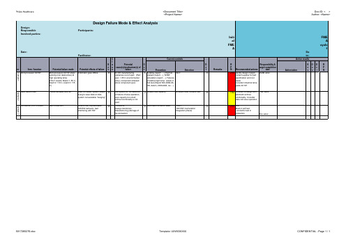
functionality, Consider
state call save operation
PMe, wkxx
200 -DfA
-Built-in self test
- connector test in
production
RdJ, wkxx
Doc-ID: < > Author: <Name>
Da te:
Action results
FME A
cycle 1
Action taken
SOD
R
ece
P
vc t
N
5017265276.xlsx
Template: UXW030XXX
CONFIDENTIAL - Page 1 / 1
interfacing with SW
-Manufacturing (damage of
(integration phase)
the connector)
Remarks
Initi al
FME A
R
Responsibility &
P
target completion
N Recommended actions
e
Potential failure mode
Potential effects of failure v s
failure
c
Prevention
Detection
t
Microprocessor XC167 stops Collimator goes offline
8 XC167 manufacturing
测试规范

√
√
√
6.2 Electrical(derating) test(使用率测试)
√
√
6.3 Input Chatter/(on off) test(输入开、关测试)
√
√
√
√
6.4 Component Open/Short test(组件开、短路测试)
√
√
7 Others其它
7.1 2K Hours Life Test(两千小时寿命测试)
√
√
4.4 High Temperature Operating test(高温操作测试)
√
√
√
4.5 Low Temperature Operating test(低温操作测试)
√
√
√
4.6 Waterproof test(防水测试)
5 Reliability Prediction test(可靠性预估测试)
√
√
√
3.3 Low Temperature test低温电性测试
√
√
√
4 Environmental test (环境测试)
4.1 High Humidity storage test(高湿存储测试)
√
√
√
4.2 High Humidity Operation test(高湿操作测试)
√
√
√
4.3 Thermal Shock test (冷热冲击测试)
2.5 Packaged drop test(包装跌落测试)
√
√
2.6 Unpackaged drop test(裸机跌落测试)
√
√
√
√
2SC2383中文资料(toshiba)中文数据手册「EasyDatasheet - 矽搜」

(V)
0.1
Collector-emitter saturation voltage
CE (sat)
IC/IB = 10
V 0.05
5 0.03
0.01
5 10
30
100
300
1000
Collector current I C (mA)
VCE (sat) – IC
0.5
Common emitter 0.3 IC/IB = 10
• 产品适用于一般电子应用(如电脑,个人设备,办公设备,测量设备,工业机器人和家用电子电器)或特定的应用,明确本文中提到的使用.
产品既不打算,也没有必要使用设备或需要非常高水平的质量和/或可靠性和/或故障或失败的系统,其中可能造成的生命损失,人身伤害,重大财产损 失或严重的公众影响( “误用”).非预期使用包括,但不限于核设施使用的设备,在航空航天工业中使用的设备,医疗设备,用于汽车,火车,轮船 等运输,交通信号设备,用于控制发火或爆炸装置,安全装置的设备,电梯和自动扶梯,涉及到电力设备,以及设备在金融相关领域.不要使用产品的 误用,除非本文档中的特别许可.
0.005
3
10
30
100
300
Collector-emitter voltage V CE (V)
4
2009-12-21
芯片中文手册,看全文,戳
2SC2383
限制产品用途
• 东芝公司及其子公司和附属公司(统称为“TOSHIBA”),保留对本文档的更改信息的权利,以及相关的硬件,软件和系统(统称为“产品”),恕不另行通 知.
1 ms* 10 ms*
0.1 Collector current I
LV215-VW_80302 -2013 德国大众高压测试标准

Group standardVW 80302Issue 2013-03Class. No.:8ME2Descriptors:high-voltage contacts, high-voltage, contacts, Test Specification, LV 215-2Motor Vehicle High-Voltage Contacts Test SpecificationPrefaceThis standard is based on LV 215-2, which was drawn up by representatives of automobile manu‐facturers Audi AG, BMW AG, Daimler AG, Porsche AG, and Volkswagen AG in working group (WG) 4.3.3.Deviations from the LV 215-2 are listed on the cover sheet of this standard. If modifications to indi‐vidual test sections become necessary in individual cases, these must be agreed upon separately between the department in charge and the relevant manufacturer.Test reports will be accepted as long as the tests were performed by an independent testing insti‐tute that is accredited as per DIN EN ISO/IEC 17025. Acceptance of the test reports will not auto‐matically result in a release.NOTE 1: The LV numbers listed in this document correspond to the standards listed in table 1.Table 1Working group (AK) document numberLV 214LV 215-1LV 216-1LV 216-2Volkswagen standard numberVW 75174VW 80304VW 75210-1VW 75210-2Previous issuesVW 80302: 2009-09, 2013-02ChangesThe following changes have been made to VW 80302: 2013-02:–Page 13 replacedAlways use the latest version of this standard.This electronically generated standard is authentic and valid without signature.The English translation is believed to be accurate. In case of discrepancies, the German version is alone authoritative and controlling.Numerical notation acc. to ISO/IEC Directives, Part 2.Page 1 of 13All rights reserved. No part of this document may be provided to third parties or reproduced without the prior consent of one of the Volkswagen Group’s Standards departments.© Volkswagen AktiengesellschaftVWNORM-2012-05oPage 2LV 215-2: 2013-02ContentsPage Test number structure (3)Loads (3)Properties tests (3)General rules (3)Determining the volume resistance (E 0.2, E 14.0, and E 16.0) (3)"Crimp" definition (3)PG 0Inspection of as-received condition (4)PG 1Dimensions (5)PG 2Material and surface analysis, contacts (5)PG 3Material and surface analysis, housing and single-wire seal (5)PG 4Contact overlap (6)PG 5Mechanical and thermal relaxation behavior (6)PG 6Interaction between contact and housing (6)PG 7Handling and functional reliability of the housing (6)PG 8Insertion and retention forces of the contact parts in the housing (7)PG 9Pin insertion inclination/misuse safe (scoop-proofing) (7)PG 10Contacts: Conductor pull-out strength (7)PG 11Contacts: Insertion and withdrawal forces; insertion frequency (7)PG 12Current heating, derating (8)PG 13Housing influence on the derating (8)PG 14Thermal time constant (current vs. temperature at n-times the nominal current) (8)PG 15Electrical stress test (8)PG 16Friction corrosion (8)PG 17Dynamic load (8)PG 18A Coastal climate load (9)PG 18C De-icing salt load (9)PG 19Environmental simulation (9)PG 20Climate load of the housing (9)PG 21 Long-term temperature aging (9)PG 22A Chemical resistance (9)PG 22B Chemical resistance, extended test (9)PG 23Water leak tightness (9)PG 24Impenetrability to paint (9)PG 28Latching noise (10)PG 29Blind plug retention force (10)PG 50EMC test (10)PG 51Protection against contact (12)Page 3LV 215-2: 2013-02 Test number structureAs per LV 214LoadsAs per LV 214Properties testsAs per LV 214As a supplement to LV 214:E 0.2.3 Shielding volume resistanceE 0.3 Insulation resistanceE 0.4 Dielectric strengthE 50.1 Average wave impedance DIN EN 50289-1-11E 50.2 Surface transfer impedance VG 95214-11E 51.1 Protection against contact ISO 20653General rulesAs per LV 214As a supplement to LV 214:Only cables released as per LV 216-1/LV 216-2 must be used for high-voltage contacts.This LV is an extension to LV 214.If modifications to individual test sections become necessary in individual cases, these must be agreed upon separately between the appropriate department and the affected manufacturer.In general: All tests in LV 214 are described as connector tests and must be conceptually appliedto threaded connections.Determining the volume resistance (E 0.2, E 14.0, and E 16.0)As per LV 214Deviation: starting from class 4, measure the volume resistance as per DIN EN 60512-2-2 with a test current of 10 A."Crimp" definitionAs per LV 214Page 4LV 215-2: 2013-02PG 0 Inspection of as-received conditionAs per LV 214As a supplement to LV 214:E 0.2.3 Shielding volume resistance, measuring method as per E 0.2 (transition from componentto cable shield)Document the exact position of the measuring points.Requirement:The measured values must correspond to the manufacturer’s specifications. The limits for R1 and R2 must be adhered to (see LV 215-1) and the measured values (initial value, standard deviation for the corresponding specimens) must be documented accordingly in the test report. Limit R3 (see LV 215-1) must be adhered to and must be checked during the release tests for the component, since the actual material combinations will only be available at that point.R1 = DC resistance between cable shield and connector shieldR2 = DC resistance between connector shield and interface shieldR3 = DC resistance between interface shield and unitE 0.3 Insulation resistanceIn addition, measure the insulation resistance between the contacts and the housing shielding.Requirement:R insul >200 megaohms with V = 1 000 VDC, t = 60 sE 0.4 Dielectric strength (one-time test) SAE J1742ISO 6469-3 with a test duration of 60 seconds and a leakage current <10 mA.The test voltage must be selected from Table 1.Page 5LV 215-2: 2013-02Table 1: Test voltagesRMS voltage connector AC voltage to beapplied(RMS)DC voltage to beapplied 50 – 100 V 1 000 V 1 600 V 110 – 300 V 1 600 V2 500 V300 – 1 000 V1 000 V plus2 times the connector's nominal voltage 1 600 V plus 3,2 times the connector's nominal voltageFigure 1: Test setup Housing insulation:Connect all circuits to each other (see Figure 1) and wrap the outside of the specimen inconductive film.Apply the test voltage between the film and the circuits for one minute. Document the results.Conductor insulation:Test each conductor individually by using the shield as the other reference point. Apply the test voltage between the conductors and the shield for one minute. Document the results.Requirement:During the test, no dielectric breakdown or flash-overs must occur between the individual chambers or between the chambers and the specimen's exterior.PG 1 Dimensions As per LV 214PG 2 Material and surface analysis, contacts As per LV 214PG 3 Material and surface analysis, housing and single-wire sealAs per LV 214As a supplement to LV 214:Page 6LV 215-2: 2013-02E 3.1 Material test of housing and single-wire seal…•D o c u m e n t a t i o n o f t h e m a t e r i a l s:o C r e e p a g e c u r r e n t c l a s s i f i c a t i o n(C T I v a l u e s)…PG 4 Contact overlapAs per LV 214PG 5 Mechanical and thermal relaxation behaviorAs per LV 214 for HV contactsTest the shield contact with a suitable method for measuring the contact normal force.The following applies to HV threaded connections:The screw assembly for the housing and tubular cable lug must be designed as appropriate for the component and checked during the release tests for the component, since the actual material combinations will only be available at that point.PG 6 Interaction between contact and housingAs per LV 214Deviating from LV 214:B 6.1 Drop test (with new housings; see batch size) as per DIN EN 60068-2-31, free fall as permethod 1Test setup:Housing fully populated with max. cable cross-sectional area; cable length: 500 mm; drop height: 1 mRequirement:There must not be any discernible broken parts or any damage that will have a negative impact on suitability of usePG 7 Handling and functional reliability of the housingAs per LV 214As a supplement to LV 214:Page 7LV 215-2: 2013-02Table 3 as per LV 214: Positive-locking housing retention forcesP o s i t i v e-l o c k i n g h o u s i n g r e t e n t i o n f o r c e s(N)C o n t a c t s i z e N u m b e r o f p i n s1-p i n t o2-p i n3-p i n t o6-p i n>6-p i n0,63t o1,2m m>60>80>100>1,2t o2,8m m>80>100>100>2,8t o6,3m m>100>100>100>6,3m m>150>150>150≥8m m>250>500PG 8 Insertion and retention forces of the contact parts in the housingAs per LV 214, provided the design allows for the contact parts to be removed.The values for ≥8 mm apply to class 4 with a locking barb. Preferably, test them directly on the contact with a push-out test.PG 9 Pin insertion inclination/misuse safe (scoop-proofing)As per LV 214PG 10 Contacts: Conductor pull-out strengthAs per LV 214As a supplement to LV 214:Requirement:The conductor pull-out strengths as per LV 215-1 must be adhered to.PG 11 Contacts: Insertion and withdrawal forces; insertion frequencyAs per LV 214The following applies to HV threaded connections:B 11.1 Insert and disconnect the specimens according to their surface finish. The followingtightening torques (±10%) apply to threaded electrical connections:M6 9 NmM8 15 NmM10 25 NmRequirement:It is impermissible for the contact surface required for proper operation to be worn all the way through to the base material or barrier layer. Corresponding documentation must be provided.Page 8LV 215-2: 2013-02E 11.2 Retention force of protection-against-contact elementUse a suitable device to try to pull the protection-against-contact element.Requirement:Verify that the protection-against-contact element can handle twice the pull-out force of the socket contact against the insertion direction and, if there are installed elements, against the installation direction of the protection-against-contact cap. The force that the protection-against-contact element can handle must be at least 50 N if the aforementioned withdrawing force times two is lesser.PG 12 Current heating, deratingAs per LV 214As per E 0.1, measure and document the contact resistances as per E 0.2 as well.PG 13 Housing influence on the deratingAs per LV 214As a supplement to LV 214:Plot derating curves with a 10-A shield current as well.PG 14 Thermal time constant (current vs. temperature at n-times the nominal current) As per LV 214Plot the cool-down curve in addition to the heat-up time constant.PG 15 Electrical stress testAs per LV 214As a supplement to LV 214 as per E 0.2:E 0.2.3 Shield contact resistanceThe following applies to HV threaded connections:B 15.1 Insert and disconnect the specimens 2 times.PG 16 Friction corrosionAs per LV 214, following consultationPG 17 Dynamic loadAs per LV 214Vibration profile as per severity 3Temperature profile as per severity 4As a supplement to LV 214 as per E 0.2:E 0.2.3 Shield contact resistancePage 9LV 215-2: 2013-02PG 18A Coastal climate loadAs per LV 214As a supplement to LV 214 as per E 0.2:E 0.2.3 Shield contact resistancePG 18C De-icing salt loadAs per LV 214Metal housings must meet additional OEM-specific requirements (OEM – original equipment manufacturer).PG 19 Environmental simulationAs per LV 214As a supplement to LV 214 as per E 0.2:E 0.2.3 Shield contact resistancePG 20 Climate load of the housingAs per LV 214PG 21 Long-term temperature agingAs per LV 214As a supplement to LV 214 as per E 0.2:E 0.2.3 Shield contact resistancePG 22A Chemical resistanceOmittedPG 22B Chemical resistance, extended testAs per LV 214PG 23 Water leak tightnessDeviation:Open cable endsTest: B 23.3 Thermal shockPG 24 Impenetrability to paintFollowing consultationPage 10LV 215-2: 2013-02PG 28 Latching noiseAs per LV 214PG 29 Blind plug retention forceAs per LV 214, provided they are included in the designPG 50 EMC testPurpose: Measurement of the effectiveness of the housing shielding or the surface transfer impedance.Batch size: 3 housingsContact parts: A ll variants, conductor cross-sectional areas, and surfaces Housing:All variants; any keying and colorType of test:E 50.1 Average wave impedanceDIN EN 50289-1-11Determine the average wave impedance of the bulk cable with the capacitance and service life as per DIN EN 50289-1-11E 50.2 Surface transfer impedanceVG 95214-11Conduct the test, based on VG 95214-11, within a frequency range of 100 kHz to 500 MHz. Measure the difference between a reference cable (bulk) and a finished cable. The specimen's total length is (1 000 ±100) mm from the terminal resistor 3R to the receiver connection (see Figure 2).Measuring setup and coupling cable: VG 95214-11 describes the test setup.The DC resistance between the measuring contact systems, on both sides of the specimen, that connect the equipment under test (EUT) and the measuring adapters must not be more than 10% greater than the measured shield resistance of the EUT without the measuring contact systems.As the terminal resistance for the specimen, use the asymptotic wave impedance value that results at high frequencies as per E 50.1. Terminal resistances 0R and 3R must be suitable for high frequencies throughout the entire frequency range. Note:Carbon film and wire-wound resistors must not be used. A reflection measurement on the network analyzer (NWA) can be carried out on the resistors in order to check their frequency stability. Insert the resistors into an N connector for this purpose. The reflection factor can be improved by connecting several SMD resistors in parallel.The entire measuring setup must be insulated (do not use a ground plane). The NWA provides the reference ground. Ensure that there are no metallic objects in the vicinity of the setup (minimum clearance: 20 cm).Page 11LV 215-2: 2013-02 The coupling characteristics must not change during the measurement. For this purpose, the supply cable in particular must be secured in such a way that there is continuous contact between the supply cable and the specimen.The supply cable's reflection factor must be up to 30 MHz <20 dB and up to 110 MHz <10 dB.Perform the measurement at the receiver and sender with a system impedance of 50 Ω. Any impedance mismatch must not be corrected. In particular, this means that impedance matching circuits, as well as the NWA's port Z conversion function, must not be used. (This is to prevent the measured result from depending on the quality of the impedance matching circuit setup or from conversion algorithms by different NWA manufacturers.) Measurement:Carry out the measurement with the "far-end" configuration.Measure the difference between a reference cable and a cable terminated on one end. The cable terminated on one end consists of the reference cable and the high-voltage contact system being evaluated. Use a released high-voltage cable as per LV 216-2 as the reference cable. The chosen cable's cross-sectional area must match the connector's permissible cross-sectional area.In the case of multicore cables, connect the insulated wires in parallel if a common shield is used. In the case of contact systems with multiple shielded individual cables that use a common contact carrier, consult with the EMC department to determine whether the individual cables need to be measured separately or whether a combined measurement with all the shields needs to be performed.Perform the measurement at three or four positions within the specimen's perimeter. For this purpose, turn the specimen 120° or 90° relative to the supply cable. Ensure that the supply cable is carefully secured and impedance-matched for every measurement.Figure 2: Parallel wire method setupUse "OSL" (open-short load) and "Thru" as the calibration methods.Perform the measurements from 100 kHz to 500 MHz.Page 12LV 215-2: 2013-02Evaluation:The surface transfer impedance (T Z ) must be calculated for the evaluation. Use the formula in VG 95214-11 to convert the measured coupling attenuation T A to surface transfer impedance T Z :20302T T10A l R R Z ⋅⋅⋅=T Z Surface transfer impedance in m Ω/ml Specimen coupling length (as per figure 2: 500 mm)0R Supply wire terminal resistance (50 Ω)3R Specimen terminal resistance (the DUT's average wave impedance)T A Measured level on network analyzer/voltage ratio, in dB, between measuringreceiver and measuring sender.Document the values used as per the formula.For each specimen, show all the measurements for the angles in a single diagram in the test report.For all measurements, show the information related to determining the supply cable reflection factor as necessary for the measurement in the test report.Requirement:The limits must be adhered to (see LV 215-1)The target data must be defined in coordination with the pertinent manufacturer or must comply with the pertinent OEM Performance Specification.PG 51 Protection against contactGoal:Verifying that protection against contact works properlyBatch size:1 housing Contact parts:A ll variants, largest conductor cross section, and any surface Housing:All variants; any keying and colorType of test: E 51.1 Protection against contact ISO 20653Press the access probe against every opening on the housing using the force specified in Table 2. If it penetrates partially or completely, it is moved into every possible position. However, the locating surface must not go completely through the opening under any circumstances.Possible mechanical parts must be moved slowly during the test.Page 13LV 215-2: 2013-02Signal circuit method:When performing tests on low-voltage operating equipment, a low-voltage power source (not lower than 40 V and not higher than 50 V) must be connected in series with a suitable lamp between the probe and the hazardous parts inside the housing.Table 2: Test finger access probeRequirement:A fully assembled HV connector system must have an IPXXD degree of protection.A non-fully assembled HV connector system must have an IPXXB degree of protection. The access probe must not come into contact with hazardous (live) parts.The lamp must not turn on in the signal circuit method.No measurable voltage or arcing must occur during the high-voltage test.。
工厂自测无故障运行报告范文

工厂自测无故障运行报告范文英文回答:Factory Self-Test Report on Fault-Free Operation.Introduction:I am pleased to present the self-test report on thefault-free operation of our factory. This report aims to provide an overview of the testing process, the results obtained, and the measures taken to ensure the smooth functioning of our factory.Testing Process:To ensure the accuracy and reliability of the self-test, we followed a systematic approach. First, we conducted a thorough inspection of all machinery and equipment in the factory. This involved checking for any signs of wear and tear, loose connections, or malfunctioning parts.Additionally, we tested the performance of each machine to ensure it met the required standards.Results:I am delighted to report that our factory has successfully passed the self-test without any identified faults. All the machinery and equipment performed exceptionally well, meeting or exceeding the expected benchmarks. This outcome is a testament to the high-quality maintenance and diligent efforts of our team.Measures Taken:To maintain the fault-free operation of our factory, we have implemented several measures. Regular maintenance schedules have been established to ensure all machinery and equipment are inspected and serviced at appropriate intervals. Any signs of wear and tear or potential issues are promptly addressed to prevent any disruptions to our production process.Furthermore, we have invested in the training and development of our staff to enhance their technical skills and knowledge. This enables them to troubleshoot and resolve any minor issues that may arise, minimizing therisk of major faults.Conclusion:In conclusion, our factory has successfully undergone the self-test process and has been found to operate without any identified faults. This achievement is a result of our commitment to regular maintenance, diligent inspections, and continuous staff training. We will continue toprioritize the smooth functioning of our factory to ensure the highest quality production and customer satisfaction.中文回答:工厂自测无故障运行报告。
元件使用率测试工作指引

德信诚培训网
更多免费资料下载请进: 好好学习社区
元件使用率測試工作指引
1. 目的 /Objective
元件使用率的測試是檢查元件在不同的測試條件下﹐實際使用電壓﹑電流和功率跟其額定值的比值﹐這是確保產品沒有由于元件超出使用范圍而引起損壞。
Component derating test is to check the ratio of actual voltage, current and power applied to a component against their rated value under various test conditions. This is to ensure that no component is overstressed which may cause failure of the product.
2. 范圍 /Scope
適用于柏怡電子廠開發的所有產品。
Applicable to all products developed by PI Electronics.
3. 使用儀器 /Main equipment
● 在工程樣板1(EVT)和工程樣板2(DVT)階段﹐所有元件均必須測試。
● 數字存儲示波器 /Storage oscilloscope
● 數字萬用表 /DVM
● 電子負載 /Electronic load
● 有效值數字表 /RMS meter
●
電流探頭 /Current probe 4. 步驟 /Procedure
4.1 使用率測試覆蓋范圍 /Test coverage
● 在工程樣板1(EVT)和工程樣板2(DVT)階段﹐所有元件均必須測試。
电解电容纹波及寿命测试方法
Electrolytic Capacitor Ripple Current Derating Test Method and Life Time EvaluationFrom:郭雪松Date:Oct-27-04 一.SPEC1.电解电容零件工程规格书中之Standard Rating表格,其中规定了不同规格的电解电容Rated Ripple Current值,例如:Sharp机种PWPC C904(滤波电容) 67L215L-820-15N (CNN公司KXG Series)2.此电容用于电源输入端滤波,因此采用120Hz时的Rated Ripple Current规格715mA。
3.而用于评估电解电容Ripple Current之Spec要依据以下公式:SPEC=Spec(component)×频率系数(FM)×温度系数(TM)注:FM/TM取值方法见附表4.OTPV 评估电解电容Ripple Current的Derating规格为85%,因此测试值<SPEC×85%时判定OK。
二.Test Method将电解电容接地端吸开串联一导线,直接用电流计探头测试该导线电流的有效值(rms),测试时要调整输入电压值(90V~264V)达到纹波电流最大。
见图示:Irms三.附表(FM&TM取值方法):NCC公司产品为例1.Multiplying Factors on KMG Series(radial lead type)Frequency MultipliersTemperature Multipliers2. Multiplying Factors on KY SeriesFrequency MultipliersTemperature Multipliers3. Multiplying Factors on KXG SeriesFrequency MultipliersTemperature Multipliers*Temperature multipliers shows the guide limits of the maximum available ripple current at each of the temperature,of which the life time at the rated maximum operating temperature is expected.四.电解电容寿命评估测试方法1.Calculation Formula:电容寿命Life Time= Life(spec)×2(Ts-Tt)/10Life(spec):指spec中标明的寿命值Ts:电容最高使用温度值Tt:电容本体温度测试值2.判定方法:以上计算得出之寿命值与整机MTBF目标值比较,若大于目标值则判定OK。
计算机专业常用英语词汇总结

计算机专业常用英语词汇总结计算机专业英语词汇指与计算机硬件、软件、网络等多方面有关的英语词汇,主要包括硬件基础、计算机系统维护、计算机网络基础、软件、程序设计语言、计算机网络技术、IT职场英语等词汇。
店铺为大家总结一些计算机常用词汇:compilation 编辑compilation time 编译时间compilation unit 编译单位compilc 编译compile 编辑compile and go 编译及执行compile phase 编译时间compile time 编译时间compile, machine language 机器语言编译compile-time error 编译时期错误compiled resource file 编译资源文件compilei 编译器compiler 编译器compiler defect report 编译器缺失报告compiler diagnostcs 编译程序侦断compiler directive 编译程序定向compiler generatoi 编译程序产生器compiler interface 编译器界面compiler language 编译器语言compiler manager 偏译器经理compiler options 编译器任选compiler vs. interpreter 编译器对编译器compiler, cobol cobol编译器compiler-complier 编译程序的编译程序compilers 编译器compiling duration 编译期间compiling routine 编译例程compiling time 编译时间complement base 互补基点complement instruction 补码指令complement on n n补码complement on n-1 n-1补码complement, diminished 减少补码complement, nines 九补码complement, noughts 0补码complement, ones 1补码complement, tens 10补码complement, two 2补码complementary 补色complementary bipolar ic 互补双极集成电路complementary metal oxide semiconductor (cmos) 互补式金氧半导体complementary mos(cmos) 互补金属氧化半导体complementary operation 互补运算complementary operations 互补运算complementary operator 互补运算子complementary scr(cscr) 互补硅控整流器complementei 补码器complementing 互补complete carry 完全进位complete object 终衍物件complete operation 完全作业complete routine 完全例程completeness 完整性completeness check 完整检查completeness errors (remote computing sy) 完成误差completion code 整体码complex bipolai 复合双极complex constant 复合常数complex data 复合贫籵complex decision-making simulation 复合决策模拟complex instruction set computer (cisc) 复杂指令集计算机complex instruction set computing (cisc) 复杂指令运算complex number 复数complex relocatable expression 复数可重置表示法complex script 复杂脚本complex-bound 复杂系结compliant 相容compliant naming 适用的名称compnter, first generation 第一代计算器component 组件component address 组件地址component code generator 组件程序代码产生器component density 组件密度component derating 分件降低定额component erroi 组件误差component fail impact analysis, cfia 组件失误撞击分析component gallery 组件展示廊component load balancing 组件负载平衡component name 组件名称component object 组件对象component object model 组件对象模型 (com) component object model (com) 组件对象模型component project 组件项目component registrar 组件登录器component selector 组件选取器component services explorer 组件服务总管component site 组件站台component software 组件软件component stress 组件应力component tray 组件匣component video 成分视讯component wizard 组件精灵component, solide-state 固态组件component-based development 组件式软件开发技术compose 撰写compose buffer 撰写缓冲区composite 合成composite black 合成黑色composite cable 复成电境composite conductoi 复合导体composite console 复合控制台composite control 复合控件composite data servicevendoi 复合数据服务贩责者composite display 合成屏幕composite filter 复合滤波器composite module data set 复合模块数据集composite module library 复合模块数据馆composite modules 复合模块composite moniker 复合型composite operator 复合运算子composite video 复合视讯composite video input 复合视讯输入composited circuit 复成电路compositing 复合composition error 组合误差composition file 复合档composition video signal 复合视频信号compound condition 复合条件compound document 复合文件compound document files 复合文件档案compound file 复合档案compound logical element 多逻辑组件compound-assignment operator 复合设定运算子compoundstatement 复合叙述compress 压缩compressed files 压缩档compressed serial link internet protocol, compressed slip 压缩式串连链接因特网协议compressed video vs. facsimile 压缩视频对传真compression 压缩方式compression algorithm 压缩算法compression format 压缩格式compression scheme 压缩方法compression, data 数据压缩compression, zero 零压缩compression/decompression (codec) 编码/译码compressor 压缩器compromise net 协调网络computation, address 地址计算computation, implicit 隐含计算computational stability 计算稳定度computcr-aided dispatch(cad) 计算器辅助发送compute 运算compute mode 计算型computer 计算机;计算器computer & communications research labs (itri) 工研院计算机与通讯工业研究所computer administrative records 计算器管理记录computer aided logistic support (cals) 计算机辅助后勤支持系统computer aided software engineering (case) 计算机辅助软件工程computer animation 计算器电影制作computer application 电脑应用系统computer architecture 电脑体系结构computer bureau 电脑服务中心computer capacity 计算器容量computer cartography 计算器制图法computer center 电脑中心computer center manager 计算器中心管理人computer circuits 计算器电路computer communications 计算机通信computer communications system 计算器通信系统computer conferencing 电子计算器会议computer configuration 计算器组态computer configuration 计算器组态computer console 计算器控制台computer control 计算器控制computer duplex 计算器双工computer emergency response team 电脑紧急应变小组computer equation 计算器方程式computer equipment operation 电脑设备操作computer generated image (imagery, cgi) 计算机产生的影像computer graphics (cg) 计算机图形;计算器制图法computer graphics (cg) 计算器制图法computer graphics interface (cgi) 计算机图形接口computer graphics technology 计算器制图法技术computer image processing 计算器影像处理computer installation (service) 安装计算机 [ 服务 ]computer instruction 计算器指令computer instruction code 计算器指令码computer instruction code 计算器指令码computer instruction set 计算器指令集computer integrated manufacturing (cim) 计算机整合制造computer interface types 计算器分界面类型computer interface unit (ciu) 计算器界面单位computer language 计算器语言computer language symbols 计算器语言符号computer learning 计算器学习computer letter 计算器信件computer logic 计算器逻辑computer memory 计算机内存computer micrographics 计算器微图形computer name 计算机名称computer network 电脑网络computer network components 计算器网络组件computer numerical control 计算器数值控制computer operating procedures manual 电脑操作程序手册computer operation 计算器运算computer operator 电脑操作员computer output microfilm (com) 计算器输出微胶片computer output microfiche 电脑输出缩微胶片computer output microfilm 电脑输出缩微胶卷computer output microfilmer (com) 计算器输出微影机computer output microform 电脑输出缩微方式computer peripherals 计算器外围设备computer power center (cpc) 计算机动力中心computer program 电脑程式computer program origin 计算器程序原始computer programming language 计算器程序语言computer project 电脑计划computer readable medium 电脑可读媒体computer scicnccs (cs) 计算器科学computer service level requirement 电脑服务水平要求computer service orsanization 计算器服务组织computer simulatoi 计算器仿真器computer site preparation 电脑场地准备工作computer storage 计算器储存器computer stores 计算器商店computer system 电脑系统computer system audit 计算器系统审计computer telephony integration (cti) 计算机语音整合computer terminal 电脑终端机computer time 计算器时间computer utility 计算器公用computer virus 电脑病毒computer vision 计算机视觉computer word 计算器字computer-aided design & drafting (cadd) 计算机辅助设计与绘图computer-aided design (cad) 计算机辅助设计computer-aided education (cae) 电脑辅助教育computer-aided engineering (cae) 计算机辅助工程computer-aided experiment (cae) 计算机辅助实验computer-aided instruction (cai) 计算机辅助教学computer-aided manufacturing (cam) 计算机辅助制造computer-aided publishing 电脑辅助出版computer-aided test (cat) 计算机辅助测试computer-assisted learning (cal)计算机辅助学习computer-assisted management 计算器辅助管理computer-assisted publishing 电脑辅助出版computer-assisted software engineering tool 计算机辅助软件工程工具computer-assisted typesetting 电脑辅助排字computer-based automation (cba) 计算器基准自动化computer-based training (cbt) 计算机辅助训练computer-controlled pattern generator 计算器控制型样产生器computer-generated (cg) 计算机合成的computer-generated map 计算器产生地图computer-independent language 计算器通用语言computer-integrated manufacturing (cim) 计算机整合制造computer-mediated communication (cmc) 计算机媒介沟通;计算机中介传播(沟通)computer-operated memory test system 计算器运算记忆测试系统computer-oriented language 机向语言computerarchitecture 计算机结构computerese 计算机文computerization 电脑化computerization requirement 电脑化需求computerization strategy 电脑化策略computerized foreman 计算机化领班computerized hyphenation 计算机化忠诚computerized numerical control (cnc) 计算机化数字控制computerized patient record (cpr) 电子病历computerized tomography 计算机化断层摄影术computer、communication、consumer electronics (3c) 3c多元化技术整合computex computexcomputing 计算computing amplifier 计算放大器computing element 计算组件computing machinery 计算器械computing power 计算能力computing, multiaccess 多重接达计算computor, sensor-based 传感器为基础的系统comsat 通信卫星con 主控台concatenate 序连concatenate data set 序连资料集concatenated key 串连索引键concatenation 序连concatenation character 序连字符concatenation operator 串连运算子concentrated messages 集中信息concentration 集中concentration, data 资料集中concentrator terminal buffer(ctb) 集讯器终端机缓冲器concept coordination 概念协调conceptual data model 概念数据模型conceptual infrastructure 概念基本建设conceptual level 概念级conceptual modei 概念模式conceptual model 概念模型conceptual modeling 概念模拟conceptual schema 概念模式conceptual system design 概念系统设计concert 音乐会concordance 索引concordance program 索引程序concordant 调和排列concrete 具象的concrete syntax 具体语法concrete syntax of sgml sgml的具体语法concrete syntax parameter 具体语法参数concurrcnt 同作concurrency 并行性concurrency mode 同作模态concurrency, executive-system 执行系统同作concurrency, operations(real-time) 实时同作操作concurrency, real-time 实时同作concurrent connections 同时联机concurrent i/o 同作输出入concurrent operating control 同作作业控制concurrent operation 同作运算concurrent processing 同作处理concurrent real-time processing 同作实时处理concurrent/concurrency 并行。
减额降额测试规范Derating_Test_Procedure

减额降额测试规范Derating Test Procedure1.0 PURPOSE:(目的):1.1 这个测试的目的是在确认所生产的产品其所使用的零件材料,当产品在正常操作下其各零件的电压、电流、功率是否在额定操作规格范围内,以防止电子零件因选用不当所造成电气或安全上的损坏。
2.0 SCOPE:(范围):2.1 凡是在所生产的产品须经过此测试。
3.0 SPECIFICATIONS:(规格):3.1 在任何测试过程中或测试完成阶段,待测物(电子零件)的电气参数,都须符合公司内部所订定的元作减额定规范。
备注:电子零件的各电气最大额定操作规格以各厂牌Data book所规定为主。
4.0 TEST EQUIPMENT:(测试设备):4.1 电子负载4.2 数位电表4.3 变频器4.4 示波器5.0 CONDITION S:(测试条件):5.1 AC输入电压:90Vac / 264Vac5.2 输出负载:全载5.3 环境温度:室温6.0 TEST PROCEDURE:(测试步骤) :6.1参阅电路图依各元作所在位置或其所担负的工作,选定主要组件为优先测试对象,其余的则视主客观需求而执行。
6.2 将待测物连接到电源、电子负载,并将示波器的探针连接到欲量测之电子零件,然后开启AC电源。
备注:需在90Vac and 264Vac电源和满载条件下执行这项测试,或依客户规格执行测试。
6.3 待测物电气稳定后,观察示波器所显示之电气参数,并将其最大值纪录于Derating Test Report中。
6.4 关闭AC电源,变换AC电压或变换欲量测之电子零件或更换测试之电气参数后,开启待测物电源,再重复步骤 6.2及 6.3。
6.5如有超出各项减额定规格者,须列出并通知产品设计者要求其改善,改善后须重新送件并附上测试报告,以为再次确认之依据。
7.0 ACCEPTANCE CRITERIA:(判定):7.1在任何测试过程中或测试完成阶段,待测物之各电气参数均需在该电子零件最大操作规格的95%下正常操作,且不应有任何不稳动作且性能降低情形发生。