ne555dr中文资料
完整版NE555中文资料

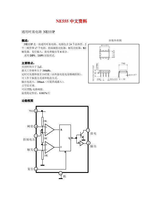
NE555中文资料通用时基电路NE555P概述:封装外形图NE555P是一块通用时基电路,电路包含24个晶体管,2 个二极管和17个电阻,组成阈值比较器,触发比较器,RS 触发器,复位输入,放电和输出等6部分。
采用DIP8、S0P8封装形式。
主要特点:关闭时间小于2 S o最大工作频率大于500kHz。
定时可从微秒级至小时级(由外接电阻电容精确控制)可工作于振荡方式或单稳态方式。
输出电流大,200mA (可提供或灌入)。
占空比可调。
可同TTL电路相接。
温度稳定性好,0.005%/C功能框图极限值(绝对最大额定值,若无其它规定,Tamb=25C)(若无其它规定,Vcc=5~15V , Tamb=25应用图555芯片引脚图及引脚描述555的8脚是集成电路工作电压输入端,电压为5〜18V ,以UCC 表示;从分压器上看出,上比较器6脚A1的5脚接在 R1和R2之间,所以5脚的电压固定在 2UCC/3上;下比 较器A2接在R2与R3之间,A2的同相输入端电位被固定在 UCC/3上。
NE555管脚功能介绍:1脚为地。
2脚为触发输入端;3脚为输出端,输出的电平状态受触发器控制,而触发 器受上比较器6脚和下比较器2脚的控制。
当触发器接受上比较器 A1从R 脚输入的高电平时,触发器被置于复位状态, 3脚输出低电平;2脚和6脚是互补的,2脚只对低电平起作用,高电平对它不起作用,即电压小于1UCC/3 , 此时3脚输出高电平。
6脚为阈值端,只对高电平起作用,低电平对它不起作用,即输入 电 压大于2 Ucc/3,称高触发端,3脚输出低电平,但有一个先决条件,即 2脚电位必须大于1.单稳态延时电路V ;TVo -)丄工3.开机延迟电路:接通电源输岀Vo 由低跳变到高而延迟的电路。
延迟时间:td=1.1RCVo丄HFUAU o0. 01 uF 1 01WIH-O Vc c启动4.开机延迟电路:接通电源输岀 由高跳变到低而延迟的电路。
完整版NE555中文资料
NE555中文资料通用时基电路NE555P概述:封装外形图NE555P是一块通用时基电路,电路包含24个晶体管,2 个二极管和17个电阻,组成阈值比较器,触发比较器,RS 触发器,复位输入,放电和输出等6部分。
采用DIP8、S0P8封装形式。
主要特点:关闭时间小于2 S o最大工作频率大于500kHz。
定时可从微秒级至小时级(由外接电阻电容精确控制)可工作于振荡方式或单稳态方式。
输出电流大,200mA (可提供或灌入)。
占空比可调。
可同TTL电路相接。
温度稳定性好,0.005%/C功能框图极限值(绝对最大额定值,若无其它规定,Tamb=25C)(若无其它规定,Vcc=5~15V , Tamb=25应用图555芯片引脚图及引脚描述555的8脚是集成电路工作电压输入端,电压为5〜18V ,以UCC 表示;从分压器上看出,上比较器6脚A1的5脚接在 R1和R2之间,所以5脚的电压固定在 2UCC/3上;下比 较器A2接在R2与R3之间,A2的同相输入端电位被固定在 UCC/3上。
NE555管脚功能介绍:1脚为地。
2脚为触发输入端;3脚为输出端,输出的电平状态受触发器控制,而触发 器受上比较器6脚和下比较器2脚的控制。
当触发器接受上比较器 A1从R 脚输入的高电平时,触发器被置于复位状态, 3脚输出低电平;2脚和6脚是互补的,2脚只对低电平起作用,高电平对它不起作用,即电压小于1UCC/3 , 此时3脚输出高电平。
6脚为阈值端,只对高电平起作用,低电平对它不起作用,即输入 电 压大于2 Ucc/3,称高触发端,3脚输出低电平,但有一个先决条件,即 2脚电位必须大于1.单稳态延时电路V ;TVo -)丄工3.开机延迟电路:接通电源输岀Vo 由低跳变到高而延迟的电路。
延迟时间:td=1.1RCVo丄HFUAU o0. 01 uF 1 01WIH-O Vc c启动4.开机延迟电路:接通电源输岀 由高跳变到低而延迟的电路。
NE555DR;NE555PSR;NE555PWR;NE555D;NE555P;中文规格书,Datasheet资料

7 DISCH
Copyright © 1973–2010, Texas Instruments Incorporated
Submit Documentation Feedback
3
Product Folder Link(s): NA555 NE555 SA555 SE555
/
(1) Voltage levels shown are nominal.
2
Submit Documentation Feedback
Copyright © 1973–2010, Texas Instruments Incorporated
Product Folder Link(s): NA555 NE555 SA555 SE555
1
Please be aware that an important notice concerning availability, standard warranty, and use in critical applications of Texas Instruments semiconductor products and disclaimers thereto appears at the end of this data sheet.
NA555, NE555, SA555, SE555
SLFS022H – SEPTEMBER 1973 – REVISED JUNE 2010
Absolute Maximum Ratings(1)
over operating free-air temperature range (unless otherwise noted)
1
• Timing From Microseconds to Hours • Astable or Monostable Operation
NE555的详细介绍和引脚图

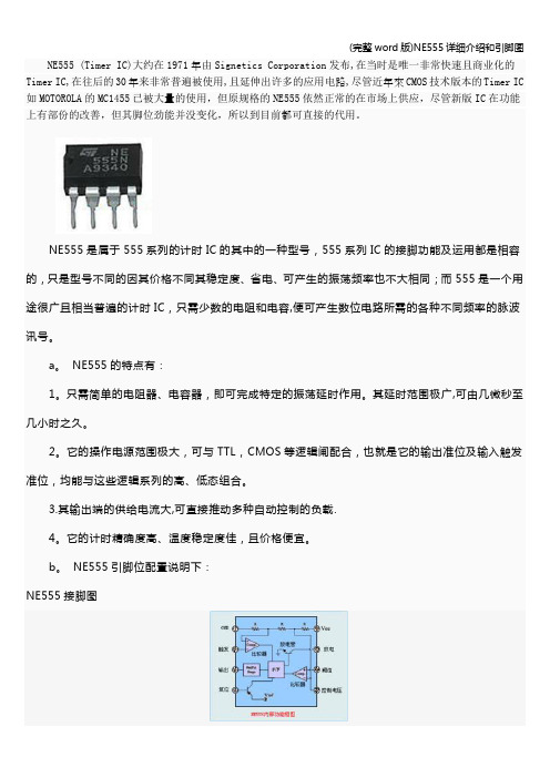
NE555的历史介绍NE555(TimerIC)大约在1971年由Si gneti cs Corpor ation发布,在当时是唯一非常快速且商业化的T imerIC,在往后的30年来非常普遍被使用,且延伸出许多的应用电路,尽C M OS技术版本的Ti mer IC如MOT OROLA的MC1455已被大量的使用,但原规格的N E555依管近年來然正常的在市场上供应,尽管新版IC在功能上有部份的改善,但其脚位劲能并没变化,所以到目前都可直接的代用。
NE555是属于555系列的计时IC的其中的一种型号,555系列I C的接脚功能及运用都是相容的,只是型号不同的因其价格不同其稳定度、省电、可产生的振荡频率也不大相同;而555是一个用途很广且相当普遍的计时IC,只需少数的电阻和电容,便可产生数位电路所需的各种不同频率的脉波讯号。
a. NE555的特点有:1.只需简单的电阻器、电容器,即可完成特定的振荡延时作用。
其延时范围极广,可由几微秒至几小时之久。
2.它的操作电源范围极大,可与TTL,CMOS等逻辑闸配合,也就是它的输出准位及输入触发准位,均能与这些逻辑系列的高、低态组合。
3.其输出端的供给电流大,可直接推动多种自动控制的负载。
4.它的计时精确度高、温度稳定度佳,且价格便宜。
b. NE555引脚位配置说明下:NE555接脚图ne555的结构图Pin 1 (接地) -地线(或共同接地),通常被连接到电路共同接地。
Pin 2 (触发点) -这个脚位是触发NE555使其启动它的时间周期。
触发信号上缘电压须大于2/3 VCC,下缘须低于1/3 VCC 。
Pin 3 (输出) -当时间周期开始555的输出输出脚位,移至比电源电压少1.7伏的高电位。
ne555中文资料 NE555使用介绍中文资料

ne555中文资料 NE555使用介绍中文资料导读:就爱阅读网友为您分享以下“NE555使用介绍中文资料”的资讯,希望对您有所帮助,感谢您对的支持!NE555中文资料2009-07-28 22:47ne555中文资料原理应用【如果资料对你有用,请顶一下~~】2009-04-16 19:47NE555绍NE555 (Timer IC)大约在1971年由Signetics Corporation发布,在当时是唯一非常快速且商业化的Timer IC,在往后的130年來非常普遍被使用,且延伸出许多的应用电路,尽管近年來CMOS技术版本的Timer IC如MOTOROLA的MC1455已被大量的使用,但原规格的NE555依然正常的在市场上供应,尽管新版IC在功能上有部份的改善,但其脚位劲能并没变化,所以到目前都可直接的代用。
NE555是属于555系列的计时IC的其中的一种型号,555系列IC的接脚功能及运用都是相容的,只是型号不同的因其价格不同其稳定度、省电、可产生的振荡频率也不大相同;而555是一个用途很广且相当普遍的计时IC,只需少数的电阻和电容,便可产生数位电路所需的各种不同频率之脉冲信号。
a. NE555的特点有:1.只需简单的电阻器、电容器,即可完成特定的振荡延时作用。
其延时范围极广,可由几微秒至几小时之久。
2.它的操作电源电压范围极大,可与TTL,CMOS等逻辑电路配合,也就是它的输出准位及输入触发准位,均能与这些逻辑系列的高、低态组合。
23.其输出端的供给电流大,可直接推动多种自动控制的负载。
4.它的计时精确度高、温度稳定度佳,且价格便宜。
5.静态电流最大值 VCC = 5 V, RL = ? =6mA VCC =15 V, RL = ? =15mA b. NE555引脚位功能配置说明下:图1-2 NE555各脚功能-管脚图 Pin 1 (接地) -地线(或共同接地) ,通常被连接到电路共同接地。
NE555中文资料【2】
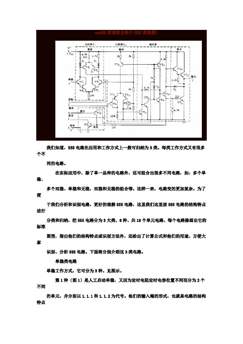
ne555原理图及例子(555原理图)我们知道,555电路在应用和工作方式上一般可归纳为3类。
每类工作方式又有很多个不同的电路。
在实际应用中,除了单一品种的电路外,还可组合出很多不同电路,如:多个单稳、多个双稳、单稳和无稳,双稳和无稳的组合等。
这样一来,电路变的更加复杂。
为了便于我们分析和识别电路,更好的理解555电路,这里我们这里按555电路的结构特点进行分类和归纳,把555电路分为3大类、8种、共18个单元电路。
每个电路除画出它的标准图型,指出他们的结构特点或识别方法外,还给出了计算公式和他们的用途。
方便大家识别、分析555电路。
下面将分别介绍这3类电路。
单稳类电路单稳工作方式,它可分为3种。
见图示。
第1种(图1)是人工启动单稳,又因为定时电阻定时电容位置不同而分为2个不同的单元,并分别以1.1.1和1.1.2为代号。
他们的输入端的形式,也就是电路的结构特点是:“RT-6.2-CT”和“CT-6.2-RT”。
单稳类电路单稳工作方式,它可分为3种。
见图示。
第1种(图1)是人工启动单稳,又因为定时电阻定时电容位置不同而分为2个不同的单元,并分别以1.1.1和1.1.2为代号。
他们的输入端的形式,也就是电路的结构特点是:“RT-6.2-CT”和“CT-6.2-RT”。
第2种(图2)是脉冲启动型单稳,也可以分为2个不同的单元。
他们的输入特点都是“RT-7.6-CT”,都是从2端输入。
1.2.1电路的2端不带任何元件,具有最简单的形式;1.2.2电路则带有一个RC微分电路。
第3种(图3)是压控振荡器。
单稳型压控振荡器电路有很多,都比较复杂。
为简单起见,我们只把它分为2个不同单元。
不带任何辅助器件的电路为1.3.1;使用晶体管、运放放大器等辅助器件的电路为1.3.2。
图中列出了2个常用电路。
双稳类电路这里我们将对555双稳电路工作方式进行总结、归纳。
555双稳电路可分成2种。
第一种(见图1)是触发电路,有双端输入(2.1.1)和单端输入(2.1.2)2个单元。
NE555_ 精密计时器(精密定时器)

Figure 1 : Minimum Pulse Width Required for Trigering
Figure 2 : Supply Current versus Supply Voltage
Figure 3 : Delay Time versus Temperature
Figure 4 : Low Output Voltage versus Output Sink Current
ORDER CODES
Part Number NE555 SA555 SE555 Temperature Range 0oC, 70oC –40 C, 105 C –55 C, 125 C
o o o o
Package N • • • D • • •
1 2 3 4
8 7 6 5
1 2 3 4 5 6 7 8
3/10
NE555/SA555/SE555
ELECTRICAL CHARACTERISTICS (continued)
Symbol Idis (off) Vdis(sat) Parameter Discharge Pin Leakage Current (output high) (Vdis = 10V) Discharge pin Saturation Voltage (output low) - (note 5) VCC = +15V, Idis = 15mA VCC = +5V, Idis = 4.5mA Output Rise Time Output Fall Time Turn off Time - (note 6) (Vreset = VCC) SE555 Min. Typ. 20 Max. 100 NE555 - SA555 Min. Typ. 20 Max. 100 Unit nA mV 180 80 100 100 0.5 480 200 200 200 180 80 100 100 0.5 480 200 300 300 ns µs
NE555的详细介绍和引脚图

NE555的历史介绍NE555 (Timer IC)大约在1971年由Signetics Corporation发布,在当时是唯一非常快速且商业化的Timer IC,在往后的30年来非常普遍被使用,且延伸出许多的应用电路,尽管近年來CMOS技术版本的Timer IC如MOTOROLA的MC1455已被大量的使用,但原规格的NE555依然正常的在市场上供应,尽管新版IC在功能上有部份的改善,但其脚位劲能并没变化,所以到目前都可直接的代用。
NE555是属于555系列的计时IC的其中的一种型号,555系列IC的接脚功能及运用都是相容的,只是型号不同的因其价格不同其稳定度、省电、可产生的振荡频率也不大相同;而555是一个用途很广且相当普遍的计时IC,只需少数的电阻和电容,便可产生数位电路所需的各种不同频率的脉波讯号。
a. NE555的特点有:1.只需简单的电阻器、电容器,即可完成特定的振荡延时作用。
其延时范围极广,可由几微秒至几小时之久。
2.它的操作电源范围极大,可与TTL,CMOS等逻辑闸配合,也就是它的输出准位及输入触发准位,均能与这些逻辑系列的高、低态组合。
3.其输出端的供给电流大,可直接推动多种自动控制的负载。
4.它的计时精确度高、温度稳定度佳,且价格便宜。
b. NE555引脚位配置说明下:NE555接脚图ne555的结构图Pin 1 (接地) -地线(或共同接地) ,通常被连接到电路共同接地。
Pin 2 (触发点) -这个脚位是触发NE555使其启动它的时间周期。
触发信号上缘电压须大于2/3 VCC,下缘须低于1/3 VCC 。
Pin 3 (输出) -当时间周期开始555的输出输出脚位,移至比电源电压少1.7伏的高电位。
周期的结束输出回到O伏左右的低电位。
于高电位时的最大输出电流大约200 mA 。
Pin 4 (重置) -一个低逻辑电位送至这个脚位时会重置定时器和使输出回到一个低电位。
它通常被接到正电源或忽略不用。
ne555-资料-内部结构详解
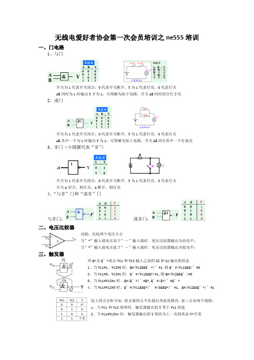
无线电爱好者协会第一次会员培训之ne555培训一、门电路1、与门开关为1代表开关闭合,0代表开关断开。
Y为1代表灯亮,0代表灯灭AB同时为1时输出Y才为1,可理解为如下电路,开关AB同时闭合灯才亮2、或门开关为1代表开关闭合,0代表开关断开。
Y为1代表灯亮,0代表灯灭AB其中一个为1时输出Y为1,可理解为如上电路,开关AB闭合其中一个灯就亮3、非门(小圆圈代表“非”)开关为1代表开关闭合,0代表开关断开。
Y为1代表灯亮,0代表灯灭开关A闭合,则灯灭;A断开,则灯亮4、“与非”门和“或非”门与非门:或非门:二、电压比较器功能:比较两个电压大小当”+”输入端电压高于”-”输入端时,电压比较器输出为高电平;当”+”输入端电压低于”-”输入端时,电压比较器输出为低电平;三、触发器用Q*及Q’*表示Vc1和Vc2输入之前的G2和G1输出的状态1、当Vc1=1,Vc2=0时,Q=(Vc2&&Q’*)’=1,则Q’=(Vc1&&Q)’=02、当Vc1=0,Vc2=1时,Q’=(Vc1&&Q*)=1,则Q=(Vc2&&Q’)=03、当Vc1=Vc2=1时,Q=(Q’*)’=Q*,Q’=(Q*)’=Q’*4、当Vc1=Vc2=0时,Q’=(Vc1&&Q*)’ =(0&&Q*)’=1, Q=(Vc2&&Q’*)’=1综上四点分析可知,除去第四点不在我们考虑范围内,前三点有两个规律:1、当Vc1和Vc2相异时,触发器输出的Y等于Vc1的值2、当Vc1=Vc2=1时,触发器输出的Y保持为上一次的状态Y*不变四、ne555内部结构→图1图3图1可分成3个模块,如图2;为使电路简单化,如图3我们知道触发器输入什么会输出什么后,把触发器直接用方框代替即可,这样就不需要每次都去分析触发器如何工作1、初始分析:(1)如左图,ne555内部有三个5k欧的电阻,三个电阻分别占用电压为1/3 Vcc,则VR1和VR2的电势分别为2/3 Vcc,1/3Vcc,分别接入比较器C1的“+”和C2的“-”,则(a)当Vi1>2/3 Vcc时,Vc1=0;当Vi1<2/3 Vcc时,Vc1=1;(b)当Vi2>1/3 Vcc时,Vc2=1;当Vi2<1/3Vcc时,Vc2=0。
NE555震荡器、计时器IC说明及运用

NE555震盪器、計時器IC說明及運用喬治查爾斯電子電路網http://georgecharles.idv.stNE555 (Timer IC)大約在1971年由Signetics Corporation發佈,在當時是唯一非常快速且商業化的Timer IC,在往後的30年來非常普遍被使用,且延伸出許多的應用電路,儘管近年來CMOS技術版本的Timer IC如MOTOROLA的MC1455已被大量的使用,但原規格的NE555依然正常的在市場上供應,儘管新版IC在功能上有部份的改善,但其腳位勁能並沒變化,所以到目前都可直接的代用。
功能特性:•供應電壓 4.5-18V•供應電流 3-6 mA•輸出電流 225mA (max)•上升/下降時間 100 ns動作:z外部電容決定On-Off輸出脈衝周期的長短。
z充電時間是常電容充電至供應電壓的63.7%時=時間常數, = RC。
模式:z單觸發(單穩)z震盪器(非穩)單觸發(單穩):z當輸入端接收觸發脈衝後產生一個固定長度的脈衝輸出。
z可外加特定的選擇電路改變脈衝輸出的長度。
z也可用在延遲器設計。
z輸出脈衝長度取決於RC。
震盪器(非穩):z產生一連續方波。
z頻率及周期取決於RC的值。
頻率的計算規則:f = 1/(.693 x C x (R1 + 2 x R2))z脈衝的ON周期為t1秒,OFF周期為t2秒,所以t1+t2為全周期。
z t1周期約55 to 95%。
D = t1/t = (R1 + R2) / (R1 + 2R2)t1 = .693(R1+R2)Ct2 = .693 x R2 x C腳位功能:1: 接地Ground ,通常為電源的負電。
2: 觸發Trigger最少要有1u Second 約1/3Vcc正電壓脈衝足以觸發,觸發脈衝是一個短暫的高至低的脈衝,輸出為一負脈衝。
觸發的時間須小於RC的時間常數,如果這個腳位持續保持在低電位,其輸出會一直到高電位,直到觸發輸入回到高電位。
(完整word版)NE555详细介绍和引脚图
NE555 (Timer IC)大约在1971年由Signetics Corporation发布,在当时是唯一非常快速且商业化的Timer IC,在往后的30年来非常普遍被使用,且延伸出许多的应用电路,尽管近年來CMOS技术版本的Timer IC 如MOTOROLA的MC1455已被大量的使用,但原规格的NE555依然正常的在市场上供应,尽管新版IC在功能上有部份的改善,但其脚位劲能并没变化,所以到目前都可直接的代用。
NE555是属于555系列的计时IC的其中的一种型号,555系列IC的接脚功能及运用都是相容的,只是型号不同的因其价格不同其稳定度、省电、可产生的振荡频率也不大相同;而555是一个用途很广且相当普遍的计时IC,只需少数的电阻和电容,便可产生数位电路所需的各种不同频率的脉波讯号。
a。
NE555的特点有:1。
只需简单的电阻器、电容器,即可完成特定的振荡延时作用。
其延时范围极广,可由几微秒至几小时之久。
2。
它的操作电源范围极大,可与TTL,CMOS等逻辑闸配合,也就是它的输出准位及输入触发准位,均能与这些逻辑系列的高、低态组合。
3.其输出端的供给电流大,可直接推动多种自动控制的负载.4。
它的计时精确度高、温度稳定度佳,且价格便宜。
b。
NE555引脚位配置说明下:NE555接脚图ne555的结构图Pin 1 (接地) -地线(或共同接地),通常被连接到电路共同接地。
Pin 2 (触发点)-这个脚位是触发NE555使其启动它的时间周期。
触发信号上缘电压须大于2/3 VCC,下缘须低于1/3 VCC 。
Pin 3 (输出) —当时间周期开始555的输出输出脚位,移至比电源电压少1。
7伏的高电位.周期的结束输出回到O伏左右的低电位。
于高电位时的最大输出电流大约200 mA .Pin 4 (重置)-一个低逻辑电位送至这个脚位时会重置定时器和使输出回到一个低电位。
它通常被接到正电源或忽略不用。
Pin 5 (控制)—这个接脚准许由外部电压改变触发和闸限电压。
NE555中文资料
NE555中文资料通用时基电路NE555P概述:封装外形图NE555P是一块通用时基电路,电路包含24个晶体管,2 Array个二极管和17个电阻,组成阈值比较器,触发比较器,RS触发器,复位输入,放电和输出等6部分。
采用DIP8、SOP8封装形式。
主要特点:关闭时间小于2 S。
最大工作频率大于500kHz。
定时可从微秒级至小时级(由外接电阻电容精确控制)。
可工作于振荡方式或单稳态方式。
输出电流大,200mA(可提供或灌入)。
占空比可调。
可同TTL电路相接。
温度稳定性好,0.005%/℃功能框图极限值(绝对最大额定值,若无其它规定,Tamb=25℃)电特性(若无其它规定,Vcc=5~15V,Tamb=25℃)参考参数注:* 指外部RC回路漂移不计入时间参数。
应用图555芯片引脚图及引脚描述555的8脚是集成电路工作电压输入端,电压为5~18V,以UCC表示;从分压器上看出,上比较器6脚A1的5脚接在R1和R2之间,所以5脚的电压固定在2UCC/3上;下比较器A2接在R2与R3之间,A2的同相输入端电位被固定在UCC/3上。
NE555管脚功能介绍:1脚为地。
2脚为触发输入端;3脚为输出端,输出的电平状态受触发器控制,而触发器受上比较器6脚和下比较器2脚的控制。
当触发器接受上比较器A1从R脚输入的高电平时,触发器被置于复位状态,3脚输出低电平;2脚和6脚是互补的,2脚只对低电平起作用,高电平对它不起作用,即电压小于1Ucc/3,此时3脚输出高电平。
6脚为阈值端,只对高电平起作用,低电平对它不起作用,即输入电压大于2 Ucc/3,称高触发端,3脚输出低电平,但有一个先决条件,即2脚电位必须大于1Ucc/3时才有效。
3脚在高电位接近电源电压Ucc,输出电流最大可打200mA。
4脚是复位端,当4脚电位小于0.4V时,不管2、6脚状态如何,输出端3脚都输出低电平。
5脚是控制端。
7脚称放电端,与3脚输出同步,输出电平一致,但7脚并不输出电流,所以3脚称为实高(或低)、7脚称为虚高。
NE555中文资料详解

NE555中文资料详解555芯片引脚图及引脚描述555的8脚是集成电路工作电压输入端,电压为5~18V,以UCC表示;从分压器上看出,上比较器6脚A1的5脚接在R1和R2之间,所以5脚的电压固定在2UCC/3上;下比较器A2接在R2与R3之间,A2的同相输入端电位被固定在UCC/3上。
NE555管脚功能介绍:1脚为地。
2脚为触发输入端;3脚为输出端,输出的电平状态受触发器控制,而触发器受上比较器6脚和下比较器2脚的控制。
当触发器接受上比较器A1从R脚输入的高电平时,触发器被置于复位状态,3脚输出低电平;2脚和6脚是互补的,2脚只对低电平起作用,高电平对它不起作用,即电压小于1Ucc/3,此时3脚输出高电平。
6脚为阈值端,只对高电平起作用,低电平对它不起作用,即输入电压大于2Ucc/3,称高触发端,3脚输出低电平,但有一个先决条件,即2脚电位必须大于1Ucc/3时才有效。
3脚在高电位接近电源电压Ucc,输出电流最大可打200mA。
4脚是复位端,当4脚电位小于0.4V时,不管2、6脚状态如何,输出端3脚都输出低电平。
5脚是控制端。
7脚称放电端,与3脚输出同步,输出电平一致,但7脚并不输出电流,所以3脚称为实高(或低)、7脚称为虚高。
1555集成电路的框图及工作原理555集成电路开始是作定时器应用的,所以叫做555定时器或555时基电路。
但后来经过开发,它除了作定时延时控制外,还可用于调光、调温、调压、调速等多种控制及计量检测。
此外,还可以组成脉冲振荡、单稳、双稳和脉冲调制电路,用于交流信号源、电源变换、频率变换、脉冲调制等。
由于它工作可靠、使用方便、价格低廉,目前被广泛用于各种电子产品中,555集成电路内部有几十个元器件,有分压器、比较器、基本R-S触发器、放电管以及缓冲器等,电路比较复杂,是模拟电路和数字电路的混合体,如图1所示。
555芯片管脚介绍555集成电路是8脚封装,双列直插型,如图2(A)所示,按输入输出的排列可看成如图2(B)所示。
NE555的介绍及应用
如果要电子爱好者把平时最常见、应用最广泛的集成电路做个排名,那么大名鼎鼎的555时基集成电路肯定是首屈一指的了。
我作为一名业余电子爱好者,不光对分析电路和实际制作有着浓厚的兴趣,对它们的发展历史和围绕着它们引发的故事也同样有着强烈的好奇。
下文是我搜集整理的围绕着555时基集成电路从诞生到现在发生的一系列故事,与大家共赏。
555时基集成电路是一个把模拟电路和数字电路组合而成的混合电路,它将模拟功能与逻辑功能整合在一片独立的集成电路上,极大的拓宽了模拟集成电路的应用范围。
555被广泛用于各种各样的计时器,脉冲发生器和振荡器等场合。
凭借着模数结合的优势,555可以独立构成多种功能电路,且精度非常高,能够产生精确的时间延迟和振荡。
时基集成电路的设计构想是在1970年由Hans R.Camenzind和Jim Ba ll提出的。
设计原型经过测试,被移植到Monochip模拟阵列,由Wayne Foletta和Qualidyne Semicond uctors的工程师们进行具体设计。
事后,Signetics公司接管了他们的设计并开始投入生产,正式量产的第一批555集成电路于1971年面世。
根据应用范围又把555按编号细分为两个级别:商用级的NE555,温度范围0℃~+70℃和军用级的SE555,温度范围-55℃~+125℃。
555时基集成电路的封装分为两种形式:高可靠性的金属罐式8脚封装(T封装)和低成本的环氧塑料8脚双列直插式封装(V封装)。
封装号后缀在元件编号后面,因此Signetics公司生产的555按全编号分别为NE555V、NE555T、SE555V和SE555T。
这些元件编号对于业余应用来说,可以不必太过深究,但是若要把元件用在重要场合,从设计的环节就需要仔细考虑了。
一、555的由来555名称的由来,按照很多技术文章的说法,555时基集成电路的3个“5”,是源自它电路基片上的三个误差极小的5kΩ电阻构成的基准电压电路。
NE555简介
NE555简介555 定时器成本低,性能可靠,只需要外接几个电阻、电容,就可以实现多谐振荡器、单稳态触发器及施密特触发器等脉冲产生与变换电路。
它也常作为定时器广泛应用于仪器仪表、家用电器、电子测量及自动控制等方面。
555定时器的内部电路框图和外引脚排列图分别如图2.9.1 和图 2.9.2 所示。
它内部包括两个电压比较器,三个等值串联电阻,一个RS 触发器,一个放电管T 及功率输出级。
它提供两个基准电压VCC/3 和2VCC /3555 定时器的功能主要由两个比较器决定。
两个比较器的输出电压控制RS 触发器和放电管的状态。
在电源与地之间加上电压,当5 脚悬空时,则电压比较器C1 的同相输入端的电压为2VCC /3,C2 的反相输入端的电压为VCC /3。
若触发输入端TR 的电压小于VCC /3,则比较器C2 的输出为0,可使RS 触发器置1,使输出端OUT=1。
如果阈值输入端TH 的电压大于2VCC/3,同时TR 端的电压大于VCC /3,则C1 的输出为0,C2 的输出为1,可将RS 触发器置0,使输出为0 电平。
它的各个引脚功能如下:1脚:外接电源负端VSS或接地,一般情况下接地。
8脚:外接电源VCC,双极型时基电路VCC的范围是4.5 ~ 16V,CMOS型时基电路VCC的范围为3 ~ 18V。
一般用5V。
3脚:输出端V o2脚:低触发端脚:TH高触发端4脚:是直接清零端。
当此端接低电平,则时基电路不工作,此时不论TR、TH处于何电平,时基电路输出为“0”,该端不用时应接高电平。
5脚:VC为控制电压端。
若此端外接电压,则可改变内部两个比较器的基准电压,当该端不用时,应将该端串入一只0.01μF电容接地,以防引入干扰。
7脚:放电端。
该端与放电管集电极相连,用做定时器时电容的放电。
在1脚接地,5脚未外接电压,两个比较器A1、A2基准电压分别为的情况下,555时基电路的功能表如表6—1示。
表6—1 555定时器的功能表清零端高触发端TH 低触发端Q 放电管T 功能0 导通直接清零××1 0 1 x 保持上一状态保持上一状态1 1 0 1 截止置11 0 0 1 截止置11 1 1 0 导通清零主要用于产生脉冲信号。
NE555参数范文
NE555参数范文NE555是由三片五极管(NPN和PNP)构成的超大规模集成电路,具有16个引脚。
其功能包括一输入放大器、两个比较器、一片RS触发器和一个输出级,能够产生多种定时和脉冲信号。
此外,NE555还具备稳定的输出特性,在较广电压范围内均能正常工作。
NE555的工作原理主要是基于RS触发器和比较器的操作。
通过控制引脚之间的电压关系,可以实现不同的功能。
在正常工作时,NE555以单稳态多谐振荡模式工作,输出的频率和占空比可以由外部元件调节,从而满足不同的应用需求。
1.GND(引脚1):地线,用于提供电路的参考零电压。
2.TRIG(引脚2):外部触发器输入引脚,用于设置NE555开始工作的触发条件。
3.OUT(引脚3):输出引脚,提供经过放大的定时和脉冲信号。
4.RESET(引脚4):复位引脚,用于将NE555重新置为初始状态。
5.CTRLVCC(引脚5):电源引脚,用于供应NE555的工作电源。
6.THRESH(引脚6):比较器阈值输入引脚,用于控制输出引脚的状态变化。
7.DISCH(引脚7):放电引脚,用于提供外部放电通路。
8.VCC(引脚8):正电源引脚,用于提供NE555的工作电源。
1.供电电压范围:NE555的工作电压范围通常为4.5V至16V,可以根据实际需求进行选取。
2.输出电流:NE555的输出电流通常为200mA,这意味着它可以驱动较大负载电流。
3.工作温度范围:NE555的工作温度范围通常为0°C至70°C,可以适应大多数的工作环境。
4.阈值电压:NE555的比较器阈值电压通常为1/3VCC,用于控制输出引脚的状态变化。
5.触发电压:NE555的触发电压通常为2/3VCC,用于设置开始工作的触发条件。
6.存储温度范围:NE555的存储温度范围通常为-65°C至150°C,可以适应大部分的储存环境。
总之,NE555作为一种常用的集成电路,在电子电路中具有广泛的应用。
NE555引脚功能及应用

NE555引脚功能及应用1.VCC引脚:该引脚是NE555的电源引脚,用于接入电源正极。
通常工作电源电压为5V-18V,可以根据具体应用需求进行选择。
2.GND引脚:该引脚是NE555的电源引脚,用于接入电源负极和地。
在使用中,GND引脚与电源的负极和电路的共地连接。
3.TRIG引脚:该引脚是NE555的触发引脚,用于接受来自外部电路的触发信号。
当TRIG引脚接收到低电平信号时,将会触发NE555的工作。
4.THRES引脚:该引脚是NE555的阈值引脚,用于接受来自外部电路的阈值信号。
当THRES引脚接收到高电平信号时,将会触发NE555的工作。
5.CONT引脚:该引脚是NE555的控制引脚,用于接受来自外部电路的控制信号。
通过对该引脚的电压进行调整,可以改变NE555工作的频率。
6.RESET引脚:该引脚是NE555的复位引脚,用于接受来自外部电路的复位信号。
当RESET引脚接收到低电平信号时,将会使NE555回到初始状态。
7.OUT引脚:该引脚是NE555的输出引脚,用于输出NE555的工作信号。
当NE555触发或复位后,OUT引脚会输出相应的高或低电平信号。
8.DIS引脚:该引脚是NE555的放电引脚,用于控制NE555内部电容的放电。
当DIS引脚接收到高电平信号时,内部电容会开始放电;当DIS引脚接收到低电平信号时,内部电容停止放电。
1.脉冲发生器:通过调整TRIG和THRES引脚的电压,可以实现不同频率和占空比的脉冲输出。
可以用于产生钟脉冲、驱动LED的闪烁等应用。
2.电压控制振荡器:通过控制CONT引脚的电压,可以调整NE555的工作频率。
可以作为音乐发生器、声音效果器等的振荡器部分。
3.定时器:将TRIG引脚和THRES引脚通过外部电路连接到一定的阻容元件组合,可以实现精确的定时功能。
可以用于实现定时开关、定时报警器等应用。
4.脉宽调制器:通过控制THRES引脚和DIS引脚的电压,可以实现不同占空比的脉宽调制输出。
ne555dr中文资料
TRIG THRES 1Features3Description These devices are precision timing circuits capable of •Timing From Microseconds to Hours producing accurate time delays or oscillation.In the •Astable or Monostable Operation time-delay or mono-stable mode of operation,the •Adjustable Duty Cycle timed interval is controlled by a single external resistor and capacitor network.In the a-stable mode•TTL-Compatible Output Can Sink or Source of operation,the frequency and duty cycle can beUp to 200mA controlled independently with two external resistors•On Products Compliant to MIL-PRF-38535,and a single external capacitor.All Parameters Are Tested Unless Otherwise The threshold and trigger levels normally are two-Noted.On All Other Products,Production thirds and one-third,respectively,of V CC .TheseProcessing Does Not Necessarily Include levels can be altered by use of the control-voltageTesting of All Parameters.terminal.When the trigger input falls below the triggerlevel,the flip-flop is set,and the output goes high.If2Applications the trigger input is above the trigger level and the•Fingerprint Biometrics threshold input is above the threshold level,the flip-flop is reset and the output is low.The reset (RESET)•Iris Biometrics input can override all other inputs and can be used to•RFID Readerinitiate a new timing cycle.When RESET goes low,the flip-flop is reset,and the output goes low.Whenthe output is low,a low-impedance path is providedbetween discharge (DISCH)and ground.The output circuit is capable of sinking or sourcingcurrent up to 200mA.Operation is specified forsupplies of 5V to 15V.With a 5-V supply,outputlevels are compatible with TTLinputs.Device Information (1)PART NUMBER PACKAGEBODY SIZE (NOM)PDIP (8)9.81mm ×6.35mm SOP (8)6.20mm ×5.30mm xx555TSSOP (8)3.00mm ×4.40mm SOIC (8) 4.90mm ×3.91mm (1)For all available packages,see the orderable addendum atthe end of the datasheet.4Simplified Schematic找电子元器件上宇航军工NA555,NE555,SA555,SE555SLFS022I–SEPTEMBER1973–REVISED SEPTEMBER2014Table of Contents8.1Overview (9)1Features (1)8.2Functional Block Diagram (9)2Applications (1)8.3Feature Description (9)3Description (1)8.4Device Functional Modes (12)4Simplified Schematic (1)9Applications and Implementation (13)5Revision History (2)9.1Application Information (13)6Pin Configuration and Functions (3)9.2Typical Applications (13)7Specifications (4)10Power Supply Recommendations (18)7.1Absolute Maximum Ratings (4)11Device and Documentation Support (19)7.2Handling Ratings (4)11.1Related Links (19)7.3Recommended Operating Conditions (4)11.2Trademarks (19)7.4Electrical Characteristics (5)11.3Electrostatic Discharge Caution (19)7.5Operating Characteristics (6)11.4Glossary (19)7.6Typical Characteristics (7)12Mechanical,Packaging,and Orderable 8Detailed Description (9)Information (19)5Revision HistoryChanges from Revision H(June2010)to Revision I Page •Updated document to new TI enhanced data sheet format (1)•Deleted Ordering Information table (1)•Added Military Disclaimer to Features list (1)•Added Applications (1)•Added Device Information table (1)•Moved T stg to Handling Ratings table (4)•Added DISCH switch on-state voltage parameter (5)•Added Device and Documentation Support section (19)•Added ESD warning (19)•Added Mechanical,Packaging,and Orderable Information section (19)2Submit Documentation Feedback Copyright©1973–2014,Texas Instruments IncorporatedProduct Folder Links:NA555NE555SA555SE555IMPORTANT NOTICE AND DISCLAIMERTI PROVIDES TECHNICAL AND RELIABILITY DATA(INCLUDING DATASHEETS),DESIGN RESOURCES(INCLUDING REFERENCE DESIGNS),APPLICATION OR OTHER DESIGN ADVICE,WEB TOOLS,SAFETY INFORMATION,AND OTHER RESOURCES“AS IS”AND WITH ALL FAULTS,AND DISCLAIMS ALL WARRANTIES,EXPRESS AND IMPLIED,INCLUDING WITHOUT LIMITATION ANY IMPLIED WARRANTIES OF MERCHANTABILITY,FITNESS FOR A PARTICULAR PURPOSE OR NON-INFRINGEMENT OF THIRD PARTY INTELLECTUAL PROPERTY RIGHTS.These resources are intended for skilled developers designing with TI products.You are solely responsible for(1)selecting the appropriate TI products for your application,(2)designing,validating and testing your application,and(3)ensuring your application meets applicable standards,and any other safety,security,or other requirements.These resources are subject to change without notice.TI grants you permission to use these resources only for development of an application that uses the TI products described in the resource.Other reproduction and display of these resources is prohibited.No license is granted to any other TI intellectual property right or to any third party intellectual property right.TI disclaims responsibility for,and you will fully indemnify TI and its representatives against,any claims, damages,costs,losses,and liabilities arising out of your use of these resources.TI’s products are provided subject to TI’s Terms of Sale(/)or other applicable terms available either on ti or provided in conjunction with such TI products.TI’s provision of these resources does not expand or otherwise alter TI’s applicable warranties or warranty disclaimers for TI products.Mailing Address:Texas Instruments,Post Office Box655303,Dallas,Texas75265Copyright© 2020,Texas Instruments Incorporated。
NE555芯片原理

NE555芯片(1)简介NE555 是属于555 系列的计时IC(IC 即集成电路)的其中的一种型号,是一种用途很广且相当普遍的计时IC,利用它再外接电阻电容可以极其方便地搭建出单稳态触发器和多谐振荡器,被广泛应用在波形的产生与变换、测量与控制、家用电器、电子玩具等领域。
(2)外观(3)参数功能特性A、供电电压:4.5V—18VB、供应电流:3-6 mAC、输出电流:225mA (max)D、上升/下降时间:100 ns(4)内部结构(等效逻辑结构)(5)NE555 各引脚介绍Pin 1 (接地) -地线(或共同接地) ,通常被连接到电路共同接地。
Pin 2 (触发点) -这个脚位是触发NE555使其启动它的时间周期。
触发信号如果要高电平,须大于2/3 VCC,低电平须低于1/3 VCC。
Pin 3 (输出) -当芯片开始工作时555 的输出脚位。
于高电位时的最大输出电流大约200 mA 。
U=0)送至这个脚位时会复位整个芯片,使芯片重 Pin 4 (复位) –一个低逻辑电位(41新开始工作(字母上有横杠表示低电平有效)。
Pin 5 (控制) -这个接脚准许由外部电压改变触发和闸限电压。
当计时器经营在稳定或振荡的运作方式下,这输入能用来改变或调整输出频率。
Pin 6 (重置锁定) - 重置锁定并使输出呈低态。
当这个接脚的电压从1/3 VCC电压以下移至2/3 VCC 以上时启动这个动作。
Pin 7 (放电) -这个接脚和主要的输出接脚3 有相同的电流输出能力,当输出为ON 时为LOW,对地为高阻抗,当输出为OFF 时为HIGH,对地为低阻抗。
Pin 8 (V cc) -这是555 个计时器IC 的正电源电压端。
供应电压的范围是+4.5 伏特(最小值)至+16 伏特(最大值)。
(6)真值表。
- 1、下载文档前请自行甄别文档内容的完整性,平台不提供额外的编辑、内容补充、找答案等附加服务。
- 2、"仅部分预览"的文档,不可在线预览部分如存在完整性等问题,可反馈申请退款(可完整预览的文档不适用该条件!)。
- 3、如文档侵犯您的权益,请联系客服反馈,我们会尽快为您处理(人工客服工作时间:9:00-18:30)。
TRIG THRES 1Features3Description These devices are precision timing circuits capable of •Timing From Microseconds to Hours producing accurate time delays or oscillation.In the •Astable or Monostable Operation time-delay or mono-stable mode of operation,the •Adjustable Duty Cycle timed interval is controlled by a single external resistor and capacitor network.In the a-stable mode•TTL-Compatible Output Can Sink or Source of operation,the frequency and duty cycle can beUp to 200mA controlled independently with two external resistors•On Products Compliant to MIL-PRF-38535,and a single external capacitor.All Parameters Are Tested Unless Otherwise The threshold and trigger levels normally are two-Noted.On All Other Products,Production thirds and one-third,respectively,of V CC .TheseProcessing Does Not Necessarily Include levels can be altered by use of the control-voltageTesting of All Parameters.terminal.When the trigger input falls below the triggerlevel,the flip-flop is set,and the output goes high.If2Applications the trigger input is above the trigger level and the•Fingerprint Biometrics threshold input is above the threshold level,the flip-flop is reset and the output is low.The reset (RESET)•Iris Biometrics input can override all other inputs and can be used to•RFID Readerinitiate a new timing cycle.When RESET goes low,the flip-flop is reset,and the output goes low.Whenthe output is low,a low-impedance path is providedbetween discharge (DISCH)and ground.The output circuit is capable of sinking or sourcingcurrent up to 200mA.Operation is specified forsupplies of 5V to 15V.With a 5-V supply,outputlevels are compatible with TTLinputs.Device Information (1)PART NUMBER PACKAGEBODY SIZE (NOM)PDIP (8)9.81mm ×6.35mm SOP (8)6.20mm ×5.30mm xx555TSSOP (8)3.00mm ×4.40mm SOIC (8) 4.90mm ×3.91mm (1)For all available packages,see the orderable addendum atthe end of the datasheet.4Simplified Schematic找电子元器件上宇航军工NA555,NE555,SA555,SE555SLFS022I–SEPTEMBER1973–REVISED SEPTEMBER2014Table of Contents8.1Overview (9)1Features (1)8.2Functional Block Diagram (9)2Applications (1)8.3Feature Description (9)3Description (1)8.4Device Functional Modes (12)4Simplified Schematic (1)9Applications and Implementation (13)5Revision History (2)9.1Application Information (13)6Pin Configuration and Functions (3)9.2Typical Applications (13)7Specifications (4)10Power Supply Recommendations (18)7.1Absolute Maximum Ratings (4)11Device and Documentation Support (19)7.2Handling Ratings (4)11.1Related Links (19)7.3Recommended Operating Conditions (4)11.2Trademarks (19)7.4Electrical Characteristics (5)11.3Electrostatic Discharge Caution (19)7.5Operating Characteristics (6)11.4Glossary (19)7.6Typical Characteristics (7)12Mechanical,Packaging,and Orderable 8Detailed Description (9)Information (19)5Revision HistoryChanges from Revision H(June2010)to Revision I Page •Updated document to new TI enhanced data sheet format (1)•Deleted Ordering Information table (1)•Added Military Disclaimer to Features list (1)•Added Applications (1)•Added Device Information table (1)•Moved T stg to Handling Ratings table (4)•Added DISCH switch on-state voltage parameter (5)•Added Device and Documentation Support section (19)•Added ESD warning (19)•Added Mechanical,Packaging,and Orderable Information section (19)2Submit Documentation Feedback Copyright©1973–2014,Texas Instruments IncorporatedProduct Folder Links:NA555NE555SA555SE555IMPORTANT NOTICE AND DISCLAIMERTI PROVIDES TECHNICAL AND RELIABILITY DATA(INCLUDING DATASHEETS),DESIGN RESOURCES(INCLUDING REFERENCE DESIGNS),APPLICATION OR OTHER DESIGN ADVICE,WEB TOOLS,SAFETY INFORMATION,AND OTHER RESOURCES“AS IS”AND WITH ALL FAULTS,AND DISCLAIMS ALL WARRANTIES,EXPRESS AND IMPLIED,INCLUDING WITHOUT LIMITATION ANY IMPLIED WARRANTIES OF MERCHANTABILITY,FITNESS FOR A PARTICULAR PURPOSE OR NON-INFRINGEMENT OF THIRD PARTY INTELLECTUAL PROPERTY RIGHTS.These resources are intended for skilled developers designing with TI products.You are solely responsible for(1)selecting the appropriate TI products for your application,(2)designing,validating and testing your application,and(3)ensuring your application meets applicable standards,and any other safety,security,or other requirements.These resources are subject to change without notice.TI grants you permission to use these resources only for development of an application that uses the TI products described in the resource.Other reproduction and display of these resources is prohibited.No license is granted to any other TI intellectual property right or to any third party intellectual property right.TI disclaims responsibility for,and you will fully indemnify TI and its representatives against,any claims, damages,costs,losses,and liabilities arising out of your use of these resources.TI’s products are provided subject to TI’s Terms of Sale(/)or other applicable terms available either on ti or provided in conjunction with such TI products.TI’s provision of these resources does not expand or otherwise alter TI’s applicable warranties or warranty disclaimers for TI products.Mailing Address:Texas Instruments,Post Office Box655303,Dallas,Texas75265Copyright© 2020,Texas Instruments Incorporated。