CY7C1051DV33芯片手册
CY7C025资料
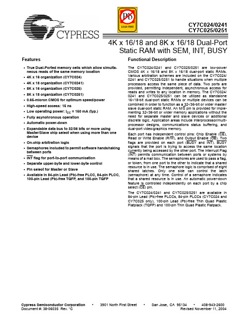
Notes: 1. BUSY is an output in master mode and an input in slave mode. 2. I/O0 –I/O8 on the CY7C0241/0251. 3. I/O9 –I/O17 on the CY7C0241/0251. 4. A12L on the CY7C025/0251. 5. A12R on the CY7C025/0251.
CY7C024/0241 CY7C025/0251
Logic Block DiagramL L源自R/W R UBRL
LBR CE R OE R
OE L
[3] I/O 8L – I/O 15L
I/O 0L – I/O 7L
[2] [1]
I/O CONTROL
I/O CONTROL
I/O8R – I/O15R[3] I/O 0R– I/O 7R [2]
Document #: 38-06035 Rev. *C
Page 2 of 21
元器件交易网
CY7C024/0241 CY7C025/0251
Pin Configurations (continued)
OEL VCC R/WL SEML CEL UBL LBL NC [4] A11L A10L
INTERRUPT SEMAPHORE ARBITRATION
CE R OE R UB R LB R R/W R SEM R
M/S
INTR
Pin Configurations
84-Pin PLCC Top View
SEM L CEL UB L GND I/O 1L I/O 0L OE L V CC LB L NC [4] A11L R/WL I/O 7L I/O 6L I/O 5L I/O 4L I/O 3L I/O 2L A 10L A A 8L A7L A6L A5L A4L A3L A2L A1L A0L INTL BUSYL GND M/S BUSYR INTR A0R A1R A2R A3R A4R A5R A6R
CTM1051(A)MG超小体积高速CAN隔离收发器说明书
输入特性参数 符号 条件 最小值 典型值 最大值 单位输入电压V CCCTM1051AMG 3.15 3.3 3.45 VDC CTM1051MG4.75 55.25 TXD 逻辑电平 高电平 V IH 0.7V CC -- V CC +0.5 低电平 V IL 0 -- 0.3V CC RXD 逻辑电平高电平 V OH I RXD =-1.5mA V CC -0.4 V CC -0.2 -- 低电平V OL I RXD =1.5mA-- 0.2 0.4 TXD 驱动电流 I T 2 -- -- mA RXD 输出电流 I R -- -- 10 TXD 上拉电阻 R TXD--10--kΩ 串行接口CTM1051AMG 3.3V 标准CAN 控制器接口 CTM1051MG5V 标准CAN 控制器接口产品特性—————————————————◆符合ISO 11898-2标准 ◆未上电节点不影响总线 ◆单网络最多可连接110个节点 ◆超小体积,仅为一般产品的40% ◆外壳及灌封材料符合UL94 V-0标准 ◆具有极低电磁辐射和高的抗电磁干扰性 ◆高低温特性好,满足工业级产品要求CTM1051(A)MG产品数据手册超小体积高速CAN 隔离收发器产品系列————————————————产品型号 温度范围 隔离耐压 封装 CTM1051AMG -40℃~+105℃ 2500VDC DIP8 CTM1051MG-40℃~+105℃2500VDCDIP8产品应用————————————————◆仪器、仪表 ◆石油化工 ◆电力监控 ◆工业控制 ◆轨道交通 ◆汽车电子 ◆智能家居等Data Sheet产品型号———————————————————————————————————————产品型号电源电压 (电压范围) (VDC) 静态电流 (mA,Typ)最大工作电流(mA)传输波特率 (bps) 节点数 (pcs)类型CTM1051AMG 3.3 (3.15-3.45) 8 120 40k~1M110高速CTM1051MG5(4.75-5.25)99040k~1M输出特性参数符号条件最小值典型值最大值单位显性电平(逻辑0)CANH V(OD)CANH R L=60Ω 2.75 3.5 4.5VDC CANL V(OD)CANL R L=60Ω 0.5 1.5 2.25 隐性电平(逻辑1)CANH V(OR)CANH no load 2 2.5 3CANL V(OR)CANL no load 2 2.5 3 差分电平显性(逻辑0) V diff(d)R L=60Ω 1.5 2 3隐性(逻辑1) V diff(r)no load -0.05 0 0.05 总线引脚最大耐压V X CANH、CANL -40 -- +40总线引脚漏电流I LV CC=0VV CANH/L=5V-5 -- +5 µA CAN总线接口符合ISO 11898-2 标准,双绞线输出传输特性参数名称符号条件最小值典型值最大值单位数据延时TXD发送延时t T R L=60Ω -- 60 --ns RXD接收延时t R R L=60Ω -- 80 --循环延迟t PD(TXD-RXD)R L=60Ω -- 140 210 TXD显性超时时间t to(dom)TXD V TXD=0V 0.3 -- 3.8 ms极限特性参数条件最小值典型值最大值单位输入冲击电压(1)(1s,max)CTM1051AMG -0.7 -- 5VDCCTM1051MG -0.7 -- 7 引脚焊接温度焊点距离外壳1.5mm,10秒-- -- 300 ℃热插拔不支持一般特性参数条件最小值典型值最大值单位隔离电压输入-输出,时间1分钟,漏电流小于1mA2500 -- -- VDC 绝缘电阻输入-输出,绝缘电压500VDC 1 -- -- GΩ封装尺寸12.80×10.20×7.70 mm外壳材料黑色阻燃塑胶外壳,符合UL94 V-0标准环境特性参数名称条件最小值典型值最大值单位工作温度-40 -- +105℃存储温度-55 -- +125外壳温升Ta=25℃-- 15 25存储湿度无凝结-- -- 95 %冷却方式自然空冷EMC特性EMS静电放电抗扰度IEC/EN 61000-4-2 Contact ±4kV (裸机,总线端口) (2)Perf. Criteria B脉冲群抗扰度IEC/EN 61000-4-4 ±2kV(裸机,总线端口) (2)Perf. Criteria B浪涌抗扰度IEC/EN 61000-4-5 共模±2kV(裸机,总线端口) (2)Perf. Criteria BIEC/EN 61000-4-5 差模±2kV,共模±4kV(应用电路图3、图4)(3)Perf. Criteria B 传导骚扰抗扰度IEC/EN 61000-4-6 3Vr.m.s(裸机) Perf. Criteria A注:(1)输入电压不能超过所规定范围值,否则可能会造成永久性不可恢复的损坏。
柯拉尔(Carrier)33CS-33PS年型 PremierLink retrofit 控制器说明

Copyright 2007 Carrier CorporationForm 33CS-33PSThe PremierLink retrofit controllers offer:•continuous monitoring and regulation of the rooftop unit•compatibility with Carrier diagnostic display tools•other devices can read and write data to the controller•ability to connect unit to the Carrier Comfort Network® (CCN) systemFeatures/BenefitsThe PremierLink retrofit rooftop controller is an intelligent control thatcontinuously monitors and regulates rooftop operation with reliability and precision that minimizes downtime to ensure maximum occupant comfort.The PremierLink controller is compati-ble with the Carrier ComfortNetwork (CCN) system. Carrier’s diag-nostic standard tier display tools such as System Pilot™ or Touch Pilot™ device can be used with the PremierLink con-troller. User interfaces include the CCN Service Tool, ComfortVIEW™ and ComfortWORKS ® software.When the PremierLink controller is used as part of the CCN system, otherdevices such as the CCN data transfer, 3V™ linkage coordinator, or Comfort Controller can read data from or write data to the retrofit controller.PREMIERLINK™Retrofit RooftopController33CSPREMLKProductSpecificationa33-91472Extensive control capabilitiesThe 33CSPREMLK retrofit controller provides the following features and benefits:•provides software clock and local occupancy schedule for local occu-pancy control (requires time broad-caster and hardware clock from another device in the system)•uses remote timeclock input to pro-vide occupancy control through exter-nal contacts or this input can be reconfigured for use with a door or window switch to disable heating and cooling if a door or window is left open•provides continous or intermittent fan operation in the occupied mode•features supply air temperature limit-ing and integrated safeties for DX (direct expansion), gas, electric and heat pump units•provides field tests that enables the user to check output points and verify their functionality•controls two stages of DX cooling to maintain space temperature set point •ability to provide occupied and unoc-cupied dehumidification•controls up to 3 stages of gas heat or combination of mechanical and elec-tric heat to maintain space tempera-ture set point•ability to control exhaust fan based on economizer or occupancy on 2-stage heat units•ability to control reversing valve on heat pump units•provides temperature compensated start of heating or cooling to achieve set point by the start of the sched- uled occupied time•provides alarms for analog tempera-ture input(s) out of range•provides alarm for space tempera-ture deviation from desired set point •adjustable filter maintenance timer •allows manual and system overrides of selected input/output channels•supports CCN remote timed override, set point adjustment and manual fan control override•provides Broadcast Acknowledger capability for CCN (configuration)•conforms to the general require- ments for CCN devices•modulates control of economizer to assist mechanical cooling without adversely affecting compressor performance•provides ventilation monitoring with optional CO 2 ventilation sensor •compatible with T55 space sensor and T56 space sensor with set point adjustment, timed override and ser-vice port jack•compatibility with T58 communicat-ing sensor provides set point adjust-ment, timed override, force fan, and read equipment mode•compatibility with System Pilot as a communicating sensor providing set point adjustment, timed override, and a user interface for programming, configuration, and monitoring and forcing points•support a local or global occupancy schedule or remote start input status to determine occupancy•individual fan start delay for each Premierlink™ board upon occupancy change.Available for wide range of rooftop applicationsThe PremierLink controller is available as a field retrofit application and can control one or several rooftop units with (multiple controllers) from 3 to 25 tons. In addition, it has an integrated economizer controller that eliminates the need for a separate cir-cuit board.The PremierLink controller can be installed on the following Carrier rooftop units: 48/50HE (2 to 5 tons), 50HEQ (2 to 5 tons), 48/50HJ (3 to 25 tons),50HJQ (3 to 15 tons), 48TF/50TFF (3 to 121/2 tons), 50TFQ (3 to 10 tons), 48/50TJ (121/2 to 25 tons), and 48/50TM (3 to 25 tons). Other Carrier equipment and non-Carrier equipment can also be controlled by PremierLink controller. Con-tact a Carrier Factory Sales representative for more information.Flexibility for every applicationThe PremierLink controller is an ad- vanced microprocessor-based control. PremierLink is precision controlled to send heating and cooling only when needed, reducing energy use and operat-ing costs.Carrier linkage compatibilityWhen used as the air source for a 3V™ zoning system, the PremierLink control-ler will use occupancy schedules, zone temperature, and set points from the 3V linkage coordinator. The PremierLink controller provides the 3V linkage coordi-nator with the unit’s operating mode and supply-air temperature to provide coordi-nation of the individual member zone's local mode with the system mode.Additional control featuresThe PremierLink controller provides addi-tional control features such as Occupied/Unoccupied schedulinginitialized via the network. The Premier-Link controller offers override invoked from a wall sensor during unoccupied hours from 1 to 4 hours in 1-hour increments.The PremierLink controller offers venti-lation monitoring with an optional CO 2 ventilation sensor. The CO 2 ventilation sensor measures the amount of ventilation needed by the space and a proportional integral derivative loop (PID) calculation makes adjustments to the economizer minimum position during occupied opera-tion. The indoor CO 2 will be compared to an outdoor CO 2 reference before making adjustments to the economizer minimum position.Using a space sensor with set point adjustment, timed override and service port jack, the PremierLink controller will provide intelligent compressor staging and economizer operation.Modulating control of the economizer will assist mechanical cooling without adversely affecting compressor perfor-mance. Economizer assisted cooling is determined from a comparison of space temperature, outside air temperature and an enthalpy switch input. The switch input can also be used for differential enthalpy input, meeting ASHRAE (American Soci-ety of Heating, Refrigeration, and Air Conditioning Engineers) Standard 90.1. The T58 Communicating Space tem-perature sensor with service port jack pro-vides set point adjustment, timed override, force fan and read equipment mode and measures and maintains room tempera-ture by communicating with the Premier-Link controller.Using an optional indoor humidity sensor, the PremierLink control can providedehumidification control on units that are equipped to provide dehumidification.Simple mounting and ease of installationThe PremierLink controller has an inte-grated plastic cover with secured with two plastic tabs that can be removed for ease of installation.For ease of installation, the PremierLink controller is provided with removable Molex connectors which include pigtails for easy installation to unit or sensors using spade connectors or wire nuts. The removable connectors are designed so that they can be inserted one way so as to prevent installation errors. The Premier-Link controller also provides an RJ-11 modular phone jack for the Network Ser-vice Tool connection to the module via the Carrier Comfort Network® (CCN) communications.Features/Benefits (cont)3User interfaceThe PremierLink™ controller is designed to allow a service person or building owner to configure and operate the unit through the CCN user interface. A user interface is not required for day-to-day operation. All maintenance, config-uration, setup, and diagnostic information is available through the L evel II communications port to allow data access by an attached computer running Network Service Tool, ComfortVIEW ™, or ComfortWORKS ® software.Data access also can be obtained from System Pilot™ or Touch Pilot™ devices.Wiring connectionsField wiring is 18 to 22 AWG (American Wire Gage). The PremierLink controller is a NEC (National Electrical Code)Class 2 rated device.Inputs•space temperature sensor •set point adjustment•outdoor air temperature sensor •indoor air quality sensor•outdoor air quality sensor/indoor humidity sensor •compressor lockout •fire shutdown •supply fan status•remote time clock/door switch •enthalpy status Outputs•economizer •fan•cool stage 1•cool stage 2•heat stage 1•heat stage 2•heat stage 3/exhaust/reversing valve/dehumidify/occupiedPower supply2-wire, 24 VAC ± 15% at 40 va, 60 HzPower consumptionNormal operating supply range is 18 to 32 VAC with mini-mum consumption of 10 VAHardware (memory)Internal flash memory of 64KSpecified sensing temperature rangeThe PremierL ink controller space temperature range is –40 to 245 F (–40 to 118 C). The PremierLink controller has an allowable control set point range from 40 to 90 F(4 to 32 C) for heating and 45 to 99 F (7 to 37 C) for cooling.CommunicationsThe number of PremierLink controllers is limited only by the maximum number of controllers allowed on a CCN sys-tem. Bus length may not exceed 4000 ft (1219 m), with no more than 60 devices on any 1000 ft (305 m) section.Optically isolated RS-485 repeaters are required every 1000 ft (305 m). Status and control data is transmitted at a baud rate of between 9600 and 38.4K.Activity indicatorsTwo activity indicators present on the PremierLink control-ler indicate activity. A green LED will indicate activity on the communication port and a red LED will indicate status of processor operation.DimensionsHeight: 53/4-in. (146 mm)Width: 81/2-in. (216 mm)Depth: 3-in. (76 mm)Minimum service dimensionsHeight: 7-in. (178 mm)Width: 9-in. (229 mm)Depth: 4-in. (102 mm)Environmental ratingsOperating Temperature: –40 to 158 F (–40 to 70 C) at 10to 95% RH (non-condensing)Storage Temperature: –40 to 185 F (–40 to 85 C) at 10 to 95% RH (non-condensing)VibrationPerformance vibration: all planes/directions, 1.5G at 20to 300 HzShockOperation: all planes/directions, 5G peak, 11 ms Storage: all planes/directions, 100G peak, 11 msCorrosionOffice environment. Indoor use only.ApprovalsL isted under UL 873, UL 94-V0/5VB (plastic), and UL ,Canada.Standard complianceCE Mark, ASHRAE 90 and ASHRAE 62-99 compliant.NOTE: Compliance standards subject to change without notice.Field-installed accessoriesSupply air temperature sensor — The 33ZCSENSAT supply air temperature sensor is required for all applica-tions to monitor the temperature of the air delivered. A second supply air temperature sensor set to thermostat mode (or a space temperature sensor) must be installed in the return air for proper economizer and IAQ (indoor air quality) control.Space temperature sensor with override button —The space temperature sensor monitors room temperature which is used by the PremierLink controller to determine the temperature of conditioned air that is allowed into the space.SpecificationsManufacturer reserves the right to discontinue, or change at any time, specifications or designs without notice and without incurring obligations.New Pg 4Catalog No. 04-52330009-01Printed in U.S.A. Form 33CS-33PSReplaces: 33CS-19PS Book 14Tab 11a 13aCarrier Corporation • Syracuse, New Y ork 132216-07Book 1Tab 1CS1a33-9142The 33ZCT55SPT (T55) space temperature sensor with override button is required for all applications. The space temperature sensor monitors room temperature which is used by the PremierLink™ controller to deter-mine the temperature of conditioned air that is allowed into the space.Space te mperature sensor with override button and se t point adjustme nt — The 33ZCT56SPT (T56) space temperature sensor with override button and set point adjustment can be used in place of the 33ZCT55SPT (T55) space temperature sensor if local set point adjustment is required. The space temperature sensor monitors room temperature which is used by the PremierLink controller to determine the temperature of conditioned air that is allowed into the space.T58 communicating sensor with override button,set point adjustment, and manual fan control —The 33ZCT58SPT (T58) communicating room sensor with override button, set point adjustment, and manual fan control can be used in place of the 33ZCT55SPT space temperature sensor. The T58 communicating room sensor measures and maintains room temperature by communicating with the controller.Syste m Pilot™ (33PILOT-01) — The System Pilot device is a communicating room sensor with override button and set point adjustment that can be used in place of the T56 space temperature sensor. The System Pilot communicating room sensor measures and main-tains room temperature by communicating with the controller.The System Pilot device can be also be used to install,commission, and monitor a PremierL ink controller, a 3V™ zoning system, a universal controller, and all other devices operating on the CCN system. The System Pilot device has a hardware clock and can be used as CCN time broadcaster.Humidity se nsor — The relative humidity sensor (33ZCSENSRH-01) is required for dehumidification control. The rooftoop unit must be equiped with neces-sary accesories to perfom dehumidification. The sensor can also be used for monitoring only.NOTE: The relative humidity sensor and outdoor CO 2sensor cannot be installed on the same zone controller.CO 2 sensor — Three different CO 2 sensors are avail-able for monitoring space indoor-air quality.The 33ZCSENCO2 sensor is an indoor, wall-mount-ed sensor with an L ED (light-emitting diode) display.The sensor has an analog output (0 to 10 vdc or 4 to 20mA) over a range of 0 to 2000 ppm. An SPDT contact is provided to close at 1000 ppm with a hysteresis of 50 ppm.The 33ZCT55CO2 sensor is an indoor, wall-mounted sensor without display. The CO 2 sensor also includes a space temperature sensor with override button.The 33ZCT56CO2 sensor is an indoor, wall-mounted sensor without display. The CO 2 sensor also includes a space temperature sensor with override button and tem-perature offset.DimensionsField-installed accessories (cont)。
USB控制芯片cy7c68013中文手册

■ 3.3V 工作电压,容限输入为 5V
■ 向量化 USB 中断和 GPIF/FIFO 中断
■ 16 K 字节片上代码/数据 RAM
■ 四个可编程的 BULK/INTERRUPT/ISOCHRONOUS 端点 ❐ 缓冲区大小选项:两倍,三倍,四倍
■ 附加的可编程 (BULK/INTERRUPT) 64 位端点
■ 8 位或 16 位外部数据接口
■ 可生成智能介质标准错误校正码 ECC
■ 通用可编程接口 (General Programmable Interface, GPIF) ❐ 可与大多数并行接口直接连接 ❐ 由可编程波形描述符和配置寄存器定义波形 ❐ 支持多个 Ready (RDY) 输入和 Control (CTL) 输出
4 KB8/16源自FIFO丰富的 I/O 接口包含 两个 USART
通用可编程 I/F 符合 ASIC/DSP 或 总线标准,例如 ATAPI、 EPP 等
高达 96 MB/s 突发速率
增强型 USB 核 简化 8051 代码
“软配置”容易 进行固件更换
FIFO 和端点存储器 (主控端或从属端操作)
1.1 特色 (仅限 CY7C68013A/14A)
片上 PLL 可根据收发器 /PHY 的需要将 24 MHz 振荡器倍频到 480 MHz,而内部计数器可将其分频以用作 8051 时钟。默认的 8051 时钟频率是 12 MHz。 8051 的时钟频率可以由 8051 通过 CPUCS 寄存器动态更改。
USB控制芯片cy7c68013中文手册
■ CY7C68013A:适合非电池供电应用 ❐ 挂起电流:300 μA (typ)
■ 有五种无铅封装供选择,可包含多达 40 个 GPIO ❐ 128 引脚 TQFP (40 个 GPIO)、 100 引脚 TQFP (40 个 GPIO)、 56 引脚 QFN (24 个 GPIO)、 56 引脚 SSOP (24 个 GPIO)和 56 引脚 VFBGA (24 个 GPIO)
注 1. 以 115 KBaud 的速率运行也是可能的,只要分别针对 UART0、 UART1 或针对二者将 8051 SMOD0 或 SMOD1 位编程为 “1” 即可。
文件编号:001-50431 修订版 **
第 3 页,共 61 页
[+] Feedback
CY7C68013A, CY7C68014A CY7C68015A, CY7C68016A
■ 有商业和工业温度等级供选择 (除 VFBGA 外的所有封装)
Cypress Semiconductor Corporation • 198 Champion Court 文件编号:001-50431 修订版 **
• San Jose, CA 95134-1709 • 408-943-2600
修订时间 2008 年 12 月 11 日
1.2 特色 (仅限 CY7C68015A/16A)
■ CY7C68016A:适合电池供电应用 ❐ 挂起电流:100 μA (typ)
■ CY7C68015A:适合非电池供电应用 ❐ 挂起电流:300 μA (typ)
■ 采用无铅 56 引脚 QFN 封装 (26 个 GPIO) ❐ 比 CY7C68013A/14A 多 2 个 GPIO,可在同样的空间内实现 额外的功能
CY7C1411AV18资料

Errata Revision: *CMay 02, 2007RAM9 QDR-I/DDR-I/QDR-II/DDR- II ErrataCY7C129*DV18/CY7C130*DV25CY7C130*BV18/CY7C130*BV25/CY7C132*BV25CY7C131*BV18 / CY7C132*BV18/CY7C139*BV18CY7C191*BV18/CY7C141*AV18 / CY7C142*AV18/CY7C151*V18 /CY7C152*V18This document describes the DOFF issue for QDRII/DDRII and the Output Buffer and JTAG issues for QDRI/DDRI/QDRII/DDRII. Details include trigger conditions, possible workarounds and silicon revision applicability.This document should be used to compare to the respective datasheet for the devices to fully describe the device functionality.Please contact your local Cypress Sales Representative for availability of the fixed devices and any other questions.Devices AffectedTable 1. List of Affected devicesProduct StatusAll of the above densities and revisions are available in sample as well as production quantities.QDR/DDR DOFF Pin, Output Buffer and JTAG Issues Errata SummaryThe following table defines the issues and the fix status for the different devices which are affected.Density & Revision Part Numbers Architecture 9Mb - Ram9(90 nm)CY7C130*DV25QDRI/DDRI 9Mb - Ram9(90 nm)CY7C129*DV18QDRII 18Mb - Ram9(90nm)CY7C130*BV18CY7C130*BV25CY7C132*BV25QDRI/DDRI18Mb - Ram9(90nm)CY7C131*BV18CY7C132*BV18CY7C139*BV18CY7C191*BV18QDRII/DDRII36Mb - Ram9(90nm)CY7C141*AV18CY7C142*AV18QDRII/DDRII 72Mb -Ram9(90nm)CY7C151*V18CY7C152*V18QDRII/DDRIIItemIssueDeviceFix Status1.DOFF pin is used for enabling/dis-abling the DLL circuitry within the SRAM. To enable the DLL circuitry, DOFF pin must be externally tied HIGH. The QDR-II/DDR-II devices have an internal pull down resistor of ~5K . The value of the external pull-up resistor should be 500 or less in order to ensure DLL is enabled.9Mb - “D” Rev - Ram918Mb - “B” Rev - Ram936Mb - “A” Rev - Ram972Mb - Ram9QDR-II/DDR-II DevicesThe fix involved removing the in-ternal pull-down resistor on the DOFF pin. The fix has been im-plemented on the new revision and is now available.ΩΩTable 2.Issue Definition and fix status for different devices1. DOFF Pin Issue•ISSUE DEFINITIONThis issue involves the DLL not turning ON properly if a large resistor is used (eg:-10K ) as an external pullup resistor to enable the DLL. If a 10K or higher pullup resistor is used externally, the voltage on DOFF is not high enough to enable the DLL.•PARAMETERS AFFECTEDThe functionality of the device will be affected because of the DLL is not turning ON properly. When the DLL is enabled, all AC and DC parameters on the datasheet are met. •TRIGGER CONDITION(S)Having a 10K or higher external pullup resistor for disabling the DOFF pin.•SCOPE OF IMPACTThis issue will alter the normal functionality of the QDRII/DDRII devices when the DLL is disabled.•EXPLANATION OF ISSUEFigure 1 shows the DOFF pin circuit with an internal 5K internal resistor. The fix planned is to disable the internal 5K leaker.•WORKAROUND2.O/P Buffer enters a locked up unde-fined state after controls or clocks are left floating. No proper read/write access can be done on the device until a dummy read is performed.9Mb - “D” Rev - Ram918Mb - “B” Rev - Ram936Mb - “A” Rev - Ram972Mb - Ram9QDR-I/DDR-I/QDR-II/DDR-II Devices The fix has been implemented onthe new revision and is now avail-able.3.The EXTEST function in the JTAG test fails when input K clock is floating in the JTAG mode.9Mb - “D” Rev - Ram918Mb - “B” Rev - Ram936Mb - “A” Rev - Ram972Mb - Ram9QDR-I/DDR-I/QDR-II/DDR-II DevicesThe fix involved bypassing the ZQ circuitry in JTAG mode. This was done by overriding the ZQ circuit-ry by the JTAG signal. The fix has been implemented on the new re-vision and is now available.Figure 1.DOFF pin with the 5K internal resistorItemIssueDeviceFix StatusΩΩΩΩΩΩThe workaround is to have a low value of external pullup resistor for the DOFF pin (recommended value is <500). When DOFF pins from multiple QDR devices are connected through the same pull-up resistors on the board, it is recommended that this DOFF pin be directly connected to Vdd due to the lower effective resistance since the "leakers" are in parallel.Figure 2 shows the proposed workaround and the fix planned.•FIXSTATUSFix involved removing the internal pull-down resistor on the DOFF pin. The fix has been implemented on the new revision and is now available. The new revision is an increment of the existing revision. The following table lists the devices affected, current revision and the new revision after the fix.Table 3.List of Affected Devices and the new revison2.Output Buffer IssueFigure 2.Proposed workaround with the 500 external pullupCurrent Revision New Revision after the FixCY7C129*DV18CY7C129*EV18CY7C131*BV18CY7C131*CV18CY7C132*BV18CY7C132*CV18CY7C139*BV18CY7C139*CV18CY7C191*BV18CY7C191*CV18CY7C141*AV18CY7C141*BV18CY7C142*AV18CY7C142*BV18CY7C151*V18CY7C151*AV18CY7C152*V18CY7C152*AV18ΩΩ•ISSUE DEFINITIONThis issue involves the output buffer entering an unidentified state when the input signals (only Control signals or Clocks) are floating during reset or initialization of the memory controller after power up. •PARAMETERS AFFECTEDNo timing parameters are affected. The device may drive the outputs even though the read operation is not enabled. A dummy read is performed to clear this condition.•TRIGGER CONDITION(S)Input signals(namely RPS# for QDR-I/QDRII , WE# and LD# for DDR-I/DDRII) or Clocks (K/K# and/or C/C#) are floating during reset or initialization of the memory controller after power up.•SCOPE OF IMPACTThis issue will jeopardize any number of writes or reads which take place after the controls or clock are left floating. This can occur anywhere in the SRAM access ( all the way from power up of the memory device to transitions taking place for read/write accesses to the memory device) if the above trigger conditions are met.•EXPLANATION OF ISSUEFigure 3 shows the output register Reset circuit with an SR Latch circled. This latch has two inputs with one of them coming from some logic affected by the clock and RPS#(QDR) or WE# and LD#(DDR).The issue happens when clocks are glitching/toggling with controls floating. This will cause the SR latch to be taken into an unidentified state. The SR Latch will need to be reset by a dummy read operation if this happens. Array•WORKAROUNDThis is viable only if the customer has the trigger conditions met during reset or initialization of the memory controller after power up. In order for the workaround to perform properly, Cypress recommends the insertion of a minimum of 16 “dummy” READ operations to every SRAM device on the board prior to writing any meaningful data into the SRAM. After this one “dummy” READ operation, the device will perform properly.“Dummy” READ is defined as a read operation to the device that is not meant to retrieve required data. The “dummy” READ can be to any address location in the SRAM. Refer to Figure 4 for the dummy read implemen-tation.In systems where multiple SRAMs with multiple RPS# lines are used, a dummy read operation will have to be performed on every SRAM on the board. Below is an example sequence of events that can be performed before valid access can be performed on the SRAM.1) Initialize the Memory Controller2) Assert RPS# Low for each of the memory devicesNote:For all devices with x9 bus configuration, the following sequence needs to be performed:1) For the 72M / 36M / 18M x9 devices drive address pin A2 / A10 / A3 low respectively and perform dummyread.2) For the 72M / 36M / 18M x9 devices drive address pin A2 / A10 / A3 high respectively and perform dummyread.If the customer has the trigger conditions met during normal access to the memory then there is no workaround at this point.•FIX STATUSThe fix has been implemented on the new revision and is now available. The new revision is an increment of the existing revision. Please refer to Table 4 for the list of devices affected, current revision and the new revision after the fix.3. JTAG Mode Issue•ISSUE DEFINITIONIf the input clock (K Clock) is left floating when the device is in JTAG mode, spurious high frequency noise on this input can be interpreted by the device as valid clocks. This could cause the impedance matching circuitry (ZQ) on the QDR/DDR devices to periodically load itself with incorrect values. These incorrect values in the ZQ register could force the outputs into a High-Impedance state. The ZQ circuitry requires at least 1000 valid K clock cycles to drive the outputs from high impedance to low impedance levels.•PARAMETERS AFFECTEDThis issue only affects the EXTEST command when the device is in the JTAG mode. The normal functionality of the device will not be affected.•TRIGGER CONDITION(S)EXTEST command executed immediately after power-up without providing any K clock cycles.•SCOPE OF IMPACTThis issue only impacts the EXTEST command when device is tested in the JTAG mode. Normal functionality of the device is not affected. •EXPLANATION OF ISSUEImpedance matching circuitry (ZQ) is present on the QDR/DDR devices to set the desired impedance on the outputs. This ZQ circuitry is updated every 1000 clock cycles of K clock to ensure that the impedance of the O/P is set to valid state. However, when the device is operated in the JTAG mode immediately after power-up, high frequency noise on the input K clock can be treated by the ZQ circuitry as valid clocks thereby setting the outputs in to a high-impedance mode. If a minimum of 1000 valid K clocks are applied before performing the JTAG test, this should clear the ZQ circuitry and ensure that the outputs are driven to valid impedance levels.•WORKAROUNDElimination of the issue: After power-up, before any valid operations are performed on the device, insert a minimum of 1000 valid clocks on K input.•FIX STATUSThe fix involved bypassing the ZQ circuitry in JTAG mode. This was done by overriding the ZQ circuitry by the JTAG signal. The fix has been implemented on the new revision and is now available. The new revision is an increment of the existing revision. Please refer to Table 4 for the list of devices affected, current revision and the new revision after the fix..Table 4.List of Affected devices and the new revisionCurrent Revision New Revision after the FixCY7C129*DV18CY7C129*EV18CY7C130*DV25CY7C130*EV25CY7C130*BV18CY7C130*CV18CY7C130*BV25CY7C130*CV25CY7C132*BV25CY7C132*CV25CY7C131*BV18CY7C131*CV18CY7C132*BV18CY7C132*CV18CY7C139*BV18CY7C139*CV18CY7C191*BV18CY7C191*CV18CY7C141*AV18CY7C141*BV18CY7C142*AV18CY7C142*BV18CY7C151*V18CY7C151*AV18CY7C152*V18CY7C152*AV18ReferencesAll 90nm QDRI/DDRI/QDRII/DDRII datasheets:-Table 5.List of Datasheet spec# for the Affected devicesSpec#Part#DensityArchitecture38-05628CY7C1304DV259-MBIT QDR(TM) SRAM 4-WORD BURST 38-05632CY7C1308DV259-MBIT DDR-I SRAM 4-WORD BURST 001-00350CY7C1292DV18/1294DV189-MBIT QDR- II(TM) SRAM 2-WORD BURST 38-05621CY7C1316BV18/1916BV18/1318BV18/1320BV1818-MBIT DDR-II SRAM 2-WORD BURST 38-05622CY7C1317BV18/1917BV18/1319BV18/1321BV1818-MBIT DDR-II SRAM 4-WORD BURST 38-05623CY7C1392BV18/1393BV18/1394BV1818-MBIT DDR-II SIO SRAM 2-WORD BURST 38-05631CY7C1323BV2518-MBIT DDR-I SRAM 4-WORD BURST 38-05630CY7C1305BV25/1307BV2518-MBIT QDR(TM) SRAM 4-WORD BURST 38-05627CY7C1303BV25/1306BV2518-MBIT QDR(TM) SRAM 2-WORD BURST 38-05629CY7C1305BV18/1307BV1818-MBIT QDR(TM) SRAM 4-WORD BURST 38-05626CY7C1303BV18/1306BV1818-MBIT QDR(TM) SRAM 2-WORD BURST 38-05619CY7C1310BV18/1910BV18/1312BV18/1314BV1818-MBIT QDR - II (TM) SRAM 2-WORD BURST 38-05620CY7C1311BV18/1911BV18/1313BV18/1315BV1818-MBIT QDR - II SRAM 4-WORD BURST 38-05615CY7C1410AV18/1425AV18/1412AV18/1414AV1836-MBIT QDR-II(TM) SRAM 2-WORD BURST 38-05614CY7C1411AV18/1426AV18/1413AV18/1415AV1836-MBIT QDR(TM)-II SRAM 4-WORD BURST 38-05616CY7C1416AV18/1427AV18/1418AV18/1420AV1836-MBIT DDR-II SRAM 2-WORD BURST 38-05618CY7C1417AV18/1428AV18/1419AV18/1421AV1836-MBIT DDR-II SRAM 4-WORD BURST 38-05617CY7C1422AV18/1429AV18/1423AV18/1424AV1836-MBIT DDR-II SIO SRAM 2-WORD BURST 38-05489CY7C1510V18/1525V18/1512V18/1514V1872-MBIT QDR-II SRAM 2-WORD BURST 38-05363CY7C1511V18/1526V18/1513V18/1515V1872-MBIT QDR(TM)-II SRAM 4-WORD BURST 38-05563CY7C1516V18/1527V18/1518V18/1520V1872-MBIT DDR-II SRAM 2-WORD BURST 38-05565CY7C1517V18/1528V18/1519V18/1521V1872-MBIT DDR-II SRAM 4-WORD BURST 38-05564CY7C1522V18/1529V18/1523V18/1524V1872-MBITDDR-II SIO SRAM 2-WORD BURSTDocument History PageDocument Title: RAM9 QDR-I/DDR-I/QDR-II/DDR- II Errata Document #: 001-06217 Rev. *CREV.ECN NO.IssueDateOrig. ofChange Description of Change**419849See ECN REF New errata for Ram9 QDR2/DDR2 SRAMs.*A493936See ECN QKS Added Output buffer and JTAG mode issues, Item#2 and #3Added 9Mb QDR-II Burst of 2 and QDR-1/DDR-I part numbers.*B733176See ECN NJY Added missing part numbers in the title for Spec#’s 38-05615,38-05614,38-05363,38-05563 on Table 5 on page 7.*C1030020 See ECN TBE Updated the fix status of the three issues, and modified the description forthe Output Buffer workaround for x9 devices on page 5.。
cy7c68001

CY7C68001 CY7C68001EZ-USB SX2™High-Speed USB Interface DeviceTABLE OF CONTENTS1.0 EZ-USB SX2™ FEATURES (7)1.1 Introduction (7)1.2 Features (7)1.3 Block Diagram (7)2.0 APPLICATIONS (8)2.1 System Diagram (8)3.0 FUNCTIONAL OVERVIEW (9)3.1 USB Signaling Speed (9)3.2 Buses (9)3.3 Boot Methods (9)3.3.1 EEPROM Organization (9)3.3.2 Default Enumeration (10)3.4 Interrupt System (10)3.4.1 Architecture (10)3.4.2 ITENABLE Register Bit Definition (10)3.5 Resets and Wakeup (11)3.5.1 Reset (11)3.5.2 USB Reset (11)3.5.3 Wakeup (11)3.6 Endpoint RAM (11)3.6.1 Size (11)3.6.2 Organization (11)3.6.3 Endpoint Configurations (High-speed Mode) (12)3.6.4 Default Endpoint Memory Configuration (12)3.7 External Interface (12)3.7.1 Architecture (12)3.7.2 Control Signals (13)3.7.3 IFCLK (13)3.7.4 FIFO Access (13)3.7.5 FIFO Flag Pins Configuration (14)3.7.6 Default FIFO Programmable Flag Set-up (14)3.7.7 FIFO Programmable Flag (PF) Set-up (14)3.7.8 Command Protocol (14)4.0 ENUMERATION (15)4.1 Standard Enumeration (15)4.2 Default Enumeration (16)5.0 ENDPOINT 0 (16)6.0 PIN ASSIGNMENTS (17)6.1 56-pin SSOP (17)6.2 56-pin QFN (18)6.3 CY7C68001 Pin Descriptions (19)7.0 REGISTER SUMMARY (21)7.1 IFCONFIG Register 0x01 (22)7.1.1 Bit 7: IFCLKSRC (22)7.1.2 Bit 6: 3048MHZ (22)7.1.3 Bit 5: IFCLKOE (22)TABLE OF CONTENTS (continued)7.1.4 Bit 4: IFCLKPOL (22)7.1.5 Bit 3: ASYNC (22)7.1.6 Bit 2: STANDBY (22)7.1.7 Bit 1: FLAGD/CS# (22)7.1.8 Bit 0: DISCON (22)7.2 FLAGSAB/FLAGSCD Registers 0x02/0x03 (22)7.3 POLAR Register 0x04 (23)7.3.1 Bit 7: WUPOL (23)7.3.2 Bit 5: PKTEND (23)7.3.3 Bit 4: SLOE (24)7.3.4 Bit 3: SLRD (24)7.3.5 SLWR Bit 2 (24)7.3.6 EF Bit 1 (24)7.3.7 FF Bit 0 (24)7.4 REVID Register 0x05 (24)7.5 EPxCFG Register 0x06–0x09 (24)7.5.1 Bit 7: VALID (24)7.5.2 Bit 6: DIR (24)7.5.3 Bit [5,4]: TYPE1, TYPE0 (24)7.5.4 Bit 3: SIZE (25)7.5.5 Bit 2: STALL (25)7.5.6 Bit [1,0]: BUF1, BUF0 (25)7.6 EPxPKTLENH/L Registers 0x0A–0x11 (25)7.6.1 Bit 7: INFM1 EPxPKTLENH.7 (26)7.6.2 Bit 6: OEP1 EPxPKTLENH.6 (26)7.6.3 Bit 5: ZEROLEN EPxPKTLENH.5 (26)7.6.4 Bit 4: WORDWIDE EPxPKTLENH.4 (26)7.6.5 Bit [2..0]: PL[X:0] Packet Length Bits (26)7.7 EPxPFH/L Registers 0x12–0x19 (26)7.7.1 DECIS EPxPFH.7 (26)7.7.2 PKSTAT EPxPFH.6 (26)7.7.3 IN:PKTS(2:0)/OUT:PFC[12:10] EPxPFH[5:3] (27)7.8 EPxISOINPKTS Registers 0x1A–0x1D (27)7.9 EPxxFLAGS Registers 0x1E–0x1F (27)7.9.1 EPxPF Bit 6, Bit 2 (28)7.9.2 EPxEF Bit 5, Bit 1 (28)7.9.3 EPxFF Bit 4, Bit 0 (28)7.10 INPKTEND/FLUSH Register 0x20 (28)7.11 USBFRAMEH/L Registers 0x2A, 0x2B (28)7.12 MICROFRAME Registers 0x2C (29)7.13 FNADDR Register 0x2D (29)7.14 INTENABLE Register 0x2E (29)7.14.1 SETUP Bit 7 (29)7.14.2 EP0BUF Bit 6 (29)7.14.3 FLAGS Bit 5 (29)7.14.4 ENUMOK Bit 2 (29)7.14.5 BUSACTIVITY Bit 1 (29)7.14.6 READY Bit 0 (29)TABLE OF CONTENTS (continued)7.15 DESC Register 0x30 (30)7.16 EP0BUF Register 0x31 (30)7.17 SETUP Register 0x32 (30)7.18 EP0BC Register 0x33 (30)8.0 ABSOLUTE MAXIMUM RATINGS (31)9.0 OPERATING CONDITIONS (31)10.0 DC ELECTRICAL CHARACTERISTICS (31)11.0 AC ELECTRICAL CHARACTERISTICS (32)11.1 USB Transceiver (32)11.2 Command Interface (32)11.2.1 Command Synchronous Read (32)11.2.2 Command Synchronous Write (33)11.2.3 Command Asynchronous Read (34)11.2.4 Command Asynchronous Write (34)11.3 FIFO Interface (35)11.3.1 Slave FIFO Synchronous Read (35)11.3.2 Slave FIFO Synchronous Write (36)11.3.3 Slave FIFO Synchronous Packet End Strobe (37)11.3.4 Slave FIFO Synchronous Address (37)11.3.5 Slave FIFO Asynchronous Read (38)11.3.6 Slave FIFO Asynchronous Write (38)11.3.7 Slave FIFO Asynchronous Packet End Strobe (39)11.3.8 Slave FIFO Asynchronous Address (39)11.4 Slave FIFO Address to Flags/Data (39)11.5 Slave FIFO Output Enable (40)11.6 Sequence Diagram (40)11.6.1 Single and Burst Synchronous Read Example (40)11.6.2 Single and Burst Synchronous Write (41)11.6.3 Sequence Diagram of a Single and Burst Asynchronous Read (42)11.6.4 Sequence Diagram of a Single and Burst Asynchronous Write (43)12.0 DEFAULT DESCRIPTOR (44)13.0 GENERAL PCB LAYOUT GUIDELINES (47)14.0 QUAD FLAT PACKAGE NO LEADS (QFN) PACKAGE DESIGN NOTES (47)15.0 ORDERING INFORMATION (48)16.0 PACKAGE DIAGRAMS (48)16.1 56-pin SSOP Package (48)16.2 56-pin QFN Package (49)17.0 DOCUMENT REVISION HISTORY (50)LIST OF FIGURESFIGURE 1-1. BLOCK DIAGRAM (7)FIGURE 2-1. EXAMPLE USB SYSTEM DIAGRAM (8)FIGURE 3-1. ENDPOINT CONFIGURATION (12)FIGURE 6-1. CY7C68001 56-PIN SSOP PIN ASSIGNMENT (17)FIGURE 6-2. CY7C68001 56-PIN QFN ASSIGNMENT (18)FIGURE 11-1. COMMAND SYNCHRONOUS READ TIMING DIAGRAM (32)FIGURE 11-2. COMMAND SYNCHRONOUS WRITE TIMING DIAGRAM (33)FIGURE 11-3. COMMAND ASYNCHRONOUS READ TIMING DIAGRAM (34)FIGURE 11-4. COMMAND ASYNCHRONOUS WRITE TIMING DIAGRAM (34)FIGURE 11-5. SLAVE FIFO SYNCHRONOUS READ TIMING DIAGRAM (35)FIGURE 11-6. SLAVE FIFO SYNCHRONOUS WRITE TIMING DIAGRAM (36)FIGURE 11-7. SLAVE FIFO SYNCHRONOUS PACKET END STROBE TIMING DIAGRAM (37)FIGURE 11-8. SLAVE FIFO SYNCHRONOUS ADDRESS TIMING DIAGRAM (37)FIGURE 11-9. SLAVE FIFO ASYNCHRONOUS READ TIMING DIAGRAM (38)FIGURE 11-10. SLAVE FIFO ASYNCHRONOUS WRITE TIMING DIAGRAM (38)FIGURE 11-11. SLAVE FIFO ASYNCHRONOUS PACKET END STROBE TIMING DIAGRAM (39)FIGURE 11-12. SLAVE FIFO ASYNCHRONOUS ADDRESS TIMING DIAGRAM (39)FIGURE 11-13. SLAVE FIFO ADDRESS TO FLAGS/DATA TIMING DIAGRAM (39)FIGURE 11-14. SLAVE FIFO OUTPUT ENABLE TIMING DIAGRAM (40)FIGURE 11-15. SLAVE FIFO SYNCHRONOUS READ SEQUENCE AND TIMING DIAGRAM (40)FIGURE 11-16. SLAVE FIFO SYNCHRONOUS SEQUENCE OF EVENTS DIAGRAM (40)FIGURE 11-17. SLAVE FIFO SYNCHRONOUS WRITE SEQUENCE AND TIMING DIAGRAM (41)FIGURE 11-18. SLAVE FIFO ASYNCHRONOUS READ SEQUENCE AND TIMING DIAGRAM (42)FIGURE 11-19. SLAVE FIFO ASYNCHRONOUS READ SEQUENCE OF EVENTS DIAGRAM (42)FIGURE 11-20. SLAVE FIFO ASYNCHRONOUS WRITE SEQUENCE AND TIMING DIAGRAM (43)FIGURE 14-1. CROSSSECTION OF THE AREA UNDERNEATH THE QFN PACKAGE (47)FIGURE 14-2. (A) PLOT OF THE SOLDER MASK (WHITE AREA) (47)FIGURE 14-2. (B) X-RAY IMAGE OF THE ASSEMBLY (47)FIGURE 16-1. 56-LEAD SHRUNK SMALL OUTLINE PACKAGE (48)FIGURE 16-2. LF56A 56-PIN QFN PACKAGE (49)LIST OF TABLESTABLE 3-1. DESCRIPTOR LENGTH SET TO 0X06: DEFAULT ENUMERATION (9)TABLE 3-2. DESCRIPTOR LENGTH NOT SET TO 0X06 (9)TABLE 3-3. FIFO ADDRESS LINES SETTING (13)TABLE 3-4. COMMAND ADDRESS BYTE (14)TABLE 3-5. COMMAND DATA BYTE ONE (14)TABLE 3-6. COMMAND DATA BYTE TWO (14)TABLE 3-7. COMMAND ADDRESS WRITE BYTE (15)TABLE 3-8. COMMAND DATA WRITE BYTE ONE (15)TABLE 3-9. COMMAND DATA WRITE BYTE TWO (15)TABLE 3-10. COMMAND ADDRESS READ BYTE (15)TABLE 6-1. SX2 PIN DESCRIPTIONS (19)TABLE 7-1. SX2 REGISTER SUMMARY (21)TABLE 7-2. FIFO FLAG 4-BIT CODING (23)TABLE 7-3. ENDPOINT TYPE (25)TABLE 7-4. ENDPOINT BUFFERING (25)TABLE 7-5. PKTS BITS (27)TABLE 7-6. EPXISOINPKTS (27)TABLE 10-1. DC CHARACTERISTICS (31)TABLE 11-1. COMMAND SYNCHRONOUS READ PARAMETERSWITH INTERNALLY SOURCED IFCLK (32)TABLE 11-2. COMMAND SYNCHRONOUS READ WITH EXTERNALLY SOURCED IFCLK (32)TABLE 11-3. COMMAND SYNCHRONOUS WRITE PARAMETERSWITH INTERNALLY SOURCED IFCLK (33)TABLE 11-4. COMMAND SYNCHRONOUS WRITE PARAMETERSWITH EXTERNALLY SOURCED IFCLK (33)TABLE 11-5. COMMAND READ PARAMETERS (34)TABLE 11-6. COMMAND WRITE PARAMETERS (34)TABLE 11-7. SLAVE FIFO SYNCHRONOUS READ WITH INTERNALLY SOURCED IFCLK (35)TABLE 11-8. SLAVE FIFO SYNCHRONOUS READ WITH EXTERNALLY SOURCED IFCLK (35)TABLE 11-9. SLAVE FIFO SYNCHRONOUS WRITE PARAMETERSWITH INTERNALLY SOURCED IFCLK (36)TABLE 11-10. SLAVE FIFO SYNCHRONOUS WRITE PARAMETERSWITH EXTERNALLY SOURCED IFCLK (36)TABLE 11-11. SLAVE FIFO SYNCHRONOUS PACKET END STROBE PARAMETERS, INTERNALLY SOURCED IFCLK (37)TABLE 11-12. SLAVE FIFO SYNCHRONOUS PACKET END STROBE PARAMETERS, EXTERNALLY SOURCED IFCLK (37)TABLE 11-13. SLAVE FIFO SYNCHRONOUS ADDRESS PARAMETERS (37)TABLE 11-14. SLAVE FIFO ASYNCHRONOUS READ PARAMETERS (38)TABLE 11-15. SLAVE FIFO ASYNCHRONOUS WRITE PARAMETERSWITH INTERNALLY SOURCED IFCLK (38)TABLE 11-16. SLAVE FIFO ASYNCHRONOUS PACKET END STROBE PARAMETERS (39)TABLE 11-17. SLAVE FIFO ASYNCHRONOUS ADDRESS PARAMETERS (39)TABLE 11-18. SLAVE FIFO ADDRESS TO FLAGS/DATA PARAMETERS (39)TABLE 11-19. SLAVE FIFO OUTPUT ENABLE PARAMETERS (40)TABLE 15-1. ORDERING INFORMATION (48)1.0 EZ-USB SX2™ Features1.1IntroductionThe EZ-USB SX2 USB interface device is designed to work with any external master, such as standard micropro-cessors, DSPs, ASICs, and FPGAs to enable USB 2.0 support for any peripheral design. SX2 has a built-in USB trans-ceiver and Serial Interface Engine (SIE), along with a command decoder for sending and receiving USB data. The controller has four endpoints that share a 4-KB FIFO space for maximum flexibility and throughput, as well as Control Endpoint 0. SX2 has three address pins and a selectable 8- or 16- bit data bus for command and data input or output.1.2Features•USB 2.0-certified compliant•Operates at high (480 Mbps) or full (12 Mbps) speed•Supports Control Endpoint 0:—Used for handling USB device requests•Supports four configurable endpoints that share a 4-KB FIFO space—Endpoints 2, 4, 6, 8 for application-specific control and data•Standard 8- or 16-bit external master interface—Glueless interface to most standard microprocessors DSPs, ASICs, and FPGAs—Synchronous or Asynchronous interface•Integrated phase-locked loop (PLL)•3.3V operation, 5V tolerant I/Os•56-pin SSOP and QFN package•Complies with most device class specifications1.3Block Diagram2.0 Applications•DSL modems•ATA interface•Memory card readers•Legacy conversion devices•Cameras•Scanners•Home PNA•Wireless LAN•MP3 players•Networking•PrintersThe “Reference Designs” section of the Cypress web site provides additional tools for typical USB applications. Each reference design comes complete with firmware source code and object code, schematics, and documentation. Please see the Cypress web site at .2.1System DiagramFigure 2-1. Example USB System Diagram3.0Functional Overview 3.1USB Signaling SpeedSX2 operates at two of the three rates defined in the Universal Serial Bus Specification Revision 2.0, dated April 27, 2000:•Full-speed, with a signaling bit rate of 12 Mbits/s•High-speed, with a signaling bit rate of 480 Mbits/s.SX2 does not support the low-speed signaling rate of 1.5 Mbits/s.3.2BusesSX2 features:•A selectable 8- or 16-bit bidirectional data bus•An address bus for selecting the FIFO or Command Interface.3.3Boot MethodsDuring the power-up sequence, internal logic of the SX2 checks for the presence of an I 2C-compatible EEPROM.[1,2] If it finds an EEPROM, it will boot off the EEPROM. When the presence of an EEPROM is detected, the SX2 checks the value of first byte.If the first byte is found to be a 0xC4, the SX2 loads the next two bytes into the IFCONFIG and POLAR registers, respectively. If the fourth byte is also 0xC4, the SX2 enumerates using the descriptor in the EEPROM, then signals to the external master when enumeration is complete via an ENUMOK interrupt (Section 3.4). If no EEPROM is detected, the SX2 relies on the external master for the descriptors. Once this descriptor information is receive from the external master, the SX2 will connect to the USB bus and enumerate.3.3.1EEPROM OrganizationThe valid sequence of bytes in the EEPROM are displayed below.•0xC4: This initial byte tells the SX2 that this is a valid EEPROM with configuration information.•IFCONFIG : This byte contains the settings for the IFCONFIG register. The IFCONFIG register bits are defined in Section 7.1. If the external master requires an interface configuration different from the default, that interface can be specified in this byte.•POLAR : This byte contains the polarities of the interface signals. The POLAR register bits are defined in Section 7.3. If the external master requires signal polarities different from the default, those polarities can be specified in this byte.•Descriptor : This next byte determines whether or not the SX2 loads the descriptor from the EEPROM. If this byte = 0xC4, the SX2 will load the descriptor starting with the next byte. If this byte does not equal 0xC4, the SX2 will wait for descriptor information from the external master.Notes:1.Because there is no direct way to detect which EEPROM type (single or double address) is connected, SX2 uses the EEPROM address pins A2, A1, and A0 to determine whether to send out one or two bytes of address. Single-byte address EEPROMs (24LC01, etc.) should be strapped to address 000 and double-byte EEPROMs (24LC64, etc.) should be strapped to address 001.2.The SCL and SDA pins must be pulled up for this detection method to work properly, even if an EEPROM is not connected. Typical pull-up values are 2.2K –10K Ohms.Table 3-1. Descriptor Length Set to 0x06: Default EnumerationTable 3-2. Descriptor Length Not Set to 0x06Byte Index Description Byte Index Description0xC400xC41IFCONFIG 1IFCONFIG 2POLAR 2POLAR 30xC430xC44Descriptor Length (LSB):0x064Descriptor Length (LSB)5Descriptor Length (MSB): 0x005Descriptor Length (MSB 6VID (LSB)6Descriptor[0]7VID (MSB)7Descriptor[1]8PID (LSB)8Descriptor[2]9PID (MSB) (10)DID (LSB)......11DID (MSB)......•Descriptor Length: The next two bytes indicate the length of the descriptor contained in the EEPROM. The length is loaded least significant byte (LSB) first, then most significant byte (MSB).•Byte 7 Starts Descriptor Information: The descriptor can be a maximum of 500 bytes.3.3.2Default EnumerationAn optional default descriptor can be used to simplify enumeration. Only the Vendor ID (VID), Product ID (PID), and Device ID (DID) need to be loaded by the SX2 for it to enumerate with this default set-up. This information is either loaded from an EEPROM in the case when the presence of an EEPROM (Table3-1) is detected, or the external master may simply load a VID, PID, and DID when no EEPROM is present. In this default enumeration, the SX2 uses the in-built default descriptor (refer to Section 12.0). If the descriptor length loaded from the EEPROM is 6, SX2 will load a VID, PID, and DID from the EEPROM and enumerate. The VID, PID, and DID are loaded LSB, then MSB. For example, if the VID, PID, and DID are 0x0547, 0x1002, and 0x0001, respec-tively, then the bytes should be stored as:•0x47, 0x05, 0x02, 0x10, 0x01, 0x00.If there is no EEPROM, SX2 will wait for the external master to provide the descriptor information. To use the default descriptor, the external master must write to the appropriate register (0x30) with descriptor length equal to 6 followed by the VID, PID, and DID. Refer to Section 4.2 for further information on how the external master may load the values.The default descriptor enumerates four endpoints as listed in the following page:•Endpoint 2: Bulk out, 512 bytes in high-speed mode, 64 bytes in full-speed mode•Endpoint 4: Bulk out, 512 bytes in high-speed mode, 64 bytes in full-speed mode•Endpoint 6: Bulk in, 512 bytes in high-speed mode, 64 bytes in full-speed mode•Endpoint 8: Bulk in, 512 bytes in high-speed mode, 64 bytes in full-speed mode.The entire default descriptor is listed in Section 12.0 of this data sheet.3.4Interrupt System3.4.1ArchitectureThe SX2 provides an output signal that indicates to the external master that the SX2 has an interrupt condition, or that the data from a register read request is available. The SX2 has six interrupt sources: SETUP, EP0BUF, FLAGS, ENUMOK, BUSACTIVITY, and READY. Each interrupt can be enabled or disabled by setting or clearing the corresponding bit in the INTENABLE register. When an interrupt occurs, the INT# pin will be asserted, and the corresponding bit will be set in the Interrupt Status Byte. The external master reads the Interrupt Status Byte by strobing SLRD/SLOE. This presents the Interrupt Status Byte on the lower portion of the data bus (FD[7:0]). Reading the Interrupt Status Byte automatically clears the interrupt. Only one interrupt request will occur at a time; the SX2 buffers multiple pending interrupts.If the external master has initiated a register read request, the SX2 will buffer interrupts until the external master has read the data. This insures that after a read sequence has begun, the next interrupt that is received from the SX2 will indicate that the corresponding data is available. Following is a description of this ITENABLE register.3.4.2ITENABLE Register Bit DefinitionBit 7: SETUPIf this interrupt is enabled, and the SX2 receives a set-up packet from the USB host, the SX2 asserts the INT# pin and sets bit 7 in the Interrupt Status Byte. This interrupt only occurs if the set-up request is not one that the SX2 automatically handles. For complete details on how to handle the SETUP interrupt, refer to Section 5.0 of this data sheet.Bit 6: EP0BUFIf this interrupt is enabled, and the Endpoint 0 buffer becomes available to the external master for read or write operations, the SX2 asserts the INT# pin and sets bit 6 in the Interrupt Status Byte. This interrupt is used for handling the data phase of a set-up request. For complete details on how to handle the EP0BUF interrupt, refer to Section 5.0 of this data sheet.Bit 5: FLAGSIf this interrupt is enabled, and any OUT endpoint FIFO’s state changes from empty to not-empty, the SX2 asserts the INT# pin and sets bit 5 in the Interrupt Status Byte. This is an alternate way to monitor the status of OUT endpoint FIFOs instead of using the FLAGA-FLAGD pins, and can be used to indicate when an OUT packet has been received from the host.Bit 4: ENUMOKIf this interrupt is enabled and the SX2 receives a SET_CONFIGURATION request from the USB host, the SX2 asserts the INT# pin and sets bit 2 in the Interrupt Status Byte. This event signals the completion of the SX2 enumeration process.Bit 1: BUSACTIVITYIf this interrupt is enabled, and the SX2 detects either an absence or resumption of activity on the USB bus, the SX2 asserts the INT# pin and sets bit 1 in the Interrupt Status Byte. This usually indicates that the USB host is either suspending or resuming or that a self-powered device has been plugged in or unplugged. If the SX2 is bus-powered, the external master must put the SX2 into a low-power mode after detecting a USB suspend condition to be USB-compliant.Bit 0: READYIf this interrupt is enabled, bit 0 in the Interrupt Status Byte is set when the SX2 has powered up and performed a self-test. The external master should always wait for this interrupt before trying to read or write to the SX2, unless an external EEPROM with a valid descriptor is present. If an external EEPROM with a valid descriptor is present, the ENUMOK interrupt will occur instead of the READY interrupt after power up. A READY interrupt will also occur if the SX2 is awakened from a low-power mode via the WAKEUP pin. This READY interrupt indicates that the SX2 is ready for commands or data.3.5Resets and Wakeup3.5.1ResetAn input pin (RESET#) resets the chip. The internal PLL stabilizes approximately 7.6 ms after V CC has reached 3.3V. Typically, an external RC network (R = 100 K Ohms, C = 0.1 uf) is used to provide the RESET# signal.3.5.2USB ResetWhen the SX2 detects a USB Reset condition on the USB bus, SX2 handles it like any other enumeration sequence. This means that SX2 will enumerate again and assert the ENUMOK interrupt to let the external master know that it has enumerated. The external master will then be responsible for configuring the SX2 for the application. The external master should also check whether SX2 enumerated at High or Full speed in order to adjust the EPxPKTLENH/L register values accordingly. The last initialization task is for the external master to flush all of the SX2 FIFOs.3.5.3WakeupThe SX2 exits its low-power state when one of the following events occur:•USB bus signals a resume. The SX2 will assert a BUSACTIVITY interrupt.•The external master asserts the WAKEUP pin. The SX2 will assert a READY interrupt.3.6Endpoint RAM3.6.1Size•Control endpoint: 64 Bytes: 1 × 64 bytes (Endpoint 0).•FIFO Endpoints: 4096 Bytes: 8 × 512 bytes (Endpoint 2, 4, 6, 8).3.6.2Organization•EP0–Bidirectional Endpoint 0, 64-byte buffer.•EP2, 4, 6, 8–Eight 512-byte buffers, bulk, interrupt, or isochronous. EP2 and EP6 can be either double-, triple-, or quad-buffered. EP4 and EP8 can only be double-buffered. For high-speed endpoint configuration options, see Figure3-1.3.6.3Endpoint 0 is the same for every configuration as it serves as the CONTROL endpoint. For Endpoints 2, 4, 6, and 8, refer to Figure3-1. Endpoints 2, 4, 6, and 8 may be configured by choosing either:•One configuration from Group A and one from Group B•One configuration from Group C.Some example endpoint configurations are as follows.•EP2: 1024 bytes double-buffered, EP6: 512 bytes quad-buffered.•EP2: 512 bytes double-buffered, EP4: 512 bytes double-buffered, EP6: 512 bytes double-buffered, EP8: 512 bytes double buffered.•EP2: 1024 bytes quad-buffered.3.6.4Default Endpoint Memory ConfigurationAt power-on-reset, the endpoint memories are configured as follows:•EP2: Bulk OUT, 512 bytes/packet, 2x buffered.•EP4: Bulk OUT, 512 bytes/packet, 2x buffered.•EP6: Bulk IN, 512 bytes/packet, 2x buffered.•EP8: Bulk IN, 512 bytes/packet, 2x buffered.3.7External InterfaceThe SX2 presents two interfaces to the external master.1.A FIFO interface through which EP2, 4, 6, and 8 data flows.2.A command interface, which is used to set up the SX2, read status, load descriptors, and access Endpoint 0.3.7.1ArchitectureThe SX2 slave FIFO architecture has eight 512-byte blocks in the endpoint RAM that directly serve as FIFO memories and are controlled by FIFO control signals (IFCLK, CS#, SLRD, SLWR, SLOE, PKTEND, and FIFOADR[2:0]).The SX2 command interface is used to set up the SX2, read status, load descriptors, and access Endpoint 0. The command interface has its own READY signal for gating writes, and an INT# signal to indicate that the SX2 has data to be read, or that an interrupt event has occurred. The command interface uses the same control signals (IFCLK, CS#, SLRD, SLWR, SLOE, and FIFOADR[2:0]) as the FIFO interface, except for PKTEND.3.7.2Control Signals3.7.2.1FIFOADDR LinesThe SX2 has three address pins that are used to select either the FIFOs or the command interface. The addresses correspond to the following table.Table 3-3. FIFO Address Lines SettingAddress/Selection FIFOADR2FIFOADR1FIFOADR0 FIFO2000FIFO4001FIFO6010FIFO8011 COMMAND100RESERVED101RESERVED110RESERVED111The SX2 accepts either an internally derived clock (30 or 48 MHz) or externally supplied clock (IFCLK, 5-50 MHz), and SLRD, SLWR, SLOE, PKTEND, CS#, FIFOADR[2:0] signals from an external master. The interface can be selected for 8- or 16- bit operation by an internal configuration bit, and an Output Enable signal SLOE enables the data bus driver of the selected width. The external master must ensure that the output enable signal is inactive when writing data to the SX2. The interface can operate either asynchronously where the SLRD and SLWR signals act directly as strobes, or synchronously where the SLRD and SLWR act as clock qualifiers. The optional CS# signal will tristate the data bus and ignore SLRD, SLWR, PKTEND.The external master reads from OUT endpoints and writes to IN endpoints, and reads from or writes to the command interface.3.7.2.2Read: SLOE and SLRDIn synchronous mode, the FIFO pointer is incremented on each rising edge of IFCLK while SLRD is asserted. In asynchronous mode, the FIFO pointer is incremented on each asserted-to-deasserted transition of SLRD.SLOE is a data bus driver enable. When SLOE is asserted, the data bus is driven by the SX2.3.7.2.3Write: SLWRIn synchronous mode, data on the FD bus is written to the FIFO (and the FIFO pointer is incremented) on each rising edge of IFCLK while SLWR is asserted. In asynchronous mode, data on the FD bus is written to the FIFO (and the FIFO pointer is incremented) on each asserted-to-deasserted transition of SLWR.3.7.2.4PKTENDPKTEND commits the current buffer to USB. To send a short IN packet (one which has not been filled to max packet size determined by the value of PL[X:0] in EPxPKTLENH/L), the external master strobes the PKTEND pin.3.7.3IFCLKThe IFCLK pin can be configured to be either an input (default) or an output interface clock. Bits IFCONFIG[7:4] define the behavior of the interface clock. To use the SX2’s internally-derived 30- or 48-MHz clock, set IFCONFIG.7 to 1 and set IFCONFIG.6 to 0 (30 MHz) or to 1 (48 MHz). To use an externally supplied clock, set IFCONFIG.7=0 and drive the IFCLK pin (5 MHz – 50 MHz). The input or output IFCLK signal can be inverted by setting IFCONFIG.4=1.3.7.4FIFO AccessAn external master can access the slave FIFOs either asynchronously or synchronously:•Asynchronous–SLRD, SLWR, and PKTEND pins are strobes.•Synchronous–SLRD, SLWR, and PKTEND pins are enables for the IFCLK clock pin.An external master accesses the FIFOs through the data bus, FD [15:0]. This bus can be either 8- or 16-bits wide; the width is selected via the WORDWIDE bit in the EPxPKTLENH/L registers. The data bus is bidirectional, with its output drivers controlled by the SLOE pin. The FIFOADR[2:0] pins select which of the four FIFOs is connected to the FD [15:0] bus, or if the command interface is selected.3.7.5FIFO Flag Pins ConfigurationThe FIFO flags are FLAGA, FLAGB, FLAGC, and FLAGD. These FLAGx pins report the status of the FIFO selected by the FIFOADR[2:0] pins. At reset, these pins are configured to report the status of the following:•FLAGA reports the status of the programmable flag.•FLAGB reports the status of the full flag.•FLAGC reports the status of the empty flag.•FLAGD defaults to the CS# function.The FIFO flags can either be indexed or fixed. Fixed flags report the status of a particular FIFO regardless of the value on the FIFOADR [2:0] pins. Indexed flags report the status of the FIFO selected by the FIFOADR [2:0]pins.[3]3.7.6Default FIFO Programmable Flag Set-upBy default, FLAGA is the Programmable Flag (PF) for the endpoint being pointed to by the FIFOADR[2:0] pins. For EP2 and EP4, the default endpoint configuration is BULK, OUT, 512, 2x, and the PF pin asserts when the entire FIFO has greater than/equal to 512 bytes. For EP6 and EP8, the default endpoint configuration is BULK, IN, 512, 2x, and the PF pin asserts when the entire FIFO has less than/equal to 512 bytes. In other words, EP6/8 report a half-empty state, and EP2/4 report a half-full state. The polarity of the programmable flag is set to active low and cannot be altered.3.7.7FIFO Programmable Flag (PF) Set-upEach FIFO’s programmable-level flag (PF) asserts when the FIFO reaches a user-defined fullness threshold. That threshold is configured as follows:1.For OUT packets: The threshold is stored in PFC12:0. The PF is asserted when the number of bytes in the entire FIFO is lessthan/equal to (DECIS = 0) or greater than/equal to (DECIS = 1) the threshold.2.For IN packets, with PKTSTAT = 1: The threshold is stored in PFC9:0. The PF is asserted when the number of bytes writteninto the current packet in the FIFO is less than/equal to (DECIS = 0) or greater than/equal to (DECIS = 1) the threshold.3.For IN packets, with PKTSTAT = 0: The threshold is stored in two parts: PKTS2:0 holds the number of committed packets, andPFC9:0 holds the number of bytes in the current packet. The PF is asserted when the FIFO is at or less full than (DECIS = 0), or at or more full than (DECIS = 1), the threshold.3.7.8Command ProtocolAn address of [1 0 0] on FIFOADR [2:0] will select the command interface. The command interface is used to write to and read from the SX2 registers and the Endpoint 0 buffer, as well as the descriptor RAM. Command read and write transactions occur over FD[7:0] only. Each byte written to the SX2 is either an address or a data byte, as determined by bit7. If bit7 = 1, then the byte is considered an address byte. If bit7 = 0, then the byte is considered a data byte. If bit7 = 1, then bit6 determines whether the address byte is a read request or a write request. If bit6 = 1, then the byte is considered a read request. If bit6 = 0 then the byte is considered a write request. Bits [5:0] hold the register address of the request. The format of the command address byte is shown in Table3-4.Table 3-4. Command Address ByteAddress/Data#Read/Write#A5A4A3A2A1A0 Bit 7Bit 6Bit 5Bit 4Bit 3Bit 2Bit 1Bit 0Each Write request is followed by two or more data bytes. If another address byte is received before both data bytes are received, the SX2 ignores the first address and any incomplete data transfers. The format for the data bytes is shown in Table3-5 and Table3-6. Some registers take a series of bytes. Each byte is transferred using the same protocol.Table 3-5. Command Data Byte OneBit 7Bit 6Bit 5Bit 4Bit 3Bit 2Bit 1Bit 00X X X D7D6D5D4 Table 3-6. Command Data Byte TwoBit 7Bit 6Bit 5Bit 4Bit 3Bit 2Bit 1Bit 00X X X D3D2D1D0The first command data byte contains the upper nibble of data, and the second command byte contains the lower nibble of data. Note:3.In indexed mode, the value of the FLAGx pins is indeterminate except when addressing a FIFO (FIFOADR[2:0]={000,001,010,011}).。
USB芯片CYC使用
CY7C68013芯片使用图一CY7C68013内部构造❖C Y7C68013特点:➢支持USB2.0,内部包括USB2.0收发器、串行接口引擎(SIE)以及增强型51内核;➢灵活配置,可“软配置”RAM,取代了传统51的RAM和ROM,程序可以通过以下方式下载:通过USB口下载;通过外部E2PROM装载;外界存储设备(仅128引脚支持)➢模式灵活,可设置为主从模式,主模式下可对外部FIFO、存储器、ATAn接口设备进行高速读写操作,从模式下外部主控器(例如DSP、MCU)可把GPIF端口当作FIFO进行高速读写操作。
➢支持与外设通过并行8位或者16位总线传输❖硬件连接方式在Slave FIFO方式下,外部逻辑与FX2的连接信号图如下:图一从模式下的硬件连接IFCLK:FX2输出的时钟,可做为通讯的同步时钟;FLAGA,FLAGB,FLAGC,FLAGD:FX2输出的FIFO状态信息,如满,空等;SLCS:FIFO的片选信号,外部逻辑控制,当SLCS输出高时,不可进行数据传输;SLOE:FIFO输出使能,外部逻辑控制,当SLOE无效时,数据线不输出有效数据;SLRD:FIFO读信号,外部逻辑控制,同步读时,FIFO指针在SLRD有效时的每个IFCLK 的上升沿递增,异步读时,FIFO读指针在SLRD的每个有效—无效的跳变沿时递增;SLWR:FIFO写信号,外部逻辑控制,同步写时,在SLWR有效时的每个IFCLK的上升沿时数据被写入,FIFO指针递增,异步写时,在SLWR的每个有效—无效的跳变沿时数据被写入,FIFO写指针递增;PKTEND:包结束信号,外部逻辑控制,在正常情况下,外部逻辑向FX2的FIFO中写数,当写入FIFO端点的字节数等于FX2固件设定的包大小时,数据将自动被打成一包进行传输,但有时外部逻辑可能需要传输一个字节数小于FX2固件设定的包大小的包,这时,它只需在写入一定数目的字节后,声明此信号,此时FX2硬件不管外部逻辑写入了多少字节,都自动将之打成一包进行传输;FD[15:0]:数据线;FIFOADR[1:0]:选择四个FIFO端点的地址线,外部逻辑控制。
7英寸自动转移开关控制器RAC说明书
Remote Annunciator Controller (RAC) Instruction Sheet for ATC-300+ Controllers Revision: 004 IB140061ENOverview1.0The 7” RAC is a color touch-screen display with easy-to-use functions that provide a powerful interface with up to 8 Automatic Transfer Switches equipped with the ATC-300+ controller (firmware 4.0+ only). It supports serial RS-485 Modbus RTU and Modbus TCP/IP natively. When using Ethernet to connect to an ATC-300+, a serial-to-Ethernet Modbus gateway is required such as the PXG-900 or the ELC-CAENET.The 7” RAC Kit contains the following:HMIVU07CUNBE (7” Color HMI Display)IL04801003E (HMI Instruction Leaflet)IB01602080E (Ethernet Setup Document)ELC-PS01 or 02 (Optional 24VDC power supply)IB140061EN (This Instruction Sheet)66A8395, E, or EM (HMI Wiring Diagram)66A8448H02 (HMI Interconnect Module – serial connections only)2.0FeaturesThere are three types of features incorporated into the ATC-900 RAC: Status, Control, and Setpoint Editing.Status IndicatorsS1 / S2 AvailableS1 / S2 ConnectedEmergency InhibitLockout / Monitor ModeClosed on EmergencyGo to Emergency ActiveEngine Test ActiveSource 1 Voltage MeteringSource 2 Voltage MeteringWaiting for Manual RetransferHistory of EventsActive TimerControl PushbuttonsGo to Emergency / Cancel Go to EmergencyStart / Stop Engine TestAlarm SilenceBypass TimersManual Retransfer3.0Setup and WiringThe RAC requires 24VDC power with a minimum current of 360 mA (See “A” below). There is a terminal block connector on the back of the unit to install wires for the power. The software comes preloaded onto the unit according to your switch configuration, and should require no user programming.The RAC supports Modbus RTU (serial RS-485) and Modbus TCP/IP (Ethernet). However, since the ATC-300 controller only supports serial Modbus, an RS-485 serial-to-Ethernet gateway must be used for Modbus TCP/IP. Eaton recommends using the ELC-CAENET module or a Power Xpert Gateway (PXG-900).Drawing 66A8395 shows the wiring of the unit over serial Modbus. Consult drawing 66A8395E (or EM) when using Ethernet gateways. All RS-485 serial cable must have three insulated conductors (D0, D1, COM) and one ground (drain) connected to the shielding of the cable. The Eaton recommended cable is Belden 3106A. Ethernet cable may be any CAT5/6 certified cable.Depending on the application, a termination resistor should be used if the total transmission line length is over 600 meters. If needed, a 120 O hm, 0.25 Watt resistor should be installed at the end of the transmission line opposite of the Controller. When the resistor is used, set DIP-switch SW1 on the top-right side of the Controller to the “on” position in order to match the termination.Note: multiple Modbus Ethernet gateways may be used to further expand the communication flexibility of the system. Drawing 66A8395EM should be referenced for wiring of multiple gateways.ELC-CAENET Ethernet Gateway PXG-900 Ethernet Gateway3.1ATC-300 SetupThe communication setpoints on each ATC-300 need to be set as follows: Baud Rate: 9600Address: 01, 02, 03, 04, 05, 06, 07 or 08 (each ATC-300 must be unique) Termination SW1: Normally OFF. Should be ON for last controller in the chainonly if using a 120 Ohm resistor on the opposite end of acommunication daisy-chain.3.2RAC SetupYour HMI is factory set with communications disabled for all controllers, and must be enabled during startup. To enable communications, press on any disabled controller from the Overview screen (or the “System Setup” button on the Controller screen if you have a single-view HMI). Enter your password (default of 0300). A list of available controller com links will appear. To name a controller, press the “Edit” button next to the corresponding controller. To enable communications to a controller, press the red “Disabled” button under the Coms column; it will change green and display “Enabled”. To disable communications to a controller, press the green “Enabled” button; it will change back red and display “Disabled”. More detail can be seen in section 4.0 below.To change your ATC-300 Setpoints (firmware 4.0+ only), simply press the orange “Edit ATC # Setpoints” button, and you will be taken to the first setpoint screen. See section 4.6 for more details.You can also change items like HMI touch screen force, touch screen calibration, time & date, brightness & contrast, alarm & touch volume, and others. To do this, you have two options:The first is to simply press the small SYSTEM button on the back of th e unit for two seconds. The system menu will now be displayed on the screen. The menus are self-explanatory but if additional help is required, consult the manual on the Eaton website called “HMiSoft User Manual” IL04801003E.The second option is to enter the “System Setup” screen again and press the “HMI Setup” button. This is useful if the back of the unit is not easily accessible.4.0HMI ScreensThe RAC has a total of 6 screens (5 if using single-view firmware). The following is a summary of the available screens and their function:Overview – In a multi-view system, this shows the status of all controllers atonce. This screen is not included if you have a single-view firmware HMI.Controller View – Presents a more detailed view of a single controller andgives limited control functionality.Trend Data (S1/S2) – Displays trend data (voltage and frequency) for each ofthe power sources.Alarms and Events – Shows the user a time and date-stamped list of certainevents and alarms.System Setup – Allows naming, enabling/disabling coms, and accessingsetpoints of each controller along with password and HMI setup.Controller Setpoints – Allows editing of every available setpoint on the ATC-300 controller.4.1Overview ScreenThe Overview screen (only available with multi-view firmware HMI) shows the current status of up to 8 ATS-300 controllers running firmware 4.0+. In the example above, Controller 1 is communicating and is waiting for a manual retransfer input. Controller 2 has been placed in Lockout which triggered an alarm. Controller 3 is connected to S1 and has Emergency (S2) Inhibit active. Controllers 4 and 7 have timed out and are trying to reconnect automatically. Controller 6 is connected to S2 and has “Go To S2” enabled. Controllers 5 and 8 are disabled per the user.To view more details and controls for any communicating controller, press anywhere inside the summary window of the desired controller. This will take you to the Controller View screen (section 4.2) for that particular controller.To enable or disable controllers, press on any disabled station and enter your password. See section 4.4 for more information on the System Setup screen.If any controller has an Alarm condition, anaudible alarm will sound from the HMI. Toview the alarm, press on the alarmedcontroller window. Once you are on theController View screen, an alarm popupwindow should be displayed. To silence the alarm, press “Silence Alarm s” button. To close the alarm popup, simply press “Close”.To view the alarm popup window again, press the “ALARMS PRESENT” indicator on the Controller View screen.Controller View Screen4.2The Controller View shows a much more detailed view of a single controller. Note: this will be the default screen for a single-view firmware HMI. The right area contains a status grid with 9 indicators. Status indicators change from gray to yellow or red when active.The left area of the screen contains the Source 1and Source 2 detail windows. These windowsinclude graphical and numerical representations ofvoltage and frequency as well as a trend screenbutton (Section 4.5).The voltage and frequencyindicators have been designed to show a quick graphicalrepresentation of how ‘healthy’the source is. The top grey area indicates the Over-voltage or frequency dropout range. Thebottom grey area indicates the Under-voltage/frequency drop-out range. The middle light-blue area indicates the “good” range.These areas resize dynamically depending on how the dropouts are set in the ATC-300’s setpoints. If the voltage or frequency reaches the upper or lower ranges, they will turn from grey to red, indicating a problem. Note that the numerical value will change to “N/A” if the value is ever invalid (e.g. Vbc and Vca in a single-phase system.) the Mimic Bus window. This acts identically to the mimic bus on theSystem Overview screen. The upper banner displays the name of theselected controller. The bus area showswhich source is available andconnected. Active lights are white, whileinactive lights are black. The currentlyenergized bus is depicted by a light-bluecolored line. Over-Voltage/Freq.Indication Voltage/Frequency Level MarkerUnder-Voltage/Freq.Indication Good Volt./Freq.Range Voltage/Freq.Numerical Value Controller Name Active LightInactiveLightEnergized BusTo the bottom right of the mainarea is the Manual Retransferwindow. This area indicateswhether manual retransfer isenabled or disabled, as well asalerting the user if the ATC-300 iswaiting for a manual retransfer signal. The manual retransfer can be initiated remotely by pressing the button labeled “Press to Retransfer” when it appears on the HMI.The bottom area of the screen shows navigation buttons along with the “Show Manual Controls” button. The “Back to Overview” button navigates to the Overview Screen (Section 4.1). Note: this button is not available in the single-controller firmware. The “Event History” button navigates to the Alarm/Events Summary screen (Section 4.3). The “System Setup” button navigates to the System Setup screen (Section 4.4).The “Show Manual Controls” button expands a small area with 3 control buttons: Go to Emergency, Bypass Timers, and Start Engine Test. All control is password protected except Bypass Timers. To hide the manual controls, press the “Hide Manual Controls” button.Engine Test ButtonTo initiate an engine test from the RAC, press the Start Engine Test button and enter your password. The ATC-300 will signal the generator to start. Once the generator has reached nominal voltage, it will run until the Engine Test Run Time expires (adjustable in the ATC-300). If your ATC-300 is programmed for Load Transfer, then it will also transfer your load to the generator during the engine test. To abort the test early, push the Cancel Engine Test button on the RAC.Go to Emergency ButtonTo initiate a go to emergency command from the RAC, press the Go to Emergency button and enter your password. The ATC-300 will initiate a transfer to Source 2. To go back to Source 1, press the Cancel Go to Emergency button. If you have Manual Retransfer enabled, the “Press to Retransfer” button will appear (see below).Manual Retransfer ButtonThe Manual Retransfer button allows the ATC-300 to transfer back to Source 1 at the operators discretion. It functions the same as the physical Manual Retransfer pushbutton located on the ATS front device panel (if equipped). Note: this RAC pushbutton is only visible when the ATC-300 is waiting for a manual retransfer input, otherwise it will not appear. If manual retransfer is disabled on the ATC-300, the button will never be displayed.Bypass Timers ButtonThe Bypass Timers button allows the user to skip a currently active timer. While a timer is counting down, simply press the button, and it will be bypassed. This button works for the following timers:Alarm and Events Screen4.3The Alarm and Events screen displays time/date-stamped alarms (in red) and events (in black) for all connected controllers. This information is stored in the HMI’s memory, and will not be erased if the unit is powered down. Therefore, a “Reset History”pushbutton is provided to clear all historical events and alarms if needed. A list of all available messages is shown on the following page.ControllerAlarmsControllerEventsTrend Screens 4.4The Trend screens show a graphical representation of Voltage and Frequency. The HMI takes data samples every 1 second for each controller it communicates to. The internal storage of the HMI can store up to 4.6 days of historical data on the single-view firmware, and up to 26 hours on the multi-view firmware. The HMI can beconfigured from the factory to export and store this data on an external USB drive or SD card if requested. Additionally, data saved to external devices can be viewed on any PC program that supports CSV files.If applicable, the trend windows also display the Under/Over-Frequency and Voltage limits as set in the ATC-300. These are depicted by red horizontal lines on the trend window.To view trend data on the HMI, simply press the Trend button of the voltage source you wish to view (Source 1 or Source 2). Once on the trend screen, you can goforward and backward through time by using the scroll bar and arrows on the bottom of each trend window. The most recent data is on the right side of the window, while the oldest data is on the left side. To see a data point value at a specific point in time,Navigation SlidersTrend Label Voltage PenOverfreq.LimitUnderfreq.LimitFrequencyPenpress on the screen at the desired point and the HMI will draw a vertical line there and display the data value.4.5System Setup ScreenThe System Setup screen allows the user to type in a name for each ATS controller (up to 8 controllers per RAC in a multi-controller configuration, or 1 controller in a single-controller configuration). Simply press the Edit button next to the controller you wish to name and type in your desired name using the on-screen keyboard. These names will be displayed above each respective controller in the Overview screen. The controller’s name will also be shown while viewing that controller’s Controller View screen.The user may also disable any communication link between the RAC and controller by pressing on the coms enable/disable button for the corresponding controller. When enabled, the display will show a green “Enabled” button; when disabled, the display will show a red “Disabled” button. To toggle the communication state, simply press the button and the state will toggle.HMI SetupThis button opens a menu that allows the operator to change items like touch screen force, touch screen calibration, time & date, brightness & contrast, alarm & touch volume, and others. By default, the HMI should be set up so the user will not have to adjust anything in the field. Specific details on each setting can be found in the HMI Manual (IL04801003E).Password Setup (Popup Menu)As mentioned earlier, passwords are needed to initiate controller functions (Engine Test, Go to Emergency, and Manual Retransfer) and to access the setup menus. If you would like to change the passwords, press the Password Setup button in the Controller Setup screen.Default Password Listengine test, go to emergency, or manual retransfer, viewing setpoints,enabling/disabling and re-naming controllers. Admin Level (Level 2) allows changing controller setpoints and changing the HMI passwords.If you change your level 2 password, do not forget it or you will be unable to change passwords!4.6Controller SetpointsThe HMI allows the user to program all ATC-300 controller setpoints remotely for firmware version 4.0 and higher . The setpoints are organized into 4 categories:System SetupTime DelaysDropouts & Pickups (2 pages)Engine Test & Plant ExerciserTo access your desired category, simply press one of the buttons near the bottom of the screen. The currently active category will turn blue with white text. The Dropouts & Pickups setpoints have more than one page, so you will see a “Next Page” button in the upper-right corner. Pressing this will take you to the next setpoint page in that category. Pressing the “Previous Page” button will take you back to the previous setpoint screen.To change a setpoint, simply press the corresponding setpoint box (white rectangle with blue border) and you will be prompted to enter a new setpoint value. Validsetpoint entries are always shown to the right of the setpoint box. For example, theSystem Voltage setpoint can be set to 115 (50Hz), or anywhere between 120 and 600. If you are outside the limits, the HMI will display a popup letting you know it was aninvalid entry.Valid SetpointRangesTo return to the Controller Setup menu at any time, press the “Return to Controller Setup” button in the upper-left corner.For more information on any setpoint, consult the ATC-300+ IB (IB01602009E).CAUTIONThis is a remote control device. Caution should be applied to make sure that appropriate procedures are in place for Engine Tests and Remote Transfers. Appropriate procedures include, but are not limited to, switch doors being closed and。
MC74VHCT1051D资料

13
D SUFFIX 16–LEAD SOIC PACKAGE CASE 751B–05
MAXIMUM RATINGS*
Symbol VCC VIS Vin I Parameter Value Unit V V V Positive DC Supply Voltage Analog Input Voltage (Referenced to GND) – 0.5 to + 7.0 – 0.5 to VCC + 0.5 – 0.5 to VCC + 0.5 –20 500 450 Digital Input Voltage (Referenced to GND) DC Current, Into or Out of Any Pin Power Dissipation in Still Air, Storage Temperature Range mA PD SOIC Package† TSSOP Package† mW Tstg TL – 65 to + 150 260
元器件交易网
MOTOROLA
SEMICONDUCTOR TECHNICAL DATA
Order this document by MC74VHCT4051/D
Advance Information
Demultiplexer
Analog Multiplexer/
MC74VHCT4051
DT SUFFIX 16–LEAD TSSOP PACKAGE CASE 948F–01
CYPRESS CY7C277 说明书
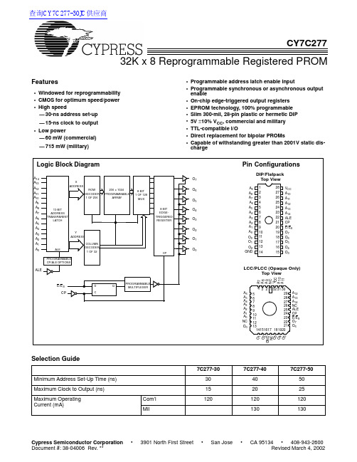
32K x 8 Reprogrammable Registered PROMCY7C277Features•Windowed for reprogrammability •CMOS for optimum speed/power •High speed—30-ns address set-up —15-ns clock to output •Low power—60 mW (commercial)—715 mW (military)•Programmable address latch enable input•Programmable synchronous or asynchronous output enable•On-chip edge-triggered output registers •EPROM technology, 100% programmable •Slim 300-mil, 28-pin plastic or hermetic DIP •5V ±10% V CC , commercial and military •TTL-compatible I/O•Direct replacement for bipolar PROMs•Capable of withstanding greater than 2001V static dis-chargePROGRAMMABLE MULTIPLEXERPROGRAMMABLE CP/ALE OPTIONSLogic Block DiagramPin Configurations123456789101112161718192024232221131425282726A 9A 8A 7A 6A 5A 4A 3A 2A 1A 0O 0O 1O 2GNDV CC A 10A 11A 12A 13A 14ALE CP E/E S O 7O 6O 4O 5O 312O 0314567891032130131415161726252423222111A 7V C C A 6A 5A 4A 3A 2A 1A 0A 13A 14NC CP O 7O 6O 5G N D LCC/PLCC (Opaque Only)A 12ALE A 8O 4O 2O 11819202728293215O 3A 9A 10A 11E/E S N C N C A 14A 13A 12A 11A 10A 9A 88-BIT 1OF 128MUXA 7A 6A 5A 4A 3A 2A 1A 0E/E SCP15-BIT ADDRESS TRANSPARENT/LATCH256x 1024PROGRAMMABLEARRAY8-BIT EDGE-TRIGGERED REGISTERROW DECODER 1OF 256ALE COLUMN DECODER 1OF 32ALECPD CQNC Top ViewDIP/Flatpack Top ViewYADDRESSXADDRESSO 7O 6O 5O 4O 3O 2O 1O 0Selection Guide7C277-307C277-407C277-50Minimum Address Set-Up Time (ns)304050Maximum Clock to Output (ns)152025Maximum Operating Current (mA)Com ’l 120120120Mil130130查询CY7C277-30JC供应商Functional DescriptionThe CY7C277 is a high-performance 32K word by 8-bit CMOS PROMs. It is packaged in the slim 28-pin 300-mil package. The ceramic package may be equipped with an erasure win-dow; when exposed to UV light, the PROM is erased and can then be reprogrammed. The memory cells utilize proven EPROM floating-gate technology and byte-wide algorithms. The CY7C277 offers the advantages of low power, superior performance, and high programming yield. The EPROM cell requires only 12.5V for the supervoltage and low current re-quirements allow for gang programming. The EPROM cells allow for each memory location to be 100% tested, as each location is written into, erased, and repeatedly exercised prior to encapsulation. Each PROM is also tested for AC perfor-mance to guarantee that the product will meet DC and AC specification limits after customer programming.On the 7C277, the outputs are pipelined through a mas-ter-slave register. On the rising edge of CP, data is loaded into the 8-bit edge triggered output register. The E/E S input pro-vides a programmable bit to select between asynchronous and synchronous operation. The default condition is asynchro-nous. When the asynchronous mode is selected, the E/E S pin operates as an asynchronous output enable. If the synchro-nous mode is selected, the E/E S pin is sampled on the rising edge of CP to enable and disable the outputs. The 7C277 also provides a programmable bit to enable the Address Latch in-put. If this bit is not programmed, the device will ignore the ALE pin and the address will enter the device asynchronously. If the ALE function is selected, the address enters the PROM while the ALE pin is active, and is captured when ALE is deasserted.The user may define the polarity of the ALE signal, with the default being active HIGH.Maximum Ratings(Above which the useful life may be impaired. For user guide-lines, not tested.)Storage Temperature ....................................−65°C to +150°C Ambient Temperature withPower Applied.................................................−55°C to +125°C Supply Voltage to Ground Potential.................−0.5V to +7.0V (Pin 24 to Pin 12)DC Voltage Applied to Outputsin High Z State.....................................................−0.5V to +7.0V DC Input Voltage.................................................−3.0V to +7.0V DC Program Voltage (Pins 7, 18, 20)...........................13.0V UV Erasure...................................................7258 Wsec/cm2 Static Discharge Voltage...........................................>2001V (per MIL-STD-883, Method 3015)Latch-Up Current.....................................................>200 mA Operating RangeRange Ambient Temperature V CC Commercial0°C to +70°C 5V ±10% Industrial[1]−40°C to +85°C 5V ±10% Military[2]−55°C to +125°C 5V ±10%Electrical Characteristics Over the Operating Range[3, 4]Parameter7C277-307C277-40, 50 Description Test Conditions Min.Max.Min.Max.UnitV OH Output HIGH Voltage V CC = Min., I OH = − 2.0 mA 2.4 2.4V V OL Output LOW Voltage V CC = Min., I OL = 8.0 mA0.40.4V V IH Input HIGH Level Guaranteed Input Logical HIGHVoltage for All Inputs2.0V CC 2.0V CC VV IL Input LOW Level Guaranteed Input Logical LOWVoltage for All Inputs0.80.8VI IX Input Leakage Current GND < V IN < V CC−10+10−10+10µA V CD Input Clamp Diode Voltage Note 4I OZ Output Leakage Current0 < V OUT < V CC, Output Disabled[5]−40+40−40+40µA I OS Output Short Circuit Current V CC = Max., V OUT = 0.0V[6]−20−90−20−90mAI CC Power Supply Current V CC = Max., CS > V IHI OUT = 0 mA Commercial120120mA Military130V PP Programming Supply Voltage12131213V I PP Programming Supply Current5050mA V IHP Input HIGH Programming Voltage 3.0 3.0V V ILP Input LOW Programming Voltage0.40.4V Notes:1.Contact a Cypress representative for industrial temperature range specifications.2.T A is the “instant on” case temperature.3.See the last page of this specification for Group A subgroup testing information.4.See “Introduction to CMOS PROMs” in this Book for general information on testing.5.For devices using the synchronous enable, the device must be clocked after applying these voltages to perform this measurement.6.For test purposes, not more than one output at a time should be shorted. Short circuit test duration should not exceed 30 seconds.Capacitance [4]ParameterDescriptionTest ConditionsMax.Unit C IN Input Capacitance T A = 25°C, f = 1 MHz,V CC = 5.0V10pF C OUTOutput Capacitance10pFAC Test Loads and Waveforms [4]3.0V 5V OUTPUTR1 500ΩR2333Ω30pFINCLUDINGJIG AND SCOPEGND90%10%90%10%<5ns<5ns5V OUTPUTR1 500ΩR2333Ω5pF INCLUDINGJIG AND SCOPE(a)NormalLoad(b)HighZ LoadOUTPUT2.0V Equivalent to:TH É VENIN EQUIVALENT ALL INPUT PULSES(658Ω MIL)(403Ω MIL)(403Ω MIL)OUTPUT1.9VCommercial Military(658Ω MIL)200Ω250ΩCY7C277 Switching Characteristics Over the Operating Range [3, 4]7C277-307C277-407C277-50Parameter DescriptionMin.Max.Min.Max.Min.Max.Unit t AL Address Set-Up to ALE Inactive 51010ns t LA Address Hold from ALE Inactive 101015ns t LL ALE Pulse Width101015ns t SA Address Set-Up to Clock HIGH 304050ns t HA Address Hold from Clock HIGH 000ns t SES E S Set-Up to Clock HIGH 121515ns t HES E S Hold from Clock HIGH 51010ns t CO Clock HIGH to Output Valid 152025ns t PWC Clock Pulse Width152020ns t LZC [7]Output Valid from Clock HIGH 152030ns t HZC Output High Z from Clock HIGH 152030ns t LZE [8]Output Valid from E LOW 152030ns t HZE [8]Output High Z from E HIGH152030nsNotes:7.Applies only when the synchronous (E S ) function is used.8.Applies only when the asynchronous (E) function is used.Architecture Byte (8000)D7D0C 7C 6C 5C 4 C 3 C 2 C 1 C 0Architecture Configuration BitsArchitecture Bit Architecture Verify D 7 - D 0FunctionALE D 10 = DEFAULT Input Transparent 1 = PGMED Input Latched ALEP D 20 = DEFAULT ALE = Active HIGH 1 = PGMED ALE = Active LOWE/E SD 00 = DEFAULT Asynchronous Output Enable (E)1 = PGMEDSynchronous Output Enable (E S )Bit MapProgrammer Address(Hex.)RAM Data 0000...7FFF 8000Data ...Data Control ByteNote:9.ALE is shown with positive polarity.t HZEt LZEt SES t SES t LZCt HZCt COt HES t HES HIGH ZHIGHZt ALt LAt LLt SAt HAA 0-A 14ALEE S(SYNCH)CPO 0-O 7E S(ASYNCH)t PWCt PWC Timing Diagram (Input Latched)[9]t LZEt HZEt SES t HZCTiming Diagram (Input Transparent)t SES t LZCt COt HES t HES HIGH ZHIGHZt SAt HAA 0-A 14E S(SYNCH)CPO 0-O 7E S(ASYNCH)t PWCt PWCProgramming InformationProgramming support is available from Cypress as well as from a number of third-party software vendors. For detailed programming information, including a listing of software pack-ages, please see the PROM Programming Information located at the end of this section. Programming algorithms can be ob-tained from any Cypress representative.Table 1.Mode SelectionPin Function [10]Read or Output DisableA 14–A 0E, E S CP ALE O 7–O 0Mode OtherA 14–A 0VFY PGM V PP D 7–D 0ReadA 14–A 0V IL V IH V IL O 7–O 0Output Disable A 14–A 0V IH X X High Z Program A 14–A 0V IHP V ILP V PP D 7–D 0Program Verify A 14–A 0V ILP V IHP /V ILP V PP O 7–O 0Program Inhibit A 14–A 0V IHP V IHP V PP High Z Blank CheckA 14–A 0V ILPV IHP /V ILPV PPO 7–O 0Note:10.X = “don ’t care ” but not to exceed V CC ±5%.Figure 1.Programming Pinouts123456789101112161718192024232221131425282726A 9A 8A 7A 6A 5A 4A 3A 2A 1A 0D 0D 1D 2GNDV CC A 10A 11A 12A 13A 14V PP PGM VFY D 7D 6D 4D 5D 312D 0314567891032130131415161726252423222111A 7V C C A 6A 5A 4A 3A 2A 1A 0PGM NC D 7D 6D 4VFY D 3D 2D 118192027282932N C N C D 5NC 15V PP DIP LCC/PLCC (Opaque Only)Top ViewTop ViewG N D A 12A 13A 14A 8A 9A 10A 11Typical DC and AC Characteristics1.41.61.00.84.0 4.55.05.56.0−55251251.21.1SUPPLYVOLTAGE (V)NORMALIZED SUPPLY CURRENT vs. SUPPLY VOLTAGENORMALIZED SUPPLY CURRENT vs. AMBIENT TEMPERATUREAMBIENTTEMPERATURE (°C)0.61.2N O R M A L I Z E D A C C E S S T I M E1501751257550250.01.02.03.0O U T P U T S I N K C U R R E N T (m A )0100OUTPUT VOLTAGE (V)OUTPUT SINK CURRENT vs. OUTPUT VOLTAGE1.00.90.8N O R M A L I Z E D I C CN O R M A L I Z E D I C CV CC =5.0V T A =25°C60504030201001.02.03.0O U T P U T S O U R C E C U R R E N T (m A )OUTPUT VOLTAGE (V)30.025.020.015.010.05.00200400600800D E L T A t (n s )A ACAPACITANCE (pF)TYPICAL ACCESS TIME CHANGEvs. OUTPUT LOADING4.00.01000T A =25°C V CC =4.5VT A =25°Cf =f MAX0OUTPUT SOURCE CURRENT vs. VOLTAGE 4.01.61.41.21.00.8−55125N O R M A L I Z E D S E T -U P T I M E0.625AMBIENT TEMPERATURE (°C)NORMALIZED SET-UP TIME vs. TEMPERATURE1.24.04.55.05.56.00.4SUPPLYVOLTAGE (V)NORMALIZED ACCESS TIME vs. SUPPLY VOLTAGET A =25°C1.00.80.6C277-12MILITARY SPECIFICATIONS Group A Subgroup Testing Ordering Information [11]Speed (ns)Ordering Code Package Name Package TypeOperating Range 30CY7C277-30JC J6532-Lead Plastic Leaded Chip Carrier CommercialCY7C277-30PC P2128-Lead (300-Mil) Molded DIP CY7C277-30WCW2228-Lead (300-Mil) Windowed CerDIP 40CY7C277-40JC J6532-Lead Plastic Leaded Chip Carrier Commercial CY7C277-40PC P2128-Lead (300-Mil) Molded DIP CY7C277-40WC W2228-Lead (300-Mil) Windowed CerDIP CY7C277-40DMB D2228-Lead (300-Mil) CerDIP Military CY7C277-40KMB K7428-Lead Rectangular CerpackCY7C277-40LMB L5532-Pin Rectangular Leadless Chip CarrierCY7C277-40QMB Q5532-Pin Windowed Rectangular Leadless Chip Carrier CY7C277-40TMB T7428-Lead Windowed Cerpack CY7C277-40WMBW2228-Lead (300-Mil) Windowed CerDIP 50CY7C277-50JC J6532-Lead Plastic Leaded Chip Carrier Commercial CY7C277-50PC P2128-Lead (300-Mil) Molded DIP CY7C277-50WC W2228-Lead (300-Mil) Windowed CerDIP CY7C277-50DMB D2228-Lead (300-Mil) CerDIP Military CY7C277-50KMB K7428-Lead Rectangular CerpackCY7C277-50LMB L5532-Pin Rectangular Leadless Chip CarrierCY7C277-50QMB Q5532-Pin Windowed Rectangular Leadless Chip Carrier CY7C277-50TMB T7428-Lead Windowed Cerpack CY7C277-50WMBW2228-Lead (300-Mil) Windowed CerDIPNote:11.Most of the above products are available in industrial temperature range. Contact a Cypress representative for specifications and productavailability.DC CharacteristicsParameterSubgroups V OH 1, 2, 3V OL 1, 2, 3V IH 1, 2, 3V IL 1, 2, 3I IX 1, 2, 3I OZ 1, 2, 3I CC1, 2, 3Switching CharacteristicsParameterSubgroups t SA 7, 8, 9, 10, 11t HA 7, 8, 9, 10, 11t CO7, 8, 9, 10, 11Package Diagrams28-Lead(300-Mil)CerDIP D22MIL-STD-1835D-15Config. A51-8003232-Lead Plastic Leaded Chip Carrier J6551-85002-B28-Lead Rectangular Cerpack K74MIL-STD-1835F-11 Config. A51-80061Package Diagrams (continued)32-Pin Rectangular Leadless Chip Carrier L55MIL-STD-1835 C-1251-8006851-85014-B28-Lead (300-Mil)Molded DIP P21Document #: 38-04006 Rev. **Page 11 of 13Package Diagrams (continued)MIL-STD-1835 C-1251-80103-*A 32-Pin Windowed Rectangular Leadless Chip Carrier Q55Document #: 38-04006 Rev. **Page 12 of 13© Cypress Semiconductor Corporation, 2002. The information contained herein is subject to change without notice. Cypress Semiconductor Corporation assumes no responsibility for the use of any circuitry other than circuitry embodied in a Cypress Semiconductor product. Nor does it convey or imply any license under patent or other rights. Cypress Semiconductor does not authorize its products for use as critical components in life-support systems where a malfunction or failure may reasonably be expected to result in significant injury to the user. The inclusion of Cypress Semiconductor products in life-support systems application implies that the manufacturer assumes all risk of such use and in doing so indemnifies Cypress Semiconductor against all charges.Package Diagrams (continued)Document #: 38-04006 Rev. **Page 13 of 13Document Title: CY7C277 32K x 8 Programmable Registered PROM Document Number: 38-04006REV.ECN NO.Issue Date Orig. of Change Description of Change **1138623/8/02DSG Change from Spec number: 38-00085 to 38-04006。
OpenCNC_PLC发展工具操作手册说明书

OpenCNC_PLC发展工具操作手册匯出日期:2023-12-19修改日期:2020-08-03PLC编辑器操作介绍Ladder编写开发PLC元件介绍1.2.•••• a.i.1 PLC 編輯器介绍1.1 软体下载进入新代网站 ,完成线上注册手续并確定權限開通。
至『下载中心』 => 『04.应用工具』 => 『Ladder Editor 』下载PLC 編輯器。
1.2 软体安装2.26.3(含)以前為安裝版执行LadEdit_vx.xx.x.msi 并依画面指示,即可完成安装程序。
安装完成後,依序点选『开始』 => 『程式集』 => 『OpenCNC 』 => 『MLCEdit.exe 』,即可开启PLC 編輯器。
2.29.0(含)以後為免安裝版第一次执行时:下载完LadEditor_x.xx.x.zip ,解压缩後右键点击『Install.bat 』,选择『以系统管理员身分执行』,将.lad 档的预设开启程式设定为PLC 編輯器ii.b.c.i.ii.•••••••執行『MLCEdit.exe』开启PLC編輯器第二次之後执行:執行『MLCEdit.exe』,或直接双击.lad档,皆可开启PLC編輯器注意事項:搬移免安装包位置時,請再次執行免安裝包內的『Install.bat』,否則會無法正常開啟.lad檔。
下載新版本PLC編輯器時,請執行新版本免安裝包內的『Install.bat』,否則仍會以舊版PLC編輯器開檔。
1.3 介面操作PLC編輯器介面共有七个区域,如下图所示:下拉式功能区指令按钮功能区指令区程式管理区指令编辑区元件注解区元件索引区下拉式功能区指令按钮功能区指令区指令区提供各种元件讓使用者選取、應用,详细说明请参阅後续章节。
程式管理区显示目前档案中的主程式及副程式指令编辑区編輯階梯圖內容之區塊参数输入栏选择指令元件後,在指令编辑区之适当位置按滑鼠左键,会出现如下图所示之元件参数设定视窗,在输入适当数值後,按下确认按钮,指令元件就會被寫入到指定位置。
单片机说明书
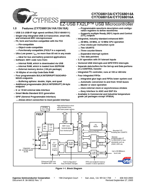
•
San Jose, CA 95134-1709 • 408-943-2600 Revised September 27, 2005
CY7C68013A/CY7C68014A CY7C68015A/CY7C68016A
1.1 Features (CY7C68013A/14A only)
USB 2.0 SIE or external transceiver implementations. With EZ-USB FX2LP, the Cypress Smart SIE handles most of the USB 1.1 and 2.0 protocol in hardware, freeing the embedded microcontroller for application-specific functions and decreasing development time to ensure USB compatibility. The General Programmable Interface (GPIF) and Master/Slave Endpoint FIFO (8- or 16-bit data bus) provides an easy and glueless interface to popular interfaces such as ATA, UTOPIA, EPP, PCMCIA, and most DSP/processors. The FX2LP draws considerably less current than the FX2 (CY7C68013), has double the on-chip code/data RAM and is fit, form and function compatible with the 56-, 100-, and 128pin FX2. Five packages are defined for the family: 56VFBGA, 56 SSOP, 56 QFN, 100 TQFP, and 128 TQFP.
CY7C1460AV33资料
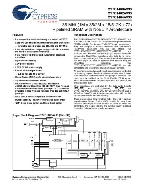
36-Mbit (1M x 36/2M x 18/512K x 72)Pipelined SRAM with NoBL™ ArchitectureCY7C1460AV33CY7C1462AV33CY7C1464AV33Features•Pin-compatible and functionally equivalent to ZBT™ •Supports 250-MHz bus operations with zero wait states —Available speed grades are 250, 200 and 167 MHz •Internally self-timed output buffer control to eliminate the need to use asynchronous OE•Fully registered (inputs and outputs) for pipelined operation•Byte Write capability •3.3V power supply •3.3V/2.5V I/O power supply •Fast clock-to-output times —2.6 ns (for 250-MHz device)•Clock Enable (CEN) pin to suspend operation •Synchronous self-timed writes•CY7C1460AV33, CY7C1462AV33 available inJEDEC-standard lead-free 100-pin TQFP , lead-free and non-lead-free 165-ball FBGA package. CY7C1464AV33 available in lead-free and non-lead-free 209-ball FBGA package•IEEE 1149.1 JTAG-Compatible Boundary Scan •Burst capability—linear or interleaved burst order •“ZZ” Sleep Mode option and Stop Clock optionFunctional DescriptionThe CY7C1460AV33/CY7C1462AV33/CY7C1464AV33 are 3.3V, 1M x 36/2M x 18/512K x72 Synchronous pipelined burst SRAMs with No Bus Latency™ (NoBL ™) logic, respectively.They are designed to support unlimited true back-to-back Read/Write operations with no wait states. The CY7C1460AV33/CY7C1462AV33/CY7C1464AV33 are equipped with the advanced (NoBL) logic required to enable consecutive Read/Write operations with data being trans-ferred on every clock cycle. This feature dramatically improves the throughput of data in systems that require frequent Write/Read transitions. The CY7C1460AV33/CY7C1462AV33/CY7C1464AV33 are pin compatible and functionally equivalent to ZBT devices.All synchronous inputs pass through input registers controlled by the rising edge of the clock. All data outputs pass through output registers controlled by the rising edge of the clock. The clock input is qualified by the Clock Enable (CEN) signal,which when deasserted suspends operation and extends the previous clock cycle.Write operations are controlled by the Byte Write Selects (BW a –BW h for CY7C1464AV33, BW a –BW d for CY7C1460AV33 and BW a –BW b for CY7C1462AV33) and a Write Enable (WE) input. All writes are conducted with on-chip synchronous self-timed write circuitry.Three synchronous Chip Enables (CE 1, CE 2, CE 3) and an asynchronous Output Enable (OE) provide for easy bank selection and output tri-state control. In order to avoid bus contention, the output drivers are synchronously tri-stated during the data portion of a write sequence.Selection Guide250 MHz200 MHz167 MHz Unit Maximum Access Time 2.6 3.2 3.4ns Maximum Operating Current475425375mA120120120mA Maximum CMOS StandbyCurrentPin ConfigurationsA A A A A 1A 0V S SV D DA A A A A AV DDQ V SS DQb DQb DQb V SSV DDQDQb DQb V SSNCV DDDQaDQa V DDQ V SSDQa DQa V SS V DDQ V DDQV SS DQc DQc V SS V DDQ DQc V DD V SS DQd DQd V DDQ V SS DQd DQd DQd V SS V DDQ A A C E 1C E 2B W aC E 3V D DV S SC L K W E C E N O E A A123456789101112131415161718192021222324252627282930313233343536373839404142434445464748495080797877767574737271706968676665646362616059585756555453525110099989796959493929190898887868584838281A AA D V /L D ZZCY7C1460AV33100-pin TQFP PinoutA A A A A 1A 0V S SV D DA A A A A AA NC NC V DDQ V SS NC DQPa DQa DQa V SS V DDQ DQa DQa V SS NC V DD DQa DQa V DDQ V SS DQa DQa NC NC V SS V DDQ NC NC NCNC NC NC V DDQ V SSNC NC DQb DQbV SS V DDQ DQb DQbV DD V SS DQb DQb V DDQV SS DQb DQb DQPb NC V SS V DDQNC NC NCA A C E 1C E 2N C N C B W b B W a C E 3V D DV S SC L K W E C E N O E A A123456789101112131415161718192021222324252627282930313233343536373839404142434445464748495080797877767574737271706968676665646362616059585756555453525110099989796959493929190898887868584838281A AA D V /L D ZZ M O D E CY7C1462AV33B W d M O D E B W c DQc DQc DQc DQc DQPc DQd DQd DQd DQPbDQbDQa DQaDQa DQa DQPa DQbDQb(1M × 36)(2M × 18)B W b NC NC NC DQc NC N C /288MN C /144MN C /72MN C /288MN C /144MN C /72MDQPdA A A APin Configurations (continued)234567 1ABCDEFGHJKLMNP RTDONC/576MNC/1GDQP cDQ cDQP dNCDQ dA CE1BW b CE3BW c CENA CE2DQ cDQ dDQ dMODENCDQ cDQ cDQ dDQ dDQ dNC/72MV DDQBW d BW a CLK WEV SS V SS V SS V SSV DDQ V SSV DD V SSV SSV SSNCV SSV SSV SSV SSV DDQV DDQNCV DDQV DDQV DDQV DDQAAV DD V SSV DD V SS V SSV DDQ V DDV SSV DDV SSV DD V SS V SSV SSV DDV DD V SSV DD V SS V SSNCTCKA0V SSTDIAADQ c V SSDQ c V SSDQ cDQ cNCV SSV SSV SSV SSNCV SSA1DQ dDQ dNC/144MNCV DDQV SSTMS891011NC/288MA AADV/LD NCOE A A NCV SS V DDQ NC DQP bV DDQV DD DQ bDQ bDQ bNCDQ bNCDQ aDQ aV DD V DDQV DD V DDQ DQ bV DDNCV DDDQ aV DD V DDQ DQ aV DDQV DDV DD V DDQV DD V DDQ DQ aV DDQAAV SSAAADQ bDQ bDQ bZZDQ aDQ aDQP aDQ aAV DDQA2345671A B C D E F G H J K L M NP RTDONC/576MNC/1GNCNCDQP bNCDQ bA CE1CE3BW b CENA CE2NCDQ bDQ bMODENCDQ bDQ bNCNCNCNC/72MV DDQBW a CLK WEV SS V SS V SS V SSV DDQ V SSV DD V SSV SSV SSNCV SSV SSV SSV SSV DDQV DDQNCV DDQV DDQV DDQV DDQAAV DD V SSV DD V SS V SSV DDQ V DDV SSV DDV SSV DD V SS V SSV SSV DDV DD V SSV DD V SS V SSNCTCKA0V SSTDIAADQ b V SSNC V SSDQ bNCNCV SSV SSV SSV SSNCV SSA1DQ bNCNC/144MNCV DDQV SSTMS891011NC/288MA AADV/LDNCAOE A AV SS V DDQ NC DQP aV DDQV DD NCDQ aDQ aNCNCNCDQ aNCV DD V DDQV DD V DDQ DQ aV DDNCV DDNCV DD V DDQ DQ aV DDQV DDV DD V DDQV DD V DDQ NCV DDQAAV SSAAADQ aNCNCZZDQ aNCNCDQ aAV DDQACY7C1462AV33 (2M × 18)CY7C1460AV33 (1M × 36)165-ball FBGA (15 x 17 x 1.4 mm) PinoutAANCNCPin DefinitionsPin Name I/O Type Pin DescriptionA0 A1 AInput-SynchronousAddress Inputs used to select one of the address locations. Sampled at the risingedge of the CLK.BW a BW b BW c BW d BW e BW f BW g BW hInput-SynchronousByte Write Select Inputs, active LOW. Qualified with WE to conduct writes to the SRAM.Sampled on the rising edge of CLK. BW a controls DQ a and DQP a, BW b controls DQ b andDQP b, BW c controls DQ c and DQP c, BW d controls DQ d and DQP d, BW e controls DQ e andDQP e, BW f controls DQ f and DQP f, BW g controls DQ g and DQP g, BW h controls DQ h andDQP h.WE Input-Synchronous Write Enable Input, active LOW. Sampled on the rising edge of CLK if CEN is active LOW. This signal must be asserted LOW to initiate a write sequence.ADV/LD Input-Synchronous Advance/Load Input used to advance the on-chip address counter or load a new address. When HIGH (and CEN is asserted LOW) the internal burst counter is advanced. When LOW, a new address can be loaded into the device for an access. After being deselected, ADV/LD should be driven LOW in order to load a new address.Pin Configurations (continued)A B C D E F G H J K L M N P R T U V W1234567891110DQgDQgDQgDQgDQgDQgDQgDQgDQcDQcDQcDQcNCDQPgDQhDQhDQhDQhDQdDQdDQdDQdDQPdDQPcDQcDQcDQcDQcNCDQhDQhDQhDQhDQPhDQdDQdDQdDQdDQbDQbDQbDQbDQbDQbDQbDQbDQfDQfDQfDQfNCDQPfDQaDQaDQaDQaDQeDQeDQeDQeDQPaDQPbDQfDQfDQfDQfNCDQaDQaDQaDQaDQPeDQeDQeDQeDQeA A A ANC NCNC/144M NC/72M A NC/288MA A AA A A A1A0A A AA AANC/576MNCNCNC NCNCBWS b BWSfBWS e BWS aBWS c BWS gBWS dBWS hTMS TDI TDO TCKNCNC MODE NCCEN V SSNCCLK NC V SSV DD V DD V DDV DDV DDV DDV DDV DDV DDV DDV DDV DDV DDV SS V SSV SSV SSV SSV SS V SSV SSNC/1GV DDNCOECE3CE1CE2ADV/LDWEV SSV SSV SSV SS V SS V SS V SSZZV SS V SS V SS V SSNCV DDQV SSV SS NC V SS V SSV SS V SS VSSV SSNCV SSV DDQ V DDQ V DDQ V DDQV DDQ NC V DDQ VDDQV DDQ V DDQ NC V DDQ V DDQV DDQ V DDQ NC V DDQ VDDQV DDQV DDQV DDQ V DDQV DDQ VDDQV DDQ V DDQ209-ball FBGA (14 x 22 x 1.76 mm) PinoutCY7C1464AV33 (512K x 72)CLK Input-Clock Clock Input. Used to capture all synchronous inputs to the device. CLK is qualified with CEN. CLK is only recognized if CEN is active LOW.CE1Input-Synchronous Chip Enable 1 Input, active LOW. Sampled on the rising edge of CLK. Used in conjunction with CE2 and CE3 to select/deselect the device.CE2Input-Synchronous Chip Enable 2 Input, active HIGH. Sampled on the rising edge of CLK. Used in conjunction with CE1 and CE3 to select/deselect the device.CE3Input-Synchronous Chip Enable 3 Input, active LOW. Sampled on the rising edge of CLK. Used in conjunction with CE1 and CE2 to select/deselect the device.OE Input-Asynchronous Output Enable, active LOW. Combined with the synchronous logic block inside the device to control the direction of the I/O pins. When LOW, the I/O pins are allowed to behave as outputs. When deasserted HIGH, I/O pins are tri-stated, and act as input data pins. OE is masked during the data portion of a write sequence, during the first clock when emerging from a deselected state and when the device has been deselected.CEN Input-Synchronous Clock Enable Input, active LOW. When asserted LOW the clock signal is recognized by the SRAM. When deasserted HIGH the clock signal is masked. Since deasserting CEN does not deselect the device, CEN can be used to extend the previous cycle when required.DQ a DQ b DQ c DQ d DQ e DQ f DQ g DQ hI/O-SynchronousBidirectional Data I/O lines. As inputs, they feed into an on-chip data register that istriggered by the rising edge of CLK. As outputs, they deliver the data contained in thememory location specified by A X during the previous clock rise of the read cycle. Thedirection of the pins is controlled by OE and the internal control logic. When OE is assertedLOW, the pins can behave as outputs. When HIGH, DQ a–DQ d are placed in a tri-statecondition. The outputs are automatically tri-stated during the data portion of a writesequence, during the first clock when emerging from a deselected state, and when thedevice is deselected, regardless of the state of OE.DQP a,DQP b, DQP c,DQP d DQP e,DQP f DQP g,DQP hI/O-SynchronousBidirectional Data Parity I/O lines. Functionally, these signals are identical to DQ[31:0].During write sequences, DQP a is controlled by BW a, DQP b is controlled by BW b, DQP c iscontrolled by BW c, and DQP d is controlled by BW d, DQP e is controlled by BW e, DQP f iscontrolled by BW f, DQP g is controlled by BW g, DQP h is controlled by BW h.MODE Input Strap Pin Mode Input. Selects the burst order of the device. Tied HIGH selects the interleaved burstorder. Pulled LOW selects the linear burst order. MODE should not change states duringoperation. When left floating MODE will default HIGH, to an interleaved burst order. TDO JTAG serial outputSynchronousSerial data-out to the JTAG circuit. Delivers data on the negative edge of TCK.TDI JTAG serial inputSynchronousSerial data-In to the JTAG circuit. Sampled on the rising edge of TCK.TMS Test Mode SelectSynchronous This pin controls the Test Access Port state machine. Sampled on the rising edge of TCK.TCK JTAG-Clock Clock input to the JTAG circuitry.V DD Power Supply Power supply inputs to the core of the device.V DDQ I/O Power Supply Power supply for the I/O circuitry.V SS Ground Ground for the device. Should be connected to ground of the system. NC N/A No connects. This pin is not connected to the die.NC/72M N/A Not connected to the die. Can be tied to any voltage level.NC/144M N/A Not connected to the die. Can be tied to any voltage level.NC/288M N/A Not connected to the die. Can be tied to any voltage level.NC/576M N/A Not connected to the die. Can be tied to any voltage level.NC/1G N/A Not connected to the die. Can be tied to any voltage level.ZZ Input-Asynchronous ZZ “sleep” Input. This active HIGH input places the device in a non-time critical “sleep” condition with data integrity preserved. During normal operation, this pin can be connected to V SS or left floating. ZZ pin has an internal pull-down.Pin Definitions (continued)Pin Name I/O Type Pin DescriptionFunctional OverviewThe CY7C1460AV33/CY7C1462AV33/CY7C1464AV33 are synchronous-pipelined Burst NoBL SRAMs designed specifi-cally to eliminate wait states during Write/Read transitions. All synchronous inputs pass through input registers controlled by the rising edge of the clock. The clock signal is qualified with the Clock Enable input signal (CEN). If CEN is HIGH, the clock signal is not recognized and all internal states are maintained. All synchronous operations are qualified with CEN. All data outputs pass through output registers controlled by the rising edge of the clock. Maximum access delay from the clock rise (t CO) is 2.6 ns (250-MHz device).Accesses can be initiated by asserting all three Chip Enables (CE1, CE2, CE3) active at the rising edge of the clock. If Clock Enable (CEN) is active LOW and ADV/LD is asserted LOW, the address presented to the device will be latched. The access can either be a read or write operation, depending on the status of the Write Enable (WE). BW[x] can be used to conduct byte write operations.Write operations are qualified by the Write Enable (WE). All writes are simplified with on-chip synchronous self-timed write circuitry.Three synchronous Chip Enables (CE1, CE2, CE3) and an asynchronous Output Enable (OE) simplify depth expansion. All operations (Reads, Writes, and Deselects) are pipelined. ADV/LD should be driven LOW once the device has been deselected in order to load a new address for the next operation.Single Read AccessesA read access is initiated when the following conditions are satisfied at clock rise: (1) CEN is asserted LOW, (2) CE1, CE2, and CE3 are ALL asserted active, (3) the Write Enable input signal WE is deasserted HIGH, and (4) ADV/LD is asserted LOW. The address presented to the address inputs is latched into the Address Register and presented to the memory core and control logic. The control logic determines that a read access is in progress and allows the requested data to propagate to the input of the output register. At the rising edge of the next clock the requested data is allowed to propagate through the output register and onto the data bus within 2.6 ns (250-MHz device) provided OE is active LOW. After the first clock of the read access the output buffers are controlled by OE and the internal control logic. OE must be driven LOW in order for the device to drive out the requested data. During the second clock, a subsequent operation (Read/Write/Deselect) can be initiated. Deselecting the device is also pipelined. Therefore, when the SRAM is deselected at clock rise by one of the chip enable signals, its output will tri-state following the next clock rise.Burst Read AccessesThe CY7C1460AV33/CY7C1462AV33/CY7C1464AV33 have an on-chip burst counter that allows the user the ability to supply a single address and conduct up to four Reads without reasserting the address inputs. ADV/LD must be driven LOW in order to load a new address into the SRAM, as described in the Single Read Access section above. The sequence of the burst counter is determined by the MODE input signal. A LOW input on MODE selects a linear burst mode, a HIGH selects an interleaved burst sequence. Both burst counters use A0 and A1 in the burst sequence, and will wrap-around when incre-mented sufficiently. A HIGH input on ADV/LD will increment the internal burst counter regardless of the state of chip enables inputs or WE. WE is latched at the beginning of a burst cycle. Therefore, the type of access (Read or Write) is maintained throughout the burst sequence.Single Write AccessesWrite access are initiated when the following conditions are satisfied at clock rise: (1) CEN is asserted LOW, (2) CE1, CE2, and CE3 are ALL asserted active, and (3) the write signal WE is asserted LOW. The address presented to the address inputs is loaded into the Address Register. The write signals are latched into the Control Logic block.On the subsequent clock rise the data lines are automatically tri-stated regardless of the state of the OE input signal. This allows the external logic to present the data on DQ and DQP (DQ a,b,c,d,e,f,g,h/DQP a,b,c,d,e,f,g,h for CY7C1464AV33, DQ a,b,c,d/DQP a,b,c,d for CY7C1460AV33 and DQ a,b/DQP a,b for CY7C1462AV33). In addition, the address for the subse-quent access (Read/Write/Deselect) is latched into the Address Register (provided the appropriate control signals are asserted).On the next clock rise the data presented to DQ and DQP (DQ a,b,c,d,e,f,g,h/DQP a,b,c,d,e,f,g,h for CY7C1464AV33, DQ a,b,c,d/DQP a,b,c,d for CY7C1460AV33 & DQ a,b/DQP a,b for CY7C1462AV33) (or a subset for byte write operations, see Write Cycle Description table for details) inputs is latched into the device and the write is complete.The data written during the Write operation is controlled by BW (BW a,b,c,d,e,f,g,h for CY7C1464AV33, BW a,b,c,d for CY7C1460AV33 and BW a,b for CY7C1462AV33) signals. The CY7C1460AV33/CY7C1462AV33/CY7C1464AV33 provides byte write capability that is described in the Write Cycle Description table. Asserting the Write Enable input (WE) with the selected Byte Write Select (BW) input will selectively write to only the desired bytes. Bytes not selected during a byte write operation will remain unaltered. A synchronous self-timed write mechanism has been provided to simplify the write operations. Byte write capability has been included in order to greatly simplify Read/Modify/Write sequences, which can be reduced to simple byte write operations.Because the CY7C1460AV33/CY7C1462AV33/CY7C1464AV33 are common I/O devices, data should not be driven into the device while the outputs are active. The Output Enable (OE) can be deasserted HIGH before presenting data to the DQ and DQP (DQ a,b,c,d,e,f,g,h/DQP a,b,c,d,e,f,g,h for CY7C1464AV33, DQ a,b,c,d/DQP a,b,c,d for CY7C1460AV33 and DQ a,b/DQP a,b for CY7C1462AV33) inputs. Doing so will tri-state the output drivers. As a safety precaution, DQ and DQP (DQ a,b,c,d,e,f,g,h/DQP a,b,c,d,e,f,g,h for CY7C1464AV33, DQ a,b,c,d/DQP a,b,c,d for CY7C1460AV33 and DQ a,b/DQP a,b for CY7C1462AV33) are automatically tri-stated during the data portion of a write cycle, regardless of the state of OE. Burst Write AccessesThe CY7C1460AV33/CY7C1462AV33/CY7C1464AV33 has an on-chip burst counter that allows the user the ability to supply a single address and conduct up to four WRITE opera-tions without reasserting the address inputs. ADV/LD must be driven LOW in order to load the initial address, as described in the Single Write Access section above. When ADV/LD is driven HIGH on the subsequent clock rise, the chip enables (CE1, CE2, and CE3) and WE inputs are ignored and the burstcounter is incremented. The correct BW (BW a,b,c,d,e,f,g,h for CY7C1464AV33, BW a,b,c,d for CY7C1460AV33 and BW a,b for CY7C1462AV33) inputs must be driven in each cycle of the burst write in order to write the correct bytes of data.Sleep ModeThe ZZ input pin is an asynchronous input. Asserting ZZ places the SRAM in a power conservation “sleep” mode. Two clock cycles are required to enter into or exit from this “sleep”mode. While in this mode, data integrity is guaranteed. Accesses pending when entering the “sleep” mode are not considered valid nor is the completion of the operation guaranteed. The device must be deselected prior to entering the “sleep” mode. CE1, CE2, and CE3, must remain inactive for the duration of t ZZREC after the ZZ input returns LOW.Interleaved Burst Address Table(MODE = Floating or V DD)FirstAddressSecondAddressThirdAddressFourthAddress A1,A0A1,A0A1,A0A1,A000011011010011101011000111100100 Linear Burst Address Table (MODE = GND)FirstAddressSecondAddressThirdAddressFourthAddress A1,A0A1,A0A1,A0A1,A000011011011011001011000111000110ZZ Mode Electrical CharacteristicsParameter Description Test Conditions Min.Max.Unit I DDZZ Sleep mode standby current ZZ > V DD − 0.2V100mA t ZZS Device operation to ZZ ZZ > V DD− 0.2V2t CYC ns t ZZREC ZZ recovery time ZZ < 0.2V2t CYC ns t ZZI ZZ active to sleep current This parameter is sampled2t CYC ns t RZZI ZZ Inactive to exit sleep current This parameter is sampled0nsTruth Table[1, 2, 3, 4, 5, 6, 7]Operation AddressUsed CE ZZ ADV/LD WE BW x OE CEN CLK DQDeselect Cycle None H L L X X X L L-H Tri-State ContinueDeselect CycleNone X L H X X X L L-H Tri-StateRead Cycle(Begin Burst)External L L L H X L L L-H Data Out (Q)Read Cycle(Continue Burst)Next X L H X X L L L-H Data Out (Q)NOP/Dummy Read(Begin Burst)External L L L H X H L L-H Tri-StateDummy Read(Continue Burst)Next X L H X X H L L-H Tri-StateNotes:1.X = “Don't Care”, H = Logic HIGH, L = Logic LOW, CE stands for ALL Chip Enables active. BWx = L signifies at least one Byte Write Select is active, BWx =Valid signifies that the desired byte write selects are asserted, see Write Cycle Description table for details.2.X. See Write Cycle Description table for details.3.When a write cycle is detected, all I/Os are tri-stated, even during byte writes.4.The DQ and DQP pins are controlled by the current cycle and the OE signal.5.6.Device will power-up deselected and the I/Os in a tri-state condition, regardless of OE.7.OE is asynchronous and is not sampled with the clock rise. It is masked internally during write cycles.During a read cycle DQ s and DQP Xis inactive or when the device is deselected, and DQ s=data when OE is active.Write Cycle (Begin Burst)External L L L L L X L L-H Data In (D)Write Cycle(Continue Burst)Next X L H X L X L L-H Data In (D)NOP/WRITE ABORT (Begin Burst)None L L L L H X L L-H Tri-State WRITE ABORT (Continue Burst)Next X L H X H X L L-H Tri-StateIGNORE CLOCK EDGE (Stall)Current X L X X X X H L-H -SLEEP MODENoneXHXXXXXXTri-StateTruth Table [1, 2, 3, 4, 5, 6, 7] (continued)Operation Address Used CE ZZ ADV/LDWE BW x OE CEN CLKDQ Partial Write Cycle Description [1, 2, 3, 8]Function (CY7C1460AV33)WE BW d BW c BW b BW a ReadH X X X X Write – No bytes written L H H H H Write Byte a – (DQ a and DQP a )L H H H L Write Byte b – (DQ b and DQP b )L H H L H Write Bytes b, aL H H L L Write Byte c – (DQ c and DQP c )L H L H H Write Bytes c, a L H L H L Write Bytes c, b L H LL L H Write Bytes c, b, aL H L L L Write Byte d – (DQ d and DQP d )L L H H H Write Bytes d, a L L H H L Write Bytes d, b L L H L H Write Bytes d, b, a L L H L L Write Bytes d, c L L L H H Write Bytes d, c, a L L L H L Write Bytes d, c, b L L L L H Write All BytesLL LLL Function (CY7C1462AV33)[2,8]WE BW b BW a ReadH x x Write – No Bytes Written L H H Write Byte a – (DQ a and DQP a )L H L Write Byte b – (DQ b and DQP b )L L H Write Both BytesLLL Function (CY7C1464AV33)[2,8]WE BW x ReadH x Write – No Bytes Written L H Write Byte X − (DQ x and DQP x)L L Write All BytesL All BW = LNote:8.[a:d] is valid. Appropriate write will be done based on which byte write is active.IEEE 1149.1 Serial Boundary Scan (JTAG)The CY7C1460AV33/CY7C1462AV33/CY7C1464AV33 incor-porates a serial boundary scan test access port (TAP). This part is fully compliant with 1149.1. The TAP operates using JEDEC-standard 3.3V or 2.5V I/O logic level.The CY7C1460AV33/CY7C1462AV33/CY7C1464AV33 contains a TAP controller, instruction register, boundary scan register, bypass register, and ID register.Disabling the JTAG FeatureIt is possible to operate the SRAM without using the JTAG feature. To disable the TAP controller, TCK must be tied LOW (V SS) to prevent clocking of the device. TDI and TMS are inter-nally pulled up and may be unconnected. They may alternately be connected to V DD through a pull-up resistor. TDO should be left unconnected. Upon power-up, the device will come up in a reset state which will not interfere with the operation of the device.TAP Controller State DiagramThe 0/1 next to each state represents the value of TMS at the rising edge of TCK.Test Access Port (TAP)Test Clock (TCK)The test clock is used only with the TAP controller. All inputs are captured on the rising edge of TCK. All outputs are driven from the falling edge of TCK.Test MODE SELECT (TMS)The TMS input is used to give commands to the TAP controller and is sampled on the rising edge of TCK. It is allowable to leave this ball unconnected if the TAP is not used. The ball is pulled up internally, resulting in a logic HIGH level.Test Data-In (TDI)The TDI ball is used to serially input information into the registers and can be connected to the input of any of the registers. The register between TDI and TDO is chosen by the instruction that is loaded into the TAP instruction register. TDI is internally pulled up and can be unconnected if the TAP is unused in an application. TDI is connected to the most signif-icant bit (MSB) of any register. (See Tap Controller Block Diagram.)Test Data-Out (TDO)The TDO output ball is used to serially clock data-out from the registers. The output is active depending upon the current state of the TAP state machine. The output changes on the falling edge of TCK. TDO is connected to the least significant bit (LSB) of any register. (See Tap Controller State Diagram.) TAP Controller Block DiagramPerforming a TAP ResetA RESET is performed by forcing TMS HIGH (VDD) for five rising edges of TCK. This RESET does not affect the operation of the SRAM and may be performed while the SRAM is operating.At power-up, the TAP is reset internally to ensure that TDO comes up in a High-Z state.TAP RegistersRegisters are connected between the TDI and TDO balls and allow data to be scanned into and out of the SRAM test circuitry. Only one register can be selected at a time through the instruction register. Data is serially loaded into the TDI ball on the rising edge of TCK. Data is output on the TDO ball on the falling edge of TCK.Instruction RegisterThree-bit instructions can be serially loaded into the instruction register. This register is loaded when it is placed between the TDI and TDO balls as shown in the Tap Controller Block Diagram. Upon power-up, the instruction register is loaded with the IDCODE instruction. It is also loaded with the IDCODE instruction if the controller is placed in a reset state as described in the previous section.。
HK32C005 数据手册说明书
HK32C005数据手册版本:1.3发布日期:2023-08-15深圳市航顺芯片技术研发有限公司前言前言编写目的本文档介绍了HK32C005系列芯片的结构框图、存储器映射、外设接口、电气特性、引脚封装等,旨在帮助用户快速了解该系列芯片的特点及功能。
读者对象本文适用于以下读者:•开发工程师•芯片测试工程师•芯片选型工程师版本说明本文档对应的产品系列为HK32C005系列芯片。
修订记录目录1 简介 (1)2 产品概述 (2)2.1 产品特性 (3)2.2 器件一览表 (4)3 功能介绍 (6)3.1 结构框图 (6)3.2 存储器映射 (7)3.3 存储器 (7)3.3.1 Flash (7)3.3.2 内置SRAM (7)3.4 CRC计算单元 (7)3.5 供电方案 (8)3.6 电源监控器 (8)3.7 复位 (8)3.7.1 系统复位 (8)3.7.2 电源复位 (9)3.7.3 备份域复位 (9)3.8 时钟和时钟树 (9)3.9 SYSCFG (10)3.10 GPIO (10)3.11 Boot模式 (10)3.12 低功耗模式 (10)3.13 中断与事件 (10)3.13.1 NVIC (10)3.13.2 EXTI (11)3.14 独立看门狗(IWDG) (11)3.15 窗口看门狗(WWDG) (11)3.16 定时器 (11)3.16.1 高级定时器 (12)3.16.2 通用定时器 (12)3.17 DMA (13)3.18 ADC (13)3.18.1 内部参考电压 (13)3.19 温度传感器 (13)3.20 红外遥控接口(IRTIM) (13)3.21 I2C总线 (14)3.22 通用异步收发器(UART) (14)3.23 串行外设接口(SPI/I2S) (14)3.24 RTC (15)3.25 DVSQ计算单元 (15)3.26 96位UID (16)3.27 调试接口 (16)4 电气性能指标 (17)4.1 最大绝对额定值 (17)4.1.1 极限电压特性 (17)4.1.2 极限电流特性 (17)4.1.3 极限温度特性 (17)4.2 工作参数 (18)4.2.1 推荐工作条件 (18)4.2.2 低压检测 (18)4.2.3 上/下电复位特性 (18)4.2.4 内部参考电压 (18)4.2.5 工作电流特性 (19)4.2.6 外部高速(HSE)时钟特性 (20)4.2.7 内部高速(HSI)时钟特性 (20)4.2.8 内部低速(LSI)时钟特性 (21)4.2.9 PLL特性 (21)4.2.10 Flash存储器特性 (21)4.2.11 IO输入引脚特性 (21)4.2.14 TIM计数器特性 (22)4.2.15 ADC特性 (22)4.2.16 温度传感器特性 (24)5 典型电路 (26)5.1 电源供电 (26)6 引脚定义 (27)6.1 LQFP32封装 (27)6.2 LQFP32封装的引脚定义 (27)6.3 引脚复用(AF)功能表 (32)7 封装参数 (33)7.1 LQFP32封装 (33)7.2 LQFP32丝印 (34)8 订货信息 (35)8.1 订货代码 (35)8.2 订货包装 (35)9 缩略语与术语 (36)9.1 缩略语 (36)9.2 术语 (36)10 重要提示 (37)1简介本文档为HK32C005系列芯片的数据手册。
CM108芯片基于USB音频遥控器修改指南说明书

Modifying a USB sound fob to act as a repeater interface for app_rptRev E 9/13/2008This document explains how to modify a USB sound f ob to work as a repeater interface for app_rpt. For a guide on setting up and configuring Asterisk, app_rpt, and chan_usbradio.c please see http://app/usbradio.pdfThe following materials and tools are required:B sound f ob based on the CM108 chip2.10K ohm 1/8W 5% through hole resistor. Digi Key P/N 10KEBKND3.68K ohm 1/8W 5% through hole resistor. Digi Key P/N 68KEBKND4.470K ohm 1/8W 5% through hole resistor. Digi Key P/N 470KEBKND5.Two 10 microfarad 25V nonpolarized electrolytic capacitors. Digi Key P1176ND6.BAT43 or equivalent schottky diode in DO35 pac kage. Digi Key 49724921ND7.2N4401 NPN bipolar transistor in a TO92 package. Digi Key 2N4401ND8.Plastic sleeving and heat shrink tubing9.Hot melt glue and glue gun10.Male Dsub connector and hood11.1ft. of 5 conductor shielded cable with 28awg stranded wires or smaller.12.Temperature controlled Soldering iron with a fine tip, and 0.020” diameter solder13. Precision cutters and long nose pliers.Below is a picture of a typical USB sound fob. This is one which was purchased for $7.95. When shopping for a suitable sound fob, it is important to purchase one which uses the CM108 chip, as that is the only version supported.The first thing to do is open up the case. The case is usually pressfit together with four plastic posts on one side and 4 sockets for the posts on the other side. Getting the case to come apart requires a small thin bladed screwdriver. Work the screwdriver along the seams until one side starts to separate, then work on the other side. Be very careful with the use of downward pressure. Y ou don't want the screwdriver going in and damaging the components on the board. Pry the case open near the audio jacks since they will be removed anyway. Once the case is separated, you should have something like this:Peel the QC sticker off the chip and verify it is a CM108. If it isn't a CM108, it cannot be used. Then using a pair of precision cutters, remove the 3.5mm jacks by cutting the metal connections on the side of the jack as shown:Once the connections are free on the outsides of each jack, rock them back and forth to cause the inner connections to break free as shown:When both jacks are removed, your board should look like this:Do not be tempted to clean out the pins from the holes used b y the jacks, The traces on the board lift very easily.Prepare one end of the 5 conductor cable by separating the shield, twisting it tightly, then soldering it to the ground on the board below as shown. The shield is soldered to the point where the sleeve contact of the microphone jack used to connect.Now we connect some wires to points on the board. For the multiconductor cable I'm using, white is receive audio, black is transmit audio, brown is auxiliary audio, red is PTT, and green is COR. For now we will solder down the receive audio (white), transmit audio (black) , and auxiliary audio (brown) wires as shown:Note that the rxaudio (white) lead is connected to the middle pin of the mic connector at the top.Next, we add the 10K resistor shown prepped abo ve with some plastic tubing to pin 13 of the CM108. Toget access to pin 13 on this particular board, I had to temporarily bend the crystal up and out of the way. Make a 90 degree bend in the resistor lead so that it can be soldered to pin1 3 as shown in the picturebelow. Be very careful not to place undue force on the resistor lead after it is soldered to the pin, as the pin will break away from the pad if you are not careful.Next, we attach the 2N4401 transistor as shown:The free end of the 10K resistor attached to the middle pin (base) of the 2N4401. The transistor is mounted flat side down and the leftmost lead (emitter) is soldered to ground at the same point used by the cable shield. Note that the crystal was bent back down to its original orientation.The PTT (red) lead is then attached to the rightmost pin of the 2N4401 (collector) as shown:Now we prep the BAT43 diode similar to how we prepped the 10K resistor and solder the prepped end to pin 48 of the CM108, and the other end to the COR (green) wire. Note that the banded end (cathode) of the diode connects to the green wire:Because of the way the parts are mounted, it would be a good idea to secure the diode and transistor with some glue. I used hot melt glue as it is removable. Silicone RTV should be avoided due to its acid content.This completes the internal modifications. The rest of the parts are installed inside of the Dsub connec tor hood. The case halves can now be snapped bac k over the board.We now focus on assembly of the Dsub connec tor and the components installed inside the connector hood. The first thing to do is prep the other end of the multiconductor cable by stripping off 1.5 inches of the jacket. Separate the braid from the conductors, twist it tightly together, slip a small piece of heat shrink tubing over the braid as shown:We can now attach the wires which connect directly to the connector pins. These would be ground, COR and PTT. The cable shield (ground) gets soldered to pin 5. The PTT (red) lead gets soldered to pin 7, and the COR lead (green) gets soldered to pin 4:We then make up the receive audio voltage divider out of a 68K ohm and a 470K ohm resistor as shown:The loose end of the 68K resistor gets soldered to pin 5 (some plastic sleeving slipped over the bare wire would be helpful) . The junction of the 68K and the 470K is soldered the white wire, and the loose endof the 470K resistor goes pin 3 of the Dsub connec tor:Next we connect the transmit audio (black) wire ( through a 10 microfarad non polarized electrolytic capacitor as shown below to pin 2 of the Dsub connec tor. Be sure to use plastic sleeving over the barelead of the capacitor to avoid a short circuit.The auxiliary audio (brown) wire is the last connection to be made. It is connected through a 10 microfarad nonpolarized capacitor to pin 6 of the Dsub connector. Be sure to use plastic sleeving overthe bare capacitor lead to avoid a short circuit:Once all of the parts are soldered in place, install the hood and position the parts and the wires so that they are not crimped by the connector hood:The completed assembly looks like this:Interfacing the FOB to your radio or repeater (easy method: 3 signals + ground)1.Connect pin 3 of the DB9 connect or to your receiver's discriminator output2.Connect pin 2 of the DB9 connect or to your transmitter's microphone input3.Connect pin 7 of the DB9 connect or to your transmitter's PTT input (gnd = KEY)4.Connect pin 5 of the DB9 connect or to the receiver and transmitter DC ground. In the usbradio.conf config file, make sure the following options are set:hwtype=0rxboost=0carrierfrom=dspctcssfrom=dsptxctcssdefault=88.5 (or CTCSS tone of your choosing)rxctcssfreq=88.5 (or CTCSS tone of your choosing)txctcssfreq=88.5 (or CTCSS tone of your choosing)txtoctype=notonerxctcssrelax=1rxdemod=flattxprelim=notxmixb=noinvertptt=0Follow the radio tuning procedure in usbrad io.pdf to set the levels.The schematic diagram below can be used to check all of the connections if need be:。
SiliconLake SL1051高精度的线性锂电池充电器控制电路 说明书
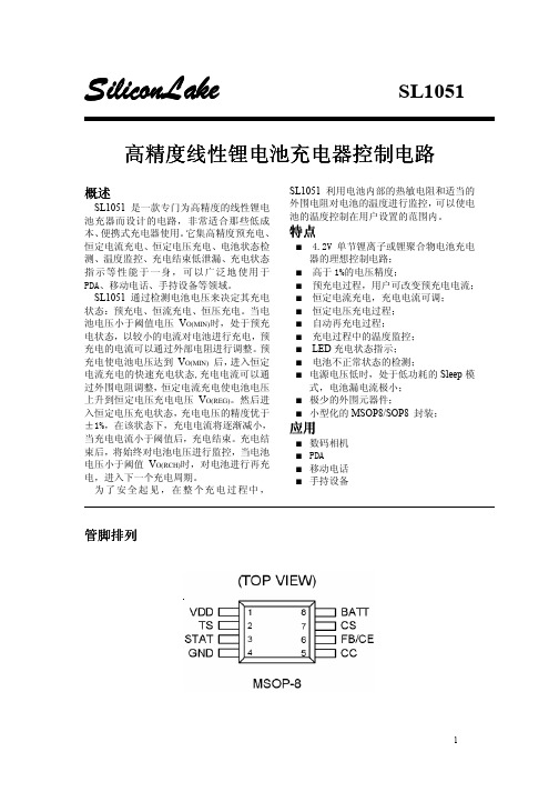
如下:
假设待设定的温度范围为 TL~TH,(其
中 TL<TH);电池中使用的是负温度系数
的热敏电阻(NTC),RTL 为其在温度 TL 时
图6
的阻值,RTH 为其在温度 TH 时的阻值,则 8、充电指示
6
SiliconLake
SL1051
SL1051 的 STAT 有三种状态显示,如下表 所示。
状态 充电
式,电池漏电流极小; ■ 极少的外围元器件; ■ 小型化的 MSOP8/SOP8 封装;
应用
■ 数码相机 ■ PDA ■ 移动电话 ■ 手持设备
管脚排列
1
SiliconLake 引脚描述
SL1051
引脚名称 VDD TS
STAT
GND CC
FB/CE CS BATT
引脚功能 电源端。 温度监控输入端。该引脚的输入电压必须在 VTS1 与 VTS2 之间;否则,将 视为电池温度超出设置范围。 充电状态指示。在充电过程中,该引脚被上拉到高电平;充电结束后,被 下拉到低电平;电池不正常或 TS 温度超过设置的范围时,输出为高阻态。 接地端。 调整管驱动端。与外部调整管的基极(PNP 晶体管)或栅极(PMOS 管) 相连。 外部反馈输入或充电使能控制。 电流采样输入。充电电流通过电源和此引角之间的电压差决定。 电池电压检测输入端。
SiliconLake
SL1051
高精度线性锂电池充电器控制电路
概述
SL1051 是一款专门为高精度的线性锂电 池充器而设计的电路,非常适合那些低成 本、便携式充电器使用。它集高精度预充电、 恒定电流充电、恒定电压充电、电池状态检 测、温度监控、充电结束低泄漏、充电状态 指示等性能于一身,可以广泛地使用于 PDA、移动电话、手持设备等领域。
CY7C64013C-PXC资料
CY7C64013CCY7C64113CFull-Speed USB (12-Mbps) Function Full-Speed USB (12-Mbps) FunctionTABLE OF CONTENTS1.0 FEATURES (6)2.0 FUNCTIONAL OVERVIEW (7)3.0 PIN CONFIGURATIONS (9)4.0 PRODUCT SUMMARY TABLES (10)4.1 Pin Assignments (10)4.2 I/O Register Summary (10)4.3 Instruction Set Summary (12)5.0 PROGRAMMING MODEL (13)5.1 14-Bit Program Counter (PC) (13)5.1.1 Program Memory Organization (14)5.2 8-Bit Accumulator (A) (15)5.3 8-Bit Temporary Register (X) (15)5.4 8-Bit Program Stack Pointer (PSP) (15)5.4.1 Data Memory Organization (15)5.5 8-Bit Data Stack Pointer (DSP) (16)5.6 Address Modes (16)5.6.1 Data (Immediate) (16)5.6.2 Direct (16)5.6.3 Indexed (16)6.0 CLOCKING (17)7.0 RESET (17)7.1 Power-On Reset (POR) (17)7.2 Watchdog Reset (WDR) (17)8.0 SUSPEND MODE (18)9.0 GENERAL-PURPOSE I/O (GPIO) PORTS (19)9.1 GPIO Configuration Port (20)9.2 GPIO Interrupt Enable Ports (21)10.0 DAC PORT (21)10.1 DAC Isink Registers (22)10.2 DAC Port Interrupts (23)11.0 12-BIT FREE-RUNNING TIMER (23)12.0 I2C AND HAPI CONFIGURATION REGISTER (24)13.0 I2C-COMPATIBLE CONTROLLER (25)14.0 HARDWARE ASSISTED PARALLEL INTERFACE (HAPI) (27)15.0 PROCESSOR STATUS AND CONTROL REGISTER (28)16.0 INTERRUPTS (29)16.1 Interrupt Vectors (30)16.2 Interrupt Latency (31)16.3 USB Bus Reset Interrupt (31)16.4 Timer Interrupt (31)16.5 USB Endpoint Interrupts (31)TABLE OF CONTENTS16.6 DAC Interrupt (31)16.7 GPIO/HAPI Interrupt (32)16.8 I2C Interrupt (32)17.0 USB OVERVIEW (33)17.1 USB Serial Interface Engine (SIE) (33)17.2 USB Enumeration (33)17.3 USB Upstream Port Status and Control (33)18.0 USB SERIAL INTERFACE ENGINE OPERATION (34)18.1 USB Device Address (34)18.2 USB Device Endpoints (35)18.3 USB Control Endpoint Mode Register (35)18.4 USB Non-Control Endpoint Mode Registers (36)18.5 USB Endpoint Counter Registers (36)18.6 Endpoint Mode/Count Registers Update and Locking Mechanism (37)19.0 USB MODE TABLES (39)20.0 REGISTER SUMMARY (43)21.0 SAMPLE SCHEMATIC (44)22.0 ABSOLUTE MAXIMUM RATINGS (45)23.0 ELECTRICAL CHARACTERISTICSFOSC = 6 MHZ; OPERATING TEMPERATURE = 0 TO 70°C, V CC = 4.0V TO 5.25V (45)24.0 SWITCHING CHARACTERISTICS (fOSC = 6.0 MHz) (46)25.0 ORDERING INFORMATION (48)26.0 PACKAGE DIAGRAMS (49)LIST OF FIGURESFigure 6-1. Clock Oscillator On-Chip Circuit (17)Figure 7-1. Watchdog Reset (WDR) (18)Figure 9-1. Block Diagram of a GPIO Pin (19)Figure 9-2. Port 0 Data (19)Figure 9-3. Port 1 Data (19)Figure 9-4. Port 2 Data (19)Figure 9-5. Port 3 Data (20)Figure 9-6. GPIO Configuration Register (20)Figure 9-7. Port 0 Interrupt Enable (21)Figure 9-8. Port 1 Interrupt Enable (21)Figure 9-9. Port 2 Interrupt Enable (21)Figure 9-10. Port 3 Interrupt Enable (21)Figure 10-1. Block Diagram of a DAC Pin (22)Figure 10-2. DAC Port Data (22)Figure 10-3. DAC Sink Register (22)Figure 10-4. DAC Port Interrupt Enable (23)Figure 10-5. DAC Port Interrupt Polarity (23)Figure 11-1. Timer LSB Register (23)Figure 11-2. Timer MSB Register (24)Figure 11-3. Timer Block Diagram (24)Figure 12-1. HAPI/I2C Configuration Register (24)Figure 13-1. I2C Data Register (25)Figure 13-2. I2C Status and Control Register (25)Figure 15-1. Processor Status and Control Register (28)Figure 16-1. Global Interrupt Enable Register (29)Figure 16-2. USB Endpoint Interrupt Enable Register (29)Figure 16-3. Interrupt Controller Function Diagram (30)Figure 16-4. GPIO Interrupt Structure (32)Figure 17-1. USB Status and Control Register (34)Figure 18-1. USB Device Address Registers (34)Figure 18-2. USB Device Endpoint Zero Mode Registers (35)Figure 18-3. USB Non-Control Device Endpoint Mode Registers (36)Figure 18-4. USB Endpoint Counter Registers (36)Figure 18-5. Token/Data Packet Flow Diagram (38)Figure 24-1. Clock Timing (47)Figure 24-2. USB Data Signal Timing (47)Figure 24-3. HAPI Read by External Interface from USB Microcontroller (47)Figure 24-4. HAPI Write by External Device to USB Microcontroller (48)LIST OF TABLESTable 4-1. Pin Assignments (10)Table 4-2. I/O Register Summary (10)Table 4-3. Instruction Set Summary (12)Table 9-1. GPIO Port Output Control Truth Table and Interrupt Polarity (20)Table 12-1. HAPI Port Configuration (25)Table 12-2. I2C Port Configuration (25)Table 13-1. I2C Status and Control Register Bit Definitions (26)Table 14-1. Port 2 Pin and HAPI Configuration Bit Definitions (27)Table 16-1. Interrupt Vector Assignments (31)Table 17-1. Control Bit Definition for Upstream Port (34)Table 18-1. Memory Allocation for Endpoints (35)Table 19-1. USB Register Mode Encoding (39)Table 19-2. Details of Modes for Differing Traffic Conditions (see Table 19-1 for the decode legend) (41)1.0 Features•Full-speed USB Microcontroller•8-bit USB Optimized Microcontroller—Harvard architecture—6-MHz external clock source—12-MHz internal CPU clock—48-MHz internal clock•Internal memory—256 bytes of RAM—8 KB of PROM (CY7C64013C, CY7C64113C)•Integrated Master/Slave I2C-compatible Controller (100 kHz) enabled through General-Purpose I/O (GPIO) pins •Hardware Assisted Parallel Interface (HAPI) for data transfer to external devices•I/O ports—Three GPIO ports (Port 0 to 2) capable of sinking 7 mA per pin (typical)—An additional GPIO port (Port 3) capable of sinking 12 mA per pin (typical) for high current requirements: LEDs —Higher current drive achievable by connecting multiple GPIO pins together to drive a common output—Each GPIO port can be configured as inputs with internal pull-ups or open drain outputs or traditional CMOS outputs —A Digital to Analog Conversion (DAC) port with programmable current sink outputs is available on the CY7C64113C devices—Maskable interrupts on all I/O pins•12-bit free-running timer with one microsecond clock ticks•Watchdog Timer (WDT)•Internal Power-On Reset (POR)•USB Specification Compliance—Conforms to USB Specification, Version 1.1—Conforms to USB HID Specification, Version 1.1—Supports up to five user configured endpointsUp to four 8-byte data endpointsUp to two 32-byte data endpoints—Integrated USB transceivers•Improved output drivers to reduce EMI•Operating voltage from 4.0V to 5.5V DC•Operating temperature from 0 to 70 degrees Celsius—CY7C64013C available in 28-pin SOIC and 28-pin PDIP packages—CY7C64113C available in 48-pin SSOP packages•Industry-standard programmer support2.0 Functional OverviewThe CY7C64013C and CY7C64113C are 8-bit One Time Programmable microcontrollers that are designed for full-speed USB applications. The instruction set has been optimized specifically for USB operations, although the microcontrollers can be used for a variety of non-USB embedded applications.GPIOThe CY7C64013C features 19 GPIO pins to support USB and other applications. The I/O pins are grouped into three ports (P0[7:0], P1[2:0], P2[6:2], P3[2:0]) where each port can be configured as inputs with internal pull-ups, open drain outputs, or traditional CMOS outputs. There are 16 GPIO pins (Ports 0 and 1) which are rated at 7 mA typical sink current. Port 3 pins are rated at 12 mA typical sink current, a current sufficient to drive LEDs. Multiple GPIO pins can be connected together to drive a single output for more drive current capacity. Additionally, each GPIO can be used to generate a GPIO interrupt to the microcon-troller. All of the GPIO interrupts share the same “GPIO” interrupt vector.The CY7C64113C has 32 GPIO pins (P0[7:0], P1[7:0], P2[7:0], P3[7:0])DACThe CY7C64113C has four programmable sink current I/O pins (DAC) pins (P4[7,2:0]). Every DAC pin includes an integrated 14-kΩ pull-up resistor. When a ‘1’ is written to a DAC I/O pin, the output current sink is disabled and the output pin is driven HIGH by the internal pull-up resistor. When a ‘0’ is written to a DAC I/O pin, the internal pull-up resistor is disabled and the output pin provides the programmed amount of sink current. A DAC I/O pin can be used as an input with an internal pull-up by writing a ‘1’to the pin.The sink current for each DAC I/O pin can be individually programmed to one of 16 values using dedicated Isink registers. DAC bits P4[1:0] can be used as high-current outputs with a programmable sink current range of 3.2 to 16 mA (typical). DAC bits P4[7,2] have a programmable current sink range of 0.2 to 1.0 mA (typical). Multiple DAC pins can be connected together to drive a single output that requires more sink current capacity. Each I/O pin can be used to generate a DAC interrupt to the microcon-troller. Also, the interrupt polarity for each DAC I/O pin is individually programmable.ClockThe microcontroller uses an external 6-MHz crystal and an internal oscillator to provide a reference to an internal PLL-based clock generator. This technology allows the customer application to use an inexpensive 6-MHz fundamental crystal that reduces the clock-related noise emissions (EMI). A PLL clock generator provides the 6-, 12-, and 48-MHz clock signals for distribution within the microcontroller.MemoryThe CY7C64013C and CY7C64113C have 8 KB of PROM.Power on Reset, Watchdog and Free running TimeThese parts include power-on reset logic, a Watchdog timer, and a 12-bit free-running timer. The power-on reset (POR) logic detects when power is applied to the device, resets the logic to a known state, and begins executing instructions at PROM address 0x0000. The Watchdog timer is used to ensure the microcontroller recovers after a period of inactivity. The firmware may become inactive for a variety of reasons, including errors in the code or a hardware failure such as waiting for an interrupt that never occurs. I2C and HAPI InterfaceThe microcontroller can communicate with external electronics through the GPIO pins. An I2C-compatible interface accommo-dates a 100-kHz serial link with an external device. There is also a Hardware Assisted Parallel Interface (HAPI) which can be used to transfer data to an external device.TimerThe free-running 12-bit timer clocked at 1 MHz provides two interrupt sources, 128-µs and 1.024-ms. The timer can be used to measure the duration of an event under firmware control by reading the timer at the start of the event and after the event is complete. The difference between the two readings indicates the duration of the event in microseconds. The upper four bits of the timer are latched into an internal register when the firmware reads the lower eight bits. A read from the upper four bits actually reads data from the internal register, instead of the timer. This feature eliminates the need for firmware to try to compensate if the upper four bits increment immediately after the lower eight bits are read.InterruptsThe microcontroller supports 11 maskable interrupts in the vectored interrupt controller. Interrupt sources include the USB Bus Reset interrupt, the 128-µs (bit 6) and 1.024-ms (bit 9) outputs from the free-running timer, five USB endpoints, the DAC port, the GPIO ports, and the I2C-compatible master mode interface. The timer bits cause an interrupt (if enabled) when the bit toggles from LOW ‘0’ to HIGH ‘1.’ The USB endpoints interrupt after the USB host has written data to the endpoint FIFO or after the USB controller sends a packet to the USB host. The DAC ports have an additional level of masking that allows the user to select which DAC inputs can cause a DAC interrupt. The GPIO ports also have a level of masking to select which GPIO inputs can cause a GPIO interrupt. For additional flexibility, the input transition polarity that causes an interrupt is programmable for each pin of the DAC port. Input transition polarity can be programmed for each GPIO port as part of the port configuration. The interrupt polarity can be rising edge (‘0’ to ‘1’) or falling edge (‘1’ to ‘0’).Logic Block DiagramInterrupt ControllerPROM 12-bit TimerResetWatchdog TimerPower-On SCLK I 2CGPIO PORT 1GPIO PORT 0P0[7:0]P1[2:0]P1[7:3]SDATA8-b i t B u s6-MHz crystalRAM USB SIE USB TransceiverD+[0]D–[0]Upstream USB PortP3[2:0]DAC PORTDAC[0]DAC[2]High Current OutputsCY7C64113C only256 byte 8 KBClock 6 MHz12-MHz 8-bit CPU*I 2C-compatible interface enabled by firmware through InterfaceP3[7:3]Additional OutputsHigh Current PLL12 MHz48 MHz DividerGPIO/PORT 2P2[0,1,7]P2[3]; Data_Ready P2[4]; STB P2[5]; OE P2[6]; CSP2[2]; Latch_Empty HAPI P2[1:0] or P1[1:0]CY7C64113C onlyPORT 3GPIO DAC[7]3.0Pin Configurations123456791112131415161817XTALIN 108192031302933323534373639384140434245444648472122232425272628V CC P1[1]P1[0]P1[2]P1[4]P1[6]P3[0]P3[2]V REF P1[3]P1[5]P1[7]P3[1]D+[0]D–[0]P3[3]GND P3[5]P3[7]P2[1]P2[3]GND P2[5]P2[7]DAC[7]P0[7]P0[5]P0[3]P0[1]DAC[1]XTALOUT GND P3[4]NC P3[6]P2[0]P2[2]GND P2[4]P2[6]DAC[0]V PP P0[0]P0[2]P0[4]P0[6]DAC[2]CY7C64113C 48-pin SSOPCY7C64013C 1234567911121314XTALIN 1081517161918212023222524262827V CC P1[1]P1[0]P1[2]P3[0]P3[2]GND P2[2]V REF GND P3[1]D+[0]D–[0]P2[3]P2[5]P0[7]P0[5]P0[3]P0[1]P0[6]XTALOUT P2[4]P2[6]V PP P0[0]P0[2]P0[4]28-pin SOICCY7C64013C 28-pin PDIPTOP VIEW1234567911121314XTALIN 1081517161918212023222524262827V CC P1[0]P1[2]P3[0]P3[2]P2[2]GND P2[4]V REF P1[1]GND P3[1]D+[0]D–[0]P2[3]P2[5]P0[7]P0[5]P0[3]P0[1]XTALOUT P2[6]V PP P0[0]P0[2]P0[4]P0[6]4.0Product Summary Tables4.1Pin Assignments4.2I/O Register SummaryI/O registers are accessed via the I/O Read (IORD) and I/O Write (IOWR, IOWX) instructions. IORD reads data from the selected port into the accumulator. IOWR performs the reverse; it writes data from the accumulator to the selected port. Indexed I/O Write (IOWX) adds the contents of X to the address in the instruction to form the port address and writes data from the accumulator to the specified port. Specifying address 0 (e.g., IOWX 0h) means the I/O register is selected solely by the contents of X.All undefined registers are reserved. It is important not to write to reserved registers as this may cause an undefined operation or increased current consumption during operation. When writing to registers with reserved bits, the reserved bits must be written with ‘0.’Table 4-1. Pin Assignments NameI/O 28-Pin SOIC28-Pin PDIP48-Pin SSOPDescriptionD+[0], D–[0]I/O 6, 77, 87, 8Upstream port, USB differential data.P0I/OP0[7:0]10, 14, 11, 15,12, 16, 13, 17P0[7:0]11, 15, 12, 16, 13, 17, 14, 18P0[7:0]20, 26, 21, 27,22, 28, 23, 29GPIO Port 0 capable of sinking 7 mA (typical).P1I/OP1[2:0]25, 27, 26P1[2:0]26, 4, 27P1[7:0]6, 43, 5, 44,4, 45, 47, 46GPIO Port 1 capable of sinking 7 mA (typical).P2I/OP2[6:2]19, 9, 20, 8,21P2[6:2]20, 10, 21,9, 23P2[7:0]18, 32, 17, 33,15, 35, 14, 36GPIO Port 2 capable of sinking 7 mA (typical). HAPI is also supported through P2[6:2].P3I/OP3[2:0]23, 5, 24P3[2:0]24, 6, 25P3[7:0]13, 37, 12, 39,10, 41, 7, 42GPIO Port 3, capable of sinking 12 mA (typical).DAC I/ODAC[7,2:0]19, 25, 24, 31DAC Port with programmable current sink outputs. DAC[1:0] offer a programmable range of 3.2 to 16 mA typical. DAC[7,2] have a programmable sink current range of 0.2 to 1.0 mA typical.XTAL IN IN 2226-MHz crystal or external clock input.XTAL OUT OUT 1116-MHz crystal out.V PP IN 181930Programming voltage supply, tie to ground during normal operation.V CC IN 282848Voltage supply.GND IN 4, 225, 2211, 16, 34, 40Ground.V REF IN333External 3.3V supply voltage for the differential data output buffers and the D+ pull-up.NC38No Connect.Table 4-2. I/O Register SummaryRegister NameI/O AddressRead/WriteFunctionPage Port 0 Data 0x00R/W GPIO Port 0 Data 19Port 1 Data 0x01R/W GPIO Port 1 Data 19Port 2 Data 0x02R/W GPIO Port 2 Data 19Port 3 Data0x03R/W GPIO Port 3 Data20Port 0 Interrupt Enable 0x04W Interrupt Enable for Pins in Port 021Port 1 Interrupt Enable 0x05W Interrupt Enable for Pins in Port 121Port 2 Interrupt Enable 0x06W Interrupt Enable for Pins in Port 221Port 3 Interrupt Enable0x07WInterrupt Enable for Pins in Port 321Table 4-2. I/O Register Summary (continued)Register Name I/O Address Read/Write Function Page GPIO Configuration0x08R/W GPIO Port Configurations20 HAPI and I2C Configuration0x09R/W HAPI Width and I2C Position Configuration24 USB Device Address A0x10R/W USB Device Address A34 EP A0 Counter Register0x11R/W USB Address A, Endpoint 0 Counter 35 EP A0 Mode Register0x12R/W USB Address A, Endpoint 0 Configuration 34 EP A1 Counter Register0x13R/W USB Address A, Endpoint 1 Counter 35 EP A1 Mode Register0x14R/W USB Address A, Endpoint 1 Configuration 35 EP A2 Counter Register0x15R/W USB Address A, Endpoint 2 Counter 35 EP A2 Mode Register0x16R/W USB Address A, Endpoint 2 Configuration 35 USB Status & Control0x1F R/W USB Upstream Port Traffic Status and Control34 Global Interrupt Enable0x20R/W Global Interrupt Enable 29 Endpoint Interrupt Enable0x21R/W USB Endpoint Interrupt Enables29 Timer (LSB)0x24R Lower 8 Bits of Free-running Timer (1 MHz)23 Timer (MSB)0x25R Upper 4 Bits of Free-running Timer 24 WDT Clear0x26W Watchdog Timer Clear18I2C Control & Status0x28R/W I2C Status and Control25I2C Data0x29R/W I2C Data25 DAC Data0x30R/W DAC Data22 DAC Interrupt Enable0x31W Interrupt Enable for each DAC Pin23 DAC Interrupt Polarity0x32W Interrupt Polarity for each DAC Pin23 DAC Isink0x38-0x3F W Input Sink Current Control for each DAC Pin22 Reserved0x40ReservedEP A3 Counter Register0x41R/W USB Address A, Endpoint 3 Counter35 EP A3 Mode Register0x42R/W USB Address A, Endpoint 3 Configuration34 EP A4 Counter Register0x43R/W USB Address A, Endpoint 4 Counter35 EP A4 Mode Register0x44R/W USB Address A, Endpoint 4 Configuration35 Reserved0x48ReservedReserved0x49ReservedReserved0x4A ReservedReserved0x4B ReservedReserved0x4C ReservedReserved0x4D ReservedReserved0x4E ReservedReserved0x4F ReservedReserved0x50ReservedReserved0x51ReservedProcessor Status & Control0xFF R/W Microprocessor Status and Control Register264.3Instruction Set SummaryRefer to the CYASM Assembler User’s Guide for more details.Table 4-3. Instruction Set SummaryMNEMONIC operand opcode cycles MNEMONIC operand opcode cycles HALT 007NOP204 ADD A,expr data014INC A acc214 ADD A,[expr]direct026INC X x224 ADD A,[X+expr]index037INC [expr]direct237 ADC A,expr data044INC [X+expr]index248 ADC A,[expr]direct056DEC A acc254 ADC A,[X+expr]index067DEC X x264 SUB A,expr data074DEC [expr]direct277 SUB A,[expr]direct086DEC [X+expr]index288 SUB A,[X+expr]index097IORD expr address295 SBB A,expr data0A4IOWR expr address2A5 SBB A,[expr]direct0B6POP A2B4 SBB A,[X+expr]index0C7POP X2C4 OR A,expr data0D4PUSH A2D5 OR A,[expr]direct0E6PUSH X2E5 OR A,[X+expr]index0F7SWAP A,X2F5 AND A,expr data104SWAP A,DSP305 AND A,[expr]direct116MOV [expr],A direct315 AND A,[X+expr]index127MOV [X+expr],A index326 XOR A,expr data134OR [expr],A direct337 XOR A,[expr]direct146OR [X+expr],A index348 XOR A,[X+expr]index157AND [expr],A direct357 CMP A,expr data165AND [X+expr],A index368 CMP A,[expr]direct177XOR [expr],A direct377 CMP A,[X+expr]index188XOR [X+expr],A index388 MOV A,expr data194IOWX [X+expr]index396 MOV A,[expr]direct1A5CPL3A4 MOV A,[X+expr]index1B6ASL3B4 MOV X,expr data1C4ASR3C4 MOV X,[expr]direct1D5RLC3D4 reserved1E RRC 3E4 XPAGE1F4RET 3F8 MOV A,X404DI704 MOV X,A414EI724 MOV PSP,A604RETI738 CALL addr50 - 5F10JC addr C0-CF5 JMP addr80-8F5JNC addr D0-DF5 CALL addr90-9F10JACC addr E0-EF7 JZ addr A0-AF5INDEX addr F0-FF14 JNZ addr B0-BF55.0 Programming Model5.114-Bit Program Counter (PC)The 14-bit program counter (PC) allows access to up to 8 KB of PROM available with the CY7C64x13C architecture. The top 32 bytes of the ROM in the 8 Kb part are reserved for testing purposes. The program counter is cleared during reset, such that the first instruction executed after a reset is at address 0x0000h. Typically, this is a jump instruction to a reset handler that initializes the application (see Interrupt Vectors on page 30).The lower eight bits of the program counter are incremented as instructions are loaded and executed. The upper six bits of the program counter are incremented by executing an XPAGE instruction. As a result, the last instruction executed within a 256-byte “page” of sequential code should be an XPAGE instruction. The assembler directive “XPAGEON” causes the assembler to insert XPAGE instructions automatically. Because instructions can be either one or two bytes long, the assembler may occasionally need to insert a NOP followed by an XPAGE to execute correctly.The address of the next instruction to be executed, the carry flag, and the zero flag are saved as two bytes on the program stack during an interrupt acknowledge or a CALL instruction. The program counter, carry flag, and zero flag are restored from the program stack during a RETI instruction. Only the program counter is restored during a RET instruction.The program counter cannot be accessed directly by the firmware. The program stack can be examined by reading SRAM from location 0x00 and up.5.1.1Program Memory Organizationafter reset Address14-bit PC0x0000Program execution begins here after a reset0x0002USB Bus Reset interrupt vector0x0004128-µs timer interrupt vector0x0006 1.024-ms timer interrupt vector0x0008USB address A endpoint 0 interrupt vector0x000A USB address A endpoint 1 interrupt vector0x000C USB address A endpoint 2 interrupt vector0x000E USB address A endpoint 3 interrupt vector0x0010USB address A endpoint 4 interrupt vector0x0012Reserved0x0014DAC interrupt vector0x0016GPIO interrupt vector0x0018I2C interrupt vector0x001A Program Memory begins here0x1FDF8 KB (-32) PROM ends here (CY7C64013C, CY7C64113C)5.28-Bit Accumulator (A)The accumulator is the general-purpose register for the microcontroller.5.38-Bit Temporary Register (X)The “X” register is available to the firmware for temporary storage of intermediate results. The microcontroller can perform indexed operations based on the value in X. Refer to Section 5.6.3 for additional information.5.48-Bit Program Stack Pointer (PSP)During a reset, the program stack pointer (PSP) is set to 0x00 and “grows” upward from this address. The PSP may be set by firmware, using the MOV PSP,A instruction. The PSP supports interrupt service under hardware control and CALL, RET, and RETI instructions under firmware control. The PSP is not readable by the firmware.During an interrupt acknowledge, interrupts are disabled and the 14-bit program counter, carry flag, and zero flag are written as two bytes of data memory. The first byte is stored in the memory addressed by the PSP, then the PSP is incremented. The second byte is stored in memory addressed by the PSP, and the PSP is incremented again. The overall effect is to store the program counter and flags on the program “stack” and increment the PSP by two.The Return from Interrupt (RETI) instruction decrements the PSP, then restores the second byte from memory addressed by the PSP. The PSP is decremented again and the first byte is restored from memory addressed by the PSP. After the program counter and flags have been restored from stack, the interrupts are enabled. The overall effect is to restore the program counter and flags from the program stack, decrement the PSP by two, and reenable interrupts.The Call Subroutine (CALL) instruction stores the program counter and flags on the program stack and increments the PSP by two.The Return from Subroutine (RET) instruction restores the program counter but not the flags from the program stack and decre-ments the PSP by two.5.4.1Data Memory OrganizationThe CY7C64x13C microcontrollers provide 256 bytes of data RAM. Normally, the SRAM is partitioned into four areas: program stack, user variables, data stack, and USB endpoint FIFOs. The following is one example of where the program stack, data stack, and user variables areas could be located.After reset Address8-bit DSP8-bit PSP0x00Program Stack Growth (Move DSP[1])8-bit DSP user selected Data Stack GrowthUser variablesUSB FIFO space for five endpoints[2]0xFFNotes:1.Refer to Section 5.5 for a description of DSP.2.Endpoint sizes are fixed by the Endpoint Size Bit (I/O register 0x1F, Bit 7), see Table 18-1.5.58-Bit Data Stack Pointer (DSP)The data stack pointer (DSP) supports PUSH and POP instructions that use the data stack for temporary storage. A PUSH instruction pre-decrements the DSP, then writes data to the memory location addressed by the DSP. A POP instruction reads data from the memory location addressed by the DSP, then post-increments the DSP.During a reset, the DSP is reset to 0x00. A PUSH instruction when DSP equals 0x00 writes data at the top of the data RAM (address 0xFF). This writes data to the memory area reserved for USB endpoint FIFOs. Therefore, the DSP should be indexed at an appropriate memory location that does not compromise the Program Stack, user-defined memory (variables), or the USB endpoint FIFOs.For USB applications, the firmware should set the DSP to an appropriate location to avoid a memory conflict with RAM dedicated to USB FIFOs. The memory requirements for the USB endpoints are described in Section 18.2. Example assembly instructions to do this with two device addresses (FIFOs begin at 0xD8) are shown below:MOV A,20h; Move 20 hex into Accumulator (must be D8h or less)SWAP A,DSP; swap accumulator value into DSP register5.6Address ModesThe CY7C64013C and CY7C64113C microcontrollers support three addressing modes for instructions that require data operands: data, direct, and indexed.5.6.1Data (Immediate)“Data” address mode refers to a data operand that is actually a constant encoded in the instruction. As an example, consider the instruction that loads A with the constant 0xD8:•MOV A,0D8hThis instruction requires two bytes of code where the first byte identifies the “MOV A” instruction with a data operand as the second byte. The second byte of the instruction is the constant “0xD8.” A constant may be referred to by name if a prior “EQU”statement assigns the constant value to the name. For example, the following code is equivalent to the example shown above:•DSPINIT: EQU 0D8h•MOV A,DSPINIT5.6.2Direct“Direct” address mode is used when the data operand is a variable stored in SRAM. In that case, the one byte address of the variable is encoded in the instruction. As an example, consider an instruction that loads A with the contents of memory address location 0x10:•MOV A,[10h]Normally, variable names are assigned to variable addresses using “EQU” statements to improve the readability of the assembler source code. As an example, the following code is equivalent to the example shown above:•buttons: EQU 10h•MOV A,[buttons]5.6.3Indexed“Indexed” address mode allows the firmware to manipulate arrays of data stored in SRAM. The address of the data operand is the sum of a constant encoded in the instruction and the contents of the “X” register. Normally, the constant is the “base” address of an array of data and the X register contains an index that indicates which element of the array is actually addressed:•array:EQU10h•MOV X,3•MOV A,[X+array]This would have the effect of loading A with the fourth element of the SRAM “array” that begins at address 0x10. The fourth element would be at address 0x13.。
- 1、下载文档前请自行甄别文档内容的完整性,平台不提供额外的编辑、内容补充、找答案等附加服务。
- 2、"仅部分预览"的文档,不可在线预览部分如存在完整性等问题,可反馈申请退款(可完整预览的文档不适用该条件!)。
- 3、如文档侵犯您的权益,请联系客服反馈,我们会尽快为您处理(人工客服工作时间:9:00-18:30)。
PRELIMINARY 8-Mbit (512K x 16) Static RAMCY7C1051DV33Features•High speed —t AA = 10 ns •Low active power—I CC = 110 mA @ 10 ns •Low CMOS standby power —I SB2 = 20 mA •2.0V data retention•Automatic power-down when deselected •TTL-compatible inputs and outputs•Easy memory expansion with CE and OE features•Available in lead-free 48-ball FBGA and 44-pin TSOP II packagesFunctional Description [1]The CY7C1051DV33 is a high-performance CMOS Static RAM organized as 512K words by 16 bits.Write to the device by taking Chip Enable (CE) and Write Enable (WE) inputs LOW. If Byte LOW Enable (BLE) is LOW,then data from IO pins (IO 0–IO 7), is written into the location specified on the address pins (A 0–A 18). If Byte HIGH Enable (BHE) is LOW, then data from IO pins (IO 8–IO 15) is written into the location specified on the address pins (A 0–A 18).Read from the device by taking Chip Enable (CE) and Output Enable (OE) LOW while forcing the Write Enable (WE) HIGH.If Byte LOW Enable (BLE) is LOW, then data from the memory location specified by the address pins will appear on IO 0–IO 7.If Byte HIGH Enable (BHE) is LOW, then data from memory will appear on IO 8 to IO 15. See the “Truth Table” on page 8 for a complete description of Read and Write modes.The input/output pins (IO 0–IO 15) are placed in a high-impedance state when the device is deselected (CE HIGH), the outputs are disabled (OE HIGH), the BHE and BLE are disabled (BHE, BLE HIGH), or a Write operation (CE LOW,and WE LOW) is in progress.The CY7C1051DV33 is available in a 44-pin TSOP II package with center power and ground (revolutionary) pinout, as well as a 48-ball fine-pitch ball grid array (FBGA) package.Note1.For guidelines on SRAM system design, please refer to the “System Design Guidelines” Cypress application note, available on the internet at .1415Logic Block DiagramA 1A 2A 3A 4A 5A 6A 7A 8COLUMN DECODERR O W D E C O D E RS E N S E A M P SINPUT BUFFER512K × 16ARRAYA 0A 11A 13A 12A A A 16A 17A 18A 9A 10IO 0–IO 7OE IO 8–IO 15CE WE BLEBHEPRELIMINARY CY7C1051DV33Selection Guide–10Unit Maximum Access Time 10ns Maximum Operating Current 110mA Maximum CMOS Standby Current20mAPin Configurations [2]48-ball Mini FBGAWE V CC A 11A 10NC A 6A 0A 3CE IO 10IO 8IO 9A 4A 5IO 11IO 13IO 12IO 14IO 15V SS A 9A 8OE V SS A 7IO 0BHE NC A 17A 2A 1BLE V CC IO 2IO 1IO 3IO 4IO 5IO 6IO 7A 15A 14A 13A 12NC A 18NC326541D E B A C F G HA 16(Top View)TSOP IIWE 1234567891011143132363534333740393812134144434216152930V CC A 5A 6A 7A 8A 0A 1OE V SS A 17IO 15A 2CE IO 2IO 0IO 1BHE A 3A 418172019IO 32728252622212324V SS IO 6IO 4IO 5IO 7A 16A 15BLE V CC IO 14IO 13IO 12IO 11IO 10IO 9IO 8A 14A 13A 12A 11A 9A 10A 18(Top View)Note2.NC pins are not connected on the diePRELIMINARY CY7C1051DV33Maximum Ratings(Exceeding the maximum ratings may impair the useful life of the device. These are for user guidelines, they are not tested.)Storage Temperature .................................–65°C to +150°C Ambient Temperature withPower Applied.............................................–55°C to +125°C Supply Voltage on V CC to Relative GND [3]....–0.5V to +4.6V DC Voltage Applied to Outputsin High-Z State [3]....................................–0.3V to V CC + 0.3V DC Input Voltage [3].................................–0.3V to V CC + 0.3VCurrent into Outputs (LOW).........................................20 mA Static Discharge Voltage............................................>2001V (per MIL-STD-883, Method 3015)Latch-up Current......................................................>200 mAOperating RangeRange Ambient Temperature V CC Industrial–40°C to +85°C3.3V ± 0.3VDC Electrical Characteristics Over the Operating RangeParameter DescriptionTest Conditions–10Unit Min MaxV OH Output HIGH Voltage V CC = Min, I OH = –4.0 mA 2.4V V OL Output LOW Voltage V CC = Min, I OL = 8.0 mA0.4V V IH Input HIGH Voltage 2.0V CC + 0.3V V IL [3]Input LOW Voltage –0.30.8V I IX Input Leakage Current GND < V I < V CC–1+1μA I OZ Output Leakage Current GND < V OUT < V CC , Output Disabled –1+1μA I CCV CC Operating Supply CurrentV CC = Max, f = f MAX = 1/t RC100 MHz 110mA83 MHz 100 66 MHz 9040 MHz80I SB1Automatic CE Power Down Current —TTL Inputs Max V CC , CE > V IH V IN > V IH or V IN < V IL , f = f MAX 40mA I SB2Automatic CE Power Down Current —CMOS Inputs Max V CC , CE > V CC – 0.3V,V IN > V CC – 0.3V or V IN < 0.3V, f = 020mACapacitance [4]Parameter DescriptionTest ConditionsMax.Unit C IN Input Capacitance T A = 25°C, f = 1 MHz, V CC = 3.3V12pF C OUTIO Capacitance12pFNotes3.V IL (min) = –2.0V and V IH (max) = V CC + 2.0V for pulse durations of less than 20 ns.4.Tested initially and after any design or process changes that may affect these parametersThermal Resistance [4]ParameterDescription Test ConditionsFBGA PackageTSOP II PackageUnit ΘJA Thermal Resistance (Junction to Ambient)Still Air, soldered on a 3 × 4.5 inch, four-layer printed circuit board28.3151.43°C/W ΘJCThermal Resistance (Junction to Case)11.415.8°C/WPRELIMINARYCY7C1051DV33AC Test Loads and Waveforms [5]AC Switching Characteristics [6] Over the Operating RangeParameterDescription–10UnitMinMaxRead Cycle t power [7]V CC (typical) to the first access 100μs t RC Read Cycle Time 10ns t AA Address to Data Valid10ns t OHA Data Hold from Address Change 3ns t ACE CE LOW to Data Valid 10ns t DOE OE LOW to Data Valid 5ns t LZOE OE LOW to Low-Z 0ns t HZOE OE HIGH to High-Z [8, 9]5ns t LZCE CE LOW to Low-Z [9]3ns t HZCE CE HIGH to High-Z [8, 9]5ns t PU CE LOW to Power Up 0ns t PD CE HIGH to Power Down 10ns t DBE Byte Enable to Data Valid 5ns t LZBE Byte Enable to Low-Z 0ns t HZBEByte Disable to High-Z6nsNotes5.AC characteristics (except High-Z) are tested using the load conditions shown in Figure (a). High-Z characteristics are tested for all speeds using the test loadshown in Figure (c).6.Test conditions assume signal transition time of 3 ns or less, timing reference levels of 1.5V, input pulse levels of 0 to 3.0V.7.t POWER gives the minimum amount of time that the power supply should be at typical V CC values until the first memory access can be performed.8.t HZOE , t HZCE , t HZBE and t HZWE are specified with a load capacitance of 5 pF as in part (d) of AC Test Loads.Transition is measured when the outputs enter ahigh impedance state.9.At any given temperature and voltage condition, t HZCE is less than t LZCE , t HZOE is less than t LZOE , t HZBE is less than t LZBE , and t HZWE is less than t LZWE for anygiven device.90%10%3.0VGND90%10%ALL INPUT PULSES * CAPACITIVE LOAD CONSISTS OF ALL COMPONENTS OF THE TEST ENVIRONMENTRise Time: 1 V/nsFall Time: 1 V/ns30 pF*OUTPUTZ = 50Ω50Ω1.5V (a)3.3V OUTPUT5 pF(c)R 317ΩR2351ΩHigh-Z Characteristics(b)PRELIMINARY CY7C1051DV33Data Retention WaveformWrite Cycle [10, 11]t WC Write Cycle Time 10ns t SCE CE LOW to Write End 7ns t AW Address Setup to Write End 7ns t HA Address Hold from Write End 0ns t SA Address Setup to Write Start 0ns t PWE WE Pulse Width 7ns t SD Data Setup to Write End 5ns t HD Data Hold from Write End 0ns t LZWE WE HIGH to Low-Z [9]3ns t HZWE WE LOW to High-Z [8, 9]5ns t BWByte Enable to End of Write7nsData Retention Characteristics Over the Operating RangeParameter DescriptionConditions [12]Min MaxUnit V DR V CC for Data Retention 2.0V I CCDR Data Retention CurrentV CC = V DR = 2.0V , CE > V CC – 0.3V , V IN > V CC – 0.3V or V IN < 0.3V20mA t CDR [4]Chip Deselect to Data Retention Time 0ns t R [13]Operation Recovery Timet RCnsAC Switching Characteristics [6] Over the Operating Range (continued)ParameterDescription–10UnitMinMax3.0V 3.0V t CDRV DR > 2VDATA RETENTION MODEt RCEV CC Notes10.The internal Write time of the memory is defined by the overlap of CE LOW, and WE LOW. CE and WE must be LOW to initiate a Write, and the transition ofeither of these signals can terminate the Write. The input data setup and hold timing should be referenced to the leading edge of the signal that terminates the Write.11.The minimum Write cycle time for Write Cycle No. 3 (WE controlled, OE LOW) is the sum of t HZWE and t SD .12.No inputs may exceed V CC + 0.3V13.Full device operation requires linear V CC ramp from V DR to V CC (min) > 50 μs or stable at V CC (min) > 50 μs.PRELIMINARY CY7C1051DV33Switching WaveformsRead Cycle No. 1[14, 15]Read Cycle No. 2 (OE Controlled)[15, 16]Notes14.Device is continuously selected. OE, CE, BHE or BHE or both= V IL .15.WE is HIGH for Read cycle.16.Address valid prior to or coincident with CE transition LOW.PREVIOUS DATA VALIDDATA VALIDt RCt AAt OHAADDRESSDATA OUT50%50%DATA VALIDt RCt ACEt DOE t LZOE t LZCE t PUHIGH IMPEDANCEt HZOEt HZBEt PDHIGHOE CEICC ISB IMPEDANCEADDRESSDATA OUT V CC SUPPLY t DBE t LZBEt HZCE BHE,BLECURRENTI CCI SBPRELIMINARY CY7C1051DV33Write Cycle No. 1 (CE Controlled)[17, 18]Write Cycle No. 2 (BLE or BHE Controlled)Notes17.Data I/O is high-impedance if OE or BHE or BLE or both = V IH .18.If CE goes HIGH simultaneously with WE going HIGH, the output remains in a high-impedance state.Switching Waveforms (continued)t HDt SDt SCEt SA t HAt AWt PWEt WCBWDATAI/OADDRESSCEWEBHE,BLEt t HDt SDt BWt SA t HAt AWt PWEt WCt SCEDATAI/OADDRESSBHE,BLEWECEPRELIMINARY CY7C1051DV33Write Cycle No. 3 (WE Controlled, OE LOW)Switching Waveforms (continued)t HDt SDt SCEt HAt AWt PWEt WCt BWDATA I/OADDRESSCEWEBHE,BLEt SAt LZWEt HZWETruth TableCE OE WE BLE BHE I/O 0–I/O 7I/O 8–I/O 15ModePower H X X X X High-Z High-Z Power-down Standby (I SB )L L H L L Data Out Data Out Read All Bits Active (I CC )L L H L H Data Out High-Z Read Lower Bits Only Active (I CC )L L H H L High-Z Data Out Read Upper Bits Only Active (I CC )L X L L L Data In Data In Write All Bits Active (I CC )L X L L H Data In High-Z Write Lower Bits Only Active (I CC )L X L H L High-Z Data In Write Upper Bits Only Active (I CC )LHHXXHigh-ZHigh-ZSelected, Outputs DisabledActive (I CC )Ordering InformationSpeed (ns)Ordering Code Package Diagram Package TypeOperating Range 10CY7C1051DV33-10BAXI 51-8510648-ball FBGA (Pb-Free)IndustrialCY7C1051DV33-10ZSXI51-8508744-pin TSOP II (Pb-Free)Please contact your local Cypress sales representative for availability of these parts.PRELIMINARY CY7C1051DV33 Package DiagramsPRELIMINARY CY7C1051DV33Document #: 001-00063 Rev. *C Page 10 of 11© Cypress Semiconductor Corporation, 2006-2007. The information contained herein is subject to change without notice. Cypress Semiconductor Corporation assumes no responsibility for the All products and company names mentioned in this document may be the trademarks of their respective holders.Figure 2. 44-pin TSOP II (51-85087)Package Diagrams (continued)51-85087-*APRELIMINARY CY7C1051DV33Document #: 001-00063 Rev. *C Page 11 of 11Document History Page Document Title: CY7C1051DV33 8-Mbit (512K x 16) Static RAM Document Number: 001-00063REV.ECN NO.Issue Date Orig. of Change Description of Change **342195See ECN PCI New Data Sheet *A 380574See ECN SYT Redefined I CC values for Com’l and Ind’l temperature rangesI CC (Com’l): Changed from 110, 90 and 80 mA to 110, 100 and 95 mA for 8, 10and 12 ns speed bins respectivelyI CC (Ind’l): Changed from 110, 90 and 80 mA to 120, 110 and 105 mA for 8, 10and 12 ns speed bins respectivelyChanged the Capacitance values from 8 pF to 10 pF on Page # 3*B 485796See ECN NXR Changed address of Cypress Semiconductor Corporation on Page# 1 from“3901 North First Street” to “198 Champion Court”Removed -8 and -12 Speed bins from product offering,Removed Commercial Operating Range option,Modified Maximum Ratings for DC input voltage from -0.5V to -0.3V andV CC + 0.5V to V CC + 0.3VChanged the Description of I IX from Input Load Current toInput Leakage Current.Changed t HZBE from 5 ns to 6 nsUpdated footnote #7 on High-Z parameter measurementAdded footnote #11Updated the Ordering Information table and Replaced Package Name columnwith Package Diagram.*C 866000See ECN NXRChanged ball E3 from V SS to NC in FBGA pin configuration [+] FeedbThis datasheet has been downloaded from:Free DownloadDaily Updated Database100% Free Datasheet Search Site100% Free IC Replacement Search SiteConvenient Electronic DictionaryFast Search SystemAll Datasheets Cannot Be Modified Without PermissionCopyright © Each Manufacturing Company。