《半导体芯片制造技术》课件(7)
半导体芯片制造技术
⑸固定的熔点
图1-8 晶体非晶体的加热曲线
2. 晶体的缺陷 晶体缺陷按缺陷的几何尺寸可分为点缺陷,如空 位、间隙原子;线缺陷,如位错;及面缺陷,如晶粒 间界和堆垛层错等。
第三节 半导体生产污染控制
一、污染物种类
1.颗粒污染物 颗粒包括空气中所含的颗粒、人员产生的颗粒、 设备和工艺操作过程中使用的化学品产生的颗粒等。 在任何晶片上,都存在大量的颗粒。有些位于器件不 太敏感的区域,不会造成器件缺陷,而有些则属于致 命性的。根据经验得出的法则是:颗粒的大小要小于 器件上最小的特征图形尺寸的1/10,否则,就会形成 缺陷。
单晶体
多晶体
非晶体
图1-3 特性, 称之为晶体的自限性。
⑶各向异性 晶体的物理性质随着晶面的方向不同而不同, 称为晶体的各向异性。
图1-7 云母片和玻璃片的石蜡熔化实验
⑷对称性 晶体在某几个特定的方向上所表现出的物理、 化学性质完全相同。在晶体中,如果沿某些特定的 方向原子排列的密度相同,则沿这些方向的性能相 同。
浓度/(粒/ 升) 小于等于1 小于等于10
最高 最低 最高 最低
噪声(A声 级)/db
100
1000 10000
大于等 于0.5
小于等于 100
小于等于 1000
27
18
60
40
小于等于70
小于等于 10000
五、洁净室的维护 超净间的定期维护是非常必要的。清洁人员 必须要穿着与生产人员一样的洁净服,超净 间的清洁器具,包括拖把,也要仔细选择。 一般家庭使用的清洁器具太脏,无法在超净 间使用。而且使用真空吸尘器也要特别注意。 真空吸尘器中的排风系统中,装有HEPA过 滤器,现在已经可以在超净间中使用。许多 超净间采用内置式真空系统来减少清洁时产 生的脏东西。
芯片制造-半导体工艺与设备教学课件完整版
1.5 半导体工业的构成
• 半导体工业包括材料供应、电路设计、芯片制造和半导体 工业设备及化学品供应五大块。
• 目前有三类企业:一种是集设计、制造、封装和市场销售 为一体的公司;另一类是做设计和销售的公司,他们是从 芯片生产厂家购买芯片;还有一种是芯片生产工厂,他们 可以为顾客生产多种类型的芯片。
第四章 芯片制造
概述: 芯片生产工艺主要有4种最基本的平面制造工艺,分别
是:薄膜制备工艺、光刻与刻蚀工艺、掺杂工艺、热处理 工艺
4.1薄膜制备
淀积
钝化层
是在晶体表面形成薄膜的
加工工艺。右图是MOS晶体管的
淀积 金属膜
剖面图,可以看出上面有钝化
层(Si3N4、Al2O3)、金属膜(Al)、氧生化长层
下卡盘
3.3 晶体外延生长技术
外延是一种采取化学反应法进行晶体生长的另一种技术。 在一定条件下,以衬底晶片作为晶体籽晶,让原子(如硅原 子)有规则地排列在单晶衬底上,形成一层具有一定导电类 型、电阻率、厚度及完整晶格结构的单晶层,由于这个新的 单晶层是在原来衬底晶面向外延伸的结果,所以称其为外延 生长,这个新生长的单晶层叫外延层。最常见的外延生长技 术为化学气相淀积(CVD)和分子束外延生长(MBE)。
封装 良品芯片
被封装 并测试
良品
3 晶圆制备
概述: 高密度和大尺寸芯片的发展需要大直径的晶圆,
最早使用的是1英寸(25mm),而现在12英寸(300mm) 直径的晶圆已经投入生产线了。因为晶圆直径越大, 单个芯片的生产成本就越低。然而,直径越大,晶体 结构上和电学性能的一致性就越难以保证,这正是对 晶圆生产的一个挑战。
• 外延生长的基本原理
氢还原四氯化硅外延生长原理示意图
半导体制造技术第十四章PPT课件

光学增强技术
• 相移掩膜技术 • 光学临近修正 • 离轴照明
对准
• 对准就是确定硅片上图形的位置、方向和图形转 换的过程。
• 对准过程的结果,或者每个连续的图形与先前层 匹配的精度,被称做套准。
• 套准精度是测量对准系统把版图套准到硅片上图 形的能力。套准容差描述要形成的图形层和前层 的最大相对位移。一般套准容差是关键尺寸的三 分之一。
环境条件
• 温度 • 湿度 • 振动 • 大气压力 • 颗粒沾污
对准和曝光的质量测量
• 聚焦-曝光剂量 • 光强 • 掩膜板对准 • 图形分辨率 • 投影掩膜板的质量
写在最后
经常不断地学习,你就什么都知道。你知道得越多,你就越有力量 Study Constantly, And You Will Know Everything. The More
You Know, The More Powerful You Will Be
谢大家
荣幸这一路,与你同行
It'S An Honor To Walk With You All The Way
演讲人:XXXXXX 时 间:XX年XX月XX日
• 可以通过增加镜头半径来增加数值孔径并俘获更 多的衍射光,但是这样的光学系统更加复杂更加 昂贵。
抗反射涂层使用的原因
• 光刻胶的下面是最终要被刻蚀形成图案的底层薄 膜。如果这个底层是反光的,那么光线将从这个 膜层反射并有可能损害临近的光刻胶。这个损害 能够对线宽控制产生不利的影响。
• 两种最主要的光反射问题是反射切口和驻波。
分辨率
• 光刻中,分辨率被定义为清晰分辨出硅片上间隔 很近的特征图形对的能力。分辨率对于任何光学 系统都是一个重要的参数。
半导体制造技术
Semiconductor Manufacturing Technology半导体制造技术Instructor’s ManualMichael QuirkJulian SerdaCopyright Prentice HallTable of Contents目录OverviewI. Chapter1. Semiconductor industry overview2. Semiconductor materials3. Device technologies—IC families4. Silicon and wafer preparation5. Chemicals in the industry6. Contamination control7. Process metrology8. Process gas controls9. IC fabrication overview10. Oxidation11. Deposition12. Metallization13. Photoresist14. Exposure15. Develop16. Etch17. Ion implant18. Polish19. Test20. Assembly and packagingII. Answers to End-of-Chapter Review QuestionsIII. Test Bank (supplied on diskette)IV. Chapter illustrations, tables, bulleted lists and major topics (supplied on CD-ROM)Notes to Instructors:1)The chapter overview provides a concise summary of the main topics in each chapter.2)The correct answer for each test bank question is highlighted in bold. Test bankquestions are based on the end-of-chapter questions. If a student studies the end-of-chapter questions (which are linked to the italicized words in each chapter), then they will be successful on the test bank questions.2Chapter 1Introduction to the Semiconductor Industry Die:管芯 defective:有缺陷的Development of an Industry•The roots of the electronic industry are based on the vacuum tube and early use of silicon for signal transmission prior to World War II. The first electronic computer, the ENIAC, wasdeveloped at the University of Pennsylvania during World War II.•William Shockley, John Bardeen and Walter Brattain invented the solid-state transistor at Bell Telephone Laboratories on December 16, 1947. The semiconductor industry grew rapidly in the 1950s to commercialize the new transistor technology, with many early pioneers working inSilicon Valley in Northern California.Circuit Integration•The first integrated circuit, or IC, was independently co-invented by Jack Kilby at Texas Instruments and Robert Noyce at Fairchild Semiconductor in 1959. An IC integrates multiple electronic components on one substrate of silicon.•Circuit integration eras are: small scale integration (SSI) with 2 - 50 components, medium scale integration (MSI) with 50 – 5k components, large scale integration (LSI) with 5k to 100kcomponents, very large scale integration (VLSI) with 100k to 1M components, and ultra large scale integration (ULSI) with > 1M components.1IC Fabrication•Chips (or die) are fabricated on a thin slice of silicon, known as a wafer (or substrate). Wafers are fabricated in a facility known as a wafer fab, or simply fab.•The five stages of IC fabrication are:Wafer preparation: silicon is purified and prepared into wafers.Wafer fabrication: microchips are fabricated in a wafer fab by either a merchant chip supplier, captive chip producer, fabless company or foundry.Wafer test: Each individual die is probed and electrically tested to sort for good or bad chips.Assembly and packaging: Each individual die is assembled into its electronic package.Final test: Each packaged IC undergoes final electrical test.•Key semiconductor trends are:Increase in chip performance through reduced critical dimensions (CD), more components per chip (Moore’s law, which predicts the doubling of components every 18-24 months) andreduced power consumption.Increase in chip reliability during usage.Reduction in chip price, with an estimated price reduction of 100 million times for the 50 years prior to 1996.The Electronic Era•The 1950s saw the development of many different types of transistor technology, and lead to the development of the silicon age.•The 1960s were an era of process development to begin the integration of ICs, with many new chip-manufacturing companies.•The 1970s were the era of medium-scale integration and saw increased competition in the industry, the development of the microprocessor and the development of equipment technology. •The 1980s introduced automation into the wafer fab and improvements in manufacturing efficiency and product quality.•The 1990s were the ULSI integration era with the volume production of a wide range of ICs with sub-micron geometries.Career paths•There are a wide range of career paths in semiconductor manufacturing, including technician, engineer and management.2Chapter 2 Characteristics of Semiconductor MaterialsAtomic Structure•The atomic model has three types of particles: neutral neutrons(不带电的中子), positively charged protons(带正电的质子)in the nucleus and negatively charged electrons(带负电的核外电子) that orbit the nucleus. Outermost electrons are in the valence shell, and influence the chemical and physical properties of the atom. Ions form when an atom gains or loses one or more electrons.The Periodic Table•The periodic table lists all known elements. The group number of the periodic table represents the number of valence shell electrons of the element. We are primarily concerned with group numbers IA through VIIIA.•Ionic bonds are formed when valence shell electrons are transferred from the atoms of one element to another. Unstable atoms (e.g., group VIIIA atoms because they lack one electron) easily form ionic bonds.•Covalent bonds have atoms of different elements that share valence shell electrons.3Classifying Materials•There are three difference classes of materials:ConductorsInsulatorsSemiconductors•Conductor materials have low resistance to current flow, such as copper. Insulators have high resistance to current flow. Capacitance is the storage of electrical charge on two conductive plates separated by a dielectric material. The quality of the insulation material between the plates is the dielectric constant. Semiconductor materials can function as either a conductor or insulator.Silicon•Silicon is an elemental semiconductor material because of four valence shell electrons. It occurs in nature as silica and is refined and purified to make wafers.•Pure silicon is intrinsic silicon. The silicon atoms bond together in covalent bonds, which defines many of silicon’s properties. Silicon atoms bond together in set, repeatable patterns, referred to asa crystal.•Germanium was the first semiconductor material used to make chips, but it was soon replaced by silicon. The reasons for this change are:Abundance of siliconHigher melting temperature for wider processing rangeWide temperature range during semiconductor usageNatural growth of silicon dioxide•Silicon dioxide (SiO2) is a high quality, stable electrical insulator material that also serves as a good chemical barrier to protect silicon from external contaminants. The ability to grow stable, thin SiO2 is fundamental to the fabrication of Metal-Oxide-Semiconductor (MOS) devices. •Doping increases silicon conductivity by adding small amounts of other elements. Common dopant elements are from trivalent, p-type Group IIIA (boron) and pentavalent, n-type Group VA (phosphorus, arsenic and antimony).•It is the junction between the n-type and p-type doped regions (referred to as a pn junction) that permit silicon to function as a semiconductor.4Alternative Semiconductor Materials•The alternative semiconductor materials are primarily the compound semiconductors. They are formed from Group IIIA and Group VA (referred to as III-V compounds). An example is gallium arsenide (GaAs).•Some alternative semiconductors come from Group IIA and VIA, referred to as II-VI compounds. •GaAs is the most common III-V compound semiconductor material. GaAs ICs have greater electron mobility, and therefore are faster than ICs made with silicon. GaAs ICs also have higher radiation hardness than silicon, which is better for space and military applications. The primary disadvantage of GaAs is the lack of a natural oxide.5Chapter 3Device TechnologiesCircuit Types•There are two basic types of circuits: analog and digital. Analog circuits have electrical data that varies continuously over a range of voltage, current and power values. Digital circuits have operating signals that vary about two distinct voltage levels – a high and a low.Passive Component Structures•Passive components such as resistors and capacitors conduct electrical current regardless of how the component is connected. IC resistors are a passive component. They can have unwanted resistance known as parasitic resistance. IC capacitor structures can also have unintentional capacitanceActive Component Structures•Active components, such as diodes and transistors can be used to control the direction of current flow. PN junction diodes are formed when there is a region of n-type semiconductor adjacent to a region of p-type semiconductor. A difference in charge at the pn junction creates a depletion region that results in a barrier voltage that must be overcome before a diode can be operated. A bias voltage can be configured to have a reverse bias, with little or no conduction through the diode, or with a forward bias, which permits current flow.•The bipolar junction transistor (BJT) has three electrodes and two pn junctions. A BJT is configured as an npn or pnp transistor and biased for conduction mode. It is a current-amplifying device.6• A schottky diode is formed when metal is brought in contact with a lightly doped n-type semiconductor material. This diode is used in faster and more power efficient BJT circuits.•The field-effect transistor (FET), a voltage-amplifying device, is more compact and power efficient than BJT devices. A thin gate oxide located between the other two electrodes of the transistor insulates the gate on the MOSFET. There are two categories of MOSFETs, nMOS (n-channel) and pMOS (p-channel), each which is defined by its majority current carriers. There is a biasing scheme for operating each type of MOSFET in conduction mode.•For many years, nMOS transistors have been the choice of most IC manufacturers. CMOS, with both nMOS and pMOS transistors in the same IC, has been the most popular device technology since the early 1980s.•BiCMOS technology makes use of the best features of both CMOS and bipolar technology in the same IC device.•Another way to categorize FETs is in terms of enhancement mode and depletion mode. The major different is in the way the channels are doped: enhancement-mode channels are doped opposite in polarity to the source and drain regions, whereas depletion mode channels are doped the same as their respective source and drain regions.Latchup in CMOS Devices•Parasitic transistors can create a latchup condition(???????) in CMOS ICs that causes transistors to unintentionally(无心的) turn on. To control latchup, an epitaxial layer is grown on the wafer surface and an isolation barrier(隔离阻障)is placed between the transistors. An isolation layer can also be buried deep below the transistors.Integrated Circuit Productsz There are a wide range of semiconductor ICs found in electrical and electronic products. This includes the linear IC family, which operates primarily with anal3og circuit applications, and the digital IC family, which includes devices that operate with binary bits of data signals.7Chapter 4Silicon and Wafer Preparation8z Semiconductor-Grade Silicon•The highly refined silicon used for wafer fabrication is termed semiconductor-grade silicon (SGS), and sometimes referred to as electronic-grade silicon. The ultra-high purity of semiconductor-grade silicon is obtained from a multi-step process referred to as the Siemens process.Crystal Structure• A crystal is a solid material with an ordered, 3-dimensional pattern over a long range. This is different from an amorphous material that lacks a repetitive structure.•The unit cell is the most fundamental entity for the long-range order found in crystals. The silicon unit cell is a face-centered cubic diamond structure. Unit cells can be organized in a non-regular arrangement, known as a polycrystal. A monocrystal are neatly arranged unit cells.Crystal Orientation•The orientation of unit cells in a crystal is described by a set of numbers known as Miller indices.The most common crystal planes on a wafer are (100), (110), and (111). Wafers with a (100) crystal plane orientation are most common for MOS devices, whereas (111) is most common for bipolar devices.Monocrystal Silicon Growth•Silicon monocrystal ingots are grown with the Czochralski (CZ) method to achieve the correct crystal orientation and doping. A CZ crystal puller is used to grow the silicon ingots. Chunks of silicon are heated in a crucible in the furnace of the puller, while a perfect silicon crystal seed is used to start the new crystal structure.• A pull process serves to precisely replicate the seed structure. The main parameters during the ingot growth are pull rate and crystal rotation. More homogeneous crystals are achieved with a magnetic field around the silicon melt, known as magnetic CZ.•Dopant material is added to the melt to dope the silicon ingot to the desired electrical resistivity.Impurities are controlled during ingot growth. A float-zone crystal growth method is used toachieve high-purity silicon with lower oxygen content.•Large-diameter ingots are grown today, with a transition underway to produce 300-mm ingot diameters. There are cost benefits for larger diameter wafers, including more die produced on a single wafer.Crystal Defects in Silicon•Crystal defects are interruptions in the repetitive nature of the unit cell. Defect density is the number of defects per square centimeter of wafer surface.•Three general types of crystal defects are: 1) point defects, 2) dislocations, and 3) gross defects.Point defects are vacancies (or voids), interstitial (an atom located in a void) and Frenkel defects, where an atom leaves its lattice site and positions itself in a void. A form of dislocation is astacking fault, which is due to layer stacking errors. Oxygen-induced stacking faults are induced following thermal oxidation. Gross defects are related to the crystal structure (often occurring during crystal growth).Wafer Preparation•The cylindrical, single-crystal ingot undergoes a series of process steps to create wafers, including machining operations, chemical operations, surface polishing and quality checks.•The first wafer preparation steps are the shaping operations: end removal, diameter grinding, and wafer flat or notch. Once these are complete, the ingot undergoes wafer slicing, followed by wafer lapping to remove mechanical damage and an edge contour. Wafer etching is done to chemically remove damage and contamination, followed by polishing. The final steps are cleaning, wafer evaluation and packaging.Quality Measures•Wafer suppliers must produce wafers to stringent quality requirements, including: Physical dimensions: actual dimensions of the wafer (e.g., thickness, etc.).Flatness: linear thickness variation across the wafer.Microroughness: peaks and valleys found on the wafer surface.Oxygen content: excessive oxygen can affect mechanical and electrical properties.Crystal defects: must be minimized for optimum wafer quality.Particles: controlled to minimize yield loss during wafer fabrication.Bulk resistivity(电阻系数): uniform resistivity from doping during crystal growth is critical. Epitaxial Layer•An epitaxial layer (or epi layer) is grown on the wafer surface to achieve the same single crystal structure of the wafer with control over doping type of the epi layer. Epitaxy minimizes latch-up problems as device geometries continue to shrink.Chapter 5Chemicals in Semiconductor FabricationEquipment Service Chase Production BayChemical Supply Room Chemical Distribution Center Holding tank Chemical drumsProcess equipmentControl unit Pump Filter Raised and perforated floorElectronic control cablesSupply air ductDual-wall piping for leak confinement PumpFilterChemical control and leak detection Valve boxes for leak containment Exhaust air ductStates of Matter• Matter in the universe exists in 3 basic states (宇宙万物存在着三种基本形态): solid, liquid andgas. A fourth state is plasma.Properties of Materials• Material properties are the physical and chemical characteristics that describe its unique identity.• Different properties for chemicals in semiconductor manufacturing are: temperature, pressure andvacuum, condensation, vapor pressure, sublimation and deposition, density, surface tension, thermal expansion and stress.Temperature is a measure of how hot or cold a substance is relative to another substance. Pressure is the force exerted per unit area. Vacuum is the removal of gas molecules.Condensation is the process of changing a gas into a liquid. Vaporization is changing a liquidinto a gas.Vapor pressure is the pressure exerted by a vapor in a closed container at equilibrium.Sublimation is the process of changing a solid directly into a gas. Deposition is changing a gas into a solid.Density is the mass of a substance divided by its volume.Surface tension of a liquid is the energy required to increase the surface area of contact.Thermal expansion is the increase in an object’s dimension due to heating.Stress occurs when an object is exposed to a force.Process Chemicals•Semiconductor manufacturing requires extensive chemicals.• A chemical solution is a chemical mixture. The solvent is the component of the solution present in larger amount. The dissolved substances are the solutes.•Acids are solutions that contain hydrogen and dissociate in water to yield hydronium ions. A base is a substance that contains the OH chemical group and dissociates in water to yield the hydroxide ion, OH-.•The pH scale is used to assess the strength of a solution as an acid or base. The pH scale varies from 0 to 14, with 7 being the neutral point. Acids have pH below 7 and bases have pH values above 7.• A solvent is a substance capable of dissolving another substance to form a solution.• A bulk chemical distribution (BCD) system is often used to deliver liquid chemicals to the process tools. Some chemicals are not suitable for BCD and instead use point-of-use (POU) delivery, which means they are stored and used at the process station.•Gases are generally categorized as bulk gases or specialty gases. Bulk gases are the relatively simple gases to manufacture and are traditionally oxygen, nitrogen, hydrogen, helium and argon.The specialty gases, or process gases, are other important gases used in a wafer fab, and usually supplied in low volume.•Specialty gases are usually transported to the fab in metal cylinders.•The local gas distribution system requires a gas purge to flush out undesirable residual gas. Gas delivery systems have special piping and connections systems. A gas stick controls the incoming gas at the process tool.•Specialty gases may be classified as hydrides, fluorinated compounds or acid gases.Chapter 6Contamination Control in Wafer FabsIntroduction•Modern semiconductor manufacturing is performed in a cleanroom, isolated from the outside environment and contaminants.Types of contamination•Cleanroom contamination has five categories: particles, metallic impurities, organic contamination, native oxides and electrostatic discharge. Killer defects are those causes of failure where the chip fails during electrical test.Particles: objects that adhere to a wafer surface and cause yield loss. A particle is a killer defect if it is greater than one-half the minimum device feature size.Metallic impurities: the alkali metals found in common chemicals. Metallic ions are highly mobile and referred to as mobile ionic contaminants (MICs).Organic contamination: contains carbon, such as lubricants and bacteria.Native oxides: thin layer of oxide growth on the wafer surface due to exposure to air.Electrostatic discharge (ESD): uncontrolled transfer of static charge that can damage the microchip.Sources and Control of Contamination•The sources of contamination in a wafer fab are: air, humans, facility, water, process chemicals, process gases and production equipment.Air: class number designates the air quality inside a cleanroom by defining the particle size and density.Humans: a human is a particle generator. Humans wear a cleanroom garment and follow cleanroom protocol to minimize contamination.Facility: the layout is generally done as a ballroom (open space) or bay and chase design.Laminar airflow with air filtering is used to minimize particles. Electrostatic discharge iscontrolled by static-dissipative materials, grounding and air ionization.Ultrapure deiniozed (DI) water: Unacceptable contaminants are removed from DI water through filtration to maintain a resistivity of 18 megohm-cm. The zeta potential represents a charge on fine particles in water, which are trapped by a special filter. UV lamps are used for bacterial sterilization.Process chemicals: filtered to be free of contamination, either by particle filtration, microfiltration (membrane filter), ultrafiltration and reverse osmosis (or hyperfiltration).Process gases: filtered to achieve ultraclean gas.Production equipment: a significant source of particles in a fab.Workstation design: a common layout is bulkhead equipment, where the major equipment is located behind the production bay in the service chase. Wafer handling is done with robotic wafer handlers. A minienvironment is a localized environment where wafers are transferred on a pod and isolated from contamination.Wafer Wet Cleaning•The predominant wafer surface cleaning process is with wet chemistry. The industry standard wet-clean process is the RCA clean, consisting of standard clean 1 (SC-1) and standard clean 2 (SC-2).•SC-1 is a mixture of ammonium hydroxide, hydrogen peroxide and DI water and capable of removing particles and organic materials. For particles, removal is primarily through oxidation of the particle or electric repulsion.•SC-2 is a mixture of hydrochloric acid, hydrogen peroxide and DI water and used to remove metals from the wafer surface.•RCA clean has been modified with diluted cleaning chemistries. The piranha cleaning mixture combines sulfuric acid and hydrogen peroxide to remove organic and metallic impurities. Many cleaning steps include an HF last step to remove native oxide.•Megasonics(兆声清洗) is widely used for wet cleaning. It has ultrasonic energy with frequencies near 1 MHz. Spray cleaning will spray wet-cleaning chemicals onto the wafer. Scrubbing is an effective method for removing particles from the wafer surface.•Wafer rinse is done with overflow rinse, dump rinse and spray rinse. Wafer drying is done with spin dryer or IPA(异丙醇) vapor dry (isopropyl alcohol).•Some alternatives to RCA clean are dry cleaning, such as with plasma-based cleaning, ozone and cryogenic aerosol cleaning.Chapter 7Metrology and Defect InspectionIC Metrology•In a wafer fab, metrology refers to the techniques and procedures for determining physical and electrical properties of the wafer.•In-process data has traditionally been collected on monitor wafers. Measurement equipment is either stand-alone or integrated.•Yield is the percent of good parts produced out of the total group of parts started. It is an indicator of the health of the fabrication process.Quality Measures•Semiconductor quality measures define the requirements for specific aspects of wafer fabrication to ensure acceptable device performance.•Film thickness is generally divided into the measurement of opaque film or transparent film. Sheet resistance measured with a four-point probe is a common method of measuring opaque films (e.g., metal film). A contour map shows sheet resistance deviations across the wafer surface.•Ellipsometry is a nondestructive, noncontact measurement technique for transparent films. It works based on linearly polarized light that reflects off the sample and is elliptically polarized.•Reflectometry is used to measure a film thickness based on how light reflects off the top and bottom surface of the film layer. X-ray and photoacoustic technology are also used to measure film thickness.•Film stress is measured by analyzing changes in the radius of curvature of the wafer. Variations in the refractive index are used to highlight contamination in the film.•Dopant concentration is traditionally measured with a four-point probe. The latest technology is the thermal-wave system, which measures the lattice damage in the implanted wafer after ion implantation. Another method for measuring dopant concentration is spreading resistance probe. •Brightfield detection is the traditional light source for microscope equipment. An optical microscope uses light reflection to detect surface defects. Darkfield detection examines light scattered off defects on the wafer surface. Light scattering uses darkfield detection to detectsurface particles by illuminating the surface with laser light and then using optical imaging.•Critical dimensions (CDs) are measured to achieve precise control over feature size dimensions.The scanning electron microscope is often used to measure CDs.•Conformal step coverage is measured with a surface profiler that has a stylus tip.•Overlay registration measures the ability to accurately print photoresist patterns over a previously etched pattern.•Capacitance-voltage (C-V) test is used to verify acceptable charge conditions and cleanliness at the gate structure in a MOS device.Analytical Equipment•The secondary-ion mass spectrometry (SIMS) is a method of eroding a wafer surface with accelerated ions in a magnetic field to analyze the surface material composition.•The atomic force microscope (AFM) is a surface profiler that scans a small, counterbalanced tip probe over the wafer to create a 3-D surface map.•Auger electron spectroscopy (AES) measures composition on the wafer surface by measuring the energy of the auger electrons. It identifies elements to a depth of about 2 nm. Another instrument used to identify surface chemical species is X-ray photoelectron spectroscopy (XPS).•Transmission electron microscopy (TEM) uses a beam of electrons that is transmitted through a thin slice of the wafer. It is capable of quantifying very small features on a wafer, such as silicon crystal point defects.•Energy-dispersive spectrometer (EDX) is a widely used X-ray detection method for identifying elements. It is often used in conjunction with the SEM.• A focused ion beam (FIB) system is a destructive technique that focuses a beam of ions on the wafer to carve a thin cross section from any wafer area. This permits analysis of the wafermaterial.Chapter 8Gas Control in Process ChambersEtch process chambers••The process chamber is a controlled vacuum environment where intended chemical reactions take place under controlled conditions. Process chambers are often configured as a cluster tool. Vacuum•Vacuum ranges are low (rough) vacuum, medium vacuum, high vacuum and ultrahigh vacuum (UHV). When pressure is lowered in a vacuum, the mean free path(平均自由行程) increases, which is important for how gases flow through the system and for creating a plasma.Vacuum Pumps•Roughing pumps are used to achieve a low to medium vacuum and to exhaust a high vacuum pump. High vacuum pumps achieve a high to ultrahigh vacuum.•Roughing pumps are dry mechanical pumps or a blower pump (also referred to as a booster). Two common high vacuum pumps are a turbomolecular (turbo) pump and cryopump. The turbo pump is a reliable, clean pump that works on the principle of mechanical compression. The cryopump isa capture pump that removes gases from the process chamber by freezing them.。
半导体制造技术第四章PPT课件

半导体器件需要高度完美的晶体,但是,即使使用了最成熟的 技术,完美的晶体还是得不到的。不完美叫做晶体缺陷。
②晶体缺陷的影响
A:生长出不均匀的二氧化硅膜 B:淀积的外延膜质量差 C:掺杂层不均匀 D:在完成的器件中引起有害的漏电流,导致器件不能正 常工作。
.
11
硅中三种普遍的缺陷形式
• 点缺陷:原子层面的局部缺陷 • 位错:错位的晶胞 • 层错:晶体结构的缺陷
高密度和大尺寸芯片的发展需要大直径的晶 圆,最早使用的是1英寸,而现在300mm直径的晶 圆已经投入生产线了。因为晶圆直径越大,单个 芯片的生产成本就越低。然而,直径越大,晶体 结构上和电学性能的一致性就越难以保证,这正 是对晶圆生产的一个挑战。
.
3
2.1 硅的晶体结构
物质分为晶体(单晶,多晶)和非晶体
24 2
5000
0.17
3.0 ( 5%)
Year
(Critical Dimension)
1998
2000
(0.25 mm) (0.18 mm)
200
0.17 (26 x 32)
0.15
300
0.12 26 x 32
0.1
23 2
23 1.5
1000
500
0.13
0.075
2.0 ( 3%) 1.4 ( 2%)
非晶:原子排列无序 晶胞:长程有序的原子模式最基本的实体就是晶胞,
晶胞是三维结构中最简单的由原子组成的重复单 元。 单晶:晶胞在三维方向上整齐地重复排列。 多晶体:晶胞排列不规律
.
4
非晶原子排列
.
5
三维结构的晶胞
晶胞
.
6
半导体制造技术ppt课件

28
28
3. 软烘(soft baking) • 因为光刻胶是一种粘稠体,所以涂胶结束后并不能直接进行曝光,必须经过烘焙,使光刻
胶中的溶剂蒸发。烘焙后的光刻胶仍然保持“软”状态。但和晶圆的粘结更加牢固。 • 目的:去除光刻胶中的溶剂。
蒸发溶剂的原因: 1)溶剂吸收光,干扰了曝光中聚合物的化学反应。 2)蒸发溶剂增强光刻胶和晶圆的粘附力。
• 典型的方法:自动检查,“检查工作站”
36
36
气相成底膜处理 1、硅片清洗:硅片沾污影响粘附性—显影和刻蚀中的光刻胶飘移 2、脱水烘焙:200~250度 3、硅片成底膜:提高粘附力 成底膜技术:浸泡、喷雾和气相方法
37
37
第一步:清洗 目的:清除掉晶圆在存储、装载和卸载到片匣过程中吸附到的一些颗粒状污染物。 方法:
参数
纵横比(分辨力) 黏结力 曝光速度 针孔数量 阶梯覆盖度 成本 显影液 光刻胶去除剂
氧化工步 金属工步
正胶
更好 更快
有机溶剂 酸 氯化溶剂化合物
负胶 更高
更少 更好 更高 水溶性溶剂
酸 普通酸溶剂
22
光刻工艺8步骤
23
23
24
24
25
25
1、气相成底膜
目的:增强光刻胶与硅片的粘附性 步骤:
正胶: 晶片上图形与掩膜相同 曝光部分发生降解反应,可溶解 曝光的部分去除
15
15
负胶 Negative Optical resist
• 负胶的光学性能是从可溶解性到不溶解性。 • 负胶在曝光后发生交链作用形成网络结构,在
显影液中很少被溶解,而未被曝光的部分充分 溶解。
16
正胶-Positive Optical Resist ❖ 正胶的光化学性质是从抗溶解到可溶性。 ❖ 正胶曝光后显影时感光的胶层溶解了。 ❖ 现有VLSI工艺都采用正胶
芯片设计技术 ppt课件
前端设计流程—时序分析
确定芯片最高工作频率
通过时序分析可以控制工程的综合、映射、布局布线等环节,减 少延迟,从而尽可能提高工作频率
检查时序约束是否满足
可以通过时序分析来查看目标模块是否满足约束,如不满足,可 以定位到不满足约束的部分,并给出具体原因,进一步修改程序直 至满足时序要求
分析时钟质量
时钟存在抖动、偏移、占空比失真等不可避免的缺陷。通过时 序分析可以验证其对目标模块的影响
前端设计流程--验证平台
Modelsim
debussy
LINUX环境:VCS+debussy、 WINDOWS环境:modelsim
启动VCS验证
波形界面
仿真报告
前端设计流程
前端的基本设计流程,从输入需求到输出网表的过程。
主要步骤为:
1. RTL设计 2. 验证 3. 静态时序分析 4. 覆盖率 5. FPGA测试 6. ASIC综合
形式验证
前端设计流程--验证
前端设计流程--验证
前端设计流程--验证
功能验证的方法:
前端设计流程--验证
白盒法 黑盒法 灰盒法
前端设计流程--验证
芯片验证流程(以LINUX-VCS环境下为例):
建立工程、 设置验证环境
撰写仿真脚本、 配置工具路径、 设置快捷命令等
用汇编 或C编写 测试case
1.时序分析和验证时出现的错误可能需要反复重做前面几步才能解决 2.是一个迭代优化的过程。
结构说明和RTL编码 RTL仿真
逻辑综合、优化、扫描插入 形式验证(RTL和门级) 布局前STA 否 时序正确 是 布局、CT插入和全局布线
结束
前端设计流程—时序分析
转换时钟树到DC
芯片制造基础知识ppt课件

芯片制造流程
1
基本过程
• 晶园制作 – Wafer Creation
19
• 光阻涂布
– Photo Resist Coating
• 在Photo,晶园的第一部操作就是涂光阻。 • 光阻是台湾的翻译方法,大陆这边通常翻译成光刻胶。 • 光阻涂布的机台叫做Track,由TEL公司提供。
20
• 光阻涂布的是否均 匀直接影响到将来 线宽的稳定性。
• 光阻分为两种:正 光阻和负光阻。
• 一般而言通常使用 正光阻。只有少数 层次采用负光阻。
21
• 曝光
– Exposure
• 曝光动作的目的是将光罩上的图形传送到晶园上。 • 0.13um,0.18um就是这样做出来的。 • 曝光所采用的机台有两种:Stepper和Scanner。
22
• 左图是当今 市场占有率 最高的ASML 曝光机。
16
2.2 有关Photo
• 什么是Photo?
– 所谓Photo就是照相,将光罩的图形传送到晶 园上面去。
• Photo的机器成本
– 在半导制程中,Photo是非常重要的一个环节, 从整个半导体芯片制造工厂的机器成本来看, 有近一半都来自Photo。
• Photo是半导体制程最主要的瓶颈
– Photo制约了半导体器件——线宽。
• 机械研磨(使用氧化铝颗粒) • 蚀刻清洗(使用硝酸、醋酸、氢氧化钠) • Wafer抛光(化学机械研磨,使用硅土粉) • 表面清洗(氨水、过氧化氢、去离子水)
半导体制造技术ppt

半导体制造的环保与安全
05
采用低能耗的设备、优化生产工艺和强化能源管理,以降低能源消耗。
节能设计
利用废水回收系统,回收利用生产过程中产生的废水,减少用水量。
废水回收
采用低排放的设备、实施废气处理技术,以减少废气排放。
废气减排
半导体制造过程中的环保措施
严格执行国家和地方的安全法规
安全培训
安全检查
半导体制造过程的安全规范
将废弃物按照不同的类别进行收集和处理,以便于回收利用。
废弃物处理和回收利用
分类收集和处理
利用回收技术将废弃物进行处理,以回收利用资源。
回收利用
按照国家和地方的规定,将无法回收利用的废弃物进行合法处理,以减少对环境的污染。
废弃物的合法处理
未来半导体制造技术的前景展望
06
新材料
随着人工智能技术的发展,越来越多的半导体制造设备具备了智能化控制和自主学习的能力。
半导体制造设备的最新发展
更高效的生产线
为了提高生产效率和降低成本,各半导体制造厂家正在致力于改进生产线,提高设备的联动性和生产能力。
更先进的材料和工艺
随着科学技术的发展,越来越多的先进材料和工艺被应用于半导体制造中,如石墨烯、碳纳米管等材料以及更为精细的制程工艺。
薄膜沉积
在晶圆表面沉积所需材料,如半导体、绝缘体或导体等。
封装测试
将芯片封装并测试其性能,以确保其满足要求。
半导体制造的基本步骤
原材料准备
晶圆制备
薄膜沉积
刻蚀工艺
离子注入
封装测试
各步骤中的主要技术
制造工艺的优化
通过对制造工艺参数进行调整和完善,提高产品的质量和产量。
制造工艺的改进
《半导体芯片制造技术》课件 (7)
光刻胶主要有四大成分组成: (1)感光剂 (2)增感剂 (3)溶剂 (4)添加剂
2.光刻胶的主要技术参数 (1)分辨率
分辨率是指区别半导体晶片表面相邻图形特征 的能力。 (2)对比度
对比度是指光刻胶从曝光区到非曝光区过渡的 陡度。 (3)敏感度
敏感度是指光刻胶上产生一个良好的图形所需 一定波长光的最小能量值(或最小曝光量)。
(4)黏度
黏度是衡量光刻胶流动特性的参数。黏度随着 光刻胶中的溶剂的减少而增加;高黏度会产生厚的光 刻胶;越小黏度,就有越均匀的光刻胶厚度。 (5)黏附性 黏附性表征光刻胶粘着于衬底的强度。 (6)抗蚀性 光刻胶必须有较强的抗蚀性,才能在后续的工 序中起到保护下面一层的作用。 (7)表面张力 表面张力是指液体中将表面分子拉向液体主体 内的分子间吸引力。
在现代集成电路工艺中,使用最多的投影光刻系统 是分步式投影光刻机,也叫步进式投影光刻机。步 进式光刻机每一步只投影一个曝光场,曝光完成后 步进到另一个位置进行曝光,依次完成整片晶圆片 的曝光。步进式光刻机使用投影光刻版,上面有一 个或多个芯片的图形阵列,步进式光刻机的投影曝 光系统使用折射光学系统把版图投影到晶圆片上。
第七章 光刻
光刻(photo
etching)是指通过匀胶、曝光、显影等 一系列工艺步骤,将晶圆表面薄膜的特定部分除去而 留下带有微图形结构薄膜,完成将设计好的电路图形 从光刻版上转移到晶圆片表面光刻胶上的工艺。
总的来说,光刻是将图形转移的一个复制过程。
一、光刻的特点及要求 1.光刻的特点 光刻是半导体制造过程的中心,各种制造工艺 中晶圆片需要多次经过光刻工艺,光刻工艺从很大程 度上决定着半导器件图形分辨率、成品率以及质量, 因此光刻被认为是半导体制造行业中最关键的步骤。 光刻技术有如下几方面特点: (1)光刻是一种表面加工技术; (2)光刻是复印图像和化学腐蚀相结合的综合性技术; (3)器件的尺寸越小,集成度越高,光刻的精度越高, 难度就越大。
半导体芯片制造技术
第五节 悬浮区熔法制备单晶硅
为了防止由于熔体与坩埚材料的化学反应造成的玷 污,而发展了无坩埚拉直工艺,这种工艺对拉制硅单晶 尤其合适,此法称为悬浮区熔工艺。 悬浮区熔法制备的单晶硅氧含量和杂质含量很低, 经过多次区熔提炼,可得到低氧高阻的单晶硅,特别适 合制作电力电子器件。但目前悬浮区熔法制备的单晶硅 仅占有很小市场份额,主要还是以直拉法制备单晶硅为 主。
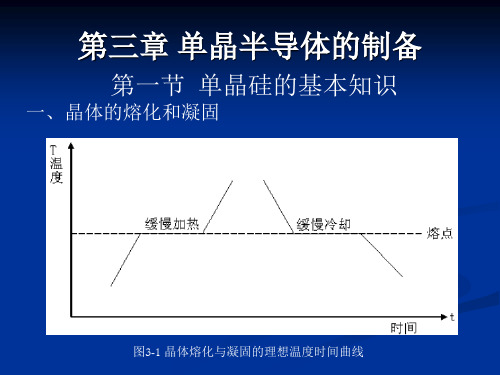
六、晶体的长大
图3-5 固相液相界面模型
第二节直拉法制备单晶硅设备及材料准备
目前常用的制备单晶硅的方法主要有直拉法和悬 浮区熔法两种。直拉法是熔体生长单晶的最常用的一 种方法,其示意图如图3-6所示。
图3-6 直拉法制备单晶硅示意图
一、直拉法制备单晶硅设备
1.直拉单晶炉结构 主要由炉体、电气部分、热系统、水冷系统、 真空系统和氢气装置五大部分组成。
3.硅单晶析出及杂质条纹 直拉硅单晶中由于分凝现象,使得生长界面附 近杂质过饱和有时会出现析出,析出是在硅单晶中 形成散粒(或颗粒)掺杂剂单质的现象。
4.单晶硅中的氧和碳 直拉硅单晶中的氧和碳是一类很重要的杂质, 氧和碳在直拉单晶中,可能形成微沉淀,可能在微 沉淀基础上形成微缺陷,严重影响单晶质量,影响 大规模集成电路性能和制造。 直拉硅单晶一般单晶头部氧浓度高,尾部氧浓 度低,单晶的面中心氧浓度高,边缘氧浓度低。硅 单晶的这种氧浓度分布既受坩埚污染影响,也受拉 晶时氧蒸发和氧分凝效应影响。
四、晶核的形成
晶核的形成有两种方式: (1)自发晶核 由于液体内部过冷,在液体内部自发生成的晶核, 叫做自发晶核。 (2)非自发晶核 晶核不在液体内部自发产生,而是借助于外来固 态物质的帮助,比如在籽晶、坩埚壁、液体中的非溶 性杂质等表面上产生的晶核,叫做非自发晶核。
半导体材料芯片研发PPT
TWO 数据分析
01
Would a man running in the rain, also don't want to put into the arms of the false.
03
Would a man running in the rain, also don't want to put into the arms of the false.
ONE 芯片介绍
输入标题
Life is not waiting for the storm in the past, but learning to dance in the wind and rain. Would a man running in the rain, also don't want to put into the arms of the false.
半导体产业
DEVELOPMENT OF CHIP SEMICONDUCTOR 规划制定全面新政策.推动中国半导体发展
目录
CONs not waiting for the storm in the past, but learning to dance in the wind and rain.
PART TWO
数据分析
Life is not waiting for the storm in the past, but learning to dance in the wind and rain.
DEVELOPMENT OF CHIP SEMICONDUCTOR
DEVELOPMENT OF CHIP SEMICONDUCTOR
dance in.
输入 标题
半导体制造工艺流程通用课件

目录
• 半导体制造概述 • 半导体制造的前处理 • 半导体制造的核心工艺 • 半导体制造的后处理 • 半导体制造的挑战与解决方案 • 半导体制造的发展趋势与未来展望
01
半导体制造概述
半导体制造的定义
半导体制造
指通过一系列精密的物理和化学 工艺,将单晶硅或其他半导体材 料转化为集成电路的过程。
采用高k金属栅极材料, 可以提高芯片的性能和降 低功耗。
新型绝缘材料
采用新型绝缘材料,可以 提高芯片的集成度和可靠 性。
新型封装材料
采用新型封装材料,可以 提高芯片的散热性能和可 靠性。
系统集成与封装技术的发展
系统集成技术
通过系统集成技术,将多个芯片集成在一个封装 内,实现更高的性能和更小的体积。
封装类型
常见的封装类型包括塑料封装、陶瓷封装和金属封装等,它们具有不同的特点和适用范围 。
封装工艺
封装工艺涉及到多个环节,包括芯片贴装、引脚焊接、密封和标记等,每个环节都对保证 芯片的性能和可靠性至关重要。
测试与验证
测试与验证
在半导体制造的后处理过程中,测试与验证是确保芯片性能和质量 的重要环节。
化学气相沉积
总结词
化学气相沉积是通过化学反应在半导体表面形成薄膜的过程。
详细描述
化学气相沉积是在高温下,将气态物质在半导体表面进行化学反应,形成固态薄膜的过程。沉积的薄膜可以作为 绝缘层、导电层或保护层,对半导体器件的性能和稳定性具有重要影响。
04
半导体制造的后处理
金属化
金属化
在半导体制造的后处理过程中,金属化是关键的一步,它 涉及到在芯片表面沉积金属,以实现电路的导电连接。
半导体制造的工艺流程简介
半导体芯片制造技术晶圆制备课件

4.氧含量
控制硅锭中的氧含量水平的均匀性是非常重要 的,而且随着更大的直径尺寸,难度也越来越大。 少量的氧能起到俘获中心的作用,它能束缚硅中的 沾染物。然而,硅锭中过量的氧会影响硅的机械和 电学特性。例如,氧会导致P-N结漏电流的增加,也 会增大MOS器件的漏电流。
硅中的氧含量是通过横断面来检测的,即对硅 晶体结构进行成分的分析。一片有代表性的硅被放 在环氧材料的罐里,然后研磨并抛平使其露出固体 颗粒结构。用化学腐蚀剂使要识别的特定元素发亮 或发暗。样品准备好后,使用透射电镜(TEM)描述 晶体的结构,目前硅片中的氧含量被控制在24到 33ppm。
一旦晶体在切割块上定好晶向,就沿着轴滚磨出 一个参考面,如图4-4所示。
图4-4定位面研磨
图4-5 硅片的类型标志
四、切片
单晶硅在切片时,硅片的厚度,晶向,翘曲度和 平行度是关键参数,需要严格控制。晶片切片的要求 是:厚度符合要求;平整度和弯曲度要小,无缺损, 无裂缝,刀痕浅。
单晶硅切成硅片,通常采用内圆切片机或线切片 机。
图4-18 硅片变形
2.平整度
平整度是硅片最主要的参数之一,主要是因为 光刻工艺对局部位置的平整度是非常敏感的。硅片 平整度是指在通过硅片的直线上的厚度变化。它是 通过硅片的上表面和一个规定参考面的距离得到的。 对一个硅片来说,如果它被完全平坦地放置,参考 面在理论上就是绝对平坦的背面,比如利用真空压 力把它拉到一个清洁平坦的面上,如图4-19所示, 平整度可以规定为硅片上一个特定点周围的局部平 整度,也可以规定为整体平整度,它是在硅片表面 的固定质量面积(FQA)上整个硅片的平整度。固定 质量面积不包括硅片表面周边的无用区域。测量大 面积的平整度要比小面积难控制。
然而,晶圆具有的一个特性却限制了生产商随 意增加晶圆的尺寸,那就是在芯片生产过程中,离 晶圆中心越远就越容易出现坏点,因此从晶圆中心 向外扩展,坏点数呈上升趋势。另外更大直径晶圆 对于单晶棒生长以及芯片制造保持良好的工艺控制 都提出了更高的要求,这样我们就无法随心所欲地 增大晶圆尺寸。
半导体制造工艺技术PPT(共68页)

Si2H6(气态) (反应半
3) Si2H6(气态) 品形成)
2Si (固态) + 3H2(气态) (最终产
以上实例是硅气相外延的一个反应过程
• 速度限制阶段
在实际大批量生产中,CVD反应的时间长 短很重要。温度升高会促使表面反应速度增加 。基于CVD反应的有序性,最慢的反应阶段会 成为整个工艺的瓶颈。换言之,反应速度最慢 的阶段将决定整个淀积过程的速度。
膜对台阶的覆盖
我们期望膜在硅片表面上厚度一致,但由 于硅片表面台阶的存在,如果淀积的膜在台阶 上过渡的变薄,就容易导致高的膜应力、电短 路或在器件中产生不希望的诱生电荷。应力还 可能导致衬底发生凸起或凹陷的变形。
均匀厚度
共形台阶覆盖
非共形台阶覆盖
高的深宽比间隙
可以用深宽比来描述一个小间隙(如槽或孔), 深宽比定义为间隙的深度和宽度的比值(见下图)
Figure 11.7
膜淀积技术
化学工艺
化学气相淀积 (CVD)
常压化学气相淀积 (APCVD)
或亚常压化学气相淀积 (SACVD)
低压化学气相淀积 (LPCVD)
等离子体辅助 CVD ▪ 等离子体增强 CVD
(PECVD) ▪ 高密度等离子体化
学气相淀积 (HDPCVD)
电镀
电化学淀积 (ECD),
个反应。反应1)显示硅烷首先分解成SiH2先驱 物。 SiH2先驱物再和硅烷反应形成Si2H6。在中 间CVD反应中, SiH2随着Si2H6被吸附在硅片表 面。然后Si2H6分解形成最终需要的固态硅膜。
1) SiH4(气态)
SiH2(气态) + H2(气态) (高温分解)
2) SiH4(气态) + SiH2(气态) 成品形成)
最新半导体制造技术第十七章ppt课件
离子注入的优点
1. 精确控制掺杂浓度 2. 很好的杂质均匀性 3. 对杂质深度很好控制 4. 产生单一离子束 5. 低温工艺 6. 注入的离子能穿过薄膜 7. 无固溶度极限
缺点
• 1.辐射损伤。高温退火修复。 • 2.设备复杂(比扩散)
注入剂量
Q It enA
Test/Sort
Wafer fabrication (front-end)
Thin Films
Polish
Diffusion
Photo
Etch
Anneal after implant
Photoresist mask Implant
Hard mask (oxide or nitride)
Used with permission from Lance Kinney, AMD
核阻止和电 子阻止相等 的能量
❖ 核阻止本领在低能量下起主要作用(注入分布的尾端) ❖ 电子阻止本领在高能量下起主要作用
横向效应
杂质与硅原子碰撞所产生的散射会造成杂质往横 向注入。横向效应是指注入离子在垂直入射方向 的平面内的分布情况,会影响MOS管的有效沟道长 度。横向效应与注入离子的种类及入射离子的能 量有关。
杂质离子的射程和投影射程
Incident ion beam
Silicon substrate Rp
Stopping point for a single ion
DRp dopant distribution
Figure 17.7
离子注入机的种类
注入系统分类 中、低电流
大电流 高能 氧注入机
描述和应用
• 选择源必需满足固溶度、扩散系数要求。 • 选择好掩蔽膜。