SN74AVC16T245(16位双向传输电平转换器)
DSP常见问题解答
DSP常见问题解答如何选择外部时钟?DSP的内部指令周期较高,外部晶振的主频不够,因此DSP大多数片内均有PLL。
但每个系列不尽相同。
1)TMS320C2000系列:TMS320C20x:PLL可以÷2,×1,×2和×4,因此外部时钟可以为5MHz-40MHz。
TMS320F240:PLL可以÷2,×1,×1.5,×2,×2.5,×3,×4,×4.5,×5和×9,因此外部时钟可以为2.22MHz-40MHz。
TMS320F241/C242/F243:PLL可以×4,因此外部时钟为5MHz。
TMS320LF24xx:PLL可以由RC调节,因此外部时钟为4MHz-20MHz。
TMS320LF24xxA:PLL可以由RC调节,因此外部时钟为4MHz-20MHz。
2)TMS320C3x系列:TMS320C3x:没有PLL,因此外部主频为工作频率的2倍。
TMS320VC33:PLL可以÷2,×1,×5,因此外部主频可以为12MHz -100MHz。
3)TMS320C5000系列:TMS320VC54xx:PLL可以÷4,÷2,×1-32,因此外部主频可以为0.625MHz-50MHz。
TMS320VC55xx:PLL可以÷4,÷2,×1-32,因此外部主频可以为6.25MHz-300MHz。
4)TMS320C6000系列:TMS320C62xx:PLL可以×1,×4,×6,×7,×8,×9,×10和×11,因此外部主频可以为11.8MHz-300MHz。
TMS320C67xx:PLL可以×1和×4,因此外部主频可以为12.5MHz-230MHz。
74HC245电路

细的参数规格及各厂商型号替换,请以厂商数据手册为准。
生产工艺
TI 公司
ON 公司
工作电压(V)
输入电平兼容
输出电平兼容
74F
F
4.5~5.5
TTL
TTL
Bipolar 5V-Logic
LS
LS
4.75~5.25
TTL
TTL
ALS
4.5~5.5
TTL
TTL
CD4000 系列
MC1400 系列
3.0~18
DFT2,XV5T2
DTT1,DFT2
US
z 工业级温度范围: -40~85℃
07
Buffer OD
DFT2,XV5T2
DTT1,DFT2
US
08
2-Input AND
DFT2,XV5T2
US
14
Inverter-Schmitt
DFT2,XV5T2
DTT1,DFT2
US
数
优点
16
Buffer
DFT2,XV5T2
150
产品参数仅供参考,以厂家数据手册为准。批量价格,欢迎垂询。更多详情:
免费业务电话:800-880-8051 总机:027-8752 6752 传真:027-8752 6551
CMOS
CMOS
HC
HC
2.0~6.0
CMOS
CMOS
AHC
VHC
2.0~5.5
CMOS
CMOS
AHC1G
MC74VHC1G
2.0~6.0
CMOS
CMOS
CMOS 5V-Logic
HCT
HCT
4.5~5.5
74lvc245中文说明
74LV245是低压硅栅CMOS器件,与74HC245和74HCT245针脚和功能兼容。
74LV245是八位元收发器,在发送和接收方向上都具有非反相3态总线兼容输出。
发送/接收(DIR)输入控制方向,而输出使能(OE)输入则可实现轻松级联。
针脚OE控制输出,因此总线可以得到有效隔离。
特性和优势
•宽工作电压范围:1.0 V至5.5 V
•最适合低压应用:1.0 V至3.6 V
•接受介于VCC = 2.7 V和VCC = 3.6 V之间的TTL输入电平
•VCC = 3.3 V且T amb = 25 °C时的典型输出地弹:< 0.8 V
•VCC = 3.3 V且T amb = 25 °C时的典型高电平输出电压(VOH)欠冲:> 2 V •ESD保护:
o HBM JESD22-A114E超过2000 V
o MM JESD22-A115-A超过200 V
•多种封装选择
•额定温度范围为-40 °C至+85 °C和-40 °C至+125 °C
外形图
显示功能框图
真值表
INPUTS INPUTS/OUTPUT OE DIR An Bn
H=高电压L=低电压X=无输入、Z=高阻态。
74AVC8T245 8位数据双向电平转换IC
Supply voltage
Input
VCC(A), VCC(B) 0.8 V to 3.6 V
OE[2] L
0.8 V to 3.6 V
L
0.8 V to 3.6 V
H
GND[3]
X
DIR[2] L H X X
Input/output[3] An[2] An = Bn input Z Z
[1] H = HIGH voltage level; L = LOW voltage level; X = don’t care; Z = high-impedance OFF-state. [2] The An, DIR and OE input circuit is referenced to VCC(A); The Bn input circuit is referenced to VCC(B). [3] If at least one of VCC(A) or VCC(B) is at GND level, the device goes into suspend mode.
NXP Semiconductors
74AVC8T245
8-bit dual supply translating transceiver; 3-state
I Suspend mode I Latch-up performance exceeds 100 mA per JESD 78 Class II I Inputs accept voltages up to 3.6 V I IOFF circuitry provides partial Power-down mode operation I Multiple package options I Specified from −40 °C to +85 °C and −40 °C to +125 °C
德尔福汽车仪表拆解报告+结构设计update

德尔福汽车仪表拆解报告1、汽车仪表后盖图后盖上可以看到电源及总线接口以及预留RGB串行化显示的接口。
2、卸掉后盖螺丝之后,可以看到PCB的正反面全貌,整体比较整洁,采用一块PCB 板,所有的元器件采用类似苹果产品的方法,去掉了丝印。
正面反面3、整机的ESD及结构设计无论是PCB还是外壳,我们可以看到,ESD设计非常好,主机板的放电回路无论是正面还是反面都通过8个螺丝孔与外壳充分的接触。
ESD放电螺丝孔金属垫片设计LED指示灯并非传统的通过排线引出PCB的设计,而是采用导光槽,LED光通过导光槽之后,均匀的投射到碳膜指示区域。
LED导光槽设计4、整机硬件架构分析1)CPU:Freescale i.mx51车规级芯片(MCIMX514AJM6C)主频:600MH z2) DDR: micron DDR2 256M3) eMMC: ST 16G4) Norflash: Spanion 256M5) 电源方案:B+电源方案:B+电源进入之后的方案较为简单,通过两个防反接的二极管之后,分别使用了2颗470UF的铝电解和一颗cooper的电感,具体参数如下。
DRA 系列磁性屏蔽磁鼓芯电感器,具有高功率密度和高效性,适用于汽车应用。
DRA 系列电感器设计带有铁氧体磁芯,可牢固安装,适用于高冲击和振动环境。
DRA 系列的应用包括:汽车电子(用于罩盖下,内部/外部);车载信息服务;直流到直流转换器;降压、升压、正向和谐振转换器;噪音过滤和滤波器扼流圈,165°C 最高工作温度。
第一级电源方案(12V降压到5V):一部分提供给MCU工作,另外一部分提供给其他的DC/DC电源作为输入电源TPS54362 车规级电源芯片。
3A,可耐压为60V,规格书开关频率为:200K~2.2MHz。
德尔福设置开关频率为500KHz,输入端都采用了470UF的nichicon的铝电解电容。
CPU及周边供电:使用了两颗车规级芯片TPS65023:3路DC/DC 系统供电3.3V,memory供电1.8V,CPU供电 1.2V3路DC/DC CPU供电2.775V,CPU供电1.05V,一路NC开关频率固定为2.25Mhz,在power save状态下,可以依据负载电流的不同而在750K到2.25MHz之间变化。
sn74lvc16t245-(适合国防与航空航天)
1 2 3 4 5 6 7 8 9 10 11 12 13 14 15 16 17 18 19 20 21 22 23 2448 47 46 45 44 43 42 41 40 39 38 37 36 35 34 33 32 31 30 29 28 27 26 251DIR 1B1 1B2 GND 1B3 1B4 V CCB 1B5 1B6 GND 1B7 1B8 2B1 2B2 GND 2B3 2B4 V CCB 2B5 2B6 GND 2B7 2B8 2DIR1OE1A11A2GND1A31A4V CCA1A51A6GND1A71A82A12A2GND2A32A4V CCA2A52A6GND2A72A82OESN74LVC16T245-EP ZHCSAQ3A–JANUARY2013–REVISED FEBRUARY201316位双电源总线收发器此收发器具有可配置电压转换和三态输出查询样品:SN74LVC16T245-EP特性DGG封装•控制输入V IH和V IL电平以V CCA电压为基准(顶视图)•V CC隔离特性-如果任何一个V CC输入接地(GND),那么两个端口都处于高阻抗状态•过压耐受输入和输出可实现混合电压模式数据通信•完全可配置双电源轨设计可使每个端口在整个1.65V-5.5V电源电压范围内运行•I关闭支持部分断电模式工作•锁断性能超过100mA(符合JESD78,II类规范的要求)•静电放电(ESD)保护性能超过JESD22规范要求–2000V人体模型(A114-A)–200V机器模型(A115-A)–1000V充电器件模型(C101)支持国防、航空航天、和医疗应用•受控基线•一个组装和测试场所•一个制造场所•军用(-55°C至125°C)温度范围内可用(1)•延长的产品生命周期•延长的产品变更通知•产品可追溯性(1)可定制工作温度范围说明这个16位非反相总线收发器使用两个独立的可配置电源轨。
75HC245规格书
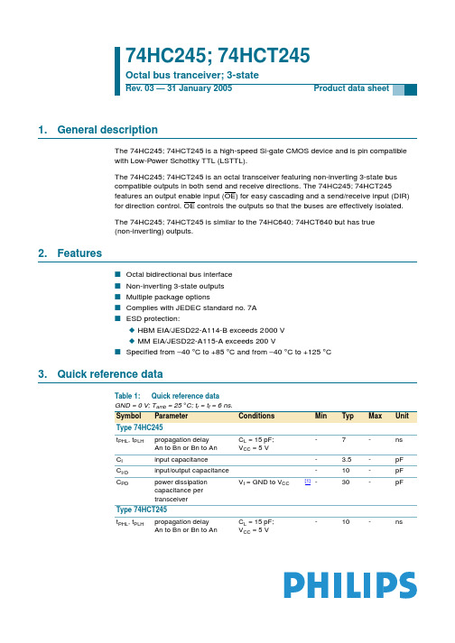
1.General descriptionThe 74HC245; 74HCT245 is a high-speed Si-gate CMOS device and is pin compatible with Low-Power Schottky TTL (LSTTL).The 74HC245; 74HCT245 is an octal transceiver featuring non-inverting 3-state bus compatible outputs in both send and receive directions. The 74HC245; 74HCT245features an output enable input (OE) for easy cascading and a send/receive input (DIR)for direction control.OE controls the outputs so that the buses are effectively isolated.The 74HC245; 74HCT245 is similar to the 74HC640; 74HCT640 but has true (non-inverting) outputs.2.Featuress Octal bidirectional bus interface s Non-inverting 3-state outputs s Multiple package optionss Complies with JEDEC standard no. 7A sESD protection:x HBM EIA/JESD22-A114-B exceeds 2000V x MM EIA/JESD22-A115-A exceeds 200Vs Specified from −40°C to +85°C and from −40°C to +125°C3.Quick reference data74HC245; 74HCT245Octal bus tranceiver; 3-stateRev. 03 — 31 January 2005Product data sheetTable 1:Quick reference data GND =0V; T amb =25°C; t r =t f =6 ns.Symbol ParameterConditions Min Typ Max Unit Type 74HC245t PHL , t PLH propagation delay An to Bn or Bn to An C L =15pF;V CC =5V-7-ns C I input capacitance - 3.5-pF C I/O input/output capacitance -10-pF C PDpower dissipation capacitance per transceiverV I =GND to V CC[1]-30-pFType 74HCT245t PHL , t PLHpropagation delay An to Bn or Bn to AnC L =15pF;V CC =5V-10-ns[1]C PD is used to determine the dynamic power dissipation (P D in µW):P D =C PD ×V CC 2×f i ×N +∑ (C L ×V CC 2×f o ) where:f i =input frequency in MHz;f o =output frequency in MHz;C L =output load capacitance in pF;V CC =supply voltage in V;N =number of inputs switching;∑(C L ×V CC 2×f o )=sum of outputs.4.Ordering informationC I input capacitance - 3.5-pF C I/O input/output capacitance -10-pF C PDpower dissipation capacitance per transceiverV I =GND to V CC −1.5V[1]-30-pFTable 1:Quick reference data …continued GND =0V; T amb =25°C; t r =t f =6 ns.Symbol Parameter Conditions Min Typ Max Unit Table 2:Ordering informationType numberPackageTemperature range NameDescriptionVersion 74HC245N −40°C to +125°C DIP20plastic dual in-line package; 20leads (300 mil)SOT146-174HC245D −40°C to +125°C SO20plastic small outline package; 20leads;body width 7.5mmSOT163-174HC245PW −40°C to +125°C TSSOP20plastic thin shrink small outline package; 20leads;body width 4.4mmSOT360-174HC245DB −40°C to +125°C SSOP20plastic shrink small outline package; 20leads;body width 5.3mmSOT339-174HC245BQ−40°C to +125°CDHVQFN20plastic dual-in-line compatible thermal enhanced very thin quad flat package no leads;20terminals;body 2.5×4.5×0.85mm SOT764-174HCT245N −40°C to +125°C DIP20plastic dual in-line package; 20leads (300 mil)SOT146-174HCT245D −40°C to +125°C SO20plastic small outline package; 20leads;body width 7.5mmSOT163-174HCT245PW −40°C to +125°C TSSOP20plastic thin shrink small outline package; 20leads;body width 4.4mmSOT360-174HCT245DB −40°C to +125°C SSOP20plastic shrink small outline package; 20leads;body width 5.3mmSOT339-174HCT245BQ−40°C to +125°CDHVQFN20plastic dual-in-line compatible thermal enhanced very thin quad flat package no leads;20terminals;body 2.5×4.5×0.85mmSOT764-15.Functional diagramFig 1.Logic symbol Fig 2.IEC logic symbol21DIR1819B0B1B2B3B4B5B6B73174165156147138129A0A1A2A3A4A5A6A711OEmna1741731192116415514613712811918G33EN13EN22mna1756.Pinning information6.1Pinning6.2Pin description(1)The die substrate is attached to thispad using conductive die attachmaterial. It can not be used as supply pin or inputFig 3.Pin configuration DIP20, SO20,SSOP20 and TSSOP20Fig 4.Pin configuration DHVQFN20245DIR V CC A0OE A1B0A2B1A3B2A4B3A5B4A6B5A7B6GND B7001aac4311234567891012111413161518172019001aac432245GND (1)Transparent top viewB6A6A7B5A5B4A4B3A3B2A2B1A1B0A0OE G N D B 7D I RV C C9128137146155164173182191011120terminal 1index areaTable 3:Pin descriptionSymbol Pin Description DIR 1direction control A02data input/output A13data input/output A24data input/output A35data input/output A46data input/output A57data input/output A68data input/output A79data input/output GND 10ground (0V)B711data input/output B612data input/output B513data input/output B414data input/output B315data input/output B216data input/output7.Functional description7.1Function table[1]H =HIGH voltage level;L =LOW voltage level;X =don’t care;Z =high-impedance OFF-state.8.Limiting values[1]For DIP20 packages: above 70°C, P tot derates linearly with 12mW/K.For SO20 packages: above 70°C, P tot derates linearly with 8mW/K.For SSOP20 and TSSOP20 packages: above 60°C, P tot derates linearly with 5.5mW/K.For DHVQFN20 packages: above 60°C, P tot derates linearly with 4.5mW/K.B117data input/output B018data input/outputOE 19output enable input (active LOW)V CC20supply voltageTable 3:Pin description …continuedSymbol Pin Description Table 4:Function table [1]Input Input/outputOE DIR An Bn L L A = B input L H input B = A HXZZTable 5:Limiting valuesIn accordance with the Absolute Maximum Rating System (IEC 60134). Voltages are referenced to GND (ground = 0 V).Symbol Parameter ConditionsMin Max Unit V CC supply voltage −0.5+7V I IK input diode current V I <−0.5V or V I >V CC +0.5 V -±20mA I OK output diode current V O <−0.5V or V O >V CC +0.5V-±20mA I O output source or sink currentV O =−0.5V to V CC +0.5V-±35mA I CC , I GND V CC or GND current -±70mA T stg storage temperature −65+150°C P tottotal power dissipation [1]DIP20 package -750mW SO20, SSOP20,TSSOP20 andDHVQFN20 packages-500mW9.Recommended operating conditions10.Static characteristicsTable 6:Recommended operating conditions Symbol Parameter ConditionsMin Typ Max Unit Type 74HC245V CC supply voltage 2.0 5.0 6.0V V I input voltage 0-V CC V V O output voltage 0-V CC V t r , t finput rise and fall timesV CC = 2.0 V --1000ns V CC = 4.5 V - 6.0500ns V CC = 6.0 V--400ns T amb ambient temperature −40-+125°CType 74HCT245V CC supply voltage 4.5 5.0 5.5V V I input voltage 0-V CC V V O output voltage 0-V CC V t r , t f input rise and fall timesV CC = 4.5 V- 6.0500ns T ambambient temperature−40-+125°CTable 7:Static characteristics type 74HC245At recommended operating conditions; voltages are referenced to GND (ground =0V).Symbol ParameterConditions Min Typ Max Unit T amb =25°CV IHHIGH-level input voltageV CC =2.0V 1.5 1.2-V V CC =4.5V 3.15 2.4-V V CC =6.0V4.2 3.2-V V ILLOW-level input voltageV CC =2.0V -0.80.5V V CC =4.5V - 2.1 1.35V V CC =6.0V- 2.81.8VV OHHIGH-level output voltageV I =V IH or V ILI O =−20µA; V CC =2.0V 1.9 2.0-V I O =−20µA; V CC =4.5V 4.4 4.5-V I O =−20µA; V CC =6.0V 5.9 6.0-V I O =−6.0mA; V CC =4.5V 3.98 4.32-V I O =−7.8mA; V CC =6.0V5.485.81-VV OLLOW-level output voltageV I =V IH or V ILI O =20µA; V CC =2.0V -00.1V I O =20µA; V CC =4.5V -00.1V I O =20µA; V CC =6.0V -00.1V I O =6.0mA; V CC =4.5V -0.150.26V I O =7.8mA; V CC =6.0V-0.160.26V I LI input leakage current V I =V CC or GND; V CC =6.0V --±0.1µA I OZ OFF-state output current V I =V IH or V IL ; V O =V CC or GND;V CC =6.0V--±0.5µA I CC quiescent supply current V I =V CC or GND; I O =0A;V CC =6.0V--8.0µA C I input capacitance - 3.5-pF C I/O input/output capacitance -10-pF T amb =−40°C to +85°CV IHHIGH-level input voltageV CC =2.0V 1.5--V V CC =4.5V 3.15--V V CC =6.0V4.2--V V ILLOW-level input voltageV CC =2.0V --0.5V V CC =4.5V -- 1.35V V CC =6.0V-- 1.8V V OHHIGH-level output voltageV I =V IH or V ILI O =−20µA; V CC =2.0V 1.9--V I O =−20µA; V CC =4.5V 4.4--V I O =−20µA; V CC =6.0V 5.9--V I O =−6.0mA; V CC =4.5V 3.84--V I O =−7.8mA; V CC =6.0V5.34--V V OLLOW-level output voltageV I =V IH or V ILI O =20µA; V CC =2.0V --0.1V I O =20µA; V CC =4.5V --0.1V I O =20µA; V CC =6.0V --0.1V I O =6.0mA; V CC =4.5V --0.33V I O =7.8mA; V CC =6.0V--0.33V I LI input leakage current V I =V CC or GND; V CC =6.0V --±1.0µA I OZ OFF-state output current V I =V IH or V IL ; V O =V CC or GND;V CC =6.0V--±5.0µA I CCquiescent supply currentV I =V CC or GND; I O =0A;V CC =6.0V --80µAT amb =−40°C to +125°C V IHHIGH-level input voltageV CC =2.0V 1.5--V V CC =4.5V 3.15--V V CC =6.0V4.2--VTable 7:Static characteristics type 74HC245 …continuedAt recommended operating conditions; voltages are referenced to GND (ground =0V).Symbol ParameterConditions Min Typ Max UnitV IL LOW-level input voltage V CC=2.0V--0.5VV CC=4.5V-- 1.35VV CC=6.0V-- 1.8V V OH HIGH-level output voltage V I=V IH or V IL-I O=−20µA; V CC=2.0V 1.9--VI O=−20µA; V CC=4.5V 4.4--VI O=−20µA; V CC=6.0V 5.9--VI O=−6.0mA; V CC=4.5V 3.7--VI O=−7.8mA; V CC=6.0V 5.2--V V OL LOW-level output voltage V I=V IH or V IL-I O=20µA; V CC=2.0V--0.1VI O=20µA; V CC=4.5V--0.1VI O=20µA; V CC=6.0V--0.1VI O=6.0mA; V CC=4.5V--0.4VI O=7.8mA; V CC=6.0V--0.4V I LI input leakage current V I=V CC or GND; V CC=6.0V--±1.0µA I OZ OFF-state output current V I=V IH or V IL; V O=V CC or GND;V CC=6.0V--±10.0µAI CC quiescent supply current V I=V CC or GND; I O=0A;V CC=6.0V --160µATable 7:Static characteristics type 74HC245 …continuedAt recommended operating conditions; voltages are referenced to GND (ground=0V).Symbol Parameter Conditions Min Typ Max Unit Table 8:Static characteristics type 74HCT245At recommended operating conditions; voltages are referenced to GND (ground=0V).Symbol Parameter Conditions Min Typ Max Unit T amb=25°CV IH HIGH-level input voltage V CC=4.5V to 5.5V 2.0 1.6-VV IL LOW-level input voltage V CC=4.5V to 5.5V- 1.20.8VV OH HIGH-level output voltage V I=V IH or V IL; V CC=4.5VI O=−20µA 4.4 4.5-VI O=−6mA 3.98 4.32-VV OL LOW-level output voltage V I=V IH or V IL; V CC=4.5VI O=20µA-00.1VI O=6.0mA-0.150.26VI LI input leakage current V I=V CC or GND; V CC=5.5V--±0.1µA I OZ OFF-state output current V I=V IH or V IL; V CC=5.5V;V O=V CC or GND per input pin;other inputs at V CC or GND;I O=0A--±0.5µAI CC quiescent supply current V I=V CC or GND; I O=0A;V CC=5.5V--8.0µA∆I CC additional quiescent supplycurrent per input pin V I=V CC−2.1V; other inputs at V I=V CC or GND;V CC=4.5V to5.5V; I O=0AAn or Bn inputs-40144µAOE input-150540µADIR input-90324µA C I input capacitance- 3.5-pF C I/O input/output capacitance-10-pF T amb=−40°C to +85°CV IH HIGH-level input voltage V CC=4.5V to 5.5V 2.0--V V IL LOW-level input voltage V CC=4.5V to 5.5V--0.8V V OH HIGH-level output voltage V I=V IH or V IL; V CC=4.5VI O=−20µA 4.4--VI O=−6mA 3.84--V V OL LOW-level output voltage V I=V IH or V IL; V CC=4.5VI O=20µA--0.1VI O=6.0mA--0.33V I LI input leakage current V I=V CC or GND; V CC=5.5V--±1.0µA I OZ OFF-state output current V I=V IH or V IL; V CC=5.5V;V O=V CC or GND per input pin;other inputs at V CC or GND;I O=0A--±5.0µAI CC quiescent supply current V I=V CC or GND; I O=0A;V CC=5.5V--80µA∆I CC additional quiescent supplycurrent per input pin V I=V CC−2.1V; other inputs at V I=V CC or GND;V CC=4.5V to5.5V; I O=0AAn or Bn inputs--180µAOE input--675µADIR input--405µA T amb=−40°C to +125°CV IH HIGH-level input voltage V CC=4.5V to 5.5V 2.0--V V IL LOW-level input voltage V CC=4.5V to 5.5V--0.8V V OH HIGH-level output voltage V I=V IH or V IL; V CC=4.5VI O=−20µA 4.4--VI O=−6mA 3.7--V V OL LOW-level output voltage V I=V IH or V IL; V CC=4.5VI O=20µA--0.1VI O=6.0mA--0.4V I LI input leakage current V I=V CC or GND; V CC=5.5V--±1.0µAI OZ OFF-state output current V I=V IH or V IL; V CC=5.5V;V O=V CC or GND per input pin;other inputs at V CC or GND;I O=0A --±10µATable 8:Static characteristics type 74HCT245 …continuedAt recommended operating conditions; voltages are referenced to GND (ground=0V).Symbol Parameter Conditions Min Typ Max Unit11.Dynamic characteristicsI CC quiescent supply current V I =V CC or GND; I O =0A;V CC =5.5V--160µA∆I CCadditional quiescent supply current per input pin V I =V CC −2.1V; other inputs at V I =V CC or GND;V CC =4.5V to 5.5V; I O =0AAn or Bn inputs --196µA OE input --735µA DIR input--441µATable 8:Static characteristics type 74HCT245 …continuedAt recommended operating conditions; voltages are referenced to GND (ground =0V).Symbol ParameterConditionsMin Typ Max Unit Table 9:Dynamic characteristics type 74HC245GND =0V; test circuit see Figure 7.Symbol ParameterConditionsMinTypMaxUnitT amb = 25°Ct PHL , t PLHpropagation delay An to Bn or Bn to An see Figure 5V CC = 2.0 V-2590ns V CC = 4.5 V-918ns V CC = 5.0 V; C L =15pF -7-ns V CC = 6.0 V-715ns t PZH , t PZL3-state output enable time OE to An or OE to Bnsee Figure 6V CC = 2.0 V -30150ns V CC = 4.5 V -1130ns V CC = 6.0 V-926ns t PHZ , t PLZ3-state output disable time OE to An or OE to Bnsee Figure 6V CC = 2.0 V -41150ns V CC = 4.5 V -1530ns V CC = 6.0 V-1226ns t THL , t TLHoutput transition timesee Figure 5V CC = 2.0 V -1460ns V CC = 4.5 V -512ns V CC = 6.0 V-410ns C PDpower dissipation capacitance per transceiverV I =GND to V CC[1]-30-pFT amb =−40°C to +85°C t PHL , t PLHpropagation delay An to Bn or Bn to An see Figure 5V CC = 2.0 V--115ns V CC = 4.5 V --23ns V CC = 6.0 V--20ns[1]C PD is used to determine the dynamic power dissipation (P D in µW):P D =C PD ×V CC 2×f i ×N +∑ (C L ×V CC 2×f o ) where:f i =input frequency in MHz;f o =output frequency in MHz;C L =output load capacitance in pF;V CC =supply voltage in V;N =number of inputs switching;∑(C L ×V CC 2×f o )=sum of outputs.t PZH , t PZL3-state output enable time OE to An or OE to Bnsee Figure 6V CC = 2.0 V --190ns V CC = 4.5 V --38ns V CC = 6.0 V--33ns t PHZ , t PLZ3-state output disable time OE to An or OE to Bnsee Figure 6V CC = 2.0 V --190ns V CC = 4.5 V --38ns V CC = 6.0 V--33ns t THL , t TLHoutput transition timesee Figure 5V CC = 2.0 V --75ns V CC = 4.5 V --15ns V CC = 6.0 V--13nsT amb =−40°C to +125°C t PHL , t PLHpropagation delay An to Bn or Bn to An see Figure 5V CC = 2.0 V--135ns V CC = 4.5 V --27ns V CC = 6.0 V--23ns t PZH , t PZL3-state output enable time OE to An or OE to Bnsee Figure 6V CC = 2.0 V --225ns V CC = 4.5 V --45ns V CC = 6.0 V--38ns t PHZ , t PLZ3-state output disable time OE to An or OE to Bnsee Figure 6V CC = 2.0 V --225ns V CC = 4.5 V --45ns V CC = 6.0 V--38ns t THL , t TLHoutput transition timesee Figure 5V CC = 2.0 V --90ns V CC = 4.5 V --18ns V CC = 6.0 V--15nsTable 9:Dynamic characteristics type 74HC245 …continued GND =0V; test circuit see Figure 7.Symbol ParameterConditions Min Typ Max Unit[1]C PD is used to determine the dynamic power dissipation (P D in µW):P D =C PD ×V CC 2×f i ×N +∑ (C L ×V CC 2×f o ) where:f i =input frequency in MHz;f o =output frequency in MHz;C L =output load capacitance in pF;V CC =supply voltage in V;N =number of inputs switching;∑(C L ×V CC 2×f o )=sum of outputs.Table 10:Dynamic characteristics type 74HCT245GND =0V; test circuit see Figure 7.Symbol ParameterConditionsMinTypMaxUnitT amb = 25°Ct PHL , t PLHpropagation delay An to Bn or Bn to An see Figure 5V CC = 4.5 V-1222ns V CC = 5.0 V; C L =15pF-10-ns t PZH , t PZL 3-state output enable time OE to An or OE to BnV CC = 4.5 V; see Figure 6-1630ns t PHZ , t PLZ 3-state output disable time OE to An or OE to Bn V CC = 4.5 V; see Figure 6-1630ns t THL , t TLH output transition timeV CC = 4.5 V; see Figure 5-512ns C PDpower dissipation capacitance per transceiverV I =GND to V CC −1.5V[1]-30-pFT amb =−40°C to +85°C t PHL , t PLH propagation delay An to Bn or Bn to AnV CC = 4.5 V; see Figure 5--28ns t PZH , t PZL 3-state output enable time OE to An or OE to BnV CC = 4.5 V; see Figure 6--38ns t PHZ , t PLZ 3-state output disable time OE to An or OE to Bn V CC = 4.5 V; see Figure 6--38ns t THL , t TLH output transition timeV CC = 4.5 V; see Figure 5--15ns T amb =−40°C to +125°Ct PHL , t PLH propagation delay An to Bn or Bn to AnV CC = 4.5 V; see Figure 5--33ns t PZH , t PZL 3-state output enable time OE to An or OE to BnV CC = 4.5 V; see Figure 6--45ns t PHZ , t PLZ 3-state output disable time OE to An or OE to Bn V CC = 4.5 V; see Figure 6--45ns t THL , t TLHoutput transition timeV CC = 4.5 V; see Figure 5--18ns12.WaveformsMeasurement points are given in Table 11.V OL and V OH are typical voltage output drop that occur with the output load.Fig 5.Input (An, Bn) to output (Bn, An) propagation delays and output transition timesMeasurement points are given in Table 11.V OL and V OH are typical voltage output drop that occur with the output load.Fig 6.3-state output enable and disable times Table 11:Measurement pointsType Input Output V M V M 74HC2450.5V CC 0.5V CC 74HCT2451.3V1.3V001aac433t PLH t PHLV M V M90 %10 %V M V MBn, An outputAn, Bn inputV IGNDV OHV OLt TLHt THL001aac479t PLZt PHZoutputs disabledoutputs enabled90 %10 %outputs enabledOE inputV IV CCV OLV OHGND GNDV Mt PZLt PZHV MV Moutput LOW-to-OFF OFF-to-LOWoutput HIGH-to-OFF OFF-to-HIGHt rt f90 %10 %Test data is given in T able 12.Definitions test circuit:R T = Termination resistance should be equal to output impedance Z o of the pulse generator.C L = Load capacitance including jig and probe capacitance.R L = Load resistor.Fig 7.Load circuitry for switching times Table 12:Test dataType Input Test V I t r , t f t PHL , t PLH t PZH , t PHZ t PZL , t PLZ 74HC245V CC 6ns open GND V CC 74HCT2453V6nsopenGNDV CCmgk563D.U.T V CCV CCV IV OR TR L = 1 k ΩC L 50 pFopenPULSE GENERATOR13.Package outlineFig 8.Package outline SOT146-1 (DIP20)UNIT Amax.12b 1c DEe M H L REFERENCESOUTLINE VERSION EUROPEAN PROJECTIONISSUE DATE IECJEDEC JEITA mm inchesDIMENSIONS (inch dimensions are derived from the original mm dimensions)SOT146-199-12-2703-02-13A min. A max.b Z max.w M E e 11.731.300.530.380.360.2326.9226.54 6.406.22 3.603.050.2542.547.628.257.8010.0 8.324.20.51 3.20.0680.0510.0210.0150.0140.0091.0601.0450.250.240.140.120.010.10.30.320.310.390.330.0780.170.020.13SC-603MS-001M Hc(e )1M EALs e a t i n g p l a n eA 1w Mb 1eDA 2Z2011110bEpin 1 index0510 mmscaleNote1. Plastic or metal protrusions of 0.25 mm (0.01 inch) maximum per side are not included.(1)(1)(1)DIP20: plastic dual in-line package; 20 leads (300 mil)SOT146-1Fig 9.Package outline SOT163-1 (SO20)UNIT A max.A 1A 2A 3b p c D (1)E (1)(1)e H E L L p Q Zy w v θREFERENCESOUTLINEVERSION EUROPEAN PROJECTIONISSUE DATE IEC JEDEC JEITAmm inches 2.650.30.12.452.250.490.360.320.2313.012.67.67.4 1.2710.6510.001.11.00.90.48oo 0.250.1DIMENSIONS (inch dimensions are derived from the original mm dimensions)Note1. Plastic or metal protrusions of 0.15 mm (0.006 inch) maximum per side are not included.1.10.4SOT163-11020w Mb pdetail XZ e111D y0.25 075E04MS-013pin 1 index0.10.0120.0040.0960.0890.0190.0140.0130.0090.510.490.300.290.051.40.0550.4190.3940.0430.0390.0350.0160.010.250.010.0040.0430.0160.010510 mmscaleXθAA 1A 2H EL p QE cLv M A(A )3ASO20: plastic small outline package; 20 leads; body width 7.5 mm SOT163-199-12-2703-02-19Fig 10.Package outline SOT339-1 (SSOP20)UNIT A 1A 2A 3b p c D (1)E (1)e H E L L p Q (1)Z y w v θ REFERENCESOUTLINE VERSION EUROPEAN PROJECTIONISSUE DATE IECJEDEC JEITAmm0.210.051.801.650.380.250.200.097.47.05.45.20.657.97.60.90.70.90.580oo 0.131.250.20.1DIMENSIONS (mm are the original dimensions)Note1. Plastic or metal protrusions of 0.2 mm maximum per side are not included.1.030.63SOT339-1MO-15099-12-2703-02-19Xw MθAA 1A 2b pD H EL p Qdetail XE Z ecLv M A(A )3A1102011y0.25pin 1 index0 2.5 5 mmscaleSSOP20: plastic shrink small outline package; 20 leads; body width 5.3 mm SOT339-1Amax.2Fig 11.Package outline SOT360-1 (TSSOP20)UNIT A 1A 2A 3b p c D (1)E (2)(1)e H E L L p Q Z y w v θ REFERENCESOUTLINE VERSION EUROPEAN PROJECTIONISSUE DATE IECJEDEC JEITAmm0.150.050.950.800.300.190.20.16.66.44.54.30.656.66.20.40.30.50.280oo 0.130.10.21DIMENSIONS (mm are the original dimensions)Notes1. Plastic or metal protrusions of 0.15 mm maximum per side are not included.2. Plastic interlead protrusions of 0.25 mm maximum per side are not included.0.750.50SOT360-1MO-15399-12-2703-02-19w Mb pD Ze0.251102011pin 1 indexθAA 1A 2L p Qdetail XL(A )3H EE cv M AXAy0 2.5 5 mmscaleTSSOP20: plastic thin shrink small outline package; 20 leads; body width 4.4 mm SOT360-1Amax.1.1Fig 12.Package outline SOT764-1 (DHVQFN20)terminal 1index area0.51A 1E h b UNIT y e 0.2c REFERENCESOUTLINE VERSION EUROPEAN PROJECTIONISSUE DATE IEC JEDEC JEITA mm 4.64.4D h 3.152.85y 12.62.41.150.85e 13.50.300.180.050.000.050.1DIMENSIONS (mm are the original dimensions) SOT764-1MO-241- - -- - -0.50.3L 0.1v 0.05w 02.5 5 mmscaleSOT764-1DHVQFN20: plastic dual in-line compatible thermal enhanced very thin quad flat package; no leads;20 terminals; body 2.5 x 4.5 x 0.85 mmA (1)max.AA 1cdetail Xyy 1Ce LE hD he e 1b2919121110120XD EC B Aterminal 1index areaA C CB v M w M E (1)Note1. Plastic or metal protrusions of 0.075 mm maximum per side are not included.D (1)02-10-1703-01-2714.Revision history Table 13:Revision historyDocument ID Releasedate Data sheet status ChangenoticeDoc. number Supersedes74HC_HCT245_320050131Product data sheet-9397 750 1450274HC_HCT245_CNV_2 Modifications:•The format of this data sheet is redesigned to comply with the new presentation andinformation standard of Philips Semiconductors•Section 4 “Ordering information”,Section 6 “Pinning information” and Section 13 “Packageoutline” are modified to include the DHVQFN20 package.74HC_HCT245_CNV_219930930Product specification---9397 750 14502© Koninklijke Philips Electronics N.V . 2005. All rights reserved.Product data sheet Rev. 03 — 31 January 200521 of 2215.Data sheet status[1]Please consult the most recently issued data sheet before initiating or completing a design.[2]The product status of the device(s) described in this data sheet may have changed since this data sheet was published. The latest information is available on the Internet at URL .[3]For data sheets describing multiple type numbers, the highest-level product status determines the data sheet status.16.DefinitionsShort-form specification —The data in a short-form specification is extracted from a full data sheet with the same type number and title. For detailed information see the relevant data sheet or data handbook.Limiting values definition — Limiting values given are in accordance with the Absolute Maximum Rating System (IEC 60134). Stress above one or more of the limiting values may cause permanent damage to the device.These are stress ratings only and operation of the device at these or at any other conditions above those given in the Characteristics sections of the specification is not implied. Exposure to limiting values for extended periods may affect device reliability.Application information — Applications that are described herein for any of these products are for illustrative purposes only. Philips Semiconductors make no representation or warranty that such applications will be suitable for the specified use without further testing or modification.17.DisclaimersLife support —These products are not designed for use in life support appliances, devices, or systems where malfunction of these products can reasonably be expected to result in personal injury. Philips Semiconductors customers using or selling these products for use in such applications do so at their own risk and agree to fully indemnify Philips Semiconductors for any damages resulting from such application.Right to make changes —Philips Semiconductors reserves the right to make changes in the products - including circuits, standard cells, and/or software - described or contained herein in order to improve design and/or performance. When the product is in full production (status ‘Production’),relevant changes will be communicated via a Customer Product/Process Change Notification (CPCN). Philips Semiconductors assumes noresponsibility or liability for the use of any of these products, conveys no license or title under any patent, copyright, or mask work right to theseproducts,and makes no representations or warranties that these products are free from patent,copyright,or mask work right infringement,unless otherwise specified.18.Contact informationFor additional information, please visit: For sales office addresses, send an email to: sales.addresses@Level Data sheet status [1]Product status [2][3]DefinitionI Objective data Development This data sheet contains data from the objective specification for product development. Philips Semiconductors reserves the right to change the specification in any manner without notice.IIPreliminary dataQualificationThis data sheet contains data from the preliminary specification.Supplementary data will be published at a later date.Philips Semiconductors reserves the right to change the specification without notice,in order to improve the design and supply the best possible product.III Product data ProductionThis data sheet contains data from the product specification. Philips Semiconductors reserves the right to make changes at any time in order to improve the design,manufacturing and supply.Relevant changes will be communicated via a Customer Product/Process Change Notification (CPCN).。
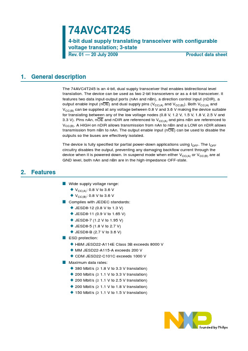
74AVC4T245 4位数据双向电平转换IC
terminal 1 index area
1DIR 2 2DIR 3 1A1 4 1A2 5 2A1 6 2A2 7
GND(1)
15 1OE 14 2OE 13 1B1 12 1B2 11 2B1 10 2B2
GND 8 GND 9
001aak284
Transparent top view
(1) The die substrate is attached to this pad using conductive die attach material. It cannot be used as a supply pin or input.
2B2, 2B1 10, 11
1B2, 1B1 12, 13
2OE, 1OE 14, 15
VCC(B)
16
Description supply voltage A (nAn, nOE and nDIR inputs are referenced to VCC(A)) direction control data input or output data input or output ground (0 V) data input or output data input or output output enable input (active LOW) supply voltage B (nBn inputs are referenced to VCC(B))
Fig 5. Pin configuration SOT763-1 (DHVQFN16)
5.2 Pin description
Table 2. Pin description
Symbol
Pin
VCC(A)
SN74AVC16T245中文资料

元器件交易网元器件交易网元器件交易网IMPORTANT NOTICETexas Instruments Incorporated and its subsidiaries (TI) reserve the right to make corrections, modifications,enhancements, improvements, and other changes to its products and services at any time and to discontinueany product or service without notice. Customers should obtain the latest relevant information before placingorders and should verify that such information is current and complete. All products are sold subject to TI’s termsand conditions of sale supplied at the time of order acknowledgment.TI warrants performance of its hardware products to the specifications applicable at the time of sale inaccordance with TI’s standard warranty. T esting and other quality control techniques are used to the extent TIdeems necessary to support this warranty. Except where mandated by government requirements, testing of allparameters of each product is not necessarily performed.TI assumes no liability for applications assistance or customer product design. Customers are responsible fortheir products and applications using TI components. T o minimize the risks associated with customer productsand applications, customers should provide adequate design and operating safeguards.TI does not warrant or represent that any license, either express or implied, is granted under any TI patent right,copyright, mask work right, or other TI intellectual property right relating to any combination, machine, or processin which TI products or services are used. Information published by TI regarding third-party products or servicesdoes not constitute a license from TI to use such products or services or a warranty or endorsement thereof.Use of such information may require a license from a third party under the patents or other intellectual propertyof the third party, or a license from TI under the patents or other intellectual property of TI.Reproduction of information in TI data books or data sheets is permissible only if reproduction is withoutalteration and is accompanied by all associated warranties, conditions, limitations, and notices. Reproductionof this information with alteration is an unfair and deceptive business practice. TI is not responsible or liable forsuch altered documentation.Resale of TI products or services with statements different from or beyond the parameters stated by TI for thatproduct or service voids all express and any implied warranties for the associated TI product or service andis an unfair and deceptive business practice. TI is not responsible or liable for any such statements.Following are URLs where you can obtain information on other Texas Instruments products and applicationsolutions:Products ApplicationsAmplifiers Audio /audioData Converters Automotive /automotiveDSP Broadband /broadbandInterface Digital Control /digitalcontrolLogic Military /militaryPower Mgmt Optical Networking /opticalnetworkMicrocontrollers Security /securityTelephony /telephonyVideo & Imaging /videoWireless /wirelessMailing Address:Texas InstrumentsPost Office Box 655303 Dallas, Texas 75265Copyright 2004, Texas Instruments Incorporated。
电压电平转换
SN74LVCC4245A
汽车类具有 5V 容限电平的 20 位 FET 2.5V/3.3V 低电压总线开关 具有 5V 容限电平转换器的 24 位 FET 2.5V/3.3V 低电压总线开关 24 位 FET 总线交换器,具有 5V 容限电平 转换器的 2.5V/3.3V 低电压总线开关 具有电平转换功能的单路 FET 总线开关
ACTIVE
MMC 和 SD 卡电压转换收发器
ACTIVE
MMC、SD 卡、记忆棒 (Memory Stick) 电压 转换收发器
ACTIVE
具有可配置电压转换和 3 态输出的 16 位双 电 具源 有总 可线 配收 置发 电器 压转换的 16 位双电源总线收 发 16器位双电源总线收发器,具有可配置 转换 和三态输出
ACTIVE ACTIVE ACTIVE
汽车类 16 位双电源总线收发器
ACTIVE
具有可配置电压转换和三态输出的 32 位双 电源总线收发器
ACTIVE
16 位双电源总线收发器,具有可配置 电压 转换和三态输出
ACTIVE
具有可配置电压转换和 电源总线收发器
3
态输出的
32
位双
ACTIVE
具有可配置电压转换和 源总线收发器
3
态输出的单位双电
ACTIVE
具有可配置电压转换和 源总线收发器
3
态输出的双位双电
ACTIVE
具有可配置电压转换和 3 态输出的 4 位双 电源总线收发器
ACTIVE
增强型产品 4 位双电源总线收发器, 具有 HiRel
可配置电压转换 和三态输出
ACTIVE
具有可配置电压转换和 3 态输出的 8 位双 电源总线收发器
车规的i2c电平转换芯片
车规的i2c电平转换芯片
以下是一些常见的车规级I2C 电平转换芯片:
1. Texas Instruments (TI) 的SN74LVC125A:这是一款具有低电压、高速特性的I2C 电平转换芯片,适用于汽车应用。
2. NXP Semiconductors 的PCA9509:这是一款低功耗、高速的I2C 和SPI 电平转换芯片,符合汽车级标准。
3. Microchip Technology 的MCP2221A:这是一款具有低功耗、高数据速率的I2C 电平转换芯片,适用于汽车和工业应用。
4. STMicroelectronics 的STM32F103C8T6:这是一款基于Arm Cortex-M3 内核的微控制器,内置I2C 接口,适用于汽车电子应用。
这些芯片通常具有低功耗、高抗扰性、宽工作温度范围等特点,以满足汽车环境的要求。
请注意,具体选择应根据你的应用需求、设计要求和供应商的可靠性等因素进行综合考虑。
在选择车规级芯片时,建议参考相关的汽车电子标准和规范,并与芯片供应商确认其是否符合车规要求。
双向电平转换芯片

双向电平转换芯片双向电平转换芯片又被称为双向电平转换器,是一种常用于电子电路中的集成电路芯片。
它主要用于将信号从一种逻辑电平转换为另一种逻辑电平,以实现不同电平之间的转换和适配。
双向电平转换器通常被应用于数字电路中,用于连接不同电平的数字设备,比如将5V的信号转换为3.3V的信号或将3.3V 的信号转换为5V的信号。
它可以使不同电平的设备能够互相通信和交换信息,从而实现数字电路的互联互通。
双向电平转换芯片一般由两个电平转换器和一个方向控制器组成,其中每个电平转换器有一个输入和一个输出,方向控制器用于控制输入和输出之间的通路。
当方向控制器的控制信号为高电平时,输入信号可以传递给输出,从而实现双向传输;当控制信号为低电平时,输入和输出之间的通路被切断,实现单向传输。
双向电平转换器的工作原理是通过使用电平转换器和方向控制器之间的逻辑电路来实现的。
电平转换器一般采用电平转换电路,通过改变输入电平的功耗,使输出电平达到预期的电压差值。
方向控制器通过控制输入和输出之间的通路的开闭状态,实现输入和输出之间的切换。
双向电平转换芯片具有以下优点和应用特点:1. 适应性强:双向电平转换芯片可以适应多种不同电平的设备和电路,可以将不同电平之间的信号进行转换和适配。
2. 高效性能:双向电平转换芯片具有快速响应速度和高精度的信号转换能力,使得不同电平设备之间的通信更加稳定和可靠。
3. 低功耗:双向电平转换芯片采用了先进的CMOS技术,功耗较低,可以有效降低系统能耗。
4. 多种封装形式:双向电平转换芯片可以采用多种不同的封装形式,如DIP、SOP、QFN等,方便 PCB 设计和布局。
5. 广泛应用:双向电平转换芯片广泛应用于各种数字电路中,如传感器、存储器、通信设备、嵌入式系统等。
总之,双向电平转换芯片是一种常用的集成电路芯片,用于不同电平设备之间的信号转换和适配。
它具有适应性强、高效性能、低功耗、多种封装形式等优点,并广泛应用于各种数字电路中。
一种解决贴片机贴装 IC 封装类型受限制的经济型措施
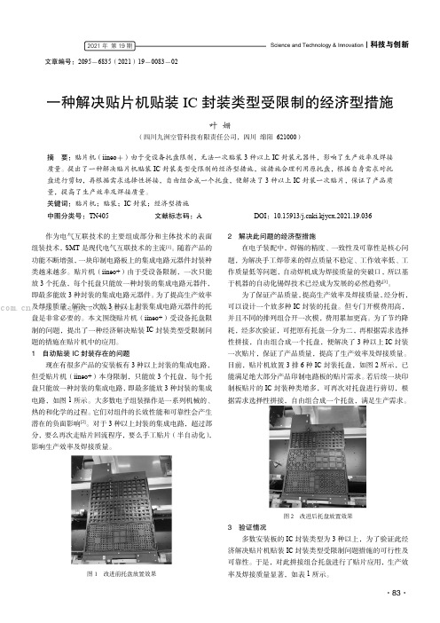
Science and Technology &Innovation ┃科技与创新2021年第19期·83·文章编号:2095-6835(2021)19-0083-02一种解决贴片机贴装IC 封装类型受限制的经济型措施叶姗(四川九洲空管科技有限责任公司,四川绵阳621000)摘要:贴片机(iineo +)由于受设备托盘限制,无法一次贴装3种以上IC 封装元器件,影响了生产效率及焊接质量。
提出了一种解决贴片机贴装IC 封装类型受限制的经济型措施,该措施合理利用原托盘,根据自身需求对托盘进行剪切,再根据需求选择性拼接,自由组合成一个托盘,便解决了3种以上IC 封装一次贴片,保证了产品质量,提高了生产效率及焊接质量。
关键词:贴片机;贴装;IC 封装;经济型措施中图分类号:TN405文献标志码:ADOI :10.15913/ki.kjycx.2021.19.036作为电气互联技术的主要组成部分和主体技术的表面组装技术,SMT 是现代电气互联技术的主流[1]。
随着产品的功能不断增强,一块印制电路板上的集成电路元器件封装种类越来越多。
贴片机(iineo+)由于受设备限制,一次只能放3个托盘,每个托盘只能放一种封装的集成电路元器件,即最多能放3种封装的集成电路元器件。
为了提高生产效率及焊接质量,解决一次放3种以上封装集成电路元器件的托盘是非常必要的。
本文围绕贴片机(iineo+)受设备托盘限制的问题,提出了一种经济解决贴装IC 封装类型受限制问题的措施在贴片机中的应用。
1自动贴装IC 封装存在的问题现在有很多产品的安装板有3种以上封装的集成电路,但受贴片机(iineo+)本身限制,只能放3个托盘,每个托盘只能放一种封装的集成电路,即最多能放3种封装的集成电路,如图1所示。
大多数电子组装操作是一系列机械的、热的和化学的过程。
它们对组件的长效性能和可靠性会产生潜在的负面影响[2]。
对于3种以上封装的集成电路,超过部分,要么再次走贴片回流程序,要么手工贴片(半自动化),影响生产效率及焊接质量。
电平转换SN74HCT245N-datasheet

PACKAGING INFORMATIONAddendum-Page 1Addendum-Page 2(1) The marketing status values are defined as follows:ACTIVE: Product device recommended for new designs.LIFEBUY: TI has announced that the device will be discontinued, and a lifetime-buy period is in effect.NRND: Not recommended for new designs. Device is in production to support existing customers, but TI does not recommend using this part in a new design.PREVIEW: Device has been announced but is not in production. Samples may or may not be available.OBSOLETE: TI has discontinued the production of the device.(2) Eco Plan - The planned eco-friendly classification: Pb-Free (RoHS), Pb-Free (RoHS Exempt), or Green (RoHS & no Sb/Br) - please check /productcontent for the latest availability information and additional product content details.TBD: The Pb-Free/Green conversion plan has not been defined.Pb-Free (RoHS): TI's terms "Lead-Free" or "Pb-Free" mean semiconductor products that are compatible with the current RoHS requirements for all 6 substances, including the requirement that lead not exceed 0.1% by weight in homogeneous materials. Where designed to be soldered at high temperatures, TI Pb-Free products are suitable for use in specified lead-free processes.Pb-Free (RoHS Exempt): This component has a RoHS exemption for either 1) lead-based flip-chip solder bumps used between the die and package, or 2) lead-based die adhesive used between the die and leadframe. The component is otherwise considered Pb-Free (RoHS compatible) as defined above.Green (RoHS & no Sb/Br): TI defines "Green" to mean Pb-Free (RoHS compatible), and free of Bromine (Br) and Antimony (Sb) based flame retardants (Br or Sb do not exceed 0.1% by weight in homogeneous material)(3) MSL, Peak Temp. - The Moisture Sensitivity Level rating according to the JEDEC industry standard classifications, and peak solder temperature.(4) There may be additional marking, which relates to the logo, the lot trace code information, or the environmental category on the device.(5) Multiple Device Markings will be inside parentheses. Only one Device Marking contained in parentheses and separated by a "~" will appear on a device. If a line is indented then it is a continuation of the previous line and the two combined represent the entire Device Marking for that device.(6) Lead/Ball Finish - Orderable Devices may have multiple material finish options. Finish options are separated by a vertical ruled line. Lead/Ball Finish values may wrap to two lines if the finish value exceeds the maximum column width.Important Information and Disclaimer:The information provided on this page represents TI's knowledge and belief as of the date that it is provided. TI bases its knowledge and belief on information provided by third parties, and makes no representation or warranty as to the accuracy of such information. Efforts are underway to better integrate information from third parties. TI has taken and continues to take reasonable steps to provide representative and accurate information but may not have conducted destructive testing or chemical analysis on incoming materials and chemicals. TI and TI suppliers consider certain information to be proprietary, and thus CAS numbers and other limited information may not be available for release.Addendum-Page 3In no event shall TI's liability arising out of such information exceed the total purchase price of the TI part(s) at issue in this document sold by TI to Customer on an annual basis.OTHER QUALIFIED VERSIONS OF SN54HCT245, SN54HCT245-SP, SN74HCT245 :•Catalog: SN74HCT245, SN54HCT245•Military: SN54HCT245•Space: SN54HCT245-SPNOTE: Qualified Version Definitions:•Catalog - TI's standard catalog product•Military - QML certified for Military and Defense Applications•Space - Radiation tolerant, ceramic packaging and qualified for use in Space-based applicationAddendum-Page 4TAPE AND REELINFORMATION*Alldimensions are nominalDevicePackage Type Package Drawing Pins SPQReel Diameter (mm)Reel Width W1(mm)A0(mm)B0(mm)K0(mm)P1(mm)W (mm)Pin1Quadrant SN74HCT245DBR SSOP DB 202000330.016.48.27.5 2.512.016.0Q1SN74HCT245DWR SOIC DW 202000330.024.410.813.3 2.712.024.0Q1SN74HCT245NSR SO NS 202000330.024.48.213.0 2.512.024.0Q1SN74HCT245PWR TSSOP PW 202000330.016.4 6.957.1 1.68.016.0Q1SN74HCT245PWTTSSOPPW20250330.016.46.957.11.68.016.0Q1PACKAGE MATERIALS INFORMATION1-Jul-2013Pack Materials-Page 1*All dimensionsare nominal DevicePackage Type Package Drawing Pins SPQ Length (mm)Width (mm)Height (mm)SN74HCT245DBRSSOP DB 202000367.0367.038.0SN74HCT245DWRSOIC DW 202000367.0367.045.0SN74HCT245NSRSO NS 202000367.0367.045.0SN74HCT245PWRTSSOP PW 202000364.0364.027.0SN74HCT245PWT TSSOP PW 20250367.0367.038.0PACKAGE MATERIALS INFORMATION 1-Jul-2013Pack Materials-Page 2IMPORTANT NOTICETexas Instruments Incorporated and its subsidiaries(TI)reserve the right to make corrections,enhancements,improvements and other changes to its semiconductor products and services per JESD46,latest issue,and to discontinue any product or service per JESD48,latest issue.Buyers should obtain the latest relevant information before placing orders and should verify that such information is current and complete.All semiconductor products(also referred to herein as“components”)are sold subject to TI’s terms and conditions of sale supplied at the time of order acknowledgment.TI warrants performance of its components to the specifications applicable at the time of sale,in accordance with the warranty in TI’s terms and conditions of sale of semiconductor products.Testing and other quality control techniques are used to the extent TI deems necessary to support this warranty.Except where mandated by applicable law,testing of all parameters of each component is not necessarily performed.TI assumes no liability for applications assistance or the design of Buyers’products.Buyers are responsible for their products and applications using TI components.To minimize the risks associated with Buyers’products and applications,Buyers should provide adequate design and operating safeguards.TI does not warrant or represent that any license,either express or implied,is granted under any patent right,copyright,mask work right,or other intellectual property right relating to any combination,machine,or process in which TI components or services are rmation published by TI regarding third-party products or services does not constitute a license to use such products or services or a warranty or endorsement e of such information may require a license from a third party under the patents or other intellectual property of the third party,or a license from TI under the patents or other intellectual property of TI.Reproduction of significant portions of TI information in TI data books or data sheets is permissible only if reproduction is without alteration and is accompanied by all associated warranties,conditions,limitations,and notices.TI is not responsible or liable for such altered rmation of third parties may be subject to additional restrictions.Resale of TI components or services with statements different from or beyond the parameters stated by TI for that component or service voids all express and any implied warranties for the associated TI component or service and is an unfair and deceptive business practice. TI is not responsible or liable for any such statements.Buyer acknowledges and agrees that it is solely responsible for compliance with all legal,regulatory and safety-related requirements concerning its products,and any use of TI components in its applications,notwithstanding any applications-related information or support that may be provided by TI.Buyer represents and agrees that it has all the necessary expertise to create and implement safeguards which anticipate dangerous consequences of failures,monitor failures and their consequences,lessen the likelihood of failures that might cause harm and take appropriate remedial actions.Buyer will fully indemnify TI and its representatives against any damages arising out of the use of any TI components in safety-critical applications.In some cases,TI components may be promoted specifically to facilitate safety-related applications.With such components,TI’s goal is to help enable customers to design and create their own end-product solutions that meet applicable functional safety standards and requirements.Nonetheless,such components are subject to these terms.No TI components are authorized for use in FDA Class III(or similar life-critical medical equipment)unless authorized officers of the parties have executed a special agreement specifically governing such use.Only those TI components which TI has specifically designated as military grade or“enhanced plastic”are designed and intended for use in military/aerospace applications or environments.Buyer acknowledges and agrees that any military or aerospace use of TI components which have not been so designated is solely at the Buyer's risk,and that Buyer is solely responsible for compliance with all legal and regulatory requirements in connection with such use.TI has specifically designated certain components as meeting ISO/TS16949requirements,mainly for automotive use.In any case of use of non-designated products,TI will not be responsible for any failure to meet ISO/TS16949.Products ApplicationsAudio /audio Automotive and Transportation /automotiveAmplifiers Communications and Telecom /communicationsData Converters Computers and Peripherals /computersDLP®Products Consumer Electronics /consumer-appsDSP Energy and Lighting /energyClocks and Timers /clocks Industrial /industrialInterface Medical /medicalLogic Security /securityPower Mgmt Space,Avionics and Defense /space-avionics-defense Microcontrollers Video and Imaging /videoRFID OMAP Applications Processors /omap TI E2E Community Wireless Connectivity /wirelessconnectivityMailing Address:Texas Instruments,Post Office Box655303,Dallas,Texas75265Copyright©2013,Texas Instruments Incorporated。
sn74hc165dr工作原理

sn74hc165dr工作原理SN74HC165DR是一种串行输入、并行输出的移位寄存器,它具有广泛的应用领域。
本文将介绍SN74HC165DR的工作原理及其应用。
SN74HC165DR采用了串行-并行转换的方式,可以将串行输入的数据转换为并行输出。
它具有8个输入引脚(D0-D7)、1个时钟引脚(CLK)、1个使能引脚(OE)、1个清除引脚(CLR)和8个并行输出引脚(Q0-Q7)。
当使能引脚(OE)为低电平时,SN74HC165DR处于使能状态,可以正常工作。
当时钟引脚(CLK)上出现上升沿时,SN74HC165DR会将串行输入引脚(D0-D7)上的数据按照从低位到高位的顺序依次输入,并将其存储在内部的8位移位寄存器中。
移位寄存器可以看作是一个存储数据的缓存器,它的作用是将串行输入的数据进行存储和转换。
当时钟引脚上出现8个上升沿时,SN74HC165DR将通过并行输出引脚(Q0-Q7)将移位寄存器中的数据并行输出。
每个并行输出引脚对应一个位的数据,可以将其连接到其他器件或电路中进行进一步的处理。
在使用SN74HC165DR时,可以通过使能引脚(OE)控制使能状态,通过时钟引脚(CLK)控制数据输入和输出的时机,通过串行输入引脚(D0-D7)输入待转换的数据,通过并行输出引脚(Q0-Q7)输出转换后的数据。
SN74HC165DR的工作原理简单明了,它可以方便地将串行输入的数据转换为并行输出。
这种转换方式在许多应用场景中都非常有用。
例如,在数字电子系统中,可以使用SN74HC165DR将外部输入的数字信号转换为并行数据,然后再进行处理和分析。
在工业自动化控制系统中,可以使用SN74HC165DR将输入的开关信号转换为并行数据,以实现对设备的控制。
SN74HC165DR是一种功能强大的移位寄存器,它可以实现串行输入、并行输出的数据转换。
通过控制使能引脚和时钟引脚,可以灵活地控制数据的输入和输出时机。
74HC165中文资料-数据手册-参数
74HC165中文资料数据手册参数一、74HC165简介1. 工作电压范围宽:2.0V至6.0V;2. 工作频率高:最高可达50MHz;3. 低功耗:静态功耗几乎为零;4. 输入输出兼容TTL电平;5. 封装形式多样:DIP、SOIC、TSSOP等。
二、74HC165参数1. 电源电压(VCC):2.0V至6.0V;2. 输入电压(VIN):0V至VCC;3. 输出电压(VOUT):0V至VCC;4. 工作温度范围:40℃至+125℃;5. 最大输入电流(II):±1μA;6. 最大输出电流(IO):±25mA;7. 最大功耗(PD):500mW(TA=25℃);8. 传输延迟时间(tpd):22ns(典型值,VCC=5V);9. 输入上升时间(tr):20ns(典型值,VCC=5V);10. 输入下降时间(tf):20ns(典型值,VCC=5V);11. 输出上升时间(tr):25ns(典型值,VCC=5V);12. 输出下降时间(tf):25ns(典型值,VCC=5V)。
三、74HC165引脚功能1. AH(输入端):8位并行数据输入端;2. SH/LD(移位/装载控制端):高电平时,数据从输入端AH并行装载到寄存器;低电平时,数据从输入端A串行移位进入寄存器;3. CLK(时钟输入端):上升沿触发,用于控制数据的移位和装载;4. SER(串行输入端):串行数据输入端,用于接收外部串行数据;5. QH'(串行输出端):串行数据输出端,输出最高位;6. GND(地):电源地;7. VCC(电源):正电源输入。
四、74HC165应用电路1. 数据串行化:将并行数据转换为串行数据,以便于通过单线或少量线进行传输。
2. 数据扩展:通过级联多个74HC165,实现数据位数的扩展,增加并行数据的宽度。
3. 数据缓冲:作为数据缓冲器,提高系统的驱动能力。
【电路图】将74HC165的AH端连接至并行数据源;SH/LD端接高电平,使能并行数据装载;CLK端接时钟信号,控制数据装载和移位;SER端接下一级74HC165的QH'端,实现级联;QH'端输出串行数据至下一级处理或传输。
常用电平转换芯片

常用电平转换芯片芯片描述电压范围位数是否双电源SN74AVC1T45 具有可配置电压转换和 3 态输出的单位双电源总线收发器 1.2 3.6 两者兼有 1 双电源SN74LVC1T45 具有可配置电压转换和 3 态输出的单位双电源总线收发器 1.65 5.5 两者兼有 1 双电源SN74AVCH2T45 具有可配置电压转换和 3 态输出的双位双电源总线收发器 1.2 3.6 两者兼有 2 双电源SN74LVC2T45 具有可配置电压转换和 3 态输出的双位双电源收发器 1.65 5.5 两者兼有 2 双电源SN74AVC2T45 具有可配置电压转换和 3 态输出的双位双电源总线收发器 1.2 3.6 两者兼有 2 双电源SN74AVCH4T245 具有可配置电压转换和 3 态输出的 4 位双电源总线收发器 1.2 3.6 两者兼有 4 双电源SN74AVC4T245 具有可配置电压转换和 3 态输出的 4 位双电源总线收发器 1.2 3.6 两者兼有 4 双电源SN74AVCH8T245 具有可配置电压转换和 3 态输出的 8 位双电源总线收发器 1.2 3.6 两者兼有 8 双电源SN74LVC8T245 具有可配置电压转换和 3 态输出的 8 位双电源总线收发器 1.65 5.5 两者兼有 8 双电源SN74AVC8T245 具有可配置电压转换和 3 态输出的 8 位双电源总线收发器 1.2 3.6 两者兼有 8 双电源SN74LVC16T245 具有可配置电压转换和 3 态输出的 16 位双电源总线收发器 1.65 5.5 两者兼有 16 双电源SN74AVC16T245 具有可配置电压转换和 3 态输出的 16 位双电源总线收发器 1.2 3.6 两者兼有 16 双电源SN74AVC20T245 具有可配置电压转换和 3 态输出的 20 位双电源总线收发器 1.2 3.6 两者兼有 20 双电源SN74AVC24T245 具有可配置电压转换和 3 态输出的 24 位双电源总线收发器 1.2 3.6 两者兼有 24 双电源SN74AVC32T245 具有可配置电压转换和 3 态输出的 32 位双电源总线收发器 1.2 3.6 两者兼有 32 双电源SN74TVC3306 双路钳位电压 0.8 5.0 两者兼有 2 FET 开关SN74TVC3010 10 位钳位电压 0.8 5.0 两者兼有 10 FET 开关SN74TVC16222A 22 位钳位电压 0.8 5.0 两者兼有 22 FET 开关。
5v和3.3v芯片互转

3.3v和5v双向电平转换芯片74LVC4245,8位电平转换74LVC4245A,8位双向NLSX4373,2位电平转换NLSX4014,4位电平转换NLSX4378,4位电平转换NLSX3018,8位电平转换max3002,8路双向TXB0104?(她好像有一个系列?0102?0104?0106?0108),ADG330874HCT245:三态输出的八路总线收发器SN74A VCH2T45SN74A VC16T245:具有可配置电压转换和 3 态输出的16 位双电源总线收发器SN74LVC2T45DCT:双位双电源总线收发器可配置电压转换和三态输出SN74LVC4245A:8位德州仪器宣布推出SN74LVC1T45、SN74LVC2T45、SN74A VC8T245及SN74A VC20T245四款新型双电源电平转换收发器。
该新品能够在 1.5V、1.8V、2.5V、3.3V 与5V 电压节点之间进行灵活的双向电平转换,而且可提供全面的可配置性。
如果采用A VC 技术,则每条轨可从1.4V 配置为3.6V;而采用LVC 技术时则可从 1.65V 配置为5.5V。
适用于便携式消费类电子产品、网络、数据通信以及计算应用领域。
日前,德州仪器(TI)宣布推出四款新型的双电源电平转换器--A VC1T45、A VC2T45、A VC16T245及A VC32T245,从而进一步扩展其电平转换产品系列。
这些转换器能够在互不兼容的I/O之间进行通信。
这四款器件均支持1.2V、1.5V、1.8V、2.5V与3.3V节点之间的双向电平转换。
在混合信号环境中,可以使用这些电压电平的任意组合,从而提高这些器件的灵活性。
1位A VC1T45与2位A VC2T45可根据需要在电路板上集成单或双转换器功能,而不是通过较高位宽的器件进行路由,这有助于简化电路板布线作业(board routing),可适用于便携式手持应用的转换要求。
- 1、下载文档前请自行甄别文档内容的完整性,平台不提供额外的编辑、内容补充、找答案等附加服务。
- 2、"仅部分预览"的文档,不可在线预览部分如存在完整性等问题,可反馈申请退款(可完整预览的文档不适用该条件!)。
- 3、如文档侵犯您的权益,请联系客服反馈,我们会尽快为您处理(人工客服工作时间:9:00-18:30)。
θJA
Package thermal impedance(4)
Tstg Storage temperature range
I/O ports (A port) I/O ports (B port) Control inputs A port B port A port B port VI < 0 VO < 0
Absolute Maximum Ratings(1)
over operating free-air temperature range (unless otherwise noted)
VCCA VCCB
Supply voltage range
VI
Input voltage range(2)
VO
Voltage range applied to any output in the high-impedance or power-off state(2)
PRODUCTION DATA information is current as of publication date. Products conform to specifications per the terms of the Texas Instruments standard warranty. Production processing does not necessarily include testing of all parameters.
VO
Voltage range applied to any output in the high or low state(2)(3)
IIK
Input clamp current
IOK
Output clamp current
IO
Continuous output current
Continuous current through each VCCA, VCCB, and GND
SN74AVC16T245 16-BIT DUAL-SUPPLY BUS TRANSCEIVER WITH CONFIGURABLE VOLTAGE TRANSLATION AND 3-STATE OUTPUTS
SCES551C – FEBRUARY 2004 – REVISED AUGUST 2005
Copyright © 2004–2005, Texas Instruments Incorporated
SN74AVC16T245 16-BIT DUAL-SUPPLY BUS TRANSCEIVER WITH CONFIGURABLE VOLTAGE TRANSLATION AND 3-STATE OUTPUTS
The SN74AVC16T245 is designed so that the control pins (1DIR, 2DIR, 1OE, and 2OE) are supplied by VCCA.
ORDERING INFORMATION
TA
PACKAGE (1)
ORDERABLE PART NUMBER
FEATURES
• Control Inputs VIH/VIL Levels Are Referenced to VCCA Voltage
• VCC Isolation Feature – If Either VCC Input Is at GND, Both Ports Are in the High-Impedance State
The VCC isolation feature ensures that if either VCC input is at GND, both ports are in the high-impedance state.
To ensure the high-impedance state during power up or power down, OE should be tied to VCC through a pullup resistor; the minimum value of the resistor is determined by the current-sinking capability of the driver.
The SN74AVC16T245 is designed for asynchronous communication between data buses. The device transmits data from the A bus to the B bus or from the B bus to the A bus, depending on the logic level at the direction-control (DIR) input. The output-enable (OE) input can be used to disable the outputs so the buses effectively are isolated.
SCES551C – FEBRUARY 2004 – REVISED AUGUST 2005
LOGIC DIAGRAM (POSITIVE LOGIC)
24 2DIR
48 1OE
25 2OE
36 2A1
2 1B1
13 2B1
To Seven Other Channels
To Seven Other Channels
GQL OR ZQL PACKAGE (TOP VIEW)
123456
A B C D E F G H J K
TERMINAL ASSIGNMENTS(2)
1
2
A
1DIR
NC
B
1B2
1B1
C
1B4
1B3
D
1B6
1B5
E
1B8
1B7
F
2B1
2B2
G
2B3
2B4
H
2B5
2B6
J
2B7
2B8
K
2DIR
NC
(2) NC – No internal connection
TOP-SIDE MARKING AVC16T245 WF245
WF245
(1) Package drawings, standard packing quantities, thermal data, symbolization, and PCB design guidelines are available at /sc/package.
– 8000-V Human-Body Model (A114-A)
– 200-V Machine Model (A115-A)
– 1000-V Charged-Device Model (C101)
DESCRIPTION/ORDERING INFORMATION
This 16-bit noninverting bus transceiver uses two separate configurable power-supply rails. The SN74AVC16T245 is optimized to operate with VCCA/VCCB set at 1.4 V to 3.6 V. It is operational with VCCA/VCCB as low as 1.2 V. The A port is designed to track VCCA. VCCA accepts any supply voltage from 1.2 V to 3.6 V. The B port is designed to track VCCB. VCCB accepts any supply voltage from 1.2 V to 3.6 V. This allows for universal low-voltage bidirectional translation between any of the 1.2-V, 1.5-V, 1.8-V, 2.5-V, and 3.3-V voltage nodes.
• Ioff Supports Partial-Power-Down Mode Operation
• I/Os Are 4.6-V Tolerant
• Latch-Up Performance Exceeds 100 mA Per JESD 78, Class II
• ESD Protection Exceeds JESD 22
48 1OE 47 1A1 46 1A2 45 GND 44 1A3 43 1A4 42 VCCA 41 1A5 40 1A6 39 GND 38 1A7 37 1A8 36 2A1 35 2A2 34 GND 33 2A3 32 2A4 31 VCCA 30 2A5 29 2A6 28 GND 27 2A7 26 2A8 25 2OE
DGG OR DGV PACKAGE (TOP VIEW)
1DIR 1 1B1 2 1B2 3 GND 4 1B3 5 1B4 6 VCCB 7 1B5 8 1B6 9 GND 10 1B7 11 1B8 12 2B1 13 2B2 14 GND 15 2B3 16 2B4 17 VCCB 18 2B5 19 2B6 20 GND 21 2B7 22 2B8 23 2DIR 24
INPUTS
OE DIR
L
L
L
H
H
X
OPERATION
B data to A bus A data to B bus
Isolation
2
1DIR 1
1A1 47
SN74AVC16T245 16-BIT DUAL-SUPPLY BUS TRANSCEIVER WITH CONFIGURABLE VOLTAGE TRANSLATION AND 3-STATE OUTPUTS