FMS6502中文资料
(国内标准)FMS实训教学指导书
(国内标准)FMS实训教学指导书实训教学指导书机电一体化柔性装配系统PLC控制天津市龙洲科技仪器有限公司目录机电一体化柔性装配系统概述 (1)第一单元上料单元 (5)一、单元简介 (5)二、实训目的 (7)三、实训设备 (7)四、实训内容与步骤 (8)五、控制要求 (9)六、I/O编号分配表 (14)第二单元下料单元 (16)七、单元简介 (16)八、实训目的 (18)九、实训设备 (18)十、实训内容与步骤 (18)十一、控制要求 (19)十二、I/O编号分配表 (22)第三单元加盖单元 (24)一、单元简介 (24)二、实训目的 (25)三、实训设备 (25)四、实训内容与步骤 (26)五、控制要求 (27)六、I/O编号分配表 (29)第四单元穿销单元 (31)一、单元简介 (31)二、实训目的 (32)三、实训设备 (32)四、实训内容与步骤 (32)五、控制要求 (34)六、I/O编号分配表 (36)第五单元模拟单元 (38)一、单元简介 (38)二、实训目的 (39)三、实训设备 (39)四、实训内容与步骤 (39)五、控制要求 (40)六、I/O编号分配表 (42)第六单元图像识别单元 (44)一、单元简介 (44)二、实训目的 (45)三、实训设备 (45)四、实训内容与步骤 (45)五、控制要求 (46)六、I/O编号分配表 (48)第七单元伸缩换向单元 (50)一、单元简介 (50)二、实训目的 (52)三、实训设备 (52)四、实训内容与步骤 (52)五、控制要求 (53)六、I/O编号分配表 (56)第八单元检测单元 (58)一、单元简介 (58)二、实训目的 (59)三、实训设备 (59)四、实训内容与步骤 (59)五、控制要求 (60)六、I/O编号分配表 (62)第九单元液压单元 (64)一、单元简介 (64)二、实训目的 (65)三、实训设备 (65)四、实训内容与步骤 (65)五、控制要求 (66)六、I/O编号分配表 (69)第十单元分拣单元 (71)二、实训目的 (72)三、实训设备 (72)四、实训内容与步骤 (72)五、控制要求 (73)六、I/O编号分配表 (77)第十一单元升降梯立体仓库单元 (79)一、单元简介 (79)二、实训目的 (83)三、实训设备 (83)四、实训内容与步骤 (83)五、控制要求 (85)六、I/O编号分配表 (91)第十二单元悬挂式高空搬运单元 (93)一、单元简介 (93)二、实训目的 (95)三、实训设备 (95)四、实训内容与步骤 (96)五、控制要求 (97)六、I/O编号分配表 (101)第十三单元传送单元 (103)一、转角单元 (103)第十四单元装配生产线全程连续控制 (105)一、实训目的 (105)二、实训设备 (105)三、实训内容与步骤 (105)四、控制要求 (108)五、系统全程控制中需注意的问题 (109)六、I/O编号分配表 (109)七、主站控制变量传送分配表 (109)附录 (111)附录1:上料单元电源系统图 (111)附录2:上料单元气动原理图 (112)附录3:上料单元PLC控制接线图 (113)附录4:下料单元电源系统图 (114)附录5:下料单元PLC控制接线图 (115)附录6:加盖单元电源系统图 (116)附录7:加盖单元PLC控制接线图 (117)附录8:穿销单元电源系统图 (118)附录9:穿销单元气动原理图 (119)附录10:穿销单元PLC控制接线图 (120)附录11:模拟单元电源系统图 (121)附录12:模拟单元气动原理图 (122)附录14:图像识别单元电源系统图 (124)附录15:图像识别单元PLC控制接线图 (125)附录16:伸缩换向单元电源系统图 (126)附录17:伸缩换向单元气动原理图 (127)附录18:伸缩换向单元PLC控制接线图 (128)附录19:检测单元电源系统图 (129)附录20:检测单元PLC控制接线图 (130)附录21:液压单元电源系统图 (131)附录22:液压单元油路原理图 (132)附录23:液压单元PLC控制接线图 (133)附录24:分拣单元电源系统图 (134)附录25:分拣单元气动原理图 (135)附录26:分拣单元PLC控制接线图 (136)附录27:升降梯立体仓库单元电源系统图 (137)附录28:升降梯立体仓库单元气动原理图 (138)附录29:升降梯立体仓库单元PLC控制接线图 (139)附录30:悬挂式高空搬运单元电源系统图 (140)附录31:悬挂式高空搬运单元PLC控制接线图 (141)附录32:电源系统总图 (143)附录33:电源系统用电分配图 (144)附录34:气路连接总图 (145)附录36:移动配电平台用户扩展接口分配图 (147)机电一体化柔性装配系统概述Me093399型机电一体化教学系统是以工业生产中的自动化装配生产线为原型开发的教学、实验、实训综合应用平台。
6502电气集中

第一章电气集中概述车站联锁设备是保证站内运输作业安全、提高作业效率的铁路信号设备,它的控制对象是道岔、进路和信号机。
将道岔、进路和信号机用电气方式集中控制与监督,并实现它们之间联锁关系的技术方法和设备称为电气集中联锁,用继电器实现联锁关系的称为继电式电气集中联锁(以下简称电气集中)。
6502电气集中是我国目前应用最普通的一种继电式电气集中联锁。
6502电气集中具有电路定型化程度高、逻辑性强,操作方法简便灵活、不易出错,维修、施工比较方便,符合故障—安全原则,易与区间闭塞设备及其他信号设备结合等优点;又是调度集中和调度监督的基础设备。
因此,在我国铁路得到了广泛应用。
第一节电气集中的组成电气集中分为室内设备和室外设备两大部分。
P1图1-1室内设有控制台、区段人工解锁按钮盘、继电器组合及组合架、电源屏、分线盘等设备。
室外设有色灯信号机、电动转辙机、轨道电路、电缆线路及电缆连接箱盒等设备。
第二节继电器组合及组合架一、继电器组合类型采用继电器定型组合的形式设计电路,不仅简化了设计,加快了设计过程,而且组合可在工厂预制,这就极大地缩短了施工工期。
6502电气集中的定型组合共有12种。
(一)信号组合类型LXZ、1LXF、2LXF、YX、DX、DXF(二)道岔组合类型DD、SDZ、SDF(三)区段组合类型Q(四)其他组合类型F、DY二、继电器组合的选用(一)进站信号机选用的组合1.在双线单向运行区段,每架进站信号机相应选用YX和LXZ两个组合。
2.在单线双向运行区段和双线双向运行区段,每架进站信号机应选择1LXF、YX、和LXZ三个组合。
3.当进站信号机内方有一无岔区段和同方向的调车信号机时,因为进站与调车信号机之间没有道岔,可作为一个信号点看待,一般称为进站内方带调车,可不设DX组合,仅选用1LXF、YX和LXZ三个定型组合,再增选一个零散组合(所谓零散组合就是根据具体情况设计的非定型组合)。
(二)出站兼调车信号机和发车进路信号机选用的组合1.当只有一个发车方向时,每架出站兼调车信号机应选用LXZ 和1LXF两个组合。
6502电气集中、64D半自动、控制台检修讲义004
6502电气集中学习课件
3、定型组合侧面电源规律 1)、一般情况下在LXZ、1LXF、YX、DY、Q、F、DX、DD、SDZ组
合侧面端子06-1、06-2为KZ24;06-3、06-4为KF24;06-5为 JZ;06-6为JF( DD、SDZ组合除外) 2)、 DD、SDZ组合侧面端子06-15为DZ220;06-16为DF220; 06-17为DJZ220;06-18为DJF220 3)、 LXZ、DX组合侧面端子06-17为XJZ220;06-18为XJF220
控制台学习课件
3、事故通知按钮的使用 1)、设备发生故障后,值班员按压事故通知按钮,故障信息经
微机监测的通道上传。 2)、信号到达该站后,点击微机监测界面弹出的方框,开始记
录故障处理的到达时间,故障处理起始时间。 3)、故障处理完毕后,到控制台拉出事故通知按钮,在回到机
械室点击微机监界面测弹出的方框,记录故障处理结束时间, 最后给事故通知按钮加封,消记。
个人署名
6502电气集中学习课件
7)、继电器动作示意图 (从左往右的进路)
排列表示灯亮,FJ励磁
LKJ FKJ
LKJ第一自闭
个人署名
控制台学习课件 二、控制台检修标准 1、按钮接点的接通和断开与按钮的按压、停留、复位的位置关系
正确,按钮在受振动时,接点不得错接或错断。 2、控制台各表示灯显示正确,无窜光现象,股道示意条完整清晰。 3、控制台内部配线整齐,端子无松动。 4、控制台内部电源无接地、漏流现象。 5、控制台各部安装稳固,不歪斜,防尘、防潮良好。 6、控制台加封加锁良好,计数器计数正确,不跳码,不漏码。 7、控制台的电源熔丝容量符合规定。KZ(3A)、KF(3A)、JZ(5A)、
GE综保F650中文简介

监视和测量故障测距、最后10次记录断路器跳闸和失灵VT 断线断路器总拉弧电流事件记录-479次事件高分辨率录波和数据记录,采样速率可编程设置测量:V ,I ,Hz ,W ,VA ,PF需量:Ia ,Ib ,Ic ,Ig ,Isg ,I2,MW ,MVA 可配置图形人机接口报警显示前面板配备往复键,4x20个字节的背光显示屏幕或16x40个字节的可选择的图形显示屏幕RS232和RS485接口-速率可达115,200 bps以太网接口-10/100BaseTX ,100BaseFX 带ST 接头,可选的带ST 接头的双100BaseFX ,用于物理介质冗余多规约-ModBus TM RTU 和TCP/IP DNP 3.0级别2,IEC 60870-5-104,IEC 61850,Http ,ftp 和tftpEnerVista 软件-处于工业系统领先地位的软件工具,与GE Multilin 设备一起使用,简化工作过程的每一个方面用户接口保护和控制完整的延时、瞬时和相方向、中性点、接地和灵敏接地过电流不同线路中的负序延时过流断线检测相延时过流的电压制动母线和线路辅助压欠压/过电压中性点过电压负序电压母线欠频率/过频率断路器失灵由PLC 控制的带冷负荷启动的手动合闸可配置的四次重合闸3个定值设置组同期检查-V ,φ和Hz 多达32个可编程数字输入多达16个数字输出跳闸回路监视冗余电源选择可编程逻辑高成本效益的信息访问-通过多规约、标准RS232、RS485和以太网端口通过开放式标准规约达到最佳化的集成灵活性-Modbus RTU 和TCP/IP ,DNP 3.0级别2,IEC 60870-5-104,IEC 61850与标准internet 浏览器兼容-通过规约,例如Http ,ftp 和tftp最大程度地缩短通讯中断时间-配备10/100BaseTX 的可靠冗余以太网通讯端口,100BaseFX 配备ST 接头,可选择的双100BaseFX 也配备ST 接头完备的监视功能-包括需量和电能在内的详尽测量功能跟随技术发展-用于产品现场升级的闪存技术独特的嵌入式控制功能-综合馈线保护加可编程逻辑对于复杂系统的灵活性和高成本效率的控制-使用符合IEC 标准的可编程逻辑自定义馈线保护和控制系统的功能,满足独特的要求一流的人机接口(HMI)-4 x 20标准背光式LCD 显示,可选择16 x 40(240x128像素)图形LCD ,配备可编程按钮和选择设置菜单及子菜单的旋转开关更换时间最小化-模块化设计,插件可抽出结构减少故障排除时间和降低维护成本-IRIG-B 时间同步、事件报告、波形捕捉、数据记录配电线路和母联的管理和主保护母线、变压器和输电线路的后备保护可靠的配电发电互联保护系统和中低压电动机保护主要优点馈线/间隔保护系统保护、控制、监视、分析和电能计量系统应用特性保护和控制F650提供用于馈线管理和间隔控制的快速保护和控制,保护功能包括:过流保护瞬时和延时过流功能可用于相、中性点、接地/灵敏接地,延时过流功能可用于负序电流。
(改)威步产品目录2011.03(1) ZLMICRO半导体品牌

Low ESR Caps Compatible High Speed LDO Voltage Regulators with ON/OFF Switch High Current, High Speed LDO Regulators 3A 150KHZ PWM Buck DC/DC Converter 2A 150KHZ PWM Buck DC/DC Converter Low-Power DC/DC Boost Converter In SOT-23 And Son Packages Multiple Voltage Regulator
EEPROM
K24C01 K24C02 K24C04 K24C08 K24C16 K24C32 K24C64
RDS解码
AT6588 AT6579 BU1924
锁相环
AT9256 AT9257 LC72131
LCD驱动
HL1621 ZL LP6578 ZL75823A ZL75823B ZL75823C ZL75824 Temp Sensor DS3501 新增产品 MP2259 MP2359DJ AD9943 TW2868 TW2867 ZLIA171 K24C256
step-up DC/DC converter is optimized for driving OLEDs or white LEDs inductor-based DC/DC boost converter designed to drive LED Arrays 1.3A Fixed Frequency White LED Driver 1.3A Fixed Frequency white LED Driver 3A, 28V, 385KHz Step-Down Converter 250mW Dual Channel Audio Power Amplifier With Shutdown 1 Watt Audio Power Amplifier Dual 2.2w Audio Amplifier Plus Stereo Headphone Function 1.1W Audio Power Amplifier With Shutdown Mode 5X5W Amplifier With DC Volume Control 2x6W Stereo Power Amplifier 4X35W Quad Bridge Car Radio Amplifier 4X45W Quad Bridge Car Radio Amplifier 4X41W Quad Bridge Car Radio Amplifier 4-Channel Audio Processor IC 4 channels sound effect processor 4 channels sound effect processor Car radio multimedia signal processor (CMSP) 3 Band Car Audio Processor 3 Band Car Audio Processor Car Audio Processor Sound Processor for car audio SigmaDSP® 28/56-Bit Audio Processor with 2ADC/4DAC SigmaDSP® 28/56-Bit Audio Processor with 2ADC/4DAC 3-Input Video Switch 3-Input Video Switch With 75Ω Driver 8-Input,6-Output Video Switch Matrix With Output Drivers,Input clamp,and Bias Circuitry 12-Input,9-Output Video Switch Matrix With Input clamp,Input Bias Circuitry,and Output Drivers 10-Bit, 4× Oversampling SDTV Video Decoder
6502使用说明详解

黔江站6502使用说明书第一章概述本说明书仅就黔江6502型大站电气集中的使用办法,作一简要说明,供行车人员参考。
电气集中设备包括有以下几个主要部分:一、室内设备1、控制台:是车站值班员办理行车作业和监督现场线路状态的主要设备。
2、组合继电器架:是构成信号与道岔互相联锁的主要设备。
3、电源部分:自动调压器、交流电源屏、直流电源屏。
由它们供给联锁设备、色灯信号机、轨道电路、电动转辙机、控制台上各种表示等电源。
4、人工解锁按钮盘:是设备发生故障,解锁区段用以及在维修中需要解锁区段时应用。
5、黔江站6502控制台如下图所示:二、室外部分:1、色灯信号机:指示列车和调车作业,根据色灯信号的显示进行或停止。
2、电动转辙机:装在道岔上,转换道岔用。
3、轨道电路:检查线路和道岔区段空闲或占用。
三、电气集中设备保证道岔和信号机间的相互联锁,并能保证以下条件:l、信号机在其防护的进路上的有关道岔开通位置不对或敌对信:号机未关闭时不能开放;信号机开放后,该进路上的有关道岔不能扳动,其敌对信号机不能开放。
2、与进站同方向的正线上的出站信:号机未开放时,进站色灯信号机的绿色灯光不能开放。
主体信号机未开放时,预告信号机不能开放。
3、在控制台上,能监督线路及道岔区段是否占用、进路开通方向、复示有关信号机的显示,监督是否挤岔,并于挤岔的同时使防护有关进路的信号机自行关闭。
4、当在道岔转辙连接杆处的尖轨与基本轨间插入厚4毫米,宽90毫米的铁板时,应不能锁闭和开放信号。
第二章色灯信号机类型及显示意义信号是指示列车运行及调车作业的命令,有关行车人员必须按信号指示办事。
信号平面图上色灯信号机的颜色图例:红色——停车;黄色——注意或减低速度;绿色——按规定速度运行;月白色——准许越过该信号机调车;蓝色——禁止越过该信号机调车。
—、进站、进路色灯信号机1、一个绿色灯光:准许列车按规定速度由正线通过车站;2,一个黄色灯光:准许列车进入站内正线停车;3、两个黄色灯光:准许列车进入站内到发线停车;4、一个绿色灯光和—个黄色灯光:准许列车进入站内停车,表示进路信号机在开放状态,出站信号机在关闭状;5、一个红色灯光:不准列车越过该信号机;6、引导信号显示一个红色灯光及一个月白色灯光:准许列车在该信号机前方不停车,以不道过20公里/小时速度进站或通过接车进路,并须准备能随时停车。
FMS6502_V1.0_
IN4 ADDR1
IN5 ADDR0
IN6 SCL
GND OUT1 OUT2 OUT3 VDD OUT4 OUT5 OUT6 GND IN8 SDA IN7
序号 13 14 15 16 17 18 19
符号 IN7 SDA IN8 GND OUT6 OUT5 OUT4
功能描述 输入通道 7 I 2 C 总线数据口 输入通道 8 地 输出通道 6 输出通道 5 输出通道 4
OUT5,6 0x02 B3-Out6 B2-Out6 B1-Out6 B0-Out6 B3-Out5 B2-Out5 B1-Out5 B0-Out5
Clamp 控制寄存器及默认值:
控制名称 Clmp
位宽 1 bit
类型 Write
默认值 0
位号
描述
7-0 Clamp / Bias 选择:1 = clamp,0 = Bias
ADDR1 0 0 1 1
ADDR0 0 1 0 1
Binary 0000 0110 0100 0110 1000 0110 1100 0110
Hex 0x06 0x46 0x86 0xc6
8 位的数据和地址数据写到 FMS6502 的 I2C 地址寄存器中,以选择控制功能。为了提高效率, 两个输出共用一个数据寄存器来进行输入选择。多个输出可以选择相同的输入通道,实现一进多出 切换。Clamp 和 bias 控制位写在它们自己的内部地址中,因为不管信号通道如何选择,Clamp 和 bias 控制位应保持相同。它们是根据连接到 FMS6502 上的输入信号来设置的。
V. 1.0
第 2 页 共 14 页
FMS6502
2 交流参数
TA = 25 ℃, VCC = 5 V, VIN = 1 VPP,输入偏置模式,单进单出切换,6 dB 增益,所有交流输入 加 0.1 µF,未使用的交流输入通过 75 Ω 线缆连接到地,所有的交流输出外加 220 µF 和 150 Ω 负载, 通常情况使用 400 kHz,除非另有特殊说明。
6502芯片

6502芯片6502芯片是一款8位微处理器芯片,由摩斯技术公司(MOS Technology)于1975年推出,并由苹果公司在1976年发布的Apple I计算机中使用。
6502芯片是当时市场上最便宜的微处理器之一,因此很受欢迎,被广泛应用于个人电脑、游戏机和其他各种电子设备中。
6502芯片的主要特点如下:1. 8位结构:6502芯片是一款8位微处理器,意味着它可以同时处理8位的数据。
每个字节可以存储8个二进制数字,范围从0到255。
2. 低功耗:6502芯片是基于MOS技术的,具有较低的功耗。
它采用了静态设计,只有在电压改变时才会消耗能量。
3. 低成本:6502芯片的制造成本较低,这是由于它的设计简单,特别注重经济性。
这使得6502芯片成为一种广泛应用于大众市场的处理器。
4. 低运行频率:6502芯片的最高时钟频率为1 MHz,比较低,但足够满足当时的计算需求。
5. 简化指令集:6502芯片具有一种精简的指令集架构,包括56条指令。
这些指令可以直接操作CPU寄存器和内存,加快了数据处理速度。
6. 易于编程:6502芯片使用汇编语言进行编程,汇编语言较为直接、简单,可以更好地控制和优化程序的执行。
6502芯片的应用广泛,特别是在个人电脑领域。
它被用于苹果公司的Apple II系列电脑、Atari游戏机、Commodore 64和BBC Micro等。
这些机器在当时非常受欢迎,为个人电脑的普及做出了重要贡献。
尽管6502芯片已经过时,但它仍然被一些人用于制作复古计算机和模拟器。
此外,6502的设计思想和部分指令集架构仍然影响着现代的微处理器设计。
总结起来,6502芯片是一款经典的8位微处理器芯片,具有低功耗、低成本和简化指令集等特点。
它对个人电脑的发展起到了重要的推动作用,并在当时广泛应用于各种电子设备中。
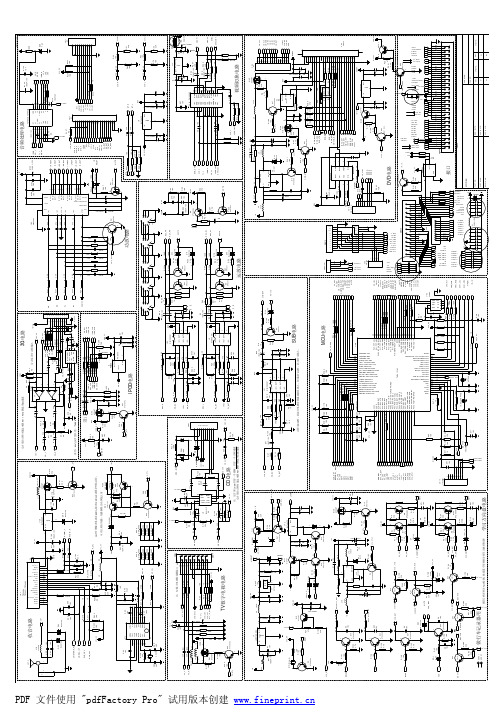
A5主板原理理图
收音电路
R27 NC
21 20
安吉星差分音频输入
E128 3300U/25V 10uF/16V
ANT GND GND ISS_STATUS FSU ADJCH AMST/MP SSTOP SDA SCL +5V MPXW AFS QUALY_OUT GND R_OUT L_OUT GND +8_5V
IN2 AUX-IN IN3 OUT2+ GND2 OUT25 2 3 8
3
RAR_TXD RAR_RXD 3G_DP 3G_DN
OUT
IN
1 R215 R216 R213 R214
225 0R 0R NC NC
R359
R170 NC CDC-L
1 2 3 4 5 6 7 8 0Y 2Y Y-COM 3Y 1Y INH VEE VSS VDD 2X 1X X-COM 0X 3X A B
Q46 KTC8050S
AUXLIN
2
C66 30P GPS-R R239 RCA_FR RCA_RR C18 104 R67 10K R240 47K 47K R166 1K
3 1 2 RMUTE 1 1 3
4.332M R238 R165 1K
VREV
C65 30P 3.3K B9V 100R 100R B9V E37 D12 R194 RLS4148 2.2K 10uF/16V 8 104 1 7
GND
注:TV/数字电视转接板接口
R141 3 5 VQ7
KTC8550S 3 2 RMUTE VREV CON4
CON14 47K 47K R148 3.3K D8 R193 RLS4148 2.2K +B12V 6 4 E69 100uF/16V C86 104 R68 10K R201 100K R18 R58 10K R300 RR_OUT R294 51K C136 101
ASR6501 ASR6502应用开发DEMO说明说明书
密级状态:绝密( ) 秘密() 内部资料(√) 公开()文档编号: (芯片型号) –ASR6501/ASR6502 (英文、数字)翱捷科技(上海)有限公司ASR Microelectronics Co., Ltd(版本所有,翻版必究)版本历史Table of Contents1概述 (5)2准备 (6)2.1 硬件准备 (6)2.2 软件安装 (7)2.3 SDK获取 (7)2.3.1 Git获取 (7)2.3.2 直接下载 (7)2.4 联网准备(联网通信需要) (8)2.4.1 节点信息申请 (8)2.4.2 网关配置 (8)3DEMO程序说明 (9)3.1 Demo简介 (9)3.2 ASR6502与ASR6501的区别 (9)3.3 代码结构 (10)3.4 代码流程 (11)3.5 LoRaWan配置与修改说明 (12)3.5.1 三元组修改 (12)3.5.2 入网方式修改 (12)3.5.3 ClassC修改 (13)3.5.4 频道掩码修改 (13)3.5.5 Mac参数修改 (13)3.6 外设使用说明 (13)3.6.6 GPIO (13)3.6.7 UART (18)3.6.8 I2C (21)3.6.9 SPI (23)3.6.10 Timer (25)3.6.11 外设组件文档说明 (25)4软件编译与烧录 (26)4.1 编译 (26)4.2 烧录 (27)4.2.1 PSoC Creator烧录 (27)4.2.2 PSoC Programmer烧录 (29)4.2.3 J-Flash烧录 (31)4.3 调试 (36)4.4 UART升级 (37)5低功耗 (39)5.1 配置低功耗 (39)5.2 低功耗唤醒 (39)5.3 新增外设低功耗处理 (39)6Q&A (41)6.1 如何修改SDK支持XO晶振? (41)6.2 如何在代码中更改设备信息? (41)6.3 如何使用ABP模式? (41)6.4 设备无法烧录? (41)6.5 SDK编译不通过? (42)7参考资料 (43)7.1 ALIOS资料 (43)7.2 LoRaWan资料 (43)7.3 PSOC4资料 (43)1 概述本文档主要对ASR6501/ASR6502 SDK中的lorawan demo程序进行说明,方便客户在ASR6501/ASR6502上进行应用程序的二次开发。
飞兆快捷(仙童)半导体选用指南 - FairChild
Video switch & filter
FMS6400 FMS6414 FSAV330 FSAV433 FMS6501 FMS6151 FMS6410 FSAV430 FSHDMI04AS/86AS FDS6982AS/84AS/86AS FDS6900AS FDS6900AS FDS8884/FDS8878 FDS8884/FDS8878 FDS6680AS/90AS FDS6680AS/90AS FDQ7238AS FDQ7238AS FDMS9600 FDMS9600 FDMS9620 FDMS9620
FAN5067 Dual switch FAN5068 DDR/ACPI FAN5077/78 DDR/ACPI iAMT FAN1582 FAN1655 2.5V RAMBUS 3.3V SDRAM 5V DUAL 3.3V DUAL
AGP
SMBus
North Bridge
uBGA
1.8V 2.5V SMBus
我们的承诺 一流的品质,一流服务,一流的价格.满足客户的要求! 所有出售产品均符合ROHS声明,达到环保要求,以保护环境为己任! 只销售全新原装现货,做有诚信的企业!
Flypowers
+86 755 8825 7825
企业文化
专业 分工 提供高效率服务的组织架构 在组织的规划上,飞捷首重专业与分工。配合各品牌的业务需求,我们采行独立运作团队的方式 落实效率管理,专业的产品经理,业务精英及应用工程师,我们坚持用最高绩效的要求,提供客 户最佳化的完美服务;为缩短客户产品上市时程,我们更成立了坚强的研发团队,以 Total Solution 的方式协同开发,共同创造产品的附加价值。「实时有效的服务」才是通路的真价值,为 了贯彻此一目标,我们不但广设据点仓库,就近服务客户,并成立高品质的信息及储运工作团 队,结合无形的信息服务以及实体的运筹作业上,让客户感受最佳化的服务。不但如此,针对策 略性客户的需求,飞捷更提供单一窗口,全员服务的效率运作,我们深信唯有不断的提升自我, 才能在剧烈多变的竞争中出。 品牌精耕 为各品牌产品设计最适切的经营策略,确实精耕。 异域专责 根据不同产品应用领域,提 供具有专门经验之销售团队为客户提供最专业的务 单一窗口针对策略性客户,由营运管理中心设 立专属部门,单 一窗口,全员服务。 精实后勤架构坚强信息及储运工作团队,提供一流运筹绩 效。 协同开发专业研发部门提供完整产品行销解决方案,缩短客户产品上市时程。 Flypowers +86 755 8825 7825
LM359
理工学院毕业设计外文资料翻译学院:理工学院专业:电子信息工程姓名:边治朋学号: 08L0701201外文出处:附件: 1.外文资料翻译译文;2.外文原文。
指导教师评语:签名:年月日附件1:外文资料翻译译文LM358使用手册1.电源范围3~30V2.低电源电流消耗与电源电压无关。
典型值为 0.7 mA 。
3. 共模输入电压范围宽度,包括接地。
低输入偏置与偏移参数:1.输入失调电压的典型值为3mV 。
2.输入失调电流的典型值为2nA 。
3.输入偏置电流的典型值为20nA 。
4.差分输入电压范围等于最大额定电压为±32V 。
5.开环差分电压放大的典型值为100 V/mV 。
内部频率补偿这个芯片包括两个独立的,高增益,频率补偿运算放大器。
适合于电源电压范围很宽的单电源使用,也是用于双电源工作模式。
两个电源之间的差值为3 V 至30 V ,和VCC 至少必须比共模输入电压高1.5 V。
LM358引脚图应用包括传感器放大器,直流放大器,和所有传统的运算放大器电路,现在可以更容易地在单电源电压系统实施。
例如,在数字系统中使用的标准5 V电源供电情况下可以直接操作这个芯片,电子接口无需额外的±5 V电源。
LM358的温度范围-25℃至125℃。
绝对最大额定值以上经营自由空气的温度范围内(除非另有说明)。
LM358 单位电源电压,VCC 32 V差分输入电压,VID±32 V输入电压VI–0.3 to 32 V接地输出短路持续时间(放大器)在(或低于)25°C自由空气的温度(Vcc≤15伏)(见注3)无限连续总功耗见耗散评价表经营自由的空气温度范围TA 0 to 70 °C存储温度范围,Tstg –65 to 150 °C外壳温度为60秒260 °C铅为60秒温度1,6毫米(1/16英寸)300 °C10秒的铅温度1,6毫米(1/16英寸)260 °C耗散评等表包装额定功率Ta≤25 °C降额因子TA= 25°CTA=70℃额定功率TA= 85°C额定功率TA= 125°C额定功率D 725 mW 5.8 mW/ °C 464 mW 377 mW 145 mWFK 1375 mW 11.0 mW/ °C 880 mW 715 mW 275 mW JG 1050 mW 8.4 mW/°C 672 mW 546 mW 210 mW P 1000 mW 8.0 mW/°C 640 mW 520 mW 200 mW PW 525 mW 4.2 mW/ °C 336 mW 273 mW在指定的自由空气温度的电气特性参数测试条件测试温度LM358单位最小典型值最大输入失调电压VCC= 5 V至最25℃ 3 7 mV大,全范围9平均温度系数输入失调电压全范围7 µV/ ℃输入失调电流VO=14V25℃ 2 50nA 全范围150平均气温系数输入失调电流全范围10 pA/°C输入偏置电流VO=14V25℃–20 –250nA 全范围-500共模输入电压范围VCC= 5 V至最大,25℃0至VCC-1.5V全范围0至VCC-2高电平输出电压RL≥ 2 k Ω25°C VCC–1.5V RL≥ 10 kΩ25°CVCC=最大RL=2kΩ全范围26RL≥10kΩ全范围27 28低电平输出电压RL ≤ 10 kΩ全范围 5 20 mV大信号差电压差放大VCC= 15 V,VO=1V至11V,RL= ≥ 2 kΩ25℃25 100V/mV全范围15共模抑制比VCC = 5 V 至最大,VIC=VICR(min)25°C 65 80 dB电源电压抑制比VCC = 5V到最大25°C 65 100 dB串音衰减f = 1 kHz to 20kHz25°C 120 dB输出电流VCC=15,VID=1 V,VO= 025°C –20 –30mA全范围–10VCC=15 V,VID=1 V,V o =15 V,25°C 10 20全范围 5VID = –1V,VO= 200 mV25°C 12 30 µA短路输出电流VCC=5 V,GND=-5V,VO= 025°C ±40 ±60 mA供电电流(两个放大器)VO= 2.5 V,无负载全范围0.7 1.2mA VCC= 最大,VO= 0.5 V,无负载全范围 1 2所有的特点是测量零共模输入电压开环的条件下,除非另有规定。
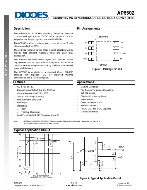
AP6502数据手册
Notes:
2. Stresses greater than the 'Absolute Maximum Ratings' specified above may cause permanent damage to the device. These are stress ratings only; functional operation of the device at these or any other conditions exceeding those indicated in this specification is not implied. Device reliability may be affected by exposure to absolute maximum rating conditions for extended periods of time.
Soft-Start Control Input. SS controls the soft-start period. Connect a capacitor from SS to GND to set the soft-start period. A 0.1µF capacitor sets the soft-start period to 15ms. To disable the soft-start feature, leave SS floating.
Pin Descriptions
Pin # 1
2
3 4 5
6 7 8 EP
Name BS
IN
SW GND FB
COMP EN SS EP
Description
High-Side Gate Drive Boost Input. BS supplies the drive for the high-side N-Channel MOSFET switch. Connect a 0.01µF or greater capacitor from SW to BS to power the high side switch.
DVD用到的基本型号IC
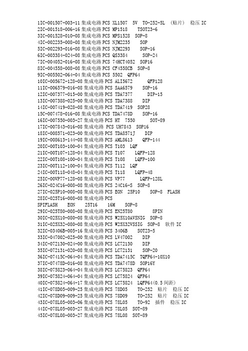
1IC-001507-003-11集成电路PCS XL1507 5V TO-252-5L (贴片) 稳压IC 2IC-001518-006-16集成电路PCS MP1518 TSOT23-63IC-001528-010-08集成电路PCS MPS1528 SOP-84IC-002235-008-08集成电路PCS NJM2235 SOP5IC-002293-016-08集成电路PCS NJM2293 SOP-166IC-003384-024-08集成电路PCS QS3384 SOP-247IC-004052-016-08集成电路PCS 74HCT4052 SOP168IC-004558-008-08集成电路PCS CF4558CB SOP-89IC-005502-064-04集成电路PCS 5502 QFP6410IC-005672-128-08集成电路PCS ALI5672 QFP12811IC-006579-016-08集成电路PCS SAA6579 SOP-1612IC-007377-015-00集成电路PCS TDA7377 DIP-1513IC-007388-025-00集成电路PCS TDA7388 DIP14IC-007419-028-08集成电路PCS TDA7419 SOP2815C-007478-016-08集成电路PCS TDA7478D SOP-1616IC-007550-003-27集成电路PCS HT 7550 SOT-8917IC-007843-016-08集成电路 PCS UH7843 SOP1618IC-008571-023-00集成电路PCS TDA8571J DIP19IC-008613-144-08集成电路PCS AML8613 QFP-14420IC-00T103-100-04集成电路PCS T103 LQF21IC-00T107-128-04集成电路PCS T107 LQFP-12822IC-00T108-100-04集成电路PCS T108 LQFP-10023IC-00T112-100-04集成电路PCS T112 LQF24IC-00T118-048-04集成电路PCS T118 LQFP-4825IC-00VP77-128-08集成电路PCS VP77 LQFP-128L26IC-024C16-008-08集成电路PCS 24C16-S SOP-827IC-025P10-008-08集成电路PCS EON 25P10 SOP-8 FLASH28IC-025T16-008-08集成电路PCS SPIFLASH EON 25T16 16M SOP-8 29IC-025T80-008-08集成电路PCS EN25T80 8PIN30IC-025X10-080-08集成电路PCS W25X10AVSNIG SOP-831IC-025X32-080-08集成电路PCS W25X32VSSIG SOP-8 软件IC32IC-03406B-005-16集成电路PCS 3406B SOT23-533IC-047002-025-00集成电路PCS LV47002 DIP34IC-072130-024-00集成电路PCS LC72130 DIP35IC-072131-020-08集成电路PCS LC72131 SOP-2036IC-07415C-064-04集成电路PCS TDA7415C TQFP64-10X1037IC-07478D-016-08集成电路PCS TDA7478D SOP16Y38IC-075823-064-04集成电路PCS LC75823 QFP6439IC-075824-064-04集成电路PCS LC75824 QFP6440IC-075824-064-17集成电路PCS LC75824 LQFP64(0.5间距)41IC-078D05-009-25集成电路PCS 78D05 TO-252 贴片稳压IC42IC-078D09-009-25集成电路PCS 78D09 TO-252 贴片稳压IC43IC-078L05-003-06集成电路PCS 78L05 TO-92 插件稳压IC44IC-078L05-003-27集成电路PCS 78L05 SOT-8945IC-078L08-003-27集成电路PCS 78L08 SOT-8946IC-078L09-003-27集成电路PCS 78L09 SOT-8947IC-078L12-003-27集成电路PCS 78L12 SOT-8948IC-078L18-003-06集成电路PCS 78L18 TO-92 插件稳压IC49IC-078L18-003-27集成电路PCS 78L18 SOT-8950IC-078M05-003-07集成电路PCS 78M05 TO-220 插件稳压IC51IC-078M05-005-25集成电路PCS 78M05 TO-252 贴片稳压IC52IC-078M08-005-25集成电路PCS 78M08 TO-252 贴片稳压IC53IC-078M09-005-25集成电路PCS 78M09 TO-252 贴片稳压IC54IC-08104L-128-17集成电路PCS SPHE8104L QFP12855IC-08202T-128-08集成电路PCS SPHE8202T-128PIN56IC-09259A-028-08集成电路PCS SA9259A HSOP-2857IC-0D7292-008-00集成电路PCS D7292 DIP-858IC-0L7805-003-07集成电路PCS L7805 TO-220 稳压IC59IC-0L7808-003-10集成电路PCS L7808 D2PAK(TO-263)60IC-0L7809-003-07集成电路PCS L7809 TO-220 稳压IC61IC-0LM393-008-08集成电路PCS LM393 SOP-862IC-0T100A-100-04集成电路PCS T100A QFP-10063IC-0T101A-100-04集成电路PCS T101A QFP-10064IC-3202DJ-006-16集成电路PCS MP3202DJ SOT23-665IC-3414AM-008-08集成电路PCS NJM3414AM SOP-866IC-36966U-208-04集成电路PCS ZR36966U MQFP208B-V967IC-74HC00-014-08集成电路PCS 74HC00 SOP1468IC-8202TQ-128-08集成电路PCS SPHE8202TQ QFP12869IC-AM1117-018-23集成电路PCS AMS1117-1.8V SOT-223 稳压IC70IC-AM1117-025-23集成电路PCS AMS1117-2.5V SOT-223 稳压IC71IC-AM1117-033-23集成电路PCS AMS1117-3.3V SOT-223 稳压IC72IC-AM1117-ADJ-23集成电路PCS AMS1117-ADJ SOT-223 稳压IC73IC-AM5888-028-08集成电路PCS AM5888 HSOP-2874IC-AP1507-005-03集成电路PCS AP1507-D05 TO-252 5V 稳压IC (贴片) 75IC-AP1507-ADJ-03集成电路PCS AP1507-ADJ TO-252 可调稳压IC (贴片) 76IC-AT1780-008-08集成电路PCS AT1780 SOP-877IC-AU6331-028-08集成电路PCS AU6331 SOP-2878IC-AX3008-048-04集成电路PCS AX3008 QFP4879IC-AX3800-048-04集成电路PCS AX3800 QFP4880IC-AX6901-003-16集成电路PCS AX6901 SOT-2381IC-BA3121-008-08集成电路PCS BA3121 SOP-882IC-BA5954-028-08集成电路PCS BA5954 HSOP2883IC-BA6247-010-00集成电路PCS BA6247 DIP-1084IC-BA6247-025-08集成电路PCS BA6247 HSOP-2585IC-BA6287-008-08集成电路PCS BA6287F SOP-886IC-BA6849-028-08集成电路PCS BA6849 HSOP2887IC-BA7071-008-08集成电路PCS BA7071 SOP888IC-BA7603-016-08集成电路PCS BA7603F SOP1689IC-BD3801-032-08集成电路PCS BD3801 SOP-3290IC-BU1924-016-08集成电路PCS BU1924 SOP-1691IC-BU4052-016-08集成电路PCS BU4052 SOP-1692IC-CD4066-014-08集成电路PCS CD4066 SOP-1493IC-CS4340-016-08集成电路PCS CS4340 SOP1694IC-CS4344-010-08集成电路PCS CS4344 TSSOP1095IC-CT4052-016-08集成电路PCS 74HCT4052 TSSOP1696IC-D0504F-006-21集成电路PCS UMD0504F SC70-6L97IC-D5668S-028-08集成电路PCS D5668S HSOP-28 驱动IC98IC-DS3501-010-08集成电路PCS DS3501 USOP-1099IC-EF4069-014-08集成电路PCS HEF4069 SOP14100IC-EF6621-032-08集成电路PCS TEF6621 SOP-32101IC-EF6624-032-08集成电路PCS TEF6624 SOP-32102IC-EGA32L-044-04集成电路PCS ATMEGA32L QFP-44 软件IC103IC-EONF80-008-08集成电路PCS FLASH EON F80-75HCP SOP-8 (FLASH) 104IC-ET6601-032-08集成电路PCS FET6601T SOP-32105IC-ET7201-006-16集成电路PCS ET7201T SOT23-6106IC-GM3157-003-23集成电路PCS SGM3157 SC70-6107IC-HC4094-016-08集成电路PCS 74HC4094 SOP-16108IC-HC4538-016-08集成电路PCS 74HC4538 TSSOP16109IC-HT1621-048-08集成电路PCS HT1621B SSOP-48110IC-HY1262-054-08集成电路PCS HY57V1262GTR-60C 128M TSOP-54111IC-HY1616-050-08集成电路PCS HY57V16160FTP-7 1M*16 TSOP50 HYNIX 112IC-HY6416-054-08集成电路PCS 64Mbit:HY57V641620HG T0SS-54113IC-I5A100-016-08集成电路PCS PI5A100 SOP-16114IC-IA7032-003-27集成电路PCS KIA7032 SOT-89115IC-JM2244-008-08集成电路PCS NJM2244 SOP-8116IC-JM2267-008-08集成电路PCS NJM2267 SOP8117IC-K4S641-054-08集成电路PCS SDRAM K4S641632K-UC609(1Mx16x4) 118IC-LA2733-003-16集成电路PCS LA2733 SOT23-5 X型119IC-LA3161-000-00集成电路PCS LA3161120IC-LB1641-010-00集成电路PCS LB1641 DIP-10121IC-MAX809-003-16集成电路PCS MAX809TEUR SOT-23122IC-MDSR05-004-03集成电路PCS UMDSR05 SOT143123IC-MP1410-008-08集成电路PCS MPS1410 SOP-8124IC-MP1540-005-16集成电路PCS MP1540 SOT23-5125IC-MP3202-008-24集成电路PCS MP3202DG QFN8126IC-MP4461-010-08集成电路PCS MP4461 QFN127IC-MS6501-028-08集成电路PCS FMS6501 SSOP28128IC-MS6502-024-08集成电路PCS FMS6502 TSSOP24129IC-N24C02-008-08集成电路PCS AN24C02 SOP-8 记忆IC130IC-PM9435-008-08集成电路PCS APM9435 SOP-8131IC-PT2222-024-08集成电路PCS PT2222-001 SOP24132IC-PT2312-032-08集成电路PCS PT2312 SOP133IC-PT2313-028-08集成电路PCS PT2313L SOP-28134IC-PT6523-064-04集成电路PCS PT6523 QFP-64135IC-RF7205-008-08集成电路PCS IRF7205 SOP8136IC-RF7309-008-08集成电路PCS IRF7309 SOP-8137IC-RT9164-003-23集成电路PCS RT9164-3.3V SOT-223138IC-SC2003-016-08集成电路PCS TSC2003 SOP-16139IC-SC2046-016-08集成电路PCS TSC2046 SSOP16140IC-SC7313-028-08集成电路PCS SC7313 SOP-28141IC-SI4702-020-08集成电路PCS SI4702 免调高频头IC(单FM) BGA20142IC-SI4703-020-08集成电路PCS SI4703 免调高频头IC(单FM/RDS) BGA20 143IC-SI4730-020-08集成电路PCS SI4730 免调高频头IC(AM/FM) BGA20144IC-SI4731-020-08集成电路PCS SI4731 免调高频头IC(AM/FM/RDS) BGA20 145IC-SL8499-016-08集成电路PCS ISL8499 TSSOP16146IC-SST39V-048-08集成电路PCS SST39VF1601 TSOP48147IC-ST720C-100-04集成电路PCS MST720C TQFP-100148IC-T1346A-008-08集成电路PCS AAT1346A SOP-8149IC-TA7291-009-00集成电路PCS TA7291S DIP150IC-TG7533-033-27集成电路PCS TG7533 3V3 SOT-89151IC-TL4094-008-08集成电路PCS TL4094B SOP-8152IC-TW8816-128-04集成电路PCS TW8816-DALB3-GR QFP-128153IC-TW8826-128-04集成电路PCS TW8826 QFP-128154IC-W25X10-008-08集成电路PCS W25X10VSNIG SOP8155IC-XC6202-003-27集成电路PCS XC6202P502PR S0T-89。
6502UE安全与声音产品说明书

Belden believes this product to be in compliance with all applicable environmental programs as listed in the data sheet. The information provided is correct to the best of Belden's knowledge, information and belief at the date of its publication. This information is designed only as a general guide for the safe handling, storage, and any other operation of the product itself or the one that it becomes a part of. The Product Disclosure is not to be considered a warranty or quality specification. Regulatory information is for guidance purposes only. Product users are responsible for determining the applicability of legislation and regulations based on their individual usage of the product.
- 1、下载文档前请自行甄别文档内容的完整性,平台不提供额外的编辑、内容补充、找答案等附加服务。
- 2、"仅部分预览"的文档,不可在线预览部分如存在完整性等问题,可反馈申请退款(可完整预览的文档不适用该条件!)。
- 3、如文档侵犯您的权益,请联系客服反馈,我们会尽快为您处理(人工客服工作时间:9:00-18:30)。
Description
The FMS6502 provides eight inputs that can be routed to any of six outputs. Each input can be routed to one or more outputs, but only one input may be routed to any output. Each input supports an integrated clamp option to set the output sync tip level of video with sync to ~300mV. Alternatively, the input may be internally biased to center output signals without sync (Chroma, Pb, Pr) at ~1.25V. All outputs are designed to drive a 150Ω DC-coupled load. Each output can be programmed to provide either 0dB or 6dB of signal gain. Input-to-output routing and input bias mode functions are controlled via an I2C-compatible digital interface.
Packing Method
Rail Reel
© 2006 Fairchild Semiconductor Corporation Rev. 1.0.0
元器件交易网
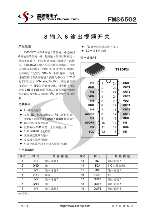
FMS6502 8-Input, 6-Output Video Switch Matrix with Output Drivers, Input Clamp, and Bias Circuitry
Switching ■ I2CTM-Compatible Digital Interface, Standard Mode ■ 3.3V or 5V Single Supply Operation ■ Pb-Free TSSOP-24 Package
Applications
■ Cable and Satellite Set-Top Boxes ■ TV and HDTV Sets ■ A / V Switchers ■ Personal Video Recorders (PVR) ■ Security and Surveillance ■ Video Distribution ■ Automotive (In-Cabin Entertainment)
Description
Input, channel 1 Must be tied to ground Input, channel 2 Positive power supply Input, channel 3 Must be tied to ground Input, channel 4 Selects I2C address Input, channel 5 Selects I2C address Input, channel 6 Serial clock for I2C port Input, channel 7 Serial data for I2C port Input, channel 8 Must be tied to ground Output, channel 6 Output, channel 5 Output, channel 4 Positive power supply Output, channel 3 Output, channel 2 Output, channel 1 Must be tied to ground
Pb-Free
Yes Yes
Operating Temperature Range
-40°C to 85°C -40°C to 85°C
Package
24-Lead Thin Shrink Small Ouline Package 24-Lead Thin Shrink Small Ouline Package
© 2006 Fairchild Semiconductor Corporation FMS6502 Rev. 1.0.0
2
元器件交易网
FMS6502 8-Input, 6-Output Video Switch Matrix with Output Drivers, Input Clamp, and Bias Circuitry
The I2C-compatibe interface is used to program output enables, input-to-output routing, and input bias configuration. The I2C address of the FMS6502 is 0x06 (0000 0110) with the ability to offset based upon the values of the ADDR0 and ADDR1 inputs. Offset addresses are defined below:
Parameter
Min.
Typ.
Max.
150 150 300
Unit
°C °C °C °C/W
Recommended Operating Conditions
The Recommended Operating Conditions table defines the conditions for actual device operation. Recommended operating conditions are specified to ensure optimal performance to the datasheet specifications. Fairchild does not recommend exceeding them or designing to Absolute CC Supply Voltage Range
Parameter
Operating Temperature Range
Min.
-40 3.135
Typ.
5.0
Max.
85 5.25
Unit
°C V
Electrostatic Discharge Information
Symbol
HBM CDM
FAIRCHILD
3
FMS6502
4 21
4 5 6 7 8 9 10 11 12 13 14 15 16 17 18 19 20 21 22 23 24
24L TSSOP
5 6 7 8 9 10 11 12 20 19 18 17 16 15 14 13
Figure 2. Pin Configuration
Parameter
Human Body Model (JEDEC: JESD22-A114) Charged Device Model (JEDEC: JESD22-A101)
Value
10 2
Unit
kV kV
© 2006 Fairchild Semiconductor Corporation FMS6502 Rev. 1.0.0
Absolute Maximum Ratings
Stresses exceeding the absolute maximum ratings may damage the device. The device may not function or be operable above the recommended operating conditions and stressing the parts to these levels is not recommended. In addition, extended exposure to stresses above the recommended operating conditions may affect device reliability. The absolute maximum ratings are stress ratings only.
3
元器件交易网
FMS6502 8-Input, 6-Output Video Switch Matrix with Output Drivers, Input Clamp, and Bias Circuitry
Digital Interface
Pin Configuration
Pin Description
Pin#
1 2 3
22
IN1 GND IN2 VDD IN3 GND IN4 ADDR1 IN5 ADDR0 IN6 SCL
1 2
24 23
GND OUT1 OUT2 OUT3 VDD OUT4 OUT5 OUT6 GND IN8 SDA IN7
Features
■ 8 x 6 Crosspoint Switch Matrix ■ Supports SD, PS, and HD 1080i / 1080p Video ■ Input Clamp and Bias Circuitry ■ Doubly Terminated 75Ω Cable Drivers ■ Programmable 0dB or 6dB Gain ■ AC- or DC-Coupled Inputs ■ AC- or DC-Coupled Outputs ■ One-to-One or One-to-Many Input-to-Output
元器件交易网