最新EPSON晶振汇总
epson晶体晶振
epson晶体晶振Epson晶体晶振是一种用于电子设备中稳定提供时钟信号的元件。
晶体振荡器是一种能够产生稳定频率的振荡器,它利用晶体的谐振特性来实现。
Epson晶体晶振在电子设备中扮演着非常重要的角色。
它的主要作用是提供稳定的时钟信号,以确保设备的正常运行。
在许多电子设备中,如计算机、手机、电视等,都需要一个准确的时钟信号来同步各个部件的操作,以便实现正确的功能。
Epson晶体晶振的工作原理是利用晶体的谐振特性。
晶体是一种具有晶格结构的固体材料,当施加电场或机械力时,晶体会发生微小的形变,从而产生电荷的位移。
这种位移会导致晶体的谐振频率发生变化,进而产生稳定的振荡信号。
Epson晶体晶振的制造过程非常精细复杂。
首先,需要选取高纯度的晶体材料,如石英晶体,然后通过特定的工艺将晶体加工成具有特定结构和尺寸的晶片。
接下来,将晶片与电极进行连接,形成晶体振荡器。
最后,通过测试和筛选,选择出频率稳定性好、工作可靠的晶体振荡器。
Epson晶体晶振具有许多优点。
首先,它具有非常高的频率稳定性和精确度,能够提供准确的时钟信号。
其次,它具有低功耗和小尺寸的特点,非常适合集成在各种电子设备中。
此外,Epson晶体晶振还具有抗干扰能力强、工作温度范围广等优势。
在实际应用中,Epson晶体晶振通常以表面贴装的形式存在。
这种封装方式可以使晶振元件更加紧凑,方便安装和布局。
同时,Epson晶体晶振还可以根据不同的应用需求提供不同的频率和精度选择,以满足各种设计要求。
Epson晶体晶振是一种非常重要的电子元件,它在各种电子设备中扮演着提供稳定时钟信号的关键角色。
通过利用晶体的谐振特性,Epson晶体晶振能够产生高精度、高稳定性的振荡信号,为设备的正常运行提供保障。
随着科技的不断发展,Epson晶体晶振的性能和应用领域也在不断拓展,将为电子设备的发展带来更多可能性。
爱普生osc有源晶振 SG-9101CB晶体振荡器 规格书资料

►Designed for automotive applications such as Car Multimedia, Body Electronics, Remote Keyless Entry etc.
►Designed for automotive applications related to driving safety (Engine Control Unit, Air Bag, ESC etc ).
NOTICE:PLEASE READ CAREFULLY BELOW BEFORE THE USE OF THIS DOCUMENT ©Seiko Epson Corporation 2020 ――――――――――――――――――――――――――――――――――――――――――――――――――――
1. The content of this document is subject to change without notice. Before purchasing or using Epson products, please contact with sales representative of Seiko Epson Corporation (“Epson”) for the latest information and be always sure to check the latest information published on Epson’s official web sites and resources.
All of our major manufacturing and non-manufacturing sites, in Japan and overseas, completed the acquisition of ISO 14001
爱普生 EPSON 温补晶振 TG-5006CE-39L 32.000000MHz规格参数、数据手册、规格书信息

*2 Measured in the elapse of 24 hours after reflow soldering.
*3 Vcc +/- 5% must be in operating supply voltage range (1.7 V to 3.465 V)
2
[ 5 ] Electrical characteristics
3
[ 6 ] Test circuit
1) Output Load : Load_R // Load_C = 10 kΩ // 10 pF
Supply Voltage
By-pass Capacitor
0.01 to 0.1 F
Vcc N.C.
OUT
DC-cut Capacitor
GND
Load_C
fo
-
32
-
MHz
Frequency tolerance
f_tol
-1.0
-
+1.0
x10⁻⁶
T_use=+25°C+/-2°C Before reflow
Frequency tolerance *1
f_tol
-2.0
-
+2.0
x10⁻⁶
T_use=+25°C+/-2°C After 2 reflows *2
To maintain stable operation, provide a 0.01 to 0.1 μF by-pass capacitor at a location as near as possible to the power source terminal of the crystal product (between Vcc - GND).
爱普生晶振SG-3030CM晶体振荡器规格书

-40 °C ~ +85 °C +5±23 × 10-6
+10 × 10-6 / -120 × 10-6 ±2 × 10⁻⁶ / V Max.
2 µA Max.
45 % ~ 55 %
输出电压
VOH VOL
输出负载条件(CMOS) L_CMOS
VIO -0.4V Min. 0.4V Max. 15 pF Max.
未对任何专利或知识版权的许可权进行授权。 ·本材料中规格表中的数值大小通过数值线上的大小关系表示。 ·当出口此材料中描述的产品或技术时,你应该遵守相应的出口管制法律和法规,并按照这些法律和法规的要求执行。
请不要将产品(以及任何情况下提供任何的技术信息)用于开发或制造大规模杀伤性武器或其他军事用途。还要求,不要将产品提供给任何 将产品用于此类违禁用途的第三方。 ·此类产品是基于在一般电子机械内使用而设计开发的,如将产品应用于需要极高可靠性的特定用途,必须实现得到弊公司的事前许可。若 无许可弊公司将不负任何责任。
1.太空设备(人造卫星、火箭等) 2.运输车辆机器控制装置(汽车、飞机、火车、船舶等) 3.用于维持生命的医疗器械 4.海底中转设备 5.发电站控制机器 6.防灾防盗装置 7.交通设备 8.其他,用于与 1~7 具有同等可靠性的用途。
本材料中记载的品牌名称或产品名称是其所有人的商标或注册商标。
Seiko Epson Corporation
CD RF
CG
V IO OUT
GND
条件
裸存 +25 °C, VCC=3.3V -20 °C ~ +70 °C (+25 C 为基准温度) +25 °C, 3.3V, 无负载条件 1/2VCC(VIO) 级别 IOH=-0.4mA IOL= 0.4mA CMOS 负载 CMOS 负载:20 % VCC(VIO) ~ 80 % VCC(VIO) 级别 电源电压最低时,所需时间为 0 秒. +25 °C +25 °C,VCC=3.3 V, 第一年
爱普生晶振MC-146 32.768kHz 7pF (Q13MC1462000100)
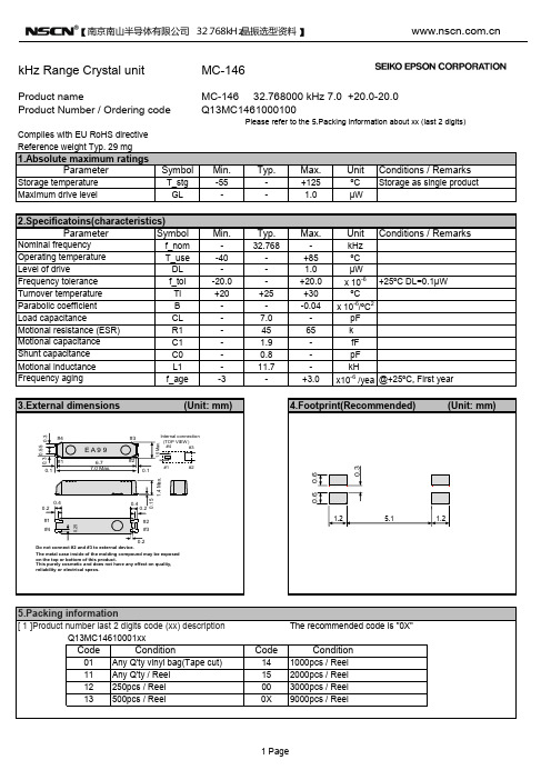
Unit: mm
2 Page
(4.8)
【 南京南山半导体有限公司 32.768kHz晶振选型资料 】
Reflow profile
Pre Heating Temperature Tp1 ~ Tp2 = + 170 °C Heating Temperature TMlt = + 220 °C Peek Temperature TMax. = + 260 °C Point of measuring In case of Solder ability Terminal. In case of Resistance to soldering heat Surface.
Nominal frequency Operating temperature Level of drive Frequency tolerance Turnover temperature Parabolic coefficient Load capacitance Motional resistance (ESR) Motional capacitance Shunt capacitance Motional inductance Frequency aging f_nom T_use DL f_tol Ti B CL R1 C1 C0 L1 f_age
Temperature
+260ºC
TMax.
+220ºC
Tmlt
Tp2
Tp1
35s
100s
t(time)
Notice
· This material is subject to change without notice. · Any part of this material may not be reproduced or duplicated in any form or any means without the written permission of Seiko Epson. · The information about applied data,circuitry, software, usage, etc. written in this material is intended for reference only. Seiko Epson does not assume any liability for the occurrence of customer damage or infringing on any patent or copyright of a third party. This material does not authorize the licensing for any patent or intellectual copyrights. · When exporting the products or technology described in this material, you should comply with the applicable export control laws and regulations and follow the procedures required by such laws and regulations. · You are requested not to use the products (and any technical information furnished, if any) for the development and/or manufacture of weapon of mass destruction or for other military purposes. You are also requested that you would not make the products available to any third party who may use the products for such prohibited purposes. · These products are intended for general use in electronic equipment. When using them in specific applications that require extremely high reliability, such as the applications stated below, you must obtain permission from Seiko Epson in advance. / Space equipment (artificial satellites, rockets, etc.) / Transportation vehicles and related (automobiles, aircraft, trains, vessels, etc.) / Medical instruments to sustain life / Submarine transmitters / Power stations and related / Fire work equipment and security equipment / Traffic control equipment / And others requiring equivalent reliability. · All brands or product names mentioned herein are trademarks and/or registered trademarks of their respective.
epson晶振选型手册
Epson晶振选型手册引言概述:Epson晶振选型手册是一本提供关于Epson晶振选型的专业指导手册。
晶振作为一种重要的电子钟振装置,广泛应用于各类电子设备中,对于设备的稳定性和精准性起到关键作用。
本手册将从多个方面介绍Epson晶振的选型原则和方法,以帮助读者准确选型和应用。
正文内容:1. 晶振的基本原理1.1 晶振的作用与功能1.1.1 提供时钟信号1.1.2 稳定电子设备的工作频率1.1.3 控制和同步各设备之间的通信1.1.4 精确计时和定时功能1.2 晶振的工作原理1.2.1 晶体振荡原理1.2.2 纯谐振条件与频率稳定性1.2.3 晶振的构造与材料选择2. Epson晶振的特点与优势2.1 高稳定性和低功耗2.1.1 稳定性与频率偏移2.1.2 低功耗对电池寿命的影响2.2 宽温度范围和长寿命2.2.1 温度对晶振频率的影响2.2.2 长期使用的可靠性和稳定性2.3 大容量和小封装尺寸2.3.1 容量对数据传输速率的影响2.3.2 封装尺寸对电路板设计的要求3. Epson晶振选型原则3.1 需求分析和参数确定3.1.1 设备类型和用途3.1.2 工作频率和精度要求3.1.3 温度范围和环境影响3.2 选择适合的晶振类型3.2.1 晶振频率范围和精度等级3.2.2 温度补偿和温度响应特性3.2.3 封装尺寸和安装要求3.3 参考设计和测试验证3.3.1 参考电路设计3.3.2 振荡电路测试和频率测量3.3.3 选型结果评估和优化4. Epson晶振选型案例分析4.1 移动方式晶振选型4.1.1 高稳定性和小封装尺寸的需求4.1.2 多频段应用的选择考虑4.2 电子表计晶振选型4.2.1 长期使用和温度范围要求4.2.2 低功耗和电池寿命的平衡4.3 工业自动化控制晶振选型4.3.1 高频率和精度要求4.3.2 多通道同步和控制4.3.3 长寿命和可靠性的考虑5. Epson晶振应用注意事项5.1 环境温度和封装要求5.2 抗振动和抗干扰性能5.3 防静电措施和电源干扰5.4 长期使用和老化问题结语:本手册全面介绍了Epson晶振的选型原则和方法,包括晶振的基本原理、Epson晶振的特点与优势、选型原则、案例分析以及应用注意事项。
EPSON晶振

MC-146晶振
MC-146是日本爱普生株式会社(EPSON)生产的小尺寸贴片32.768kHz时钟晶振。
爱普生株式会社是日本精工-爱普生集团下属子公司,专注于石英晶振、IC等电子元器件和打印耗材、办公用品等生产厂家。
在行业内颇具知名度。
MC-146晶振广泛应用于手机、PHS、PDA、数码相机、GPS模块、FM调谐模块、Zigbee、血糖值测量仪、信用卡结算机、各种微机的预备时钟、无绳电话、移动设备等。
其基本规格如下:
标称频率:32.768kHz
频率偏差:+/-20ppm
负载电容:6PF、7PF、12.5PF
工作温度:-40-+85°C
等效电阻:65KΩmax
MC-146晶振产品特征:
厚度最大为1.4mm的薄型产品
适用于高密度按照及自动化安装SMD型产品
内置了高信赖性、经过光刻加工的圆柱型石英晶振
优良的耐冲击性、耐热性
符合ROHS标准。
MC-146晶振外形尺寸:
长度:7.00mmmax 宽度:1.50mmmax厚度:1.40mm max
上海唐辉电子是日本爱普生株式会社(EPSON)在中国的指定代理商,唐辉电子在PPTC自恢复保险丝、PTC热敏电阻、晶体谐振器、振荡器系列、高品质电容、电感和液晶屏产品、IC 类等领域有很强的竞争力。
产品广泛应用在通信、电脑、消费类电子及网络产品、仪器仪表、工控系统、安防产品、电源供应器等产品上积极面对市场及客户的多方位要求,坚持以最好的品牌和最具竞争力的价格销售电子零件,为客户提供多元化的服务,务求充分满足客户的要求,致力于成为中国乃至世界最佳元器件供应商之一。
epson 爱普生晶振SG-310系列贴片有源晶振规格书

裸存 -20 C ~ +70 C -40 C ~ +85 C -20 C ~ +70 C -30 C ~ +85 C -40 C ~ +85 C 无负载条件, 2 MHz f0 4 MHz 无负载条件, 4 MHz<f0 8 MHz 无负载条件, 8 MHz<f016 MHz 无负载条件, 16 MHz<f025 MHz 无负载条件, 25 MHz<f033 MHz 无负载条件, 33 MHz<f048 MHz 无负载条件, 48 MHz<f080 MHz
实际尺寸
规格(特征)
项目 输出频率范围 电源电压 储存温度 工作温度 符号 f0 VCC T_stg T_use SG-310 SEF SG-310 SDF SG-310 SCF SG-310 SDN SG-310 SCN 2.000 MHz ~ 48.000 MHz 3.000 MHz ~ 80.000 MHz 1.8 V Typ. 2.5 V Typ. 3.3 V Typ. 2.5 V Typ. 3.3 V Typ. 1.6 V ~ 2.2 V 2.2 V ~ 3.0 V 2.7 V ~ 3.6 V 2.2 V ~ 2.7 V 2.7 V ~ 3.6 V -40 C ~ +125 °C -40 C ~ +85 °C B: 50 10-6, C: 100 10-6 L: 50 × 10-6, M: 100 10-6 – D:±20 × 10-6 ,S:±25 × 10-6 – R:±25 × 10-6 ,P:±20 × 10-6 – J:±25 × 10-6 1.5 mA Max. 1.5 mA Max. 1.5 mA Max. 1.5 mA Max. 1.5 mA Max. 2.0 mA Max. 1.5 mA Max. 2.0 mA Max. 2.5 mA Max. 4.0 mA Max. 5.0 mA Max. 2.0 mA Max. 2.0 mA Max. 2.5 mA Max. 2.0 mA Max. 2.5 mA Max. 3.5 mA Max. 3.0 mA Max. 3.5 mA Max. 4.5 mA Max. – 6.0 mA Max. 7.0 mA Max. 0.7 A Max. 1.5 A Max. 2.0 A Max. 10 µA Max. (0.2 A Typ.) (0.5 A Typ.) (1.0 A Typ.) 45 % ~ 55 % 45 % ~ 55 % 45 % ~ 55 % 45 % ~ 55 % 40 % ~ 60 % 40 % ~ 60 % 90 % VCC Min. 10 % VCC Max. 15 pF Max. 80 % VCC Min. 70 % VCC Min. 20 % VCC Max. 30 % VCC Max. 4 ns Max. 10 ms Max. 2 ms Max. 5 10-6 / year Max. 3 10-6 / year Max. – 10 10-6 Max. 条件
爱普生 EPSON 差分晶振 SG7050VAN 100.000000MHz规格参数、数据手册、规格书信息
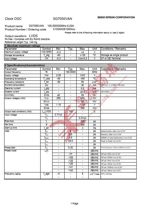
Clock OSC SG7050VANProduct name SG7050VAN 100.000000MHz KJGAProduct Number / Ordering code X1G0042810004xxPlease refer to the 9.Packing information about xx (last 2 digits) Output waveform LVDSPb free / Complies with EU RoHS directiveReference weight Typ. 149 mg1.Absolute maximum ratingsParameter Symbol Min.Typ.Max.Unit Conditions / Remarks Maximum supply voltage Vcc-GND-0.3-+4V-Storage temperature T_stg-40-+125ºC Storage as single product Input voltage Vin-0.3-Vcc+0.3V ST or OE Terminal2.Specifications(characteristics)Parameter Symbol Min.Typ.Max.Unit Conditions / Remarks Output frequency f0-100.0000-MHzSupply voltage Vcc 2.25- 3.63V-Operating temperature T_use-40-+85ºC-Frequency tolerance f_tol-50-50x10-6-Current consumption Icc--30mA OE=Vcc L_LVDS=100 ohmStand-by current I_std--0.0mA-Disable current I_dis--20.0mA OE=GNDSymmetry SYM45-55%-Output voltage(LVDS)V OD250-450mV-dV OD--50mV-Vos 1.15- 1.35V-dVos--150mV-Output load condition(LVDS)L_LVDS-100-Ω-Input voltage V IH0.7Vcc---V IL--0.3Vcc-Rise time t r--300ps-Fall time tf--300ps-Start-up time t_str--3ms-Jitter t DJ-8-ps Deterministic Jitter Vcc=2.5VT RJ- 2.6-ps Random Jitter Vcc=2.5Vt RMS- 4.6-psδ(RMS of total distribution) Vcc=2.5Vt p-p-28.5-ps Peak to Peak Vcc=2.5Vt acc---ps-Phase jitter t PJ-0.32-ps Off set Frequency: 12kHz to 20MHz Vcc=2.5V Phase noise L(f)---dBc/Hz---77-dBc/Hz Off set 10Hz Vcc=2.5V--109-dBc/Hz Off set 100Hz Vcc=2.5V--125-dBc/Hz Off set 1kHz Vcc=2.5V--135-dBc/Hz Off set 10kHz Vcc=2.5V--141-dBc/Hz Off set 100kHz Vcc=2.5V--142-dBc/Hz Off set 1MHz Vcc=2.5V Frequency aging f_age-5-5x10⁻⁶/Year25℃,1stYear----3.Test circuit1) To observe waveform and current (case 1)* To measure the disable current, OE pin is connected to GND2) To observe waveform and current (case 2)* The lines from OUT and OUT pin are same length.3) Measurement condition A) Oscilloscope•Bandwidth should be 5 times higher than DUT’s output frequency (4 GHz).•Probe ground should be placed closely from test point and lead length should be as short as possible.B) By-pass capacitor 1 (approx. 0.01 μF to 0.1 μF) places closely between Vcc and GND.C) By-pass capacitor 2 (approx. 10 μF) places closely between power supply terminals on the board.D) Use the current meter whose internal impedance value is small.E) Power supply• Start up time (0 Vg90 %Vcc) of power source should be more than 150 μs and slew rate should be less than 19.8 mV/μs.• Impedance of power supply should be as low as possible.Vcc+3.3 VOE NC OUTGNDDifferentila probe AOUT100 ΩOscillo- scopeBy-pass capacitor 2 Power supply 1OE pin*By-pass capacitor 1Vcc+3.3 VOE NCOUTGNDOUT50 Ω50 ΩV OSV ODVV By-pass capacitor 2 Power supply 1OE pinBy-pass capacitor 1A4.Timing chart5.External dimensions (Unit: mm)6.Footprint(Recommended) (Unit: mm)To maintain stable operation, provide a 0.01uF to 0.1uF by-pass capacitor at a location as near as possible to the power source terminal of the crystal product (between Vcc - GND).Each output waveform (OUT, and OUT)GNDtwtOUTSYM = tw / tOUTV OS1V OS2dV OS =|V OS1-V OS2|50 % of OUT amplitude50 % of OUT amplitudeVccDifferential output waveform (OUT – OUT)tftr Differential 0 V 80 % of amplitude 20 % of amplitudeOUTV OD2V OD1dV OD =|V OD1-V OD2|OUT#5 #4#6 #2 1.805.084.202.00#1 #31.807.Reflow profileReflow condition (Follow of JEDEC STD-020D.01)8.Example of schematic layoutTemperature [ ︒C ] 60 300 250200 150 100 50ts60 s to 180 s( +150 ︒C to +200 ︒C )Avg. Ramp-up 3 ︒C / s Max.Ramp-down 6 ︒C / s Max.Time [ s ]120 180 240 300 360 420 480 540 600 660 720 780Ts min ; +150 ︒CTs max ; +200 ︒C TL; +217 ︒C+255 ︒CtL60 s to 150 s( +217 ︒C over )tp ; 20 s to 40 sTP ; +260 ︒C Time +25 ︒C to PeakThis figure shows an example of this product’s application schematic.As with any high speed analog circuitry, the power supply pins for this device are vulnerable to noise. In order to achieve optimum jitter performance, power isolation with filter device is required for power supply pins.In order to achieve best performance of the power isolation filter, it is recommended that the filter composing devices is placed on the device side of the PCB as close to the power pins as possible. The component value of this filter is just an example, it may have to be adjusted.9.Packing information[ 1 ]Product number last 2 digits code(xx) descriptionThe recommended code is "00"X1G0042810004xxCode Code 01Any Q'ty vinyl bag(Tape cut)13500pcs / Reel 11Any Q'ty / Reel 001000pcs / Reel12250pcs / ReelConditionCondition * By-pass capacitor (approx. 0.01 μF to 0.1 μF) places closely between Vcc and GND.* By-pass capacitor (approx. 10 μF) places closely between power supply terminals on the board. * Please design the two output lines by characteristic impedance 100 Ω and same length, and try to make the output lines as short as possible.[ 2 ] Taping specificationSubject to EIA-481 & IEC-60286(1) Tape dimensions Material of the Carrier Tape : PS Material of the Top Tape : PET+PEUnit: mmSymbol A B C D E F Value φ1.5489.2516 2.3(2) Reel dimensionsCenter material : PS Material of the Reel : PSA BDECFTop tapeCarrier tape10.Notice∙This material is subject to change without notice.∙Any part of this material may not be reproduced or duplicated in any form or any means without the written permissionof Seiko Epson.∙The information about applied circuitry, software, usage, etc. written in this material is intended for reference only.Seiko Epson does not assume any liability for the occurrence of infringing on any patent or copyright of a third party.This material does not authorize the licensing for any patent or intellectual copyrights.∙When exporting the products or technology described in this material, you should comply with the applicableexport control laws and regulations and follow the procedures required by such laws and regulations.∙You are requested not to use the products (and any technical information furnished, if any) for the developmentand/or manufacture of weapon of mass destruction or for other military purposes. You are also requested that youwould not make the products available to any third party who may use the products for such prohibited purposes.∙These products are intended for general use in electronic equipment. When using them in specific applications that require extremely high reliability, such as the applications stated below, you must obtain permission from Seiko Epson in advance. / Space equipment (artificial satellites, rockets, etc.)/ Transportation vehicles and related (automobiles, aircraft, trains, vessels, etc.)/ Medical instruments to sustain life/ Submarine transmitters/ Power stations and related/ Fire work equipment and security equipment/ Traffic control equipment/ And others requiring equivalent reliability.∙All brands or product names mentioned herein are trademarks and/or registered trademarks of their respective.。
爱普生晶振型号大全
爱普生晶振型号大全本文由/doc/c510992735.html,整理合成爱普生公司成立于1942年5月,总部位于日本长野县诹访市,是数码映像领域的全球领先企业。
爱普生集团通过富有创新和创造力的文化,提升企业价值,致力于为客户提供数码影像创新技术和解决方案。
爱普生拓优科梦是一家专业从事晶体元件的厂商,爱普生拓优科梦的晶体元器件已以23%的市场占有率位于业界第一。
在2010年晶振全球厂家排名中,占据首位。
爱普生仅此一项水晶振动子行业就能足矣让电子世界的人都敬佩不已。
爱普生晶振以32.768KHZ晶振称霸晶振行业,主要消费在手机,PCB,等电子产品。
同时爱普生以提供原子钟的精准振荡器知名业界。
仅此在音叉振子和振荡器还远远达不到爱普生本身的要求。
他们要求的是在元器件占领NO1。
因此除了KHZ,MHZ的研究发展,另外还发明GHZ 技术,使工艺技术达到人无完人,史前无例,实现以基波方式产生2.5GHz为止高频的表面声波(SAW)元器件。
爱普生拓优科梦把半导体(IC)称之为“产业之米”,并认为晶体元器件更是离不开的“产业之盐”。
将进一步致力于小型、高稳定、高精度晶体元器件的开发,为现有的应用程序以及生活新蓝图开拓广阔前景。
爱普生晶振在KHZ,MHZ,以及GHZ上都有重大突破,使得爱普生拓优科梦的晶体元器件已以23%的市场占有率位于业界第一。
那我们说说爱普生KHZ的产品工艺吧,爱普生KHZ产品分有圆柱DIP和贴片SMD。
KHZ中爱普生是以32.768KHZ最为出名的。
32.768K晶振是一款数字电路板都要使用到的重要部件,有人比喻为电路板的心跳发生器,也就是说心如果停止了跳动,那么电路板也将无法进行稳定的工作了。
32.768K中爱普生C-002RX是一款受欢迎的圆柱音叉晶振,体积只有2*6mm。
与精工的VT-200-F,西铁城的CFS206,KDS的DT-26同体积同参数。
因此说道的四款型号晶振都是可以相互替换使用的。
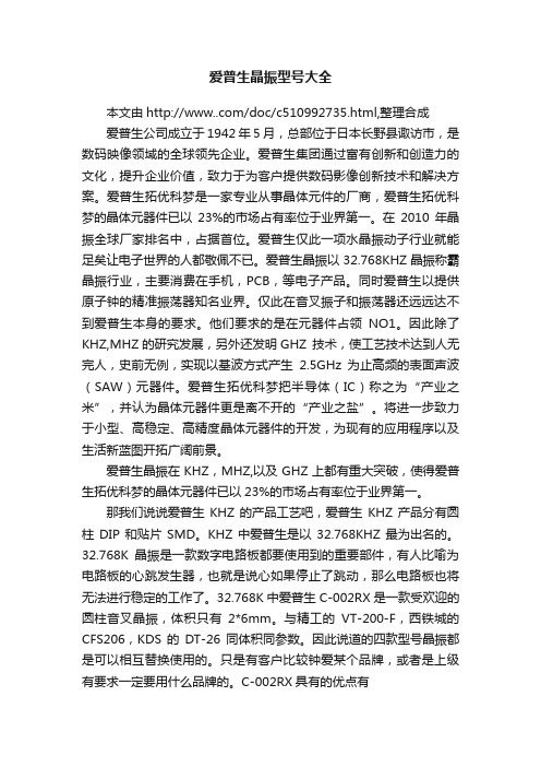
爱普生 EPSON 无源贴片晶振 TSX-3225 24.000000MHz规格参数、数据手册、规格书信息
f_nom
Frequency tolerance
f_tol
Frequency Stability over temperature
f_tem
Operating temperature
T_use
Level of drive
DL
Load capacitance
CL
Motional resistance (ESR)
R1
Motional capacitance
C1
Motional inductance
L1
Shunt capacitance
C0
Frequency aging
f_age
Min.
- -10
-20
-40 10 - -1
Typ.
24.000000 -
-
100 9
3.48 12.64 1.27 -
Max.
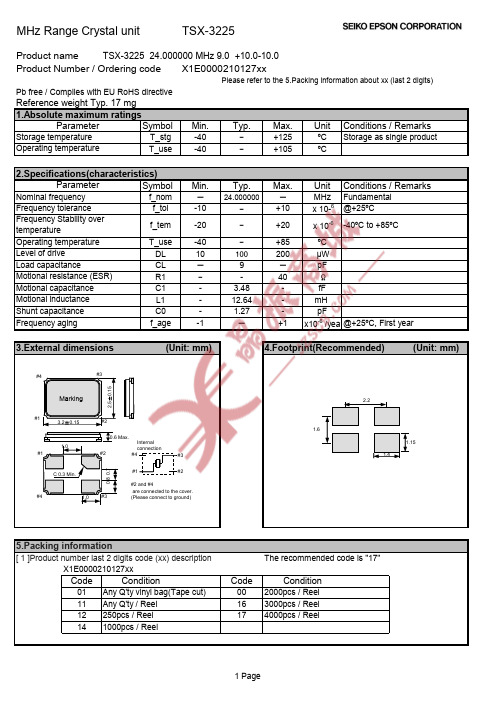
TG5032CBN EPSON 5032高稳定度温补晶振TCXO选型资料
fo-Tc
× 10-6
-0.25
-
+0.25
T_use=-40°C to +85°C (Option Spec.)
-0.1
-
+0.1 Load+/-10% (~40MHz)
-0.2
-
+0.2 Load+/-10% (~50MHz)
Frequency / load coefficient
fo-Load × 10-6
Clipped sine wave output
DC-cut capacitor *1 Clipped sine wave output
*1 DC-cut capacitor is not included in this TCXO. Please attach an external DC-cut capacitor (0.01 μF Min.) to the out pin.
►Designed for automotive applications such as Car Multimedia, Body Electronics, Remote Keyless Entry etc.
►Designed for automotive applications related to driving safety (Engine Control Unit, Air Bag, ESC etc ).
【EPSON晶振官网认证中国代理商 —南京南山半导体有限公司】
Ultra high stability temperature compensated crystal oscillator Product name : TG5032CBN / TG5032SBN
爱普生晶振SG-8002CE可编程晶体振荡器规格书
30 mA Max.
-
25 mA Max.
16 mA Max. 16 mA Max.
OE=GND (PT.PH,PC) ( SG-8002LB) OE=GND (PH,PC) ( SG-8002LB)
I_std
50 µA Max.
ST =GND (ST,SH,SC)
40 % ~ 60 %
-
TTL load: 1.4 V ,
CMOS *1 L_CMOS
-
15 pF Max.
(SG-8002LB)
15 pF Max.
25 pF Max
15 pF Max. (SG-8002CA / JA / DC / DB)
VIH VIL
2.0 V Min. 0.8 V Max.
70 % VCC Min. 20 % VCC Max.
OE
ST
1.4 -0.15
5.08
1.6
2.54
1.8 C (ex. 0.01 µF)
Resist 5.08
SG-8002JC
10. 5 Max.
#4
#3
SOJ 4pin 10.5x5.8x2.7 mm
Package and pin compatible with SG-636.
1.3
5. 0 5.8 Max.
#1 13.7 Max. #4
7. 62
SG-8002DB
DIP full size
#14
#8
6. 36
16.0000 C 2PH EPSON 9357B
#1 19.8 Max. #7 7.62
0.51
0.2M in .
7. 62
90 °~ 105 °
常用25MHZ晶振型号封装大全
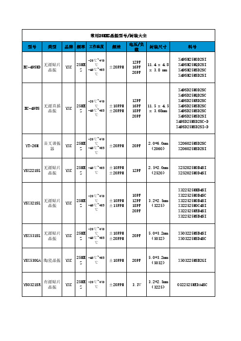
-40℃~+85 ℃
±25PPM ±50PPM
3.3V
3.2*2.5mm (3225)
Q33310N70002711 Q33310N70008911
SG310SCN
有源贴片 晶振
EPSON
25MH Z
-40℃~+85 ℃
±50PPM
2.7~3.6V
3.2*2.5mm (3225)
Q33310F70032100
O503225MEDC6MI O705025MEDB6MI
TSX-3225
无源贴片 晶振
EPSON
25MH Z
-40℃~+85 ℃
±10PPM
9PF 10PF 12PF 16PF 18PF 20PF
3.2*2.5mm (3225)
X1E000021062112 X1E000021013300 X1E000021013312 X1E000021013900 X1E000021064800 X1E000021014012 X1E000021064812 X1E000021035200
-20℃~+70
无源贴片 YSX531SL 晶振
YXC
25MH ℃ Z -40℃~+85
±10PPM ±20PPM
℃
20PF
5.0*3.2mm (5032)
X503225MSB4SI X503225MSD4SC
YSX530GA 陶瓷晶振
YXC
25MH -40℃~+85
Z
℃
±10PPM
20PF
5.0*3.2mm (5032)
OP252025MADA4SI-u OP252025MEDA4SI-u OP322525MEDA4SI-u OP503225MEDA4SI-u OP705025MADA4SI-u OP705025MEDA4SI-u
爱普生 EPSON 有源贴片晶振 SG-3030CM 32.768000kHz规格参数、数据手册、规格书信息
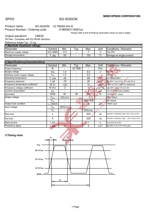
SPXO SG-3030CMProduct nameSG-3030CM 32.768000 kHz B Product Number / Ordering code X1B0002110001xxPlease refer to the 8.Packing information about xx (last 2 digits)Output waveform CMOSPb free / Complies with EU RoHS directiveReference weight Typ. 13 mg1.Absolute maximum ratings ParameterSymbolMin.Typ.Max.UnitConditions / RemarksMaximum supply voltage Vcc-GND -0.3-7V Vcc PinStorage temperatureT_stg-55-125ºCStorage as single product2.Specifications(characteristics)ParameterSymbolMin.Typ.Max.UnitConditions / RemarksOutput frequencyf0-32.7680-kHz Supply voltageVcc 1.5- 5.5V Vcc Pin Interface power supply voltage V IO 1.5- 5.5VIO PinOperating temperatureT_use -40-85ºC No condensationFrequency tolerancef_tol -18-28x10-6@+25℃, Vcc=3.3V , 5+/-23x10^-6Frequency temperature coefficient f0-Tc -120-10x10-6-20℃ to 70℃ (+25℃ is reference)Frequency voltage coefficient f0-Vcc -2-2x10⁻⁶ /V `@+25℃ Vcc=1.5V to 5.5V Current consumption Icc --2μA Vcc=3.3V No load condition Symmetry SYM 455055%1/2Vcc(VIO )Level Output voltage V OH VIO-0.4--IOH=-400μA V OL --GND+0.4IOL=400μAOutput load condition L_CMOS --15pFCMOS Load Input voltage V IH 80%Vcc---V IL--20%Vcc -Rise time t r --200ns Fall time tf --200ns Start-up time t_str --1sVcc=2.0V to 5.0VFrequency agingf_age-5-5x10⁻⁶@+25℃ Vcc=3.3V First year3.Timing chart20%VIO ⇔ 80%VIO 15pF VIO=1.5V to 5.5V 20%VIO ⇔ 80%VIO 15pF VIO=1.8V to 5.5VGNDV CC tr 50 %V CCttw80 %V CC20 %V CC tf4.Test circuit1) Waveform observation 2) Current consumption*Current consumption under the disable function should be = GND.3) Condition (1) Oscilloscope· Band width should be minimum 5 times higher (wider) than measurement frequency.· Probe earth should be placed closely from test point and lead length should be as short as possible.* Recommendable to use miniature socket. (Don’t use earth lead.)(2) L_CMOS also includes probe capacitance.(3) By-pass capacitor (0.01 mF to 0.1 mF) is placed closely between VCC and GND.(4) Use the current meter whose internal impedance value is small.(5) Power supply· Start up time (0 %VCC ® 90 %VCC) of power source should be more than 150 ms.· Impedance of power supply should be as lowest as possible.V CCSTOUTGNDswichsupplyby-pass capacitorTest PointAor OEor OEV CCSTOUTGNDsupplyby-passcapacitorL_CMOSTest Point5.External dimensions (Unit: mm)6.Footprint(Recommended) (Unit: mm)7.Reflow profileReflow condition (Follow of JEDEC STD-020D.01)8.Packing information[ 1 ]Product number last 2 digits code(xx) descriptionThe recommended code is "00"X1B0002110001xxCode Code 01Any Q'ty vinyl bag(Tape cut)141000pcs / Reel 11Any Q'ty / Reel 152000pcs / Reel 12250pcs / Reel003000pcs / ReelConditionConditionTemperature [ ︒C ] 60 300 250200 150 100 50ts60 s to 180 s( +150 ︒C to +200 ︒C )Avg. Ramp-up 3 ︒C / s Max.Ramp-down 6 ︒C / s Max.Time [ s ]120 180 240 300 360 420 480 540 600 660 720 780Ts min ; +150 ︒CTs max ; +200 ︒C TL; +217 ︒C+255 ︒CtL60 s to 150 s( +217 ︒C over )tp ; 20 s to 40 sTP ; +260 ︒C Time +25 ︒C to Peak3.2±0.22.351.5±0.2#2 #1 #2#4#30.9 M a x .#30.65 0.5#1#40.4Pin mapPin Connection 1 V IO 2 GND 3 OUT 4 V CC3030 ○B123B1.052.651.20.8[ 2 ] Taping specificationSubject to EIA-481 & IEC-60286(1) Tape dimensions Material of the Carrier Tape : PS Material of the Top Tape : PET+PEUnit: mm(2) Reel dimensionsCenter material : PS Material of the Reel : PSφ1.0 ±0.1+0.14.0±0.12.0±0.054.0±0.110P: 40±0.15.5±0.05+0.312.0-0.11.75±0.13.6±0.10.3±0.051.0±0.11.9±0.1TopG 穴Φ76 mmΦ160 mmH Φ3Φ180 mm +015.40±1 mm13.00±0.3 mmΦ60 mmΦ21±0.8 mmΦ13±0.2 mm2.00 mm +0.39.Notice·This material is subject to change without notice.·Any part of this material may not be reproduced or duplicated in any form or any means without the written permission of Seiko Epson.·The information about applied data,circuitry, software, usage, etc. written in this material is intended for reference only.Seiko Epson does not assume any liability for the occurrence of customer damage or infringing on any patent or copyright of a third party.This material does not authorize the licensing for any patent or intellectual copyrights.·When exporting the products or technology described in this material, you should comply with the applicable export control laws and regulations and follow the procedures required by such laws and regulations.·You are requested not to use the products (and any technical information furnished, if any) for the development and/or manufacture of weapon of mass destruction or for other military purposes. You are also requested that youwould not make the products available to any third party who may use the products for such prohibitedpurposes.·These products are intended for general use in electronic equipment. When using them in specific applications that requireextremely high reliability, such as the applications stated below, you must obtain permission from Seiko Epson in advance./ Space equipment (artificial satellites, rockets, etc.)/ Transportation vehicles and related (automobiles, aircraft, trains, vessels, etc.)/ Medical instruments to sustain life/ Submarine transmitters/ Power stations and related/ Fire work equipment and security equipment/ Traffic control equipment/ And others requiring equivalent reliability.。
进口晶振料号、尺寸大全
本电波工业株式
晶体谐振器
频率
NX2520SG
19.2-54MHZ
NX3215SA
32.768KHZ
NX2520SA
16-80MHZ
NX3225SA
12-150MHZ
NX3225GA
9.840-50MHZ
NX5032GB
12-55MHZ
NX5032GA
8-55MHZ
NX5032SD
9.75-40MHZ
AV
9.9 ~ 54MHz
8Z
12 ~ 54MHz
石英振荡器
7W
1 ~ 170MHz
7C
1 ~ 150MHz
7X
1 ~ 125MHz
8W
4 ~ 54MHz
VCXO 压控振荡器
BK
60 ~ 700MHz
CJ
60 ~ 200MHz
TCXO 温补振荡器
7Q
13 ~ 52MHz
7L
13 ~ 52MHz
NDK(日
瑞士微晶
音叉晶振
精工晶振
KHZ谐振器
NX2012SA NX3215SA
日本NDK晶振
KHZ谐振器 M晶体谐振器 NhomakorabeaNX3215SA NX1612AA NX1612AA NX2016SA NX2520SA NX3225GA NX5032GA NX5032SA NX1255GB NR-2B NR-2C AT-41CD2
1.5~80
KV7050B-C3
1.5~170
石英晶体振荡器(TCXO)
KT2520 KT3225
13~52 13~52
2.5 x 2.0 x 0.7 3.2 x 2.5 x 0.89 5.0 x 3.2 x 1.2 5.0 x 3.2 x 1.0 5.0 x 3.2 x 1.1 7.0 x 5.0 x 1.6
(整理)EPSON晶振.

EPSON 晶振一,EPSON简介;Epson Toyocom即爱普生拓优科梦,运用长年积累的培育人工石英以及以加工为代表的、实现精微化、高精度、高品质的3D战略”。
究极应用石英特性而制造的三大元器件而成的模块,成为不可缺少的企业而迈进至今。
伴随信息化社会的进程,现在石英元器件已被广泛应用于各种电子设备以及家电产品之中日趋重要。
爱普生拓优科梦Epson Toyocom,将进一步究极用精微加工发挥“石英”材料的优越性能的“QMEMS”技术小、更高性能或全新功能的元器件,同时融合爱普生集团的半导体与软件技术增添便于使用、能让顾客更体验到利用价值的“解决方案”。
通过上述工作,我们将为社会的的发展以及实现更舒畅的未来而竭诚奉献。
二,EPSON 制造工厂及销售渠道;EPSON在日本本土有三个制造工场关联制造工场。
在海外拥有中国苏州、无锡、马来西亚和泰国四个制造工场。
EPSON拥有遍布全球的销售网络,全球共分为四极少数的代理商。
日本KDS上海唐辉电子人员均来自日本KDS大真空。
如原深圳KDS营业主任罗成刚现为上海唐辉电子高级经理,原上海KDS原营业部主任周宇现为上海唐辉电子销售总监,原天津KDS郭建中为上海唐辉电子深圳公司经理,原苏州KDS胡鸣现为上海唐辉电子苏州办经理.三,EPSON 产品分类;EPSON产品种类齐全,主要产品如下;1、SMD Crystal Resonators/MHz Band Crystal Resonators2、SMD Tuning Fork Crystal Resonators/KHz Band Crystal Resonators3,Miniature Crystal Resonators/MHz Band Crystal Resonators4、Crystal Resonators/MHz Band Crystal Resonators5、Tuning Fork Crystal Resonators/KHz Band Crystal Resonators6、SPXO7、VCXO8、TCXO9、VC-TCXO 10、SSXO 11、Filters四,EPSON晶振的工作原理;石英晶体振荡器是利用石英晶体(二氧化硅的结晶体)的压电效应制成的一种谐振器件,它的基本结构大致是从一块石英晶体上按一定方位角切下薄片(简称为晶片,它可以是正方形、矩形或圆形等),在它的两个对应面上涂敷银层作为电极,在每个电极上各焊一根引线接到管脚上,再加上封装外壳就构成了石英晶体谐振器,简称为石英晶体或晶体、晶振。
爱普生晶振MC-30A系列32.768K晶振规格书
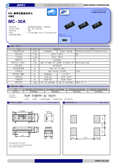
实际尺寸规格(特征)kHz 频率范围晶体单元车载用 MC - 30A∙频率范围: 32.768 kHz (20 kHz ~ 120 kHz)∙外部尺寸规格 : 8.0 × 3.8 × 2.54 mm ∙谐波次数: 基频∙应用: 汽车音响,ECU 子时钟,汽车导航系统,时钟∙依据AEC-Q200产品号码(请联系我们) Q1xMC30A2xxxx00推进环境管理体系 符合国际标准在环境管理体系的运行方面,使用ISO14001国际环境标准,通过“计划-实施-检查-验证(PDCA)的循环来实现持续改进。
公司位于日本和海外的主要制造基地已取得了ISO14001资格认证。
追求高品质Seiko Epson 为了向顾客提供高品质、卓越信赖性的产品、服务,迅速着手通过ISO 9000系列资格认证的工作,其日本和海外工厂也在通过ISO 9001认证。
同时,也在通过大型汽车制造厂商要求规格的ISO/TS 16949认证。
关于在目录内使用的记号●无铅。
●符合欧盟RoHS 指令。
欧盟RoHS 指令免检的含铅产品。
(密封玻璃、高温熔化性焊料或其他材料中包含铅。
)●为汽车方面的应用,如汽车多媒体、车身电子、遥控无钥门锁等。
●为汽车行驶安全方面的应用(引擎控制单元、气囊、电子稳定程序控制系统)。
注意事项·本材料如有变更,恕不另行通知。
量产设计时请确认最新信息。
·未经Seiko Epson 公司书面授权,禁止以任何形式或任何方式复制或者发布本材料中任何部分的信息内容。
·本材料中的书面信息、应用电路、编程、使用等内容仅供参考。
Seiko Epson 公司对第三方专利或版权的侵权行为不负有任何责任。
本材料未对任何专利或知识版权的许可权进行授权。
·本材料中规格表中的数值大小通过数值线上的大小关系表示。
·当出口此材料中描述的产品或技术时,你应该遵守相应的出口管制法律和法规,并按照这些法律和法规的要求执行。
- 1、下载文档前请自行甄别文档内容的完整性,平台不提供额外的编辑、内容补充、找答案等附加服务。
- 2、"仅部分预览"的文档,不可在线预览部分如存在完整性等问题,可反馈申请退款(可完整预览的文档不适用该条件!)。
- 3、如文档侵犯您的权益,请联系客服反馈,我们会尽快为您处理(人工客服工作时间:9:00-18:30)。
E P S O N晶振
EPSON 晶振
一,EPSON简介;
Epson Toyocom即爱普生拓优科梦,运用长年积累的培育人工石英以及以加工为代表的、实现精微化、高精度、高品质的综合技术提出“3D战略”。
究极应用石英特性而制造的三大元器件定时元器件、传感元器件、光学元器件,并创出将其复合而成的模块,成为不可缺少的企业而迈进至今。
伴随信息化社会的进程,现在石英元器件已被广泛应用于各种电子设备以及家电产品之中日趋重要。
爱普生拓优科梦Epson Toyocom,将进一步究极用精微加工发挥“石英”材料的优越性能的“QMEMS”技术创造出更小、更高性能或全新功能的元器件,同时融合爱普生集团的半导体与软件技术增添便于使用、能让顾客更体验到利用价值的“解决方案”。
通过上述工作,我们将为社会的的发展以及实现更舒畅的未来而竭诚奉献。
二, EPSON 制造工厂及销售渠道;
EPSON在日本本土有三个制造工场,有四个和精工的关联制造工场。
在海外拥有中国苏州、无锡、马来西亚和泰
国四个制造工场。
EPSON拥有遍布全球的销售网络,全球共分为四个大区,即美国、欧洲、亚洲、澳洲四区。
另外在大陆地区有极少数的代理商。
日本KDS上海唐辉电子人员均来自日本KDS大真空。
如原深圳KDS营业主任罗成刚现为上海唐辉电子高级经理,原上海KDS原营业部主任周宇现为上海唐辉电子销售总监,原天津KDS郭建中为上海唐辉电子深圳公司经理,原苏州KDS胡鸣现为上海唐辉电子苏州办经理.
三, EPSON 产品分类;
EPSON产品种类齐全,主要产品如下;
1、SMD Crystal Resonators/MHz Band Crystal Resonators
2、SMD Tuning Fork Crystal Resonators/KHz Band Crystal
Resonators
3,Miniature Crystal Resonators/MHz Band Crystal Resonators
4、Crystal Resonators/MHz Band Crystal Resonators
5、Tuning Fork Crystal Resonators/KHz Band Crystal Resonators
6、SPXO
7、VCXO
8、TCXO
9、VC-TCXO 10、SSXO 11、Filters
四, EPSON晶振的工作原理;
石英晶体振荡器是利用石英晶体(二氧化硅的结晶体)的压电效应制成的一种谐振器件,它的基本结构大致是从一块石英晶体上按一定方位角切下薄片(简称为晶片,它可以是正方形、矩形或圆形等),在它的两个对应面上涂敷银层作为电极,在每个电极上各焊一根引线接到管脚上,再加上封装外壳就构成了石英晶体谐振器,简称为石英晶体或晶体、晶振。
其产品一般用金属外壳封装,也有用玻璃壳、陶瓷或塑料封装的。
石英晶体的压电效应:若在石英晶体的两个电极上加一电场,晶片就会产生机械变形。
反之,若在晶片的两侧施加机械压力,则在晶片相应的方向上将产生电场,这种物理现象称为压电效应。
注意,这种效应是可逆的。
如果在晶片的两极上加交变电压,晶片就会产生机械振动,同时晶片的机械振动又会产生交变电场。
在一般情况下,晶片机械振动的振幅和交变电场的振幅非常微小,但当外加交变电压的频率为某一特定值时,振幅明显加大,比其他频率下的振幅大得多,这种现象称
为压电谐振,它与LC回路的谐振现象十分相似。
它的谐振频率与晶片的切割方式、几何形状、尺寸等有关。
五,EPSON晶振的制程;
六,EPSON晶振的内部结构;
七,全球主要晶振厂商排名
八,EPSON晶振入库包装
,
九,EPSON晶振的主要参数;
1、标称频率F:晶体元件规范(或合同)指定的频率。
HZ赫兹 KHZ、MHZ
2、调整频差:在规定条件下,基准温度(常温25°C)时工作频率相对标称频率的允许偏离。
(PPM)
3、温度频差:在整个工作温度范围内,相对于基准温度时,工作频率的允许偏离。
4、负载电容CL:与晶体元件一起决定负载谐振频率的外置有效外界电容。
5、工作温度:晶体能稳定工作的温度范围。
6、工作电压:指有源晶振工作时的供电电压。
7、总频差:由于指定或多种原因引起的工作频率相对于标称频率的最大允许偏差。
主要由调整频差和温度频差构成。
8、基准温度:一般指±25℃±2℃,对温控晶体元件是指控温范围的中点。
十, EPSON晶振的应用领域;
EPSON产品在业界属于高端产品,其应用偏向中高端市场。
产品广泛应用于电表、水表等计量仪表、汽车电子、工业控制系统、金融微电子、医疗电子设备、高端消费类产品、通信终端和网络设备、便携式产品等行业。
十一,EPSON晶振未来的发展趋势;
石英晶体元件小型化是电子产品更新换代的要求。
随着技术的进步与科学的发展,电子产品不断地更新换代:数码相机、摄像机不断取代传统的光学相机、摄像机,DVD取代VCD,平板电视逐渐取代显像管电视,笔记本电脑越来越多地取代台式电脑,集GPS、蓝牙、相机、MP3于一身
精品资料
的多功能3G手机将取代2G手机,所有这些电子产品的换代几乎都需要体积更小、性能更好的石英晶体元件为之配套。
EPSON,爱普生电子产品的便携式、数字化、节能、低功耗已成为社会发展的趋势。
仅供学习与交流,如有侵权请联系网站删除谢谢11。