DSP滤波器中英文对照外文翻译文献
图像处理中值滤波器中英文对照外文翻译文献
中英文资料对照外文翻译一、英文原文A NEW CONTENT BASED MEDIAN FILTERABSTRACTIn this paper the hardware implementation of a contentbased median filter suitabl e for real-time impulse noise suppression is presented. The function of the proposed ci rcuitry is adaptive; it detects the existence of impulse noise in an image neighborhood and applies the median filter operator only when necessary. In this way, the blurring o f the imagein process is avoided and the integrity of edge and detail information is pre served. The proposed digital hardware structure is capable of processing gray-scale im ages of 8-bit resolution and is fully pipelined, whereas parallel processing is used to m inimize computational time. The architecturepresented was implemented in FPGA an d it can be used in industrial imaging applications, where fast processing is of the utm ost importance. The typical system clock frequency is 55 MHz.1. INTRODUCTIONTwo applications of great importance in the area of image processing are noise filtering and image enhancement [1].These tasks are an essential part of any image pro cessor,whether the final image is utilized for visual interpretation or for automatic an alysis. The aim of noise filtering is to eliminate noise and its effects on the original im age, while corrupting the image as little as possible. To this end, nonlinear techniques (like the median and, in general, order statistics filters) have been found to provide mo re satisfactory results in comparison to linear methods. Impulse noise exists in many p ractical applications and can be generated by various sources, including a number of man made phenomena, such as unprotected switches, industrial machines and car ign ition systems. Images are often corrupted by impulse noise due to a noisy sensor or ch annel transmission errors. The most common method used for impulse noise suppressi on n forgray-scale and color images is the median filter (MF) [2].The basic drawback o f the application of the MF is the blurringof the image in process. In the general case,t he filter is applied uniformly across an image, modifying pixels that arenot contamina ted by noise. In this way, the effective elimination of impulse noise is often at the exp ense of an overalldegradation of the image and blurred or distorted features[3].In this paper an intelligent hardware structure of a content based median filter (CBMF) suita ble for impulse noise suppression is presented. The function of the proposed circuit is to detect the existence of noise in the image window and apply the corresponding MFonly when necessary. The noise detection procedure is based on the content of the im age and computes the differences between the central pixel and thesurrounding pixels of a neighborhood. The main advantage of this adaptive approach is that image blurrin g is avoided and the integrity of edge and detail information are preserved[4,5]. The pro posed digital hardware structure is capable of processing gray-scale images of 8-bitres olution and performs both positive and negative impulse noise removal. The architectt ure chosen is based on a sequence of four basic functional pipelined stages, and parall el processing is used within each stage. A moving window of a 3×3 and 5×5-pixel im age neighborhood can be selected. However, the system can be easily expanded to acc ommodate windows of larger sizes. The proposed structure was implemented using fi eld programmable gate arrays (FPGA). The digital circuit was designed, compiled and successfully simulated using the MAX+PLUS II Programmable Logic Development S ystem by Altera Corporation. The EPF10K200SFC484-1 FPGA device of the FLEX1 0KE device family was utilized for the realization of the system. The typical clock fre quency is 55 MHz and the system can be used for real-time imaging applications whe re fast processing is required [6]. As an example,the time required to perform filtering of a gray-scale image of 260×244 pixels is approximately 10.6 msec.2. ADAPTIVE FILTERING PROCEDUREThe output of a median filter at a point x of an image f depends on the values of t he image points in the neighborhood of x. This neighborhood is determined by a wind ow W that is located at point x of f including n points x1, x2, …, xn of f, with n=2k+1. The proposed adaptive content based median filter can be utilized for impulse noisesu p pression in gray-scale images. A block diagram of the adaptive filtering procedure is depicted in Fig. 1. The noise detection procedure for both positive and negative noise is as follows:(i) We consider a neighborhood window W that is located at point x of the image f. Th e differences between the central pixel at point x and the pixel values of the n-1surr ounding points of the neighborhood (excluding thevalue of the central pixel) are co mputed.(ii) The sum of the absolute values of these differences is computed, denoted as fabs(x ). This value provides ameasure of closeness between the central pixel and its su rrounding pixels.(iii) The value fabs(x) is compared to fthreshold(x), which is anappropriately selected positive integer threshold value and can be modified. The central pixel is conside red to be noise when the value fabs(x) is greater than thethreshold value fthresho d(x).(iv) When the central pixel is considered to be noise it is substituted by the median val ue of the image neighborhood,denoted as fk+1, which is the normal operationof the median filter. In the opposite case, the value of the central pixel is not altered and the procedure is repeated for the next neighborhood window.From the noised etection scheme described, it should be mentioned that the noise detection level procedure can be controlled and a range of pixel values (and not only the fixedvalues of 0 and 255, salt and pepper noise) is considered asimpulse noise.In Fig. 2 the results of the application of the median filter and the CBMF in the gray-sca le image “Peppers” are depicted.More specifically, in Fig. 2(a) the original,uncor rupted image“Peppers” is depicted. In Fig. 2(b) the original imagedegraded by 5% both positive and negative impulse noise isillustrated. In Figs 2(c) and 2(d) the resultant images of the application of median filter and CBMF for a 3×3-pixel win dow are shown, respectively. Finally, the resultant images of the application of m edian filter and CBMF for a 5×5-pixelwindow are presented in Figs 2(e) and 2(f). It can be noticed that the application of the CBMF preserves much better edges a nddetails of the images, in comparison to the median filter.A number of different objective measures can be utilized forthe evaluation of these results. The most wi dely used measures are the Mean Square Error (MSE) and the Normalized Mean Square Error (NMSE) [1]. The results of the estimation of these measures for the two filters are depicted in Table I.For the estimation of these measures, the result ant images of the filters are compared to the original, uncorrupted image.From T able I it can be noticed that the MSE and NMSE estimatedfor the application of t he CBMF are considerably smaller than those estimated for the median filter, in all the cases.Table I. Similarity measures.3. HARDWARE ARCHITECTUREThe structure of the adaptive filter comprises four basic functional units, the mo ving window unit , the median computation unit , the arithmetic operations unit , and th e output selection unit . The input data of the system are the gray-scale values of the pi xels of the image neighborhood and the noise threshold value. For the computation of the filter output a3×3 or 5×5-pixel image neighborhood can be selected. Image input d ata is serially imported into the first stage. In this way,the total number of the inputpin s are 24 (21 inputs for the input data and 3 inputs for the clock and the control signalsr equired). The output data of the system are the resultant gray-scale values computed f or the operation selected (8pins).The moving window unit is the internal memory of the system,used for storing th e input values of the pixels and for realizing the moving window operation. The pixel values of the input image, denoted as “IMAGE_INPUT[7..0]”, areimported into this u nit in serial. For the representation of thethreshold value used for the detection of a no Filter Impulse noise 5% mse Nmse(×10-2) 3×3 5×5 3×3 5×5Median CBMF 57.554 35.287 130.496 84.788 0.317 0.194 0.718 0.467ise pixel 13 bits are required. For the moving window operation a 3×3 (5×5)-pixel sep entine type memory is used, consisting of 9 (25)registers. In this way,when the windoP1 P2 P3w is moved into the next image neighborhood only 3 or 5 pixel values stored in the memory are altered. The “en5×5” control signal is used for the selection of the size of th e image window, when“en5×5” is equal to “0” (“1”) a 3×3 (5×5)-pixel neighborhood is selected. It should be mentioned that the modules of the circuit used for the 3×3-pix el window are utilized for the 5×5-pixel window as well. For these modules, 2-to-1mu ltiplexers are utilized to select the appropriate pixel values,where necessary. The mod ules that are utilized only in the case of the 5×5-pixel neighborhood are enabled by th e“en5×5” control signal. The outputs of this unit are rows ofpixel values (3 or 5, respe ctively), which are the inputs to the median computation unit.The task of the median c omputation unit is to compute themedian value of the image neighborhood in order to substitutethe central pixel value, if necessary. For this purpose a25-input sorter is utili zeed. The structure of the sorter has been proposed by Batcher and is based on the use of CS blocks. ACS block is a max/min module; its first output is the maximumof the i nputs and its second output the minimum. The implementation of a CS block includes a comparator and two 2-to-1 multiplexers. The outputs values of the sorter, denoted a s “OUT_0[7..0]”…. “OUT_24[7..0]”, produce a “sorted list” of the 25 initial pixel val ues. A 2-to-1 multiplexer isused for the selection of the median value for a 3×3 or 5×5-pixel neighborhood.The function of the arithmetic operations unit is to computethe value fabs(x), whi ch is compared to the noise threshold value in the final stage of the adaptive filter.The in puts of this unit are the surrounding pixel values and the central pixelof the neighb orhood. For the implementation of the mathematical expression of fabs(x), the circuit of this unit contains a number of adder modules. Note that registers have been used to achieve a pipelined operation. An additional 2-to-1 multiplexer is utilized for the selec tion of the appropriate output value, depending on the “en5×5” control signal. From th e implementation point of view, the use of arithmetic blocks makes this stage hardwar e demanding.The output selection unit is used for the selection of the appropriateoutput value of the performed noise suppression operation. For this selection, the corresponding no ise threshold value calculated for the image neighborhood,“NOISE_THRES HOLD[1 2..0]”,is employed. This value is compared to fabs(x) and the result of the comparison Classifies the central pixel either as impulse noise or not. If thevalue fabs(x) is greater than the threshold value fthreshold(x) the central pixel is positive or negative impulse noise and has to be eliminated. For this reason, the output of the comparison is used as the selection signal of a 2-to-1 multiplexer whose inputs are the central pixel and the c orresponding median value for the image neighborhood. The output of the multiplexer is the output of this stage and the final output of the circuit of the adaptive filter.The st ructure of the CBMF, the computation procedure and the design of the four aforeme n tioned units are illustrated in Fig. 3.ImagewindoeFigure 1: Block diagram of the filtering methodFigure 2: Results of the application of the CBMF: (a) Original image, (b) noise corrupted image (c) Restored image by a 3x3 MF, (d) Restored image by a 3x3 CBMF, (e) Restored image by a 5x5 MF and (f) Restored image by a 5x5 CBMF.4. IMPLEMENTATION ISSUESThe proposed structure was implemented in FPGA,which offer an attractive com bination of low cost, high performance and apparent flexibility, using the software pa ckage+PLUS II of Altera Corporation. The FPGA used is the EPF10K200SFC484-1 d evice of the FLEX10KE device family,a device family suitable for designs that requir e high densities and high I/O count. The 99% of the logic cells(9965/9984 logic cells) of the device was utilized to implement the circuit . The typical operating clock frequ ency of the system is 55 MHz. As a comparison, the time required to perform filtering of a gray-scale image of 260×244 pixelsusing Matlab® software on a Pentium 4/2.4 G Hz computer system is approximately 7.2 sec, whereas the corresponding time using h ardware is approximately 10.6 msec.The modification of the system to accommodate windows oflarger sizes can be done in a straightforward way, requiring onlya small nu mber of changes. More specifically, in the first unit the size of the serpentine memory P4P5P6P7P8P9SubtractorarryMedianfilteradder comparatormuitiplexerf abc(x)valueand the corresponding number of multiplexers increase following a square law. In the second unit, the sorter module should be modified,and in the third unit the number of the adder devicesincreases following a square law. In the last unit no changes are requ ired.5. CONCLUSIONSThis paper presents a new hardware structure of a content based median filter, ca pable of performing adaptive impulse noise removal for gray-scale images. The noise detection procedure takes into account the differences between the central pixel and th e surrounding pixels of a neighborhood.The proposed digital circuit is capable ofproce ssing grayscale images of 8-bit resolution, with 3×3 or 5×5-pixel neighborhoods as op tions for the computation of the filter output. However, the design of the circuit is dire ctly expandableto accommodate larger size image windows. The adaptive filter was d eigned and implemented in FPGA. The typical clock frequency is 55 MHz and the sys tem is suitable forreal-time imaging applications.REFERENCES[1] W. K. Pratt, Digital Image Processing. New York: Wiley,1991.[2] G. R. Arce, N. C. Gallagher and T. Nodes, “Median filters:Theory and applicat ions,” in Advances in ComputerVision and Image Processing, Greenwich, CT: JAI, 1986.[3] T. A. Nodes and N. C. Gallagher, Jr., “The output distributionof median type filte rs,” IEEE Transactions onCommunications, vol. COM-32, pp. 532-541, May1984.[4] T. Sun and Y. Neuvo, “Detail-preserving median basedfilters in imageprocessing,” Pattern Recognition Letters,vol. 15, pp. 341-347, Apr. 1994.[5] E. Abreau, M. Lightstone, S. K. Mitra, and K. Arakawa,“A new efficient approachfor the removal of impulsenoise from highly corrupted images,” IEEE Transa ctionson Image Processing, vol. 5, pp. 1012-1025, June 1996.[6] E. R. Dougherty and P. Laplante, Introduction to Real-Time Imaging, Bellingham:SPIE/IEEE Press, 1995.二、英文翻译基于中值滤波的新的内容摘要在本设计中的提出了基于中值滤波的硬件实现用来抑制脉冲噪声的干扰。
整流器中英文对照外文翻译文献
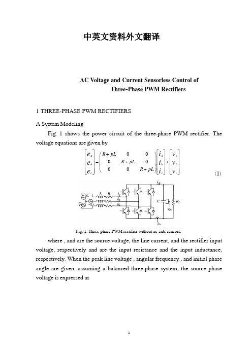
中英文资料外文翻译AC Voltage and Current Sensorless Control ofThree -Phase PWM Rectifiers1 THREE -PHASE PWM RECTIFIERSA System ModelingFig . 1 shows the power circuit of the three -phase PWM rectifier . The voltage equations are given by000000a a a b b b c c c R pL R pL R pL e i v e i v e i v ⎡⎤⎡⎤⎡⎤+⎛⎫⎢⎥⎢⎥⎢⎥ ⎪=++⎢⎥⎢⎥⎢⎥ ⎪⎢⎥⎢⎥⎢⎥ ⎪+⎝⎭⎢⎥⎢⎥⎢⎥⎣⎦⎣⎦⎣⎦ (1)Fig. 1. Three-phase PWM rectifier without ac-side sensors.where , and are the source voltage, the line current, and the rectifier input voltage, respectively and are the input resistance and the input inductance, respectively . When the peak line voltage , angular frequency , and initial phase angle are given, assuming a balanced three -phase system, the source phase voltage is expressed ascos 2cos()32cos()3a b c E e e e θθπθπ⎡⎤⎢⎥⎡⎤⎢⎥⎢⎥⎢⎥=-⎢⎥⎢⎥⎢⎥⎢⎥⎢⎥⎣⎦⎢⎥+⎣⎦ (2) Where0t θωθ=+ (3)A transformation matrix based on the estimated phase angle ,which transforms three -phase variables into a synchronous d –q reference frame, is23222cos cos()cos()323sin sin()sin()M M M M M M C θθπθπθθπθπ⎛⎫-+ ⎪ ⎪= ⎪++ ⎪⎝⎭ (4)Transforming (1) into the – reference frame using (4)qc qc qc M M dc dc dc e i v R pL L L R pL e i v ωω⎡⎤⎡⎤⎡⎤+-⎛⎫=+⎢⎥⎢⎥⎢⎥ ⎪+⎝⎭⎣⎦⎣⎦⎣⎦ (5)where p is a differential operator and .M M ωθ=Expressing (5) in a vector notationM e Ri LJi pLi v ω=+++ (6) where,qc dc e e e ⎡⎤=⎢⎥⎣⎦,qc dc i i i ⎡⎤=⎢⎥⎣⎦,qc dc v v v ⎡⎤=⎢⎥⎣⎦,0110J -⎛⎫= ⎪⎝⎭ (7) Taking a transformation of (2) by using (4)cos sin E e E θθ∆⎡⎤=⎢⎥∆⎣⎦ (8) WhereM θθθ∆=- (9)Expressing (6) and (8) in a discrete domain, by approximating the derivative term in (6) by a forward difference [9], respectively,[](1)(1)(1)()(1)(1)M e k Ri k LJi k L i k i k v k T ω-=-+-+--+- (10)c o s (1)(1)s i n (1)E k e k E k θθ∆-⎡⎤-=⎢⎥-∆-⎣⎦(11)Where T is the sampling period .Fig. 2. Overall control block diagram.B System ControlThe PI controllers are used to regulate the dc output voltage and the ac input current . For decoupling current control, the cross -coupling terms are compensated in a feed forward -typeand the source voltage is also compensated as a disturbance . For transient responses without overshoot, the anti -windup technique is employed [10]. The overall control block diagram eliminating the source voltage and line current sensors is shown in Fig . 2. The estimation algorithm of source voltages and line currents is described in the following sections .2 PREDICTIVE CURRENT ESTIMATIONThe currents of ()a I k and ()c I k can not be calculated instantly since the calculation time of the DSP is required . To eliminate the delay effect, a state observer can be used . In addition, the state observer provides the filtering effects for the estimated variable .Expressing (5) in a state -space form,x Ax Bu =+ (12) y Cx = (13) where,R L A R L ωω⎛⎫-- ⎪= ⎪ ⎪- ⎪⎝⎭,1010L B L ⎛⎫ ⎪= ⎪ ⎪ ⎪⎝⎭,1001C ⎛⎫= ⎪⎝⎭qc dc i x i ⎡⎤=⎢⎥⎣⎦,qc qc dc dc e v u e v -⎡⎤=⎢⎥-⎣⎦ And y is the output .Transforming (12) and (13) into a discrete domain, respectively,(1)()()X k FX k GU k +=+ (14)()()Y k HX k = (15)where,1111R T T L F R T T L ωω⎛⎫-- ⎪= ⎪ ⎪+- ⎪⎝⎭,00T L G T L ⎛⎫ ⎪= ⎪ ⎪ ⎪⎝⎭Then, the observer equation adding an error correction term to is given by(1)()()(()())X k F X k GU k K Y k Yk +=++- (16) Where K is the observer gain matrix and “^ ” means the estimated quantity, and (1)X k + is the state variable estimated ahead one sampling period . Subtracting (15) from (16), the error dynamic equation of the observer is expressed as(1)[]()rr rr e k F KC e k +=- (17) where ()()()rr e k X k X k =- . Here, it is assumed that the model parameters match well with the real ones . Fig . 3 shows the block diagram of the closed -loop state observer .The state variable error depends only on the initial error and is independent of the input . For (17) to converge to the zero state, the roots of the characteristic equation of (17) should be located within the unit circle .Fig. 3. Closed-loop state observer.Fig. 4. Short pulse region.4EXPERIMENTS AND DISCUSSIONSA. System Hardware ConfigurationFig. 5shows the system hardware configuration. The source voltage is a three-phase,110[V].The input resistance and inductance are0.06Ωand3.3 mH,respectively. The dc link capacitance is2350μF and the switching frequency of the PWM rectifier is3.5kHz.Fig. 5. System hardware configuration.Fig. 6. Dc link currents and corresponding phase currents (in sector V ).The TMS320C31DSP chip operating at33.3MHz is used as a main processor and two12-b A/D converters are used. One of them is dedicated for detecting the dc link current and the other is used for measuring the dc outputvoltage and the source voltages and currents,where ac side quantities are just measured for performance comparison.One of two internal timers in the DSP is employed to decide the PWM control period and the other is used to determine the dc link current interrupt. Considering the rectifier blanking time of3.5s,A/D conversion time of2.6s, and the other signal delay time,the minimum pulse width is set to10s.A.Experimental ResultsFig. 6shows measured dc link currents and phase currents. In case of sector V of the space vector diagram,the dc link current corresponds to for the switching state of and for that of . Fig. 7(a)shows the raw dc link current before filtering. It has a lot of ringing components due to the resonance of the leakage inductance and the snubber capacitor. When the dc current is sampled at the end point of the active voltage vectors as shown in the figure,the measuring error can be reduced.Fig. 7. Sampling of dc link currents.Fig. 8. Estimated source voltage and current at starting.To reduce this error further,the low pass filter should be employed,of which result is shown in Fig. 7(b). The cut-off frequency of the Butterworth’s second-order filter is112kHz and its delay time is about2sec. Since the ringing frequency is258kHz and the switching frequency is3.5[kHz],the filtered signal without significant delay is acquired.Fig. 8shows the estimated source voltage and current at starting. With the proposed initial estimation strategy,the starting operation is well performed. Fig. 9shows the phaseangle,magnitude,and waveform of the estimated source voltage,which coincide well with measured ones.Fig. 10shows the source voltage and current waveform at unity power factor. Figs. With the estimated quantities for the feedback control,the control performance is satisfactory. The dc voltage variation for load changes will be remarkably decreased if a feedforward control for theload current is added, which is possible without additional cur-rent sensor when the PWM rectifier is combined with the PWM inverter for ac motor drives.(a) phase angle (b)magnitude (c) waveform.Fig. 10. Source voltage and current waveforms.(a)estimated (b) measured.4 CONCLUSIONSThis paper proposed a novel control scheme of the PWM rectifiers without employing any ac input voltage and current sensors and with using dc voltage and current sensors only. Reducing the number of the sensors used decreases the system cost as well as improves the system reliability. The phase angle and the magnitude of the source voltage have been estimated bycontrolling the deviation between the rectifier current and its model current tobe zero. For line current reconstruction,switching states and measured dc link currents were used. To eliminate the effect of the calculation time delay of the microprocessor,the predictive state observer was used. It was shown that the estimation algorithm is robust to the parameter variation. The whole algorithm has been implemented for a proto-type1.5[kV A]PWM rectifier system controlled by TMS320C31DSP. The experimental results have verified that the proposed ac sensor elimination method is feasible.无交流电动势、电流传感器的三相PWM整流器控制1三相PWM整流器A 系统模型图一所示为三相PWM 整流器的主电路,电压等式给出如下:000000a a a b b b c c c R pL R pL R pL e i v e i v e i v ⎡⎤⎡⎤⎡⎤+⎛⎫⎢⎥⎢⎥⎢⎥ ⎪=++⎢⎥⎢⎥⎢⎥ ⎪⎢⎥⎢⎥⎢⎥ ⎪+⎝⎭⎢⎥⎢⎥⎢⎥⎣⎦⎣⎦⎣⎦ (1)图1 无交流传感器三相PWM 整流器其中e ,i 和v 分别是源电压,线电流和整流器的输入电压,R 和L 分别是输入电阻和输入电感。
外文文献翻译译稿和原文
外文文献翻译译稿1卡尔曼滤波的一个典型实例是从一组有限的,包含噪声的,通过对物体位置的观察序列(可能有偏差)预测出物体的位置的坐标及速度。
在很多工程应用(如雷达、计算机视觉)中都可以找到它的身影。
同时,卡尔曼滤波也是控制理论以及控制系统工程中的一个重要课题。
例如,对于雷达来说,人们感兴趣的是其能够跟踪目标。
但目标的位置、速度、加速度的测量值往往在任何时候都有噪声。
卡尔曼滤波利用目标的动态信息,设法去掉噪声的影响,得到一个关于目标位置的好的估计。
这个估计可以是对当前目标位置的估计(滤波),也可以是对于将来位置的估计(预测),也可以是对过去位置的估计(插值或平滑)。
命名[编辑]这种滤波方法以它的发明者鲁道夫.E.卡尔曼(Rudolph E. Kalman)命名,但是根据文献可知实际上Peter Swerling在更早之前就提出了一种类似的算法。
斯坦利。
施密特(Stanley Schmidt)首次实现了卡尔曼滤波器。
卡尔曼在NASA埃姆斯研究中心访问时,发现他的方法对于解决阿波罗计划的轨道预测很有用,后来阿波罗飞船的导航电脑便使用了这种滤波器。
关于这种滤波器的论文由Swerling(1958)、Kalman (1960)与Kalman and Bucy(1961)发表。
目前,卡尔曼滤波已经有很多不同的实现。
卡尔曼最初提出的形式现在一般称为简单卡尔曼滤波器。
除此以外,还有施密特扩展滤波器、信息滤波器以及很多Bierman, Thornton开发的平方根滤波器的变种。
也许最常见的卡尔曼滤波器是锁相环,它在收音机、计算机和几乎任何视频或通讯设备中广泛存在。
以下的讨论需要线性代数以及概率论的一般知识。
卡尔曼滤波建立在线性代数和隐马尔可夫模型(hidden Markov model)上。
其基本动态系统可以用一个马尔可夫链表示,该马尔可夫链建立在一个被高斯噪声(即正态分布的噪声)干扰的线性算子上的。
系统的状态可以用一个元素为实数的向量表示。
中值滤波器脉冲噪声中英文对照外文翻译文献
中英文资料外文翻译文献Improved 2-D Median Filter for On-Line Impulse Noise Suppressiom Abstract-An inproved 2-D median filter employing multishell concept to suppress impulse noise ,is presented.The performance of proposed filter is evaluated over image ‘LENA’,The impulsive noise is added using MATLAB utility.The modified strategy reduces the mnuber of replacement and results in better performance and simple hardware realization that is suitable for on-line implementation.Index terms-Median Filter , Multi-shell Median Filter, Impulse NoiseI.INTRODUCTIONIn TV and other imaging systems,impulse noise is a common impairment . The standard T.V.Broadcast signal is often contaminated with impulsive noise arising from various sources such as household electrical appliance and atmospheric disturbances.Broad banding of the signal further increases the level of impulsive noise. V arious filters are proposed to suppress such impairments[1].The median filter(MF)[1-2] is widely usedfor impulse noise suppression and the multishell median filter(MMF)[3] introduces the concept of missing line recovery. Although these filters have satisfactory performance, MMF failsto filter two impulse noises in the same prossing window. Moveover,these filters tend to blur the images due to too many replacements. C.J.Juan proposed a modified multishell median filter (MMMF)[4], which removes most of the shortcomings associated with the MF and the MMF. However, it is observed that under certain condions, to be discussed in the follow sections, MMMF fails to perform the desired filtering operation .Moreover,the number of calculations/replacements invoved on the basis of MIN/MAX conditions is still too large and makes the filter difficult to realize,particulariy for real time applications.In this paper, the threshold strtegy of MMMF is modified so that:(a)effective noise filtering operations are performed under allconditions,and(b)number of calculations/replacements is reduced and simplified. This results in a simple hardware realization of the filter.II.PROPOSED MODIFICATIONConsider a 3x3-processing window, with P5 as the central pixel,as shown in Figure 1.P1 P2 P3P4 P5 P6P7 P8 P9Fig.1. A 3x3 processing windowThe output of MMMF as proposed in [4] isOutput (X,Y)= Max(P2,P8)if P5﹥Max[S]P5 if Min [s]﹤Max[S]Min(P2,P8) if P5﹤Max[S] (1)Where S is the set of samples surrounding central pixels except(P4.P6)i.e.S={P1,P2,P3,P7,P8,P9} (2) The principle invoved in the replacement strategy of Equation(1) is that if P5 is corrupted by noise ,it is better to replaceits gray level by P2 or P8 than by using Min[S] orMax[S] .also,due to missing lines error,since P4 and P6 may belost, they are not considered in Equation(2).The limitation of Equation(1) is that when Min[S] or Max[S] arealso corrupted by impulse noise,i.e.either Min[S] or Max[S] isequal to P5,Equation(1)fails to perform the desired filtering operation.To overcome this limitation following modificationsin the replacement strategy of Equation(1),are proposed.Output (X,Y)= Max(P2,P8)if P5≥Max[S]P5 if Min [s]<P5<Max[S] Min(P2,P8) if P5≤Max[S] (3)It has been observed that more than 70-80% points in an image,the gray level diatances of P5 from(P2 or P8) and from Max[S] are below 16.This is shown in Fig.2 for the image ‘LENA’.This fact is used to further reduce unnessary replacements,thereby reducing the bluring of the images.Thus taking into considertion of Figure(3) can be further modified asOutput (X,Y)= Max(P2,P8)if P5-Max[S]≥16Max(P2,P8) if Min [s]-P5≥16P5 otherwise (4)Equation 4 indicates that replacing action takes place only when the distance between P5 and Min[S] or Max[S] is no smaller than 16. This strtegy thus avoids the necessary replacements and reduces blurring of the images.Moreover,it can be implemented using simple comparators and subtractors.Gray level distancesFig.2. Gray level distances between central point and its neighboring points for the image ‘LENNA’Ⅲ .RESULTSFigure 3 shows the original image ‘LENNA’and Figure 4 shows the same image when corrupted with impulse noise. Results of median filter and the proposed filter are given in Figures 5 and 6, paring Figures 5 and 6, it is observed that the result of the proposed filter is much better than those obtained using the median filter. Aithough,the median filter remove the impulsive moise effectively, however,the image gets blurred.The proposed filter removes the impulsive noise and also preserves the details of the image.A multishell filter employing the modified replacement strategy is presentde in this paper.The modified filter effectively suppresses the inpulse moise.It uses threshold conditions that require fewer comparisons and replacements and is faster as compared to the other multishell median filters.moreover,it can be realized using simple comparators and subtractors and subtractors and hence can be effectively used in real time applications改进二维中值滤波器在线脉冲噪声的抑制摘要:一种改进二维中值滤波器,采用多壳的概念,以抑制脉冲噪声,拟定的过滤器的性能进行评估超过图像“LENNA”的中值滤波,脉冲噪声被添加使用到MATLAB的实用工具中。
电子信息工程专业外文翻译--滤波器

外文原文一、a question for study or discussion1.Research background and purpose1.1 conceptualizeElliptic filter (Elliptic filter), also known as the Call filter (Cauer filter), is in the passband and stopband ripple of a filter. Elliptic filter when compared to other types of filters, in order under the same conditions with minimal fluctuations in the passband and stopband. Same as its wave in passband and stopband, which distinguish it from the Butterworth filter with flat passband and stopband and flat passband and the stopband ripple or resistance with flat, cut than the snow filter passband ripple.A low-pass filter with a frequency response range of the ellipse:Four-order low-pass elliptic filter frequency response。
1.2 scientific researchIn the low-frequency (600Hz=500KHz) commonly used in band-pass filter, large LC filters, poor stability, stability of Crystal filters, but can only be made of narrow-band filter, bad shock and vibration resistance. Active filters are small, but stability and decay characteristics are often poor, and debugging easy. Ceramic filter is poor and low-frequency seismic performance of low temperature coefficient. And than snow filter Butterworth filter transfer function is a polynomial divided by a constant, for the whole network, all zeros in infinite, only infinite stopband attenuation is infinite, and the elliptic filter in both with zeros and poles on the limited frequency. Zero ripple in the passband, that it has a minimum across the passband and stopband ripple, This is distinguished from Butterworth filter with flat passband and stopband。
【最新推荐】基于DSP的IIR滤波器设计外文文献
学科分类号本科毕业设计题目(中文):基于DSP的IIR滤波器设计(英文):The Design of IIR Filter Basedon DSP Chip姓名学号院(系)专业、年级指导教师二〇年月目录摘要 (1)Abstract. (2)1 绪论 (2)1.1 认识数字信号处理和IIR数字滤波器 (3)1.2 数字滤波器的实现方法 (4)1.3 主要研究内容 (6)2 滤波器原理基础 (6)2.1 IIR数字滤波器的优缺点 (7)2.2 IIR数字滤波器的设计方法和原理 (9)2.2.1 脉冲响应不变法 (12)2.2.2 双线性变换法 (14)2.3 IIR滤波器的基本结构 (17)3 IIR滤波器的设计过程及DSP的实现 (21)3.1 IIR滤波器的设计过程 (21)3.2 DSP系统的设计流程 (22)3.3 IIR数字滤波器在DSP上的实现 (22)参考文献 (27)附录 (28)致谢 (31)外文文献译文......................................................................................... 1-3 外文文献原文基于DSP的IIR滤波器设计摘要:数字信号处理(Digital Signal Processing,DSP)是一门涉及许多学科而又广泛应用于众多领域的新兴学科。
早在20世纪60年代,数字信号处理(即信号的数字化及数字处理)理论已经被被提出,到20世纪70年代,DSP理论和算法基础才被人提出。
不久之后,1982年世界上第一枚DSP芯片诞生了。
这枚DSP芯片在当时运算速度很快,尤其是在编码解码和语音合成方面得到广泛应用。
随着科学技术的飞速发展,数字化硬件技术得到长足的发展,这就带动了数字信号处理的飞速发展,也使得它得到了很多的实际应用,由此奠定了DSP这一词的地位。
之后,DSP芯片的科研不断推陈出新,每一代的DSP芯片都向着使运算速度更快、精度更高的目标发展,应用于通信、语音、医疗、仪器仪表和家用电器等人类生产生活的各个领域。
外文翻译--数字滤波器的仿真与实现

毕业设计(论文)外文资料翻译院系电子信息工程专业电子信息工程学生姓名班级学号外文出处百度文库附件:1.外文资料翻译译文(约3000汉字);2.外文资料原文(与课题相关的1万印刷符号左右)。
英文原文The simulation and the realization of the digital filter With the information age and the advent of the digital world, digital signal processing has become one of today's most important disciplines and door technology. Digital signal processing in communications, voice, images, automatic control, radar, military, aerospace, medical and household appliances, and many other fields widely applied. In the digital signal processing applications, the digital filter is important and has been widely applied.1、figures Unit on :Analog and digital filtersIn signal processing, the function of a filter is to remove unwanted parts of the signal, such as random noise, or to extract useful parts of the signal, such as the components lying within a certain frequency range.The following block diagram illustrates the basic idea.There are two main kinds of filter, analog and digital. They are quite different in their physical makeup and in how they work. An analog filter uses analog electronic circuits made up from components such as resistors, capacitors and op amps to produce the required filtering effect. Such filter circuits are widely used in such applications as noise reduction, video signal enhancement, graphic equilibrium in hi-fi systems, and many other areas. There are well-established standard techniques for designing an analog filter circuit for a given requirement. At all stages, the signal being filtered is an electrical voltage or current which is the direct analogue of the physical quantity (e.g. a sound or video signal or transducer output) involved. A digital filter uses a digital processor to performnumerical calculations on sampled values of the signal. The processor may be a general-purpose computer such as a PC, or a specialized DSP (Digital Signal Processor) chip. The analog input signal must first be sampled and digitized using an ADC (analog to digital converter). The resulting binary numbers, representing successive sampled values of the input signal, are transferred to the processor, which carries out numerical calculations on them. These calculations typically involve multiplying the input values by constants and adding the products together. If necessary, the results of these calculations, which now represent sampled values of the filtered signal, are output through a DAC (digital to analog converter) to convert the signal back to analog form.Note that in a digital filter, the signal is represented by a sequence of numbers, rather than a voltage or current.The following diagram shows the basic setup of such a system.Unit refers to the input signals used to filter hardware or software. If the filter input, output signals are separated, they are bound to respond to the impact of the Unit is separated, such as digital filters filter definition. Digital filter function, which was to import sequences X transformation into export operations through a series Y.According to figures filter function 24-hour live response characteristics, digital filters can be divided into two, namely, unlimited long live long live the corresponding IIR filter and the limited response to FIR filters. IIR filters have theadvantage of the digital filter design can use simulation results, and simulation filter design of a large number of tables may facilitate simple. It is the shortcomings of the nonlinear phase; Linear phase if required, will use the entire network phase-correction. Image processing and transmission of data collection is required with linear phase filters identity. And FIR linear phase digital filter to achieve, but an arbitrary margin characteristics. Impact from the digital filter response of the units can be divided into two broad categories : the impact of the limited response (FIR) filters, and unlimited number of shocks to (IIR) digital filters.FIR filters can be strictly linear phase, but because the system FIR filter function extremity fixed at the original point, it can only use the higher number of bands to achieve their high selectivity for the same filter design indicators FIR filter called band than a few high-IIR 5-10 times, the cost is higher, Signal delay is also larger. But if the same linear phase, IIR filters must be network-wide calibration phase, the same section also increase the number of filters and net work complexity. FIR filters can be used the recursive method, not in a limited precision of a shock, and into the homes and quantitative factors of uncertainty arising from the impact of errors than IIR filter small number, and FIR filter can be used FFT algorithms, the computational speed. But unlike IIR filter can filter through the simulation results, there is no ready-made formula FIR filter must use computer-aided design software (such as MATLAB) to calculate. So, a broader application of FIR filters, and IIR filters are not very strict requirements on occasions.Unit from sub-functions can be divided into the following four categories :(1) Low-filter (LPF);(2) high-filter (HPF);(3) belt-filter (BPF);(4) to prevent filter (BSF).The following chart dotted line for the ideals of the filter frequency characteristics :2、MATLAB introducedMATLAB is a matrix laboratory (Matrix Laboratory) is intended. In addition to an excellent value calculation capability, it also provides professional symbols terms, word processing, visualization modeling, simulation and real-time control functions. MATLAB as the world's top mathematical software applications, with a strong engineering computing, algorithms research, engineering drawings, applications development, data analysis and dynamic simulation, and other functions, in aerospace, mechanical manufacturing and construction fields playing an increasingly important role. And the C language function rich, the use of flexibility, high-efficiency goals procedures. High language both advantages aswell as low level language features. Therefore, C language is the most widely used programming language. Although MATLAB is a complete, fully functional programming environment, but in some cases, data and procedures with the external environment of the world is very necessary and useful. Filter design using MATLAB, could be adjusted with the design requirements and filter characteristics of the parameters, visual simple, greatly reducing the workload for the filter design optimization.In the electricity system protection and secondary computer control, many signal processing and analysis are based on are certain types sinusoidal wave and the second harmonics of the system voltage and current signals (especially at D process), are mixed with a variety of complex components, the filter has been installed power system during the critical components. Current computer protection and the introduction of two digital signal processing software main filter. Digital filter design using traditional cumbersome formula, the need to change the parameters after recalculation, especially in high filters, filter design workload. Uses MATLAB signal processing boxes can achieve rapid and effective digital filter design and simulation.MATLAB is the basic unit of data matrix, with its directives expression mathematics, engineering, commonly used form is very similar, it is used to solve a problem than in MATLAB C, Fortran and other languages End precision much the same thing. The popular MATLAB 5.3/Simulink3.0 including hundreds of internal function with the main pack and 30 types of tool kits (Toolbox). kits can be divided into functional tool kits and disciplines toolkit. MATLAB tool kit used to expand the functional symbols terms, visualization modeling simulation, word processing and real-time control functions. professional disciplines toolkit is a stronger tool kits, tool kits control, signal processing tool kit, tool kits, etc. belonging to such communicationsMATLAB users to open widely welcomed. In addition to the internal function, all the packages MATLAB tool kits are readable document and the document could be amended, modified or users through original program the construction of new procedures to prepare themselves for kits.3、Digital filter designDigital filter design of the basic requirementsDigital filter design must go through three steps :(1) Identification of indicators : In the design of a filter, there must be some indicators. These indicators should be determined on the basis of the application. In many practical applications, digital filters are often used to achieve the frequency operation. Therefore, indicators in the form of general jurisdiction given frequency range and phase response. Margins key indicators given in two ways. The first is absolute indicators. It provides a function to respond to the demands of the general application of FIR filter design. The second indicator is the relative indicators. Its value in the form of answers to decibels. In engineering practice, the most popular of such indicators. For phase response indicators forms, usually in the hope that the system with a linear phase frequency bands human. Using linear phase filter design with the following response to the indicators strengths:①it only contains a few algorithms, no plural operations;②there is delay distortion, only a fixed amount of delay; ③the filter length N (number of bands for N-1), the volume calculation for N/2 magnitude.(2) Model approach : Once identified indicators can use a previous study of the basic principles and relationships, a filter model to be closer to the target system.(3) Achieved : the results of the above two filters, usually by differential equations, system function or pulse response to describe. According to this description of hardware or software used to achieve it.4、Introduction of DSPToday, DSP is widely used in the modern techno logy and it has been the key part of many products and played more and mo re important role in our daily life Recently, Northwestern Poly technical University Aviation Microelectronic Center has completed the design of digital signal processor co re NDSP25, which is aiming at TM S320C25 digital signal processor of Texas Instrument TM S320 series. By using top 2dow n design flow NDSP25 is compatible with instruction and interface timing of TM S320C25.Digital signal processors (DSP) is a fit for real-time digital signal processing for high-speed dedicated processors, the main variety used for real-time digital signal processing to achieve rapid algorithms. In today's digital age background, the DSP has become the communications, computer, and consumer electronics products, and other fields based device.Digital signal processors and digital signal processing is inseparably, we usually say "DSP" can also mean the digital signal processing (Digital Signal Processing), is that in this digital signal processors Lane. Digital signal processing is a cover many disciplines applied to many areas and disciplines, refers to the use of computers or specialized processing equipment, the signals in digital form for the collection, conversion, recovery, valuation, enhancement, compression, identification, processing, the signals are compliant form. Digital signal processors for digital signal processing devices, it is accompanied by a digital signal processing to produce. DSP development process is broadly divided into three phases : the 20th century to the 1970s theory that the 1980s and 1990s for the development of products. Before the emergence of the digital signal processing in the DSP can only rely on microprocessors (MPU) to complete. However, the advantage of lower high-speed real-time processing can not meet the requirements. Therefore, until the 1970s, a talent made based DSP theory and algorithms. With LSI technology development in 1982 was the first recipient of the world gave birth to the DSP chip. Years later, the second generation based on CMOS工艺DSP chips have emerged. The late 1980s, the advent of the third generation of DSP chips. DSP is the fastest-growing 1990s, there have been four successive five-generation and the generation DSP devices. After 20 years of development, the application of DSP products has been extended to people's learning, work and all aspects of life and gradually become electronics products determinants.中文翻译数字滤波器的仿真与实现随着信息时代和数字世界的到来,数字信号处理已成为当今一门极其重要的学科和技术领域。
滤波器英文
The simulation and the realization of the digital filterWith the information age and the advent of the digital world, digital signal processing has become one of today's most important disciplines and door technology. Digital signal processing in communications, voice, images, automatic control, radar, military, aerospace, medical and household appliances, and many other fields widely applied. In the digital signal processing applications, the digital filter is important and has been widely applied.1、figures Unit on :Analog and digital filtersIn signal processing, the function of a filter is to remove unwanted parts of the signal, such as random noise, or to extract useful parts of the signal, such as the components lying within a certain frequency range.The following block diagram illustrates the basic idea.There are two main kinds of filter, analog and digital. They are quite different in their physical makeup and in how they work. An analog filter uses analog electronic circuits made up from components such as resistors, capacitors and op amps to produce the required filtering effect. Such filter circuits are widely used in such applications as noise reduction, video signal enhancement, graphic equalisers in hi-fi systems, and many other areas. There are well-established standard techniques for designing an analog filter circuit for a given requirement. At all stages, the signal being filtered is an electrical voltage or current which is the direct analogue of the physical quantity (e.g. a sound or video signal or transducer output) involved. A digital filter uses a digital processor to perform numerical calculations on sampled values of the signal. The processor may be a general-purpose computer such as a PC, or a specialised DSP (Digital Signal Processor) chip. The analog input signal must first be sampled and digitised using an ADC (analog to digital converter). The resulting binary numbers, representing successive sampled values of the input signal, are transferred to the processor, which carries out numerical calculations on them. These calculations typically involve multiplying the input values by constants and adding the products together. If necessary, theresults of these calculations, which now represent sampled values of the filtered signal, are output through a DAC (digital to analog converter) to convert the signal back to analog form.Note that in a digital filter, the signal is represented by a sequence of numbers, rather than a voltage or current.The following diagram shows the basic setup of such a system.Unit refers to the input signals used to filter hardware or software. If the filter input, output signals are separated, they are bound to respond to the impact of the Unit is separated, such as digital filters filter definition. Digital filter function, which was to import sequences X transformation into export operations through a series Y.According to figures filter function 24-hour live response characteristics, digital filters can be divided into two, namely, unlimited long live long live the corresponding IIR filter and the limited response to FIR filters. IIR filters have the advantage of the digital filter design can use simulation results, and simulation filter design of a large number of tables may facilitate simple. It is the shortcomings of the nonlinear phase; Linear phase if required, will use the entire network phase-correction. Image processing and transmission of data collection is required with linear phase filters identity. And FIR linear phase digital filter to achieve, but an arbitrary margin characteristics. Impact from the digital filter response of the units can be divided into two broad categories : the impact of the limited response (FIR) filters, and unlimited number of shocks to (IIR) digital filters.FIR filters can be strictly linear phase, but because the system FIR filter function extremity fixed at the original point, it can only use the higher number of bands to achieve their highselectivity for the same filter design indicators FIR filter called band than a few high-IIR 5-10 times, the cost is higher, Signal delay is also larger. But if the same linear phase, IIR filters must be network-wide calibration phase, the same section also increase the number of filters and network complexity. FIR filters can be used to achieve non-Digui way, not in a limited precision of a shock, and into the homes and quantitative factors of uncertainty arising from the impact of errors than IIR filter small number, and FIR filter can be used FFT algorithms, the computational speed. But unlike IIR filter can filter through the simulation results, there is no ready-made formula FIR filter must use computer-aided design software (such as MATLAB) to calculate. So, a broader application of FIR filters, and IIR filters are not very strict requirements on occasions.Unit from sub-functions can be divided into the following four categories :(1) Low-filter (LPF);(2) high-filter (HPF);(3) belt-filter (BPF);(4) to prevent filter (BSF).The following chart dotted line for the ideals of the filter frequency characteristics :A1(f) A2(f)10 f2cf 0 f2cf(a) (b)A3(f) A4(f)0 f1cf2cf 0 f1cf2cf(c) (d)(a)LPF (b)HPF (c)BPF (d)BSF2、MATLAB introducedMATLAB is a matrix laboratory (Matrix Laboratory) is intended. In addition to an excellent value calculation capability, it also provides professional symbols terms, word processing, visualization modeling, simulation and real-time control functions. MATLAB as the world's top mathematical software applications, with a strong engineering computing, algorithms research, engineering drawings, applications development, data analysis and dynamic simulation, and other functions, in aerospace, mechanical manufacturing and construction fields playing an increasingly important role. And the C language function rich, the use of flexibility, high-efficiency goals procedures. High language both advantages as well as low level language features. Therefore, C language is the most widely used programming language. Although MATLAB is a complete, fully functional programming environment, but in some cases, data and procedures with the external environment of the world is very necessary and useful. Filter design using Matlab, could be adjusted with the design requirements and filter characteristics of the parameters, visual simple, greatly reducing the workload for the filter design optimization.In the electricity system protection and secondary computer control, many signal processing and analysis are based on are certain types Yeroskipou and the second harmonics of the system voltage and current signals (especially at D process), are mixed with a variety of complex components, the filter has been installed power system during the critical components. Current computer protection and the introduction of two digital signal processing software main filter. Digital filter design using traditional cumbersome formula, the need to change the parameters after recalculation, especially in high filters, filter design workload. Uses MATLAB signal processing boxes can achieve rapid and effective digital filter design and simulation.MATLAB is the basic unit of data matrix, with its directives Biaodashi mathematics, engineering, commonly used form is very similar, it is used to solve a problem than in MATLAB C, Fortran and other languages End precision much the same thing. The popular MATLAB 5.3/Simulink3.0 including hundreds of internal function with the main pack and 30 types of tool kits (Toolbox). kits can be divided into functional tool kits and disciplines toolkit. MATLAB tool kit used to expand the functional symbols terms, visualization simulationmodelling, word processing and real-time control functions. professional disciplines toolkit is a stronger tool kits, tool kits control, signal processing tool kit, tool kits, etc. belonging to such communicationsMATLAB users to open widely welcomed. In addition to the internal function, all the packages MATLAB tool kits are readable document and the document could be amended, modified or users through Yuanchengxu the construction of new procedures to prepare themselves for kits.3、Digital filter designDigital filter design of the basic requirementsDigital filter design must go through three steps :(1) Identification of indicators : In the design of a filter, there must be some indicators. These indicators should be determined on the basis of the application. In many practical applications, digital filters are often used to achieve the frequency operation. Therefore, indicators in the form of general jurisdiction given frequency range and phase response. Margins key indicators given in two ways. The first is absolute indicators. It provides a function to respond to the demands of the general application of FIR filter design. The second indicator is the relative indicators. Its value in the form of answers to decibels. In engineering practice, the most popular of such indicators. For phase response indicators forms, usually in the hope that the system with a linear phase frequency bands human. Using linear phase filter design with the following response to the indicators strengths:①it only contains a few algorithms, no plural operations;②there is delay distortion, only a fixed amount of delay; ③the filter length N (number of bands for N-1), the volume calculation for N/2 magnitude.(2) Model approach : Once identified indicators can use a previous study of the basic principles and relationships, a filter model to be closer to the target system.(3) Achieved : the results of the above two filters, usually by differential equations, system function or pulse response to describe. According to this description of hardware or software used to achieve it.4、Introduced FPGAProgrammable logic device is a generic logic can use a variety of chips, which is to achieve ASIC ASIC (Application Specific Integrated Circuit) semi-customized device, Its emergenceand development of electronic systems designers use CAD tools to design their own laboratory in the ASIC device. Especially FPGA (Field Programmable Gate Array) generated and development, as a microprocessor, memory, the figures for electronic system design and set a new industry standard (that is based on standard product sales catalogue in the market to buy). Is a digital system for microprocessors, memories, FPGA or three standard building blocks constitute their integration direction.Digital circuit design using FPGA devices, can not only simplify the design process and can reduce the size and cost of the entire system, increasing system reliability. They do not need to spend the traditional sense a lot of time and effort required to create integrated circuits, to avoid the investment risk and become the fastest-growing industries of electronic devices group. Digital circuit design system FPGA devices using the following main advantages(1)Design flexibleUse FPGA devices may not in the standard series device logic functional limitations. And changes in system design and the use of logic in any one stage of the process, and only through the use of re-programming the FPGA device can be completed, the system design provides for great flexibility.(2) Increased functional densityFunctional density in a given space refers to the number of functional integration logic. Programmable logic chip components doors several high, a FPGA can replace several films, film scores or even hundreds of small-scale digital IC chip illustrated in the film. FPGA devices using the chip to use digital systems in small numbers, thus reducing the number of chips used to reduce the number of printed size and printed, and will ultimately lead to a reduction in the overall size of the system.(3) Improve reliabilityPrinting plates and reduce the number of chips, not only can reduce system size, but it greatly enhanced system reliability. A higher degree of integration than systems in many low-standard integration components for the design of the same system, with much higher reliability. FPGA device used to reduce the number of chips required to achieve the system in the number printed on the cord and joints are reduced, the reliability of the system can be improved.(4) Shortening the design cycleAs FPGA devices and the programmable flexibility, use it to design a system for longer than traditional methods greatly shortened. FPGA device master degrees high, use printed circuit layout wiring simple. At the same time, success in the prototype design, the development of advanced tools, a high degree of automation, their logic is very simple changes quickly. Therefore, the use of FPGA devices can significantly shorten the design cycle system, and speed up the pace of product into the market, improving product competitiveness.(5) Work fastFPGA/CPLD devices work fast, generally can reach several original Hertz, far larger than the DSP device. At the same time, the use of FPGA devices, the system needed to achieve circuitclasses and small, and thus the pace of work of the entire system will be improved.(6) Increased system performance confidentialityMany FPGA devices have encryption functions in the system widely used FPGA devices can effectively prevent illegal copying products were others(7) To reduce costsFPGA device used to achieve digital system design, if only device itself into the price, sometimes you would not know it advantages, but there are many factors affecting the cost of the system, taken together, the cost advantages of using FPGA is obvious. First, the use of FPGA devices designed to facilitate change, shorten design cycles, reduce development costs for system development; Secondly, the size and FPGA devices allow automation needs plug-ins, reducing the manufacturing system to lower costs; Again, the use of FPGA devices can enhance system reliability, reduced maintenance workload, thereby lowering the cost of maintenance services for the system. In short, the use of FPGA devices for system design to save costs.FPGA design principles :FPGA design an important guiding principles : the balance and size and speed of exchange, the principles behind the design of the filter expression of a large number of certification.Here, "area" means a design exertion FPGA/CPLD logic resources of the FPGA can be used to the typical consumption (FF) and the search table (IUT) to measure more general measure can be used to design logic equivalence occupied by the door is measured. "pace" means stability operations in the chip design can achieve the highest frequency, the frequency of the time series design situation, and design to meet the clock cycle -- PADto pad, Clock SetupTime, Clock Hold Beijing, Clock-to-Output Delay, and other characteristics of many time series closely related. Area (area) and speed (speed) runs through the two targets FPGA design always is the ultimate design quality evaluation criteria. On the size and speed of the two basic concepts : balance of size and speed and size and speed of swap.One pair of size and speed is the unity of opposites contradictions body. Requirements for the design of a design while the smallest, highest frequency of operation is unrealistic. More scientific goal should be to meet the design requirements of the design time series (includes requirements for the design frequency) premise, the smallest chip area occupied. Or in the specified area, the design time series cushion greater frequency run higher. This fully embodies the goals of both size and speed balanced thinking. On the size and speed requirements should not be simply interpreted as raising the level and design engineers perfect sexual pursuit, and should recognize that they are products and the quality and cost of direct relevance. If time series cushion larger design, running relatively high frequency, that the design Jianzhuangxing stronger, more quality assurance system as a whole; On the other hand, the smaller size of consumption design is meant to achieve in chip unit more functional modules, the chip needs fewer, the entire system has been significantly reduced cost. As a contradiction of the two components, the size and speed is not the same status. In contrast, meet the timetables and work is more important for some frequency when both conflicts, the use of priority guidelines.Area and the exchange rate is an important FPGA design ideas. Theoretically, if a design time series cushion larger, can run much higher than the frequency design requirements, then we can through the use of functional modules to reduce the consumption of the entire chip design area, which is used for space savings advantages of speed; Conversely, if the design of a time series demanding, less than ordinary methods of design frequency then generally flow through the string and data conversion, parallel reproduction of operational module, designed to take on the whole "string and conversion" and operate in the export module to chip in the data "and string conversion" from the macro point of view the whole chip meets the requirements of processing speed, which is equivalent to the area of reproduction - rate increase.For example. Assuming that the digital signal processing system is 350Mb/s input data flow rate, and in FPGA design, data processing modules for maximum processing speed of 150Mb/s, because the data throughput processing module failed to meet requirements, it is impossible to achieve directly in the FPGA. Such circumstances, they should use"area-velocity" thinking, at least three processing modules from the first data sets will be imported and converted, and then use these three modules parallel processing of data distribution, then the results "and string conversion," we have complete data rate requirements. We look at both ends of the processing modules, data rate is 350Mb/s, and in view of the internal FPGA, each sub-module handles the data rate is 150Mb/s, in fact, all the data throughput is dependent on three security modules parallel processing subsidiary completed, that is used by more chip area achieve high-speed processing through "the area of reproduction for processing speed enhancement" and achieved design.FPGA is the English abbreviation Field of Programmable Gate Array for the site programmable gate array, which is in Pal, Gal, Epld, programmable device basis to further develop the product. It is as ASIC (ASIC) in the field of a semi-customized circuit and the emergence of both a customized solution to the shortage circuit, but overcome the original programmable devices doors circuit few limited shortcomings.FPGA logic module array adopted home (Logic Cell Array), a new concept of internal logic modules may include CLB (Configurable Logic Block), export import module IOB (Input Output Block) and internal links (Interconnect) 3. FPGA basic features are :(1) Using FPGA ASIC design ASIC using FPGA circuits, the chip can be used,while users do not need to vote films production.(2) FPGA do other customized or semi-customized ASIC circuits throughout the Chinese specimen films.3) FPGA internal capability and rich I/O Yinjue.4) FPGA is the ASIC design cycle, the shortest circuit, the lowest development costs, risks among the smallest device5) FPGA using high-speed Chmos crafts, low consumption, with CMOS, TTL low-power compatibleIt can be said that the FPGA chip is for small-scale systems to improve system integration, reliability one of the bestCurrently FPGA many varieties, the Revenue software series, TI companies TPC series, the fiex ALTERA company seriesFPGA is stored in films from the internal RAM procedures for the establishment of the state of its work, therefore, need to programmed the internal Ram. Depending on the differentconfiguration, users can use a different programming methodsPlus electricity, FPGA, EPROM chips will be read into the film, programming RAM中data, configuration is completed, FPGA into working order. Diaodian, FPGA resume into white films, the internal logic of relations disappear, FPGA to repeated use. FPGA's programming is dedicated FPGA programming tool, using generic EPROM, prom programming device can. When the need to modify functional FPGA, EPROM can only change is. Thus, with a FPGA, different programming data to produce different circuit functions. Therefore, the use of FPGA very flexible.There are a variety of FPGA model : the main model for a parallel FPGA plus a EPROM manner; From the model can support a number of films FPGA; serial prom programming model could be used serial prom FPGA programming FPGA; The external model can be engineered as microprocessors from its programming microprocessors.Verilog HDL is a hardware description language for the algorithm level, doors at the level of abstract level to switch-level digital system design modelling. Modelling of the target figure by the complexity of the system can be something simple doors and integrity of electronic digital systems. Digital system to the levels described, and in the same manner described in Hin-time series modelling.Verilog HDL language with the following description of capacity : design behaviour characteristics, design data flow characteristics, composition and structure designed to control and contain the transmission and waveform design a certification mechanism. All this with the use of a modelling language. In addition, Verilog HDL language programming language interface provided by the interface in simulation, design certification from the external design of the visit, including specific simulation control and operation.Verilog HDL language grammar is not only a definition, but the definition of each grammar structure are clear simulation, simulation exercises. Therefore, the use of such language to use Verilog simulation models prepared by a certification. From the C programming language, the language inherited multiple operating sites and structures. Verilog HDL provides modelling capacity expansion, many of the initial expansion would be difficult to understand. However, the core subsets of Verilog HDL language very easy to learn and use, which is sufficient for most modelling applications. Of course, the integrity of the hardware description language is the most complex chips from the integrity of the electronic systems described.historyVerilog HDL language initially in 1983 by Gateway Design Automation companies for product development simulator hardware modelling language. Then it is only a dedicated language. Since their simulation, simulation devices widely used products, Verilog HDL as a user-friendly and practical language for many designers gradually accepted. In an effort to increase the popularity of the language activities, Verilog HDL language in 1990 was a public area. Open Verilog International (OVI) is to promote the development of Verilog international organizations. 1992, decided to promote OVI OVI standards as IEEE Verilog standards. The effort will ultimately succeed, a IEEE1995 Verilog language standard, known as IEEE Std 1364-1995. Integrity standards in Verilog hardware description language reference manual contains a detailed description.Main capacity:Listed below are the main Verilog hardware description language ability*Basic logic gate, and, for example, or have embedded in the language and nand* Users of the original definition of the term (UDP), the flexibility. Users can be defined in the original language combinations logic original language, the original language of logic could also be time series* Switches class infrastructure models, such as the nmos and pmos also be embedded in the language* Hin-language structure designated for the cost of printing the design and trails Shi Shi and design time series checks.* Available three different ways to design or mixed mode modelling. These methods include : acts described ways - use process of structural modelling; Data flow approach - use of a modelling approach Fuzhi expression; Structured way - using examples of words to describe modular doors and modelling.* Verilog HDL has two types of data : data types and sequence data line network types. Line network types that the physical links between components and sequence types that abstract data storage components.* To describe the level design, the structure can be used to describe any level module example * Design size can be arbitrary; Language is design size (size) impose any restrictions* Verilog HDL is no longer the exclusive language of certain companies but IEEE standards.* And the machine can read Verilog language, it may as EDA tools and languages of the world between the designers* Verilog HDL language to describe capacity through the use of programming language interface (PLI) mechanism further expansion. PLI is to allow external functions of the visit Verilog module information, allowing designers and simulator world Licheng assembly* Design to be described at a number of levels, from the switch level, doors level, register transfer level (RTL) to the algorithm level, including the level of process and content* To use embedded switching level of the original language in class switch design integrity modelling* Same language can be used to generate simulated incentive and certification by the designated testing conditions, such as the value of imports of the designated*Verilog HDL simulation to monitor the implementation of certification, the certification process of implementing the simulation can be designed to monitor and demonstrate value. These values can be used to compare with the expectations that are not matched in the case of print news reports.* Acts described in the class, not only in the RTL level Verilog HDL design description, and to describe their level architecture design algorithm level behavioural description* Examples can use doors and modular structure of language in a class structure described* Verilog HDL mixed mode modelling capabilities in the design of a different design in each module can level modelling* Verilog HDL has built-in logic function, such as*Structure of high-level programming languages, such as conditions of expression, and the cycle of expression language, language can be used* To it and can display regular modelling* Provide a powerful document literacy* Language in the specific circumstances of non-certainty that in the simulator, different models can produce different results; For example, describing events in the standard sequence of events is not defined.5、In troduction of DSPToday, DSP is w idely used in the modern techno logy and it has been the key part of many p roducts and p layed more and mo re impo rtant ro le in our daily life.Recent ly, Northw esternPo lytechnica lUniversity Aviation Microelect ronic Center has comp leted the design of digital signal signal p rocesso r co re NDSP25, w h ich is aim ing at TM S320C25 digital signal p rocesso r of Texas Inst rument TM S320 series. By using top 2dow n design flow , NDSP25 is compat ible w ith inst ruct ion and interface t im ing of TM S320C25.Digital signal processors (DSP) is a fit for real-time digital signal processing for high-speed dedicated processors, the main variety used for real-time digital signal processing to achieve rapid algorithms. In today's digital age background, the DSP has become the communications, computer, and consumer electronics products, and other fields based device.Digital signal processors and digital signal processing is inseparably, we usually say "DSP" can also mean the digital signal processing (Digital Signal Processing), is that in this digital signal processors Lane. Digital signal processing is a cover many disciplines applied to many areas and disciplines, refers to the use of computers or specialized processing equipment, the signals in digital form for the collection, conversion, recovery, valuation, enhancement, compression, identification, processing, the signals are compliant form. Digital signal processors for digital signal processing devices, it is accompanied by a digital signal processing to produce. DSP development process is broadly divided into three phases : the 20th century to the 1970s theory that the 1980s and 1990s for the development of products. Before the emergence of the digital signal processing in the DSP can only rely on microprocessors (MPU) to complete. However, the advantage of lower high-speed real-time processing can not meet the requirements. Therefore, until the 1970s, a talent made based DSP theory and algorithms. With LSI technology development in 1982 was the first recipient of the world gave birth to the DSP chip. Years later, the second generation based on CMOS工艺DSP chips have emerged. The late 1980s, the advent of the third generation of DSP chips. DSP is the fastest-growing 1990s, there have been four successive five-generation and the generation DSP devices. After 20 years of development, the application of DSP products has been extended to people's learning, work and all aspects of life and gradually become electronics products determinants.。
IIR数字滤波器中英文对照外文翻译文献

(文档含英文原文和中文翻译)中英文资料对照外文翻译IIR Digital Filter DesignAn important step in the development of a digital filter is the determination of a realizable transfer function G(z) approximating the given frequency response specifications. If an IIR filter is desired,it is also necessary to ensure that G(z) is stable. The process of deriving the transfer function G(z) is called digital filter design. After G(z) has been obtained, the next step is to realize it in the form of a suitable filter structure. In chapter 8,we outlined a variety of basic structures for the realization of FIR and IIRtransfer functions. In this chapter,we consider the IIR digital filter design problem. The design of FIR digital filters is treated in chapter 10.First we review some of the issues associated with the filter design problem. A widely used approach to IIR filter design based on the conversion of a prototype analog transfer function to a digital transfer function is discussed next. Typical design examples are included to illustrate this approach. We then consider the transformation of one type of IIR filter transfer function into another type, which is achieved by replacing the complex variable z by a function of z. Four commonly used transformations are summarized. Finally we consider the computer-aided design of IIR digital filter. To this end, we restrict our discussion to the use of matlab in determining the transfer functions.9.1 preliminary considerationsThere are two major issues that need to be answered before one can develop the digital transfer function G(z). The first and foremost issue is the development of a reasonable filter frequency response specification from the requirements of the overall system in which the digital filter is to be employed. The second issue is to determine whether an FIR or IIR digital filter is to be designed. In the section ,we examine these two issues first . Next we review the basic analytical approach to the design of IIR digital filters and then consider the determination of the filter order that meets the prescribed specifications. We also discuss appropriate scaling of the transfer function.9.1.1 Digital Filter SpecificationsAs in the case of the analog filter,either the magnitude and/or the phase(delay) response is specified for the design of a digital filter for most applications. In some situations, the unit sample response or step response may be specified. In most practical applications, the problem of interest is the development of a realizable approximation to a given magnitude response specification. As indicated in section 4.6.3, the phase response of the designed filter can be corrected by cascading it with an allpass section. The designof allpass phase equalizers has received a fair amount of attention in the last few years. We restrict our attention in this chapter to the magnitude approximation problem only. We pointed out in section 4.4.1 that there are four basic types of filters,whose magnitude responses are shown in Figure 4.10. Since the impulse response corresponding to each of these is noncausal and of infinite length, these ideal filters are not realizable. One way of developing a realizable approximation to these filter would be to truncate the impulse response as indicated in Eq.(4.72) for a lowpass filter. The magnitude response of the FIR lowpass filter obtained by truncating the impulse response of the ideal lowpass filter does not have a sharp transition from passband to stopband but, rather, exhibits a gradual "roll-off."Thus, as in the case of the analog filter design problem outlined in section 5.4.1, the magnitude response specifications of a digital filter in the passband and in the stopband are given with some acceptable tolerances. In addition, a transition band is specified between the passband and the stopband to permit the magnitude to drop off smoothly. For example, the magnitude )(ωj e G of a lowpass filter may be given as shown in Figure7.1. As indicated in the figure, in the passband defined by 0p ωω≤≤, we require that the magnitude approximates unity with an error of p δ±,i.e.,p p j p for e G ωωδδω≤+≤≤-,1)(1.In the stopband, defined byπωω≤≤s ,we require that the magnitude approximateszero with an error of i s ,δ.e., ,)(s j e G δω≤ for πωω≤≤s .The frequencies p ω and s ω are , respectively, called the passband edge frequency and the stopband edge frequency. The limits of the tolerances in the passband and stopband,p δ and s δ, are usually called the peak ripple values. Note that the frequency response )(ωj e G of a digital filter is a periodic function of ω,and the magnitude response of a real-coefficient digital filter is an even function ofω. As a result, the digital filter specifications are given only for the range πω≤≤0.Digital filter specifications are often given in terms of the loss function,)(log 20)(10ωωζj e G -=, in dB. Here the peak passband ripple p α and theminimum stopband attenuation s α are given in dB,i.e., the loss specifications of a digital filter are given bydB p p )1(log 2010δα--=,dB s s )(log 2010δα-=. 9.1 Preliminary ConsiderationsAs in the case of an analog lowpass filter, the specifications for a digital lowpass filter may alternatively be given in terms of its magnitude response, as in Figure 7.2. Here the maximum value of the magnitude in the passband is assumed to be unity, and the maximum passband deviation, denoted as 1/21ε+,is given by the minimum value of the magnitude in the passband. The maximum stopband magnitude is denoted by 1/A.For the normalized specification, the maximum value of the gain function or the minimum value of the loss function is therefore 0 dB. The quantitymax α given bydB )1(log 20210max εα+= Is called the maximum passband attenuation. Forp δ<<1, as is typically the case, it can be shown thatp p αδα2)21(log 2010max ≅--≅The passband and stopband edge frequencies, in most applications, are specified in Hz, along with the sampling rate of the digital filter. Since all filter design techniques are developed in terms of normalized angular frequencies p ω and s ω,the sepcified critical frequencies need to be normalized before a specific filter design algorithm can be applied. Let T F denote the sampling frequency in Hz, and F P and F s denote, respectively,the passband and stopband edge frequencies in Hz. Then the normalized angular edge frequencies in radians are given byT F F F F p Tp T p p ππω22==Ω=T F F F F s Ts T s s ππω22==Ω= 9.1.2 Selection of the Filter Type The second issue of interest is the selection of the digital filter type,i.e.,whether an IIR or an FIR digital filter is to be employed. The objective of digital filter design is to develop a causal transfer function H(z) meeting the frequency response specifications. ForIIR digital filter design, the IIR transfer function is a real rational function of 1-z .H(z)=NMdNz z d z d d pMz z p z p p ------++++++++......2211022110 Moreover, H(z) must be a stable transfer function, and for reduced computational complexity, it must be of lowest order N. On the other hand, for FIR filter design, the FIRtransfer function is a polynomial in 1-z :∑=-=N n n zn h z H 0][)(For reduced computational complexity, the degree N of H(z) must be as small as possible. In addition, if a linear phase is desired, then the FIR filter coefficients must satisfy the constraint:][][N n h n h -±=T here are several advantages in using an FIR filter, since it can be designed withexact linear phase and the filter structure is always stable with quantized filter coefficients. However, in most cases, the order N FIR of an FIR filter is considerably higher than the order N IIR of an equivalent IIR filter meeting the same magnitude specifications. In general, the implementation of the FIR filter requires approximately N FIR multiplications per output sample, whereas the IIR filter requires 2N IIR+1 multiplications per output sample. In the former case, if the FIR filter is designed with a linear phase, then the number of multiplications per output sample reduces to approximately (N FIR+1)/2. Likewise, most IIR filter designs result in transfer functions with zeros on the unit circle,N with all of the zeros on the unit and the cascade realization of an IIR filter of orderIIRN+3)/2] multiplications per output sample. It has been shown that circle requires [(3IIRfor most practical filter specifications, the ratio N FIR/N IIR is typically of the order of tens or more and, as a result, the IIR filter usually is computationally more efficient[Rab75]. However ,if the group delay of the IIR filter is equalized by cascading it with an allpass equalizer, then the savings in computation may no longer be that significant [Rab75]. In many applications, the linearity of the phase response of the digital filter is not an issue,making the IIR filter preferable because of the lower computational requirements.9.1.3 Basic Approaches to Digital Filter DesignIn the case of IIR filter design, the most common practice is to convert the digital filter specifications into analog lowpass prototype filter specifications, and then to transform it into the desired digital filter transfer function G(z). This approach has been widely used for many reasons:(a) Analog approximation techniques are highly advanced.(b) They usually yield closed-form solutions.(c) Extensive tables are available for analog filter design.(d) Many applications require the digital simulation of analog filters.In the sequel, we denote an analog transfer function as)()()(s D s P s H a a a =, Where the subscript "a" specifically indicates the analog domain. The digital transfer function derived form H a (s) is denoted by)()()(z D z P z G = The basic idea behind the conversion of an analog prototype transfer function H a (s) into a digital IIR transfer function G(z) is to apply a mapping from the s-domain to the z-domain so that the essential properties of the analog frequency response are preserved. The implies that the mapping function should be such that(a) The imaginary(j Ω) axis in the s-plane be mapped onto the circle of the z-plane.(b) A stable analog transfer function be transformed into a stable digital transfer function.To this end,the most widely used transformation is the bilinear transformation described in Section 9.2.Unlike IIR digital filter design,the FIR filter design does not have any connection with the design of analog filters. The design of FIR filter design does not have any connection with the design of analog filters. The design of FIR filters is therefore based on a direct approximation of the specified magnitude response,with the often added requirement that the phase response be linear. As pointed out in Eq.(7.10), a causal FIR transfer function H(z) of length N+1 is a polynomial in z -1 of degree N. The corresponding frequency response is given by∑=-=N n n j j en h e H 0][)(ωω.It has been shown in Section 3.2.1 that any finite duration sequence x[n] of length N+1 is completely characterized by N+1 samples of its discrete-time Fourier transfer X(ωj e ). As a result, the design of an FIR filter of length N+1 may be accomplished by finding either the impulse response sequence {h[n]} or N+1 samples of its frequency response )H(e j ω. Also,to ensure a linear-phase design, the condition of Eq.(7.11) must be satisfied. Two direct approaches to the design of FIR filters are the windowed Fourier series approach and the frequency sampling approach. We describe the former approach in Section 7.6. The second approach is treated in Problem 7.6. In Section 7.7 we outline computer-based digital filter design methods.作者:Sanjit K.Mitra国籍:USA出处:Digital Signal Processing -A Computer-Based Approach 3eIIR数字滤波器的设计在一个数字滤波器发展的重要步骤是可实现的传递函数G(z)的接近给定的频率响应规格。
Digital-Signal-Processing数字信号处理大学毕业论文英文文献翻译及原文
毕业设计(论文)外文文献翻译文献、资料中文题目:数字信号处理文献、资料英文题目:Digital Signal Processing 文献、资料来源:文献、资料发表(出版)日期:院(部):专业:班级:姓名:学号:指导教师:翻译日期: 2017.02.14数字信号处理一、导论数字信号处理(DSP)是由一系列的数字或符号来表示这些信号的处理的过程的。
数字信号处理与模拟信号处理属于信号处理领域。
DSP包括子域的音频和语音信号处理,雷达和声纳信号处理,传感器阵列处理,谱估计,统计信号处理,数字图像处理,通信信号处理,生物医学信号处理,地震数据处理等。
由于DSP的目标通常是对连续的真实世界的模拟信号进行测量或滤波,第一步通常是通过使用一个模拟到数字的转换器将信号从模拟信号转化到数字信号。
通常,所需的输出信号却是一个模拟输出信号,因此这就需要一个数字到模拟的转换器。
即使这个过程比模拟处理更复杂的和而且具有离散值,由于数字信号处理的错误检测和校正不易受噪声影响,它的稳定性使得它优于许多模拟信号处理的应用(虽然不是全部)。
DSP算法一直是运行在标准的计算机,被称为数字信号处理器(DSP)的专用处理器或在专用硬件如特殊应用集成电路(ASIC)。
目前有用于数字信号处理的附加技术包括更强大的通用微处理器,现场可编程门阵列(FPGA),数字信号控制器(大多为工业应用,如电机控制)和流处理器和其他相关技术。
在数字信号处理过程中,工程师通常研究数字信号的以下领域:时间域(一维信号),空间域(多维信号),频率域,域和小波域的自相关。
他们选择在哪个领域过程中的一个信号,做一个明智的猜测(或通过尝试不同的可能性)作为该域的最佳代表的信号的本质特征。
从测量装置对样品序列产生一个时间或空间域表示,而离散傅立叶变换产生的频谱的频率域信息。
自相关的定义是互相关的信号本身在不同时间间隔的时间或空间的相关情况。
二、信号采样随着计算机的应用越来越多地使用,数字信号处理的需要也增加了。
本科毕设滤波器方面的中英文翻译
Abstract:A modification of the filter design described in Arcetri Technical Report N5/2002 is presented. The overall structure is similar, but the the digital local oscillator is moved after the rst lter and after the frequency decimation. With this modification the design proposed here presents some advantage in terms of gate usage and spectral dynamic range.1. IntroductionIn the hybrid correlator proposed for ALMA, a large fraction of the total logic and correlator cost is represented by the digital filter bank. Since the circuit is replicated in a large number of copies, even a modest reduction in complexity may have a relatively large impact on overall system cost. In report [8] a two stage tunable filter has been presented. The design, shown in fig. 2, is composed by a complex oscillator and mixer, a first decimating broad filter, a second sharp filter, and a complex to real conversion stage. The first filter has a road transition region, and thus a short FIR response time (128 taps).The second filter operates at the decimated frequency, allowing for a long response, and a sharp transition region, with only 64 taps. Both filters have complex samples and real coefficients.Figure 1: Structure of the original digital BBCThe signal is down converted by a digital LO/mixer, filtered by a first broad filter,re-quantized to 10 bit, filtered by a second sharp filter,converted to real representation, rescaled and re-quantized to a final resolution of 3 or 4 bits. Total power meters are used tomonitor signal level.A modified architecture (fig. 2), with almost identical performance and response, may be obtained moving the LO/mixer after the first filter. The first filter has a band pass corresponding to the desired portion of the input spectrum (without restrictions due to decimation), and is obtained from a the low pass prototype used in the previous approach, translated by a frequency equal to the LO setting.Figure 2: Structure of the modified digital BBCThe signal is first filtered by the broad filter, decimated, and then frequency converted by a full complex mixer. The second filter and output section is identical to the previous case. The filter is thus depending on the sub band position, and its coefficients must be reloaded every time the tuning change. To avoid aliasing, it must discriminate between positive and negative frequencies, It has therefore real input, complex (hermitian) tap coefficients, and complex output. The mixer/LO is fully complex, with 4 multipliers and 2 adders. The second filter and complex-to-real conversion stage is identical to the previous design.The main advantage of this design is that the mixer operates at the decimated frequency. Since a time multiplexed mixer is composed of 32 identical multipliers, even considering for the increased complexity in the multi-bit complex multiplier this results in a drastic simplification. It is possible to use a much better multiplier,thus increasing the global quantization efficiency (although by a small value, about 0.5%) and spurious free dynamic range.Another advantage is that the first filter operates on the 3-bit input data representation, instead of the 6-bit mixer output. This reduces the total filter size by a considerable amount (30-40%).A further advantage is that the mixer does not see any DC component that can beproduced by an offset in the sampler thresholds, as this is effectively filtered by the first filter. This DC component is equivalent to a strong monochromatic line, and may produce undesired spurs as it beats with the LO harmonics.2 Theory of operationFigure 3: Spectral processing exampleFor readability, a x8 multiplexing factor has been assumed, instead of x32. From top: (a) Input real signal, divided into 10 sub bands; (b) Undecimated and (c) decimated broad filter output; (d) Mixer output; (e) Sharp filter output.Signal processing for an hypothetical 1:8 decimated signal is shown in fig. 3 The real input, divided in 10 overlapped sub-bands, is shown in (a). The broad filter selects sub-band 6, with guard bands from sub-bands 5 and 7 (b). After decimation, (c) the band of interest occupies half the complex decimated bandwidth, with sub-bands 5 and 7 aliased in the remaining half. In the particular case, the band of interest folds from positive back to negative frequencies. After complex mixing the band of interest is centered on frequency zero (d), and the unwanted sub-bands are rejected by the sharp filter (e).The processing of a real simulated signal, with the desired 1:32 decimation factor, is shown in fig. 4 and 5.The signal is the same used in the previous report. The complex spectrum of the (real) input signal is shown in fig. 4a. The signal is composed of white noise, a strong out-of-band tone (-20dB), and a weaker (-30dB) in-band tone. The simulated signal is 2.5 ms long.After filtering, the signal is shown in fig. 4b. Only one side of the complex spectrum is preserved, thus avoiding undesired aliasing in the decimation operation.After decimation, the signal has the spectrum shown in fig. 4c. Even if the spectrum folds from positive to negative frequencies, no undesired alias of the strong input line can be seen.Figure 4: Spectral processing of a simulated signalFrom top: (a) Input real signal; (b) Undecimated and (c) decimated broad filter output Graphs have a logarithmic (dB) scale.The complex mixer rotates the filtered spectrum in order to present the desired passband to the sharp filter centered on frequency zero (fig. 5a). The low pass sharp filter then selects the desired passband and removes the undesired passbands (5b). This signal is then converted to real (5c), and re-quantized for correlation. The filter real output is exactly equal to that of the filter described in the previous report (apart from quantization effects).2.1 Broad band filterThe filter is a complex passband (real samples, complex coefficients) derived by the low pass prototype used in the previous design. The prototype has a bandpass equal to 1/64 the input bandwidth, and a guard region twice as large. After decimation, both the complexresponse and the two guard bands have a total width of 1/32 the initial band, or 1/2 the decimated complex band. The two guard bands fold in the same region of thedecimated band.The prototype is shifted by the desired center frequency. For 34 sub bands, the rotation for channel i(i =0,33) is (i-05)34*2 GHz, but arbitrary shift is possible. Thus, filter tuning is accomplished by calculation of a new set of coe?cients (no filter optimization is necessary) and reloading of the coe?cient memory.The real part of the filter is symmetric, while the complex one is antisymmetric. In both cases, filter structure may exploit this symmetry to reduce the number of multiplications. Filter conceptual schematic for the real (symmetric) branch is shown in fig 6. The demultiplexed inputs are fied to 32 identical groups of four taps each. Direct and inverse taps are summed together before multiplication. Folding and summing corresponding samples may present problems in a few-bit representation. The input samples are not actual values, but arbitrary codes. Summing the codes obviously does not work. The code is neither monotonic, nor equispaced. The signal must therefore be converted to a monotonic, equispaced code before the filter. This imposes a limitation on the possible quantization codes, resulting in a slightly reduction in quantization efficiency. A equispaced code (values 1, 3, 5, 7) has an quantization loss of 3.??%, against a loss.Figure 5: Spectral processing of a simulated signalFrom top: (a) mixer output; (b) Sharp filter output; (c)Real signal sent to the correlator.All plots are on a logarithmic vertical scale.The result of the sum of two codes (1, 3, 5, 7) can be any even number from -14 to 14, representable with a 4 bit, signed quantity. For 8 bit signed coe?cients, product size is 11 bit. Filter multipliers are therefore implemented with 16x11 bit RAM blocks.The filter has been designed using the filter from the previous design as a low-pass template, and multiplying each coefficient by the appropriate exponential.The same considerations about coefficient precision truncation apply for here. The actual filter shape,however, depends very much on the local oscillator setting. Truncation is an intrinsically nonlinear procedure, and only statistical properties of the filter shape can be anticipated. An alternative approach would be to use a nonlinear minimization program to adjust filter coefficients on the desired shape after filter rotation, instead of blindly truncate them. This approach would probably give a better stop band rejection (by 2-3 dB), at the expense of a much higher computational effort during filter reprogramming.2.2 Complex Local OscillatorThe local oscillator is greatly simpli?ed with respect to the previous approach. It is composed by a DDS.register, similar to the previous one, that generates a 10 bit phase value. No phase offset is needed, apart from the 90/180 degree phase switching. The 10 bit value is fed to asine/cosine lookup table, that produces a high resolution sine and cosine value. A complex multiplier, implemented with four hardwired multipliers and two adders, compute the expression y(t) = x(t)exp(2j t).The mixer does not select the bandwidth, it must only compensate for the unwanted rotation of the filtered band, and for its possible folding from positive to negative frequencies (as in the example shown in fig. 4). The complex mixing rotates the decimated band in order to have the frequency scale monotonically ordered from-625 MHz to +625 MHz. After conversion, the desired band is centered around frequency zero, and therefore.Figure 6: Coarse FIR schematicSignals from I and Q mixers are multiplied by coefficient taps in LUT tables. Input is from 32 time multiplexed streams, output is to 2 (I and Q) streams.can be filtered by alow-pass filter.The local oscillator value is programmed to the desired LO frequency modulus 125 MHz. The remaining part of the LO frequency affects only first filter coefficients, as bandwidth selection is done in this filter.The phase quantizationstep affects LO harmonicscontent. With 1024phase bins, the first harmonic appears Atharmonic number 1024,with an amplitude of approximately-60dB. Amplitude quantization in the sine/cosine table also generates harmonics, but with 8 bitsine/cosine representation the spur free dynamic range is around -70 dB.To reduce harmonic content, a small (few phase bins) pseudo-random noise can be added to the DDS phase.The resulting phase jitter is of the order of 1 degree, but is multiplied by the harmonic number, completely washing out the harmonics due to phase quantization.The lookup table can be simplified if only first quadrant values are stored, and the sign is treated separately. In this way, lookup table size is reduced to 1/4, and one more bit is available for the result.2.3 Sharp lter and output sectionThis section is identical to the design described in [8]Figure7: Complex localoscillator. A DDS register generatesa phasevalueSine andcosine values aregenerated in a lookup table. The complex multiplication is implemented in 4 hardwired multipliers and two adders.3 Considerations on FPGA resource usageImplementation of this filter require considerably less resources than the previous design. The broad filter has 3 bit input, instead of 6. This requires about half the resources in terms of configurable blocks, lookup tables. The saving in the adder chain is not so high, since most of the adder tree size is dictated by the coefficients size, not by the samples size. The lookup tables must be writable. This increases its complexity,especially in terms of routing resources. The mixer multiplier must be implemented using hard multipliers, not lookup tables. A single large look up table to hold sine/cosine values is still needed. Especially for Altera FPGAs, this is a large advantage, as these chips have smaller RAM blocks, but also one or two large RAMs.Re-tuning the band is relatively slower, the filter has no capability for frequency hopping. This is not a requirement, and tap reloading is in any case faster than for a full 1024 tap filter. Some intelligence is needed in the control processor to recalculate filter taps from thelow-pass prototype, but this is within the capabilities of any current microprocessor.摘要:它是一种Arcetri技术报告提出修改方案并设计的滤波器。
外文文献翻译--- 用于近似处理的低能耗数字滤波器

毕业设计科技文献翻译《Low-Power Digital Filtering Using Approximate Processing》《用于近似处理的低功耗数字滤波器》姓名专业学号班级指导教师2010年 4月Ⅰ. INTRODUCTIONTECHNIQUES for reducing power consumption have bemultimedia devices. Since digital signal processing is pervasive in such applications , it is useful to consider how algorithmic approaches may be exploited in construction low-power solution.A significant number of DSP function involve frequency-selective digital filtering in which the goal is to reject one or more frequency bands while keeping the remaining portions of the input spectrum largely unaltered. Examples include lowpass filtering for signal upsampling and downsampling , bandpass filtering for subband coding, and lowpass filtering for frequency-division multiplexing and demultiplexing. The exploration of low-power solutions in these areas is therefore of significant interest.To first order, the average power consumption, P, of a digital system may be expressed as∑=isddiifVCNP2(1)Where Ci is the average capacitance switched per operation of type i (corresponding to addition, multiplication, storage, or bus accesses), Ni is the number of operation of type i performed per sample, Vdd is the operating supply voltage, and fs is the sample frequency.Real-time digital filtering is an example of a class of applications in which there is no advantage in exceeding a bounded computation rate. For such applications, an architecture-driven voltage scaling approach has previously been developed in which parallel and pipelined architectures can be used to compensate for increased delays at reduced voltages . This strategy can result in supply voltages in the 1 to 1.5 V ra-nge by using conventional CMOS technology. Power supply voltages can be further scaled using reduced threshold devices. Circuits operating at power supply voltages as low as 70 mV (at 300 K) and 27 mV (at 77 K) have been demonstrated .Once the power supply voltage is scaled to the lowest possible level, the goal is to minimize the switched capacitance at all levels of the design abstraction. At the logic level, for example, modules can be shut down at a very low level basedon signal values. Arithmetic structures (e.g., ripple carry versus carry select) can also be optimized to reduce transi-tion activity. Architectural techniques include optimizing the sequencing of operations to mini mize transition activity, avoiding time-multiplexed architectures which destroy sig-nal correlations, using balanced paths to minimize glitching transitions, etc. At the algorithmic level, the computational complexity or the data representation can be optimized for low power .Another approach to reduce the switched capacitance is to lower N,. Efforts have been made to minimize N, by intelli-gent choice of algorithm, given a particular signal processing task. In the case of conventional filter design, the filter order is fixed based on worst case signal statistics,which is inefficient if the worst case seldom occurs. More flexibility may be incorporated by using adaptive filtering algorithms, which are characterized by their ability to dynamically adjust the processing to thedata by employing feedback mechanisms. In this paper, we illustrate how adaptive filtering concepts may be exploited to develop low-power implementations for digital filtering.Adaptive filtering algorithms have generally been used to dynamically change the values of the filter coefficients, while maintaining a fixed filter order. In contrast, our approach nvolves the dynamic adjustment of the filter order. This approach leads to filtering solutions in which the stopband energy in the filter output may be kept below a specified hreshold while using as small a filter order as possible. Since power consumption is proportional to filter order, our approach achieves power reduction with respect to a fixed-order filter whose output is similarly guaranteed to have stopband energy below the specified threshold. Power reduction is achieved by dynamically minimizing the order of the digital filter.The idea of dynamically reducing cost (in our case, power consumption) While maintaining a desired level of output quality (in our case, stopband energy in the filter output) emanates from the concept of approximate processing in computer science. While approximate processing concepts may be used to describe a variety of existing techniques in digital signal processing processing (DSP), communications, and other areas, there has recently been progress in formally using these concepts to develop new DSP technique . Since our adaptive filtering technique falls into this category, we refer to our approach as adaptive approximate filtering, or simply approximate filtering.Ⅱ. DIGITAL FILTERING TRADE-OFFSA frequency-selective digital filter may have either a finite impulse response (FIR) or an infinite impulse response (IIR). It is well known that IIR filters use fewer taps than FIR filters in order to provide the same amount of attenuation in the stopband region. However, IIR filters introduce nonlinear frequency dispersion in the output signals which is unacceptable in some application. For such cases, it is desirable to use symmetric FIR filters because of there linear phase characteristic.An important family of symmetric FIR filters corresponds to the symmetric windowing of the impulse responses of corresponding ideal filters. For example, a lowpass filter of this type has an impulse response given by[][]n nn n h c πωωsin = (2)Where []n ω is a symmetric N-point window. This filter has cutoff frequency c ω and may be implemented using a tapped delay line with N taps. For the purposes of this paper, we refer to such a filter as having order N. In Fig. 1, we display the frequency response magnitudes for three different values of N when []n ω is a rectangular window and c ω=2π. It should be observed that the mean attenuationbeyond the cutoff frequencyc ω increase with filter order. Furthermore, with respect to a tapped delay-line implementation (see Fig. 2), the taps of the shorter Type I filter are subsets of the taps of the longer Type I filters. This ensures that if the filter order is to be decreased without changing the cutoff frequency, we can simply power down portions of the tapped delay line for the higher order filter. The price paid for such powering down is that the stopband attenuation of the filter decreases.Butterworth IIR filter are commonly used for performing frequency-selective filtering in applications where frequency dispersion is tolerable. The frequency response magnitudes of such filters do not suffer from the ripples which can be seen in the frequency response magnitudes for FIR filters. These IIR filters are commonly implemented as cascade interconnections of second-order sections, each of which consist of five multiplies and four delays, as shown in Fig.3. Also in Fig.3 is an illustration of a cascade structure for an eighth-order IIR filter as the cascade of four second-order section For the purposes of this paper, we consider the order of a Butterworth IIR filter to be equal to twice the number of second-orderFrequency,π normalizedFig. 1 Frequency response magnitudes for FIR filters of orders N=20,80,and 140Fig. 2 Tapped delay line of an FIR filter structure, and the powering down concept To preserve phase linearity, powering down must be applied at both ends of the structure.Fig. 3 Cascade implementation of an IIR filter structure. The detail of one of the second-order section is shown.sections in its cascade implementation., An interesting property of IIR Butterworth filters is that if the second-order sections are appropriately ordered, one may sequentially power down the later second-order sections and effectively decrease the net stopban attenuation of the filter.Ⅲ. ADAPTIVE APPROXIMATE FILTERINGI n this section we present the details of our approximate processing approach to low-power frequency-selective filter-ing. As discussed earlier, frequency-selective filters are used in applications where the goal is to extract certain frequency components from a signal while rejecting others. Suppose a signal, x[n], consists of apassband component, xp[n], and a stopband component,[]nxs. That is,[][][]n x n x n x s p += (3)If it were possible to cost-effectively measure the strength of the stopbandcomponent, []n x s , from observation of []n x , we could determine how muchstopband attenuation is needed at any particular time. When the energy in []n x sincreases, it is desirable to increase the stopband attenuation of the filter. This can be accomplished by using a higher-order filter. Conversely, the filter order may belowered when the energy in []n x s decreases. We have developed a practicaltechnique, based upon adaptive filtering principles, for dynamically estimating the energy fluctuations in the stopband component, []n x s , and using them to adjust the order of a frequency-selective FIR or IIR filter. As described in the previous section, the decreasein filter order enables the powering down of various segments of the filter structure. Powering down of the higher order taps has the effect of reducing the switched capacitance at the cost of decreasing the attenuation in the stopband. Assuming that the FIR delay line is implemented using SRAM, even the data shifting operation of the higher order taps can be eliminated through appropriate addressing schemes.Our overall technique is depicted in Fig. 4. The quantity d[n], which represents the energy differential between the input and the output, is obtained as[][][]n E n E n d y x -= (4)where[][]∑-=-=1021L k x k n x L n E (5)and[][]∑-=-=1021L k y k n y L n E (6)The filter order for sample period n, Order [n], is updated at each sample period. One approach for the update process is to choose Order [n] to be the smallest positiveinteger which guarantees that the stopband energy, Q[n], of the output signal will be maintained below a specified threshold y. Assuming that the stopband portion of the input spectrum is essentially flat,' the stopband energy in the output can be estimated as[][][][]n Order E n d n Q SB α= (7)where a is a proportionality constant, and Es~[lc] represents the stopband energy in the frequency response, Hk(w), of the lcth order filter. That is,[]()⎰=SB k SB d H k E ωωπ221(8)Fig. 4 Overview of approximate filtering strategywhere SB denotes the stopband region. Since for every sample period this approach requires an expensive search over the stored values of []k E SB , we have designed a more efficient strategy which incrementally updates the most recent filter order. In this case, we estimate the stopband energy in the output as[][][][]1-=n Order E n d n Q SB α (9)The decision rule for choosing Order [n] is then given by[][][][][][][]⎪⎩⎪⎨⎧-<--≤≤-->+-=δγγδγγn Q N n Order n Q n Order n Q N n Order n Order 00111 (10)where α, β,δ, and 0N are application-specific parameters. It should be notedthat the filter order is changed at most by 0N during each sample period..The parameters δ and 0N in (10) control the sensitivity of the time evolution of the filter order. The choice of the parameter L in (5) and (6) involves a trade-off between suppression of sensitivity to local fluctuations and preservation of the possible time-varying nature of the signal energy. For the case of FIR filters, we also observe that when the value of L is less than the maximum filter order, there is no extra storage required to compute[]n E x beyond that required for the filter implementation. On the other hand, excess storage is always required to update[]n E y .The arithmetic cost of the update process can be easily shown to involve five multiplications, five additions, one table lookup from a small memory module, and simple control. This cost is roughly equivalent to that of increasing the FIR filter order by five or the IIR filter order by two. This, for example, means that net power savings can be expected in the FIR case if for significant periods of time the dynamic FIR filter order decreases by more than five with respect to the maximum filter order. The overhead of multiplication is reduced to one multiplication instead of five per update if absolute value operations are used to compute[]n E x instead ofmagnitude-squared operations. Ⅳ. RESULTSIn the context of FIR filters, we have used simulations of our approximate filtering technique to show that reduction inFig. 5 FIR filter stopband energy, []k E SB versus filter order, k, for the rectangularwindow family of FIR filters.power consumption by an order of magnitude is achieved over fixed-order filter implementations when the stopband energy of the output signal is stipulated to remain below a given threshold γ. The context for most of these simulations is frequency-division demultiplexing of pairs of speech wave- forms.1) The Speech Signals: Each of the speech signals used in our simulations was sampled at 8 KHz and normalized to have maximum amplitude of unity. Each signal corresponds to a complete sentence with negligible silence at its beginning and end.2) Frequency-Division Multiplexing: Each digitized speech waveform was pre-filtered to have a maximum frequency of 1.5 KHz. A guard band of 1 KHz was used in multiplexing a reference speech signal (corresponding to the sentence, "That shirt seems much too long,") with each of the other speech signals. The reference signal always occupied the 0 to 1.5 KHz band, while the other signals always occupied the 2.5 KHz to 4 KHz band.3) The Demultiplexing: Demultiplexing involves lowpass filtering (cutoff frequency 2 KHz) to isolate the reference speech signal. The approximate filtering technique was used to perform this lowpass filtering for each of the 10 frequency- division multiplexed (FDM) signals. The parameter values in (10) were chosen to be10log γ=-40dB, δ=10γ, 20=N , L=100. (11)The family of FIR filters used in these simulations corresponds to (2) with w[n] rectangular. The values of []k E SB for this case are plotted in Fig. 5.4) Peqormance: In Table I we have listed various mea-sures obtained for the performance of the approximate filter as it was applied to each FDM signal. The first column contains the sentence number for the stopband component of the input signal. The second and third columns, respectively, list the minimum and maximum filter orders used by the approximate filter in each case. The final column shows the relative power consumption of the approximate filter withFig. 6 Evolution of filter order for an FDM example. Two plots are shown in thefigure. One shows the filter order as a function of time, While the other shows the stopband energy of the input signal as a function of time.respect to a fixed- order filter which is guaranteed to keep the stopband energy in the output below for all times. We observe that our adaptive technique reduces the average power consumption by a factor of 5.9.To gain further insight into the source for this power reduction, in Fig. 6 we illustrate the nature of the adaptation pedorrned by our technique in the case of one of the FDM signals. One of the curves shows the evolution of the filter order while the other curve showsthe energy profile of the stopband signal. Clearly, the variations in filter order roughly follow the energy variations of the stopband signal. In particular, the most power savings is achieved during the silence regions of the stopband signal.5) Speech Communication Implications: Longer periods of speech communication generally include significantly larger fractions of silence periods than an individual sentence. To factor this into our analysis, we repeated our simulations while inserting additional silence at the end of each speech signal. The average (over all 10 cases) of the relative power consumption is displayed in Fig. 7 as a function of the silence duration relative to the duration of the entire signal. As expected, the power reduction improves as the relative amount of silence is increased.Fig. 7 Filter performance versus percentage silence in stopband signal.Fig. 8 Filter order evolution for the approximate filtering subband decomposition example. The top plot shows the filter order as a function of time, Which tracks the input’s stopband component []nxs, which is shown in the bottom plot.6) Subband Coding: Data compression techniques for voice signals often use a binary tree-structured filterbank of highpass and lowpass filters, as depicted at the top of Fig.8. Each of these filters may be implemented using the proposed approximate filtering technique. To illustrate the potential for power savings in the first stage of the subband decomposition, an approximate FIR lowpass filter was applied to a speech signal, x[n], corresponding to the sentence, “That shirt seems much too long.” The time-varying FIR filter order used by our technique is shown in the top plot of Fig. 8.The bottom plot in Fig. 8 shows the input’s stopband component,[]nxs, todemonstrate that the filter order roughly tracks the stopband energy of the input signal.CONCLUSIONAn algorithm-based approach has been presented for ob-taining low-power implementations of important classes of IIR and FIR digital filters. In this approach, adaptive filtering and approximate processing concepts are combined to design digital filters which have the important property that the filter order can be dynamically varied in accordance with the stopband energy of the input signal. Simulations of the proposed technique using a variety of speech signals have英文翻译用于近似处理的低能耗数字滤波器英文作者:Jeffrey T. Ludwig, S. Hamid Nawab, and Anantha P. Chandrakasan翻译:李璐2010年4月摘要:我们提出一个算法来设计数字滤波器的低功率频率选择基于自适应滤波的概念和近似处理。
机械滤波器论文中英文对照资料外文翻译文献
中英文对照资料外文翻译文献This invention relates to mechanical wave filters and more particularly to those which comprise one or more transverse members adapted for flexural vibration.An object of the invention is to reduce the minimum width of transmission band obtainable in a mechanical wave filter which employs a transverse flexural vibratory member.Other objects of the invention are to simplify the mechanical structure and reduce the cost of filters of this type.One form of mechanical wave filter comprises a central rod of acoustic material and one or more centrally located transverse members adapted to be set into flexural vibration when longitudinal vibrations are impressed upon an end of the rod. For a given rod, the width of the transmission band decreases as the mass of the transverse members is increased. Peaks ofattenuation occur at the antiresonant frequencies of the transverse members, and these peaks are usually located close to the band limits to obtain sharp cut-offs. Heretofore, the transverse members have been made in the form of crossbars. The flexural antiresonance of a bar is directly proportional to its width and inversely proportional to the square of its length. Since the antiresonant frequency is fixed, to increase the mass, and thereby narrow the band, the width of the bar may be increased by a factor K and its length increased at the same time by the square root of K. However, a point is reached at which the ratio of the width to the length is so large that the bar will no longer vibrate satisfactorily in the flexural mode. There is, therefore, a fairly definite limit on the minimum band width obtainable with filters using crossbars.In accordance with the present invention this limitation on minimum width of band is overcome by using a flexurally vibrating disc, mounted at its center, as the transverse member. By using a disc the mass is greatly increased and therefore a much narrower band may be obtained. A single disc will provide a peak ofattenuation either above or below the band. Two discs located near the mid-point of the central rod and close together will provide a peak above and a peak below the band. The central rod has a small cross-sectional dimensions compared to its length, which is approximately equal to a half wave-length at a frequency within the band.The nature of the invention will be more fully understood from the following detailed description and by reference to the accompanying drawing, in which like reference characters refer to similar parts and in which: Fig. 1 is a perspective view of a mechanical wave filter in accordance with the invention employing a single disc, andFig. 2 is a perspective view of a two-disc filter. Taking up the figures in more detail, Fig. 1 shows a mechanical wave filter in accordance with the invention comprising a central rod 1 of circular cross section and a transverse disc 2,both made of suitable acoustic material. The diameter A of the rod 1 is small compared to its length B, which is approximately a half wave-length at a cut-off frequency. The disc 2 has a diameter C andthickness D and is centrally mounted near the center of the rod 1. Longitudinal vibrations impressed upon an end of the bar 1 by a suitable driving device, represented diagrammatically by the box 3 shown in broken outline, will cause the disc 2 to vibrate in the flexural mode. The longitudinal vibrations of the rod 1 may be picked up at the other end of the filter by some suitable device, represented by the box 4 shown in broken outline. A peak of attenuation will occur at each frequency at which the disc 2 is antiresonant. The dimensions C and D of the disc 2 are, therefore, so proportioned that the first flexural antiresonance f l , given approximately by the following formula, occurs at a frequency, usually near aband limit, at which a peak is desired:1f = (1) where C and D are in centimeters, M is the density of the material, P is Poisson's ratio and Y is Young's modulus. If f l is on the lower side of the transmission band, the length B of the rod 1 is made approximately equal to a half wavelength at the upper cut-off frequency. If f l is above the band, B is madeapproximately equal to a half wave-length at the lower cut-off.If two peaks of attenuation are desired, one on either side of the band and close to the band limits, the structure shown in Fig. 2 may be used. The filter comprises a central rod 1 and two transverse, centrally mounted discs 5 and 6, located close together one on either side of the center of the rod 1. One of the discs has its first flexural antiresonance at a frequency close to one limit of the band and the other disc has its first flexural antiresonance close to the other limit of the band. In this case the length B of the rod 1 is approximately equal to a half wavelength at the-band frequency.In mechanical filters of the type shown in Figs. 1 and 2, employing transverse impedance members, for a given rod 1 the width of the band decreases with an increase in the mass of the transverse members. The use of discs, such as 2, 5 and 6, for these members allows their mass to be greatly increased as compared, for example, with crossbars, and therefore a much narrower band may be obtained. The former limit on the minimum band widthobtainable with filters using transverse members is thus greatly lowered in the disc-type filters of the present invention. Another distinct advantage of the disc-type filter is its mechanical simplicity. The filter may, for example, be made from a single piece of metal and cheaply turned out on a lathe.The image impedance Z of the filter, which should match the image impedance of the driving means at themid-band frequency, is given by the formula:Z Z = (2)where w is the angular frequency, j is the quadrantal operator, V is the velocity of propagation, equal to the square root of the ratio of Y to M, Z 0 is the characteristic impedance of the rod 1 and Z D is the impedance of the disc 2, for the filter of Fig.1, or the sum of the impedances of the two discs 5 and 6, for the filter of Fig.2. This image impedance is of a type which can be readily matched by a driver comprising a piezoelectric crystal attached at its end to an end of the rod 1.The filter will have a transmission band below, and one or more bands above, the principal band which hasbeen here considered. These extraneous bands, if objectionable, may be eliminated by attenuation provided by the driving means, which should be designed to have a transmission band coinciding,with the principal band of the mechanical filter. The discrimination of the filter may, of course, be increased dy connecting in tandem two or more sections of the type shown in Fig. 1 or Fig. 2.What is claimed is:1. A mechanical wave filter for transmitting a band of frequencies comprising a rod and a transverse disc both made of acoustic material, said rod having a length approximately equal to a half wave-length at a frequency within said band and said disc being centrally mounted near the center of said rod and adapted to be set into flexural vibration by longitudinal vibrations impressed upon an end of said rod and having a flexural antiresonance at a frequency close to one limit of said band.2. A filter in accordance with claim 1 in which said rod has a circular cross section.3. A filter in accordance with claim 1 in which thecross-sectional dimensions of said rod are small compared to its length.4. A filter in accordance with claim 1 in which said rod has a circular , cross section the diameter of which is small compared to its length.5. A filter in accordance with claim 1 in which said flexural antiresonance of said disc is its first.6. A mechanical wave filter for transmitting a band of frequencies comprising a rod and a transverse disc both made of acoustic material, said rod having a length approximately equal to a half wave-length at a frequency within said band and said disc being centrally mounted near the center of said rod and adapted to be set into flexural vibration by longitudinal vibrations impressed upon an end of said rod and having its first flexural antiresonance at a frequency on one side of said band and said rod having a length approximately equal to a half wave-length at the band limit on the other side of said band.7. A filter in accordance with claim 1 in which said flexural antiresonance of said disc is its first and said rod has a length approximately equal to a half wave-lengthat the other limit of said band.8. A mechanical wave filter for transmitting a band of frequencies comprising a rod and a transverse disc both made of acoustic material, said rod having a length approximately equal to a half wave-length at a frequency within said band and said disc being centrally mounted near the center of said rod and adapted to be set into flexural vibration by longitudinal vibrations impressed upon an end of said rod and having its first flexural antiresonance at a frequency on the upper side of said band and said rod having a length approximately equal to a half wave-length at the lower limit of said band.9. A filter in accordance with claim 1 in which said flexural antiresonance of said disc is its first and is located above said band and said rod has a length approximately equal to a half wave-length at the lower limit of said band.10. A mechanical wave filter for transmitting a band of frequencies comprising a rod and a transverse disc both made of acoustic material, said rod having a length approximately equal to a half wave-length at afrequency within said band and said disc being centrally mounted near the center of said rod and adapted to be set into flexural vibration by longitudinal vibrations impressed upon an end of said rod and having its first flexural antiresonance at a frequency on the lower side of said band and said rod having a length approximately equal to a half wave-length at the upper limit of said band.11. A filter in accordance with claim 1 in which said flexural antiresonance of said disc is its first and is located below said band and said rod has a length approximately equal to a half wave-length at the upper limit of said band.12. A mechanical wave filter for transmitting a band of frequencies comprising a rod and two transverse discs, said rod having a length approximately equal to a half wave-length at a frequency within said band, said discs being centrally mounted, located close together near the center of said rod and adapted to be set into flexural vibration by longitudinal vibrations impressed upon an end of said rod, one of said discs having a flexural antiresonance at a frequency below said band and theother of said discs having a flexural antiresonance at a frequency above said band.13. A filter in accordance with claim 12 in which said discs are located one on either side of the center of said rod.14. A filter in accordance with claim 12 in which said rod has a length approximately equal to a half wave-length at the mid-band frequency.15. A filter in accordance with claim 12 in which said flexural antiresonances are located,respectively, close to the limits of said band.16. A filter in accordance with claim 12 in which said flexural antiresonance of said one disc is the only one occurring below said band and said flexural antiresonance of said other disc is its first.17. A mechanical wave filter for transmitting a band of frequencies comprising a rod and two transverse discs, said rod having a length approximately equal to a half wave-length at a frequency within said band, said discs being centrally mounted, located close together near the center of said rod and adapted to be set into flexural vibration by longitudinal vibrations impressed upon anend of said rod, one of said discs having its first flexural antiresonance at a frequency close to one limit of said band and the other of said discs having its first flexural antiresonance at a frequency close to the other limit of said band.18. A filter in accordance with claim 17 in which said rod has a length approximately equal to a half wave-length at the mid-band frequency.WARREN P. MASON.翻译本发明涉及机械滤波器,特别是那些包含一个或多个适应弯曲振动的横向构件。
数字滤波器外文翻译

中文5590字毕业设计(外文翻译材料)2009年6月学 院: 专 业: 学生姓名: 指导教师: 电气与电子工程学院 电子信息工程0503DIGITAL FILTERSDigital filtering is one of the most powerful tools of DSP. Apart from the obvious advantages of virtually eliminating errors in the filter associated with passive component fluctuations over time and temperature, op amp drift (active filters), etc., digital filters are capable of performance specifications that would, at best, be extremely difficult, if not impossible, to achieve with an analog implementation. In addition, the characteristics of a digital filter can be easily changed under software control. Therefore, they are widely used in adaptive filtering applications in communications such as echo cancellation in modems, noise cancellation, and speech recognition.The actual procedure for designing digital filters has the same fundamental elements as that for analog filters. First, the desired filter responses are characterized, and the filter parameters are then calculated. Characteristics such as amplitude and phase response are derived in the same way. The key difference between analog and digital filters is that instead of calculating resistor, capacitor, and inductor values for an analog filter, coefficient values are calculated for a digital filter. So for the digital filter, numbers replace the physical resistor and capacitor components of the analog filter. These numbers reside in a memory as filter coefficients and are used with the sampled data values from the ADC to perform the filter calculations.The real-time digital filter, because it is a discrete time function, works with digitized data as opposed to a continuous waveform, and a new data point is acquired each sampling period. Because of this discrete nature, data samples are referenced as numbers such as sample 1, sample 2, sample 3, etc. Figure 1 shows a low frequency signal containing higher frequency noise which must be filtered out. This waveform must be digitized with an ADC to produce samples x(n). These data values are fed to the digital filter, which in this case is a lowpass filter. The output data samples, y(n), are used to reconstruct an analog waveform using a low glitch DAC.Digital filters, however, are not the answer to all signal processing filtering requirements. In order to maintain real-time operation, the DSP processor must be able to execute all the steps in the filter routine within one sampling clock period1/f s.A fast general purpose fixed-point DSP such as the ADSP-2189M at 75MIPS can 。
基于单片机的数字滤波器设计外文文献翻译

毕业设计(论文)外文文献翻译外文文献:digital filter designAbstract:With the information age and the advent of the digital world, digital signal processing has become one of today's most important disciplines and door technology. Digital signal processing in communications, voice, images, automatic control, radar, military, aerospace, medical and household appliances, and many other fields widely applied. In the digital signal processing applications, the digital filter is important and has been widely applied.Keyword:SCM; Proteus, C language; Digital filter1、figures Unit on :Analog and digital filtersIn signal processing, the function of a filter is to remove unwanted parts of the signal, such as random noise, or to extract useful parts of the signal, such as the components lying within a certain frequency range.The following block diagram illustrates the basic idea.There are two main kinds of filter, analog and digital. They are quite different in their physical makeup and in how they work. An analog filter uses analog electronic circuits made up from components such as resistors, capacitors and op amps to produce the required filtering effect. Such filter circuits are widely used in such applications as noise reduction, video signal enhancement, graphic equalisers in hi-fi systems, and many other areas. There are well-established standard techniques for designing an analog filter circuit for a given requirement. At all stages, the signal being filtered is an electrical voltage or current which is the direct analogue of the physical quantity (e.g. a sound or video signal or transducer output) involved. A digital filter uses a digital processor to perform numerical calculations on sampledvalues of the signal. The processor may be a general-purpose computer such as a PC, or a specialised DSP (Digital Signal Processor) chip. The analog input signal must first be sampled and digitised using an ADC (analog to digital converter). The resulting binary numbers, representing successive sampled values of the input signal, are transferred to the processor, which carries out numerical calculations on them. These calculations typically involve multiplying the input values by constants and adding the products together. If necessary, the results of these calculations, which now represent sampled values of the filtered signal, are output through a DAC (digital to analog converter) to convert the signal back to analog form.Note that in a digital filter, the signal is represented by a sequence of numbers, rather than a voltage or current.The following diagram shows the basic setup of such a system.Unit refers to the input signals used to filter hardware or software. If the filter input, output signals are separated, they are bound to respond to the impact of the Unit is separated, such as digital filters filter definition. Digital filter function, which was to import sequences X transformation into export operations through a series Y.According to figures filter function 24-hour live response characteristics, digital filters can be divided into two, namely, unlimited long live long live the corresponding IIR filter and the limited response to FIR filters. IIR filters have the advantage of the digital filter design can use simulation results, and simulation filter design of a large number of tables may facilitate simple. It is the shortcomings of the nonlinear phase; Linear phase if required, will use the entire network phase-correction. Image processing and transmission of data collection is required with linear phase filters identity. And FIR linear phase digital filter to achieve, but an arbitrary margin characteristics. Impact from the digital filter response of the units can be divided into two broad categories : the impact of the limited response (FIR) filters, and unlimited number of shocks to (IIR) digital filters.FIR filters can be strictly linear phase, but because the system FIR filter function extremity fixed at the original point, it can only use the higher number of bands to achieve their high selectivity for the same filter design indicators FIR filter called band than a few high-IIR 5-10 times, the cost is higher, Signal delay is also larger. But if the same linear phase, IIR filters must be network-wide calibration phase, the same section also increase the number of filters and network complexity. FIR filters can beused to achieve non-Digui way, not in a limited precision of a shock, and into the homes and quantitative factors of uncertainty arising from the impact of errors than IIR filter small number, and FIR filter can be used FFT algorithms, the computational speed. But unlike IIR filter can filter through the simulation results, there is no ready-made formula FIR filter must use computer-aided design software (such as MATLAB) to calculate. So, a broader application of FIR filters, and IIR filters are not very strict requirements on occasions.Unit from sub-functions can be divided into the following four categories :(1)Low-filter (LPF);(2)high-filter (HPF);(3)belt-filter (BPF);(4)to prevent filter (BSF).The following chart dotted line for the ideals of the filter frequency characteristics :2、MATLAB introducedMATLAB is a matrix laboratory (Matrix Laboratory) is intended. In addition to an excellent value calculation capability, it also provides professional symbols terms, word processing, visualization modeling, simulation and real-time control functions. MATLAB as the world's top mathematical software applications, with a strongengineering computing, algorithms research, engineering drawings, applications development, data analysis and dynamic simulation, and other functions, in aerospace, mechanical manufacturing and construction fields playing an increasingly important role. And the C language function rich, the use of flexibility, high-efficiency goals procedures. High language both advantages as well as low level language features. Therefore, C language is the most widely used programming language. Although MATLAB is a complete, fully functional programming environment, but in some cases, data and procedures with the external environment of the world is very necessary and useful. Filter design using Matlab, could be adjusted with the design requirements and filter characteristics of the parameters, visual simple, greatly reducing the workload for the filter design optimization.In the electricity system protection and secondary computer control, many signal processing and analysis are based on are certain types Yeroskipou and the second harmonics of the system voltage and current signals (especially at D process), are mixed with a variety of complex components, the filter has been installed power system during the critical components. Current computer protection and the introduction of two digital signal processing software main filter. Digital filter design using traditional cumbersome formula, the need to change the parameters after recalculation, especially in high filters, filter design workload. Uses MATLAB signal processing boxes can achieve rapid and effective digital filter design and simulatio MATLAB is the basic unit of data matrix, with its directives Biaodashi mathematics, engineering, commonly used form is very similar, it is used to solve a problem than in MATLAB C, Fortran and other languages End precision much the same thing. The popular MATLAB 5.3/Simulink3.0 including hundreds of internal function with the main pack and 30 types of tool kits (Toolbox). kits can be divided into functional tool kits and disciplines toolkit. MATLAB tool kit used to expand the functional symbols terms, visualization simulation modelling, word processing and real-time control functions. professional disciplines toolkit is a stronger tool kits, tool kits control, signal processing tool kit, tool kits, etc. belonging to such communicationsMATLAB users to open widely welcomed. In addition to the internal function, all the packages MATLAB tool kits are readable document and the document could be amended, modified or users through Yuanchengxu the construction of new procedures to prepare themselves for kits.3、Digital filter designDigital filter design of the basic requirementsDigital filter design must go through three steps :(1) Identification of indicators : In the design of a filter, there must be some indicators. These indicators should be determined on the basis of the application. In many practical applications, digital filters are often used to achieve the frequency operation. Therefore, indicators in the form of general jurisdiction given frequency range and phase response. Margins key indicators given in two ways. The first is absolute indicators. It provides a function to respond to the demands of the general applicationof FIR filter design. The second indicator is the relative indicators. Its value in the form of answers to decibels. In engineering practice, the most popular of such indicators. For phase response indicators forms, usually in the hope that the system with a linear phase frequency bands human. Using linear phase filter design with the following response to the indicators strengths:①it only contains a few algorithms, no plural operations;②there is delay distortion, only a fixed amount of delay; ③the filter length N (number of bands for N-1), the volume calculation for N/2 magnitude.(2) Model approach : Once identified indicators can use a previous study of the basic principles and relationships, a filter model to be closer to the target system.(3) Achieved : the results of the above two filters, usually by differential equations, system function or pulse response to describe. According to this description of hardware or software used to achieve it.4、Introduced FPGAProgrammable logic device is a generic logic can use a variety of chips, which is to achieve ASIC ASIC (Application Specific Integrated Circuit) semi-customized device, Its emergence and development of electronic systems designers use CAD tools to design their own laboratory in the ASIC device. Especially FPGA (Field Programmable Gate Array) generated and development, as a microprocessor, memory, the figures for electronic system design and set a new industry standard (that is based on standard product sales catalogue in the market to buy). Is a digital system for microprocessors, memories, FPGA or three standard building blocks constitute their integration direction.Digital circuit design using FPGA devices, can not only simplify the design process and can reduce the size and cost of the entire system, increasing system reliability. They do not need to spend the traditional sense a lot of time and effort required to create integrated circuits, to avoid the investment risk and become the fastest-growing industries of electronic devices group. Digital circuit design system FPGA devices using the following main advantages(1) Design flexibleUse FPGA devices may not in the standard series device logic functional limitations. And changes in system design and the use of logic in any one stage of the process, and only through the use of re-programming the FPGA device can be completed, the system design provides for great flexibility.(2)Increased functional densityFunctional density in a given space refers to the number of functional integration logic. Programmable logic chip components doors several high, a FPGA can replace several films, film scores or even hundreds of small-scale digital IC chip illustrated in the film. FPGA devices using the chip to use digital systems in small numbers, thus reducing the number of chips used to reduce the number of printed size and printed, and will ultimately lead to a reduction in the overall size of the system.(3)Improve reliabilityPrinting plates and reduce the number of chips, not only can reduce system size, but it greatly enhanced system reliability. A higher degree of integration than systemsin many low-standard integration components for the design of the same system, with much higher reliability. FPGA device used to reduce the number of chips required to achieve the system in the number printed on the cord and joints are reduced, the reliability of the system can be mproved.(4)Shortening the design cycleAs FPGA devices and the programmable flexibility, use it to design a system for longer than traditional methods greatly shortened. FPGA device master degrees high, use printed circuit layout wiring simple. At the same time, success in the prototype design, the development of advanced tools, a high degree of automation, their logic is very simple changes quickly. Therefore, the use of FPGA devices can significantly shorten the design cycle system, and speed up the pace of product into the market, improving product competitiveness.(5)Work fastFPGA/CPLD devices work fast, generally can reach several original Hertz, far larger than the DSP device. At the same time, the use of FPGA devices, the system needed to achieve circuit classes and small, and thus the pace of work of the entire system will be improved.(6)Increased system performance confidentialityMany FPGA devices have encryption functions in the system widely used FPGA devices can effectively prevent illegal copying products were others(7)To reduce costsFPGA device used to achieve digital system design, if only device itself into the price, sometimes you would not know it advantages, but there are many factors affecting the cost of the system, taken together, the cost advantages of using FPGA is obvious. First, the use of FPGA devices designed to facilitate change, shorten design cycles, reduce development costs for system development; Secondly, the size and FPGA devices allow automation needs plug-ins, reducing the manufacturing system to lower costs; Again, the use of FPGA devices can enhance system reliability, reduced maintenance workload, thereby lowering the cost of maintenance services for the system. In short, the use of FPGA devices for system design to save costs.FPGA design principles :FPGA design an important guiding principles : the balance and size and speed of exchange, the principles behind the design of the filter expression of a large number of certification.Here, "area" means a design exertion FPGA/CPLD logic resources of the FPGA can be used to the typical consumption (FF) and the search table (IUT) to measure more general measure can be used to design logic equivalence occupied by the door is measured. "pace" means stability operations in the chip design can achieve the highest frequency, the frequency of the time series design situation, and design to meet the clock cycle -- PADto pad, Clock Setup Time, Clock Hold Beijing, Clock-to-Output Delay, and other characteristics of many time series closely related. Area (area) and speed (speed) runs through the two targets FPGA design always is the ultimate design quality evaluation criteria. On the size and speed of the two basic concepts : balance of size and speed and size and speed of swap.One pair of size and speed is the unity of opposites contradictions body. Requirements for the design of a design while the smallest, highest frequency of operation is unrealistic. More scientific goal should be to meet the design requirements of the design time series (includes requirements for the design frequency) premise, the smallest chip area occupied. Or in the specified area, the design time series cushion greater frequency run higher. This fully embodies the goals of both size and speed balanced thinking. On the size and speed requirements should not be simply interpreted as raising the level and design engineers perfect sexual pursuit, and should recognize that they are products and the quality and cost of direct relevance. If time series cushion larger design, running relatively high frequency, that the design Jianzhuangxing stronger, more quality assurance system as a whole; On the other hand, the smaller size of consumption design is meant to achieve in chip unit more functional modules, the chip needs fewer, the entire system has been significantly reduced cost. As a contradiction of the two components, the size and speed is not the same status. In contrast, meet the timetables and work is more important for some frequency when both conflicts, the use of priority guidelines.Area and the exchange rate is an important FPGA design ideas. Theoretically, if a design time series cushion larger, can run much higher than the frequency design requirements, then we can through the use of functional modules to reduce the consumption of the entire chip design area, which is used for space savings advantages of speed; Conversely, if the design of a time series demanding, less than ordinary methods of design frequency then generally flow through the string and data conversion, parallel reproduction of operational module, designed to take on the whole "string and conversion" and operate in the export module to chip in the data "and string conversion" from the macro point of view the whole chip meets the requirements of processing speed, which is equivalent to the area of reproduction - rate increase.For example. Assuming that the digital signal processing system is 350Mb/s input data flow rate, and in FPGA design, data processing modules for maximum processing speed of150Mb/s, because the data throughput processing module failed to meet requirements, it is impossible to achieve directly in the FPGA. Such circumstances, they should use "area-velocity" thinking, at least three processing modules from the first data sets will be imported and converted, and then use these three modules parallel processing of data distribution, then the results "and string conversion," we have complete data rate requirements. We look at both ends of the processing modules, data rate is 350Mb/s, and in view of the internal FPGA, each sub-module handles the data rate is 150Mb/s, in fact, all the data throughput is dependent on three security modules parallel processing subsidiary completed, that is used by more chip area achieve high-speed processing through "the area of reproduction for processing speed enhancement" and achieved design.FPGA is the English abbreviation Field of Programmable Gate Array for the site programmable gate array, which is in Pal, Gal, Epld, programmable device basis to further develop the product. It is as ASIC (ASIC) in the field of a semi-customized circuit and the emergence of both a customized solution to the shortage circuit, butovercome the original programmable devices doors circuit few limited shortcomings.FPGA logic module array adopted home (Logic Cell Array), a new concept of internal logic modules may include CLB (Configurable Logic Block), export import module IOB (Input Output Block) and internal links (Interconnect) 3. FPGA basic features are :(1)Using FPGA ASIC design ASIC using FPGA circuits, the chip can be used,while users do not need to vote films production.(2)FPGA do other customized or semi-customized ASIC circuits throughout the Chinese specimen films.(3)FPGA internal capability and rich I/O Yinjue.(4)FPGA is the ASIC design cycle, the shortest circuit, the lowest development costs, risks among the smallest device(5)FPGA using high-speed Chmos crafts, low consumption, with CMOS, TTL low-power compatibleIt can be said that the FPGA chip is for small-scale systems to improve system integration, reliability one of the bestCurrently FPGA many varieties, the Revenue software series, TI companies TPC series, the fiex ALTERA company seriesFPGA is stored in films from the internal RAM procedures for the establishment of the state of its work, therefore, need to programmed the internal Ram. Depending on the different configuration, users can use a different programming methods Plus electricity, FPGA, EPROM chips will be read into the film, programming RAM中data, configuration is completed, FPGA into working order. Diaodian, FPGA resume into white films, the internal logic of relations disappear, FPGA to repeated use. FPGA's programming is dedicated FPGA programming tool, using generic EPROM, prom programming device can. When the need to modify functional FPGA, EPROM can only change is. Thus, with a FPGA, different programming data to produce different circuit functions. Therefore, the use of FPGA very flexible.There are a variety of FPGA model : the main model for a parallel FPGA plus a EPROM manner; From the model can support a number of films FPGA; serial prom programming model could be used serial prom FPGA programming FPGA; The external model can be engineered as microprocessors from its programming microprocessors.Verilog HDL is a hardware description language for the algorithm level, doors at the level of abstract level to switch-level digital system design modelling. Modelling of the target figure by the complexity of the system can be something simple doors and integrity of electronic digital systems. Digital system to the levels described, and in the same manner described in Hin-time series modelling.Verilog HDL language with the following description of capacity : design behaviour characteristics, design data flow characteristics, composition and structure designed to control and contain the transmission and waveform design a certification mechanism. All this with the use of a modelling language. In addition, Verilog HDL language programming language interface provided by the interface in simulation, design certification from the external design of the visit, including specific simulationcontrol and operation.Verilog HDL language grammar is not only a definition, but the definition of each grammar structure are clear simulation, simulation exercises. Therefore, the use of such language to use Verilog simulation models prepared by a certification. From the C programming language, the language inherited multiple operating sites and structures. Verilog HDL provides modelling capacity expansion, many of the initial expansion would be difficult to understand. However, the core subsets of Verilog HDL language very easy to learn and use, which is sufficient for most modelling applications. Of course, the integrity of the hardware description language is the most complex chips from the integrity of the electronic systems described.HistoryVerilog HDL language initially in 1983 by Gateway Design Automation companies for product development simulator hardware modelling language. Then it is only a dedicated language. Since their simulation, simulation devices widely used products, Verilog HDL as a user-friendly and practical language for many designers gradually accepted. In an effort to increase the popularity of the language activities, Verilog HDL language in 1990 was a public area. Open Verilog International (OVI) is to promote the development of Verilog international organizations. 1992, decided to promote OVI OVI standards as IEEE Verilog standards. The effort will ultimately succeed, a IEEE1995 Verilog language standard, known as IEEE Std 1364-1995. Integrity standards in Verilog hardware description language reference manual contains a detailed description.Main capacityListed below are the main Verilog hardware description language ability*Basic logic gate, and, for example, or have embedded in the language and nand* Users of the original definition of the term (UDP), the flexibility. Users can be defined in the original language combinations logic original language, the original language of logic could also be time series* Switches class infrastructure models, such as the nmos and pmos also be embedded in the language* Hin-language structure designated for the cost of printing the design and trails Shi Shi and design time series checks.* Available three different ways to design or mixed mode modelling. These methods include : acts described ways - use process of structural modelling; Data flow approach - use of a modelling approach Fuzhi expression; Structured way - using examples of words to describe modular doors and modelling.* Verilog HDL has two types of data : data types and sequence data line network types. Line network types that the physical links between components and sequence types that abstract data storage components.* To describe the level design, the structure can be used to describe any level module example* Design size can be arbitrary; Language is design size (size) impose any restrictions * And the machine can read Verilog language, it may as EDA tools and languages ofthe world between the designers* Verilog HDL language to describe capacity through the use of programming language interface (PLI) mechanism further expansion. PLI is to allow external functions of the visit Verilog module information, allowing designers and simulator world Licheng assembly* Design to be described at a number of levels, from the switch level, doors level, register transfer level (RTL) to the algorithm level, including the level of process and content* To use embedded switching level of the original language in class switch design integrity modelling * Same language can be used to generate simulated incentive and certification by the designated testing conditions, such as the value of imports of the designated*Verilog HDL simulation to monitor the implementation of certification, the certification process of implementing the simulation can be designed to monitor and demonstrate value. These values can be used to compare with the expectations that are not matched in the case of print news reports.* Acts described in the class, not only in the RTL level Verilog HDL design description, and to describe their level architecture design algorithm level behavioural description* Examples can use doors and modular structure of language in a class structure described* Verilog HDL mixed mode modelling capabilities in the design of a different design in each module can level modelling* Verilog HDL has built-in logic function, such as*Structure of high-level programming languages, such as conditions of expression, and the cycle of expression language, language can be used* To it and can display regular modelling * Provide a powerful document literacy* Language in the specific circumstances of non-certainty that in the simulator, different models can produce different results; For example, describing events in the standard sequence of events is not defined.5、In troduction of DSPToday, DSP is w idely used in the modern techno logy and it has been the key part of many p roducts and p layed more and mo re impo rtant ro le in our daily life.Recent ly, Northw estern Po lytechnica lUniversity Aviation Microelect ronic Center has comp leted the design of digital signal signal p rocesso r co re NDSP25, w h ich is aim ing at TM S320C25 digital signal p rocesso r of Texas Inst rument TM S320 series. By using top 2dow n design flow , NDSP25 is compat ible w ith inst ruct ion and interface t im ing of TM S320C25.Digital signal processors (DSP) is a fit for real-time digital signal processing for high-speed dedicated processors, the main variety used for real-time digital signal processing to achieve rapid algorithms. In today's digital age background, the DSP has become the communications, computer, and consumer electronics products, and other fields based device.Digital signal processors and digital signal processing is inseparably, we usually say "DSP" can also mean the digital signal processing (Digital Signal Processing), is that in this digital signal processors Lane. Digital signal processing is a cover many disciplines applied to many areas and disciplines, refers to the use of computers or specialized processing equipment, the signals in digital form for the collection, conversion, recovery, valuation, enhancement, compression, identification, processing, the signals are compliant form. Digital signal processors for digital signal processing devices, it is accompanied by a digital signal processing to produce. DSP development process is broadly divided into three phases : the 20th century to the 1970s theory that the 1980s and 1990s for the development of products. Before the emergence of the digital signal processing in the DSP can only rely on microprocessors (MPU) to complete. However, the advantage of lower high-speed real-time processing can not meet the requirements. Therefore, until the 1970s, a talent made based DSP theory and algorithms. With LSI technology development in 1982 was the first recipient of the world gave birth to the DSP chip. Years later, the second generation based on CMOS工艺DSP chips have emerged. The late 1980s, the advent of the third generation of DSP chips. DSP is the fastest-growing 1990s, there have been four successive five-generation and the generation DSP devices. After 20 years of development, the application of DSP products has been extended to people's learning, work and all aspects of life and gradually become electronics products determinants.REFERENCES1.Chan, D.S.K., Rabiner L.R.: Analysis of Quantization Errors in the Direct Form for Finite Impulse Response Digital Filters. IEEE Trans. Audio and Electroacoustics. 21(4) (1973) 354-3662.Avenhaus, E.: On the Design of Digital Filters with Coefficients of Limited Word Length. IEEE Trans. Acoustics, Speech, Signal Processing. 20 (1972) 206-2123.Kodek, D.M.: Design of Optimal Finite Wordlength FIR Digital Filters using Integer Programming Techniques. IEEE Trans. Acoustics, Speech and Signal Processing. 28(3) (1980) 304-3084.Kodek, D.M., Steiglitz, K.: Comparison of Optimal and Local Search Methods for Designing Finite Wordlength FIR digital filters. IEEE Trans. Circuits and Systems. 28(1) (1981) 28-325.Mitchell, M.: An Introduction to Genetic Algorithms. Bradford Books, MA Cambridge。
通信工程光纤滤波器中英文对照外文翻译文献

中英文翻译(文档含英文原文和中文翻译)译文一:基于一个高双折射光纤双Sagnac环的可调谐多波长光纤激光器1.引言工作在波长1550nm附近的多波长光纤激光器已经吸引了许多人的兴趣,它可以应用于密集波分复用(DWDM)系统,精细光谱学,光纤传感和微波(RF)光电[1-4]等领域。
多波长光纤激光器可以通过布拉格光纤光栅阵列[5],锁模技术[6-7],光学参量振荡器[8],四波混频效应[9],受激布里渊散射效应实现[10-12]。
掺铒光纤(EDF)环形激光器可以提供大输出功率,高斜度效率和大可调谐波长范围。
例如,作为一种可调谐EDF激光器,带有单个高双折射光纤Sagnac 环的多波长光纤激光器已经提出[13-15]。
输出波长可以通过调整偏振控制器(PC)进行调谐,波长间隔可以通过改变保偏光纤(PMF)的长度进行调谐。
然而,对于单个Sagnac环光纤激光器来说,波长间隔和线宽都不能独立调谐[16]。
密集波分复用(DWDM)系统要求激光波长调谐更灵活,否则会限制这些激光器的应用。
一个双Sagnac环的多波长光纤激光器能提供更好的可调谐性和可控性。
采用这种结构,可以实现保持线宽不变的波长间隔可调谐,以及保持波长间隔不变的线宽调谐。
本文提出和证明了一种双Sagnac环可调谐多波长掺铒光纤环形激光器。
多波长选择由两个Sagnac 环实现,而每个环由一个3dB 耦合器,一个PC ,和一段高双折射PMF 组成。
本文模拟分析了单个和两个Sagnac 环的梳状滤波器的特征。
实验中,得到输出激光的半峰全宽(FWHM )是0.0187nm ,边模抑制比(SMSR )是50dB 。
通过调整两个PC 可以实现多波长激光器输出的大范围调谐。
与单环结构相比,改变PMF 长度可以独立调谐波长间隔和激光线宽。
本文中提出的双Sagnac 环光纤激光器是先前单Sagnac 环多段PMF 多波长光纤激光器工作的延伸,其在DWDM 系统,传感和仪表测试中具有潜在应用。
滤波器术语英汉翻译
滤波器软件英汉翻译Lowpass notch filters :低通陷波滤波器Order: 阶filter circuits:滤波电路frequency response:幅频响应Passband :通频带、传输带宽repeatedly cycle:重复周期maximum signal to noise ratio:最大信噪比gain constants:增益系数,放大常数circuit topologies:电路拓扑结构gain shortfall:增益不足maximum output:最大输出功率last stage:末级preceding stage:前级stage filter:分级过滤器Gain Stage:增益级voltage amplitude:电压振幅Component values: 元件值maximum valued: 最大值minimum valued: 最小值standard value:标准值resistors: 电阻器capacitors:电容器operational amplifiers:运算放大器(OA) circuit board:(实验用)电路板active filters:有源滤波器supply currents:源电流power supplies:电源bypassing capacitors:旁路电容optimal:最佳的;最理想的Gain Bandwidth:带宽增益passive component:无源元件active component: 有源元件overall spread:全局;总范围Component characteristics:组件特性Modification:修改;更改data book:数据手册typical values:标准值;典型值default values:省略补充program execution:程序执行Reset button:复原按钮positive temperature coefficient:正温度系数variable resistors:可变电阻器cermet resistor:金属陶瓷电阻器output resistance:输出电阻distortion:失真single amplifier:单级放大器voltage follower:电压输出跟随器control panel,:控制面板troubleshooting:发现并修理故障。
外文翻译-- 汽车电子中的DSP和FPGA应用

英文文献The car electronics DSP and FPGA application1 introductionAt the end of the 20th century, the global information revolution wave, the rise of the automobile industry for the unprecedented development provides a golden opportunity, information technology is widely applied to solve the car traffic, traffic safety, environment pollution, energy issues such as the best way to dry. At the same time, along with the development of automobile electronic technology, electroniccomponent proportion of vehicle costs which are rising gradually. According to the statistical data show that, at present and in countries in Europe and America, the production automobile electronic component has accounted for automobile total cost of 20 ~ 30, and automotive electronic components with the speed of fast growth year 8.8%, especially the digital signal processor (DSP) chip dosage is will increase by 25 per cent a year. In 2005, the car to estimate the market scale, electronic component will reach $1.7 billion. Thus, electronic, integration, digital and information, network, intelligent, miniaturization and personalized has become and will continue the development of automobile industry is an important trend. This paper discusses concentrated in automotive electronics based on DSP and FPGA digital technology.DSP and FPGA technology in many fields are widely used in automotive electronics field, also has its broad application stage. Due to the strong real-time, make its voice real-time processing of possible, Because it is through the chip structure of software programming instructions to realize its function, so only modify the software and hardware platform should not change can improve the system of original design or the original function, with great flexibility, And because of DSP and FPGA chips for some function is designed, so use range, high yield, the price can be very low. Therefore, DSP and FPGA in automobile electronic system application, will greatly promote the development of automobile electronic technology.2 DSP and FPGA in automobile electronic applicationDSP as the programmable VLSI (DFM) devices, it is through downloadable software or firmware to expand algorithm and the function of digital signal process, it is the most typical USES FIR filters and FFT algorithm. In the hardware, the most basic DSP tectonic units is called the MAC's implementation, it is usually integration in data channel, which makes the instruction cycle time with the same hardware arithmetic cycle time. In addition, DSP and several independent pieces in memory, ROM, RAM, parallel functional unit and phase lock loop (PLL), the oscillator, several eight or 16 bus, clock interrupt circuit, etc. Wireless portable devices to meet the requirements of preserving data without electricity, DSP is adopted, such as flash memory and ferroelectric memory techniques. At present, most of the digital signal processor (DSP) using the improved structure, namely, harvard data bus and the address bus separated, makes a processing instruction and data can be simultaneously, improve efficiency. In addition, using line technology will take the operands, etc, refers to the instruction of time can step up greatly lift both speed.The FPGA refers to the field programmable gates array, it is the basic function modules by n inputs lookup tables, data storage triggers and complex way, etc. So, as long as one correctly set of data, the look-up table can be read by the data of the realization of the input and arbitrary Boolean function. Hair trigger is used to store thedata, such as finite state machine state information. After way can choose different combination of the input signal, and triggers lookup tables with programmable wiring resources, can realize the combination of different logic and temporal logic. Due to the internal structure of FPGA, it can easily distributed algorithm to realize that structure of automobile electronic high-speed digital signal processing is very favorable. Due to the realization of the function of the FPGA device can also work, so as to realize the instruction, yields, line level even the concurrent execution of task, which greatly accelerated the speed of calculation. The calculation of FPGA realizing universal processor system can reach the existing hundreds and even thousands of times. And, because the FPGA can dynamically, system configuration of the wafer area is not supported by the number of linear function of wireless interface, so there may be little pieces of integrating a FPGA even support all standard system. However, due to the development of the existing system of FPGA are almost as ASIC design and test of the prototype, the development system in saving project development time is very high, and the efficiency of the utilization efficiency of resources in FPGA was relatively poor. HDL language can greatly improve the design ability, but in the maximum device performance of the design method of HDL certain limitations, still cannot provide the FPGA layout optimization and wiring.3.automotive electronic of DSP and FPGA applicationMention of automobile electronic digital, wireless communication is currently not think of software radio technology, although it is for wireless communication, but the software radio to achieve the thoughts, and automotive electronic digital processing is the goal of the spiritual path is come. Therefore, it is necessary to mention and use this technology implementation ideas and thoughts. The concept of software radio for the first time in 1992, is clear, may put the MITRE company by JoeMitola, it is current calculation technology, large scale integrated circuit and digital signal processing technology in the application of wireless communication, It is a basic idea and pursuing the goal is to construct a open, standardization, modular general hardware platform and multiple functions, such as work will band, demodulation type, data formats, encryption mode, communication protocol using software, to realize high flexibility, open communication products. So, for the study of automotive electronic digital products, can draw the following main software radio thought: first, to make the car out of the electronic products, hardware structure, Second, and not the hardware, Third, automobile electronic products should open and compatibility, open refers to the use of the open open, and the production of opening. Below is discussed based on software radio thought DSP and FPGA in automobile electronic application.Based on DSP and FPGA 3.1 the speech signal processingAutomobile electronic products mainly involves the speech processing of the digital processing, speech speech codec, speech compress and voice recognition. Foreign hot automobile electronic products is one of the speech recognition system, speech recognition system has potential applications, including voice calls, phonological operation navigation, televox, anti-theft speech broadcast channels choice identification, etc. For example, a hidden markov model (HMM) of the people, and speech recognition of 100 instructions, literature, it follows that the size of the acoustic HMM model for. Includes sample subdivision/speech input window, MFCC extraction, probability calculation and timely treatment, etc Viterbi search for required for the calculation of general DSP 10,000 million times by add (MAC). For continuous speech recognition, the signal is for better digital signal processing speed and a greater storage space. Because speech recognition system for real-time processing and sampling sound, requires a lot of operation, if they calculation of resource allocation for 20 million times MAC speech recognition, need to have 500 million times processor MAC's ability. Therefore, must use DSP and FPGA to finish the task. DSP and FPGA processing speed speech signal processing application system's complexity and decisive, high-speed DSP and FPGA realizing can realize the track adaptive acoustic field adaptive such modern audio processing and recognition technology. Theoretically, DSP and FPGA processing faster, car audio processing and identify the product application performance is better.With the increasingly diverse applications, DSP and FPGA evolved into a separate chips is no longer, and become the core component. This makes stylist can select appropriate kernel and special logic "cemented together form special DSP and FPGA solutions to meet the need of signal processing. Currently, the DSP core and the ASIC micro controller in chips. Automobile electronic system using common digital signal processor (DSP) and FPGA to achieve speech synthesis, error correction coding. And speech synthesis, speech compress and coding is the first and most DSP widely used, vector encoder will be compressed into speech signal bandwidth channel.3.2 based on DSP and FPGA car image signal processingDigital image processing and analysis technique is a mature two-dimensional signal processing technology, have been widely applied in communication, biological medicine, industrial test and military etc., of course, the car electronics also will involve large amounts of image processing. The car electronics include image processing, image processing and static movement of image processing. At present, many industries have opened the car global positioning system (GPS). GPS vehicle except the coordinates of information transmission oneself, still need to transfer their place of environmental image information, such as rescue injured site, emergencyrelief scene image etc. At the same time, all the traffic flow monitoring image will return traffic command center, also need to undertake image signal processing. For this kind of motor sports images, main characteristics are: first, multi-rate compression. Because wireless channel time-varying system, the effective bandwidth, transmission and data rates tend to be constantly changing, Accordingly, need to adopt more flexible ways, compression rate adaptive channel bandwidth of such changes. Second, the compression ratio. As the volume of data image NTSC TV about 167Mb/s, will the compression 200-6000 times, can adapt the request of transmission bandwidth. Third, the movement of the image motion compensation. Because of its image motion relative motion, there will be doppler frequency shift. The car for high-speed motion, the frequency shift is often cannot ignore, must of image motion compensation.In recent years, along with the rapid development of microelectronics technology and manufacturing process improvement, chip DSP and FPGA, past a case, even a cabinet of signal processing system, now can completely by single chip DSP and FPGA, system design will also from past PCB design to evolvable-oriented VLSI and UVLSI (very large scale integrated circuit chip designs). Meanwhile, due to the large DSP and FPGA technology using digital image processing, hardware structure is also a significant change, it has the basic serial structure, develop parallel processing structure by single chip processor developed into the FPGA digital signal processor (DSP) or more DSP microprocessor system, or the FPGA or with array FPGA high-speed DSP and processing system. Along with the social and economic development, and the people of the digital image processing system requirement of real-time more and more is also high, based on DSP and FPGA digital image processing system application in automobile electronic products range will more and more widely, such as car meeting TV, on-board videophone, vehicle machine vision.Based on DSP and FPGA 3.3 car adaptive real-time processingThe FPGA clock delay can reach level, combining experiments.this DSP and FPGA, therefore the parallel processing DSP and FPGA very suitable for super-fast and real-time signal processing field. As previously mentioned, due to the internal structure of FPGA, it can easily distributed algorithm to realize that structure of automobile electronic high-speed digital signal processing is very favorable. Because of the automobile electronic products usually requires a lot of filtering arithmetic, and the filter function often requires a lot of multiplication and accumulated operating, and through the distributed structure, the arithmetic can effectively achieve the FPGA and accumulated operating. On the other hand, need plenty of complex mathematical operations, can rely on DSP or by DSP nuclear composed of ASIC to finish. In automobile electronic products, product size, weight and power special attention, Indata transmission, in automobile electronic system in digital audio signals generated by a large number of data, to rely on high performance DSP and FPGA to reduce the storage space and bandwidth requirements, video and audio signals to signal encoding, decoding, color space transformation, echo, filtering, error correction, reuse and bittorrent protocol processing tasks adaptive real-time processing, it is often the DSP and FPGA cannot finish.Control theory is the difficulty in the automotive electronics and key problems, using classical and modern control theory and establish the open-loop, dead circulation, optimal and adaptive control system to realize the optimization control car. Establish the control system of a system, the first car as ignition timing optimization control system, established the system identification of the mathematical model, then the corresponding control method for optimizing control. But the engine itself structure is more complex, the influence factors of ignition, fire theoretical derivation optimization mathematical model of the state is difficult. Therefore, generally USES the method of experiment under the condition of all kinds of the best advanced ignition Angle, then deposit based on DSP and FPGA or DSP and FPGA array increasing capacity of external memory, This can be avoided by using computer. In process control system of engine real-time detection (such as engine speed and power, etc), the method of using look-up table, finds out the condition of the best advanced ignition Angle, amended to control the ignition. This better than the traditional method based on computer control, on the other hand, greatly reduce the volume, On the other hand, is more real-time and flexibility. Suspension, refers to the electronic control computer detecting steering and braking condition after the signal processing, can adaptively vehicles and lateral, Yang, and automatically adjust the damping force of shock absorber control system, it can prevent and improve the surface adhesion, wheel ultrasonic sensor is used to control the body high altitude air spring to adjust, elastic system, steering Angle measurement for raster detector etc. And DSP and FPGA and development and application, has made the control system, the vehicle to form the intelligent control system."Intelligent transportation systems" as the car and transportation industries common pursuit direction, it will include smart highways and intelligent vehicle system. It combined with advanced information processing technology and to highway radar technology, impact-proof highway and QiCheLian as a whole, can greatly improve automobile flow, greatly decrease the incidence of traffic accidents. Therefore, the product has been related to intelligent car manufacturers are highly valued. Intelligent transportation system can provide information of the target to pilot, to provide the shortest distance drivers, and can bypass traffic density relative concentration of the best route. "Safety first" is the principle of customer first choice,current research hot car millimeter-wave adaptive anti-collision radar, is to solve the motorway crash because of a traffic accident and developed. Due to the highway of the relative speed between the cars are very high, and frequency difference of radar signals must be extracted real-time. Thus, for radar signals frequency variation.this extraction and processing, and adaptive impact-proof control system, and is often the feedback control processing DSP or FPGA.4 development prospectsIn recent decades of automobile technology, mostly in the major achievements on the application of electronic technology, electronic technology has become an important driving force for development of auto industry. DSP and FPGA appeared to automobile products and automobile electronic technology has brought the revolutionary change of the world automobile industry, DSP and FPGA dosage, formerly monolithic processor as the FPGA digital signal processor (DSP) or the development of digital processor, or the FPGA array FPGA or DSP and high-speed processor. Based on DSP and FPGA of automobile electronic products to meet the needs of the development of the car of the future, and in various models of The Times, by coexists with DSP and FPGA as the core of general hardware platform, can through different software to realize the loading. With the continuous development of automobile electronic technology, digital signal processor (DSP) and FPGA speed will improve. Just as quickly and current development of digital signal processor (DSP), the main trend in monolithic DSP is realized in multiple MAC, more and more wide program registers the data bus, the bus and work more. From the structure, and MIMD by using SIMD instructions, long, etc. Will the FPGA, because of submicron process, its speed is faster, more door. Currently there are XILINX company Lucent and 10 million or more products, and provides some new integrated functions, like SystemonChip ProgrammingonSystem, etc, which is more flexible.China for automotive electronic systems research. Automobile braking anti-lock system, automatic transmission, airbag system in diesel engines and only in some colleges and universities and enterprises, and did not enter the exploratory research practical stage. In automobile electronic technology as a representative of the new technology, the development of China's automobile industry is "bottleneck". In view of this situation, China automobile electronic technology research should not only in automobile energy-saving, environmental protection, safety, strive to master them as the core technology, narrow the gap with developed countries, more should with vehicle-borne communication and high-speed real-time signal processing techniques such as the breakthrough, relying on emerging technology state information technology research achievements, the development advanced vehicle computing and information processing products, drive the car electronics technology, improve theprogress of China's automobile electronic level.中文翻译汽车电子中的DSP和FPGA应用1.引言20世纪末,全球范围内兴起的信息革命浪潮,为汽车工业的突破性发展提供了千载难逢的机遇,信息技术的广泛应用是解决汽车带来的诸如交通拥挤、交通安全、环境污染、能源枯竭等问题的最佳途径。
- 1、下载文档前请自行甄别文档内容的完整性,平台不提供额外的编辑、内容补充、找答案等附加服务。
- 2、"仅部分预览"的文档,不可在线预览部分如存在完整性等问题,可反馈申请退款(可完整预览的文档不适用该条件!)。
- 3、如文档侵犯您的权益,请联系客服反馈,我们会尽快为您处理(人工客服工作时间:9:00-18:30)。
中英文对照外文翻译文献(文档含英文原文和中文翻译)译文:GA算法优化IIR滤波器的设计摘要本文提出了运用遗传算法(GA)来优化无限脉冲响应数字滤波器(IIR)的设计。
IIR滤波器本质上是一个递归响应的数字滤波器。
由于IIR 数字滤波器的表面误差通常是非线性的和多峰的,而全局优化技术需要避免局部最小值。
本文提出了启发式方式来设计IIR滤波器。
GA是组合优化问题中一种功能强大的全局优化算法,该论文发现IIR数字滤波器的最佳系数可以通过GA 优化。
该设计提出低通和高通IIR数字滤波器的设计,以提供过渡频带的估计值。
结果发现,所计算出的值比可用于过滤器的在MATLAB设计FDA工具更优化。
举个例子,采用的仿真结果表明在过渡带和均方误差(MSE)的改善。
零极点的位置也被提出来用来描述系统的的稳定性,以便将结果与模拟退火(SA)的方法相比较。
关键词:数字滤波器;无限冲激响应(IIR);遗传算法(GA);优化1.说明在过去的几十年中的数字信号处理(DSP)领域已经成长太重要的理论和技术。
在DSP中,有两个重要的类型系统。
第一类型的系统是执行信号滤波的时域,因此它被称为数字滤波器。
第二类型的系统提供的信号表示频域,被称为频谱分析仪。
数字滤波是DSP的最有力的工具之一。
数字滤波器能够性能规格,最好的同时也是极其困难的,而且不可能的是,先用模拟滤波器实现。
另外,数字滤波器的特性,可以很容易地在软件控制下发生变化。
数字滤波器被分类为有限持续时间脉冲响应(FIR)滤波器或无限持续时间脉冲响应(IIR)滤波器,这取决于该系统的脉冲响应的形式。
在FIR系统中,脉冲响应序列是有限的持续时间,即,它具有非零项的数量有限。
数字无限脉冲响应(IIR)滤波器通常可以提供比其等效有限脉冲响应(FIR)滤波器更好的性能和更少的计算成本,并已成为越来越感兴趣的目标。
但是,由于IIR滤波器的误差表面通常是非线性的,多式联运,传统的基于梯度的设计方法可以很容易地陷入错误的表面。
因此当地极小,一些研究者已经试图开发基于设计方法现代启发式优化算法,如遗传算法(GA),模拟退火(SA),禁忌搜索(TS).简单的迭代方法通常导致次优的设计。
因此,有必要的优化方法(启发式型),可以是用来设计数字滤波器,将满足规定的规格。
古德伯格呈现遗传算法的详细的数学模型。
本韦努托切在书中描述在设计数字滤波器具有线性相位数字滤波器的上下文中使用模拟退火(SA)算法的显着特征。
该算法然后被应用到FIR滤波器的设计。
其结果是并不令人印象深刻。
此外,它在计算上的花费是非常昂贵的。
艾哈迈德用遗传算法设计与CSD系数限制的低通滤波器的一阶IIR滤波器。
艾哈迈德和安东尼屋探讨了FIR滤波器和均衡器,通过遗传算法的使用,因而气需要大量的计算。
2007年奥利维拉等人提出了利用非线性随机全局优化的模拟退火技术,设计基于线性FIR滤波器的一种新方法。
2011年维斯和唐评价了遗传编程(GP)的适用性的分布式算法的进化。
上述各种方法的基本限制是它们主要是用来设计FIR数字滤波器。
前面的设计方法的缺点是计算时间是相当长的测试优化方法,所提出的算法在MATLAB和实现的结果是非常令人鼓舞的。
本文的组织如下:在第2节中,IIR数字滤波器的设计问题进行了讨论。
在3节中,遗传算法(GA)的方法作了简要的阐述。
遗传算法(GA)对滤波器的设计是在4节中提出了相关的。
设计实例的仿真结果进行简要描述在5节。
结论和未来的范围是在6节中描述的。
响应IIR滤波器的递推或是依赖于一个或更多的过去的输出。
如果这样的过滤器进行一个脉冲的输出不一定为零。
这表明,系统很容易反馈和不稳定。
每个解决方案与健身价值,反映了它是多么的好,在人群中有[ 16 ]其他方案进行了比较。
通过交叉机制,交流部分之间的数据字符串模拟染色体重组过程。
新的遗传物质也通过突变导致的随机变化的字符串了。
对这些遗传操作的发生频率是由一定的概率控制。
的选择,交叉,变异过程如图2所示[ 17 ]构成的基本遗传算法的循环或生成,这是重复直到预定的标准是满意的。
通过这一过程,先后更好个体的物种生成。
随着计算能力的集成电路技术的进步提供了进化系统,仿真越来越听话的气被应用到许多现实世界的问题,包括数字滤波器的设计。
原文:Genetic Algorithm for the Design of Optimal IIRDigital FiltersABSTRACTThis paper presents the design of Optimal Infinite-Impulse Response (IIR) digital filters using Genetic Algorithm (GA).IIR filter is essentially a digital filter with Recursive responses. Since the error surface of digital IIR filters is generally nonlinear and multimodal, global optimization techniques are required in order to avoid local minima. This paper presents heuristic way for the designing IIR filters. GA is a powerful global optimization algorithm introduced in combinatorial optimization problems. The paper finds the optimum Coefficients of IIR digital filter through GA. Design ofLow pass and High pass IIR digital filter is proposed to provide estimate of transition band. It is found that the calculated values are more optimal than fda tool available for the design of filter in MATLAB. The simulation result of the employed examples shows an improvement on transition band and mean-square-error (MSE). The position of pole-zero is also presented to describe stability and results are compared with Simulated Annealing (SA) method.Keywords: Digital Filter; Infinite-Impulse Response (IIR); Genetic Algorithm (GA); Optimization1. Introduction1.Over the last few decades the field of Digital Signal Processing (DSP) has grown to important both theoretically and technologically. In DSP, there are two important types of Systems. The first2.type of systems performs signal filtering in time domain and hence it is known as Digital filters. The second type of systems provide signal representation frequency domain and are known as Spectrum Analyzer. Digital filtering is one of the most powerful tools of DSP. Digital filters are capable of performance specifications that would, at best, be extremely difficult, if not impossible, to achieve with an analog implementation. In addition, the characteristics of a digital filter can be easily changed under software control. Digital filters are classified either as Finite duration impulse response (FIR) filters or Infinite duration impulse response (IIR) filters, depending on the form of impulse response of the system. In the FIR system, the impulse response sequence is of finite duration, i.e., it has a finite number of non zero terms. Digital infinite-impulse-response (IIR) filters can often provide a much better performance and less computational cost than their equivalent finite-impulse-response (FIR) filters and have become the target of growing interest . However, because the error surface of IIR filters is usually nonlinear and multimodal, conventional gradient-based design methods may easily get stuck in the local minima of error surface.Therefore, some researchers have attempted to develop designmethods based on modern heuristic optimization algorithms such as genetic algorithm (GA) , simulated annealing (SA), tabu search (TS) .Analytical or simple iterative methods usually lead to sub-optimal designs. Consequently, there is a need of optimization methods (heuristic type) that can be use to design digital filters that would satisfy prescribed specifications. Goldberg presented a detailed mathematical model of Genetic Algorithm . Benvenuto et al. (1992) described the salient features of using a simulated annealing (SA) algorithm in the context of designing digital filters with linear phase digital filter. The algorithm is then applied to the design of FIR filter. The result was not impressive. Moreover, it is computationally very expensive. Ahmadi et al.(2003) used genetic algorithm to design 1-D IIR filter with canonical-signed-digit coefficients restricted to low-pass filter. Ahmad and Antoniou (2006) explored FIR filters and equalizers through the use of GA. Consequently GAs requires a large amount of computation. Oliveira et al. (2007) presented a new approach for designing linear FIR filters by using nonlinear stochastic global optimization based on simulated annealing techniques. Jung et al. (2008) found the design method of a linear phase finite word length finite-duration impulse response (FIR) filter using simulated annealing. Weise and Tang (2011) evaluated the applicability of genetic programming (GP) for the evolution of distributed algorithms. The basic limitation of all the above methods is that they can mainly be used to design FIR digital filters. The drawback of preceding design methods is that the computation time is quite long To test the optimization procedure, the proposed algorithm is implemented in Matlab and results are found to be very encouraging. This Paper is organized as follows: In Section 2, IIR digital filter design aspects arediscussed. In section 3,Genetic Algorithm (GA) approach is briefly mentioned.The Genetic Algorithm (GA) related to filter design is proposed in Section 4. The simulation results of designed examples used is briefly described in Section 5. The Conclusion and future scope is described in Section 6. 2. IIR Filter Design Issues Digital filters are classified as Recursive and Non-Re- cursive filters. The response of Recursive or IIR filters is dependent on one or more of its past output. If such filter subjected to an impulse then its output need not necessarily become zero. This indicates that the system is prone to feedback and instability. mechanism for better solutions to survive. Each solutions associated with a fitness value that reflects how good it is, compared with other solutions in the population .The recombination process is simulated through a cross-over mechanism that exchanges portions of data strings between the chromosomes. New genetic material is also introduced through mutation that causes random alterations of the strings. The frequency of occurrence of these genetic operations is controlled by certain preset probabilities. The selection, crossover, and mutation processes as illustrated in Figure 2 constitute the basic GA cycle or generation, which is repeated until some predetermined criteria are satisfied. Through this process, successively better and better individuals of the species are generated. With the increasing computing power offered by advancement in integrated circuit technology, the simulation of evolutionary systems is becoming more and more tractable and GAs are being applied to many real world problems including the design of digital filters.。