89c52中文资料
at89c52单片机简介中英文对照外文翻译文献

at89c52单片机简介中英文对照外文翻译文献中英文资料对照外文翻译A T89C52 Single-chip microprocessor introductionSelection of Single-chip microprocessor1. Development of Single-chip microprocessorThe main component part of Single-chip microprocessor as a result of by such centralize to be living to obtain on the chip,In immediate future middle processor CPU。
Storage RAM immediately﹑memoy read ROM﹑Interrupt system、Timer /'s counter along with I/O's rim electric circuit awaits the main microcomputer section,The lumping is living on the chip。
Although the Single-chip microprocessor r is only a chip,Yet through makes up and the meritorous service be able to on sees,It had haveed the calculating machine system property,calling it for this reason act as Single-chip microprocessor r minisize calculating machine SCMS and abbreviate the Single-chip microprocessor。
AT89C52中文资料

AT89C52中文资料AT89C52的中文资料AT89C52是美国Atmel公司生产的低电压、高性能CMOS 8位单片机,片内含8KB的可反复檫写的程序存储器和12B的随机存取数据存储器(RAM),器件采用Atmel公司的高密度、非易失性存储技术生产,兼容标准MCS-51指令系统,片内配置通用8位中央处理器(CPU)和Flash存储单元,功能强大的AT89C52单片机可灵活应用于各种控制领域。
AT89C52单片机属于AT89C51单片机的增强型,与Intel 公司的80C52在引脚排列、硬件组成、工作特点和指令系统等方面兼容。
其主要工作特性是:片内程序存储器内含8KB的Flash程序存储器,可擦写寿命为1000次;片内数据存储器内含256字节的RAM;具有32根可编程I/O口线;具有3个可编程定时器;中断系统是具有8个中断源、6个中断矢量、2个级优先权的中断结构;串行口是具有一个全双工的可编程串行通信口;具有一个数据指针DPTR;低功耗工作模式有空闲模式和掉电模式;具有可编程的3级程序锁定位;AT89C52工作电源电压为5(1+0.2)V,且典型值为5V;AT89C52最高工作频率为24MHz。
单片机正常工作时,都需要有一个时钟电路和一个复位电路。
本设计中选择了内部时钟方式和按键电平复位电路,来构成单片机的最小电路。
如图3.1所示。
功能特性描述AT89S52是一种低功耗、高性能CMOS8位微控制器,具有8K 在系统可编程Flash 存储器。
使用Atmel 公司高密度非易失性存储器技术制造,与工业80C51 产品指令和引脚完全兼容。
片上Flash允许程序存储器在系统可编程,亦适于常规编程器。
在单芯片上,拥有灵巧的8 位CPU 和在系统可编程Flash,使得AT89S52为众多嵌入式控制应用系统提供高灵活、超有效的解决方案。
AT89S52具有以下标准功能:8k字节Flash,256字节RAM,32 位I/O 口线,看门狗定时器,2 个数据指针,三个16 位定时器/计数器,一个6向量2级中断结构,全双工串行口,片内晶振及时钟电路。
单片机89C52
3.1 单片机的选择AT89C52单片机与AT89C51单片机相比:RAM空间增大,内部FLASH变大,中断源增加,AT89C52的内部RAM是256字节,00H~7FH既可直接寻址又可间接寻址;并且增加了许多新的功能:ISP在线编程功能,最高工作频率33Hz,具有双工UART串行通道,内部集成看门狗计时器,双数据指示器等一些优秀的功能,通过多方面的考虑,本文选用AT89C52单片机[7]。
3.2 AT89C52单片机AT89C52 ATMEL公司生产的低电压,高性能CMOS 8位单片机.片内含8K byTES的可反复擦写的只读程序存储器(PEROM)和256 byTES 。
的随机存取数据存储器(RAM),器件采用ATMEL公司的高密度、非易失性存储技术生产,与标准MCS-51指令系统及8052 产品引脚兼容,片内置通用8位中央处理器(CPU )和FLASH由存储单元,功能强大AT89C52单片适用于许多较为复杂控制应用场合[8]。
3.2.1 AT89C52单片机的主要性能参数与功能特性8字节可重擦写FLASH闪速存储器1000 次擦写周期全静态操作:0HZ-24MHZ三级加密程序存储器256X8字节内部RAM32个可编程I/0口线3个16 位定时/计数器8个中断源可编程串行UART通道低功耗空闲和掉电模式AT89C52 提供以下标准功能:8字节FLASH闪速存储器,256字竹内部RAM , 32个I/O口线,3个16 位定时/计数器,一个6向量两级中断结构,一个全双工串行通信口,片内振荡器及时钟电路。
同时,AT89c52可降至OHz 的静态逻辑操作,并支持两种软件可选的节电上作模式。
空闲方式停止CPU 的工作,但允许RAM,定时/计数器.串行通信口及中断系统继续工作。
掉电方式保存RAM 中的内容,但振荡器停止工作并禁止其它所有部件工作直到下一个硬件复位.3.2.2 AT89C52单片机引脚功能图图3-1 单片机引脚图3.2.3 AT89C52单片机的引脚功能Vcc:电源电压GND:地P0:P0口是一组8位漏极开路型双向1/O 口,也即地址/数据总线复用口。
STC89C52单片机的中文介绍
海纳电子资讯网:www.fpga-arm.com 为您提供各种IC中文资料 STC89C51RC / RD+ 系列单片机中文指南 ---高可靠 ---超低价 ---低功耗 ---无法解密STC89C51RC,STC89LE51RCSTC89C52RC,STC89LE52RCSTC89C53RC,STC89LE53RCSTC89C54RD+,STC89LE54RD+STC89C58RD+,STC89LE58RD+STC89C516RD+,STC89LE516RD+附录A: 为什么少数用户的普通8051程序烧录后,不能运行附录B: STC89LE516AD,STC89LE516X2附录C: STC89C51RC / RD+ 系列单片机 ISP (DIY)附录D: ISP Demo(演示版)软件(*.hex)及通信协议附录E: 如何实现运行中自定义下载,无仿真器时方便调试附录F: Keil C51高级语言编程的软件如何减少代码长度国内技术支援:宏晶科技(深圳) www.MCU-Memory.com support@dsp-memory.comUpdate date: 2005-2-16 型 号 最高时钟 频 率HzFlash程序存储器RAM数据存储器降低EMI看门狗双倍速P4口ISPIAPEEPROM数据指针串口UART中断源优先级定时器A/D向下兼容Winbond向下兼容Philips向下兼容Atmel 5V 3VSTC89C51 RC0-80M4K512√√√√√√1K+ 21ch+843W78E51P89C51STC89C52 RC0-80M8K512√√√√√√1K+ 21ch+843W78E52P89C52STC89C53 RC0-80M15K512√√√√√√ 21ch+843W78E54P89C54AT89C55STC89C54 RD+0-80M16K1280√√√√√√8K+ 21ch+843W78E54P89C54AT89C55STC89C58 RD+0-80M32K1280√√√√√√8K+ 21ch+843W78E58P89C58AT89C51RCSTC89C516 RD+0-80M63K1280√√√√√√ 21ch+843W78E516P89C51RD2AT89C51RD2STC89LE51 RC0-80M4K512√√√√√√1K+ 21ch+843W78LE51AT89LV51STC89LE52 RC0-80M8K512√√√√√√1K+ 21ch+843W78LE52AT89LV52STC89LE53 RC0-80M14K512√√√√√√ 21ch+843W78LE54AT89LV55STC89LE54 RD+0-80M16K1280√√√√√√8K+ 21ch+843W78LE54AT89LV55STC89LE58 RD+0-80M32K1280√√√√√√8K+ 21ch+843W78LE58AT89LV51RCSTC89LE516RD+0-80M63K1280√√√√√√ 21ch+843W78LE516P89LV51RD2AT89LV51RD2STC89LE516AD0-90M64K512√√√ 21ch+643√需要A/D转换时才选用,8路8位精度在P1.0 - P1.7口,17 个机器周期一次STC89LE516X20-90M64K512√√√√ 21ch+643√ 本应用技术手册是针对有一定8051系列(MCS-51)单片机编程基础的用户编写的。
89C52_datasheet
ISSI reserves the right to make changes to its products at any time without notice in order to improve design and supply the best possible product. We assume no responsibility for any errors which may appear in this publication. © Copyright 1998, Integrated Silicon Solution, Inc.8-BIT MICROCONTROLLER with 8-Kbytes of FLASHFEATURES•80C51 based architecture•8-Kbytes of on-chip Reprogrammable Flash Memory•256 x 8 RAM•Three 16-bit Timer/Counters •Full duplex serial channel •Boolean processor•Four 8-bit I/O ports, 32 I/O lines •Memory addressing capability – 64K ROM and 64K RAM •Program memory lock – Lock bits (3)• Power save modes:– Idle and power-down •Eight interrupt sources•Most instructions execute in 0.3 µs •CMOS and TTL compatible•Maximum speed: 40 MHz @ Vcc = 5V •Industrial temperature available •Packages available:– 40-pin DIP – 44-pin PLCC – 44-pin PQFPGENERAL DESCRIPTIONThe ISSI IS89C52 is a high-performance microcontroller fabricated using high-density CMOS technology. The CMOS IS89C52 is functionally compatible with the industry standard 80C51 microcontrollers.The IS89C52 is designed with 8-Kbytes of Flash memory, 258 x 8 RAM; 32 programmable I/O lines; a serial I/O port for either multiprocessor communications, I/O expansion or full duplex UART; three 16-bit timer/counters;an eight-source, two-priority-level, nested interrupt structure; and an on-chip oscillator and clock circuit. The IS89C52 can be expanded using standard TTL compatible memory.Figure 1. IS89C52 Pin Configuration: 40-pin PDIP12345678910111213141516171819204039383736353433323130292827262524232221T2/P1.0T2EX/P1.1P1.2P1.3P1.4P1.5P1.6P1.7RST RxD/P3.0TxD/P3.1INT0/P3.2INT1/P3.3T0/P3.4T1/P3.5WR/P3.6RD/P3.7XTAL2XTAL1GNDVCC P0.0/AD0P0.1/AD1P0.2/AD2P0.3/AD3P0.4/AD4P0.5/AD5P0.6/AD6P0.7/AD7EA/VPP ALE/PROG PSEN P2.7/A15P2.6/A14P2.5/A13P2.4/A12P2.3/A11P2.2/A10P2.1/A9P2.0/A8IS89C52Figure 2. IS89C52 Pin Configuration: 44-pin PLCC2Integrated Silicon Solution, Inc. — 1-800-379-4774MC013-1CIS89C52Figure 3. IS89C52 Pin Configuration: 44-pin PQFPIS89C52Figure 4. IS89C52 Block Diagram4Integrated Silicon Solution, Inc. — 1-800-379-4774MC013-1CIS89C52Table 1. Detailed Pin DescriptionSymbol PDIP PLCC PQFP I/O Name and FunctionALE/PROG303327I/O Address Latch Enable: Output pulse for latching the low byteof the address during an address to the external memory. Innormal operation, ALE is emitted at a constant rate of 1/6 theoscillator frequency, and can be used for external timing orclocking. Note that one ALE pulse is skipped during eachaccess to external data memory. This pin is also the ProgramPulse input (PROG) during Flash programming.EA/V PP313529I External Access enable:EA must be externally held low toenable the device to fetch code from external program memorylocations 0000H to FFFFH. If EA is held high, the deviceexecutes from internal program memory unless the programcounter contains an address greater than 0FFFH. This alsoreceives the 12V programming enable voltage (V PP) duringFlash programming.P0.0-P0.739-3243-3637-30I/O Port 0: Port 0 is an 8-bit open-drain, bidirectional I/O port. Port0 pins that have 1s written to them float and can be used as high-impedance inputs. Port 0 is also the multiplexed low-orderaddress and data bus during accesses to external program anddata memory. In this application, it uses strong internal pullupswhen emitting 1s.Port 0 also receives the code bytes during programmablememory programming and outputs the code bytes duringprogram verification. External pullups are required during pro-gram verification.P1.0-P1.71-82-940-44I/O Port 1: Port 1 is an 8-bit bidirectional I/O port with internal1-3pullups. Port 1 pins that have 1s written to them are pulled highby the internal pullups and can be used as inputs. As inputs,Port 1 pins that are externally pulled low will source currentbecause of the internal pullups. (See DC Characteristics: I IL).The Port 1 output buffers can sink/source four TTL inputs.Port 1 also receives the low-order address byte during Flashprogramming and verification.1240I T2(P1.0): Timer/Counter 2 external count input.2341I T2EX(P1.1): Timer/Counter 2 trigger input.P2.0-P2.721-2824-3118-25I/O Port 2: Port 2 is an 8-bit bidirectional I/O port with internalpullups. Port 2 pins that have 1s written to them are pulled highby the internal pullups and can be used as inputs. As inputs,Port 2 pins that are externally pulled low will source currentbecause of the internal pullups. (See DC Characteristics: I IL).Port 2 emits the high order address byte during fetches fromexternal program memory and during accesses to external datamemory that used 16-bit addresses (MOVX @ DPTR). In thisapplication, Port 2uses strong internal pullups when emitting1s. During accesses to external data memory that use 8-bitaddresses (MOVX @ Ri [i = 0, 1]), Port 2 emits the contents ofthe P2 Special Function Register.Port 2 also receives the high-order bits and some controlsignals during Flash programming and verification. P2.6 andP2.7 are the control signals while the chip programs anderases.IS89C526Integrated Silicon Solution, Inc. — 1-800-379-4774MC013-1CSymbol PDIP PLCC PQFP I/O Name and FunctionP3.0-P3.710-1711, 13-195, 7-13I/OPort 3: Port 3 is an 8-bit bidirectional I/O port with internal pullups. Port 3 pins that have 1s written to them are pulled high by the internal pullups and can be used as inputs. As inputs,Port 3 pins that are externally pulled low will source current because of the internal pullups. (See DC Characteristics: I IL ).Port 3 also serves the special features of the IS89C52, as listed below:10115I RxD (P3.0): Serial input port.11137O TxD (P3.1): Serial output port.12148I INT0 (P3.2): External interrupt 0.13159I INT1 (P3.3): External interrupt 1.141610I T0 (P3.4): Timer 0 external input.151711I T1 (P3.5): Timer 1 external input.161812O WR (P3.6): External data memory write strobe.171913O RD (P3.7): External data memory read strobe.PSEN293226OProgram Store Enable: The read strobe to external program memory. When the device is executing code from the external program memory, PSEN is activated twice each machine cycle except that two PSEN activations are skipped during each access to external data memory. PSEN is not activated during fetches from internal program memory.RST 9104IReset: A high on this pin for two machine cycles while the oscillator is running, resets the device. An internal MOS resistor to GND permits a power-on reset using only an external capacitor connected to Vcc.XTAL 1192115I Crystal 1: Input to the inverting oscillator amplifier and input to the internal clock generator circuits.XTAL 2182014O Crystal 2: Output from the inverting oscillator amplifier.GND 202216I Ground: 0V reference.Vcc404438IPower Supply: This is the power supply voltage for operation.Table 1. Detailed Pin Description (continued)IS89C52OPERATING DESCRIPTIONThe detail description of the IS89C52 included in this description are:• Memory Map and Registers• Timer/Counters• Serial Interface• Interrupt System• Other Information• Flash MemoryMEMORY MAP AND REGISTERSMemoryThe IS89C52 has separate address spaces for program and data memory. The program and data memory can be up to 64K bytes long. The lower 8K program memory can reside on-chip. Figure 5 shows a map of the IS89C52 program and data memory.The IS89C52 has 256 bytes of on-chip RAM, plus numbers of special function registers. The lower 128 bytes can be accessed either by direct addressing or by indirect addressing. Figure 6 shows internal data memory organization and SFR Memory Map.The lower 128 bytes of RAM can be divided into three segments as listed below and shown in Figure 7.1.Register Banks 0-3: locations 00H through 1FH (32bytes). The device after reset defaults to register bank0. To use the other register banks, the user must selectthem in software. Each register bank contains eight 1-byte registers R0-R7. Reset initializes the stack point to location 07H, and is incremented once to start from 08H, which is the first register of the second register bank.2.Bit Addressable Area: 16 bytes have been assignedfor this segment 20H-2FH. Each one of the 128 bits of this segment can be directly addressed (0-7FH). Each of the 16 bytes in this segment can also be addressed as a byte.3.Scratch Pad Area: 30H-7FH are available to the useras data RAM. However, if the data pointer has been initialized to this area, enough bytes should be left aside to prevent SP data destruction.Figure 5. IS89C52 Program and Data Memory StructureIS89C528Integrated Silicon Solution, Inc. — 1-800-379-4774MC013-1CSPECIAL FUNCTION REGISTERSThe Special Function Registers (SFR's) are located in upper 128 Bytes direct addressing area. The SFR Memory Map in Figure 6 shows that.Not all of the addresses are occupied. Unoccupied addresses are not implemented on the chip. Read accesses to these addresses in general return random data, and write accesses have no effect.User software should not write 1s to these unimplemented locations, since they may be used in future microcontrollers to invoke new features. In that case, the reset or inactive values of the new bits will always be 0, and their active values will be 1.The functions of the SFRs are outlined in the following sections, and detailed in Table 2.Accumulator (ACC)ACC is the Accumulator register. The mnemonics for Accumulator-specific instructions, however, refer to the Accumulator simply as A.B Register (B)The B register is used during multiply and divide operations.For other instructions it can be treated as another scratch pad register.Program Status Word (PSW). The PSW register contains program status information.Figure 6. Internal Data Memory and SFR Memory MapFigure 7. Lower 128 Bytes of Internal RAMIS89C52SPECIAL FUNCTION REGISTERS (Continued)Stack Pointer (SP)The Stack Pointer Register is eight bits wide. It is incremented before data is stored during PUSH and CALL executions. While the stack may reside anywhere in on-chip RAM, the Stack Pointer is initialized to 07H after a reset. This causes the stack to begin at location 08H. Data Pointer (DPTR)The Data Pointer consists of a high byte (DPH) and a low byte (DPL). Its function is to hold a 16-bit address. It may be manipulated as a 16-bit register or as two independent 8-bit registers.Ports 0 To 3P0, P1, P2, and P3 are the SFR latches of Ports 0, 1, 2, and 3, respectively.Serial Data Buffer (SBUF)The Serial Data Buffer is actually two separate registers, a transmit buffer and a receive buffer register. When data is moved to SBUF, it goes to the transmit buffer, where it is held for serial transmission. (Moving a byte to SBUF initiates the transmission.) When data is moved from SBUF, it comes from the receive buffer.Timer RegistersRegister pairs (TH0, TL0) and (TH1, TL1) are the 16-bit Counter registers for Timer/Counters 0 and 1, respectively. Capture RegistersThe register pair (RCAP2H, RCAP2L) are the Capture registers for the Timer 2 Capture Mode. In this mode, in response to a transition at the IS89C52's T2EX pin, TH2 and TL2 are copied into RCAP2H and RCAP2L. Timer 2 also has a 16-bit auto-reload mode, and RCAP2H and RCAP2L hold the reload value for this mode.Control RegistersSpecial Function Registers IP, IE, TMOD, TCON, SCON, and PCON contain control and status bits for the interrupt system, the Timer/Counters, and the serial port. They are described in later sections of this chapter.IS89C52Table 2. Special Function RegistersSymbol Description Direct Address Bit Address, Symbol, or Alternative Port Function Reset Value ACC(1)Accumulator E0H E7E6E5E4E3E2E1E000H B(1) B register F0H F7F6F5F4F3F2F1F000H DPH Data pointer (DPTR) high83H00H DPL Data pointer (DPTR) low82H00HAF AE AD AC AB AA A9A8 IE(1)Interrupt enable A8H EA——ES ET1EX1ET0EX00XX00000BBF BE BD BC BB BA B9B8 IP(1)Interrupt priority B8H———PS PT1PX1PT0PX0XXX00000B8786858483828180 P0(1)Port 080H P0.7P0.6P0.5P0.4P0.3P0.2P0.1P0.0FFHAD7AD6AD5AD4AD3AD2AD1AD09796959493929190 P1(1)Port 190H P1.7P1.6P1.5P1.4P1.3P1.2P1.1P1.0FFHA7A6A5A4A3A2A1A0 P2(1)Port 2A0H P2.7P2.6P2.5P2.4P2.3P2.2P2.1P2.0FFHAD15AD14AD13AD12AD11AD10AD9AD8B7B6B5B4B3B2B1B0 P3(1)Port 3B0H P3.7P3.6P3.5P3.4P3.3P3.2P3.1P3.0FFHRD WR T1T0INT1INT0TXD RXD PCON Power control87H SMOD———GF1GF0PD IDL0XXX0000BD7D6D5D4D3D2D1D0 PSW(1)Program status word D0H CY AC F0RS1RS0OV—P00H SBUF Serial data buffer99H XXXXXXXXB9F9E9D9C9B9A9998 SCON(1)Serial controller98H SM0SM1SM2REN TB8RB8TI RI00H SP Stack pointer81H07H8F8E8D8C8B8A8988 TCON(1)Timer control88H TF1TR1TF0TR0IE1IT1IE0IT000H TMOD Timer mode89H GATE C/T M1M0GATE C/T M1M000H TH0Timer high 08CH00H TH1Timer high 18DH00H TL0Timer low 08AH00H TL1Timer low 18BH00H RCAP2H(2)Capture high CAH00H RCAP2L(2)Capture low CBH00H TL2(2)Timer low 2CCH00H Notes:1. Denotes bit addressable.2. SFRs are added to the 80C51 SFRs.10Integrated Silicon Solution, Inc. — 1-800-379-4774MC013-1CThe detail description of each bit is as follows:PSW:Program Status Word. Bit Addressable.76543210CY AC F0RS1RS0OV—P Register Description:CY PSW.7Carry flag.AC PSW.6Auxiliary carry flag.F0PSW.5Flag 0 available to the user for g e n e r a lpurpose.RS1PSW.4Register bank selector bit 1.(1)RS0PSW.3Register bank selector bit 0.(1)OV PSW.2Overflow flag.—PSW.1Usable as a general purpose flagP PSW.0Parity flag. Set/Clear by hardware eachinstruction cycle to indicate an odd/evennumber of “1” bits in the accumulator.Note:1.The value presented by RS0 and RS1 selects the corre-sponding register bank.RS1RS0Register Bank Address00000H-07H01108H-0FH10210H-17H11318H-1FH PCON:Power Control Register. Not Bit Addressable. 76543210 SMOD———GF1GF0PD IDL Register Description:SMOD Double baud rate bit. If Timer 1 is used to generate baud rate and SMOD=1, the baud rate is doubledwhen the serial port is used in modes 1, 2, or 3.—Not implemented, reserve for future use.(1)—Not implemented, reserve for future use.(1)—Not implemented, reserve for future use.(1)GF1General purpose flag bit.GF0General purpose flag bit.PD Power-down bit. Setting this bit activates power-down mode.IDL Idle mode bit. Setting this bit activates idle mode.If 1s are written to PD and IDL at the same time,PD takes precedence.Note:1. User software should not write 1s to reserved bits. Thesebits may be used in future products to invoke new features.IE:Interrupt Enable Register. Bit Addressable. 76543210 EA——ES ET1EX1ET0EX0 Register Description:EA IE.7Disable all interrupts. If EA=0, nointerrupt will be acknowledged. If EA=1,each interrupt source is individuallyenabled or disabled by setting orclearing its enable bit.—IE.6Not implemented, reserve for futureuse.(5)—IE.5Not implemented, reserve for futureuse.(5)ES IE.4Enable or disable the serial portinterrupt.ET1IE.3Enable or disable the Timer 1 overflowinterrupt.EX1IE.2Enable or disable External Interrupt 1. ET0IE.1Enable or disable the Timer 0 overflowinterrupt.EX0IE.0Enable or disable External Interrupt 0.Note: To use any of the interrupts in the 80C51 Family, the following three steps must be taken:1. Set the EA (enable all) bit in the IE register to 1.2. Set the coresponding individual interrupt enable bit inthe IE register to 1.3. Begin the interrupt service routine at the correspondingVector Address of that interrupt (see below).Interrupt Source Vector AddressIE00003HTF0000BHIE10013HTF1001BHRI & TI0023H4. In addition, for external interrupts, pins INT0 and INT1(P3.2 and P3.3) must be set to 1, and depending onwhether the interrupt is to be level or transition acti-vated, bits IT0 or IT1 in the TCON register may need tobe set to 0 or 1.ITX = 0 level activated (X = 0, 1)ITX = 1 transition activateder software should not write 1s to reserved bits. Thesebits may be used in future products to invoke newfeatures.IP:Interrupt Priority Register. Bit Addressable. 76543210———PS PT1PX1PT0PX0 Register Description:—IP.7Not implemented, reserve for future use(3)—IP.6Not implemented, reserve for future use(3)—IP.5Not implemented, reserve for future use(3) PS IP.4Defines Serial Port interrupt priority level PT1IP.3Defines Timer 1 interrupt priority level PX1IP.2Defines External Interrupt 1 priority level PT0IP.1Defines Timer 0 interrupt priority level PX0IP.0Defines External Interrupt 0 priority level Notes:1.In order to assign higher priority to an interrupt thecoresponding bit in the IP register must be set to 1. Whilean interrupt service is in progress, it cannot be interrupted by a lower or same level interrupt.2.Priority within level is only to resolve simultaneousrequests of the same priority level. From high-to-low,interrupt sources are listed below:IE0TF0IE1TF1RI or TITF2 or EXF2er software should not write 1s to reserved bits. Thesebits may be used in future products to invoke new features.TCON:Timer/Counter Control Register. Bit Addressable 76543210TF1TR1TF0TR0IE1IT1IE0IT0 Register Description:TF1TCON.7Timer 1 overflow flag. Set by hardwarewhen the Timer/Counter 1 overflows.Cleared by hardware as processorvectors to the interrupt service routine. TR1TCON.6Timer 1 run control bit. Set/Cleared bysoftware to turn Timer/Counter 1 ON/OFF.TF0TCON.5Timer 0 overflow flag. Set by hardwarewhen the Timer/Counter 0 overflows.Cleared by hardware as processorvectors to the interrupt service routine. TR0TCON.4Timer 0 run control bit. Set/Cleared bysoftware to turn Timer/Counter 0 ON/OFF.IE1TCON.3External Interrupt 1 edge flag. Set byhardware when the External Interruptedge is detected. Cleared by hardwarewhen interrupt is processed.IT1TCON.2Interrupt 1 type control bit. Set/Clearedby software specify falling edge/low leveltriggered External Interrupt.IE0TCON.1External Interrupt 0 edge flag. Set byhardware when the External Interruptedge is detected. Cleared by hardwarewhen interrupt is processed.IT0TCON.0Interrupt 0 type control bit. Set/Clearedby software specify falling edge/low leveltriggered External Interrupt.12Integrated Silicon Solution, Inc. — 1-800-379-4774MC013-1CTMOD:Timer/Counter Mode Control Register.Not Bit Addressable.Timer 1 Timer 0GATE C/T M1M0GATE C/T M1M0 GATE When TRx (in TCON) is set and GATE=1, TIMER/ COUNTERx will run only while INTx pin is high(hardware control). When GATE=0, TIMER/COUNTERx will run only while TRx=1 (softwarecontrol).C/T Timer or Counter selector. Cleared for Timer operation (input from internal system clock). Setfor Counter operation (input from Tx input pin). M1Mode selector bit.(1)M0Mode selector bit.(1)Note 1:M1M0Operating Mode00Mode 0. (13-bit Timer)01Mode 1. (16-bit Timer/Counter)10Mode 2. (8-bit auto-load Timer/Counter)11Mode 3. (Splits Timer 0 into TL0 andTH0. TL0 is an 8-bit Timer/Countercontroller by the standard Timer 0control bits. TH0 is an 8-bit Timer andis controlled by Timer 1 control bits.) 11Mode 3. (Timer/Counter 1 stopped).SCON:Serial Port Control Register. Bit Addressable. 76543210 SM0SM1SM2REN TB8RB8TI RI Register Description:SM0SCON.7Serial port mode specifier.(1)SM1SCON.6Serial port mode specifier.(1)SM2SCON.5Enable the multiprocessor com-munication feature in mode 2 and 3. Inmode 2 or 3, if SM2 is set to 1 then RIwill not be activated if the received 9thdata bit (RB8) is 0. In mode 1, if SM2=1then RI will not be activated if valid stopbit was not received. In mode 0, SM2should be 0.REN SCON.4Set/Cleared by software to Enable/Disable reception.TB8SCON.3The 9th bit that will be transmitted inmode 2 and 3. Set/Cleared by software. RB8SCON.2In modes 2 and 3, RB8 is the 9th databit that was received. In mode 1, ifSM2=0, RB8 is the stop bit that wasreceived. In mode 0, RB8 is not used. TI SCON.1Transmit interrupt flag. Set by hardwareat the end of the eighth bit time in mode0, or at the beginning of the stop bit inthe other modes. Must be cleared bysoftware.RI SCON.0Receive interrupt flag. Set by hardwareat the end of the eighth bit time in mode0, or halfway through the stop bit timein the other modes (except see SM2).Must be cleared by software.Note 1:SM0SM1MODE Description Baud Rate000Shift register Fosc/120118-bit UART Variable1029-bit UART Fosc/64 orFosc/321139-bit UART VariableT2CON:Timer/Counter 2 Control Register. Bit Addressable. 76543210 TF2EXF2RCLK TCLK EXEN2TR2C/T2CP/RL2 Register Description:TF2T2CON.7Timer 2 overflow flag set by hardwareand cleared by software. TF2 cannotbe set when either RCLK = 1 orTCLK = 1.EXF2T2CON.6Timer 2 external flag set when either acapture or reload is caused by anegative transition on T2EX, andEXEN2 = 1. When Timer 2 interrupt isenabled, EXF2 = 1 causes the CPU tovector to the Timer 2 interrupt routine.EXF2 must be cleared by software. RCLK T2CON.5Receive clock flag. When set, causesthe Serial Port to use Timer 2 overflowpulses for its receive clock in modes 1and 3. RCLK = 0 causes Timer 1overflow to be used for the receiveclock.TLCK T2CON.4Transmit clock flag. When set, causesthe Serial Port to use Timer 2 overflowpulses for its transmit clock in modes 1and 3. TCLK = 0 causes Timer 1overflows to be used for the transmitclock.EXEN2T2CON.3 Timer 2 external enable flag.When set, allows a capture or reload tooccur as a result of negative transitionon T2EX if Timer 2 is not being used toclock the Serial Port, EXEN2 = 0 causesTimer 2 to ignore events at T2EX.TR2T2CON.2Software START/STOP control forTimer 2. A logic 1 starts the Timer.C/T2T2CON.1Timer or Counter select.0 = Internal Timer. 1 = External EventCounter (triggered by falling edge). CP/RL2T2CON.0Capture/Reload flag.When set, captures occur on negativetransitions at T2EX if EXEN2 = 1. Whencleared, auto-reloads occur either withTimer 2 overflows or negativetransitions at T2EX when EXEN2 = 1.When either RCLK = 1 or TCLK = 1,this bit is ignored and the Timer isforced to auto-reload on Timer 2overflow.Note:1. Timer 2 Operating ModesRCLK + TCLK CP/RL2TR2MODE00116-Bit Auto-Reload01116-Bit Capture1X1Baud Rate GeneratorX X0(Off)14Integrated Silicon Solution, Inc. — 1-800-379-4774MC013-1CTIMER/COUNTERSThe IS89C52 has two 16-bit Timer/Counter registers: Timer 0 and Timer 1. All two can be configured to operate either as Timers or event Counters.As a Timer, the register is incremented every machine cycle. Thus, the register counts machine cycles. Since a machine cycle consists of 12 oscillator periods, the count rate is 1/12 of the oscillator frequency.As a Counter, the register is incremented in response to a 1-to-0 transition at its corresponding external input pin, T0 and T1. The external input is sampled during S5P2 of every machine cycle. When the samples show a high in one cycle and a low in the next cycle, the count is incremented. The new count value appears in the register during S3P1 of the cycle following the one in which the transition was detected. Since two machine cycles (24 oscillator periods) are required to recognize a 1-to-0 transition, the maximum count rate is 1/24 of the oscillator frequency. There are no restrictions on the duty cycle of the external input signal, but it should be held for at least one full machine cycle to ensure that a given level is sampled at least once before it changes.In addition to the Timer or Counter functions, Timer 0 and Timer 1 have four operating modes: 13-bit timer, 16-bit timer, 8-bit auto-reload, split timer. Timer 2 in the IS89C52 has three modes of operation: Capture, Auto-Reoload, and Baud Rate Generator.Timer 0 and Timer 1The Timer or Counter function is selected by control bitsC/T in the Special Function Regiser TMOD. These twoTimer/Counters have four operating modes, which areselected by bit pairs (M1, M0) in TMOD. Modes 0, 1, and 2are the same for both Timer/Counters, but Mode 3 is different.The four modes are described in the following sections. Mode 0:Both Timers in Mode 0 are 8-bit Counters with a divide-by-32prescaler. Figure 8 shows the Mode 0 operation as it appliesto Timer 1.In this mode, the Timer register is configured as a 13-bitregister. As the count rolls over from all 1s to all 0s, it sets theTimer interrupt flag TF1. The counted input is enabled to theTimer when TR1 = 1 and either GATE = 0 or INT1 = 1. SettingGATE = 1 allows the Timer to be controlled by external input INT1, to facilitate pulse width measurements. TR1 is a control bit in the Special Function Register TCON. Gate is inTMOD.The 13-bit register consists of all eight bits of TH1 and thelower five bits of TL1. The upper three bits of TL1 areindeterminate and should be ignored. Setting the run flag(TR1) does not clear the registers.Mode 0 operation is the same for Timer 0 as for Timer 1,except that TR0, TF0 and INT0 replace the correspondingTimer 1 signals in Figure 8. There are two different GATEbits, one for Timer 1 (TMOD.7) and one for Timer 0 (TMOD.3).Figure 8. Timer/Counter 1 Mode 0: 13-Bit Counter16Integrated Silicon Solution, Inc. — 1-800-379-4774MC013-1CMode 1:Mode 1 is the same as Mode 0, except that the Timer register is run with all 16 bits. The clock is applied to the combined high and low timer registers (TL1/TH1). As clock pulses are received, the timer counts up: 0000H, 0001H,0002H, etc. An overflow occurs on the FFFFH-to-0000H overflow flag. The timer continues to count. The overflow flag is the TF1 bit in TCON that is read or written by software (see Figure 9).Mode 2:Mode 2 configures the Timer register as an 8-bit Counter (TL1) with automatic reload, as shown in Figure 10. Overflow from TL1 not only sets TF1, but also reloads TL1 with the contents of TH1, which is preset by software. The reload leaves the TH1 unchanged. Mode 2 operation is the same for Timer/Counter 0.Mode 3:Timer 1 in Mode 3 simply holds its count. The effect is the same as setting TR1 = 0. Timer 0 in Mode 3 establishes TL0and TH0 as two separate counters. The logic for Mode 3 on Timer 0 is shown in Figure 11. TL0 uses the Timer 0 control bits: C/T , GATE, TR0, INT0, and TF0. TH0 is locked into a timer function (counting machine cycles) and over the use of TR1 and TF1 from Timer 1. Thus, TH0 now controls the Timer 1 interrupt.Mode 3 is for applications requiring an extra 8-bit timer or counter. With Timer 0 in Mode 3, the IS89C52 can appear to have four Timer/Counters. When Timer 0 is in Mode 3,Timer 1 can be turned on and off by switching it out of and into its own Mode 3. In this case, Timer 1 can still be used by the serial port as a baud rate generator or in any application not requiring an interrupt.Figure 10. Timer/Counter 1 Mode 2: 8-Bit Auto-ReloadFigure 9. Timer/Counter 1 Mode 1: 16-Bit Counter。
单片机AT89C52

单⽚机AT89C522总体⽅案设计2.1⽅案⽐较⽅案⼀设计的太阳能热⽔器控制系统以89C52单⽚机为检测控制中⼼单元,采⽤DSl2887实时时钟,不仅实现了时间、温度和⽔位三种参数实时显⽰功能,⽽且具有时间设定、温度设定与控制功能。
控制系统可以根据天⽓情况利⽤辅助加热装置(电加热器)使蓄⽔箱内的⽔温达到预先设定的温度,从⽽达到24⼩时供应热⽔的⽬的。
实际应⽤结果表明,该控制器和以往显⽰仪相⽐具有性价⽐⾼、温度控制与显⽰精度⾼、使⽤⽅便和性能稳定等优点。
AT89C52图2-1 系统硬件结构图⽅案⼆采⽤系统的温度采集选⽤PTl000铂电阻温度传感器,采集到的电压信号经集成运放LM324放⼤到2.O⼀5.0伏之间,送⼊串⾏加转换器11LCl543N,转换结果由单⽚机处理,其电路原理如图3所⽰.设计时将加转换器的参考电压设置为vREF+=5.0V,VREF=1.5V.LM324按照同相⽐例放⼤电路连接,则Vo=vi*(Rt/R+1)=0.5*(Rt/300+1).Rt 值的变化表⽰了PtlooO温度传感器温度的变化,每个温度值对应⼀定的转换结果。
可以在程序中建⽴⼀个查找表,表中每个元素的地址即为转换结果,元素值即为所对应的温度值。
图2-2 系统硬件结构图12.2⽅案选择⽅案⼀硬件电路简单,程序设计复杂⼀些,但是我已经使⽤开发⼯具KEIL⽤汇编语⾔对系统进⾏了程序设计,⽤仿真软件PROTEUS对系统进⾏了仿真,达到了预期的结果。
由此可见,该⽅案完成具有可⾏性,体现了技术的先进性,经济上也没有问题。
根据设计的要求,以及设计的便捷性,综上所述,本课题采⽤⽅案⼀对系统进⾏设计。
3.单元模块设计3.1各单元模块功能介绍及电路设计3.1.1单⽚机系统设计单⽚机系统由AT89C52和⼀定功能的外围电路组成,包括为单⽚机提供复位电压的复位电路,提供系统频率的晶振。
这部分电路主要负责程序的存储和运⾏。
上图中MCS-51内部时钟⽅式电路外接晶体以及电容C5和C6构成并联谐振电路,接在放⼤器的反馈回路中。
IAP15F2K61S2-89C52转换板说明文件
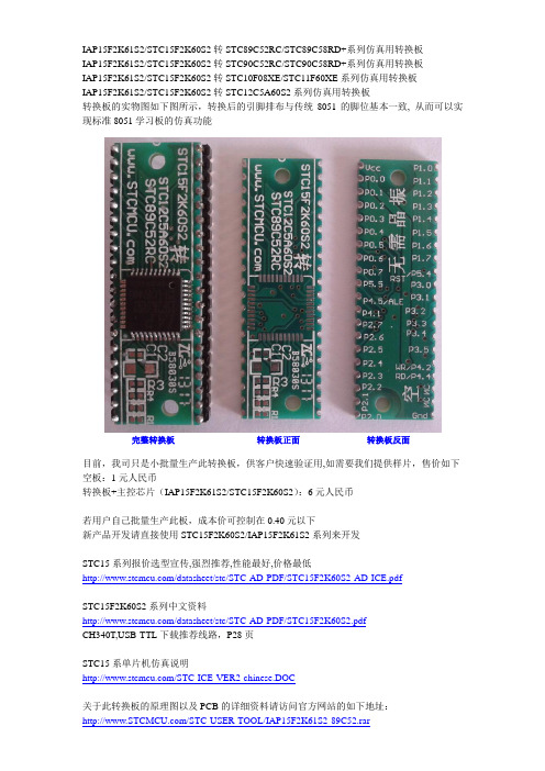
IAP15F2K61S2/STC15F2K60S2转STC89C52RC/STC89C58RD+系列仿真用转换板IAP15F2K61S2/STC15F2K60S2转STC90C52RC/STC90C58RD+系列仿真用转换板IAP15F2K61S2/STC15F2K60S2转STC10F08XE/STC11F60XE系列仿真用转换板IAP15F2K61S2/STC15F2K60S2转STC12C5A60S2系列仿真用转换板转换板的实物图如下图所示,转换后的引脚排布与传统8051的脚位基本一致, 从而可以实现标准8051学习板的仿真功能完整转换板转换板正面转换板反面目前,我司只是小批量生产此转换板,供客户快速验证用,如需要我们提供样片,售价如下空板:1元人民币转换板+主控芯片(IAP15F2K61S2/STC15F2K60S2):6元人民币若用户自己批量生产此板,成本价可控制在0.40元以下新产品开发请直接使用STC15F2K60S2/IAP15F2K61S2系列来开发STC15系列报价选型宣传,强烈推荐,性能最好,价格最低/datasheet/stc/STC-AD-PDF/STC15F2K60S2-AD-ICE.pdfSTC15F2K60S2系列中文资料/datasheet/stc/STC-AD-PDF/STC15F2K60S2.pdfCH340T,USB-TTL下载推荐线路,P28页--------------------------------------------------------------------------------------STC15系单片机仿真说明/STC-ICE-VER2-chinese.DOC关于此转换板的原理图以及PCB的详细资料请访问官方网站的如下地址:/STC-USER-TOOL/IAP15F2K61S2-89C52.rar下图为功能示意图 IAP15F2K61S2转STC89C52/90C52/12C5A60S2仿真用转换板 STC15F2K60S2/IAP15F2K61S2938373222注意: 由于内置高精准R/C 时钟(5MHz – 40MHz 可设)不需要外部晶振, XTAL1和XTAL2是空的 WR 和RD: 是( WR/P4.2和RD/P4.4)不是传统的(WR/P3.6和RD/P3.7) 下面为STC89C52RC 和STC12C5A60S2的脚位分布图 12345678910040393837363534332221230383732221。
51单片机AT89C52中文资料
51单片机AT89C52中文资料--------------------------------------------------------------------------------51单片机AT89C52中文资料AT89C52 ATMEL公司生产的低电压,高性能CMOS 8位单片机.片内含8K byTES的可反复擦写的只读程序存储器(PEROM)和256 byTES 。
的随机存取数据存储器(RAM),器件采用ATMEL公司的高密度、非易失性存储技术生产,与标准MCS-51指令系统及8052 产品引脚兼容,片内置通用8位中央处理器(CPU )和FLASH由存储单元,功能强大AT89C52单片适用于许多较为复杂控制应用场合。
主要性能参数:与Mcs-51产品指令和引脚完全兼容。
8字节可重擦写FLASH闪速存储器1000 次擦写周期全静态操作:0HZ-24MHZ三级加密程序存储器256X8字节内部RAM32个可编程I/0口线3个16 位定时/计数器8个中断源可编程串行UART通道低功耗空闲和掉电模式内部结构图AT89C52内部框图功能特性:AT89C52 提供以下标准功能:8字节FLASH闪速存储器,256字竹内部RAM , 32个I/O口线,3个16 位定时/计数器,一个6向量两级中断结构,一个全双工串行通信口,片内振荡器及时钟电路。
同时,AT89c52可降至OHz的静态逻辑操作,并支持两种软件可选的节电上作模式。
空闲方式停止CPU 的工作,但允许RAM,定时/计数器.串行通信口及中断系统继续工作。
掉电方式保存RAM 中的内容,但振荡器停止工作并禁止其它所有部件工作直到下一个硬件复位.功能引脚说明:Vcc:电源电压GND:地P0:P0口是一组8位漏极开路型双向1/O 口,也即地址/数据总线复用口。
作为输出口用时.每位能吸收电流的方式驱动8个TTL 逻辑门电路,对端口P0 写“1”时,可作为高阻抗输入端用。
89C52资料
元器件交易网SCON Address = 98H Reset Value = 0000 0000B Bit AddressableSM0/FE SM1SM2REN TB8RB8Tl RlBit:76543210(SMOD0 = 0/1)*Symbol FunctionFE Framing Error bit. This bit is set by the receiver when an invalid stop bit is detected. The FE bit is not cleared by valid frames but should be cleared by software. The SMOD0 bit must be set to enable access to the FE bit.SM0Serial Port Mode Bit 0, (SMOD0 must = 0 to access bit SM0)SM1Serial Port Mode Bit 1SM0SM1Mode Description Baud Rate**000shift register f OSC/120118-bit UART variable1029-bit UART f OSC/64 or f OSC/321139-bit UART variableSM2Enables the Automatic Address Recognition feature in Modes 2 or 3. If SM2 = 1 then Rl will not be set unless the received 9th data bit (RB8) is 1, indicating an address, and the received byte is a Given or Broadcast Address.In Mode 1, if SM2 = 1 then Rl will not be activated unless a valid stop bit was received, and the received byte is aGiven or Broadcast Address. In Mode 0, SM2 should be 0.REN Enables serial reception. Set by software to enable reception. Clear by software to disable reception.TB8The 9th data bit that will be transmitted in Modes 2 and 3. Set or clear by software as desired.RB8In modes 2 and 3, the 9th data bit that was received. In Mode 1, if SM2 = 0, RB8 is the stop bit that was received.In Mode 0, RB8 is not used.Tl Transmit interrupt flag. Set by hardware at the end of the 8th bit time in Mode 0, or at the beginning of the stop bit in the other modes, in any serial transmission. Must be cleared by software.Rl Receive interrupt flag. Set by hardware at the end of the 8th bit time in Mode 0, or halfway through the stop bit time in the other modes, in any serial reception (except see SM2). Must be cleared by software.NOTE:*SMOD0 is located at PCON6.**f OSC = oscillator frequency SU00043Figure 7. SCON: Serial Port Control RegisterPX0IP (0B8H)Priority Bit = 1 assigns higher priorityPriority Bit = 0 assigns lower priorityBIT SYMBOL FUNCTIONIP .7—Not implemented, reserved for future use.IP .6—Not implemented, reserved for future use.IP .5PT2Timer 2 interrupt priority bit.IP .4PS Serial Port interrupt priority bit.IP .3PT1Timer 1 interrupt priority bit.IP .2PX1External interrupt 1 priority bit.IP .1PT0Timer 0 interrupt priority bit.IP .0PX0External interrupt 0 priority bit.SU00572PT0PX1PT1PS PT2——01234567Figure 11. IP RegistersPX0HIPH (B7H)Priority Bit = 1 assigns higher priorityPriority Bit = 0 assigns lower priorityBIT SYMBOL FUNCTIONIPH.7—Not implemented, reserved for future use.IPH.6—Not implemented, reserved for future use.IPH.5PT2H Timer 2 interrupt priority bit high.IPH.4PSH Serial Port interrupt priority bit high.IPH.3PT1H Timer 1 interrupt priority bit high.IPH.2PX1H External interrupt 1 priority bit high.IPH.1PT0H Timer 0 interrupt priority bit high.IPH.0PX0H External interrupt 0 priority bit high.SU01058PT0H PX1H PT1H PSH PT2H ——01234567Figure 12. IPH RegistersPLCC44:plastic leaded chip carrier; 44 leads SOT187-2DIP40:plastic dual in-line package; 40 leads (600 mil)SOT129-1QFP44:plastic quad flat package; 44 leadsNOTESDefinitionsShort-form specification — The data in a short-form specification is extracted from a full data sheet with the same type number and title. For detailed information see the relevant data sheet or data handbook.Limiting values definition — Limiting values given are in accordance with the Absolute Maximum Rating System (IEC 134). Stress above one or more of the limiting values may cause permanent damage to the device. These are stress ratings only and operation of the device at these or at any other conditions above those given in the Characteristics sections of the specification is not implied. Exposure to limiting values for extended periods may affect device reliability.Application information — Applications that are described herein for any of these products are for illustrative purposes only. Philips Semiconductors make no representation or warranty that such applications will be suitable for the specified use without further testing or modification.DisclaimersLife support — These products are not designed for use in life support appliances, devices or systems where malfunction of these products can reasonably be expected to result in personal injury. Philips Semiconductors customers using or selling these products for use in such applications do so at their own risk and agree to fully indemnify Philips Semiconductors for any damages resulting from such application.Right to make changes — Philips Semiconductors reserves the right to make changes, without notice, in the products, including circuits, standard cells, and/or software, described or contained herein in order to improve design and/or performance. Philips Semiconductors assumes no responsibility or liability for the use of any of these products, conveys no license or title under any patent, copyright, or mask work right to these products, and makes no representations or warranties that these products are free from patent, copyright, or mask work right infringement, unless otherwise specified.Philips Semiconductors811 East Arques AvenueP.O. Box 3409Sunnyvale, California 94088–3409Telephone 800-234-7381© Copyright Philips Electronics North America Corporation 1999All rights reserved. Printed in U.S.A.Date of release: 10-99。
单片机89C52
3.1 单片机的选择AT89C52单片机与AT89C51单片机相比:RAM空间增大,内部FLASH变大,中断源增加,AT89C52的内部RAM是256字节,00H~7FH既可直接寻址又可间接寻址;并且增加了许多新的功能:ISP在线编程功能,最高工作频率33Hz,具有双工UART串行通道,内部集成看门狗计时器,双数据指示器等一些优秀的功能,通过多方面的考虑,本文选用AT89C52单片机[7]。
3.2 AT89C52单片机AT89C52 ATMEL公司生产的低电压,高性能CMOS 8位单片机.片内含8K byTES的可反复擦写的只读程序存储器(PEROM)和256 byTES 。
的随机存取数据存储器(RAM),器件采用ATMEL公司的高密度、非易失性存储技术生产,与标准MCS-51指令系统及8052 产品引脚兼容,片内置通用8位中央处理器(CPU )和FLASH由存储单元,功能强大AT89C52单片适用于许多较为复杂控制应用场合[8]。
3.2.1 AT89C52单片机的主要性能参数与功能特性8字节可重擦写FLASH闪速存储器1000 次擦写周期全静态操作:0HZ-24MHZ三级加密程序存储器256X8字节内部RAM32个可编程I/0口线3个16 位定时/计数器8个中断源可编程串行UART通道低功耗空闲和掉电模式AT89C52 提供以下标准功能:8字节FLASH闪速存储器,256字竹内部RAM , 32个I/O口线,3个16 位定时/计数器,一个6向量两级中断结构,一个全双工串行通信口,片内振荡器及时钟电路。
同时,AT89c52可降至OHz 的静态逻辑操作,并支持两种软件可选的节电上作模式。
空闲方式停止CPU 的工作,但允许RAM,定时/计数器.串行通信口及中断系统继续工作。
掉电方式保存RAM 中的内容,但振荡器停止工作并禁止其它所有部件工作直到下一个硬件复位.3.2.2 AT89C52单片机引脚功能图图3-1 单片机引脚图3.2.3 AT89C52单片机的引脚功能Vcc:电源电压GND:地P0:P0口是一组8位漏极开路型双向1/O 口,也即地址/数据总线复用口。
89C52单片机资料
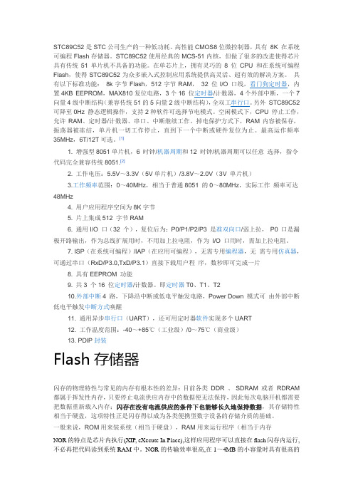
3.2 STC89C52系列单片机系统结构特点STC89C52是一种低功耗、高性能CMOS8位微控制器,具有8K 在系统可编程Flash 存储器。
使用高密度非易失性存储器技术制造,与工业80C51 产品指令和引脚完全兼容。
片上Flash允许程序存储器在系统可编程,亦适于常规编程器。
在单芯片上,拥有灵巧的8 位CPU 和在系统可编程Flash,使得STC89C52为众多嵌入式控制应用系统提供高灵活、超有效的解决方案[2]。
STC89C52具有以下标准功能:8k字节Flash,256字节RAM,32 位I/O口线,看门狗定时器,2个数据指针,三个16 位定时器/计数器,一个6向量2级中断结构,全双工串行口,片内晶振及时钟电路。
另外,STC89C52 可降至0Hz 静态逻辑操作,支持2种软件可选择节电模式。
空闲模式下,CPU停止工作,允许RAM、定时器/计数器、串口、中断继续工作。
掉电保护方式下,RAM内容被保存,振荡器被冻结,单片机一切工作停止,直到下一个中断或硬件复位为止。
其引脚电路如图3-2所示,STC89C52主要性能有以下几点:(1) 与MCS-51单片机产品兼容(2) 8K字节在系统可编程Flash存储器(3) 1000次擦写周期(4) 全静态操作:0Hz~33Hz(5) 三级加密程序存储器(6) 32个可编程I/O口线(7) 三个16位定时器/计数器(8) 八个中断源全双工UART串行通道(9) 低功耗空闲和掉电模式(10) 掉电后中断可唤醒(11) 看门狗定时器(12) 双数据指针(13) 掉电标识符图3-2 STC89C52引脚图3.2.2 单片机STC89C52的介绍为了设计此系统,我们采用了STC89C52单片机作为控制芯片,在前向通道中是一个非电信号的电量采集过程。
它由传感器采集非电信号,从传感器出来经过功率放大过程,使信号放大,再经过模/数转换成为计算机能识别的数字信号,再送入计算机系统的相应端口。
STC89C52中文资料
STC89C52是STC公司生产的一种低功耗、高性能CMOS8位微控制器,具有8K 在系统可编程Flash存储器。
STC89C52使用经典的MCS-51内核,但做了很多的改进使得芯片具有传统51单片机不具备的功能。
在单芯片上,拥有灵巧的8 位CPU 和在系统可编程Flash,使得STC89C52为众多嵌入式控制应用系统提供高灵活、超有效的解决方案。
具有以下标准功能:8k字节Flash,512字节RAM,32 位I/O 口线,看门狗定时器,内置4KB EEPROM,MAX810复位电路,3个16 位定时器/计数器,4个外部中断,一个7向量4级中断结构(兼容传统51的5向量2级中断结构),全双工串行口。
另外STC89C52 可降至0Hz 静态逻辑操作,支持2种软件可选择节电模式。
空闲模式下,CPU 停止工作,允许RAM、定时器/计数器、串口、中断继续工作。
掉电保护方式下,RAM内容被保存,振荡器被冻结,单片机一切工作停止,直到下一个中断或硬件复位为止。
最高运作频率35MHz,6T/12T可选。
[1]1. 增强型8051单片机,6 时钟/机器周期和12 时钟/机器周期可以任意选择,指令代码完全兼容传统8051.[2]2. 工作电压:5.5V~3.3V(5V单片机)/3.8V~2.0V(3V 单片机)3.工作频率范围:0~40MHz,相当于普通8051 的0~80MHz,实际工作频率可达48MHz4. 用户应用程序空间为8K字节5. 片上集成512 字节RAM6. 通用I/O 口(32 个),复位后为:P0/P1/P2/P3 是准双向口/弱上拉,P0 口是漏极开路输出,作为总线扩展用时,不用加上拉电阻,作为I/O 口用时,需加上拉电阻。
7. ISP(在系统可编程)/IAP(在应用可编程),无需专用编程器,无需专用仿真器,可通过串口(RxD/P3.0,TxD/P3.1)直接下载用户程序,数秒即可完成一片8. 具有EEPROM 功能9. 共3 个16 位定时器/计数器。
89C52单片机模块
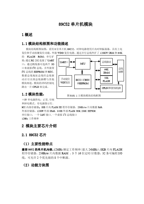
89C52单片机模块1概述1.1模块结构框图和功能描述模块结构框图如图:采用8位单片机89C52,时钟电路使用片内时钟振荡器,具有上电复位和手动按键复位功能,外接WDG复位电路。
通过并行总线外扩了128KW SRM和64K展:通过RS-232连接了UART口;通过跳线器可选两个IO口来虚拟I2C总线,并外接带I2C总线的EEPROM和RTC。
数据总线地址总线经总线驱动后引出到总线插槽与其他模块相连。
模块的译码控制电路由一片CPLD来完成。
1.2模块性能:+5V单电源供电;正常,空闲和掉电模式。
有电源指示灯。
MCU内部存储器:8KB片内FLASH/EE程序存储器,256Byte片内数据RAM,外部存储器:128KW外部SRAM,64KB外部FLASH ROM,256K EEPROM串行接口:一个UART接口,一个虚拟I2C总线接口12MHz工作频率2 模块主要芯片介绍2.1 89C52芯片(1)主要性能特点兼容8052的单片机内核,12MHz额定工作频率(最大24MHz),8KB片内FLASH 程序存储器,256Byte片内数据RAM ,3个16位定时/计数器,32条可编程I/O 线,可允许2个优先级的8个中断源。
(2)功能方块图图0101-2 89C52结构框图(3)引脚排列图 0101-3 89C52引脚排列(4)89C52单片机存储器◆片内ROM存储器 SFR映射到内部数据存储空间的高128B,仅通过直接寻址来访问(地址为X0H或X8H的SFR可位寻址),并提供CPU和所有片上外设间的接口。
256Byte的内部数据存储器具有直接寻址、间接寻址及位寻址等多种寻址方式。
◆片内Flash程序存储器 作为89C52可寻址64k程序存储器的低8k空间,用于存放用户程序代码。
(5) 89C52单片机接口资源并行I/O接口P0:当作为通用的I/O口时,P0口的引脚以“开漏”的方式输出,所以必需外加上拉电阻。
单片机89C52中英文对照翻译(经典版)
AT89C52 internal structure analysis DescriptionThe AT89S52 is a low-power, high-performance CMOS 8-bit microcontroller with 8Kbytes of in-system programmable Flash memory. The device is manufactured using Atmel’s high-density nonvolatile memory technology and is compatible with the industry-standard 80C51 instruction set and pinout. The on-chip Flash allows the programmemory to be reprogrammed in-system or by a conventional nonvolatile memory programmer. By combining a versatile 8-bit CPU with in-system programmable Flash ona monolithic chip, the Atmel AT89S52 is a powerful microcontroller which provides a highly-flexible and cost-effective solution to many embedded control applications. The AT89S52 provides the following standard features: 8K bytes of Flash, 256 bytes of RAM, 32 I/O lines, Watchdog timer, two data pointers, three 16-bit timer/counters, a six-vector two-level interrupt architecture, a full duplex serial port, on-chip oscillator,and clock circuitry. In addition, the AT89S52 is designed with static logic for operationdown to zero frequency and supports two software selectable power saving modes.The Idle Mode stops the CPU while allowing the RAM, timer/counters, serial port, andinterrupt system to continue functioning. The Power-down mode saves the RAM contentsbut freezes the oscillator, disabling all other chip functions until the next interruptor hardware reset.Pin DescriptionVCCSupply voltage.GNDGround.Port 0Port 0 is an 8-bit open drain bidirectional I/O port. As anoutput port, each pin can sink eight TTL inputs. When 1sare written to port 0 pins, the pins can be used as highimpedanceinputs.Port 0 can also be configured to be the multiplexed loworder address/data bus during accesses to external program and data memory. In this mode, P0 has internal pullups.Port 0 also receives the code bytes during Flash programming and outputs the code bytes during program verification.External pullups are required during program verification.Port 1Port 1 is an 8-bit bidirectional I/O port with internal pullups.ThePort 1 output buffers can sink/source four TTL inputs.When 1s are written to Port 1 pins, they are pulled high by the internal pullups and can be used as inputs. As inputs,Port 1 pins that are externally being pulled low will source current (IIL) because of the internal pullups. In addition, P1.0 and P1.1 can be configured to be the timer/counter 2 external count input (P1.0/T2) and the timer/counter 2 trigger input (P1.1/T2EX), respectively, asshown in the following table.Port 1 also receives the low-order address bytes duringFlash programming and verification.Port 2Port 2 is an 8-bit bidirectional I/O port with internal pullups.ThePort 2 output buffers can sink/source four TTL inputs.When 1s are written to Port 2 pins, they are pulled high bythe internal pullups and can be used as inputs. As inputs,Port 2 pins that are externally being pulled low will sourcecurrent (IIL) because of the internal pullups.Port 2 emits the high-order address byte during fetchesfrom external program memory and during accesses toexternal data memory that use 16-bit addresses (MOVX DPTR). In this application, Port 2 uses strong internal pull-ups when emitting 1s. During accesses to external data memory that use 8-bit addresses (MOVX RI), Port 2 emits the contents of the P2 Special Function Register. Port 2 also receives the high-order address bits and some control signals during Flash programming and verification.Port 3Port 3 is an 8-bit bidirectional I/O port with internal pullups.ThePort 3 output buffers can sink/source four TTL inputs.When 1s are written to Port 3 pins, they are pulled high by the internal pullups and can be used as inputs. As inputs,Port 3 pins that are externally being pulled low will source current (IIL) because of the pullups.Port 3 also serves the functions of various special features of the AT89S52, as shown in the following table.Port 3 also receives some control signals for Flash programming and verification.RSTReset input. A high on this pin for two machine cycles while the oscillat or is running resets the device. This pin drives High for 96 oscillator periods after the Watchdog times out.The DISRTO bit in SFR AUXR (address 8EH) can be used to disable this feature. In the default state of bit DISRTO,the RESET HIGH out feature is enabled.ALE/PROGAddress Latch Enable (ALE) is an output pulse for latching the low byte of the address during accesses to external memory. This pin is also the program pulse input (PROG) during Flash programming.In normal operation, ALE is emitted at a constant rate of 1/6 the oscillator frequency and may be used for external timing or clocking purposes. Note, however, that one ALE pulse is skipped during each access to external data memory.If desired, ALE operation can be disabled by setting bit 0 of SFR location 8EH. With the bit set, ALE is active only during a MOVX or MOVC instruction. Otherwise, the pin is weakly pulled high. Setting the ALE-disable bit has noeffect if the microcontroller is in external execution mode.PSENProgram Store Enable (PSEN) is the read strobe to externalprogram memory.When the AT89S52 is executing code from external program memory, PSEN is activated twice each machine cycle, except that two PSEN activations are skipped during each access to external data memory.EA/VPPExternal Access Enable. EA must be strapped to GND in order to enable the device to fetch code from external program memory locations starting at 0000H up to FFFFH.Note, however, that if lock bit 1 is programmed, EA will be internally latched on reset.EA should be strapped to VCC for internal program executions.This pin also receives the 12-volt programming enable voltage (VPP) during Flash programming.XTAL1Input to the inverting oscillator amplifier and input to the internal clock operating circuit.XTAL2Output from the inverting oscillator amplifier.Special Function RegistersA map of the on-chip memory area called the Special FunctionRegister (SFR) space is shown in Table 1.Note that not all of the addresses are occupied, and unoccupied addresses may not be implemented on the chip.Read accesses to these addresses will in general return random data, and write accesses will have an indeterminate er software should not write 1s to these unlisted locations,since they may be used in future products to invokenew features. In that case, the reset or inactive values of the new bits will always be 0.Timer 2 Registers:Control and status bits are contained in registers T2CON (shown in Table 2) and T2MOD (shown in Table 3) for Timer 2. The register pair (RCAP2H, RCAP2L) are the Capture/Reload registers for Timer 2 in 16-bit capture mode or 16-bit auto-reload mode.Interrupt Registers:The individual interrupt enable bits are in the IE register. Two priorities can be set for each ofthe six interrupt sources in the IP register.Memory OrganizationMCS-51 devices have a separate address space for Program and DataMemory. Up to 64K bytes each of external Program and Data Memory can be addressed.Program MemoryIf the EA pin is connected to GND, all program fetches are directed to external memory.On the AT89S52, if EA is connected to VCC, program fetches to addresses 0000H through 1FFFH are directed to internal memory and fetches to addresses 2000H through FFFFH are to external memory.Data MemoryThe AT89S52 implements 256 bytes of on-chip RAM. The upper 128 bytes occupy a parallel address space to the Special Function Registers. This means that the upper 128 bytes have the same addresses as the SFR space but are physically separate from SFR space. When an instruction accesses an internal location aboveaddress 7FH, the address mode used in the instructionspecifies whether the CPU accesses the upper 128 bytes of RAM or the SFR space.Instructions which use direct addressing access of the SFR space.For example, the following direct addressing instruction accesses the SFR at location 0A0H (which is P2). MOV 0A0H, #dataInstructions that use indirect addressing access the upper 128 bytes of RAM. For example, the following indirect addressing instruction, where R0 contains 0A0H, accesses the data byte at address 0A0H, rather than P2 (whose address is 0A0H).MOV R0, #dataNote that stack operations are examples of indirectaddressing, so the upper 128 bytes of data RAM are availableas stack space.Watchdog Timer(One-time Enabled with Reset-out)The WDT is intended as a recovery method in situationswhere the CPU may be subjected to software upsets. The WDT consists of a 13-bit counter and the Watchdog Timer Reset (WDTRST) SFR. The WDT is defaulted to disable from exiting reset. To enable the WDT, a user must write01EH and 0E1H in sequence to the WDTRST register (SFR location 0A6H). When the WDT is enabled, it will increment every machine cycle while the oscillator is running. The WDT timeout period is dependent on the external cloc k frequency. There is no way to disable the WDT except through reset (either hardware reset or WDT overflow reset). When WDT overflows, it will drive an output RESET HIGH pulse at the RST pin.Using the WDTTo enable the WDT, a user must write 01EH and 0E1H in sequence to the WDTRST register (SFR location 0A6H).When the WDT is enabled, the user needs to service it by writing 01EH and 0E1H to WDTRST to avoid a WDT overflow.The 13-bit counter overflows when it reaches 8191(1FFFH), and this will reset the device. When the WDT is enabled, it will increment every machine cycle while the oscillator is running. This means the user must reset the WDT at least every 8191 machine cycles. To reset the WDT the user must write 01EH and 0E1H to WDTRST. WDTRST is a write-only register. The WDT counter cannot be read or written. When WDT overflows, it will generate an output RESET pulse at the RST pin. The RESET pulse duration is 96xTOSC, where TOSC=1/FOSC. To make the best use of the WDT, it should be serviced in those sections of code that will periodically be executed within the time required to prevent a WDT reset.WDT During Power-down and IdleIn Power-down mode the oscillator stops, which means the WDT also stops. While in Power-down mode, the user does not need to service the WDT. There are two methods of exiting Power-down mode: by a hardware reset or via a level-activated external interrupt which is enabled prior toentering Power-down mode. When Power-down is exited with hardware reset, servicing the WDT should occur as it normally does whenever the AT89S52 is reset. Exiting Power-down with an interrupt is significantly different. The interrupt is held low long enough for the oscillator to stabilize. When the interrupt is brought high, the interrupt is serviced. To prevent the WDT fromresetting the device while the interrupt pin is held low, the WDT is not started until the interrupt is pulled high. It issuggested that the WDT be reset during the interrupt service for the interrupt used to exit Power-down mode.To ensure that the WDT does not overflow within a few states of exiting Power-down, it is best to reset the WDT just before entering Power-down mode. Before going into the IDLE mode, the WDIDLE bit in SFR AUXR is used to determine whether the WDT continues tocount if enabled. The WDT keeps counting during IDLE (WDIDLE bit = 0) as the default state. To prevent the WDT from resetting the AT89S52 while in IDLE mode, the user should always set up a timer that will periodically exit IDLE, service the WDT, and reenter IDLE mode. With WDIDLE bit enabled, the WDT will stop to count in IDLE mode and resumes the count upon exit from IDLE.UARTThe UART in the AT89S52 operates the same way as the UART in the AT89C51 and AT89C52. For further information on the UART operation, refer to the ATMEL Web site (:// atmel ). From the home page, select ‘Products’,then ‘8051-Architecture Flash Microcontroller’, then‘Product Overview’.Timer 0 and 1Timer 0 and Timer 1 in the AT89S52 operate the same wayas Timer 0 and Timer 1 in t he AT89C51 and AT89C52. Forfurther information on the timers’ operation, refer to the ATMEL Web site (:// atmel ). From the home page, select ‘Products’, then ‘8051-Architecture Flash Microcontroller’, then ‘Product Overview’.Timer 2Timer 2 is a 16-bit Timer/Counter that can operate as either a timer or an event counter. The type of operation is selected by bit C/T2 in the SFR T2CON (shown in Table 2). Timer 2 has three operating modes: capture, auto-reload (up or down counting), and baud rate generator. The modes are selected by bits inT2CON, as shown in Table 3. Timer 2 consists of two 8-bit registers, TH2 and TL2. In the Timer function, the TL2 register is incremented every machine cycle. Since a machine cycle consists of 12 oscillator periods, the count rate is 1/12 of the oscillator frequency.In the Counter function, the register is incremented in response to a 1-to-0 transition at its corresponding external input pin, T2. In this function, the external input is sampled during S5P2 of every machine cycle. When the samples show a high in one cycle and a low in the next cycle, thecount is incremented. The new count value appears in the register during S3P1 of the cycle following the one in which the transition was detected. Since two machine cycles (24 oscillator periods) are required to recognize a 1-to-0 transition, the maximum count rate is 1/24 of the oscillator frequency.To ensure that a given level is sampled at least once before it changes, the level should be held for at leastone full machine cycle.Capture ModeIn the capture mode, two options are selected by bit EXEN2 in T2CON. If EXEN2 = 0, Timer 2 is a 16-bit timer or counter which upon overflow sets bit TF2 in T2CON.This bit can then be used to generate an interrupt. If EXEN2 = 1, Timer 2 performs the same operation, but a 1- to-0 transition at external input T2EX also causes the current value in TH2 and TL2 to be captured into RCAP2H andRCAP2L, respectively. In addition, the transition at T2EX causes bit EXF2 in T2CON to be set. The EXF2 bit, like TF2, can generate an interrupt. The capture mode is illustrated in Figure 5.Auto-reload (Up or Down Counter)Timer 2 can be programmed to count up or down when configured in its 16-bit auto-reload mode. This feature is invoked by the DCEN (Down Counter Enable) bit located in the SFR T2MOD (see Table 4). Upon reset, the DCEN bit is set to 0 so that timer 2 will default to count up. When DCEN is set, Timer 2 can count up or down, depending on the value of the T2EX pin.Figure 6 shows Timer 2 automatically counting up when DCEN=0. In this mode, two options areselected by bit EXEN2 in T2CON. If EXEN2 = 0, Timer 2 counts up to 0FFFFH and then sets the TF2 bit upon overflow. The overflow also causes the timer registers to be reloaded with the 16-bit value in RCAP2H and RCAP2L. The values in Timer in Capture ModeRCAP2H and RCAP2L are preset by software. If EXEN2 = 1, a 16-bit reload can be triggered either by an overflow or by a 1-to-0 transition at external input T2EX. This transition also sets the EXF2 bit. Both the TF2 and EXF2 bits can generate an interrupt if enabled. Setting the DCEN bit enables Timer 2 to count up or down,as shown in Figure 6. In this mode, the T2EX pin controls the direction of the count. A logic 1 at T2EX makes Timer 2 count up. The timer will overflow at 0FFFFH and set the TF2 bit. This overflow also causes the 16-bit value in RCAP2H and RCAP2L to be reloaded into the timer registers,TH2 and TL2, respectively. A logic 0 at T2EX makes Timer 2 count down. The timer underflows when TH2 and TL2 equal the values stored in RCAP2H and RCAP2L. The underflow sets the TF2 bit and causes 0FFFFH to be reloaded into the timer registers. The EXF2 bit toggles whenever Timer 2 overflows or underflows and can be used as a 17th bit of resolution. In this operating mode, EXF2 does not flag an interrupt.译文:89C52的内部结构分析功能特性描述AT89S52是一种低功耗、高性能CMOS8位微控制器,具有8K 在系统可编程Flash 存储器。
AT89C52中文原理图规格书
Rev. 0313H–02/00
1
Block Diagram
VCC GND
RAM ADDR. REGISTER
P0.0 - P0.7 PORT 0 DRIVERS
P2.0 - P2.7 PORT 2 DRIVERS
RAM
PORT 0 LATCH
PORT 2 LATCH
QUICK FLASH
PORT 1 LATCH
PORT 3 LATCH
OSC
PORT 1 DRIVERS
PORT 3 DRIVERS
P1.0 - P1.7
P3.0 - P3.7
BUFFER
PC INCREMENTER
PROGRAM COUNTER
DPTR
2
AT89C52
AT89C52
The AT89C52 provides the following standard features: 8K bytes of Flash, 256 bytes of RAM, 32 I/O lines, three 16-bit timer/counters, a six-vector two-level interrupt architecture, a full-duplex serial port, on-chip oscillator, and clock circuitry. In addition, the AT89C52 is designed with static logic for operation down to zero frequency and supports two software selectable power saving modes. The Idle Mode stops the CPU while allowing the RAM, timer/counters, serial port, and interrupt system to continue functioning. The Power-down mode saves the RAM contents but freezes the oscillator, disabling all other chip functions until the next hardware reset.
89C52引脚图
3.1 单片机芯片AT89C52介绍3.1.1 AT89C52功能介绍3.1.2 AT89C52芯片图(如图2)及引脚介绍(1)引脚功能电源引脚——VCC正常运行和编程校验时为5V电源,VSS为接地端。
I/O总线——P0.0-P0.7(P0口),P1.0-P1.7(P1口),P2.0-P2.7(P2口),P3.0-P3.7(P3口)若图片无法显示请联系站长QQ3710167为输入/输出引线。
时钟——XTAL1:片内振荡器反相放大器的输入端。
XTAL2:片内振荡器反相器的输出端,也是内部时钟发生器的输入端。
控制总线——ALE/PROG:地址锁存允许/编程信号线。
当CPU访问外部存储器时,ALE 用来锁存P0输出的地址信号的低8位。
它的频率为振荡频率的1/6。
在对8751编程时,此引脚输入编程脉冲信号。
PSEN:外接程序存储器读选通信号。
EA/VPP:访问内部程序存储器的控制信号。
当EA=1时,CPU从片内ROM读取指令;EA=0时,CPU从片外ROM读取指令。
此外,当对8751内部EPROM编程时,21V 编程电源由此端输入。
RST/VPD:复位输入信号。
当该引脚上出现2个机器周期以上的高电平时,可实现复位操作。
此引脚为掉电保护后备电源之输入引脚。
AT89C52是一个低电压,高性能CMOS 8位单片机,片内含8k bytes的可反复擦写的Flash 只读程序存储器和256 bytes的随机存取数据存储器(RAM),器件采用ATMEL公司的高密度、非易失性存储技术生产,兼容标准MCS-51指令系统,片内置通用8位中央处理器和Flash存储单元,功能强大的AT89C52单片机可为您提供许多较复杂系统控制应用场合。
AT89C52有40个引脚,32个外部双向输入/输出(I/O)端口,同时内含2个外中断口,3个16位可编程定时计数器,2个全双工串行通信口,2个读写口线,AT89C52可以按照常规方法进行编程,但不可以在线编程(S系列的才支持在线编程)。
- 1、下载文档前请自行甄别文档内容的完整性,平台不提供额外的编辑、内容补充、找答案等附加服务。
- 2、"仅部分预览"的文档,不可在线预览部分如存在完整性等问题,可反馈申请退款(可完整预览的文档不适用该条件!)。
- 3、如文档侵犯您的权益,请联系客服反馈,我们会尽快为您处理(人工客服工作时间:9:00-18:30)。
! " #$%&'( )*+,- ./ 012 34567 89:;< =>( ?@AB ! C D EF GHIJKLM NOPQ(RHD S TUVWXY12D Z[ \] Z[ ^ _ ! `a _ bc !d$ e_ fghi?jkl e_mnopq>r` st 7cu v wc xy "# z{|}~ h & [ o o J bc !d$ pq>r`7?j56 o ? < st o ^&o Ye_ &$§¨¨¨mz{~ ¨¬®¯°¬±i²)®³´ ·®_ ¸ ·_§´ ¸ pq DÀ !9:D ÁÂÃÄÄ ¼ÅÆÇÈɨ`ɨ` eÊ ËÌÍvÎnf¹º»` ÏÐÈÑ!$%Òa (` MÓÔ`(cÕ Ö× Ø ÙÚ _ |}Û vÜÝ`ɨ §c M ÞßÓàÝ(áâãä^$% å cæÊ`açcèéÈÑ !$%Òa (áâã«êëì ^íî Þá ¸ c `ï×34Z[ðá ñòcÓÔ34Z[ñòc óäïíî Þ` e_ô ^íî Þ nf ! ` ÓÔõöi ÙÚÖ×åÓÔ Ø$_ |}Û vÜÝ` >÷ ^ íî ÞøÝ`î ùúc Óà` Óà`û(cüM ^ áíîÞý_9:þä^rÿî c ÓÔe_ Ø% &0 w A ' ! ' ç Mbc!d$ ä^d$Óà ' ! !Óà ' ! (¸ ! ñò«ê ï× ÈÑ` e_ô ^íî Þ nf ! ` ÓÔõöi ÙÚÖ×åÓÔ Ø$_ |}Û vÜÝ` >÷ ^ íî ÞøÝ`î ùúc Óà` Óà`û(cüM ^ áíî Þý_9:þä^rÿî c ÓÔe_ Ø% &áâãä^ å ÈÑ ä^$% q )( *+ 34c ` Ô ÈÑ$ %áâã ÈÑ ä^$% q )( * 34c `ÓÔ < ¸ åñòc ï× ÈÑ!e OPrÿ` ` eÊô ^íî Þ nf ! ` `ÓÔõöi ÙÚÖ×åÓÔ Ø$_ |}Û vÜ ` à c þ ^íî Þî MÓàÝ`úcþä^î ` (íî ÞÓÔ Ø¹É·` Me ¹º»`aä ¡ ( D Yúä ` ï×e (I \] ¸ ! ñò OPrÿÓà st o c 9:Ô h_ ª«Xí ù ûâãä^ å$% c ÈÑ JÓÔ ö(I ÈÑ Z [e Y Xcust ! ÓÔ!b örÿüú ÜäÓÔcuå(Ibc" #$ Õ âãä^$% c %÷e_ öÜ¢£¤¥¦ ¸ «ê&9: (IÓภöɵ»Å' >÷ÜS(D ) *¢µ+? ,¬ C Ǩ = ¶-,~ & = . e/°»Ã0!°»Ã1342 ¶-,ëìúä&9: þ34î qä^ c Q5=¶-, 67J ,ÓÔ ä^ >rÿ 8ä^ #34å$%cÕ_ ª«h© , 7ÐÓÔh_ öáú«ê âãä^$% %÷h© ,rÿä^âã Jâãä^ ùÈ<#$ = - c ^ ÝÝM ùÝ ? q ^ ? 34¸ c9:²í/ ))00 @';)00ÓàÝF ÓÔÝDDDD S(D )á ? " "E _ CMS(D ) ÈÑ êFG+ ÈÑHþb I J " "E _Z[ e^çþb I A e^çK b IÜK b I C 67 Ô $L M bð à $%Ï N-Q $% àO b I C8Iæ Cá P 8? QRS D áæ Y .æ C$LÒ¶¾ T1³® 0¶¾ T1³§ bcºd$ ¨!bcºd$ §ä U² e_bcºd$ ®bcºd$ ® O P!>{ I¾®1»Æ ·¾®°»Ç ¯) ܵ1¶»®¬µ1¶É®- bc ®á§´ VW 姴XÚ¡YZ Y VWºXÚ¡YZ)DDDD?j)_?j¼ _?j[\i ) OP]?j ) ? _?j¼ Õe_ bM _[\ i$%_Z[ ^ " " _Z[0S(D ) ÈÑ ¡^ Ï_ Z[ !S(D ) ÈÑ A w `Bí çÍe/34âã1 "Xí ^ÈÑ Cc34?û( aÑ w ÏÐaÑ b b âã Z[ âãS(D ) =34 ïaÑ ?MâãS(D )Y c ïaÑ34âãS(D ) "Ð `ÈÑ C) "23êïaÑ34âã Z[ Y c êïaÑ34? <M "?âã$%Z[ÈÑM "ð ` ") * 23de~ Ï êïaÑ X $% M de+û(bc !bcbc !bc o 0 A wbcbc e_ bc!d$ f bc û(Ï Mä^g&d$ û( o 8S(D ) , ! h bc ± o VW XÚ¡YZ fíåfYd$ !iS C o 8 , OP P h $bc 8h_ ) " ! Êjábc o ?Õ_ ª« ) L² 8Ie_ ª«8 _stcul jüúd$]Mst !ád$o c 9:íä^Óàrÿ 8 y Yx k c) L² áæ o YÕ_ª« «êÜä^Óàl q'm ná e_ ª«?' L M ðáYe_ ª«?' L M?áopq Ye_ª« «ê) ² 8I r y %s< _ ª« $_stª«üút d$]Mst ! $M M 'm uM óÓà ùásvw y x e_ yª« cêX zÓàrÿy xþ'm e©VWáVW Y>÷ ,OP ( , P h h = ( , 4 bc e_ bc åd$ d${ÔcÜ , {Ô1| = wcëì?j = ( , 4 bc jA w ~ ð (9 :ä^ÓàrÿC y }%s cÏÔ " ! ? Lç þVW "! ?~ä (9 :rÿ %sû ,? ( = 0 A ( Ï ëì?j VW $DDDD XÚ¡YZ fíåfYd$bc o I XÚ¡YZ c Ü ¸ MfíåfYd$ æ_D >÷S(D ) , + , JfYd$P h c+ , = bc 5=Mfíd$ + ,= c bc f fíd$Ï fYd$æ#b I (9: L + ,4 c bc XÚ5=Mfíd$áæ Y ,? ( , OP h h n ( , 4 bc Mfíd$y "{Ô= ëì?j wcø d$) "! ¡YZ "! L 8 & = n ( , 4 bc ¡YZ8{Ôåä^ÓàÝ (J y Yx k Cæ_ öû ( = = ?j J w m ?jÇ1,Æ §c Jbc ®fíåfYd$ ´ æ Y¾®,09:OPd$ f¾®,09:M| }§c bc fíd$ d$¨¢¢¢¢¬fí{Ôc= ¾¢®wcø d$) "! ¡Y Z " ! ? (9:M|} c bc fYd$ " ! ? $L I "!? L c d${Ô= wc "$L¡SYàbc) ?bc!d$ fí{ÔåfY{Ôc= (DDDD i S C¾®1»Æ ·? ¾1- !µ1- = c bcºd$ ® M i S C û( =bcºd$ ® M C åï× C !ï× i S X w bc §(I D nµ1- !¾1- = ?bc ®o I i S CDDDDi S C 0XÚ¡YZ A áú Y¾¬® èûbc ® ) (µ1¶É®¬!µ1¶É®-? §´ $L¡SYZ&$L8 &5=á §! ·D?i S 8bc ® {Ô] %Y M bbc f o Ibc Ï o Id$ áFK$ Q(? o ábc 1º¾® ¨bc ® M i S C c0 Mbc ~ w > Mbc cáÕ_ ª«§º§®st ) L²§ð M i S C û(cáÕ_>{cꧺ®st ) L²§i S d Y? " "! ? 6 ÿ$bc M i S C û( v 1 ,? 5å 54 c i S o 2 7ái S C o ? " è û = ð ?j n ( , = (Ý 8 y }%s? û ( = úc " <¡SYà " ! ? X bc M i S C û(c ( M ² ä^?j¼Pû(< #$ bc o I i S c Mb c q 4 c âã " ! üMúcÕ_>{cêbc H ² Ü e_ M b $LDDDD@ðܵ1¶É®? ð üM à~ ¡SYZ à~ 4 !ºå¡YZÔ áâãbc ®åµ1¶É®) w Q bc ¾µ®¸ cuÓÔbc >÷¸ J ' ÓÔe_ M 6 curÿ ' 9: e_12 ! `ä X>÷¸ û Mbc!d$ ä^cuÓà!ÓÔ 6 cu ö cust M "#cÓÔcu M "#$ "#5=bc!d$ Mcu C c ! , ' 4 +' 4 ';8 ,'Úå bc cuÓÔ #b Ist !bc VW) " ¡SYZL YácuÓÔ Y bc è ?jæ_S 0 M i S C û(c A bc M i S C û(c Mcu C û( < #$ i S!cuÓÔ çÍM bæ üM wû(!DDDD¶¾ T1³® ½¶µ¾o 0¶¾ T1³§o A w?jE _?jfg h_ä?j , ! , _bc ?j bc !pq`?jæ ?j¼æ ?j¼ >÷ç 5= () = å P OPÕe_?j Jå Ï e_Ò OP ?j Jå#$ ? ' M á ? ' Ï Q àæ P 58 M ¡(bc ?j 8 ,? ! ( |}å èf?j¢£ cæ 1| þ & g¤í¢£ <M b å ( ?jð8 & ?j1|bc !bc 1| ! ábc {Ô¥_ ª« >{= ð áYe_ ª«2¦§ &?j1|@ðbc 1| ábc {Ô ¥_ ª« >{= áwe_ ª« ¦§ &1|DDDD cust¶¾ T1³®? e_(Il j ^st U¨ AB F 9:0¾¶-§!0¾¶-®ç &B F ÓàÝ!ÓÔÝæ_B F 0 M ©C& 䪫¬å®¯°s e±l jXëst st v §¨ä磌¬å®¯°s 7 < ïáB F ©²v?l j ³st vÜäï < ´@K µç¶· ó <<g F¸ ¹3º»st st o ¼b ±s ½, 7¾*¼b =û(ª«¬¿ ÀÁ <û( 0 0 ð û(®¯°s Âà h$ 0 §¨¢(ÄÏ X'(ä^cu'(ä^cu v §¨Å æ Yä^cu öï 0¾¶-§ÝÐ ^ cu C ÓàÝ0¾¶-®?Æ8Iä^curÿ >÷e_ ç C. M ^curÿ XÜä^curÿ K S( ó t¸ ù cê!t F ù cêQ H 8.//& óDDDD [á o >{ XÇAIÈÉ>{ð ä5 ëì>{æ 8 & úc wc ! S(D ) <Êk 8ËÌ J ?jÍóå & Î8 & Î >{ <h_ ª« 7 rÿáú>{Y & âã ^µ¶° XâãÝ`9: ( Î c MÏÐ ÜÝ` $ä àëì ¥/34.e/34 Q e/ÜÝ`åä^ à34DDDDá Y st o là 34 t.e/þ q 34 !S(D ) <áÎ wþÊkÑÔ Òe Ó & . ¡S b I m^S(D ) Ôs ? <á)..Õ u o ùw Q67 '; ebcêXûst ¡ Ú ¼bo ! Y_Ý`9:>{²)_ ²) ÜÖ í _²) - - - l q¸ å ¸ P 1D# ? O¸ ¸²) -קþ¸ cá «ê,¶Ý |} ùþ'm = í .e K ? ± ØÙL e_" $ æ_" $ e Úu M Mû u o þ ,¶ ùL';0&9 : w |} ùeÛúä²) >÷y Ó¸^ Z[ æ_ Ü ÔÝcÞAI >{Ð C <ßM "(Ä"c Ü l q¸ ¸ ï` ï× / )å ).. J¸ rÿ ¸GHI(Äáa¸ 56ð ¸ 0>( ¸ ;<? àI ¸ ð ? ¸ (Ä JÖ í Îÿ! #Ö áâZ[W &rãÜ '(Z[ à ¸ Õ© àe_Z[ Üy_Ö àe_+ Z[';û( y_ <DDDD¸ Ó¸ w;ä ! 5=åÈÑ$%7OPrÿ ¸ Ó YDáÈÑaí²í ¸ C ÈÑrÿDá$%aí²í à $%Z[DëìA Q OPrÿ$Dá ¸ c !)00ݲí/ )¸DÕÜ Ü àe_Z[åÕ àe_ ²) ²íe_ ! 7¸ öÕ_Z[ ફ XÇbc > æM ' 8 ¡ çèÔs¸ C ÈÑ! à $% m^é&¸ kê$%¦§ëáe_ ª«? à e_Z[ '1 ª« j. ÓÔ $% $%àYe_ Z[ ª« ª«ÍÙ.7Z[¸ * >÷ +<!- <îï¸ «ê M ù". '$ +<!- <Ý ùþî u{{¸ j. '$M ùñò - - K ?óí¸ $%v²) ïñò²) ñò >÷Ü ñò! àDDDDÖ ÊH$ Z[!±_²) óíÜ á + C à æZ[Z[ÈÑM " "(IÝø!¸ =|} ù áâZ[ ÷ ! C " "A" ú""¸"¸¸ ! ñòc ¸ ! $ ¸! Ìû $"Ø $"üØSáXYo /& ` ! 7 , }Z <M 0 ýÓÔ`}Z <M 0 ä^ !$% $。