中文数据手册AT24C系列
AT24CO4中文资料

编辑本段 AT24C04 特点AT24C04,采用DIP封装方式。
存储器配置:512 x 8bit封装类型:DIP针脚数:8工作温度范围:-40°C to +85°C封装类型:DIP器件标号:24器件标记:24C04存储器容量:4Kbit存储器电压 Vcc:2.5V存储器类型:EEPROM工作温度最低:-40°C工作温度最高:+85°C接口类型:Serial, I2C电压, Vcc:5.5V电源电压最大:5.5V电源电压最小:1.8V芯片标号:24C04表面安装器件:通孔安装逻辑功能号:24C04频率:1MHz1、AT24C04介绍关于I2C的介绍,这里就不用说了,直接介绍24C04了。
24C04是4K位串行CMOS E2PROM。
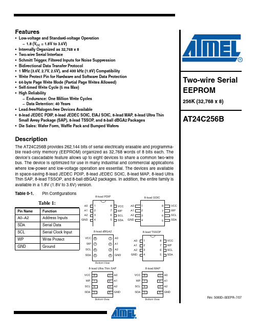
引脚的认识:SCL 串行时钟引脚SDA 串行数据/地址A0、A1、A2 器件地址输入端WP 写保护(WP 管脚连接到Vcc,所有的内容都被写保护(只能读)。
当WP 管脚连接到Vss 或悬空,允许器件进行正常的读/写操作。
)2、AT24C04之准备工作首先,我们先查看一下实验板上面的接线图。
如图1所示。
图1 24c04连接图我们要注意的第一点是器件地址全部是0,即接地处理。
第二点是读写保护WP接地,意味着我们可以随意存取。
第三点是我们要用到的引脚连接到了P3^6和P3^7上。
在这里还要提醒一下,就是引脚上一定要有上拉电阻!阻值在470~1k都可以的,具体的数值可以参考相关的手册。
在程序里我们需要先做以下定义:sbit AT24C04_SCL=P3^7;sbit AT24C04_SDA=P3^6;在写这个程序的时候,要使用到键盘,不用太多按键,我们暂时只用四个。
把实验板上面的跳线JP8接到“-”端上,使第一行的按键变为独立键盘就可以了。
线路图如图2所示。
图2 键盘部分电路图键盘这部分我就不说了吧,直接附上我用到的这部分程序,在我的程序中,并没有判断按键是否松开,而是使用的延时,这样的好处是一直按着按键,数据会一直在变化,要不然,频繁的按真的很累人。
ATMEL AT24C256B 数据手册
Two-wire Serial EEPROM256K (32,768 x 8)25080D–SEEPR–7/07AT24C256BFigure 1-1.Block Diagram1.Absolute Maximum Ratings*Operating T emperature ..................................−55°C to +125°C *NOTICE:Stresses beyond those listed under “AbsoluteMaximum Ratings” may cause permanent dam-age to the device. This is a stress rating only; functional operation of the device at these or any other conditions beyond those indicated in the operational sections of this specification is not implied. Exposure to absolute maximum rating conditions for extended periods may affect device reliability.Storage T emperature .....................................−65°C to +150°C Voltage on Any Pinwith Respect to Ground .....................................−1.0V to +5.0V Maximum Operating Voltage ..........................................6.25V DC Output Current........................................................5.0 mA35080D–SEEPR–7/07AT24C256B2.Pin DescriptionSERIAL CLOCK (SCL): The SCL input is used to positive-edge clock data into each EEPROM device and negative-edge clock data out of each device.SERIAL DATA (SDA): The SDA pin is bidirectional for serial data transfer. This pin is open-drain driven and may be wire-ORed with any number of other open-drain or open-collector devices.DEVICE/PAGE ADDRESSES (A2, A1, A0): The A2, A1, and A0 pins are device address inputs that are hardwired (directly to GND or to Vcc) for compatibility with other AT24Cxx devices.When the pins are hardwired, as many as eight 256K devices may be addressed on a single bus system. (Device addressing is discussed in detail under “Device Addressing,” page 9.) A device is selected when a corresponding hardware and software match is true. If these pins are left floating, the A2, A1, and A0 pins will be internally pulled down to GND. However, due to capaci-tive coupling that may appear during customer applications, Atmel recommends always connecting the address pins to a known state. When using a pull-up resistor, Atmel recommends using 10k Ω or less.WRITE PROTECT (WP): The write protect input, when connected to GND, allows normal write operations. When WP is connected directly to Vcc, all write operations to the memory are inhib-ited. If the pin is left floating, the WP pin will be internally pulled down to GND. However, due to capacitive coupling that may appear during customer applications, Atmel recommends always connecting the WP pins to a known state. When using a pull-up resistor, Atmel recommends using 10k Ω or less.45080D–SEEPR–7/07AT24C256B3.Memory OrganizationAT24C256B, 256K SERIAL EEPROM: The 256K is internally organized as 512 pages of 64bytes each. Random word addressing requires a 15-bit data word address.Note:1.This parameter is characterized and is not 100% tested.Notes:1.V IL min and V IH max are reference only and are not tested.Table 3-1.Pin Capacitance (1)Applicable over recommended operating range from T A = 25°C, f = 1.0 MHz, V CC = +1.8VSymbol Test ConditionMax Units Conditions C I/O Input/Output Capacitance (SDA)8pF V I/O = 0V C IN Input Capacitance (A 0, A 1, SCL)6pFV IN = 0VTable 3-2.DC CharacteristicsApplicable over recommended operating range from: T AI = −40°C to +85°C, V CC = +1.8V to +3.6V (unless otherwise noted)Symbol Parameter Test ConditionMin TypMax Units V CC1Supply Voltage 1.83.6V I CC1Supply Current V CC = 3.6V READ at 400 kHz 1.0 2.0mA I CC2Supply Current V CC = 3.6V WRITE at 400 kHz 2.0 3.0mA I SB1Standby Current(1.8V option)V CC = 1.8V V IN = V CC or V SS1.0µAV CC = 3.6V 3.0I LI Input Leakage Current V IN = V CC or V SS 0.10 3.0µA I LO Output Leakage CurrentV OUT = V CC or V SS0.053.0µA V IL Input Low Level (1)−0.6V CC x 0.3V V IH Input High Level (1)V CC x 0.7V CC + 0.5V V OL2Output Low Level V CC = 3.0V I OL = 2.1 mA 0.4V V OL1Output Low LevelV CC = 1.8VI OL = 0.15 mA0.2V55080D–SEEPR–7/07AT24C256BNotes:1.This parameter is ensured by characterization and is not 100% tested.2.AC measurement conditions:R L (connects to V CC ): 1.3 k Ω (2.5V , 3.6V), 10 k Ω (1.8V)Input pulse voltages: 0.3 V CC to 0.7 V CC Input rise and fall times: ≤ 50 nsInput and output timing reference voltages: 0.5 V CCTable 3-3.AC Characteristics (Industrial Temperature)Applicable over recommended operating range from T AI = −40°C to +85°C, V CC = +1.8V to +3.6V, CL = 100 pF (unless oth-erwise noted). Test conditions are listed in Note 2.Symbol Parameter1.8-volt2.5,3.6-volt Units MinMax MinMax f SCL Clock Frequency, SCL 4001000kHz t LOW Clock Pulse Width Low 1.30.4µs t HIGH Clock Pulse Width High 0.60.4µs t i Noise Suppression Time (1)10050ns t AA Clock Low to Data Out Valid 0.050.90.050.55µs t BUF Time the bus must be free before anew transmission can start (1) 1.30.5µs t HD.ST A Start Hold Time 0.60.25µs t SU.ST A Start Set-up Time 0.60.25µs t HD.DA T Data In Hold Time 00µs t SU.DAT Data In Set-up Time 100100ns t R Inputs Rise Time (1)0.30.3µs t F Inputs Fall Time (1)300100ns t SU.STO Stop Set-up Time 0.60.25µs t DH Data Out Hold Time 5050ns t WRWrite Cycle Time 55ms Endurance (1)25°C, Page Mode, 3.3V1,000,000Write Cycles65080D–SEEPR–7/07AT24C256B4.Device OperationCLOCK and DATA TRANSITIONS: The SDA pin is normally pulled high with an external device.Data on the SDA pin may change only during SCL low time periods (see Figure 4-1). Data changes during SCL high periods will indicate a start or stop condition as defined below.Figure 4-1.Data ValiditySTART CONDITION: A high-to-low transition of SDA with SCL high is a start condition that must precede any other command (see Figure 4-2).Figure 4-2.Start and Stop DefinitionSTOP CONDITION: A low-to-high transition of SDA with SCL high is a stop condition. After a read sequence, the stop command will place the EEPROM in a standby power mode (see Fig-ure 4-2).ACKNOWLEDGE: All addresses and data words are serially transmitted to and from the EEPROM in 8-bit words. The EEPROM sends a “0” during the ninth clock cycle to acknowledge that it has received each word.STANDBY MODE: The AT24C256B features a low-power standby mode that is enabled uponpower-up and after the receipt of the stop bit and the completion of any internal operations.75080D–SEEPR–7/07AT24C256BSOFTWARE RESET: After an interruption in protocol, power loss or system reset, any 2-wire part can be protocol reset by following these steps: (a) Create a start bit condition, (b) clock 9cycles, (c) create another start bit followed by stop bit condition as shown below. The device is ready for next communication after above steps have been completed.Figure 4-3.Software ResetFigure 4-4.Bus TimingFigure 4-5.Write Cycle TimingNote:1.The write cycle time t WRis the time from a valid stop condition of a write sequence to the end of the internal clear/write cycle.85080D–SEEPR–7/07AT24C256BFigure 4-6.Output Acknowledge95080D–SEEPR–7/07AT24C256B5.Device AddressingThe 256K EEPROM requires an 8-bit device address word following a start condition to enable the chip for a read or write operation (see Figure 5-1). The device address word consists of a mandatory “1”, “0” sequence for the first four most significant bits as shown. This is common to all two-wire EEPROM devices.Figure 5-1.Device AddressThe next three bits are the A2, A1, A0 device address bits to allow as many as eight devices onthe same bus. These bits must compare to their corresponding hardwired input pins. The A2,A1, and A0 pins use an internal proprietary circuit that biases them to a logic low condition if the pins are allowed to float.The eighth bit of the device address is the read/write operation select bit. A read operation is ini-tiated if this bit is high, and a write operation is initiated if this bit is low.Upon a compare of the device address, the EEPROM will output a “0”. If a compare is not made,the device will return to a standby state.DATA SECURITY: The AT24C256B has a hardware data protection scheme that allows the user to write protect the whole memory when the WP pin is at V CC.105080D–SEEPR–7/07AT24C256B6.Write OperationsBYTE WRITE: A write operation requires two 8-bit data word addresses following the device address word and acknowledgment. Upon receipt of this address, the EEPROM will again respond with a “0” and then clock in the first 8-bit data word. Following receipt of the 8-bit data word, the EEPROM will output a “0”. The addressing device, such as a microcontroller, must then terminate the write sequence with a stop condition. At this time the EEPROM enters an internally-timed write cycle, t WR , to the nonvolatile memory. All inputs are disabled during this write cycle and the EEPROM will not respond until the write is complete (see Figure 6-1).Figure 6-1.Byte WriteNote:* = DON’T CARE bitPAGE WRITE: The 256K EEPROM is capable of 64-byte page writes.A page write is initiated the same way as a byte write, but the microcontroller does not send a stop condition after the first data word is clocked in. Instead, after the EEPROM acknowledges receipt of the first data word, the microcontroller can transmit up to 63 more data words. The EEPROM will respond with a “0” after each data word received. The microcontroller must termi-nate the page write sequence with a stop condition (see Figure 6-2).Figure 6-2.Page WriteNote:* = DON’T CARE bitThe data word address lower six bits are internally incremented following the receipt of each data word. The higher data word address bits are not incremented, retaining the memory page row location. When the word address, internally generated, reaches the page boundary, the fol-lowing byte is placed at the beginning of the same page. If more than 64 data words are transmitted to the EEPROM, the data word address will “roll over” and previous data will be overwritten. The address “roll over” during write is from the last byte of the current page to the first byte of the same page.ACKNOWLEDGE POLLING: Once the internally-timed write cycle has started and the EEPROM inputs are disabled, acknowledge polling can be initiated. This involves sending a start condition followed by the device address word. The read/write bit is representative of the operation desired. Only if the internal write cycle has completed will the EEPROM respond witha “0”, allowing the read or write sequence to continue.115080D–SEEPR–7/07AT24C256B7.Read OperationsRead operations are initiated the same way as write operations with the exception that the read/write select bit in the device address word is set to “1”. There are three read operations:current address read, random address read, and sequential read.CURRENT ADDRESS READ: The internal data word address counter maintains the last address accessed during the last read or write operation, incremented by one. This address stays valid between operations as long as the chip power is maintained. The address “roll over”during read is from the last byte of the last memory page, to the first byte of the first page.Once the device address with the read/write select bit set to “1” is clocked in and acknowledged by the EEPROM, the current address data word is serially clocked out. The microcontroller does not respond with an input “0” but does generate a following stop condition (see Figure 7-1).Figure 7-1.Current Address ReadRANDOM READ: A random read requires a “dummy” byte write sequence to load in the data word address. Once the device address word and data word address are clocked in and acknowledged by the EEPROM, the microcontroller must generate another start condition. The microcontroller now initiates a current address read by sending a device address with the read/write select bit high. The EEPROM acknowledges the device address and serially clocks out the data word. The microcontroller does not respond with a “0” but does generate a following stop condition (see Figure 7-2).Figure 7-2.Random ReadNote:*= DON’T CARE bit125080D–SEEPR–7/07AT24C256BSEQUENTIAL READ: Sequential reads are initiated by either a current address read or a ran-dom address read. After the microcontroller receives a data word, it responds with an acknowledge. As long as the EEPROM receives an acknowledge, it will continue to increment the data word address and serially clock out sequential data words. When the memory address limit is reached, the data word address will “roll over” and the sequential read will continue. The sequential read operation is terminated when the microcontroller does not respond with a “0” but does generate a following stop condition (see Figure 7-3).Figure 7-3.Sequential Read135080D–SEEPR–7/07AT24C256B8.AT24C256B Ordering CodesNotes:1.“-B” denotes bulk.2.“-T” denotes tape and reel. SOIC = 4K per reel. TSSOP , MAP and dBGA2 = 5K per reel. SAP = 3K per reel. EIAJ = 2K perreel.3.Available in tape & reel and wafer form; order as SL788 for inkless wafer form. Bumped die available upon request. Pleasecontact Serial Interface Marketing.Ordering CodeVoltage Package Operation RangeA T24C256B-PU (Bulk Form Only)A T24C256BN-SH-B (1) (NiPdAu Lead Finish)A T24C256BN-SH-T (2) (NiPdAu Lead Finish)A T24C256BW-SH-B (1) (NiPdAu Lead Finish)A T24C256BW-SH-T (2) (NiPdAu Lead Finish)A T24C256B-TH-B (1) (NiPdAu Lead Finish)A T24C256B-TH-T (2) (NiPdAu Lead Finish)A T24C256BY1-YH-T (2) (NiPdAu Lead Finish)A T24C256BY7-YH-T (2) (NiPdAu Lead Finish)A T24C256BU2-UU-T (2) (NiPdAu Lead Finish) 1.81.81.81.81.81.81.81.81.81.88P38S18S18S28S28A28A28Y18Y78U2-1Lead-free/Halogen-free Industrial Temperature (−40°C to 85°C)A T24C256B-W-11 1.8Die SaleIndustrial Temperature (−40°C to 85°C)Package Type8P38-lead, 0.300" Wide, Plastic Dual Inline Package (PDIP)8S18-lead, 0.150" Wide, Plastic Gull Wing Small Outline Package (JEDEC SOIC)8S28-lead, 0.200” Wide, Plastic Gull Wing Small Outline Package (EIAJ SOIC)8U2-18-ball, die Ball Grid Array Package (dBGA2)8A28-lead, 4.40 mm Body, Plastic Thin Shrink Small Outline Package (TSSOP)8Y18-lead, 4.90 mm x 3.00 mm Body, Dual Footprint, Non-leaded, Miniature Array Package (MAP)8Y78-lead, 6.00 mm x 4.90 mm Body, Ultra Thin, Dual Footprint, Non-leaded, Small Array Package (SAP)Options−1.8Low-voltage (1.8V to 3.6V)145080D–SEEPR–7/07AT24C256B9.Packaging Information 8P3 – PDIP155080D–SEEPR–7/07AT24C256B8S1 – JEDEC SOIC165080D–SEEPR–7/07AT24C256B8S2 - EIAJ SOIC175080D–SEEPR–7/07AT24C256B8U2-1 – dBGA2185080D–SEEPR–7/07AT24C256B8A2 – TSSOP195080D–SEEPR–7/07AT24C256B8Y1 – MAP205080D–SEEPR–7/07AT24C256B8Y7 – SAP215080D–SEEPR–7/07AT24C256B10.Revision HistoryDoc. Rev.Date Comments5080D7/2007Updated to new T emplateReplaced Ordering Page with page from A T24C256B5080C 4/2007Deleted NC from Pin ConifigurationsDeleted ISB and MSB from Figures 8, 9, 10, 115080B 12/2006Pg. 12 ordering information- Changed part number from A T24C256BW-10SH-1.8 to A T24C256BW-10SU-1.8Pg. 19- Added 8A2 package drawing Pg. 1- Added 8-lead Ultra Thin SAP in Features and Descriptions- Added 8-lead Ultra Thin SAP package drawing Pg. 12 ordering information-Added new part number A T24C256BY7-10YH-1.8-Add note regarding die sale options -Add 8Y7 package type description -Add 8Y7 package drawing 5080A 9/2004Initial document release5080D–SEEPR–7/07HeadquartersInternationalAtmel Corporation 2325 Orchard Parkway San Jose, CA 95131USATel: 1(408) 441-0311Fax: 1(408) 487-2600Atmel Asia Room 1219Chinachem Golden Plaza 77 Mody Road Tsimshatsui East Kowloon Hong KongTel: (852) 2721-9778Fax: (852) 2722-1369Atmel Europe Le Krebs8, Rue Jean-Pierre Timbaud BP 30978054 Saint-Quentin-en-Yvelines Cedex FranceTel: (33) 1-30-60-70-00 Fax: (33) 1-30-60-71-11Atmel Japan9F, Tonetsu Shinkawa Bldg.1-24-8 ShinkawaChuo-ku, Tokyo 104-0033JapanTel: (81) 3-3523-3551Fax: (81) 3-3523-7581Product ContactWeb SiteTechnical Support ******************Sales Contact/contactsLiterature Requests /literatureDisclaimer: The information in this document is provided in connection with Atmel products. No license, express or implied, by estoppel or otherwise,to any intellectual property right is granted by this document or in connection with the sale of Atmel products. EXCEPT AS SET FORTH IN ATMEL ’S TERMS AND CONDI-TIONS OF SALE LOCATED ON ATMEL ’S WEB SITE, ATMEL ASSUMES NO LIABILITY WHATSOEVER AND DISCLAIMS ANY EXPRESS, IMPLIED OR STATUTORY WARRANTY RELATING TO ITS PRODUCTS INCLUDING, BUT NOT LIMITED TO, THE IMPLIED WARRANTY OF MERCHANTABILITY, FITNESS FOR A PARTICULAR PURPOSE, OR NON-INFRINGEMENT. IN NO EVENT SHALL ATMEL BE LIABLE FOR ANY DIRECT, INDIRECT, CONSEQUENTIAL, PUNITIVE, SPECIAL OR INCIDEN-TAL DAMAGES (INCLUDING, WITHOUT LIMITATION, DAMAGES FOR LOSS OF PROFITS, BUSINESS INTERRUPTION, OR LOSS OF INFORMATION) ARISING OUT OF THE USE OR INABILITY TO USE THIS DOCUMENT, EVEN IF ATMEL HAS BEEN ADVISED OF THE POSSIBILITY OF SUCH DAMAGES. Atmel makes no representations or warranties with respect to the accuracy or completeness of the contents of this document and reserves the right to make changes to specifications and product descriptions at any time without notice. Atmel does not make any commitment to update the information contained herein. Unless specifically provided otherwise, Atmel products are not suitable for, and shall not be used in, automotive applications. Atmel’s products are not intended, authorized, or warranted for use as components in applications intended to support or sustain life.© 2007 Atmel Corporation . All rights reserved. Atmel ®, logo and combinations thereof, and others, are registered trademarks or trademarks of Atmel Corporation or its subsidiaries. Other terms and product names may be trademarks of others.。
at24c02中文资料_数据手册_参数

ATMEL AT24C64A 数据手册
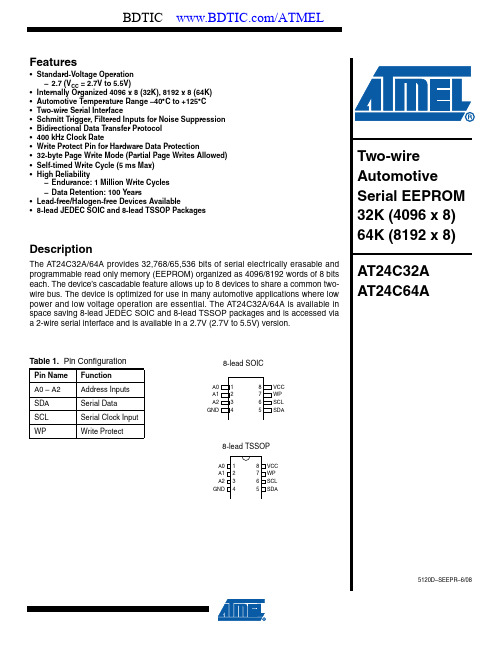
Features•Standard-Voltage Operation –2.7 (V CC = 2.7V to 5.5V)•Internally Organized 4096 x 8 (32K), 8192 x 8 (64K)•Automotive Temperature Range –40°C to +125°C •Two-wire Serial Interface•Schmitt Trigger, Filtered Inputs for Noise Suppression •Bidirectional Data Transfer Protocol •400 kHz Clock Rate•Write Protect Pin for Hardware Data Protection•32-byte Page Write Mode (Partial Page Writes Allowed)•Self-timed Write Cycle (5 ms Max)•High Reliability–Endurance: 1 Million Write Cycles –Data Retention: 100 Years•Lead-free/Halogen-free Devices Available•8-lead JEDEC SOIC and 8-lead TSSOP PackagesDescriptionThe AT24C32A/64A provides 32,768/65,536 bits of serial electrically erasable and programmable read only memory (EEPROM) organized as 4096/8192 words of 8 bits each. The device’s cascadable feature allows up to 8 devices to share a common two-wire bus. The device is optimized for use in many automotive applications where low power and low voltage operation are essential. The AT24C32A/64A is available in space saving 8-lead JEDEC SOIC and 8-lead TSSOP packages and is accessed via a 2-wire serial interface and is available in a 2.7V (2.7V to 5.5V) version.Table 1. Pin ConfigurationPin Name Function A0 – A2Address InputsSDA Serial Data SCL Serial Clock Input WPWrite Protect8-lead SOIC8-lead TSSOPBDTIC www.BDTIC .com/ATMEL25120D–SEEPR–6/08AT24C32A/64AFigure 1. Block DiagramAbsolute Maximum Ratings*Operating T emperature..................................–55°C to +125°C *NOTICE:Stresses beyond those listed under “Absolute Maximum Ratings” may cause permanent dam-age to the device. This is a stress rating only and functional operation of the device at these or any other conditions beyond those indicated in the operational sections of this specification is not implied. Exposure to absolute maximum rating conditions for extended periods may affect device reliability.Storage T emperature.....................................–65°C to +150°C Voltage on Any Pinwith Respect to Ground....................................–1.0V to +7.0V Maximum Operating Voltage ..........................................6.25V DC Output Current........................................................5.0 mA35120D–SEEPR–6/08AT24C32A/64APin DescriptionSERIAL CLOCK (SCL): The SCL input is used to positive edge clock data into each EEPROM device and negative edge clock data out of each device.SERIAL DATA (SDA): The SDA pin is bidirectional for serial data transfer. This pin is open-drain driven and may be wire-ORed with any number of other open-drain or open collector devices.DEVICE/ADDRESSES (A2, A1, A0): The A2, A1 and A0 pins are device address inputs that are hardwired or left not connected for hardware compatibility with other AT24Cxx devices. When the pins are hardwired, as many as eight 32K/64K devices may be addressed on a single bus system (device addressing is discussed in detail under the Device Addressing section). If the pins are left floating, the A2, A1 and A0 pins will be internally pulled down to GND if the capaci-tive coupling to the circuit board V CC plane is <3 pF. If coupling is >3 pF, Atmel recommends connecting the address pins to GND.WRITE PROTECT (WP): The write protect input, when connected to GND, allows normal write operations. When WP is connected high to V CC , all write operations to the memory are inhibited.If the pin is left floating, the WP pin will be internally pulled down to GND if the capacitive cou-pling to the circuit board V CC plane is <3 pF. If coupling is >3pF, Atmel recommends connecting the pin to GND. Switching WP to V CC prior to a write operation creates a software write protect function.Memory OrganizationAT24C32A/64A, 32K/64K SERIAL EEPROM: The 32K/64K is internally organized as 128/256pages of 32 bytes each. Random word addressing requires a 12/13-bit data word address.45120D–SEEPR–6/08AT24C32A/64ANote:1.This parameter is characterized and is not 100% tested.IL IH Table 2. Pin Capacitance (1)Applicable over recommended operating range from T A = 25°C, f = 1.0 MHz, V CC = +2.7V to +5.5VSymbol Test ConditionMax Units Conditions C I/O Input/Output Capacitance (SDA)8pF V I/O = 0V C IN Input Capacitance (A 0, A 1, A 2, SCL)6pFV IN = 0VTable 3. DC CharacteristicsApplicable over recommended operating range from: T A = –40°C to +125°C,V CC = +2.7V to +5.5V (unless otherwise noted)Symbol Parameter Test ConditionMin TypMax Units V CC3Supply Voltage 2.75.5V I CC1Supply Current V CC = 5.0V READ at 400 kHz 0.4 1.0mA I CC2Supply Current V CC = 5.0V WRITE at 400 kHz 2.0 3.0mA I SB Standby Current V CC = 2.7V V IN = V CC or V SS1.0 3.0µA V CC = 5.0V 3.0 5.0I LI Input Leakage CurrentV IN = V CC or V SS 0.10 3.0µA I LO Output Leakage Current V OUT = V CC or V SS0.05 3.0µA V IL (1)Input Low Level –0.6V CC x 0.3V V IH (1)Input High Level V CC x 0.7V CC + 0.5V V OL2Output Low LevelV CC = 3.0VI OL = 2.1 mA0.4V V OL1Output Low Level V CC = 1.8V I OL = 0.15 mA 0.2V55120D–SEEPR–6/08AT24C32A/64ANotes: 1.This parameter is ensured by characterization only.Table 4. AC CharacteristicsApplicable over recommended operating range from T A = –40°C to +125°C, V CC = +2.7V to +5.5V, CL = 1 TTL Gate and 100 pF (unless otherwise noted)Symbol ParameterAT24C32A/AT24C64AUnits 2.7V – 5.5VMinMax f SCL Clock Frequency, SCL 400kHz t LOW Clock Pulse Width Low 1.2µs t HIGH Clock Pulse Width High 0.6µs t I Noise Suppression Time (1)50ns t AA Clock Low to Data Out Valid 0.10.9µs t BUF Time the bus must be free before a new transmission can start (1) 1.2µs t HD.ST A Start Hold Time 0.6µs t SU.ST A Start Set-up Time 0.6µs t HD.DA T Data In Hold Time 0µs t SU.DAT Data In Set-up Time 100ns t R (1)Inputs Rise Time 0.3µs t F (1)Inputs Fall Time 300ns t SU.STO Stop Set-up Time 0.6µs t DH Data Out Hold Time 50ns t WRWrite Cycle Time5ms Endurance (1) 5.0V , 25⋅C, Page Mode1M Write Cycles65120D–SEEPR–6/08AT24C32A/64ADevice OperationCLOCK and DATA TRANSITIONS: The SDA pin is normally pulled high with an external device. Data on the SDA pin may change only during SCL low time periods (refer to Data Valid-ity timing diagram). Data changes during SCL high periods will indicate a start or stop condition as defined below.START CONDITION: A high-to-low transition of SDA with SCL high is a start condition which must precede any other command (see Figure 5 on page 8).STOP CONDITION: A low-to-high transition of SDA with SCL high is a stop condition. After a read sequence, the stop command will place the EEPROM in a standby power mode (see Fig-ure 5 on page 8).ACKNOWLEDGE: All addresses and data words are serially transmitted to and from the EEPROM in 8-bit words. The EEPROM sends a zero during the ninth clock cycle to acknowl-edge that it has received each word.STANDBY MODE: The AT24C32A/64A features a low power standby mode which is enabled:a) upon power-up and b) after the receipt of the stop bit and the completion of any internal operations.MEMORY RESET: After an interruption in protocol, power loss or system reset, any two-wire part can be reset by following these steps:(a) Clock up to 9 cycles, (b) look for SDA high in each cycle while SCL is high and then (c) create a start condition as SDA is high.75120D–SEEPR–6/08AT24C32A/64AFigure 2. Bus TimingSCL: Serial Clock, SDA: Serial Data I/OFigure 3. Write Cycle TimingSCL: Serial Clock, SDA: Serial Data I/ONote:1.The write cycle time t WR is the time from a valid stop condition of a write sequence to the end of the internal clear/write cycle.Figure 4.Data Validity85120D–SEEPR–6/08AT24C32A/64AFigure 5. Start and Stop DefinitionFigure 6.Output Acknowledge95120D–SEEPR–6/08AT24C32A/64ADeviceAddressingThe 32K/64K EEPROM requires an 8-bit device address word following a start condition to enable the chip for a read or write operation (see Figure 7 on page 11). The device address word consists of a mandatory one, zero sequence for the first four most significant bits as shown. This is common to all 2-wire EEPROM devices.The 32K/64K uses the three device address bits A2, A1, A0 to allow as many as eight devices on the same bus. These bits must compare to their corresponding hardwired input pins. The A2,A1, and A0 pins use an internal proprietary circuit that biases them to a logic low condition if the pins are allowed to float.The eighth bit of the device address is the read/write operation select bit. A read operation is ini-tiated if this bit is high and a write operation is initiated if this bit is low.Upon a compare of the device address, the EEPROM will output a zero. If a compare is not made, the device will return to standby state.NOISE PROTECTION: Special internal circuitry placed on the SDA and SCL pins prevent small noise spikes from activating the device.DATA SECURITY: The AT24C32A/64A has a hardware data protection scheme that allows the user to write protect the entire memory when the WP pin is at V CC .WriteOperationsBYTE WRITE: A write operation requires two 8-bit data word addresses following the device address word and acknowledgment. Upon receipt of this address, the EEPROM will again respond with a zero and then clock in the first 8-bit data word. Following receipt of the 8-bit data word, the EEPROM will output a zero and the addressing device, such as a microcontroller,must terminate the write sequence with a stop condition. At this time the EEPROM enters an internally-timed write cycle, t WR , to the nonvolatile memory. All inputs are disabled during this write cycle and the EEPROM will not respond until the write is complete (see Figure 8 on page 11).PAGE WRITE: The 32K/64K EEPROM is capable of 32-byte page writes.A page write is initiated the same way as a byte write, but the microcontroller does not send a stop condition after the first data word is clocked in. Instead, after the EEPROM acknowledges receipt of the first data word, the microcontroller can transmit up to 31 more data words. The EEPROM will respond with a zero after each data word received. The microcontroller must ter-minate the page write sequence with a stop condition (see Figure 9 on page 11).The data word address lower five bits are internally incremented following the receipt of each data word. The higher data word address bits are not incremented, retaining the memory page row location. When the word address, internally generated, reaches the page boundary, the fol-lowing byte is placed at the beginning of the same page. If more than 32 data words are transmitted to the EEPROM, the data word address will “roll over” and previous data will be overwritten.ACKNOWLEDGE POLLING: Once the internally-timed write cycle has started and the EEPROM inputs are disabled, acknowledge polling can be initiated. This involves sending a start condition followed by the device address word. The read/write bit is representative of the operation desired. Only if the internal write cycle has completed will the EEPROM respond with a zero, allowing the read or write sequence to continue.105120D–SEEPR–6/08AT24C32A/64AReadOperationsRead operations are initiated the same way as write operations with the exception that the read/write select bit in the device address word is set to one. There are three read operations:current address read, random address read and sequential read.CURRENT ADDRESS READ: The internal data word address counter maintains the last address accessed during the last read or write operation, incremented by one. This address stays valid between operations as long as the chip power is maintained. The address “roll over”during read is from the last byte of the last memory page, to the first byte of the first page. The address “roll over” during write is from the last byte of the current page to the first byte of the same page.Once the device address with the read/write select bit set to one is clocked in and acknowledged by the EEPROM, the current address data word is serially clocked out. The microcontroller does not respond with an input zero but does generate a following stop condition (see Figure 10 on page 11).RANDOM READ: A random read requires a “dummy” byte write sequence to load in the data word address. Once the device address word and data word address are clocked in and acknowledged by the EEPROM, the microcontroller must generate another start condition. The microcontroller now initiates a current address read by sending a device address with the read/write select bit high. The EEPROM acknowledges the device address and serially clocks out the data word. The microcontroller does not respond with a zero but does generate a follow-ing stop condition (see Figure 11 on page 12).SEQUENTIAL READ: Sequential reads are initiated by either a current address read or a ran-dom address read. After the microcontroller receives a data word, it responds with an acknowledge. As long as the EEPROM receives an acknowledge, it will continue to increment the data word address and serially clock out sequential data words. When the memory address limit is reached, the data word address will “roll over” and the sequential read will continue. The sequential read operation is terminated when the microcontroller does not respond with a zero but does generate a following stop condition (see Figure 12 on page 12).115120D–SEEPR–6/08AT24C32A/64AFigure 7. Device AddressFigure 8. Byte WriteFigure 9. Page WriteNotes:1.* = DON’T CARE bits2.† = DON’T CARE bits for the 32KFigure 10.Current Address Read125120D–SEEPR–6/08AT24C32A/64AFigure 11. Random ReadNote: 1.* = DON’T CARE bitsFigure 12.Sequential Read135120D–SEEPR–6/08AT24C32A/64ANotes:1.For2.7V devices used in the 4.5V to 5.5V range, please refer to performance values in the AC and DC Characteristicstables.2.“Q” designates Green package and RoHS Compliant.AT24C32A Ordering Information (1)Ordering Code Package Operation Range A T24C32AN-10SQ-2.7(2)A T24C32A-10TQ-2.7(2)8S18A2Lead-free/Halogen-free/Automotive (–40⋅C to 125⋅C)Package Type8S18-lead, 0.150" Wide, Plastic Gull Wing Small Outline (JEDEC SOIC)8A28-lead, 4.4 mm Body, Plastic Thin Shrink Small Outline Package (TSSOP)Options–2.7Low Voltage (2.7V to 5.5V)145120D–SEEPR–6/08AT24C32A/64ANotes:1.For2.7V devices used in the 4.5V to 5.5V range, please refer to performance values in the AC and DC Characteristicstables.2.“Q” designates Green package and RoHS Compliant.AT24C64A Ordering Information (1)Ordering Code Package Operation Range A T24C64AN-10SQ-2.7(2)A T24C64A-10TQ-2.7(2)8S18A2Lead-free/Halogen-free/Automotive (–40⋅C to 125⋅C)Package Type8S18-lead, 0.150" Wide, Plastic Gull Wing Small Outline (JEDEC SOIC)8A28-lead, 4.4mm Body, Plastic Thin Shrink Small Outline Package (TSSOP)Options–2.7Low Voltage (2.7V to 5.5V)155120D–SEEPR–6/08AT24C32A/64APackage Drawings8S1 – JEDEC SOIC165120D–SEEPR–6/08AT24C32A/64A8A2 – TSSOP175120D–SEEPR–6/08AT24C32A/64ARevision HistoryRevision HistoryRevision Date Comments5120D6/2008Implemented revision history.。
AT24C1024W-10SI-2.7中文资料

1Features•Low-voltage Operation –2.7 (V CC = 2.7V to 5.5V)•Internally Organized 131,072 x 8•2-wire Serial Interface•Schmitt Triggers, Filtered Inputs for Noise Suppression •Bi-directional Data Transfer Protocol•400 kHz (2.7V) and 1 MHz (5V) Clock Rate•Write Protect Pin for Hardware and Software Data Protection •256-byte Page Write Mode (Partial Page Writes Allowed)•Random and Sequential Read Modes •Self-timed Write Cycle (5 ms Typical)•High Reliability–Endurance: 100,000 Write Cycles/Page –Data Retention: 40 Years•8-lead PDIP , 8-lead EIAJ SOIC, 8-lead LAP and 8-ball dBGA TM PackagesDescriptionThe AT24C1024 provides 1,048,576 bits of serial electrically erasable and program-mable read only memory (EEPROM) organized as 131,072 words of 8 bits each. The device’s cascadable feature allows up to 2 devices to share a common 2-wire bus. The device is optimized for use in many industrial and commercial applications where low-power and low-voltage operation are essential. The devices are available in space-saving 8-lead PDIP, 8-lead EIAJ SOIC, 8-lead Leadless Array (LAP) and 8-ball dBGA packages. In addition, the entire family is available in 2.7V (2.7V to 5.5V) versions.Pin ConfigurationsPin Name Function A1Address Input SDA Serial Data SCL Serial Clock Input WPWrite Protect NCNo Connect8-lead PDIP8-lead Leadless ArrayBottom View8-lead SOIC8-ball dBGABottom View2AT24C10241471H–SEEPR–03/03Block DiagramAbsolute Maximum Ratings*Operating Temperature..................................-55°C to +125°C *NOTICE:Stresses beyond those listed under “Absolute Maximum Ratings” may cause permanent dam-age to the device. This is a stress rating only and functional operation of the device at these or any other conditions beyond those indicated in the operational sections of this specification is not implied. Exposure to absolute maximum rating conditions for extended periods may affect device reliability.Storage Temperature.....................................-65°C to +150°C Voltage on Any Pinwith Respect to Ground.....................................-1.0V to +7.0V Maximum Operating Voltage ..........................................6.25V DC Output Current........................................................5.0 mA3AT24C10241471H–SEEPR–03/03Pin DescriptionSERIAL CLOCK (SCL): The SCL input is used to positive edge clock data into each EEPROM device and negative edge clock data out of each device.SERIAL DATA (SDA): The SDA pin is bi-directional for serial data transfer. This pin is open-drain driven and may be wire-ORed with any number of other open-drain or open-collector devices.DEVICE/PAGE ADDRESSES (A1): The A1 pin is a device address input that can be hard-wired or left not connected for hardware compatibility with AT24C128/256/512. When the A1pin is hardwired, as many as two 1024K devices may be addressed on a single bus system (device addressing is discussed in detail under the Device Addressing section). When the pin is not hardwired, the default A1 is zero.WRITE PROTECT (WP): The hardware Write Protect pin is useful for protecting the entire contents of the memory from inadvertent write operations. The write-protect input, when tied to GND, allows normal write operations. When WP is tied high to V CC , all write operations to the memory are inhibited. If left unconnected, WP is internally pulled down to GND. Switching WP to V CC prior to a write operation creates a software write-protect function.Memory OrganizationAT24C1024, 1024K SERIAL EEPROM: The 1024K is internally organized as 512 pages of 256 bytes each. Random word addressing requires a 17-bit data word address.4AT24C10241471H–SEEPR–03/03Pin Capacitance (1)Note:1.This parameter is characterized and is not 100% tested.DC CharacteristicsNote:1.V IL min and V IH max are reference only and are not tested.Applicable over recommended operating range from T A = 25°C, f = 1.0 MHz, V CC = +2.7V.Symbol Test ConditionMax Units Conditions C I/O Input/Output Capacitance (SDA)8pF V I/O = 0V C IN Input Capacitance (A 1, SCL)6pFV IN = 0VApplicable over recommended operating range from: T AI = -40°C to +85°C, V CC = +2.7V to +5.5V, T AC = 0°C to +70°C,V CC = +2.7V to +5.5V (unless otherwise noted).Symbol Parameter Test ConditionMin TypMax Units V CC Supply Voltage 2.75.5V I CC Supply Current V CC = 5.0V READ at 400 kHz 2.0mA I CC Supply Current V CC = 5.0V WRITE at 400 kHz 5.0mA I SB Standby Current V CC = 2.7V V IN = V CC or V SS3.0µA V CC = 5.5V 6.0µA I LI Input Leakage Current V IN = V CC or V SS 0.10 3.0µA I LO Output Leakage CurrentV OUT = V CC or V SS0.053.0µA V IL Input Low Level (1)-0.6V CC x 0.3V V IH Input High Level (1)V CC x 0.7V CC + 0.5V V OL Output Low LevelV CC = 3.0VI OL = 2.1 mA0.4V5AT24C10241471H–SEEPR–03/03AC Characteristics2.AC measurement conditions:R L (connects to V CC ): 1.3 k Ω (2.7V , 5V)Input pulse voltages: 0.3 V CC to 0.7 V CC Input rise and fall times: ≤50 nsInput and output timing reference voltages: 0.5 V CCApplicable over recommended operating range from T A = -40°C to +85°C, V CC = +2.7V to +5.5V, C L = 100 pF (unless otherwise noted). Test conditions are listed in Note 2.Symbol ParameterTest Conditions MinMax Units f SCL Clock Frequency, SCL 4.5V ≤ V CC ≤ 5.5V 2.7V ≤ V CC ≤ 5.5V 1000400kHz t LOW Clock Pulse Width Low 4.5V ≤ V CC ≤ 5.5V 2.7V ≤ V CC ≤ 5.5V 0.41.3µs t HIGH Clock Pulse Width High 4.5V ≤ V CC ≤ 5.5V 2.7V ≤ V CC ≤ 5.5V 0.40.6µs t AA Clock Low to Data Out Valid4.5V ≤ V CC ≤5.5V 2.7V ≤ V CC ≤ 5.5V 0.050.050.550.9µs t BUF Time the bus must be free before a new transmission can start (1) 4.5V ≤ V CC ≤ 5.5V 2.7V ≤ V CC ≤ 5.5V 0.51.3µs t HD.STA Start Hold Time 4.5V ≤ V CC ≤ 5.5V 2.7V ≤ V CC ≤ 5.5V 0.250.6µs t SU.STA Start Setup Time 4.5V ≤ V CC ≤ 5.5V 2.7V ≤ V CC ≤ 5.5V0.250.6µs t HD.DAT Data In Hold Time 0µs t SU.DA T Data In Setup Time 100ns t R Inputs Rise Time (1)0.3µs t F Inputs Fall Time (1) 4.5V ≤ V CC ≤ 5.5V 2.7V ≤ V CC ≤ 5.5V 100300ns t SU.STO Stop Setup Time 4.5V ≤ V CC ≤ 5.5V 2.7V ≤ V CC ≤ 5.5V0.250.6µs t DH Data Out Hold Time 50ns t WRWrite Cycle Time10ms Endurance (1) 5.0V , 25°C, Page Mode100KWrite Cycles6AT24C10241471H–SEEPR–03/03Device OperationCLOCK and DATA TRANSITIONS: The SDA pin is normally pulled high with an external device. Data on the SDA pin may change only during SCL low time periods (refer to Data Validity timing diagram). Data changes during SCL high periods will indicate a start or stop condition as defined below.START CONDITION: A high-to-low transition of SDA with SCL high is a start condition which must precede any other command (refer to Start and Stop Definition timing diagram).STOP CONDITION: A low-to-high transition of SDA with SCL high is a stop condition. After a read sequence, the Stop command will place the EEPROM in a standby power mode (refer to Start and Stop Definition timing diagram).ACKNOWLEDGE: All addresses and data words are serially transmitted to and from the EEPROM in 8-bit words. The EEPROM sends a zero during the ninth clock cycle to acknowl-edge that it has received each word.STANDBY MODE: The AT24C1024 features a low-power standby mode which is enabled: a)upon power-up and b)after the receipt of the STOP bit and the completion of any internal operations.MEMORY RESET: After an interruption in protocol, power loss or system reset, any 2-wire part can be reset by following these steps:1.Clock up to 9 cycles,2.Look for SDA high in each cycle while SCL is high.3.Create a start condition.7AT24C10241471H–SEEPR–03/03Bus Timing (SCL: Serial Clock, SDA: Serial Data I/O)Write Cycle Timing (SCL: Serial Clock, SDA: Serial Data I/O)Note:1.The write cycle time t WRis the time from a valid stop condition of a write sequence to the end of the internal clear/write cycle.8AT24C10241471H–SEEPR–03/03Data ValidityStart and Stop DefinitionOutput Acknowledge9AT24C10241471H–SEEPR–03/03DeviceAddressingThe 1024K EEPROM requires an 8-bit device address word following a start condition to enable the chip for a read or write operation (refer to Figure 1). The device address word con-sists of a mandatory one, zero sequence for the first five most significant bits as shown. This is common to all 2-wire EEPROM devices.The 1024K uses the one device address bit, A1, to allow up to two devices on the same bus.The A1 bit must compare to the corresponding hardwired input pin. The A1 pin uses an inter-nal proprietary circuit that biases it to a logic low condition if the pin is allowed to float.The seventh bit (P 0) of the device address is a memory page address bit. This memory page address bit is the most significant bit of the data word address that follows. The eighth bit of the device address is the read/write operation select bit. A read operation is initiated if this bit is high and a write operation is initiated if this bit is low.Upon a compare of the device address, the EEPROM will output a zero. If a compare is not made, the device will return to a standby state.DATA SECURITY: The AT24C1024 has a hardware data protection scheme that allows the user to write-protect the entire memory when the WP pin is at V CC .WriteOperationsBYTE WRITE: To select a data word in the 1024K memory requires a 17-bit word address.The word address field consists of the P 0 bit of the device address, then the most significant word address followed by the least significant word address (refer to Figure 2)A write operation requires the P 0 bit and two 8-bit data word addresses following the device address word and acknowledgment. Upon receipt of this address, the EEPROM will again respond with a zero and then clock in the first 8-bit data word. Following receipt of the 8-bit data word, the EEPROM will output a zero. The addressing device, such as a microcontroller,then must terminate the write sequence with a stop condition. At this time the EEPROM enters an internally timed write cycle, T WR , to the nonvolatile memory. All inputs are disabled during this write cycle and the EEPROM will not respond until the write is complete (refer to Figure 2).PAGE WRITE: The 1024K EEPROM is capable of 256-byte page writes.A page write is initiated the same way as a byte write, but the microcontroller does not send a stop condition after the first data word is clocked in. Instead, after the EEPROM acknowledges receipt of the first data word, the microcontroller can transmit up to 255 more data words. The EEPROM will respond with a zero after each data word received. The microcontroller must ter-minate the page write sequence with a stop condition (refer to Figure 3).The data word address lower 8 bits are internally incremented following the receipt of each data word. The higher data word address bits are not incremented, retaining the memory page row location. When the word address, internally generated, reaches the page boundary, the following byte is placed at the beginning of the same page. If more than 256 data words are transmitted to the EEPROM, the data word address will “roll over” and previous data will be overwritten. The address “rollover” during write is from the last byte of the current page to the first byte of the same page.ACKNOWLEDGE POLLING: Once the internally timed write cycle has started and the EEPROM inputs are disabled, acknowledge polling can be initiated. This involves sending a start condition followed by the device address word. The read/write bit is representative of the operation desired. Only if the internal write cycle has completed will the EEPROM respond with a zero, allowing the read or write sequence to continue.10AT24C10241471H–SEEPR–03/03ReadOperationsRead operations are initiated the same way as write operations with the exception that the read/write select bit in the device address word is set to one. There are three read operations:current address read, random address read and sequential read.CURRENT ADDRESS READ: The internal data word address counter maintains the last address accessed during the last read or write operation, incremented by one. This address stays valid between operations as long as the chip power is maintained. The address “rollover”during read is from the last byte of the last memory page, to the first byte of the first page.Once the device address with the read/write select bit set to one is clocked in and acknowl-edged by the EEPROM, the current address data word is serially clocked out. The microcontroller does not respond with an input zero but does generate a following stop condi-tion (refer to Figure 4).RANDOM READ: A random read requires a “dummy” byte write sequence to load in the data word address. Once the device address word and data word address are clocked in and acknowledged by the EEPROM, the microcontroller must generate another start condition.The microcontroller now initiates a current address read by sending a device address with the read/write select bit high. The EEPROM acknowledges the device address and serially clocks out the data word. The microcontroller does not respond with a zero but does generate a fol-lowing stop condition (refer to Figure 5).SEQUENTIAL READ: Sequential reads are initiated by either a current address read or a ran-dom address read. After the microcontroller receives a data word, it responds with an acknowledge. As long as the EEPROM receives an acknowledge, it will continue to increment the data word address and serially clock out sequential data words. When the memory address limit is reached, the data word address will “roll over” and the sequential read will con-tinue. The sequential read operation is terminated when the microcontroller does not respond with a zero, but does generate a following stop condition (refer to Figure 6).11AT24C10241471H–SEEPR–03/03Figure 1. Device AddressFigure 2. Byte WriteFigure 3. Page WriteFigure 4.Current Address Read12AT24C10241471H–SEEPR–03/03Figure 5. Random ReadFigure 6.Sequential Read13AT24C10241471H–SEEPR–03/03Note:For 2.7V devices used in the 4.5V to 5.5V range, please refer to performance values in the AC and DC Characteristics tables.Ordering InformationOrdering CodePackage Operation RangeA T24C1024-10CI-2.7A T24C1024C1-10CI-2.7A T24C1024-10PI-2.7A T24C1024W-10SI-2.7A T24C1024-10UI-2.78CN38CN18P38S28U8Industrial (-40°C to 85°C)Package Type8CN38-lead, 0.230" Wide, Leadless Array Package (LAP)8CN18-lead, 0.300" Wide, Leadless Array Package (LAP)8P38-lead, 0.300" Wide, Plastic Dual In-line Package (PDIP)8S28-lead, 0.200" Wide, Plastic Gull Wing Small Outline Package (EIAJ SOIC)8U88-ball, die Ball Grid Array Package (dBGA)Options-2.7Low Voltage (2.7V to 5.5V)14AT24C10241471H–SEEPR–03/03Packaging Information8CN3 – LAP15AT24C10241471H–SEEPR–03/038CN1 – LAP16AT24C10241471H–SEEPR–03/038P3 – PDIP17AT24C10241471H–SEEPR–03/038S2 – EIAJ SOIC18AT24C10241471H–SEEPR–03/038U8 – dBGA1471H–SEEPR–03/03xMDisclaimer: Atmel Corporation makes no warranty for the use of its products, other than those expressly contained in the Company’s standard warranty which is detailed in Atmel’s Terms and Conditions located on the Company’s web site. The Company assumes no responsibility for any errors which may appear in this document, reserves the right to change devices or specifications detailed herein at any time without notice, and does not make any commitment to update the information contained herein. No licenses to patents or other intellectual property of Atmel are granted by the Company in connection with the sale of Atmel products, expressly or by implication. Atmel’s products are not authorized for use as critical components in life support devices or systems.Atmel CorporationAtmel Operations2325 Orchard Parkway San Jose, CA 95131Tel: 1(408) 441-0311Fax: 1(408) 487-2600Regional HeadquartersEuropeAtmel SarlRoute des Arsenaux 41Case Postale 80CH-1705 Fribourg SwitzerlandTel: (41) 26-426-5555Fax: (41) 26-426-5500AsiaRoom 1219Chinachem Golden Plaza 77 Mody Road Tsimshatsui East Kowloon Hong KongTel: (852) 2721-9778Fax: (852) 2722-1369Japan9F, Tonetsu Shinkawa Bldg.1-24-8 ShinkawaChuo-ku, Tokyo 104-0033JapanTel: (81) 3-3523-3551Fax: (81) 3-3523-7581Memory2325 Orchard Parkway San Jose, CA 95131Tel: 1(408) 441-0311Fax: 1(408) 436-4314Microcontrollers2325 Orchard Parkway San Jose, CA 95131Tel: 1(408) 441-0311Fax: 1(408) 436-4314La Chantrerie BP 7060244306 Nantes Cedex 3, France Tel: (33) 2-40-18-18-18Fax: (33) 2-40-18-19-60ASIC/ASSP/Smart CardsZone Industrielle13106 Rousset Cedex, France Tel: (33) 4-42-53-60-00Fax: (33) 4-42-53-60-011150 East Cheyenne Mtn. Blvd.Colorado Springs, CO 80906Tel: 1(719) 576-3300Fax: 1(719) 540-1759Scottish Enterprise Technology Park Maxwell BuildingEast Kilbride G75 0QR, Scotland Tel: (44) 1355-803-000Fax: (44) 1355-242-743RF/AutomotiveTheresienstrasse 2Postfach 353574025 Heilbronn, Germany Tel: (49) 71-31-67-0Fax: (49) 71-31-67-23401150 East Cheyenne Mtn. Blvd.Colorado Springs, CO 80906Tel: 1(719) 576-3300Fax: 1(719) 540-1759Biometrics/Imaging/Hi-Rel MPU/High Speed Converters/RF DatacomAvenue de Rochepleine BP 12338521 Saint-Egreve Cedex, France Tel: (33) 4-76-58-30-00Fax: (33) 4-76-58-34-80e-mailliterature@Web Site© Atmel Corporation 2003. All rights reserved. Atmel ® and combinations thereof, are the registered trademarks, and dBG A ™ is the trademark of Atmel Corporation or its subsidiaries. Other terms and product names may be the trademarks of others.。
AT24Cxx中文数据手册
AT24C01A/02/04/08A/16A提供1024/2048/4096/8192/16384个连续的可擦除的位,以及由每8位组成一个字节的可编程只读存储器(EEPROM),其分别提供128/256/512/1024/2048个字节。
该设备适用在许多低功耗和低电压操作的工业和商业应用中。
1引脚描述1.1串行时钟(SCL)SCL输入用于正向输出边缘时钟信号到每个EEPROM设备,以及每个设备输出的反向边缘时钟数据。
1.2串行数据(SDA)SDA引脚是用于串行数据双向传输。
该引脚为开漏输出,同时可以与其他开漏极或集电极开路器件进行线或。
1.3设备/页地址(A2,A1,A0)对于AT24C01A和AT24C02,A2、A1和A0引脚是配置器件的硬件地址输入。
一根总线上可以连接多达八个1K / 2K的设备(器件寻址部分详细讨论了器件寻址)。
AT24C04使用A2和A1引脚作为硬件地址输入,在一根总线上有4个4K 的设备可用来寻址。
A0引脚没有连接。
AT24C08A只使用A2引脚作为硬件地址输入,在一根总线上有2个8K 的设备可用来寻址。
A0和A1引脚没有连接。
AT24C16A不使用设备地址引脚,这限制了一根总线上只能挂一个设备。
A0、A1和A2引脚没有连接。
1.4写保护(WP)AT24C01A / 02 / 04 / 08A/ 16A有一个写保护引脚,提供硬件数据保护。
写保护引脚允许正常读/写操作时连接到GND。
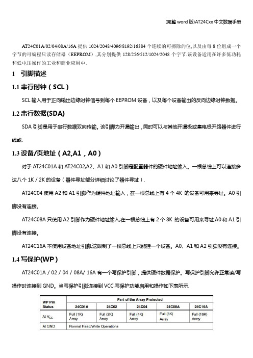
当写保护引脚连接到VCC,写保护功能启用和操作如下表所示。
2设备操作2.1时钟和数据转换SDA引脚通常情况下拉高。
SDA引脚上的数据只能在SCL低时间段内更改,而启动条件或停止条件在SCL为高时进行。
2.2启动条件在任何其他指令之前,SDA由高变为低,且SCL为高。
2.3停止条件SDA由低变为高,且SCL为高。
在读取序列之后,执行停止命令后EEPROM进入备用电源模式。
2.4应答所有地址和数据字都是从EEPROM串行发送和接收8位字节。
AT24C01ASC中文资料
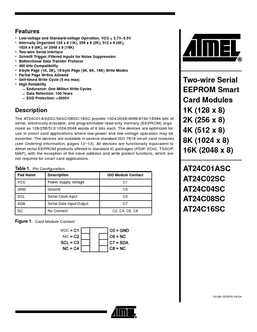
1Features•Low-voltage and Standard-voltage Operation, VCC = 2.7V–5.5V •Internally Organized 128 x 8 (1K), 256 x 8 (2K), 512 x 8 (4K),1024 x 8 (8K), or 2048 x 8 (16K)•Two-wire Serial Interface•Schmitt Trigger, Filtered Inputs for Noise Suppression •Bidirectional Data Transfer Protocol •400 kHz Compatibility•8-byte Page (1K, 2K), 16-byte Page (4K, 8K, 16K) Write Modes •Partial Page Writes Allowed•Self-timed Write Cycle (5 ms max)•High Reliability–Endurance: One Million Write Cycles –Data Retention: 100 Years –ESD Protection: >3000VDescriptionThe AT24C01A/02SC/04SC/08SC/16SC provide 1024/2048/4096/8192/16384 bits of serial, electrically-erasable, and programmable read-only memory (EEPROM) orga-nized as 128/256/512/1024/2048 words of 8 bits each. The devices are optimized for use in smart card applications where low-power and low-voltage operation may be essential. The devices are available in several standard ISO 7816 smart card modules (see Ordering Information, pages 12–13). All devices are functionally equivalent to Atmel serial EEPROM products offered in standard IC packages (PDIP , SOIC, TSSOP ,MAP), with the exception of the slave address and write protect functions, which are not required for smart card applications.Figure 1. Card Module Contact2AT24C01ASC/02SC/04SC/08SC/16SC1610B –SEEPR –04/04Figure 2. Block DiagramPin DescriptionSERIAL CLOCK (SCL): The SCL input is used to positive edge clock data into each EEPROM device and negative edge clock data out of each device.SERIAL DATA (SDA): The SDA pin is bidirectional for serial data transfer. This pin is open-drain driven and may be wire-ORed with any number of other open-drain or open-collector devices.Memory OrganizationAT24C01ASC, 1K SERIAL EEPROM: Internally organized with 16 pages of 8 bytes each, the 1K requires a 7-bit data word address for random word addressing.AT24C02SC, 2K SERIAL EEPROM: Internally organized with 32 pages of 8 bytes each, the 2K requires an 8-bit data word address for random word addressing.Absolute Maximum Ratings*NOTICE:Stresses beyond those listed under “Absolute Maximum Ratings ” may cause permanent dam-age to the device. This is a stress rating only and functional operation of the device at these or any other conditions beyond those indicated in the operational sections of this specification is not implied. Exposure to absolute maximum rating conditions for extended periods may affect device reliability.3AT24C01ASC/02SC/04SC/08SC/16SC1610B –SEEPR –04/04AT24C04SC, 4K SERIAL EEPROM: Internally organized with 32 pages of 16 bytes each, the 4K requires a 9-bit data word address for random word addressing.AT24C08SC, 8K SERIAL EEPROM: Internally organized with 64 pages of 16 bytes each, the 8K requires a 10-bit data word address random word addressing.AT24C16SC, 16K SERIAL EEPROM: Internally organized with 128 pages of 16 bytes each, the 16K requires an 11-bit data word address random word addressing.Pin CapacitanceDC CharacteristicsAC CC 2.V IL min and V IH max are reference only and are not tested.AC CharacteristicsTable 2. Pin Capacitance (1)Applicable over recommended operating range from T = 25°C, f = 1.0 MHz, V = +2.7VTable 3. DC Characteristics (1)(1)4AT24C01ASC/02SC/04SC/08SC/16SC1610B –SEEPR –04/04A CC (unless otherwise noted)2.This parameter is characterized and is not 100% tested.Device OperationCLOCK AND DATA TRANSITIONS: The SDA pin is normally pulled high with an exter-nal device. Data on the SDA pin may change only during SCL-low time periods (see Figure 3 on page 5). Data changes during SCL-high periods will indicate a start or stop condition as defined below.START CONDITION: A high-to-low transition of SDA with SCL high is a start condition that must precede any other command (see Figure 4 on page 6).STOP CONDITION: A low-to-high transition of SDA with SCL high is a stop condition.After a read sequence, the Stop command will place the EEPROM in a standby power mode (see Figure 4 on page 6).ACKNOWLEDGE: All addresses and data words are serially transmitted to and from the EEPROM in 8-bit words. Each word requires the receiver to acknowledge that it has received a valid command or data byte. During the transmission of commands from the host to the EEPROM, the EEPROM will send a zero to the host to acknowledge that it has received a valid command byte. This occurs on the ninth clock cycle of the com-mand byte. During read operations, the host will send a zero to the EEPROM to acknowledge that it has received a valid data byte and that it requests the next sequen-tial data byte to be transmitted during the subsequent eight clock cycles. This occurs on the ninth clock cycle of the data byte. If the host does not transmit this acknowledge bit,the EEPROM will disable the read operation and return to standby mode.STANDBY MODE: The AT24C01ASC/02SC/04SC/08SC/16SC feature a low-power standby mode that is enabled upon power-up and after the receipt of the stop bit and the completion of any internal operations.MEMORY RESET: After an interruption in protocol, power loss, or system reset, any two-wire part can be reset by following these steps:1.Clock up to 9 cycles.2.Look for SDA high in each cycle while SCL is high.3.Create a start condition as SDA is high.Table 4. AC Characteristics (1) (Continued)5AT24C01ASC/02SC/04SC/08SC/16SC1610B –SEEPR –04/04Timing DiagramsBus TimingFigure 1. Bus TimingNote:SCL: Serial Clock, SDA: Serial Data I/OWrite Cycle TimingFigure 2. Write Cycle TimingNotes:1.The write cycle time t WR is the time from a valid stop condition of a write sequence tothe end of the internal clear/write cycle.2.SCL: Serial Clock, SDA: Serial Data I/OData ValidityFigure 3.Data Validity6AT24C01ASC/02SC/04SC/08SC/16SC1610B –SEEPR –04/04Start and Stop DefinitionFigure 4. Start and Stop DefinitionOutput AcknowledgeFigure 5.Output Acknowledge7AT24C01ASC/02SC/04SC/08SC/16SC1610B –SEEPR –04/04Device AddressingThe 1K, 2K, 4K, 8K, and 16K EEPROM devices all require an 8-bit device address word following a start condition to enable the chip for a read or write operation (see Figure 6on page 7).The device address word consists of a mandatory “1”, “0”, “1”, “0” sequence for the first four most significant bits as shown. This is common to all the serial EEPROM devices.The next three bits of the device address word are the most significant data word address bits for the AT24C16SC (16K), which requires a total of 11 address bits. The AT24C08SC (8K) requires only 10 total word address bits. The most significant two bits are included in the device address word. The unused bit of the device address word should be set to “0”. The AT24C04SC (4K) requires only nine total data word address bits. The most significant bit is included in the device address word. The two unused bits of the device address word should be set to “0”. The AT24C02SC (2K) and AT24C01ASC (1K) do not require any address bits in the device address word. The three unused bits of the device address word should be set to “0”.The eighth bit of the device address is the read/write operation select bit. A read opera-tion is initiated if this bit is high, and a write operation is initiated if this bit is low.Upon a compare of the device address, the EEPROM will output a “0” (ACK). If a suc-cessful compare is not made, the chip will return to a standby state (NO ACK).Figure 6. Device AddressNote:P0, P1, P2 = Data word address bits8AT24C01ASC/02SC/04SC/08SC/16SC1610B –SEEPR –04/04Write OperationsBYTE WRITE: A write operation requires an 8-bit data word address following the device address word and acknowledgment. Upon receipt of this address, the EEPROM will again respond with a “0” (ACK) and then clock in the first 8-bit data word. Following receipt of the 8-bit data word, the EEPROM will output a “0” (ACK) and the addressing device, such as a microcontroller, must terminate the write sequence with a stop condi-tion. At this time the EEPROM enters an internally-timed write cycle, t WR , to the nonvolatile memory. All inputs are disabled during this write cycle and the EEPROM will not respond until the write is complete (refer to Figure 7).Figure 7. Byte WritePAGE WRITE: The 1K/2K EEPROM is capable of an 8-byte page write, and the 4K, 8K,and 16K devices are capable of 16-byte page writes.A page write is initiated the same as a byte write, but the microcontroller does not send a stop condition after the first data word is clocked in. Instead, after the EEPROM acknowledges receipt of the first data word, the microcontroller can transmit up to 7(1K/2K) or 15 (4K, 8K, 16K) more data words. The EEPROM will respond with a “0”(ACK) after each data word received. The microcontroller must terminate the page write sequence with a stop condition (refer to Figure 8).Figure 8. Page WriteNote:* = DON ’T CARE bit for 1KThe data word address lower three (1K/2K) or four (4K, 8K, 16K) bits are internally incremented following the receipt of each data word. The higher data word address bits are not incremented, retaining the memory page row location. When the word address,internally generated, reaches the page boundary, the following byte is placed at the beginning of the same page. If more than eight (1K/2K) or 16 (4K, 8K, 16K) data words are transmitted to the EEPROM, the data word address will “roll over ” and previous data will be overwritten.ACKNOWLEGE POLLING: Once the internally timed write cycle has started and the EEPROM inputs are disabled, acknowledge polling can be initiated. This involves send-ing a start condition followed by the device address word. The read/write bit is representative of the operation desired. Only if the internal write cycle has completed9AT24C01ASC/02SC/04SC/08SC/16SC1610B –SEEPR –04/04will the EEPROM respond with a “0” (ACK), allowing the read or write sequence to continue.Read OperationsRead operations are initiated the same way as write operations, with the exception that the read/write select bit in the device address word is set to “1”. There are three read operations: current address read, random address read, and sequential read.CURRENT ADDRESS READ: The internal data word address counter maintains the last address accessed during the last read or write operation, incremented by one. This address stays valid between operations as long as the chip power is maintained. The address “rollover ” during read is from the last byte of the last memory page to the first byte of the first page. The address “rollover ” during write is from the last byte of the cur-rent page to the first byte of the same page.Once the device address with the read/write select bit set to “1” is clocked in and acknowledged by the EEPROM, the current address data word is serially clocked out.The microcontroller does not respond with an input “0” but does generate a following stop condition (refer to Figure 9)Figure 9. Current Address Read.RANDOM READ: A random read requires a “dummy ” byte write sequence to load in the data word address. Once the device address word and data word address are clocked in and acknowledged by the EEPROM, the microcontroller must generate another start condition. The microcontroller now initiates a current address read by sending a device address with the read/write select bit high. The EEPROM acknowledges the device address and serially clocks out the data word. The microcontroller does not respond with a “0” (NO ACK) but does generate a following stop condition (refer to Figure 10).Figure 10. Random ReadNote:* = DON ’T CARE bit for 1K)10AT24C01ASC/02SC/04SC/08SC/16SC1610B –SEEPR –04/04SEQUENTIAL READ: Sequential reads are initiated by either a current address read or a random address read. After the microcontroller receives a data word, it responds with an acknowledge. As long as the EEPROM receives an acknowledge, it will continue to increment the data word address and serially clock out sequential data words. When the memory address limit is reached, the data word address will “rollover ” and the sequen-tial read will continue. The sequential read operation is terminated when the microcontroller does not respond with a “0” (NO ACK) but does generate a following stop condition (refer to Figure 11).Figure 11.Sequential Read11AT24C01ASC/02SC/04SC/08SC/16SC1610B –SEEPR –04/04AT24C01ASC Ordering InformationAT24C02SC Ordering InformationAT24C04SC Ordering InformationAT24C08SC Ordering InformationAT24C16SC Ordering Information12AT24C01ASC/02SC/04SC/08SC/16SC1610B–SEEPR–04/0413AT24C01ASC/02SC/04SC/08SC/16SC1610B –SEEPR –04/04Smart Card ModulesDisclaimer: Atmel Corporation makes no warranty for the use of its products, other than those expressly contained in the Company ’s standard warranty which is detailed in Atmel ’s Terms and Conditions located on the Company ’s web site. The Company assumes no responsibil ity for any errors which may appear in this document, reserves the right to change devices or specifications detailed herein at any time wit h out notice, and does not make any commitment to update the information contained herein. No licenses to patents or other intellectual property of Atmel are granted by the Company in connection with the sale of Atmel products, expressly or by implication. Atmel ’s products are not auth orized for use as critical components in life support devices or systems.Atmel CorporationAtmel Operations2325 Orchard Parkway San Jose, CA 95131Tel: 1(408) 441-0311Fax: 1(408) 487-2600Regional HeadquartersEuropeAtmel SarlRoute des Arsenaux 41Case Postale 80CH-1705 Fribourg SwitzerlandTel: (41) 26-426-5555Fax: (41) 26-426-5500AsiaRoom 1219Chinachem Golden Plaza 77 Mody Road Tsimshatsui East Kowloon Hong KongTel: (852) 2721-9778Fax: (852) 2722-1369Japan9F, Tonetsu Shinkawa Bldg.1-24-8 ShinkawaChuo-ku, Tokyo 104-0033JapanTel: (81) 3-3523-3551Fax: (81) 3-3523-7581Memory2325 Orchard Parkway San Jose, CA 95131Tel: 1(408) 441-0311Fax: 1(408) 436-4314Microcontrollers2325 Orchard Parkway San Jose, CA 95131Tel: 1(408) 441-0311Fax: 1(408) 436-4314La Chantrerie BP 7060244306 Nantes Cedex 3, France Tel: (33) 2-40-18-18-18Fax: (33) 2-40-18-19-60ASIC/ASSP/Smart CardsZone Industrielle13106 Rousset Cedex, France Tel: (33) 4-42-53-60-00Fax: (33) 4-42-53-60-011150 East Cheyenne Mtn. Blvd.Colorado Springs, CO 80906Tel: 1(719) 576-3300Fax: 1(719) 540-1759Scottish Enterprise Technology Park Maxwell BuildingEast Kilbride G75 0QR, Scotland Tel: (44) 1355-803-000Fax: (44) 1355-242-743RF/AutomotiveTheresienstrasse 2Postfach 353574025 Heilbronn, Germany Tel: (49) 71-31-67-0Fax: (49) 71-31-67-23401150 East Cheyenne Mtn. Blvd.Colorado Springs, CO 80906Tel: 1(719) 576-3300Fax: 1(719) 540-1759Biometrics/Imaging/Hi-Rel MPU/High Speed Converters/RF DatacomAvenue de Rochepleine BP 12338521 Saint-Egreve Cedex, France Tel: (33) 4-76-58-30-00Fax: (33) 4-76-58-34-80e-mailliterature@Web Site1610B –SEEPR –04/04© Atmel Corporation 2003. All rights reserved. Atmel ® and combinations thereof are registered trademarks of Atmel Corporation or its subsidiaries. Other terms and product names may be the trademarks of others.。
AT24c02最全的中文资料

CA T24C 161/162(16K),CAT24C081 /082(8K) CAT24C041/042(4K),CAT24C021/022(2K)I2C串行CMOS E2PROM,精确的复位控制器和看门狗定时器控制电路特性•数据线上的看门狗定时器(仅对CA T24Cxxl)籲可编程复位门槛电平籲高数据传送速率为400KHz和I2C总线兼容• 2.7V至6V的工作电压•低功耗CMOS工艺籲16字节页写缓冲区籲片内防误擦除写保护籲高低电平复位信号输出——精确的电源电压监视器——可选择5V、3.3V和3V的复位门槛电平•100万次擦写周期•数据保存可长达100年•8脚DIP或SOIC封装•商业级、工业级和汽车温度范围概述CA T24Cxxx是集E2PROM存储器,复位微控制器和看门狗定时器三种流行功能与一体的芯片。
CAT24C161/162 (16K),CAT24C081/082 (8K),CA T24C041/042 (4K)和CAT24C021/022 (2K)以I2C是串行CMOS E2PROM器件。
釆用CMOS工艺大降低了器件的功耗。
CA T24Cxxx 另一特点是16字节的页写缓冲区,提供8脚DIP和SOIC 封装。
CA T24Cxxx的复位功能和看门狗定时器功能保证系统出现故障的时候能给CPU —个复位信号。
CA T24Cxxx 的2脚输出低电平复位信号,7脚输出高电平复位信号。
CAT24Cxxl看狗溢出信号从SDA脚输出。
CAT24Cxx2不具备看门狗功能。
绝对最大参数工作温度:-55°C〜125°C贮存温度:-65°C〜15°C各管脚承受对地电压:-2.0V〜Vcc+2.0V VCC对地电压范围:-2.0V〜7.0V 最大功耗: 1.0W管脚焊接温度(10S): 300 °C输出短路电流:100mA管脚配置]V C C ]RESET方框图表一直流操作特性表二上电时序管脚介绍WP:写保护将该管脚接Vcc,E2PRON就实现写保护(只读)。
(完整word版)AT24Cxx中文数据手册
AT24C01A/02/04/08A/16A提供1024/2048/4096/8192/16384个连续的可擦除的位,以及由每8位组成一个字节的可编程只读存储器(EEPROM),其分别提供128/256/512/1024/2048个字节.该设备适用在许多低功耗和低电压操作的工业和商业应用中。
1引脚描述1.1串行时钟(SCL)SCL输入用于正向输出边缘时钟信号到每个EEPROM设备,以及每个设备输出的反向边缘时钟数据。
1.2串行数据(SDA)SDA引脚是用于串行数据双向传输。
该引脚为开漏输出,同时可以与其他开漏极或集电极开路器件进行线或.1.3设备/页地址(A2,A1,A0)对于AT24C01A和AT24C02,A2、A1和A0引脚是配置器件的硬件地址输入。
一根总线上可以连接多达八个1K / 2K的设备(器件寻址部分详细讨论了器件寻址).AT24C04使用A2和A1引脚作为硬件地址输入,在一根总线上有4个4K 的设备可用来寻址。
A0引脚没有连接。
AT24C08A只使用A2引脚作为硬件地址输入,在一根总线上有2个8K 的设备可用来寻址.A0和A1引脚没有连接。
AT24C16A不使用设备地址引脚,这限制了一根总线上只能挂一个设备。
A0、A1和A2引脚没有连接。
1.4写保护(WP)AT24C01A / 02 / 04 / 08A/ 16A有一个写保护引脚,提供硬件数据保护。
写保护引脚允许正常读/写操作时连接到GND。
当写保护引脚连接到VCC,写保护功能启用和操作如下表所示.2设备操作2.1时钟和数据转换SDA引脚通常情况下拉高.SDA引脚上的数据只能在SCL低时间段内更改,而启动条件或停止条件在SCL 为高时进行。
2.2启动条件在任何其他指令之前,SDA由高变为低,且SCL为高。
2.3停止条件SDA由低变为高,且SCL为高。
在读取序列之后,执行停止命令后EEPROM进入备用电源模式.2.4应答所有地址和数据字都是从EEPROM串行发送和接收8位字节。
AT24C512B_08中文资料
AT24C512B_08中文资料FeaturesLow-voltage and Standard-voltage Operation–1.8v (V CC = 1.8V to 3.6V)–2.5v (V CC = 2.5V to 5.5V)?Internally Organized 65,536 x 8?Two-wire Serial InterfaceSchmitt Triggers, Filtered Inputs for Noise Suppression ?Bidirectional Data Transfer Protocol1 MHz (2.5V , 5.5V), 400 kHz (1.8V) CompatibilityWrite Protect Pin for Hardware and Software Data Protection ?128-byte Page Write Mode (Partial Page Writes Allowed)?Self-timed Write Cycle (5 ms Max)?High Reliability–Endurance: 1,000,000 Write Cycles –Data Retention: 40 Years ?Lead-free/Halogen-free Devices8-lead PDIP , 8-lead JEDEC SOIC, 8-lead EIAJ SOIC, 8-lead TSSOP , 8-ball dBGA2, and 8-lead Ultra Thin Small Array (SAP) PackagesDie Sales: Wafer Form, Waffle Pack and Bumped DieDescriptionThe AT24C512B provides 524,288 bits of serial electrically erasable and programma-ble read only memory (EEPROM) organized as 65,536 words of 8 bits each. The device’s cascadable feature allows up to eight devices to share a common two-wire bus. The device is optimized for use in many industrial and commercial applications where low-power and low-voltage operation are essential. The devices are available in space-saving 8-pin PDIP, 8-lead JEDEC SOIC, 8-lead EIAJ SOIC, 8-lead TSSOP,8-ball dBGA2 and 8-lead Ultra Thin SAP packages. In addition, the entire family is available in 1.8V (1.8V to 3.6V) and 2.5V (2.5V to 5.5V) versions.T able 0-1.Pin ConfigurationsPin Name Function A0–A2Address Inputs SDA Serial Data SCL Serial Clock Input WPWrite ProtectRev. 5297A–SEEPR–1/08Two-wire Serial EEPROM512K (65,536 x 8)AT24C512Bwith Three Device Address Inputs8-lead PDIP8-lead TSSOPBottom View8-lead SOIC8-ball dBGA2Bottom View25297A–SEEPR–1/08AT24C512BFigure 0-1.Block Diagram Absolute Maximum Ratings*Operating T emperature..................................–55°C to +125°C *NOTICE:Stresses beyond those listed under “Absolute Maximum Ratings” may cause permanent dam-age to the device. This is a stress rating only and functional operation of the device at these or any other conditions beyond those indicated in the operational sections of this specification is not implied. Exposure to absolute maximum rating conditions for extended periods may affect device reliability.Storage T emperature.....................................–65°C to +150°C Voltage on Any Pinwith Respect to Ground....................................–1.0V to +7.0V Maximum Operating Voltage ..........................................6.25V DC Output Current........................................................5.0 mA35297A–SEEPR–1/08AT24C512B1.Pin DescriptionSERIAL CLOCK (SCL): The SCL input is used to positive edge clock data into each EEPROM device and negative edge clock data out of each device.SERIAL DATA (SDA): The SDA pin is bidirectional for serial data transfer. This pin is open-drain driven and may be wire-ORed with any number of other open-drain or open collector devices.DEVICE/PAGE ADDRESSES (A2, A1, A0): The A2, A1, and A0 pins are device address inputs that are hardwired (directly toGND or to Vcc) for compatibility with other AT24Cxx devices.When the pins are hardwired, as many as eight 512K devices may be addressed on a single bus system. (Device addressing is discussed in detail under “Device Addressing,” page 8.) A device is selected when a corresponding hardware and software match is true. If these pins are left floating, the A2, A1, and A0 pins will be internally pulled down to GND. However, due to capaci-tive coupling that may appear during customer applications, Atmel ? recommends always connecting the address pins to a known state. When using a pull-up resistor, Atmel recommends using 10k Ω or less.WRITE PROTECT (WP): The write protect input, when connected to GND, allows normal write operations. When WP is connected directly to Vcc, all write operations to the memory are inhib-ited. If the pin is left floating, the WP pin will be internally pulled down to GND. However, due to capacitive coupling that may appear during customer applications, Atmel recommends always connecting the WP pins to a known state. When using a pull-up resistor, Atmel rec ommends using 10k Ω or less.45297A–SEEPR–1/08AT24C512B2.Memory OrganizationAT24C512B, 512K SERIAL EEPROM: The 512K is internally organized as 512 pages of 128-bytes each. Random word addressing requires a 16-bit data word address.Note:1.This parameter is characterized and is not 100% tested.Note:1.V IL min and V IH max are reference only and are not tested.Table 2-1.Pin Capacitance (1)Applicable over recommended operating range from: T A = 25°C, f = 1.0 MHz, V CC = +1.8V to +5.5VSymbol Test ConditionMax Units Conditions C I/O Input/Output Capacitance (SDA)8pF V I/O = 0V C IN Input Capacitance (A 0, A 1, SCL) 6pFV IN = 0VTable 2-2.DC CharacteristicsApplicable over recommended operating range from: T AI = –40°C to +85°C, V CC = +1.8V to +5.5V (unless otherwise noted) Symbol Parameter Test ConditionMin TypMax Units V CC1Supply Voltage 1.8 3.6V V CC2Supply Voltage 2.55.5V I CC Supply Current V CC = 5.0V READ at 400 kHz 2.0mAI CC Supply Current V CC = 5.0V WRITE at 400 kHz 3.0mA I SB1Standby CurrentV CC = 1.8V V IN = V CC or V SS1.0μA V CC = 3.6V 3.0μA I SB2Standby Current V CC =2.5V V IN = V CC or V SS2.0μA V CC = 5.5V 6.0μA I LI Input Leakage Current V IN = V CC or V SS 0.10 3.0μA I LO Output Leakage CurrentV OUT = V CC or V SS0.053.0μA V IL Input Low Level (1)–0.6V CC x 0.3V V IH Input High Level (1)V CC x 0.7V CC + 0.5V V OL1Output Low Level V CC = 1.8V I OL = 0.15 mA 0.2V V OL2Output Low LevelV CC = 3.0VI OL = 2.1 mA 0.4V55297A–SEEPR–1/08AT24C512BNotes:1.This parameter is ensured by characterization only.2.AC measurement conditions:R L (connects to V CC ): 1.3 k Ω (2.5V , 5V), 10 k Ω (1.8V)Input pulse voltages: 0.3 V CC to 0.7 V CC Input rise and fall times: ≤ 50 nsInput and output timing reference voltages: 0.5 V CCTable 2-3.AC Characteristics (Industrial Temperature)Applicable over recommended operating range from T AI = ?40°C to +85°C, V CC = +1.8V to +5.5V, CL = 100 pF (unless oth-erwise noted). Test conditions are listed in Note 2.Symbol Parameter1.8-volt2.5, 5.0-volt Units MinMax MinMax f SCL Clock Frequency, SCL 4001000kHz t LOW Clock Pulse Width Low 1.30.4μs t HIGH Clock Pulse Width High 0.60.4μs t i Noise Suppression Time (1)10050ns t AA Clock Low toData Out Valid 0.050.90.050.55μs t BUF Time the bus must be free before a new transmission can start (1) 1.30.5μs t HD.ST A Start Hold Time 0.60.25μs t SU.ST A Start Set-up Time 0.60.25μs t HD.DA T Data In Hold Time 00μs t SU.DAT Data In Set-up Time 100 100ns t R Inputs Rise Time (1)0.30.3μs t F Inputs Fall Time (1)300 100ns t SU.STO Stop Set-up Time 0.60.25μs t DH Data Out Hold Time 5050ns t WRWrite Cycle Time 55ms Endurance (1)25°C, Page Mode, 3.3V1,000,000Write Cycles65297A–SEEPR–1/08AT24C512B3.Device OperationCLOCK and DATA TRANSITIONS: The SDA pin is normally pulled high with an external device.Data on the SDA pin may change only during SCL low time periods (see Figure 3-4 on page 8).Data changes during SCL high periods will indicate a start or stop condition as defined below.START CONDITION: A high-to-low transition of SDA with SCL high is a start condition which must precede any other command (see Figure 3-5 on page 8).STOP CONDITION: A low-to-high transition of SDA with SCLhigh is a stop condition. After a read sequence, the stop command will place the EEPROM in a standby power mode (see Fig-ure 3-5 on page 8).ACKNOWLEDGE: All addresses and data words are serially transmitted to and from the EEPROM in 8-bit words. The EEPROM sends a zero during the ninth clock cycle to acknowl-edge that it has received each word.STANDBY MODE: The AT24C512B features a low power standby mode which is enabled: a)upon power-up and b) after the receipt of the STOP bit and the completion of any internal operations.Software Reset: After an interruption in protocol, power loss or system reset, any 2-wire part can be protocol reset by following these steps: (a) Create a start bit condition, (b)clock 9 cycles, (c) create another start bit followed by stop bit condition as shown below.The device is ready for next communication after above steps have been completed.Figure 3-1.Protocol Reset Condition75297A–SEEPR–1/08AT24C512BFigure 3-3.Write Cycle Timing (SCL: Serial Clock, SDA: Serial Data I/O)Note:1.The write cycle time t WRis the time from a valid stop condition of a write sequence to the end of the internal clear/write cycle.85297A–SEEPR–1/08AT24C512BFigure 3-4.Data ValidityFigure 3-5.Start and Stop DefinitionFigure 3-6.Output Acknowledge95297A–SEEPR–1/08AT24C512B4.Device AddressingThe 512K EEPROM requires an 8-bit device address word following a start condition to enable the chip for a read or write operation (see Figure 6-1 on page 10). The device address word con-sists of a mandatory “1”, “0” sequence for the f irst four most significant bits as shown. This is common to all two-wire EEPROM devices.The 512K uses the three device address bits A2, A1, A0 to allow as many as eight devices on the same bus. These bits must compare to their corresponding hardwired input pins. The A2, A1and A0 pins use an internal proprietary circuit that biases them to a logic low condition if the pins are allowed to float.The eighth bit of the device address is the read/writeoperation select bit. A read operation is ini-tiated if this bit is high and a write operation is initiated if this bit is low.Upon a compare of the device address, the EEPROM will output a “0”. If a compare is not made,the device will return to a standby state.DATA SECURITY: The AT24C512B has a hardware data protection scheme that allows the user to Write Protect the whole memory when the WP pin is at V CC .5.Write OperationsBYTE WRITE: A write operation requires two 8-bit data word addresses following the device address word and acknowledgment. Upon receipt of this address, the EEPROM will again respond with a “0” and then clock in the first 8-bit data word. Following receipt of the 8-bit data word, the EEPROM will output a “0”. The addressing device, such as a microcontroller, then must terminate the write sequence with a stop condition. At this time the EEPROM enters an internally-timed write cycle, t WR , to the nonvolatile memory. All inputs are disabled during this write cycle and the EEPROM will not respond until the write is complete (see Figure 6-2 on page 10).PAGE WRITE: The 512K EEPROM is capable of 128-byte page writes.A page write is initiated the same way as a byte write, but the microcontroller does not send a stop condition after the first data word is clocked in. Instead, after the EEPROM acknowledges receipt of the first data word, the microcontroller can transmit up to 127 more data words. The EEPROM will respond with a “0” after each data word received. The microcontroller must termi-nate the page write sequence with a stop condition (see Figure 6-3 on page 11).The data word address lower 7 bits are internally incremented following the receipt of each data word. The higher data word address bits are not incremented, retaining the memory page row location. When the word address, internally generated, reaches the page boundary, the follow-ing byte is placed at the beginning of the same page. If more than 128 data words are transmitted to the EEPROM, the data word address will “roll over” and previous data will be overwritten. The address roll over during write is from the last byte of the current page to the first byte of the same page.ACKNOWLEDGE POLLING: Once the internally-timed write cycle has started and the EEPROM inputs are disabled, acknowledge polling can be initiated. This involves sending a start condition followed by the device address word. The Read/Write bit is representative of the operation desired. Only if the internal write cycle has completed will the EEPROM respond with a “0”, allowing the read or write sequence to continue.105297A–SEEPR–1/08AT24C512B6.Read OperationsRead operations are initiated the same way as write operations with the exception that the Read/Write select bit in the device address word is set to “1”. There are three read operations:current address read, random address read and sequential read.CURRENT ADDRESS READ: The internal data word address counter maintains the last address accessed during the last read or write operation, incremented by “1”. This address stays validbetween operations as long as the chip power is maintained. The address roll over during read is from the last byte of the last memory page, to the first byte of the first page.Once the device address with the Read/Write select bit set to “1” is clocked in and acknowl-edged by the EEPROM, the current address data word is serially clocked out. The microcontroller does not respond with an input “0” but does generate a following stop condition (see Figure 6-4 on page 11).RANDOM READ: A random read requires a “dummy” byte write sequence to load in the data word address. Once the device address word and data word address are clocked in and acknowledged by the EEPROM, the microcontroller must generate another start condition. The microcontroller now initiates a current address read by sending a device address with the Read/Write select bit high. The EEPROM acknowledges the device address and serially clocks out the data word. The microcontroller does not respond with a “0” but does generate a following stop condition (see Figure 6-5 on page 11).SEQUENTIAL READ: Sequential reads are initiated by either a current address read or a ran-dom address read. After the microcontroller receives a data word, it responds with an acknowledge. As long as the EEPROM receives an acknowledge, it will continue to increment the data word address and serially clock out sequential data words. When the memory address limit is reached, the data word address will roll over and the sequential read will continue. The sequential read operation is terminated when the micr ocontroller does not respond with a “0” but does generate a following stop condition (see Figure 6-6 on page 11).Figure 6-1.Device AddressFigure 6-2.Byte Write115297A–SEEPR–1/08AT24C512BFigure 6-3.Page WriteFigure 6-4.Current Address ReadFigure 6-5.Random ReadFigure 6-6.Sequential Read125297A–SEEPR–1/08AT24C512BNotes: 1.“-B” denotes bulk2.“-T” denotes tape and reel. SOIC = 4K per reel. TSSOP and dBGA2 = 5K per reel. SAP = 3K per reel. EIAJ = 2K per reel.3.Available in tape and reel, and wafer form; order as SL788 for inkless wafer form. Bumped die available upon request.Please contact Serial Interface Marketing.Ordering InformationOrdering CodeVoltage Package Operation RangeA T24C512B-PU (Bulk form only) 1.88P3Lead-free/Halogen-free/Industrial Temperature (–40°C to 85°C)A T24C512B-PU25 (Bulk form only) 2.58P3A T24C512BN-SH-B (1) (NiPdAu Lead Finish) 1.88S1A T24C512BN-SH-T (2) (NiPdAu Lead Finish) 1.88S1A T24C512BN-SH25-B (1) (NiPdAu Lead Finish) 2.58S1A T24C512BN-SH25-T (2) (NiPdAu Lead Finish) 2.58S1A T24C512BW-SH-B (1) (NiPdAu Lead Finish) 1.88S2A T24C512BW-SH-T (2) (NiPdAu Lead Finish) 1.88S2A T24C512BW-SH25-B (1) (NiPdAu Lead Finish) 2.58S2A T24C512BW-SH25-T (2) (NiPdAu Lead Finish) 2.58S2A T24C512B-TH-B (1) (NiPdAu Lead Finish) 1.88A2A T24C512B-TH-T (2) (NiPdAu Lead Finish) 1.88A2A T24C512B-TH25-B (1) (NiPdAu Lead Finish) 2.58A2A T24C512B-TH25-T (2) (NiPdAu Lead Finish) 2.58A2A T24C512BY7-YH-T (2) (NiPdAu Lead Finish) 1.88Y7A T24C512BY7-YH25-T (2) (NiPdAu Lead Finish) 2.58Y7A T24C512BU2-UU-T (2) 1.88U2-1A T24C512B-W-11(3)1.8Die SaleIndustrial Temperature (–40°C to 85°C)Package Type8P38-lead, 0.300" Wide, Plastic Dual In-line Package (PDIP) 8S18-lead, 0.150” Wide, Plastic Gull Wing Small Outline Package (JEDEC SOIC)8S28-lead, 0.200” Wide Plastic Gull Wing Small Outline Package (EIAJ SOIC)8A28-lead, 4.4 mm Body, Plastic Thin Shrink Small Outline Package (TSSOP)8Y78-lead, 6.00 mm x 4.90 mm Body, Ultra Thin, Dual Footprint, Non-leaded, Small Array Package (SAP)8U2-1 8-ball, die Ball Grid Array Package (dBGA2)Options–1.8Low-voltage (1.8V to 3.6V)–2.5Low-voltage (2.5V to 5.5V)135297A–SEEPR–1/08AT24C512B7.Part marking scheme:7.18-PDIP(1.8V)7.28-PDIP(2.5V)TOP MARKSeal YearY = SEAL YEARWW = SEAL WEEK | Seal Week6: 2006 0: 2010 02 = Week 2 | | |7: 2007 1: 2011 04 = Week 4 |---|---|---|---|---|---|---|---| 8: 2008 2: 2012 :: : :::: : A T M L U Y W W 9: 2009 3: 2013 :: : :::: :: |---|---|---|---|---|---|---|---| 50 = Week 50 2 F B 152 = Week 52|---|---|---|---|---|---|---|---| * Lot NumberLot Number to Use ALL Characters in Marking |---|---|---|---|---|---|---|---| |BOTTOM MARKPin 1 Indicator (Dot)No Bottom MarkTOP MARKSeal YearY = SEAL YEARWW = SEAL WEEK | Seal Week6: 2006 0: 2010 02 = Week 2 | | |7: 2007 1: 2011 04 = Week 4 |---|---|---|---|---|---|---|---| 8: 2008 2: 2012 :: : :::: : A T M L U Y W W 9: 2009 3: 2013 :: : :::: :: |---|---|---|---|---|---|---|---| 50 = Week 50 2 F B 252 = Week 52|---|---|---|---|---|---|---|---| * Lot NumberLot Number to Use ALL Characters in Marking |---|---|---|---|---|---|---|---| |BOTTOM MARKPin 1 Indicator (Dot)No Bottom Mark145297A–SEEPR–1/08AT24C512B7.38-SOIC(1.8V)7.48-SOIC(2.5V)TOP MARKSeal YearY = SEAL YEARWW = SEAL WEEK | Seal Week6: 2006 0: 2010 02 = Week 2 | | |7: 2007 1: 2011 04 = Week 4 |---|---|---|---|---|---|---|---| 8: 2008 2: 2012 :: : :::: : A T M L H Y W W 9: 2009 3: 2013 :: : :::: :: |---|---|---|---|---|---|---|---| 50 = Week 50 2 F B 152 = Week 52|---|---|---|---|---|---|---|---| * Lot NumberLot Number to Use ALL Characters in Marking |---|---|---|---|---|---|---|---| |BOTTOM MARKPin 1 Indicator (Dot)No Bottom MarkTOP MARKSeal YearY = SEAL YEARWW = SEAL WEEK | Seal Week6: 2006 0: 2010 02 = Week 2 | | |7: 2007 1: 2011 04 = Week 4 |---|---|---|---|---|---|---|---| 8: 2008 2: 2012 :: : :::: : A T M L H Y W W 9: 2009 3: 2013 :: : :::: :: |---|---|---|---|---|---|---|---| 50 = Week 50 2 F B 252 = Week 52|---|---|---|---|---|---|---|---| * Lot NumberLot Number to Use ALL Characters in Marking |---|---|---|---|---|---|---|---| |BOTTOM MARKPin 1 Indicator (Dot)No Bottom Mark155297A–SEEPR–1/08AT24C512B7.58-TSSOP(1.8V)7.68-TSSOP(2.5V)TOP MARKPin 1 Indicator (Dot)Y = SEAL YEAR WW = SEAL WEEK |6: 2006 0: 2010 02 = Week 2 |---|---|---|---| 7: 2007 1: 2011 04 = Week 4 * H Y W W 8: 2008 2: 2012 :: : :::: : |---|---|---|---|---| 9: 2009 3: 2013:: : :::: :: 2 F B 1 * 50 = Week 50|---|---|---|---|---|52 = Week 52BOTTOM MARK|---|---|---|---|---|---|---|Country of originC 0 0|---|---|---|---|---|---|---| A A A A A A A |---|---|---|---|---|---|---| <- Pin 1 IndicatorTOP MARKPin 1 Indicator (Dot)Y = SEAL YEAR WW = SEAL WEEK |6: 2006 0: 2010 02 = Week 2 |---|---|---|---| 7: 2007 1: 2011 04 = Week 4 * H Y W W 8: 2008 2: 2012 :: : :::: : |---|---|---|---|---| 9: 2009 3: 2013:: : :::: :: 2 F B 2 * 50 = Week 50 |---|---|---|---|---| 52 = Week 52BOTTOM MARK|---|---|---|---|---|---|---|Country of originC 0 0|---|---|---|---|---|---|---| A A A A A A A |---|---|---|---|---|---|---| <- Pin 1 Indicator165297A–SEEPR–1/08AT24C512B7.78-Ultra Thin SAP (1.8V)7.88-Ultra Thin SAP (2.5V)TOP MARKSeal Year| Seal Week Y = SEAL YEARWW = SEAL WEEK | | |6: 2006 0: 2010 02 = Week 2 |---|---|---|---|---|---|---|---| 7: 2007 1: 2011 04 = Week 4 A T M L H Y W W 8: 2008 2: 2012 :: : :::: : |---|---|---|---|---|---|---|---| 9: 2009 3: 2013:: : :::: :: 2 F B 150 = Week 50 |---|---|---|---|---|---|---|---| 52 = Week 52Lot Number|---|---|---|---|---|---|---|---| * |Pin 1 Indicator (Dot)TOP MARKSeal Year| Seal Week Y = SEAL YEARWW = SEAL WEEK | | |6: 2006 0: 2010 02 = Week 2 |---|---|---|---|---|---|---|---| 7: 2007 1: 2011 04 = Week 4 A T M L H Y W W 8: 2008 2: 2012 :: : :::: : |---|---|---|---|---|---|---|---| 9: 2009 3: 2013:: : :::: :: 2 F B 250 = Week 50 |---|---|---|---|---|---|---|---| 52 = Week 52Lot Number|---|---|---|---|---|---|---|---| * |Pin 1 Indicator (Dot)175297A–SEEPR–1/08AT24C512B7.8dBGA2TOP MARKLINE 1-------> 2FBU LINE 2-------> YMTC|<-- Pin 1 This Corner P = Country of OriginY = ONE DIGIT YEAR CODE 4: 2004 7: 20075: 2005 8: 20086: 2006 9: 2009M = SEAL MONTH (USE ALPHA DESIGNATOR A-L) A = JANUARY B = FEBRUARY " " """"""" J = OCTOBER K = NOVEMBERL = DECEMBERTC = TRACE CODE (ATMEL LOT NUMBERS TO CORRESPOND WITH ATK TRACE CODE LOG BOOK)188.Package Information U2-1 - dBGA2195297A–SEEPR–1/08AT24C512B8P3 – PDIP。
CAT24C16YIT3中文资料
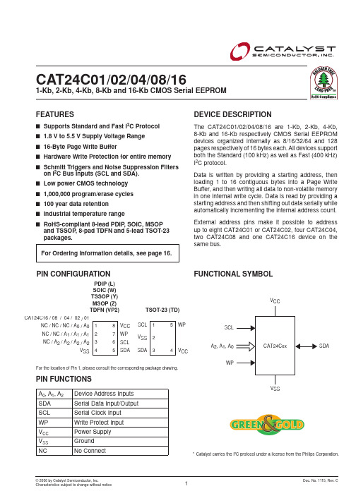
1© 2006 by Catalyst Semiconductor, Inc.Characteristics subject to change without noticeDoc. No. 1115, Rev. CCAT24C01/02/04/08/161-Kb, 2-Kb, 4-Kb, 8-Kb and 16-Kb CMOS Serial EEPROMPIN CONFIGURATIONFUNCTIONAL SYMBOLFEATURES■ Supports Standard and Fast I 2C Protocol ■ 1.8 V to 5.5 V Supply Voltage Range ■ 16-Byte Page Write Buffer■ Hardware Write Protection for entire memory ■ Schmitt Triggers and Noise Suppression Filterson I 2C Bus Inputs (SCL and SDA).■ Low power CMOS technology ■ 1,000,000 program/erase cycles ■ 100 year data retention ■ Industrial temperature range■ RoHS-compliant 8-lead PDIP , SOIC, MSOPand TSSOP , 8-pad TDFN and 5-lead TSOT-23 packages.PDIP (L)SOIC (W)TSSOP (Y)MSOP (Z)TDFN (VP2)V CCV SSSD ASCLWPA 2, A 1, A 0DEVICE DESCRIPTIONThe CAT24C01/02/04/08/16 are 1-Kb, 2-Kb, 4-Kb, 8-Kb and 16-Kb respectively CMOS Serial EEPROM devices organized internally as 8/16/32/64 and 128 pages respectively of 16 bytes each. All devices support both the Standard (100 kHz) as well as Fast (400 kHz) I 2C protocol.Data is written by providing a starting address, then loading 1 to 16 contiguous bytes into a Page Write Buffer, and then writing all data to non-volatile memory in one internal write cycle. Data is read by providing a starting address and then shifting out data serially while automatically incrementing the internal address count. External address pins make it possible to address up to eight CAT24C01 or CAT24C02, four CAT24C04, two CAT24C08 and one CAT24C16 device on the same bus.8765V CC WP SCL SDANC / A 2 / A 2 / A 2 / A 2NC / NC / NC / A 0 / A 0CAT24C16 / 08 / 04 / 02 / 01NC / NC / A 1 / A 1 / A 1V SS1234For the location of Pin 1, please consult the corresponding package drawing.PIN FUNCTIONSA 0, A 1, A2Device Address Inputs SDA Serial Data Input/Output SCL Serial Clock Input WP Write Protect Input V CC Power Supply V SS Ground NCNo Connect* Catalyst carries the I 2C protocol under a license from the Philips Corporation.TSOT-23 (TD)54WPV CC SCL V SS SDA123For Ordering Information details, see page 16.2Doc. No. 1115, Rev. C© 2006 by Catalyst Semiconductor, Inc.Characteristics subject to change without noticeABSOLUTE MAXIMUM RATINGS (1) Storage Temperature-65°C to +150°C Voltage on Any Pin with Respect to Ground (2) -0.5 V to +6.5 VRELIABILITY CHARACTERISTICS (3)Symbol Parameter Min UnitsN END (4)Endurance 1,000,000Program/ Erase CyclesT DRData Retention100YearsD.C. OPERATING CHARACTERISTICSV CC = 1.8 V to 5.5 V, T A = -40°C to 85°C, unless otherwise specified. Symbol Parameter Test Conditions MinMax Units I CCR Read Current Read, f SCL = 400 kHz 1mA I CCW Write Current Write, f SCL = 400 kHz 1mA I SB Standby Current All I/O Pins at GND or V CC 1μA I L I/O Pin Leakage Pin at GND or V CC1μA V IL Input Low Voltage -0.5V CC x 0.3V V IH Input High Voltage V CC x 0.7V CC + 0.5V V OL1Output Low Voltage V CC ≥ 2.5 V, I OL = 3.0 mA 0.4V V OL2Output Low VoltageV CC < 2.5 V, I OL = 1.0 mA 0.2VPIN IMPEDANCE CHARACTERISTICSV CC = 1.8 V to 5.5 V, T A = -40°C to 85°C, unless otherwise specified.Symbol ParameterConditions Max Units C IN (3)SDA I/O Pin Capacitance V IN = 0 V 8pF C IN (3)Input Capacitance (other pins)V IN = 0 V6pFI WP (5)WP Input CurrentV IN < V IH, V CC = 5.5 V 200μAV IN < V IH, V CC = 3.3 V 150V IN < V IH, V CC = 1.8 V 100V IN > V IH1Note:(1) Stresses above those listed under “Absolute Maximum Ratings” may cause permanent damage to the device. These are stress ratingsonly, and functional operation of the device at these or any other conditions outside of those listed in the operational sections of this speci-fication is not implied. Exposure to any absolute maximum rating for extended periods may affect device performance and reliability.(2) The DC input voltage on any pin should not be lower than -0.5 V or higher than V CC + 0.5 V. During transitions, the voltage on any pin mayundershoot to no less than -1.5 V or overshoot to no more than V CC + 1.5 V, for periods of less than 20 ns.(3) These parameters are tested initially and after a design or process change that affects the parameter according to appropriate AEC-Q100and JEDEC test methods.(4) Page Mode, V CC = 5 V, 25°C(5) When not driven, the WP pin is pulled down to GND internally. For improved noise immunity, the internal pull-down is relatively strong;therefore the external driver must be able to supply the pull-down current when attempting to drive the input HIGH. To conserve power, as the input level exceeds the trip point of the CMOS input buffer (~ 0.5 x V CC ), the strong pull-down reverts to a weak current source.CAT24C01/02/04/08/163Doc No. 1115, Rev. C© 2006 by Catalyst Semiconductor, Inc.Characteristics subject to change without noticeA.C. CHARACTERISTICS (1)V CC = 1.8 V to 5.5 V, T A = -40°C to 85°C.Symbol Parameter StandardFast Units Min Max Min Max F SCL Clock Frequency100400kHz t HD:STA START Condition Hold Time 40.6μs t LOW Low Period of SCL Clock 4.7 1.3μs t HIGH High Period of SCL Clock 40.6μs t SU:STA START Condition Setup Time 4.70.6μs t HD:DAT Data In Hold Time 00μs t SU:DAT Data In Setup Time 250100nst R SDA and SCL Rise Time 1000300ns t F (2)SDA and SCL Fall Time 300300ns t SU:STO STOP Condition Setup Time40.6μs t BUF Bus Free Time Between STOP and START 4.71.3μst AA SCL Low to Data Out Valid 3.50.9μs t DH Data Out Hold Time100100ns T i (2)Noise Pulse Filtered at SCL and SDA Inputs 100100ns t SU:WP WP Setup Time 00μs t HD:WP WP Hold Time 2.52.5μst WR Write Cycle Time 55ms t PU (2, 3)Power-up to Ready Mode11msNote:(1) Test conditions according to “A.C. Test Conditions” table.(2) Tested initially and after a design or process change that affects this parameter.(3) t PU is the delay between the time V CC is stable and the device is ready to accept commands.A.C. TEST CONDITIONS Input Levels0.2 x V CC to 0.8 x V CCInput Rise and Fall Times ≤ 50 nsInput Reference Levels 0.3 x V CC , 0.7 x V CC Output Reference Levels 0.5 x V CCOutput LoadCurrent Source: I OL = 3 mA (V CC ≥ 2.5 V); I OL = 1 mA (V CC < 2.5 V); C L = 100 pF4Doc. No. 1115, Rev. C© 2006 by Catalyst Semiconductor, Inc.Characteristics subject to change without noticePOWER-ON RESET (POR)Each CAT24Cxx* incorporates Power-On Reset (POR) circuitry which protects the internal logic against powering up in the wrong state.A CAT24Cxx device will power up into Standby mode after V CC exceeds the POR trigger level and will power down into Reset mode when V CC drops below the POR trigger level. This bi-directional POR feature protects the device against ‘brown-out’ failure following a temporary loss of power.* For common features, the CAT24C01/02/04/08/16 will be refered to as CAT24CxxPIN DESCRIPTIONSCL: The Serial Clock input pin accepts the Serial Clock generated by the Master.SDA: The Serial Data I/O pin receives input data and transmits data stored in EEPROM. In transmit mode, this pin is open drain. Data is acquired on the positive edge, and is delivered on the negative edge of SCL.A0, A1 and A2: The Address inputs set the device ad-dress when cascading multiple devices. When not driven, these pins are pulled LOW internally.WP: The Write Protect input pin inhibits all write opera-tions, when pulled HIGH. When not driven, this pin is pulled LOW internally.FUNCTIONAL DESCRIPTIONThe CAT24Cxx supports the Inter-Integrated Circuit (I 2C) Bus data transmission protocol, which defines a device that sends data to the bus as a transmitter and a device receiving data as a receiver. Data flow is controlled by a Master device, which generates the serial clock and all START and STOP conditions. The CAT24Cxx acts as a Slave device. Master and Slave alternate as either transmitter or receiver.I 2C BUS PROTOCOLThe I 2C bus consists of two ‘wires’, SCL and SDA. The two wires are connected to the V CC supply via pull-up resistors. Master and Slave devices connect to the 2-wire bus via their respective SCL and SDA pins. The transmitting device pulls down the SDA line to ‘transmit’ a ‘0’ and releases it to ‘transmit’ a ‘1’.Data transfer may be initiated only when the bus is not busy (see A.C. Characteristics).During data transfer, the SDA line must remain stable while the SCL line is HIGH. An SDA transition while SCL is HIGH will be interpreted as a START or STOP condition (Figure 1). The START condition precedes all commands. It consists of a HIGH to LOW transition on SDA while SCL is HIGH. The START acts as a ‘wake-up’ call to all receivers. Absent a START, a Slave will not respond to commands. The STOP condition completes all commands. It consists of a LOW to HIGH transition on SDA while SCL is HIGH.Device AddressingThe Master initiates data transfer by creating a START condition on the bus. The Master then broadcasts an 8-bit serial Slave address. For normal Read/Write opera-tions, the first 4 bits of the Slave address are fixed at 1010 (Ah). The next 3 bits are used as programmable address bits when cascading multiple devices and/or as internal address bits. The last bit of the slave address, R/W , specifies whether a Read (1) or Write (0) operation is to be performed. The 3 address space extension bits are assigned as illustrated in Figure 2. A 2, A 1 and A 0 must match the state of the external address pins, and a 10, a 9 and a 8 are internal address bits.AcknowledgeAfter processing the Slave address, the Slave responds with an acknowledge (ACK) by pulling down the SDA line during the 9th clock cycle (Figure 3). The Slave will also acknowledge the address byte and every data byte presented in Write mode. In Read mode the Slave shifts out a data byte, and then releases the SDA line during the 9th clock cycle. As long as the Master acknowledges the data, the Slave will continue transmitting. The Master terminates the session by not acknowledging the last data byte (NoACK) and by issuing a STOP condition. Bus timing is illustrated in Figure 4.CAT24C01/02/04/08/165Doc No. 1115, Rev. C© 2006 by Catalyst Semiconductor, Inc.Characteristics subject to change without noticeFigure 3. Acknowledge TimingFigure 2. Slave Address BitsFigure 4. Bus Timing6Doc. No. 1115, Rev. C© 2006 by Catalyst Semiconductor, Inc.Characteristics subject to change without noticeWRITE OPERATIONSByte WriteIn Byte Write mode, the Master sends the START condi-tion and the Slave address with the R/W bit set to zero to the Slave. After the Slave generates an acknowledge, the Master sends the byte address that is to be written into the address pointer of the CAT24Cxx. After receiv-ing another acknowledge from the Slave, the Master transmits the data byte to be written into the addressed memory location. The CAT24Cxx device will acknowl-edge the data byte and the Master generates the STOP condition, at which time the device begins its internal Write cycle to nonvolatile memory (Figure 5). While this internal cycle is in progress (t WR ), the SDA output will be tri-stated and the CAT24Cxx will not respond to any request from the Master device (Figure 6).Page WriteThe CAT24Cxx writes up to 16 bytes of data in a single write cycle, using the Page Write operation (Figure 7). The Page Write operation is initiated in the same manner as the Byte Write operation, however instead of termi-nating after the data byte is transmitted, the Master is allowed to send up to fifteen additional bytes. After each byte has been transmitted the CAT24Cxx will respond with an acknowledge and internally increments the four low order address bits. The high order bits that define the page address remain unchanged. If the Master transmits more than sixteen bytes prior to sending the STOP condition, the address counter ‘wraps around’ to the beginning of page and previously transmitted data will be overwritten. Once all sixteen bytes are received and the STOP condition has been sent by the Master, the internal Write cycle begins. At this point all received data is written to the CAT24Cxx in a single write cycle.Acknowledge PollingThe acknowledge (ACK) polling routine can be used to take advantage of the typical write cycle time. Once the stop condition is issued to indicate the end of the host’s write operation, the CAT24Cxx initiates the internal write cycle. The A CK polling can be initiated immediately. This involves issuing the start condition followed by the slave address for a write operation. If the CAT24Cxx is still busy with the write operation, NoACK will be returned. If the CAT24Cxx has completed the internal write operation, an ACK will be returned and the host can then proceed with the next read or write operation.Hardware Write ProtectionWith the WP pin held HIGH, the entire memory is protected against Write operations. If the WP pin is left floating or is grounded, it has no impact on the operation of the CAT24Cxx. The state of the WP pin is strobed on the last falling edge of SCL immediately preceding the first data byte (Figure 8). If the WP pin is HIGH during the strobe interval, the CAT24Cxx will not acknowledge the data byte and the Write request will be rejected.Delivery StateThe CAT24Cxx is shipped erased, i.e., all bytes are FFh.CAT24C01/02/04/08/167Doc No. 1115, Rev. C© 2006 by Catalyst Semiconductor, Inc.Characteristics subject to change without noticeFigure 7. Page Write SequenceFigure 6. Write Cycle TimingFigure 5. Byte Write SequenceFigure 8. WP TimingADDRESS BYTEDATA BYTESCLSDAWP8Doc. No. 1115, Rev. C© 2006 by Catalyst Semiconductor, Inc.Characteristics subject to change without noticeREAD OPERATIONSImmediate ReadUpon receiving a Slave address with the R/W bit set to ‘1’, the CAT24Cxx will interpret this as a request for data residing at the current byte address in memory. The CAT24Cxx will acknowledge the Slave address, will immediately shift out the data residing at the current address, and will then wait for the Master to respond. If the Master does not acknowledge the data (NoACK) and then follows up with a STOP condition (Figure 9), the CAT24Cxx returns to Standby mode.Selective ReadSelective Read operations allow the Master device to select at random any memory location for a read opera-tion. The Master device first performs a ‘dummy’ write operation by sending the START condition, slave ad-dress and byte address of the location it wishes to read. After the CAT24Cxx acknowledges the byte address, the Master device resends the START condition and the slave address, this time with the R/W bit set to one. The CAT24Cxx then responds with its acknowledge and sends the requested data byte. The Master device does not acknowledge the data (NoACK) but will generate a STOP condition (Figure 10).Sequential ReadIf during a Read session, the Master acknowledges the 1st data byte, then the CAT24Cxx will continue transmitting data residing at subsequent locations until the Master responds with a NoACK, followed by a STOP (Figure 11). In contrast to Page Write, during Sequential Read the address count will automatically increment to and then wrap-around at end of memory (rather than end of page). In the CAT24C01, the internal address count will not wrap around at the end of the 128 byte memory space.CAT24C01/02/04/08/169Doc No. 1115, Rev. C© 2006 by Catalyst Semiconductor, Inc.Characteristics subject to change without noticeFigure 11. Sequential Read SequenceFigure 10. Selective Read SequenceFigure 9. Immediate Read Sequence and Timing10Doc. No. 1115, Rev. C© 2006 by Catalyst Semiconductor, Inc.Characteristics subject to change without noticePACKAGE OUTLINE8-lead 300 MIL Wide Plastic DIP (L)e24C16_8-LEAD_DIP_(300P).epsSYMBOLA A1b b2D E E1e eB LMIN 0.380.369.027.626.09 6.357.870.1150.1300.150NOM 0.461.771.147.872.54 BSC MAX 4.57A23.05 3.810.5610.168.257.119.65Notes:(1) All dimensions are in millimeters. Angels in degrees.(2) Complies with JEDEC Standard MS001.(3) Dimensioning and tolerancing per ANSI Y14.5M-1982CAT24C01/02/04/08/1611Doc No. 1115, Rev. C© 2006 by Catalyst Semiconductor, Inc.Characteristics subject to change without notice8-lead 150 Mil Wide Soic (W)24C16_8-LEAD_SOIC.epsSYMBOLA1A b C D E E1h L MIN 0.101.350.334.805.803.800.250.40NOM 0.250.19MAX 0.251.750.515.006.204.00e 1.27 BSC0.501.27θ10°8°eNotes:(1) All dimensions are in millimeters. Angels in degrees.(2) Complies with JEDEC specification MS-012 dimensions.For current Tape and Reel information, download the PDF file from: /documents/tapeandreel.pdf.12Doc. No. 1115, Rev. C© 2006 by Catalyst Semiconductor, Inc.Characteristics subject to change without notice8-Lead TSSOP (Y)θ1SEE DETAIL AcSYMBOLA A1A2b c D E E1e L θ1MIN 0.050.800.092.906.30 6.44.300.008.00NOM 0.900.300.19 3.004.400.600.750.50MAX 1.200.151.050.203.106.504.500.65 BSC Notes:(1) All dimensions are in millimeters. Angels in degrees.(2) Complies with JEDEC specification MO-153.For current Tape and Reel information, download the PDF file from: /documents/tapeandreel.pdf.CAT24C01/02/04/08/1613Doc No. 1115, Rev. C© 2006 by Catalyst Semiconductor, Inc.Characteristics subject to change without notice8-Lead MSOP (Z)Notes:(1) All dimensions are in millimeters. Angels in degrees.(2) Complies with JEDEC specification MS-187.(3) Stand off height/coplanarity are considered as special characteristics.14Doc. No. 1115, Rev. C© 2006 by Catalyst Semiconductor, Inc.Characteristics subject to change without notice8-PAD TDFN 2X3 PACKAGE (VP2)Notes:(1) All dimensions are in millimeters. Angels in degrees.(2) Complies with JEDEC specification MO-229.CAT24C01/02/04/08/1615Doc No. 1115, Rev. C© 2006 by Catalyst Semiconductor, Inc.Characteristics subject to change without notice5-Lead TSOT-23 (TD)5 LEAD TSOT-23 PACKAGEMAX 1.00.10.90.450.200.508°NOM —0.050.87—0.152.90 BSC 2.80 BSC 1.60 BSC 1.90 BSC 0.400.25 BSCMIN —0.010.800.300.120.300°SYMBOLA A1A2b c D E E10.95 BSC e e1L 0.60 REF L1L2θNotes:(1) All dimensions are in millimeters. Angels in degrees.(2) Complies with JEDEC specification MO-193.For current Tape and Reel information, download the PDF file from: /documents/tapeandreel.pdf.16Doc. No. 1115, Rev. C© 2006 by Catalyst Semiconductor, Inc.Characteristics subject to change without noticeEXAMPLE OF ORDERING INFORMATION(1) All packages are RoHS-compliant (Lead-free, Halogen-free).(2) The standard lead finish is NiPdAu pre-plated (PPF) lead frames.(3) The device used in the above example is a CAT24C16YI-GT3 (TSSOP , Industrial Temperature, NiPdAu, Tape & Reel).(4) For availability, please contact your nearest Catalyst Semiconductor Sales Office.(5) For additional package and temperature options, please contact your nearest Catalyst Semiconductor Sales office.Catalyst Semiconductor, Inc.Corporate Headquarters 2975 Stender Way Santa Clara, CA 95054Phone: 408.542.1000Fax: Publication #: 1115Revison: C Issue date: 11/29/06Copyrights, Trademarks and PatentsTrademarks and registered trademarks of Catalyst Semiconductor include each of the following: AE 2 ™,Beyond Memory ™,DPP ™,EZDim ™,MiniPot™ andQuad-Mode ™Catalyst Semiconductor has been issued U.S. and foreign patents and has patent applications pending that protect its products.CATALYST SEMICONDUCTOR MAKES NO WARRANTY, REPRESENTATION OR GUARANTEE, EXPRESS OR IMPLIED, REGARDING THE SUITABILITY OF ITS PRODUCTS FOR ANY PARTICULAR PURPOSE, NOR THAT THE USE OF ITS PRODUCTS WILL NOT INFRINGE ITS INTELLECTUAL PROPERTY RIGHTS OR THE RIGHTS OF THIRD PARTIES WITH RESPECT TO ANY PARTICULAR USE OR APPLICATION AND SPECIFICALLY DISCLAIMS ANY AND ALL LIABILITY ARISING OUT OF ANY SUCH USE OR APPLICATION, INCLUDING BUT NOT LIMITED TO, CONSEQUENTIAL OR INCIDENTAL DAMAGES.Catalyst Semiconductor products are not designed, intended, or authorized for use as components in systems intended for surgical implant into the body, or other applications intended to support or sustain life, or for any other application in which the failure of the Catalyst Semiconductor product could create a situation where personal injury or death may occur.Catalyst Semiconductor reserves the right to make changes to or discontinue any product or service described herein without notice. Products with data sheets labeled “Advance Information” or “Preliminary” and other products described herein may not be in production or offered for sale.Catalyst Semiconductor advises customers to obtain the current version of the relevant product information before placing orders. Circuit diagrams illustrate typical semiconductor applications and may not be complete.REVISION HISTORYDate Revision Comments07/18/06A Combine 5 data sheets into one data sheet.07/31/06B Update Package Marking11/29/06CUpdate FeaturesUpdate Pin Configuration Update Functional SymbolAdded 8-Lead MSOP Package Outline Remove Package MarkingUpdate Example of Ordering Information。
CAT24C641中文资料
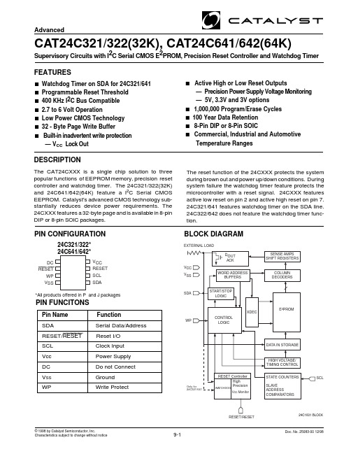
© 1998 by Catalyst Semiconductor, Inc. Characteristics subject to change without noticeDoc. No. 25083-00 12/989-1CAT24C321/322/641/6422AdvancedDoc. No. 25083-00 12/98ABSOLUTE MAXIMUM RATINGS*Temperature Under Bias....................–55°C to +125°C Storage Temperature........................ –65°C to +150°C Voltage on Any Pin withRespect to Ground (1) ..............–2.0V to +V CC + 2.0V V CC with Respect to Ground..................–2.0V to +7.0V Package Power DissipationCapability (Ta = 25°C)1.0W.................................1.0W Lead Soldering Temperature (10 secs)...............300°C Output Short Circuit Current (2) ..........................100mACOMMENTStresses above those listed under “Absolute Maximum Ratings” may cause permanent damage to the device.These are stress ratings only, and functional operation of the device at these or any other conditions outside of those listed in the operational sections of this specifica-tion is not implied. Exposure to any absolute maximum rating for extended periods may affect device perfor-mance and reliability.RELIABILITY CHARACTERISTICSSymbol Parameter Min.Max. Units Reference Test MethodN END (3)Endurance 1,000,000 Cycles/Byte MIL-STD-883, Test Method 1033 T DR (3)Data Retention 100 Years MIL-STD-883, Test Method 1008 V ZAP (3)ESD Susceptibility 2000 Volts MIL-STD-883, Test Method 3015 I LTH (3)(4)Latch-up 100 mAJEDEC Standard 17D.C. OPERATING CHARACTERISTICSV CC = +2.7V to +6.0V, unless otherwise specified.Symbol Parameter Min. Typ. Max. Units Test Conditions I CC Power Supply Current 3mA f SCL = 100 KHzIsbStandby Current40 µAVcc=3.3V50 µA Vcc=5I LI Input Leakage Current 2 µA V IN =G ND or V CC I LO Output Leakage Current10µA V IN =G ND or V CCV IL Input Low Voltage –1 V CC x 0.3 V V IH Input High Voltage V CC x 0.7 V CC + 0.5 VV OLOutput Low Voltage (SDA)0.4 V I OL = 3 mA ,V CC =3.0VLimitsCAPACITANCE T A = 25°C, f = 1.0 MHz, V CC = 5V Symbol Test Max.Units Conditions C I/O (3) Input/Output Capacitance (SDA)8pF V I/O = 0V C IN (3)Input Capacitance (SCL)6pFV IN = 0VNote:(1)The minimum DC input voltage is –0.5V. During transitions, inputs may undershoot to –2.0V for periods of less than 20 ns. Maximum DCvoltage on output pins is V CC +0.5V, which may overshoot to V CC + 2.0V for periods of less than 20ns.(2)Output shorted for no more than one second. No more than one output shorted at a time.(3)This parameter is tested initially and after a design or process change that affects the parameter.(4)Latch-up protection is provided for stresses up to 100 mA on address and data pins from –1V to V CC +1V.CAT24C321/322/641/6423AdvancedDoc. No. 25083-00 12/98A.C. CHARACTERISTICSV CC =2.7V to 6.0V unless otherwise specified.Output Load is 1 TTL Gate and 100pFRead & Write Cycle Limits SymbolParameterV CC =2.7V - 6V V CC =4.5V - 5.5V Min.Max.Min.Max.Units F SCL Clock Frequency100400kHz T I (1)Noise Suppression Time200200ns Constant at SCL, SDA Inputs t AA SCL Low to SDA Data Out 3.51µs and ACK Outt BUF (1)Time the Bus Must be Free Before 4.7 1.2µs a New Transmission Can Start t HD:STA Start Condition Hold Time 40.6µs t LOW Clock Low Period 4.7 1.2µs t HIGH Clock High Period40.6µs t SU:STA Start Condition Setup Time4.70.6µs (for a Repeated Start Condition)t HD:DAT Data In Hold Time 00ns t SU:DAT Data In Setup Time 5050ns t R (1)SDA and SCL Rise Time 10.3µs t F (1)SDA and SCL Fall Time 300300ns t SU:STO Stop Condition Setup Time 40.6µs t DHData Out Hold Time100100nsPower-Up Timing (1)(2)Symbol ParameterMax.Units t PUR Power-up to Read Operation 1ms t PUWPower-up to Write Operation1msNote:(1)This parameter is tested initially and after a design or process change that affects the parameter.(2)t PUR and t PUW are the delays required from the time V CC is stable until the specified operation can be initiated.Write Cycle Limits Symbol Parameter Min.Typ.Max Units t WRWrite Cycle Time10msThe write cycle time is the time from a valid stop condition of a write sequence to the end of the internal program/erase cycle. During the write cycle, the bus interface circuits are disabled, SDA is allowed to remain high, and the device does not respond to its slave address.CAT24C321/322/641/6424AdvancedDoc. No. 25083-00 12/98RESET CIRCUIT CHARACTERISTICSCAT24C321/322/641/6425AdvancedDoc. No. 25083-00 12/98PIN DESCRIPTIONSWP : WRITE PROTECTIf the pin is tied to V CC the entire memory array becomes Write Protected (READ only). When the pin is tied to V SS or left floating normal read/write operations are allowed to the device.SCL : SERIAL CLOCKThe serial clock input clocks all data transferred into or out of the device.RESET/RESET : RESET I/OThese are open drain pins and can be used as reset trigger inputs. By forcing a reset condition on the pins the device will initiate and maintain a reset condition for approximately 200ms. RESET pin must be connected through a pull-down and RESET pin must be connected through a pull-up device.SDA: SERIAL DATA/ADDRESSThe bidirectional serial data/address pin is used to transfer all data into and out of the device. The SDA pin is an open drain output and can be wire-ORed with other open drain or open collector outputs. In the 24C321/641, the SDA line is also used as the Watchdog Timer Monitor.Reset Controller DescriptionThe CAT24CXXX provides a precision RESET control-ler that ensures correct system operation during brown-out and power-up/down conditions. It is configured with open drain RESET outputs. During power-up, the RESET outputs remain active until V CC reaches the V TH threshold and will continue driving the outputs for approximately 200ms (t PURST ) after reaching V TH. After the t PURST timeout interval, the device will cease to drive reset outputs. At this point the reset outputs will be pulled up or down by their respective pull up/pull down devices. During power-down, the RESET outputs will begin driving active when V CC falls below V TH. The RESET outputs will be valid so long as V CC is >1.0V (V RVALID ).The RESET pins are I/Os; therefore, the CAT24CXXX can act as a signal conditioning circuit for an externally applied reset. The inputs are level triggered; that is, the RESET input in the 24CXXX will initiate a reset timeout after detecting a high and the RESET input in the 24CXXX will initiate a reset timeout after detecting a low.Watchdog TimerThe Watchdog Timer provides an independent protec-tion for microcontrollers. During a system failure, the CAT24C321/641 will respond with a reset signal after a time-out interval of 1.6 seconds for lack of activity.24CXX1 is designed with the Watchdog Timer feature on the SDA input. For the 24C321/641, if the microcontroller does not toggle the SDA input pin within 1.6 seconds the Watchdog Timer times out. This will generate a reset condition on reset outputs. The Watch-dog Timer is cleared by any transition on SDA.As long as the reset signal is asserted, the Watchdog Timer will not count and will stay cleared. 24C322/642does not feature the Watchdog Timer function.DEVICE OPERATIONV CCV RESETCAT24C321/322/641/6426AdvancedDoc. No. 25083-00 12/98Hardware Data ProtectionThe 24CXXX is designed with the following hardware data protection features to provide a high degree of data integrity.(1) The 24CXXX features a WP pin. When WP pin is tied high the entire memory array becomes write protected (read only).(2) The V CC sense provides write protection when V CC falls below the reset threshold value (V TH ). The V CC lock out inhibits writes to the serial EEPROM whenever V CC falls below (power down) V TH or until V CC reaches the reset threshold (power up) V TH .Reset Threshold VoltageFrom the factory the 24CXXX is offered in five different variations of reset threshold voltages. They are 4.50-4.75V, 4.25-4.50V, 3.00-3.15V, 2.85-3.00V and 2.55-2.70V. To provide added flexibility to design engineers using this product, the 24CXXX is designed with an additional feature of programming the reset threshold voltage. This allows the user to change the existing reset threshold voltage to one of the other four reset threshold voltages. Once the reset threshold voltage is selected it will not change even after cycling the power,unless the user uses the programmer to change the reset threshold voltage. However, the programming function is available only through third party programmer manufacturers. Please call Catalyst for a list of program-mer manufacturers who support this function.STOPCONDITIONSTARTCONDITIONADDRESSSCLSDAFigure 3. Write Cycle TimingSTART BITSDASTOP BITSCLFigure 4. Start/Stop TimingSCLSDA INSDA OUTFigure 2. Bus TimingCAT24C321/322/641/6427AdvancedDoc. No. 25083-00 12/98ACKNOWLEDGESTARTSCL FROM MASTERDATA OUTPUTFROM TRANSMITTERDATA OUTPUT FROM RECEIVERFigure 5. Acknowledge TimingFigure 6. Slave Address BitsFUNCTIONAL DESCRIPTIONThe CAT24CXXX supports the I 2C Bus data transmis-sion protocol. This Inter-Integrated Circuit Bus protocol defines any device that sends data to the bus to be a transmitter and any device receiving data to be a re-ceiver. The transfer is controlled by the Master device which generates the serial clock and all START and STOP conditions for bus access. The CAT24CXXX operates as a Slave device. Both the Master device and Slave device can operate as either transmitter or re-ceiver, but the Master device controls which mode is activated.I 2C BUS PROTOCOLThe features of the I 2C bus protocol are defined as follows:(1) Data transfer may be initiated only when the bus is not busy.(2) During a data transfer, the data line must remain stable whenever the clock line is high. Any changes in the data line while the clock line is high will be interpreted as a START or STOP condition.START ConditionThe START Condition precedes all commands to the device, and is defined as a HIGH to LOW transition of SDA when SCL is HIGH. The CAT24CXXX monitors the SDA and SCL lines and will not respond until this condition is met.STOP ConditionA LOW to HIGH transition of SDA when SCL is HIGH determines the STOP condition. All operations must end with a STOP condition.DEVICE ADDRESSINGThe Master begins a transmission by sending a START condition. The Master sends the address of the particu-lar slave device it is requesting. The four most significant bits of the 8-bit slave address are fixed as 1010.The next three bits are don't care. The last bit of the slave address specifies whether a Read or Write operation is to be performed. When this bit is set to 1, a Read operation is selected, and when set to 0, a Write opera-tion is selected.After the Master sends a START condition and the slave address byte, the CAT24CXXX monitors the bus and responds with an acknowledge (on the SDA line) when its address matches the transmitted slave address. The CAT24CXXX then performs a Read or Write operation depending on the state of the R/W bit.1010X R/WX XCAT24C321/322/641/6428AdvancedDoc. No. 25083-00 12/98Figure 7. Byte Write TimingFigure 8. Page Write TimingACKNOWLEDGEAfter a successful data transfer, each receiving device is required to generate an acknowledge. The Acknowledg-ing device pulls down the SDA line during the ninth clock cycle, signaling that it received the 8 bits of data.The CAT24CXXX responds with an acknowledge after receiving a START condition and its slave address. If the device has been selected along with a write operation,it responds with an acknowledge after receiving each 8-bit byte.When the CAT24CXXX begins a READ mode it trans-mits 8 bits of data, releases the SDA line, and monitors the line for an acknowledge. Once it receives this ac-knowledge, the CAT24CXXX will continue to transmit data. If no acknowledge is sent by the Master, the device terminates data transmission and waits for a STOP condition.WRITE OPERATIONSByte WriteIn the Byte Write mode, the Master device sends the START condition and the slave address information (with the R/W bit set to zero) to the Slave device. After t he Slave generates an acknowledge, the Master sends a 8-bit address that is to be written into the address pointers of the CAT24CXXX. After receiving another acknowledge from the Slave, the Master device trans-mits the data to be written into the addressed memory location. The CAT24CXXX acknowledges once more and the Master generates the STOP condition. At this time, the device begins an internal programming cycle to nonvolatile memory. While the cycle is in progress, the device will not respond to any request from the Master device.Page WriteThe 24CXXX writes up to 32 bytes of data in a single write cycle, using the Page Write operation. The page write operation is initiated in the same manner as the byte write operation, however instead of terminating after the initial byte is transmitted, the Master is allowed to send up to 31 additional bytes. After each byte has been transmitted, CAT24CXXX will respond with an acknowledge, and internally increment the lower order address bits by one. The high order bits remain un-changed.If the Master transmits more than 32 bytes before sending the STOP condition, the address counter ‘wraps around’, and previously transmitted data will be overwrit-ten.When all 32 bytes are received, and the STOP condi tion has been sent by the Master, the internal program-ming cycle begins. At this point, all received data is written to the CAT24CXXX in a single write cycle.* = Don't care bit for 24C321/322X= Don't care bitA 15–A 8SLAVE ADDRESSSA C KAC KDATAA C KS T O P P BUS ACTIVITY:MASTERSDA LINES T A R T A 7–A 0BYTE ADDRESS A C K*X X XSLAVE C KC KC KBUS ACTIVITY:MASTERSDA LINES T A BYTE ADDRESS C KS T C K C KC KCAT24C321/322/641/6429AdvancedDoc. No. 25083-00 12/98Figure 9. Immediate Address Read TimingAcknowledge PollingDisabling of the inputs can be used to take advantage of the typical write cycle time. Once the stop condition is issued to indicate the end of the host’s write operation,CAT24CXXX initiates the internal write cycle. ACK poll-ing can be initiated immediately. This involves issuing the start condition followed by the slave address for a write operation. If CAT24CXXX is still busy with the write operation, no ACK will be returned. If CAT24CXXX has completed the write operation, an ACK will be returned and the host can then proceed with the next read or write operation.WRITE PROTECTIONThe Write Protection feature allows the user to protect against inadvertent programming of the memory array.If the WP pin is tied to V CC , the entire memory array is protected and becomes read only. The CAT24CXXX will accept both slave and byte addresses, but the memory location accessed is protected from program-ming by the device's failure to send an acknowledge after the first byte of data is received.READ OPERATIONSThe READ operation for the CAT24CXXX is initiated in the same manner as the write operation with one excep-tion, that R/W bit is set to one. Three different READ operations are possible: Immediate/Current Address READ, Selective/Random READ and Sequential READ.SCL SDA 8TH BIT STOPNO ACKDATA OUT89SLAVE ADDRESSSA C KBUS ACTIVITY:MASTERSDA LINES T A R T N O A C KDATAS T O P PCAT24C321/322/641/64210AdvancedDoc. No. 25083-00 12/98Figure 10. Selective Read TimingFigure 11. Sequential Read TimingImmediate/Current Address ReadThe CAT24CXXX’s address counter contains the ad-dress of the last byte accessed, incremented by one. In other words, if the last READ or WRITE access was to address N, the READ immediately following would ac-cess data from address N+1. If N=E (where E=4095 for 24C321/322 and E=8191 for 24C641/642), then the counter will ‘wrap around’ to address 0 and continue to clock out data. After the CAT24CXXX receives its slave address information (with the R/W bit set to one), it issues an acknowledge, then transmits the 8-bit byte requested. The master device does not send an ac-knowledge, but will generate a STOP condition.Selective/Random ReadSelective/Random READ operations allow the Master device to select at random any memory location for a READ operation. The Master device first performs a ‘dummy’ write operation by sending the START condi-tion, slave address and byte addresses of the location it wishes to read. After CAT24CXXX acknowledges, the Master device sends the START condition and the slave address again, this time with the R/W bit set to one.The CAT24CXXX then responds with its acknowledge and sends the 8-bit byte requested. The master deviceSequential ReadThe Sequential READ operation can be initiated by either the Immediate Address READ or Selective READ operations. After the CAT24CXXX sends the initial 8-bit byte requested, the Master will respond with an acknowledge which tells the device it requires more data. The CAT24CXXX will continue to output an 8-bit byte for each acknowledge sent by the Master. The operation will terminate when the Master fails to respond with an acknowledge, thus sending the STOP condition.The data being transmitted from CAT24CXXX is output-ted sequentially with data from address N followed by data from address N+1. The READ operation address counter increments all of the CAT24CXXX address bits so that the entire memory array can be read during one operation. If more than E (where E= 4095 for 24C321/322, E=511 and E=8191 for 24C641/642) bytes are read out, the counter will ‘wrap around’ and continue to clock out data bytes.does not send an acknowledge but will generate a STOP condition.BUS ACTIVITY:MASTERSDA LINEDATA n+xDATA nC KC KDATA n+1C KS T O O A C KDATA n+2C KSLAVE ADDRESS* = Don't care bit for 24C321/322X= Don't care bitA 15–A 8SLAVE ADDRESSSA C KA C KA C KBUS ACTIVITY:MASTERSDA LINES T A R T A 7–A 0BYTE ADDRESS SLAVEADDRESSSA C KN O A C KS T A R T DATAPS T O P X X X *CAT24C321/322/641/64211Advanced Doc. No. 25083-00 12/98Ordering InformationNote:(1) The device used in the above example is a CAT24C322JI-30TE13 (32K I 2C Memory, SOIC, Industrial Temperature, 3.0-3.15V ResetThreshold Voltage, Tape and Reel)CAT24C321/322/641/64212AdvancedDoc. No. 25083-00 12/98。
AT24C1024 中文说明书

AT24C10242线串行EEPROM特性低电压操作:2.7(Vcc=2.7V to 5.5V)内部组织:131,072*8位=1M2线串行接口施密特触发器,噪声抑制滤波输入双向数据传输协议时钟速率:400kHz(2.7V)和1MHz(5V)硬件写保护引脚和软件数据保护256字节页写模式(允许部分页面写入)随机和顺序读写模式自定义写周期(5ms)高可靠性:耐久力:写周期/页100,000次数据保留:40年8引脚PDIP,8引脚有铅SOIC封装,8引脚无铅阵列和8引脚球状dBGA封装描述AT24C1024提供1,048,567位的串行可电擦除和可编程只读存储器(EEPROM),它的每8位组成一个字节,共131,072个字节。
该设备的级联功能允许多达2个设备共亨同一条2-线总线。
该设备适合用于许多工业和商业,应用必要的低功耗和低电压的操作。
该器件可提供节省空间的8引脚PDIP,8引脚有铅SOIC封装,8引脚无铅阵列和8引脚球状dBGA封装。
另外,这一系列产品允许在2.7V(2.7V~5.5V)下工作。
绝对最大额定值:工作温度:-55~+125存储温度:-65~+150任何引脚的对地电压:-1.0V~+7.0V最大工作电压:6.25V直流输出电流:5.0mA注意:强制高出“绝对最大额定值”可能导致设备的永久损坏。
设备的压力等级和功能操作只有在这些或超出本规范所标明的其他任何条件下是不允许的。
长时间工作在绝对最大额定值的条件下可能影响设备的可靠性。
引脚描述::引脚描述串行时钟(SCL):SCL的输入是在时钟的上升沿数据进入每个EEPROM设备和下降沿数据输出每个设备。
串行数据(SDA):SDA引脚是双向串行数据传输的。
这个引脚是漏极输出的,可以与其它的漏极开路或集电极开路的设备线或。
器件/页地址(A1):A1引脚是设备的输入地址,它能够通过导线与不兼容的设备AT24C128/256/512连接。
当A1通过硬件连接时,2个以上的1024K设备可以在同一条系统总路线上寻址(下面会详细谈论设备的地址选择)。
中文数据手册AT24C系列

020 38730976 38730977 Fax 38730925
直流操作特性
Vcc=+1.8V +6.0V 除非特别说明
符号
参数
最小
ICC ISB ILI ILO VIL VIH VOL1 VOL2
电源电流 备用电流(Vcc=5.0V) 输入漏电流 输出漏电流 输入低电压 输入高电压 输出低电压 输出低电压
广州周立功单片机发展有限公司 Tel
020 38730976 38730977 Fax 38730925
目录
1 CSI24WC0 1/02/04/08/16 ……………………………….2-10 2 CSI24WC32/64…………………………………………...11-18 3 CSI24WC128. ……………………………..…………….19-26 4 CSI24WC256. ………………………….….…………….27-34
符号
测试项
CI/O
I/O 电容 SDA 脚
CIN
输出电容 A0 A1 A2 SCL WP
最大 8 6
单位 PF PF
条件 VI/O=0V VIN=0V
交流特性 Vcc=+1.8V +6.0V 除非特别说明 输出负载能力为 1 个 TTL 门和 100pF
读写周期范围
符号
参数
FSCL TI tAA tBUF tHD: STA tLOW tHIGH tSU: STA tHD: DAT tSUl: DAT tR tF tSU: STO tDH
1 Vcc 0.7
典型
最大 3 0 10 10
Vcc 0.3 Vcc+0.5
0.4 0.5
安特尔AT24C32D 32K Serial EEPROM数据手册说明书
AT24C32DI2C-Compatible (2-Wire) Serial EEPROM32-Kbit (4,096 x 8)DATASHEET Features●Low-voltage and Standard-voltage OperationV CC = 1.7V to 5.5V●Internally Organized as 4,096 x 8 (32K)●I2C-compatible (2-Wire) Serial Interface●Schmitt Trigger, Filtered Inputs for Noise Suppression●Bidirectional Data Transfer Protocol●400kHz (1.7V) and 1MHz (2.5V, 2.7V, 5.0V) Compatibility●Write Protect Pin for Hardware Protection●32-byte Page Write ModePartial Page Writes Allowed●Self-timed Write cycle (5ms Max)●High ReliabilityEndurance: 1,000,000 Write CyclesData Retention: 100 Years●Lead-free/Halogen-free devices Available●Green Package Options (Pb/Halide-free/RoHS Compliant)8-lead JEDEC SOIC, 8-lead TSSOP, 8-pad UDFN, 8-pad XDFN, 5-leadSOT23, 5-ball WLCSP, and 8-ball VFBGA packages●Die Sale Options: Wafer Form, Waffle Pack, and Bumped Wafers DescriptionThe Atmel® AT24C32D provides 32,768 bits of Serial Electrically Erasable and Programmable Read-Only Memory (EEPROM) organized as 4,096 words of 8 bits each. The device’s cascading feature allows up to eight devices to share a common 2-wire bus. The device is optimized for use in many industrial and commercial applications where low-power and low-voltage operation are essential. The devices are available in space-saving 8-lead JEDEC SOIC, 8-lead TSSOP, 8-pad UDFN, 8-pad XDFN, 5-lead SOT23, 5-ball WLCSP, and 8-ball VFBGA packages. In addition, this device operates from 1.7V to 5.5V.AT24C32D [DATASHEET]Atmel-8866D-SEEPROM-AT24C32D-Datasheet_12201621.Pin Configurations and PinoutsTable 1-1.Pin Configuration Note:When using the 5-lead SOT-23 or the 5-ball WLCSP , the software bits A2, A1, and A0 must be set to Logic 0 to properly communicate with the device.2.Absolute Maximum Ratings*8-pad UDFN/XDFNV CC WP SCL SDAA 0A 1A 2GND123487658-ball VFBGABottom View8-lead SOIC8-lead TSSOPTop View12348765A 0A 1A 2GNDV CC WP SCL SDATop View Top ViewA 0A 1A 2GND V CC WP SCL SDA87651234SCL GND SDA123545-lead SOT23WPV CC* Note: Drawings are not to scale5-ball WLCSPBall Side View(1)A 0A 1A 2GNDV CC WP SCL SDA12348765(1)Operating Temperature . . . . . . . . . . .-55°C to +125°C Storage Temperature . . . . . . . . . . . . -65°C to + 150°C Voltage on any pinwith respect to ground . . . . . . . . . . . . . . .-1.0 V +7.0V Maximum Operating Voltage . . . . . . . . . . . . . . . 6.25V DC Output Current. . . . . . . . . . . . . . . . . . . . . . .5.0mA*Notice:Stresses beyond those listed under “AbsoluteMaximum Ratings” may cause permanent damage to the device. This is a stress rating only and functional operation of the device at these or any other conditions beyond those indicated in the operational sections of this specification are not implied. Exposure to absolute maximum rating conditions forextended periods may affect device reliability.3AT24C32D [DATASHEET]Atmel-8866D-SEEPROM-AT24C32D-Datasheet_1220163.Block Diagram4.Pin DescriptionsSerial Clock (SCL): The SCL input is used to positive-edge clock data into each EEPROM device and negative-edge clock data out of each device.Serial Data (SDA): The SDA pin is bidirectional for serial data transfer. This pin is open drain driven and may be wire-ORed with any number of other open-drain or open-collector devices.Device Addresses (A 2, A 1, A 0): The A 2, A 1, and A 0 pins are device address inputs that are hard wired (directly to GND or to V CC ) for compatibility with other Atmel AT24C devices. When the pins are hard wired, as many as eight 32K devices may be addressed on a single bus system. (Device addressing is discussed in detail in Section 7., “Device Addressing” on page 9). A device is selected when a corresponding hardware and software match is true. If these pins are left floating, the A 2, A 1, and A 0 pins will be internally pulled down to GND. However, due to capacitive coupling that may appear during customer applications, Atmel recommends always connecting the address pins to a known state. When using a pull-up resistor, Atmel recommends using 10k Ω or less.Write Protect (WP): The Write Protect input, when connected to GND, allows normal write operations. When WP is connected directly to V CC , all Write operations to the memory are inhibited. If the pin is left floating, the WP pin will be internally pulled down to GND; however, due to capacitive coupling that may appear during customerapplications, Atmel recommends always connecting the WP pins to a known state. When using a pull-up resistor, Atmel recommends using 10k Ω or less.Table 4-1.Write ProtectV CC GND WP SCL SDAA 2A 1A 0AT24C32D [DATASHEET]Atmel-8866D-SEEPROM-AT24C32D-Datasheet_12201645.Memory OrganizationAT24C32D, 32K Serial EEPROM : The 32K is internally organized as 128 pages of 32-bytes each. Random word addressing requires a 12-bit data word address.5.1Pin CapacitanceTable 5-1.Pin Capacitance (1)Note:1.This parameter is characterized and is not 100% tested.5.2DC CharacteristicsTable 5-2.DC CharacteristicsNote:1.V IL min and V IH max are reference only and are not tested.Applicable over recommended operating range from: T A = 25°C, f = 1.0MHz, V CC = 5.5V.Applicable over recommended operating range from: T AI = -40°C to +85°C, V CC = 1.7V to 5.5V (unless otherwise noted).5AT24C32D [DATASHEET]Atmel-8866D-SEEPROM-AT24C32D-Datasheet_1220165.3AC CharacteristicsTable 5-3.AC Characteristics (Industrial Temperature)Notes:1.This parameter is ensured by characterization and is not 100% tested.2.AC measurement conditions:●R L (connects to V CC ): 1.3k Ω (2.5V, 5.5V), 10k Ω (1.7V)●Input pulse voltages: 0.3V CC to 0.7V CC ●Input rise and fall times: ≤ 50ns ●Input and output timing reference voltages: 0.5 x V CCApplicable over recommended operating range from: T AI = -40°C to +85°C, V CC = 1.7V to 5.5V, CL = 100pF (unless otherwise noted). Test conditions are listed in Note 2.AT24C32D [DATASHEET]Atmel-8866D-SEEPROM-AT24C32D-Datasheet_12201666.Device OperationClock and Data Transitions: The SDA pin is normally pulled high with an external device. Data on the SDA pin may change only during SCL low time periods. Data changes during SCL high periods will indicate a Start or Stop condition as defined below.Figure 6-1.Data ValidityStart Condition : A high-to-low transition of SDA with SCL high is a Start condition that must precede every command.Stop Condition: A low-to-high transition of SDA with SCL high is a Stop condition. After a Read sequence, the Stop condition will place the EEPROM in a standby power mode.Figure 6-2.Start Condition and Stop Condition DefinitionSDASCLData ChangeData StableData StableSDASCLStart Condition Stop Condition7AT24C32D [DATASHEET]Atmel-8866D-SEEPROM-AT24C32D-Datasheet_122016Acknowledge: All addresses and data words are serially transmitted to and from the EEPROM in 8-bit words. The receiving device sends a zero during the ninth clock cycle to acknowledge that it has received each word. This zero response is referred to as an Acknowledge.Figure 6-3.Output AcknowledgeStandby Mode: AT24C32D features a low-power standby mode that is enabled upon power-up and after the receipt of the Stop condition and the completion of any internal operations.Software Reset : After an interruption in protocol, power loss or system reset, any 2-wire part can be protocol reset by following these steps:1.Create a Start condition (if possible).2.Clock nine cycles.3.Create another Start condition followed by Stop condition as shown below.The device should be ready for the next communication after above steps have been completed. In the event that the device is still non-responsive or remains active on the SDA bus, a power cycle must be used to reset the device.Figure 6-4.Software ResetSCLData InData OutStart ConditionAcknowledge981SCLSDAAT24C32D [DATASHEET]Atmel-8866D-SEEPROM-AT24C32D-Datasheet_1220168Figure 6-5.Bus TimingFigure 6-6.Write Cycle TimingNote: 1.The Write cycle time t WR is the time from a valid Stop condition of a Write sequence to the end ofthe internal Clear/Write cycle.SCLSDA InSDA OutSCLSDAStop ConditionStart Condition9AT24C32D [DATASHEET]Atmel-8866D-SEEPROM-AT24C32D-Datasheet_1220167.Device AddressingThe 32K EEPROM requires an 8-bit device address word following a Start condition to enable the chip for a Read or Write operation. The device address word consists of a mandatory ‘1010’ sequence for the first four most significant bits which is known as the device type identifier. These four bits are bit 7, bit 6, bit 5, and bit 4 as seen in Figure 7-1. This is common to all 2-wire Serial EEPROM devices.The next three bits are the A2, A1, and A0 hardware address select bits which allow as many as eight devices on the same bus. These bits must compare to their corresponding hard wired input pins, A 2, A 1, and A 0. The A 2, A 1, and A 0 pins use an internal proprietary circuit that biases them to a logic low condition if the pins are allowed to float.When utilizing the 5-ball WLCSP or the 5-lead SOT-23 packages, the A 2, A 1, and A 0 pins are not available. The A 2, A 1, and A 0 pins are internally pulled to ground and thus the A2, A1, and A0 device address bits must always be set to a Logic 0 to communicate with the device. This condition is depicted in Figure 7-1 below.The eighth bit of the device address is the Read/write operation select bit. A Read operation is initiated if this bit is a Logic 1, and a Write operation is initiated if this bit is a Logic 0.Upon a successful comparison of the device address, the EEPROM will output a zero during the following clock cycle. If a compare is not made, the device will not acknowledge and will instead return to a standby state.Figure 7-1.Device AddressingData Security: The AT24C32D has a hardware data protection scheme that allows the user to write protect the whole memory when the WP pin is at V CC .AT24C32D [DATASHEET]Atmel-8866D-SEEPROM-AT24C32D-Datasheet_122016108.Write OperationsByte Write : A Write operation requires two 8-bit data word addresses following the device address word and acknowledgment. Upon receipt of this address, the EEPROM will again respond with a zero then clock in the first 8-bit data word. Following receipt of the 8-bit data word, the EEPROM will output a zero. The addressing device, such as a microcontroller, must then terminate the write sequence with a Stop condition. At this time, the EEPROM enters an internally-timed Write cycle, t WR , to the nonvolatile memory (See Figure 6-6). All inputs are disabled during this Write cycle and the EEPROM will not respond until the Write is complete.Figure 8-1.Byte WriteNote:* = Don’t care bit.Page Write: The 32K EEPROM is capable of 32-byte Page Writes.A Page Write is initiated the same way as a Byte Write, but the microcontroller does not send a Stop condition after the first data word is clocked in. Instead, after the EEPROM acknowledges receipt of the first data word, the microcontroller can transmit up to 31 more data words. The EEPROM will respond with a zero after each data word received. The microcontroller must terminate the Page Write sequence with a Stop condition.The data word address lower five bits are internally incremented following the receipt of each data word. The higher data word address bits are not incremented, retaining the memory page row location. When the word address, internally generated, reaches the page boundary, the following byte is placed at the beginning of the same page. If more than 32 data words are transmitted to the EEPROM, the data word address will roll-over and the previously loaded data will be altered. The address roll-over during Write is from the last byte of the current page to the first byte of the same page.Figure 8-2.Page WriteNote:* = Don’t care bit.Acknowledge Polling : Once the internally-timed Write cycle has started and the EEPROM inputs are disabled, acknowledge polling can be initiated. This involves sending a Start condition followed by the device address word. The Read/Write bit is representative of the operation desired. Only if the internal Write cycle has completed will the EEPROM respond with a zero, allowing the Read or Write sequence to continue.S T A R TW R I T ES T O PDevice Address FirstWord Address Second Word AddressDataSDA LineM S BA C KR /W A C KA C KA CKSDA LineS T A W R I BK/W KKKKS T9.Read OperationsRead operations are initiated the same way as Write operations with the exception that the Read/Write select bit in the device address word is set to one. There are three Read operations:●Current Address Read ●Random Address Read ●Sequential ReadCurrent Address Read : The internal data word address counter maintains the last address accessed during the last Read or Write operation, incremented by one. This address stays valid between operations as long as the chip power is maintained. The address roll-over during read is from the last byte of the last memory page, to the first byte of the first page.Once the device address with the Read/Write select bit set to one is clocked in and acknowledged by theEEPROM, the current address data word is serially clocked out. The microcontroller does not respond with an zero but does generate a Stop condition.Figure 9-1.Current Address ReadRandom Read: A Random Read requires a dummy Byte Write sequence to load in the data word address. Once the device address word and data word address are clocked in and acknowledged by the EEPROM, the microcontroller must generate another Start condition. The microcontroller now initiates a Current Address Read by sending a device address with the Read/write select bit high. The EEPROM acknowledges the device address and serially clocks out the data word. The microcontroller does not respond with a zero but does generate a Stop condition.Figure 9-2.Random ReadNote:* = Don’t care bit.SDA LineS T A R TDevice AddressR E A DS T O PM S BA C KR /W N O A C KDataSDA LINES T A R TS T A R TR E A DW R I T ES T O PDevice Address Second Word Address Device AddressFirst Word Address Data (n)M S BA C KA C KAC KL S B A C KN O A C KR /W Dummy WriteR /W12Sequential Read: Sequential Reads are initiated by either a Current Address Read or a Random Address Read. After the microcontroller receives a data word, it responds with an acknowledge. As long as the EEPROM receives an acknowledge, it will continue to increment the data word address and serially clock out sequential data words. When the memory address maximum address is reached, the data word address will roll-over and the Sequential Read will continue from the beginning of the array. The Sequential Read operation is terminated when the microcontroller does not respond with a zero but does generate a Stop condition.Figure 9-3.Sequential ReadNote:* = Don’t care bit.SDA LINESTARTSTARTREADWRITESTOP DeviceAddressSecond WordAddressDeviceAddressFirst WordAddressData (n + 1)Data (n + 2)Data (n + x)Data (n)MSBACKACKACKLSBACKACKACKACKNOACKR/WDummy Write. . .. . .R/AT24C32D [DATASHEET]10.Ordering Code DetailAtmel DesignatorProduct FamilyDevice DensityDevice RevisionShipping Carrier OptionOperating VoltagePackage Option32 = 32K24C = Standard I 2C-compatibleSerial EEPROMB = Bulk (Tubes)T = Tape and Reel, Standard Quantity Option E = Tape and Reel, Expanded Quantity OptionM = 1.7V to 5.5VSS = JEDEC SOIC X = TSSOP MA = UDFN ME = XDFN ST = SOT23U = 5-ball, 3x3 Grid Array, WLCSP C = VFBG A WWU = Wafer UnsawnWDT = Die in Tape and ReelPackage Device Grade or Wafer/Die ThicknessH = Green, NiPdAu Lead Finish, Industrial Temperature Range (-40°C to +85°C)U = Green, Matte Sn Lead Finish or SnAgCu Solder Ball Finish, Industrial Temperature Range (-40°C to +85°C)11= 11mil Wafer ThicknessA T 24C 32D -S S H M -TAT24C32D [DATASHEET]1411.Part MarkingsNotes: 1.WLCSP Package: CAUTION: Exposure to ultraviolet (UV) light can degrade the data stored in the EEPROM cells. Therefore, customers who use a WLCSP product must ensure that exposure to ultraviolet lightdoes not occur.2.Contact Atmel Sales for Wafer sales.13.18S1 — 8-lead JEDEC SOICAT24C32D [DATASHEET]1613.28X — 8-lead TSSOP13.38MA2 — 8-pad UDFNAT24C32D [DATASHEET] 1813.48ME1 — 8-pad XDFNAT24C32D [DATASHEET]2013.55TS1 — 5-lead SOT2321AT24C32D [DATASHEET]Atmel-8866D-SEEPROM-AT24C32D-Datasheet_12201613.65U-3 — 5-ball, WLCSPAT24C32D [DATASHEET]Atmel-8866D-SEEPROM-AT24C32D-Datasheet_1220162213.78U2-1 — 8-ball VFBGA23AT24C32D [DATASHEET]Atmel-8866D-SEEPROM-AT24C32D-Datasheet_12201614.Revision HistoryX X X X X XAtmel Corporation1600 Technology Drive, San Jose, CA 95110 USAT: (+1)(408) 441.0311F: (+1)(408) 436.4200|© 2015 Atmel Corporation. / Rev.: Atmel-8866D-SEEPROM-AT24C32D-Datasheet_122016.Atmel ®, Atmel logo and combinations thereof, Enabling Unlimited Possibilities ®, and others are registered trademarks or trademarks of Atmel Corporation in U.S. and other countries. Other terms and product names may be trademarks of others.DISCLAIMER: The information in this document is provided in connection with Atmel products. No license, express or implied, by estoppel or otherwise, to any intellectual property right is granted by this document or in connection with the sale of Atmel products. EXCEPT AS SET FORTH IN THE ATMEL TERMS AND CONDITIONS OF SALES LOCATED ON THE ATMEL WEBSITE, ATMEL ASSUMES NO LIABILITY WHATSOEVER AND DISCLAIMS ANY EXPRESS, IMPLIED OR STATUTORY WARRANTY RELATING TO ITS PRODUCTS INCLUDING, BUT NOT LIMITED TO, THE IMPLIED WARRANTY OF MERCHANTABILITY, FITNESS FOR A PARTICULAR PURPOSE, OR NON-INFRINGEMENT. IN NO EVENT SHALL ATMEL BE LIABLE FOR ANY DIRECT, INDIRECT, CONSEQUENTIAL, PUNITIVE, SPECIAL OR INCIDENTAL DAMAGES (INCLUDING, WITHOUT LIMITATION, DAMAGES FOR LOSS AND PROFITS, BUSINESS INTERRUPTION, OR LOSS OF INFORMATION) ARISING OUT OF THE USE OR INABILITY TO USE THIS DOCUMENT, EVEN IF ATMEL HAS BEEN ADVISED OF THE POSSIBILITY OF SUCH DAMAGES. Atmel makes no representations or warranties with respect to the accuracy or completeness of the contents of this document and reserves the right to make changes to specifications and products descriptions at any time without notice. Atmel does not make any commitment to update the information contained herein. Unless specifically provided otherwise, Atmel products are not suitable for, and shall not be used in, automotive applications. Atmel products are not intended,authorized, or warranted for use as components in applications intended to support or sustain life.SAFETY-CRITICAL, MILITARY, AND AUTOMOTIVE APPLICATIONS DISCLAIMER: Atmel products are not designed for and will not be used in connection with any applications where the failure of such products would reasonably be expected to result in significant personal injury or death (“Safety-Critical Applications”) without an Atmel officer's specific written consent. Safety-Critical Applications include, without limitation, life support devices and systems, equipment or systems for the operation of nuclear facilities and weapons systems.Atmel products are not designed nor intended for use in military or aerospace applications or environments unless specifically designated by Atmel as military-grade. Atmel products are not designed nor intended for use in automotive applications unless specifically designated by Atmel as automotive-grade.。
AT24C01资料的中文翻译
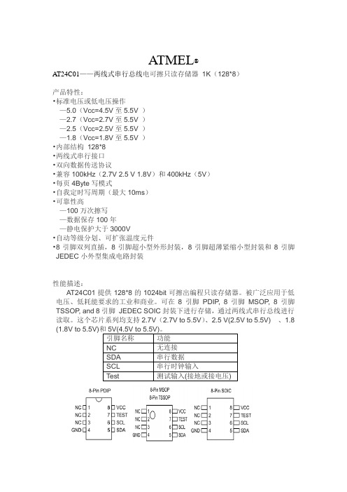
ATMEL®AT24C01——两线式串行总线电可擦只读存储器1K(128*8)产品特性:•标准电压或低电压操作—5.0(Vcc=4.5V至5.5V )—2.7(Vcc=2.7V至5.5V )—2.5(Vcc=2.5V至5.5V )—1.8(Vcc=1.8V至5.5V )•内部结构128*8•两线式串行接口•双向数据传送协议•兼容100kHz(2.7V 2.5 V 1.8V)和400kHz(5V)•每页4Byte写模式•自我定时写周期(最大10ms)•可靠性高—100万次擦写—数据保存100年—静电保护大于3000V•自动等级分划、可扩张温度元件•8引脚双列直插,8引脚超小型外形封装,8引脚超薄紧缩小型封装和8引脚JEDEC小外型集成电路封装性能描述:AT24C01提供128*8的1024bit可擦出编程只读存储器。
被广泛应用于低电压、低耗能要求的工业和商业。
可在8引脚PDIP, 8引脚MSOP, 8引脚TSSOP, and 8引脚JEDEC SOIC封装下进行存储,通过两线式串行总线进行读取。
这个芯片系列均支持2.7V(2.7V to 5.5V)、2.5 V(2.5V to 5.5V) 、1.8 (1.8V to 5.5V)和5V(4.5V to 5.5V)。
引脚名称功能NC 无连接SDA 串行数据SCL 串行时钟输入Test 测试输入(接地或接电压)绝对最大功率:运行温度…………-55°至+125°存储温度…………-65°至+150°引脚承受最高电压…………-1V至+7V运行最大电压…………6.25V直流最大电流…………5.0mA*注意:超过上述参数工作会损坏本元件,这是唯一的功能操作参数,超过此功率将不被支持。
按照额定功率工作将使元件更加可靠。
模块图引脚描述:SERIAL CLOCK (SCL):SCL引脚在电压上升沿时输入数据,下降沿时输出数据SERIAL DATA (SDA):SDA引脚用作双向传送数据,高电平驱动可能与其它任何引脚或元件进行线或运算。
AT24C11-10TI-1.8;AT24C11-10TI-2.7;AT24C11-10TU-1.8;中文规格书,Datasheet资料

Features•Low Voltage and Standard Voltage Operation–2.7 (V CC = 2.7V to 5.5V)–1.8 (V CC = 1.8V to 5.5V)•Internally Organized 128 x 8•Two-wire Serial Interface•Bidirectional Data Transfer Protocol•400 kHz (1.8V) and 1 MHz (2.5V, 2.7V, 5V) Compatibility •4-Byte Page Write Mode•Self-Timed Write Cycle (5 ms max)•High Reliability–Endurance: 1 Million Write Cycles –Data Retention: 100 Years•Automotive Grade, Extended Temperature and Lead-Free/Halogen-Free Devices Available•8-lead PDIP , 8-lead JEDEC SOIC, 5-lead SOT23 and 8-lead TSSOP Packages •Die Sales: Wafer Form, Waffle Pack, and Bumped Wafers •Access to One Additional Page Upon RequestDescriptionThe AT24C11 provides 1024 bits of serial electrically erasable and programmable read only memory (EEPROM) organized as 128 words of 8 bits each. The device is optimized for use in many industrial and commercial applications where low power and low voltage operation are essential. The AT24C11 is available in space saving 8-lead PDIP, 8-lead JEDEC SOIC, 5-lead SOT23 and 8-lead TSSOP packages and is accessed via a two-wire serial interface. In addition, the entire family is available in 2.7V (2.7V to 5.5V) and 1.8V (1.8V to 5.5V) versions.Table 0-1.Pin ConfigurationPin Name Function NC No Connect SDA Serial Data SCL Serial Clock Input TESTTest Input (GND or VCC)Two-wire Serial EEPROM1K (128 x 8)AT24C11Note:Not recommended for new design; please refer to AT24C01B datasheet.Rev. 3409G–SEEPR–8/078-lead PDIP8-lead SOIC8-lead TSSOP23409G–SEEPR–8/07AT24C11Figure 0-1.Block Diagram 1.Pin DescriptionSERIAL CLOCK (SCL): The SCL input is used to positive edge clock data into each EEPROM device and negative edge clock data out of each device.SERIAL DATA (SDA): The SDA pin is bidirectional for serial data transfer. This pin is open-drain driven and may be wire-ORed with any number of other open-drain or open collector devices.Absolute Maximum Ratings*Operating Temperature..................................–55°C to +125°C *NOTICE:Stresses beyond those listed under “Absolute Maximum Ratings” may cause permanent dam-age to the device. This is a stress rating only and functional operation of the device at these or any other conditions beyond those indicated in the operational sections of this specification is not implied. Exposure to absolute maximum rating conditions for extended periods may affect device reliability.Storage Temperature.....................................–65°C to +150°C Voltage on Any Pinwith Respect to Ground....................................–1.0V to +7.0V Maximum Operating Voltage..........................................6.25V DC Output Current........................................................5.0 mA33409G–SEEPR–8/07AT24C112.Memory OrganizationAT24C11, 1K SERIAL EEPROM: Internally organized with 32 pages of 4 bytes each. The 1K requires a 7-bit data word address for random word addressing. Access to one additional page (33rd page) available upon request.Note:1.V IL min and V IH max are reference only and are not tested.Table 2-1.Pin CapacitanceApplicable over recommended operating range from T A = 25°C, f = 1.0 MHz, V CC = +1.8V.Symbol Test ConditionMax Units Condition C I/O Input/Output Capacitance (SDA)8pF V I/O = 0V C INInput Capacitance (A0, A1, A2, SCL)6pFV IN = 0VTable 2-2.DC CharacteristicsApplicable over recommended operating range from: T AI = –40°C to +85°C, V CC = +1.8V to +5.5V, V CC =+2.7V to +5.5V (unless otherwise noted)Symbol Parameter Test ConditionMin TypMax Units V CC1Supply Voltage 1.8 5.5V V CC2Supply Voltage 2.5 5.5V V CC3Supply Voltage 2.7 5.5V V CC4Supply Voltage4.55.5V I CC Supply Current V CC = 5.0V READ at 100 kHz 0.4 1.0mA I CC Supply Current V CC = 5.0V WRITE at 100 kHz 2.0 3.0mA I SB1Standby Current V CC = 1.8V V IN = V CC or V SS 0.6 3.0µA I SB2Standby Current V CC = 2.5V V IN = V CC or V SS 1.4 4.0µA I SB3Standby Current V CC = 2.7V V IN = V CC or V SS 1.6 4.0µA I SB4Standby Current V CC = 5.0V V IN = V CC or V SS 8.018.0µA I LI Input Leakage Current V IN = V CC or V SS 0.10 3.0µA I LO Output Leakage Current V OUT = V CC or V SS0.05 3.0µA V IL Input Low Level (1)–0.6V CC × 0.3V V IH Input High Level (1)V CC × 0.7V CC + 0.5V V OL2Output Low Level V CC = 3.0V I OL = 2.1 mA 0.4V V OL1Output Low Level V CC = 1.8VI OL = 0.15 mA 0.2V43409G–SEEPR–8/07AT24C11Note:1.This parameter is characterized and is not 100% tested.Table 2-3.AC CharacteristicsApplicable over recommended operating range from T AI = –40°C to +85°C, V CC = +1.8V to +5.5V, V CC = +2.7V to +5.5V, CL = 1 TTL Gate and 100pF (unless otherwise noted)Symbol Parameter1.8V2.7V, 2.5V, 5.0V Units MinMax MinMax f SCL Clock Frequency, SCL 4001000kHz t LOW Clock Pulse Width Low 1.20.4µs t HIGH Clock Pulse Width High 0.60.4µs t AA Clock Low to Data Out Valid0.10.90.050.55µs t BUF Time the bus must be free before a new transmission can start (1) 1.20.5µs t HD.STA Start Hold Time 0.60.25µs t SU.STA Start Set-up Time 0.60.6µs t HD.DAT Data In Hold Time 00µs t SU.DAT Data In Set-up Time 100100ns t R Inputs Rise Time (1)0.30.3µs t F Inputs Fall Time (1)300100ns t SU.STO Stop Set-up Time 0.60.25µs t DH Data Out Hold Time 5050ns t WRWrite Cycle Time 55ms Endurance (1) 5.0V, 25°C, Page Mode1M 1MWrite Cycles53409G–SEEPR–8/07AT24C113.Device OperationCLOCK and DATA TRANSITIONS: The SDA pin is normally pulled high with an external device. Data on the SDA pin may change only during SCL low time periods (see Figure 3-3 on page 7). Data changes during SCL high periods will indicate a start or stop condition as defined below.START CONDITION: A high-to-low transition of SDA with SCL high is a start condition which must precede any other command (see Figure 3-4 on page 7).STOP CONDITION: A low-to-high transition of SDA with SCL high is a stop condition which ter-minates all communications. After a read sequence, the stop command will place the EEPROM in a standby power mode (see Figure 3-4 on page 7).ACKNOWLEDGE: All addresses and data words are serially transmitted to and from the EEPROM in 8-bit words. Any device on the system bus receiving data (when communicating with the EEPROM) must pull the SDA bus low to acknowledge that it has successfully received each word. This must happen during the ninth clock cycle after each word received and after all other system devices have freed the SDA bus. The EEPROM will likewise acknowledge by pull-ing SDA low after receiving each address or data word (see Figure 3-5 on page 7).STANDBY MODE: The AT24C11 features a low power standby mode which is enabled: (a)upon power-up and (b) after the receipt of the STOP bit and the completion of any internal operations.MEMORY RESET: After an interruption in protocol, power loss or system reset, any 2-wire part can be reset by following these steps:(a) clock up to 9 cycles, (b) look for SDA high in each cycle while SCL is high and then (c) create a start condition as SDA is high.63409G–SEEPR–8/07AT24C11Figure 3-1.Bus TimingFigure 3-2.Write Cycle TimingSCL: Serial Clock, SDA: Serial Data I/ONote:1.The write cycle time t WRis the time from a valid stop condition of a write sequence to the end of the internal clear/write cycle.73409G–SEEPR–8/07AT24C11Figure 3-3.Data ValidityFigure 3-4.Start and Stop DefinitionFigure 3-5.Output Acknowledge83409G–SEEPR–8/07AT24C114.Write OperationsBYTE WRITE: Following a start condition, a write operation requires a 7-bit data word address and a low write bit. Upon receipt of this address, the EEPROM will again respond with a zero and then clock in the first 8-bit data word. Following receipt of the 8-bit data word, the EEPROM will output a zero and the addressing device, such as a microcontroller, must terminate the write sequence with a stop condition. At this time the EEPROM enters an internally-timed write cycle to the nonvolatile memory. All inputs are disabled during this write cycle, t WR , and the EEPROM will not respond until the write is complete (see Figure 5-1 on page 9).PAGE WRITE: The AT24C11 is capable of a 4-byte page write.A page write is initiated the same as a byte write but the microcontroller does not send a stop condition after the first data word is clocked in. Instead, after the EEPROM acknowledges receipt of the first data word, the microcontroller can transmit up to three more data words. The EEPROM will respond with a zero after each data word received. The microcontroller must ter-minate the page write sequence with a stop condition (see Figure 5-2 on page 9).The data word address lower 2 bits are internally incremented following the receipt of each data word. The higher five data word address bits are not incremented, retaining the memory page row location. When the word address, internally generated, reaches the page boundary, the fol-lowing byte is placed at the beginning of the same page. If more than four data words are transmitted to the EEPROM, the data word address will “roll over” and previous data will be overwritten. Access to 1 additional page is available upon request.ACKNOWLEDGE POLLING: Once the internally-timed write cycle has started and the EEPROM inputs are disabled, acknowledge polling can be initiated. This involves sending a start condition followed by the device address word. The read/write bit is representative of the operation desired. Only if the internal write cycle has completed will the EEPROM respond with a zero allowing the read or write sequence to continue.5.Read OperationsRead operations are initiated the same way as write operations with the exception that the read/write select bit in the device address word is set to one. There are two read operations:byte read and sequential read.BYTE READ: A byte read is initiated with a start condition followed by a 7-bit data word address and a high read bit. The AT24C11 will respond with an acknowledge and then serially output 8data bits. The microcontroller does not respond with a zero but does generate a following stop condition (see Figure 5-3 on page 9).SEQUENTIAL READ: Sequential reads are initiated the same as a byte read. After the micro-controller receives an 8-bit data word, it responds with an acknowledge. As long as the EEPROM receives an acknowledge, it will continue to increment the data word address and serially clock out sequential data words. When the memory address limit is reached, the data word address will “roll over” and the sequential read will continue. The sequential read operation is terminated when the microcontroller does not respond with an input zero but does generate a following stop condition (see Figure 5-4 on page 9).93409G–SEEPR–8/07AT24C11Figure 5-1.Byte WriteFigure 5-2.Page WriteFigure 5-3.Byte ReadFigure 5-4.Sequential Read103409G–SEEPR–8/07AT24C11Notes:1.For2.7V devices used in the 4.5V to 5.5V range, please refer to performance values in the AC and DC Characteristicstables.2.“U” designates Green package + RoHS compliant.3.Die sales available in waffle pack and wafer form, order as SL719 for wafer form. Bumped die sales available upon request.Please contact Serial EEPROM Marketing.AT24C11 Ordering Information (1)Ordering Code Package Operation Range AT24C11-10PI-2.7AT24C11N-10SI-2.7AT24C11-10TI-2.78P38S18A2Industrial Temperature (–40°C to 85°C)AT24C11-10PI-1.8AT24C11N-10SI-1.8AT24C11-10TI-1.88P38S18A2Industrial Temperature (–40°C to 85°C)AT24C11-10PU-2.7(2)AT24C11-10PU-1.8(2)AT24C11N-10SU-2.7(2)AT24C11N-10SU-1.8(2)AT24C11-10TU-2.7(2)AT24C11-10TU-1.8(2)AT24C11-10TSU-1.8(2)8P38P38S18S18A28A25TS1Lead-free/Halogen-free/Industrial Temperature (–40°C to 85°C)AT24C11-W2.7-11(3)AT24C11-W1.8-11(3)Die Sale Die SaleIndustrial Temperature (–40°C to 85°C)Package Type8P38-lead, 0.300" Wide, Plastic Dual Inline Package (PDIP)8S18-lead, 0.150" Wide, Plastic Gull Wing Small Outline (JEDEC SOIC)8A28-lead, 4.4 mm Body, Plastic, Thin Shrink Small Outline Package (TSSOP)5TS15-lead, 2.90 mm x 1.60 mm Body, Plastic Thin Shrink Small Outline Package (SOT23)Options–2.7Low-Voltage (2.7V to 5.5V)–1.8Low-Voltage (1.8V to 5.5V)分销商库存信息:ATMELAT24C11-10PI-1.8AT24C11-10PI-2.7AT24C11-10TI-1.8 AT24C11-10TI-2.7AT24C11-10TU-1.8AT24C11-10TU-2.7 AT24C11N-10SI-1.8AT24C11N-10SI-2.7AT24C11N-10SU-1.8 AT24C11N-10SU-2.7AT24C11-10PU-1.8AT24C11-10PU-2.7 AT24C11N-10SI-2.7 SL383AT24C11N-10SU-2.7AT24C11-10TSU-1.8SL383AT24C11Y1-10YU-1.8。
AT24C08A-10PE-2.7中文资料
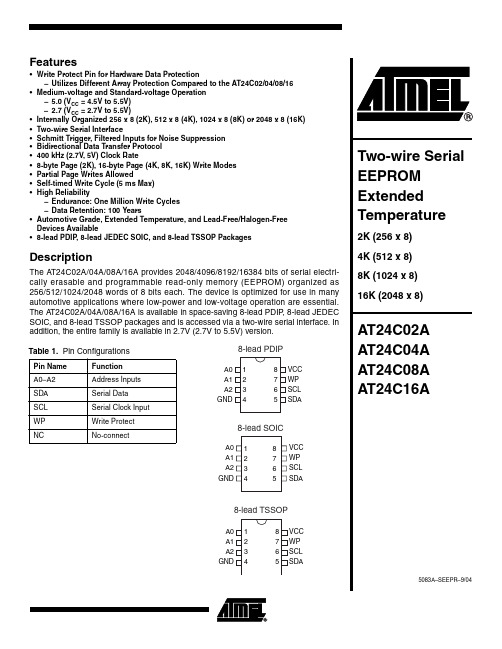
1Features•Write Protect Pin for Hardware Data Protection –Utilizes Different Array Protection Compared to the AT24C02/04/08/16•Medium-voltage and Standard-voltage Operation –5.0 (V CC = 4.5V to 5.5V)–2.7 (V CC = 2.7V to 5.5V)•Internally Organized 256 x 8 (2K), 512 x 8 (4K), 1024 x 8 (8K) or 2048 x 8 (16K)•Two-wire Serial Interface•Schmitt Trigger, Filtered Inputs for Noise Suppression •Bidirectional Data Transfer Protocol •400 kHz (2.7V, 5V) Clock Rate•8-byte Page (2K), 16-byte Page (4K, 8K, 16K) Write Modes •Partial Page Writes Allowed•Self-timed Write Cycle (5 ms Max)•High Reliability–Endurance: One Million Write Cycles –Data Retention: 100 Years•Automotive Grade, Extended Temperature, and Lead-Free/Halogen-Free Devices Available•8-lead PDIP , 8-lead JEDEC SOIC, and 8-lead TSSOP PackagesDescriptionThe AT24C02A/04A/08A/16A provides 2048/4096/8192/16384 bits of serial electri-cally erasable and programmable read-only memory (EEPROM) organized as 256/512/1024/2048 words of 8 bits each. The device is optimized for use in many automotive applications where low-power and low-voltage operation are essential.The A T24C02A/04A/08A/16A is available in space-saving 8-lead PDIP , 8-lead JEDEC SOIC, and 8-lead TSSOP packages and is accessed via a two-wire serial interface. In addition, the entire family is available in 2.7V (2.7V to 5.5V) version.Table 1. Pin Configurations2AT24C02A/04A/08A/16A5083A–SEEPR–9/04Figure 1. Block DiagramPin DescriptionSERIAL CLOCK (SCL): The SCL input is used to positive edge clock data into each EEPROM device and negative edge clock data out of each device.SERIAL DATA (SDA): The SDA pin is bidirectional for serial data transfer. This pin is open-drain driven and may be wire-ORed with any number of other open-drain or open-collector devices.DEVICE/PAGE ADDRESSES (A2, A1, A0): The A2, A1, and A0 pins are device address inputs that must be hardwired for the AT24C02A. As many as eight 2K devices may be addressed on a single bus system. (Device addressing is discussed in detail under Device Addressing, page 9).The AT24C04A uses the A2 and A1 inputs for hardwire addressing, and a total of four 4K devices may be addressed on a single bus system. The A0 pin is a no-connect.Absolute Maximum Ratings**NOTICE:Stresses beyond those listed under “Absolute Maximum Ratings” may cause permanent dam-age to the device. This is a stress rating only and functional operation of the device at these or any other conditions beyond those indicated in the operational sections of this specification is not implied. Exposure to absolute maximum rating conditions for extended periods may affect device reliability.3AT24C02A/04A/08A/16A5083A–SEEPR–9/04The AT24C08A only uses the A2 input for hardwire addressing, and a total of two 8K devices may be addressed on a single bus system. The A0 and A1 pins are no-connects.The AT24C16A does not use the device address pins, which limits the number of devices on a single bus to one. The A0, A1, and A2 pins are no-connects.WRITE PROTECT (WP): The AT24C02A/04A/08A/16A have a WP pin that provides hardware data protection. The WP pin allows normal read/write operations when con-nected to ground (GND). When the WP pin is connected to V CC , the write protection feature is enabled and operates as shown. (See Table 1.)Table 1. Write ProtectMemory OrganizationAT24C02A, 2K SERIAL EEPROM: The 2K is internally organized with 32 pages of 8bytes each. Random word addressing requires an 8-bit data word address.AT24C04A, 4K SERIAL EEPROM: The 4K is internally organized with 32 pages of 16bytes each. Random word addressing requires a 9-bit data word address.AT24C08A, 8K SERIAL EEPROM: The 8K is internally organized with 64 pages of 16bytes each. Random word addressing requires a 10-bit data word address.AT24C16A, 16K SERIAL EEPROM: The 16K is internally organized with 128 pages of 16 bytes each. Random word addressing requires an 11-bit data word address.Note:This parameter is characterized and is not 100% tested.Table 2. Pin Capacitance4AT24C02A/04A/08A/16A5083A–SEEPR–9/04Note:1.V IL min and V IH max are reference only and are not tested.Table 3. DC CharacteristicsApplicable over recommended operating range from: T AE = −40°C to +125°C, V CC = +2.7V to +5.5V5AT24C02A/04A/08A/16A5083A–SEEPR–9/04Note:1.This parameter is characterized and is not 100% tested (T A = 25°C).2.This parameter is characterized and is not 100% tested.Table 4. AC CharacteristicsApplicable over recommended operating range from T AE = −40°C to +125°C, V CC = +2.7V to +5.5V, CL = 1 TTL Gate and 100 pF (unless otherwise noted).6AT24C02A/04A/08A/16A5083A–SEEPR–9/04Device OperationCLOCK and DATA TRANSITIONS: The SDA pin is normally pulled high with an exter-nal device. Data on the SDA pin may change only during SCL low time periods (see Figure 2). Data changes during SCL high periods will indicate a start or stop condition as defined in Figure 2.Figure 2. Data ValiditySTART CONDITION: A high-to-low transition of SDA with SCL high is a start condition that must precede any other command (see Figure 3).Figure 3. Start and Stop DefinitionSTOP CONDITION: A low-to-high transition of SDA with SCL high is a stop condition.After a read sequence, the stop command will place the EEPROM in a standby power mode (see Figure 3).ACKNOWLEDGE: All addresses and data words are serially transmitted to and from the EEPROM in 8-bit words. The EEPROM sends a “0” to acknowledge that it has received each word. This happens during the ninth clock cycle.STANDBY MODE: The AT24C02A/04A/08A/16A features a low-power standby mode that is enabled (a) upon power-up and (b) after the receipt of the STOP bit and the com-pletion of any internal operations.7AT24C02A/04A/08A/16A5083A–SEEPR–9/04MEMORY RESET: After an interruption in protocol, power loss or system reset, any two-wire part can be reset by following these steps:1.Clock up to 9 cycles.2.Look for SDA high in each cycle while SCL is high.3.Create a start condition as SDA is high.Figure 4. Bus TimingFigure 5. Write Cycle TimingNote:The write cycle time t WRis the time from a valid stop condition of a write sequence to the end of the interval clear/write cycle.8AT24C02A/04A/08A/16A5083A–SEEPR–9/04Figure 6.Output Acknowledge9AT24C02A/04A/08A/16A5083A–SEEPR–9/04Device AddressingThe 2K, 4K, and 8K EEPROM devices all require an 8-bit device address word following a start condition to enable the chip for a read or write operation, as shown in Figure 7.Figure 7. Device AddressThe device address word consists of a mandatory “1”, “0” sequence for the first four most significant bits as shown. This is common to all the EEPROM devices.The next three bits are the A2, A1, and A0 device address bits for the 2K EEPROM.These three bits must compare to their corresponding hardwired input pins.The 4K EEPROM only uses the A2 and A1 device address bits with the third bit being a memory page address bit. The two device address bits must compare to their corre-sponding hardwired input pins. The A0 pin is no-connect.The 8K EEPROM only uses the A2 device address bit with the next two bits being for memory page addressing. The A2 bit must compare to its corresponding hardwired input pin. The A1 and A0 pins are no-connect.The 16K EEPROM does not use the device address pins, which limits the number of devices on a single bus to one. The A0, A1, and A2 pins are no-connects.The eighth bit of the device address is the read/write operation select bit. A read opera-tion is initiated if this bit is high, and a write operation is initiated if this bit is low.Upon a compare of the device address, the EEPROM will output a “0”. If a compare is not made, the chip will return to a standby state.Write OperationsBYTE WRITE: A write operation requires an 8-bit data word address following the device address word and acknowledgement. Upon receipt of this address, the EEPROM will again respond with a “0” and then clock in the first 8-bit data word. Following receipt of the 8-bit data word, the EEPROM will output a “0” and the addressing device, such as a microcontroller, must terminate the write sequence with a stop condition. At this time,the EEPROM enters an internally-timed write cycle, t WR , to the nonvolatile memory. All inputs are disabled during this write cycle, and the EEPROM will not respond until the write is complete, as shown in Figure 8.10AT24C02A/04A/08A/16A5083A–SEEPR–9/04Figure 8. Byte WritePAGE WRITE: The 2K EEPROM is capable of an 8-byte page write, and the 4K, 8K,and 16K devices are capable of 16-byte page writes.A page write is initiated the same as a byte write, but the microcontroller does not send a stop condition after the first data word is clocked in. Instead, after the EEPROM acknowledges receipt of the first data word, the microcontroller can transmit up to seven (2K) or fifteen (4K, 8K, 16K) more data words. The EEPROM will respond with a “0”after each data word received. The microcontroller must terminate the page write sequence with a stop condition, as shown in Figure 9.Figure 9. Page WriteThe data word address lower three (2K) or four (4K, 8K, 16K) bits are internally incre-mented following the receipt of each data word. The higher data word address bits are not incremented, retaining the memory page row location. When the word address,internally generated, reaches the page boundary, the following byte is placed at the beginning of the same page. If more than eight (2K) or sixteen (4K, 8K, 16K) data words are transmitted to the EEPROM, the data word address will “roll over” and previous data will be overwritten.ACKNOWLEDGE POLLING: Once the internally-timed write cycle has started and the EEPROM inputs are disabled, acknowledge polling can be initiated. This involves send-ing a start condition followed by the device address word. The read/write bit is representative of the operation desired. Only if the internal write cycle has completed will the EEPROM respond with a “0” allowing the read or write sequence to continue.11AT24C02A/04A/08A/16A5083A–SEEPR–9/04Read OperationsRead operations are initiated the same way as write operations with the exception that the read/write select bit in the device address word is set to “1”. There are three read operations: current address read, random address read and sequential read.CURRENT ADDRESS READ: The internal data word address counter maintains the last address accessed during the last read or write operation, incremented by one. This address stays valid between operations as long as the chip power is maintained. The address “roll over” during read is from the last byte of the last memory page to the first byte of the first page. The address “roll over” during write is from the last byte of the cur-rent page to the first byte of the same page.Once the device address with the read/write select bit set to “1” is clocked in and acknowledged by the EEPROM, the current address data word is serially clocked out.The microcontroller does not respond with an input “0” but does generate a following stop condition, as shown in Figure 10.Figure 10. Current Address ReadRANDOM READ: A random read requires a “dummy” byte write sequence to load in the data word address. Once the device address word and data word address are clocked in and acknowledged by the EEPROM, the microcontroller must generate another start condition. The microcontroller now initiates a current address read by sending a device address with the read/write select bit high. The EEPROM acknowledges the device address and serially clocks out the data word. The microcontroller does not respond with a “0” but does generate a following stop condition, as shown in Figure 11.Figure 11. Random ReadSEQUENTIAL READ: Sequential reads are initiated by either a current address read or a random address read. After the microcontroller receives a data word, it responds with an acknowledge. As long as the EEPROM receives an acknowledge, it will continue to increment the data word address and serially clock out sequential data words. When the memory address limit is reached, the data word address will “roll over” and the sequen-tial read will continue. The sequential read operation is terminated when the12AT24C02A/04A/08A/16A5083A–SEEPR–9/04microcontroller does not respond with a “0” but does generate a following stop condition,as shown in Figure 12.Figure 12.Sequential Read13AT24C02A/04A/08A/16A5083A–SEEPR–9/04Note:For 2.7V devices used in the 4.5V to 5.5V range, please refer to performance values in the AC and DC characteristics tables (Table 3 on page 4 and Table 4 on page 5).AT24C02A Ordering Information14AT24C02A/04A/08A/16A5083A–SEEPR–9/04Note:For 2.7V devices used in the 4.5V to 5.5V range, please refer to performance values in the AC and DC characteristics tables (Table 3 on page 4 and Table 4 on page 5).AT24C04A Ordering Information15AT24C02A/04A/08A/16A5083A–SEEPR–9/04Note:For 2.7V devices used in the 4.5V to 5.5V range, please refer to performance values in the AC and DC characteristics tables (Table 3 on page 4 and Table 4 on page 5).AT24C08A Ordering Information16AT24C02A/04A/08A/16A5083A–SEEPR–9/04Note:For 2.7V devices used in the 4.5V to 5.5V range, please refer to performance values in the AC and DC characteristics table (Table 3 on page 4 and Table 4 on page 5).AT24C16A Ordering Information17AT24C02A/04A/08A/16A5083A–SEEPR–9/04Packaging Information8P3 – PDIP18AT24C02A/04A/08A/16A5083A–SEEPR–9/048S1 – JEDEC SOIC19AT24C02A/04A/08A/16A5083A–SEEPR–9/048A2 – TSSOP5083A–SEEPR–9/04Disclaimer: The information in this document is provided in connection with Atmel products. No license, express or implied, by estoppel or otherwise,to any intellectual property right is granted by this document or in connection with the sale of Atmel products. EXCEPT AS SET FORTH IN ATMEL ’S TERMS AND CONDI-TIONS OF SALE LOCATED ON ATMEL ’S WEB SITE, ATMEL ASSUMES NO LIABILITY WHATSOEVER AND DISCLAIMS ANY EXPRESS, IMPLIED OR STATUTORY WARRANTY RELATING TO ITS PRODUCTS INCLUDING, BUT NOT LIMITED TO, THE IMPLIED WARRANTY OF MERCHANTABILITY, FITNESS FOR A PARTICULAR PURPOSE, OR NON-INFRINGEMENT. IN NO EVENT SHALL ATMEL BE LIABLE FOR ANY DIRECT, INDIRECT, CONSEQUENTIAL, PUNITIVE, SPECIAL OR INCIDEN-TAL DAMAGES (INCLUDING, WITHOUT LIMITATION, DAMAGES FOR LOSS OF PROFITS, BUSINESS INTERRUPTION, OR LOSS OF INFORMATION) ARISING OUT OF THE USE OR INABILITY TO USE THIS DOCUMENT, EVEN IF ATMEL HAS BEEN ADVISED OF THE POSSIBILITY OF SUCH DAMAGES. Atmel makes no representations or warranties with respect to the accuracy or completeness of the contents of this document and reserves the right to make changes to specifications and product descriptions at any time without notice. Atmel does not make any commitment to update the information contained herein. Atmel’s products are not intended, authorized, or warranted for use as components in applications intended to support or sustain life.Atmel CorporationAtmel Operations2325 Orchard Parkway San Jose, CA 95131, USA Tel: 1(408) 441-0311Fax: 1(408) 487-2600Regional HeadquartersEuropeAtmel SarlRoute des Arsenaux 41Case Postale 80CH-1705 Fribourg SwitzerlandTel: (41) 26-426-5555Fax: (41) 26-426-5500AsiaRoom 1219Chinachem Golden Plaza 77 Mody Road Tsimshatsui East Kowloon Hong KongTel: (852) 2721-9778Fax: (852) 2722-1369Japan9F, Tonetsu Shinkawa Bldg.1-24-8 ShinkawaChuo-ku, Tokyo 104-0033JapanTel: (81) 3-3523-3551Fax: (81) 3-3523-7581Memory2325 Orchard Parkway San Jose, CA 95131, USA Tel: 1(408) 441-0311Fax: 1(408) 436-4314Microcontrollers2325 Orchard Parkway San Jose, CA 95131, USA Tel: 1(408) 441-0311Fax: 1(408) 436-4314La Chantrerie BP 7060244306 Nantes Cedex 3, France Tel: (33) 2-40-18-18-18Fax: (33) 2-40-18-19-60ASIC/ASSP/Smart CardsZone Industrielle13106 Rousset Cedex, France Tel: (33) 4-42-53-60-00Fax: (33) 4-42-53-60-011150 East Cheyenne Mtn. Blvd.Colorado Springs, CO 80906, USA Tel: 1(719) 576-3300Fax: 1(719) 540-1759Scottish Enterprise Technology Park Maxwell BuildingEast Kilbride G75 0QR, Scotland Tel: (44) 1355-803-000Fax: (44) 1355-242-743RF/AutomotiveTheresienstrasse 2Postfach 353574025 Heilbronn, Germany Tel: (49) 71-31-67-0Fax: (49) 71-31-67-23401150 East Cheyenne Mtn. Blvd.Colorado Springs, CO 80906, USA Tel: 1(719) 576-3300Fax: 1(719) 540-1759Biometrics/Imaging/Hi-Rel MPU/High Speed Converters/RF DatacomAvenue de Rochepleine BP 12338521 Saint-Egreve Cedex, France Tel: (33) 4-76-58-30-00Fax: (33) 4-76-58-34-80Literature Requests/literature© Atmel Corporation 2004. All rights reserved. Atmel ®, logo and combinations thereof are registered trademarks and Everywhere Y ou Are SM is a trademark of Atmel Corporation or its subsidiaries. Other terms and product names may be the trademarks of others.。
- 1、下载文档前请自行甄别文档内容的完整性,平台不提供额外的编辑、内容补充、找答案等附加服务。
- 2、"仅部分预览"的文档,不可在线预览部分如存在完整性等问题,可反馈申请退款(可完整预览的文档不适用该条件!)。
- 3、如文档侵犯您的权益,请联系客服反馈,我们会尽快为您处理(人工客服工作时间:9:00-18:30)。
最小 1,000,000 100 2000 100
最大
单位 周期/字节 年 V mA
参考测试模式 MIL-STD-883 测试方法 1033 MIL-STD-883 测试方法 1008 MIL-STD-883 测试方法 3015 JEDEC 标准 17
3
广州周立功单片机发展有限公司 Tel
020
38730976
38730977
Fax 38730925
直流操作特性 Vcc=+1.8V 符号 ICC ISB ILI ILO VIL VIH VOL1 VOL2 +6.0V 除非特别说明 最小 典型 最大 3 0 10 10 1 Vcc 0.7 Vcc 0.3 Vcc+0.5 0.4 0.5 单位 mA A A A V V V V IOL=3 mA IOL=1.5 mA 测试条件 FSCL=100KHz VIN=0 ~Vcc VIN=0 ~Vcc VOUT=0 ~Vcc 参数 电源电流 备用电流(Vcc=5.0V) 输入漏电流 输出漏电流 输入低电压 输入高电压 输出低电压 输出低电压
1
广州周立功单片机发展有限公司 Tel
020
38730976
38730977
Fax 38730925
CAT24WC01/02/04/08/16 1K/2K/4K/8K/16K 位串行 E PROM
2
特性
I2C 总线协议
I2C 总线协议定义如下
5
广州周立功单片机发展有限公司 Tel
020
38730976
38730977
Fax 38730925
1 只有在总线空闲时才允许启动数据传送 2 在数据传送过程中 钟线为高电平时 起始信号 时钟线保持高电平期间 数据线电平从高到低的跳变作为 I2C 总线的起始信号 停止信号 时钟线保持高电平期间 数据线电平从低到高的跳变作为 I2C 总线的停止信号 图1 总线时序 当时钟线为高电平时 数据线必须保持稳定状态 不允许有跳变 时 数据线的任何电平变化将被看作总线的起始或停止信号
管脚描述
SCL 入管脚 SDA 输出管脚 A0 A1 串行数据/地址 可与其它开漏输出或集电极开路输出进行线或 A2 器件地址输入端 当这些脚悬空时默认值为 0 24WC01 除外 wire-OR CAT24WC01/02/04/08/16 双向串行数据/地址管脚用于器件所有数据的发送或接收 SDA 是一个开漏 串行时钟 CAT24WC01/02/04/08/16 串行时钟输入管脚用于产生器件所有数据发送或接收的时钟 这是一个输
方框图
极限参数
工作温度 工业级 -55 +125 商业级 0 +75 贮存温度 -65 +150 各管脚承受电压 -2.0 Vcc+2.0V Vcc 管脚承受电压 -2.0 +7.0V 封装功率损耗 Ta=25 1.0W 焊接温度(10 秒) 300 输出短路电流 100mA 可靠性参数 符号 参数 NEND 耐久性 TDR 数据保存时间 VZAP ESD ILTH 上拉电流
CAT24WC01/02/04/08/16 监视总线并当其地址与发送的从地址相符时响应一个应答信号 通过 SDA 线 CAT24WC01/02/04/08/16 再根据读写控制位 R/W 的状态进行读或写操作 应答信号 I2C 总线数据传送时 每成功地传送一个字节数据后 接收器都必须产生一个应答信号 应答的器 件在第 9 个时钟周期时将 SDA 线拉低 表示其已收到一个 8 位数据 CAT24WC01/02/04/08/16 在接收到起始信号和从器件地址之后响应一个应答信号 如果器件已选择 了写操作 则在每接收一个 8 位字节之后响应一个应答信号 当 CAT24WC01/02/04/08/16 工作于读模式时 在发送一个 8 位数据后释放 SDA 线并监视一个应答 信号 一旦接收到应答信号 CAT24WC01/02/04/08/16 继续发送数据 如主器件没有发送应答信号 器 件停止传送数据且等待一个停止信号 图 4 应答时序
分布电容 TA=25 , f =1.0MHz, Vcc =5V 测试项 I/O 电容 SDA 脚 输出电容 A0 A1 A2 SCL WP 最大 8 6 单位 PF PF 条件 VI/O=0V VIN=0V 符号 CI/O CIN 交流特性 Vcc=+1.8V +6.0V 除非特别说明 输出负载能力为 1 个 TTL 门和 100pF 读写周期范围 符号 FSCL TI tAA tBUF tHD: STA tLOW tHIGH tSU: STA tHD: DAT tSUl: DAT tR tF tSU: STO tDH 时钟频率 SCL,SDA 输入的噪声抑制时间 SCL 变低至 SDA 数据输出及应答信号 新的发送开始前总线空闲时间 起始信号保持时间 时钟低电平周期 时钟高电平周期 起始信号建立时间 数据输入保持时间 数据输入建立时间 SDA 及 SCL 上升时间 SDA 及 SCL 下降时间 停止信号建立时间 数据输出保持时间 4 100 4.7 4 4.7 4 4.7 0 50 1 300 0.6 100 参数 1.8 V 最小 2.5 V 最大 100 200 3.5 1.2 0.6 1.2 0.6 0.6 0 50 0.3 300 4.5V 最小 5.5V 最大 400 200 1 单位 KHz ns s s s s s s ns ns s ns s ns
图5
从器件地址位
1. 2.
A0 A1 和 A2 对应器件的管脚 1 2 和 3 a8 a9 和 a10 对应存储阵列地址字地址
7
广州周立功单片机发展有限公司 Tel
020
38730976
38730977
Fax 38730925
写操作
字节写 在字节写模式下 主器件发送起始命令和从器件地址信息 R/W 位置零 给从器件 在从器件产生 应答信号后 主器件发送 CAT24WC01/02/04/08/16 的字节地址 主器件在收到从器件的另一个应答信号 后 再发送数据到被寻址的存储单元 CAT24WC01/02/04/08/16 再次应答 并在主器件产生停止信号后 CAT24WC01/02/04/08/16 不再应答主器件的任何请求 图6 字节写时序 开始内部数据的擦写 在内部擦写过程中
4
广州周立功单片机发展有限公司 Tel
020
38730976
38730977
Fax 38730925
上电时序 符号 tPUR tPUW 写周期限制 符号 参数 最小 典型 最大 单位 写周期时间 tWR 10 ms 写周期时间是指从一个写时序的有效停止信号到内部编程/擦除周期结束的这一段时间 在写周期期 间 总线接口电路禁能 SDA 保持为高电平 器件不响应外部操作 参数 上电到读操作 上电到写操作 最大 1 1 单位 ms ms
概述
CAT24WC01/02/04/08/16 是 一 个 1K/2K/4K/8K/16K 位 串 行 CMOS E2PROM 128/256/512/1024/2048 个 8 位字节 内部含有 CATALYST 公司的先进 CMOS 技术实质上减少了器件的功耗
CAT24WC01 有一个 8 字节页写缓冲器 CAT24WC02/04/08/16 有一个 16 字节页写缓冲器 该器件通过 I2C 总线接口进行操作 有一个专门的写保护功能
这些输入脚用于多个器件级联时设置器件地址
当使用 24WC01 或 24WC02 时最大可级联 8 个器件 如果只有一个 24WC02 被总线寻址 这三个地 址输入脚 A0 A1 A2 可悬空或连接到 Vss 如果只有一个 24WC01 被总线寻址 这三个地址输入 脚 A0 A1 A2 必须连接到 Vss 如果只有一个 24WC04 被总线寻址 A1 和 A2 地址管脚可悬空或连接到 Vss 当使用 24WC04 时最多可连接 4 个器件 该器件仅使用 A1 A2 地址管脚 A0 管脚未用 可以连 接到 Vss 或悬空 Vss 或悬空 Vss 或悬空 WP 写保护 当 WP 管脚连接到 Vss 或悬空 允许 如果 WP 管脚连接到 Vcc 所有的内容都被写保护 只能读 器件进行正常的读/写操作 当使用 24WC08 时最多可连接 2 个器件 且仅使用地址管脚 A2 A0 A1 管脚未用 可以连接到 如果只有一个 24WC08 被总线寻址 A2 管脚可悬空或连接到 Vss 管脚可以连接到 当使用 24WC16 时最多只可连接 1 个器件 所有地址管脚 A0 A1 A2 都未用
功能描述
CAT24WC01/02/04/08/16 支持 I2C 总线数据传送协议 I2C 总线协议规定 任何将数据传送到总线的 器件作为发送器 任何从总线接收数据的器件为接收器 数据传送是由产生串行时钟和所有起始停止信 号的主器件控制的 主器件和从器件都可以作为发送器或接收器 但由主器件控制传送数据 发送或接 收 的模式 通过器件地址输入端 A0 A1 和 A2 可以实现将最多 8 个 24WC01 和 24WC02 器件 4 个 242C04 器件,2 个 24WC08 器件和 1 个 24WC16 器件连接到总线上
页写 用页写 CAT24WC01 可一次写入 8 个字节数据 CAT24WC02/04/08/16 可以一次写入 16 个字节的 数据 页写操作的启动和字节写一样 不同在于传送了一字节数据后并不产生停止信号 主器件被允许 发送 P CAT24WC01 P=7 CAT24WC02/04/08/16 P=15 个额外的字节 每发送一个字节数据后 先前写入的数据被 CAT24WC01/02/04/08/16 产生一个应答位并将字节地址低位加 1 高位保持不变 如果在发送停止信号之前主器件发送超过P+1个字节 覆盖 接收到P+1字节数据和主器件发送的停止信号后 CAT24CXXX启动内部写周期将数据写到数据区 所 有接收的数据在一个写周期内写入CAT24WC01/02/04/08/16 图 7 页写时序 地址计数器将自动翻转