逆变器控制
离网逆变器控制策略
逆变器控制策略:逆变器的控制目标是提高逆变器输出电压的稳态和动态性能。
稳态性能主要是指输出电 压的稳态精度和提高带不平衡负载的能力;动态性能主要是指输出电压的THD 和负载突变时的动态响应水平。
在这些指标中输出电压THD 要求比较高,对于三相逆变器,一般要求阻性负载满载时THD 小于2%,非线性满载(整流性负载)的THD 小于5%。
1、离网逆变器的控制性能要求主要是使其输出电压具有良好的控制抗扰性。
离网逆变器采用输出电容电流内环和输出电压外环的双闭环控制。
电流调节器可以实现快速加减速和电流限幅作用,同时使系统的抗电源扰动和负载扰动 的能力增强。
电压调节器主要是控制输出电压的稳定。
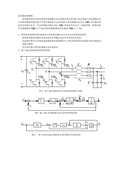
2、基于LC 滤波器的离网型逆变器图2 基于LC 滤波的电压型离网逆变器主电路图3 基于LC 的VSI 输出电压单闭环控制结构图5 基于电容电流反馈的单位调节器内环控制结构1VD 3VD 5VD 2VD 6VD 4VD 1V 3V 5V 4V 6V 2V U V WdcCCRLdc u +-L i o i C i L u Cu i u 调节器PWMK 1sL R +-i u o i C *u C u L i -1sC -C i ⊗⊗⊗Cu L u *Cq u cq u PI P PWMK 1sL sC 1iq u C *i Ci ⊗⊗⊗⊗oqi +----图14 基于同步坐标系的LC-VSI 双环控制结构PI PIP PInv.Park Trans Inv.Clarke TransSPWM GeneratorClarkeTransPark TransClarkeTransPark Trans*qs U*sdU sdU qs U *sdI *qs Iq s I ds I as I βs I AU βs U as U BU AI BI11ov T s +11e T s +11oi T s +PI1Ls1CsP11oi T s +11ov T s +*Cqu C*iiqu oqi cqu Ci +-+-+-+-电流内环。
逆变器控制策略概述
从控制理论的角度来说,闭环系统性能与闭环极点密切相关。在状态空间的分析中,除了利用输出反馈以外,主要利用状态反馈来配置极点,它能提供更多的校正信息,从而得到最优的控制规律,抑制或消除扰动的影响。状态反馈控制的最大优点是可以大大改善系统的动态品质,因为它可以任意配置闭环系统的极点,但是建立逆变器状态模型时很难将负载特性完全考虑在内。
另一种方法是通过提高开关频率来减小滤波电感,从而降低逆变器输出阻抗。这种方法对于小功率产品十分合适,但是对于中、大功率,由于受到器件限制,开关频率不可能很高,滤波电感减小的余地不大。
第三种方法就是通过采用合理的控制方法,减小输出阻抗。通过研究发现,引入输出电压瞬时值反馈控制可以明显地增强电源系统抵御非线性负载扰动的能力,减小电压输出波形畸变。这是因为采用电压瞬时值反馈控制技术后,逆变器的闭环输出阻抗大大
5.滑模变结构控制
滑模变结构控制是一种非线性控制方法,它是利用某种不连续的开关控制策略来强迫系统的状态变量沿着相平面中某一预先设计好的“滑动模态”轨迹运动,以达到预期的性能。滑模变结构控制系统的最大优点是对参数变化和外部扰动不敏感,具有强鲁棒性,而且其固有的开关特性吸引了众多学者将它应用于逆变器的控制之中。但是滑模变结构控制在应用上存在一些问题。首先是逆变器系统的理想滑模切换面很难选取;其次,
的速度受到现有硬件技术条件的限制,还有待进一步提高。
7.重复控制
重复控制是一种基于内模原理的逆变器控制方案。它利用扰动的“重复性”这一规律,“记忆”扰动发生的位置,根据相应的控制规律,有针对性的修正输出波形。在理论上,可以在稳态条件下实现对给定信号的完美跟踪。但是对于逆变系统而言,除了稳态性能以外,动态性能也是一项重要指标。由于重复控制器结构上存在周期延时环节,动态性能不如其它方法的控制器,为了得到满意的动、静态性能,往往将重复控制与其
逆变器工作原理

逆变器工作原理逆变器是一种将直流电转换成交流电的装置,它在电力系统中起着非常重要的作用。
本文将详细介绍逆变器的工作原理,从而帮助读者更好地理解逆变器的功能和应用。
一、逆变器的基本原理逆变器的基本工作原理可以简单地描述为:直流电输入,经过逆变器的转换,输出为交流电。
为了更好地理解逆变器的工作原理,我们需要了解以下几个关键概念:1. 逆变器的输入电源:逆变器一般是由直流电源供电,常见的直流电源有太阳能电池板、电池等。
逆变器会将直流电源的电能转换成为交流电。
2. 逆变器的输出电源:逆变器将直流电转换成为交流电后,输出到电力系统中使用。
输出的交流电一般具有稳定的电压和频率。
3. 逆变器的控制器:逆变器的控制器起着控制转换过程的作用,确保输出电流的稳定性和安全性。
二、逆变器的工作过程逆变器的工作过程可以分为以下几个关键步骤:1. 输入直流电的整流:逆变器将输入的直流电进行整流,确保电流的方向一致,以便进一步转换。
2. 逆变过程:逆变器通过控制器将整流后的直流电进行逆变,将直流电转换成为交流电。
逆变器的控制器会根据输出的需要来控制逆变过程的频率和电压。
3. 输出交流电调整:逆变器输出的交流电经过电力系统的传输,会受到传输过程中的电压和频率变化。
逆变器的控制器会对输出的交流电进行调整,确保输出的电压和频率稳定。
4. 保护机制:逆变器一般会有一系列的保护装置,用于保护逆变器及其周围电力系统的安全。
例如,过载保护、短路保护、过温保护等。
三、逆变器的应用领域逆变器的应用领域非常广泛,下面介绍几个典型的应用:1. 太阳能发电系统:逆变器可将太阳能电池板输出的直流电转换成为交流电,以供电力系统使用。
2. 风力发电系统:逆变器可将风力发电机输出的直流电转换成为交流电。
3. 电池储能系统:逆变器可将电池输出的直流电转换成为供电系统使用的交流电。
4. 汽车电子系统:逆变器将汽车电池的直流电转换为交流电,以供给车载电子器件使用。
逆变器双闭环控制的限幅问题
逆变器双闭环控制的限幅问题一、概述逆变器是一种将直流电转换为交流电的电气设备,广泛应用于风电、光伏发电等领域。
在逆变器的控制过程中,双闭环控制是一种有效的控制策略,能够提高系统的稳定性和响应速度。
然而,在实际应用中,双闭环控制却面临着限幅问题,该问题不仅会影响逆变器的控制性能,还会导致系统不稳定甚至损坏设备。
解决逆变器双闭环控制的限幅问题对于提高系统的稳定性和可靠性至关重要。
二、逆变器双闭环控制原理逆变器双闭环控制是基于内外环控制的控制策略,内环控制主要是控制逆变器的输出电流或电压,外环控制则是控制输出电压或频率。
双闭环控制能够自动调节逆变器的输出电流或电压以及输出电压或频率,从而实现系统的稳定运行和优化性能。
然而,双闭环控制中存在限幅问题,即在控制过程中输出电流或电压受到一定范围的限制,超出限制范围将会出现问题。
三、逆变器双闭环控制的限幅问题分析1. 输出电流或电压限幅问题:在逆变器的双闭环控制过程中,输出电流或电压可能会受到一定范围的限制,当输出电流或电压超出限制范围时,系统容易出现过载、失稳等问题,从而影响系统的运行和性能。
2. 输出电压或频率限幅问题:双闭环控制中外环控制通常是控制输出电压或频率,当输出电压或频率超出限制范围时,系统可能会出现过压、过频等问题,进而影响逆变器和整个系统的安全运行。
四、解决逆变器双闭环控制的限幅问题的方法1. 设计合理的控制策略:针对逆变器双闭环控制中存在的限幅问题,可通过设计合理的控制策略来解决。
可以采用多级控制结构、合理的参数调节等手段,提高系统的稳定性和控制精度。
2. 优化控制算法:优化控制算法是解决逆变器双闭环控制限幅问题的重要手段,通过改进现有的控制算法或引入新的控制算法,能够更好地应对限幅问题,提高系统的控制性能。
3. 引入限幅保护机制:在逆变器的双闭环控制中引入限幅保护机制,能够及时发现并处理输出电流或电压超出限制范围的情况,有效地保护逆变器和整个系统不受损坏。
逆变器逻辑控制原理

逆变器逻辑控制原理1. 逆变器的基本原理逆变器是一种将直流电能转换为交流电能的电力转换装置。
它通常由直流输入电源、逆变器电路和输出滤波电路组成。
逆变器的逻辑控制原理是通过控制逆变器电路中的开关器件(如晶体管、MOSFET等)的开关状态,实现直流电能向交流电能的转换。
逆变器的基本原理是利用开关器件的开关状态,将直流输入电压按照一定的规律切换成交流输出电压。
逆变器的输入电压通常是一个固定的直流电源,而输出电压则是一个可变的交流电压。
逆变器的输出电压可以是单相交流电,也可以是三相交流电。
2. 逆变器的控制方式逆变器的控制方式有两种:PWM控制和谐振控制。
2.1 PWM控制PWM(Pulse Width Modulation)控制是一种通过改变开关器件的开关频率和占空比来控制逆变器输出电压的方法。
PWM控制通过调节开关器件的开关频率和占空比,可以实现对输出电压的精确控制。
PWM控制的原理是将直流输入电压按照一定的频率进行开关,通过改变开关器件的开关占空比,可以控制输出电压的大小。
当开关器件处于导通状态时,直流输入电压通过逆变器电路输出;当开关器件处于关断状态时,逆变器电路断开,输出电压为0。
通过不断地调节开关器件的开关频率和占空比,可以实现对输出电压的精确控制。
2.2 谐振控制谐振控制是一种通过谐振电路来控制逆变器输出电压的方法。
谐振控制通过调节谐振电路的参数,可以实现对输出电压的调节。
谐振控制的原理是利用谐振电路的谐振频率与逆变器输出频率相匹配的特点,使得逆变器输出电压接近所需的频率。
通过调节谐振电路的参数,可以改变谐振频率,从而改变逆变器输出电压的频率。
谐振控制通常适用于输出频率较高的逆变器。
3. 逆变器的逻辑控制原理逆变器的逻辑控制原理是通过控制逆变器电路中的开关器件的开关状态,实现对输出电压的控制。
逆变器的逻辑控制通常由控制电路和开关驱动电路组成。
3.1 控制电路控制电路是逆变器的核心部分,它负责根据输入信号和控制策略生成控制信号,控制开关器件的开关状态。
逆变器的PWM控制

ωs
i i
F
图5-2b 两相交流绕组
图5-2b中绘出了两相静止绕组 和 , 它们在空间互差90°,通以时间上互差 90°的两相平衡交流电流,也产生旋转磁 动势 F 。 当图a和b的两个旋转磁动势大小和转速 都相等时,即认为图5-2b的两相绕组与图 5-2a的三相绕组等效。
(3)旋转的直流绕组与等效直流电机模型
t
实验一
第十周为实验课 使用工具matlab/simulink/simPowerSystems 仿真一个三相电压源型逆变器,控制方式采 用SPWM,负载可选三相对称负载或异步电 机。 实验报告上请说明电路参数选择、控制实现 方式,仿真结果分析过程等。
第四节 基于动态模型按转子磁链定向的 矢量控制系统 本节提要
SPWM原理
SPWM的原理为在控制电路中调制,在主电路中输出。在控制 电路中,一个频率为fr幅值为Ur的参考正弦波Wsin(调制信号) 加载于频率为fc幅值为Uc的三角波WΔ(载波)后,得到一个 脉冲宽度变化的SPWM波Wspwm(已调制波),用已调制波的高 低逻辑电平经分配与放大后去驱动逆变器的主开关元件,即 可使逆变器输出与已调制波Wspwm相似的SPWM电压波形,SPWM 输入输出原理框图如下页所示:
正弦脉宽调制( SPWM)输入、输出原理图
在控制电路中,一个频率为fr幅值为Ur的参考正弦波Wsin (调制信号)加载于频率为ft幅值为Ut的三角波WΔ(载波) 后,得到一个脉冲宽度变化的SPWM波Wspwm(已调制波), 用已调制波的高低逻辑电平经分配与放大后去驱动逆变器的 主开关元件,即可使逆变器输出与已调制波Wspwm相似的 SPWM电压波形;
4. 可获得比常规六拍阶梯波更好的输出电压波形, 能抑制或消除低次谐波,使负载电机可在近似正 弦波的交变电压下运行,转矩脉动小,提高了系 统的性能。
逆变器的工作原理和控制技术-全解

uCN
sin t 2400
设计
uUN'
uVN'
Ud 2
k
k sin
sint t 1200
Ud 2
uWN'
k sin t 2400
关键: uUN’、 uVN’、 uWN’
的幅值小于Ud/2
三次谐波注入法
uUN'
uVN'
uWN'
Ud 2
1.15sint 0.19sin 3t
负载相电压
uUN uUN' uNN'
uVN
uVN'
uNN'
uWN
uWN'
uNN
'
负载中点电压
uNN '
uUN'
uVN' 3
uWN'
负载三相对称时有uUN+uVN+uWN=0
4.4 三相逆变电路结构和工作原理
开关动作与输出电压关系
电压基准点:
以电源中点N’为0电平基准点。
根据电路结构
➢ VD1或VD2通时,io和uo反向,电感中 贮能向直流侧反馈;
➢ VD1、VD2称为反馈二极管,它又起着 使负载电流连续的作用,又称续流二 极管。
u
a)
o
Um
O
t
-Um
io
O
t3 t1 t2
ቤተ መጻሕፍቲ ባይዱ
t4
t5 t6
t
ON V1 V 2 V1 V2
VD1 VD2 VD1 VD2 b)
4.2 单相逆变电路结构和工作原理
叠加三次 谐波
ur3
t
三相逆变器并联控制主从控制策略
三相逆变器并联控制主从控制策略1. 引言1.1 概述本文旨在研究并探讨三相逆变器并联控制主从控制策略。
随着电力系统的快速发展和需求增加,三相逆变器在可再生能源领域以及工业应用中得到了广泛应用。
同时,并联控制作为一种提升系统性能和可靠性的手段,也受到了越来越多的关注。
因此,通过深入了解三相逆变器控制策略以及主从控制原理,进一步研究并验证并联控制的必要性与优势,对于提高电力系统的效率和可靠性具有重要意义。
1.2 文章结构本文共分为五个部分进行阐述。
首先,在引言部分,我们将概述文章的背景和意义,并对文章内容进行简要介绍。
接下来,在“二、三相逆变器控制策略”中,我们会介绍三相逆变器的基本原理,并列举出其他常见的控制策略。
然后,在“三、主从控制策略及其设计原理”一节中,我们将详细讨论主从控制架构的概述、工作原理以及应用范围和局限性。
在“四、实验研究与结果分析”中,我们将介绍实验的设置与测试平台,并对不同并联控制策略的性能进行对比分析。
最后,在“五、结论与展望”部分,我们会总结本次研究的工作成果,并展望未来可能的研究方向。
1.3 目的本文的目的在于提供关于三相逆变器并联控制主从控制策略方面的详细阐述和深入理解。
通过本文内容的阅读,读者将能够了解三相逆变器控制策略的基本原理和常见方法,并深入学习主从控制策略的设计原理以及其在工程领域中的应用。
此外,通过对不同并联控制策略性能进行实验研究与结果分析,读者还可以对这些控制策略的性能进行更加全面地了解和比较。
最终,希望通过本文的撰写能够为相关领域的研究工作提供一定参考价值,并促进该领域技术水平的进一步提高。
2. 三相逆变器控制策略:2.1 三相逆变器基本原理:三相逆变器是一种电力电子设备,用于将直流电源转换为交流电源。
其基本原理是通过控制开关器件的导通和断开来改变输出电压的形式和幅值。
在三相逆变器中,通常采用六个双向开关(IGBT或MOSFET)来实现对正弦波输出的控制。
逆变器的PWM控制

q
s
iq
d
F d id
图5-2c 旋转的直流绕组
再看图5-2c中的两个匝数相等且互相垂 直的绕组 d 和 q,其中分别通以直流电流 id 和iq,产生合成磁动势 F ,其位置相对于 绕组来说是固定的。 如果让包含两个绕组在内的整个铁心以 同步转速旋转,则磁动势 F 自然也随之旋 转起来,成为旋转磁动势。
交流电机表达式一表达式二图57异步电机矢量图矢量控制系统的基本思路在坐标变换章节中已经阐明以产生同样的旋转磁动势为准则在三相坐标系上的定子交流电流通过三相两相变换可以等效成两相静止坐标系上的交流电再通过同步旋转变换可以等效成同步旋转坐标系上的直流电流i如果观察者站到铁心上与坐标系一起旋转他所看到的便是一台直流电机可以控制使交流电机的转子总磁通就是等效直流电机的磁通如果把d轴定位于方向上称作mmagnetization轴把q轴称作ttorque轴则m绕组相当于直流电机的励磁绕组i相当于励磁电流t绕组相当于伪静止的电枢绕组i相当于与转矩成正比的电枢电流
q
电枢绕组
励磁绕组
A
ia
F if
d
补偿绕组
ic
C
图5-1 二极直流电机的物理模型
主极磁场在空间固定不动;由于换向器 作用,电枢磁动势的轴线始终被电刷限定 在 q 轴位置上,其效果好象一个在 q 轴上 静止的绕组一样。 但它实际上是旋转的,会切割 d 轴的磁 通而产生旋转电动势,这又和真正静止的 绕组不同,通常把这种等效的静止绕组称 作“伪静止绕组”(pseudo - stationary coils)。
有意思的是:就图5-2c 的 d、q 两个绕 组而言,当观察者站在地面看上去,它们 是与三相交流绕组等效的旋转直流绕组; 如果跳到旋转着的铁心上看,它们就的的 确确是一个直流电机模型了。这样,通过 坐标系的变换,可以找到与交流三相绕组 等效的直流电机模型。
逆变器控制讲义

4 RS-232
5
FAN-SPD 118 SD-FAN 59 ACIN.V 93 ACIN.ZERO 93
BF.RELAY 93
LED 25 26 60
LCD
D0
D1
D2
D3
D4
D5
D6
D7
WR RD
A0
LIG HT
RE ST
29 30 32 133 134 135 136 137 14 13 20 46 47
1
vout
Cs
闭环传函
Vout Vref
s s
LCs 2
[(L /
R)
Kv Ki K pwm Ki K pwmC]s
Kv Ki K pwm
1
二阶
阻尼比
1
(
LC Ki K pwm
LC )
Kv Ki K pwm 2RC
2L
16
• (1)动态特性
• 逆变控制系统是一个典型的二阶系统 :
• a: 开环情况下,滤波电感和电容大小的乘积LC决定了系统的自然频率,提 高自然频率,可使系统的响应速度较快。
2.描述系统的性能 1)动态特性 2)稳态特性
3
自动控制原理的基础知识
1)动态特性 一般认为阶跃输入对系统是最严峻的工作状
态,如果系统在阶跃作用下能满足动态性能的要 求,则在其他输入形式下也能满足其动态性能的 要求。
所以,系统的动态性能指标是在单位阶越函 数作用下测定或计算的
4
自动控制原理的基础知识
Isolation AC-enclosure Basic isolation (Pri-Gnd) 2121Vdc/1min
Isolation AC-DC
逆变器工作原理和控制技术-教案

为开关管提供适当的驱动信号,使其能够在正确的时间导通或关断。驱动信号通常采用脉冲宽度调制 (PWM)方式产生,通过改变脉冲宽度来控制开关管的导通时间,从而实现对输出电压的调节。
保护电路
用于保护开关管免受损坏。常见的保护电路包括过流保护、过压保护和过热保护等。当电路中出现异 常情况时,保护电路会自动切断开关管的驱动信号,避免开关管因过流、过压或过热而损坏。
发展趋势
随着可再生能源的快速发展和电动汽车的普及,逆变器的需 求将持续增长。未来逆变器将朝着高效率、高可靠性、智能 化和集成化方向发展,同时还将注重环保和节能等方面的要 求。
02 逆变器工作原理详解
直流电源与变换电路
直流电源
变换电路
提供稳定的直流电压,通常采用蓄电 池或整流电路作为直流电源。
将直流电压转换为交流电压,通常采 用桥式变换电路,由四个开关管组成 。
关键参数测量和数据处理方法
输出功率的测量。 逆变器效率的测量。 数据处理方法
关键参数测量和数据处理方法
对实验数据进行整理, 绘制相应的图表。
对实验数据进行比较 分析,探究不同负载 条件下逆变器的性能 表现。
对实验数据进行统计 分析,计算平均值、 标准差等统计量。
结果讨论和经验总结
01
结果讨论
02
特点
方波逆变器输出波形为方波,结构简单、成本低,但输出谐波大、效率低;修正 波逆变器输出波形接近正弦波,效率较高,但成本也相对较高;正弦波逆变器输 出波形为正弦波,效率高、噪音小、稳定性好,但成本最高。
应用领域与发展趋势
应用领域
逆变器广泛应用于太阳能发电系统、风力发电系统、电动汽 车、UPS不间断电源、电力电子装置等领域。
逆变器电流控制环参数
逆变器电流控制环参数1. 引言逆变器是将直流电能转换为交流电能的关键设备,广泛应用于电力系统、工业生产和家庭用电等领域。
在逆变器的运行过程中,电流控制环参数的设置对于保证逆变器的稳定性、效率和输出电流质量具有重要意义。
本文将从逆变器电流控制环参数的定义、选择和优化等方面进行深入探讨。
2. 逆变器电流控制环参数的定义在逆变器中,电流控制环参数主要包括比例增益、积分时间常数和采样周期等。
比例增益决定了控制系统对电流误差的响应速度,积分时间常数决定了系统对电流误差的积分作用,采样周期则是指每次对电流进行采样的时间间隔。
合理设置这些参数可以增强逆变器的动态响应能力,降低波动和谐波等不稳定因素的影响。
3. 逆变器电流控制环参数的选择3.1 比例增益的选择比例增益应根据逆变器的设计要求和输出负载特性来选择。
较大的比例增益可以提高逆变器的响应速度,但过大的增益会导致系统振荡或不稳定。
因此,需要对比例增益进行合理的选择和调节。
3.2 积分时间常数的选择积分时间常数决定了控制系统对电流误差的积分作用的时间长度。
较小的积分时间常数可以增加系统的积分作用,提高系统对电流误差的补偿能力,但过小的时间常数会导致积分饱和和振荡等问题。
因此,在选择积分时间常数时,需要考虑系统的稳定性和动态响应能力。
3.3 采样周期的选择采样周期是指逆变器对电流进行采样的时间间隔。
较小的采样周期可以提高对电流变化的灵敏度,但过小的周期会增加系统的计算开销和延迟。
因此,在选择采样周期时,需要综合考虑系统的实时性和计算复杂度。
4. 逆变器电流控制环参数的优化4.1 参数优化方法逆变器电流控制环参数的优化可以采用经验法和优化算法两种方法。
经验法是根据实际经验和设计要求进行选择和调节的方法,而优化算法则是通过建立数学模型和目标函数,利用数值计算方法来求解最优解的方法。
4.2 优化目标逆变器电流控制环参数的优化目标是在满足稳定性和动态响应要求的前提下,使逆变器的效率和输出电流质量达到最优。
逆变器 控制方法

逆变器控制方法逆变器控制方法是指对逆变器进行有效控制以实现所需的功率转换功能。
逆变器通常由开关管、滤波电感和电容等元件组成,主要用于将直流电转换为交流电。
目前常见的逆变器控制方法有PWM调制控制和谐波控制两种。
1. PWM调制控制方法:PWM调制是一种通过改变开关器件的工作周期和占空比来控制逆变器输出电压形状的方法。
PWM调制主要包括两种方式:单极性和双极性。
单极性PWM控制方法采用单个电压极性来控制逆变器输出。
具体实现方式是通过比较器比较参考信号和三角波信号,产生一个以参考信号为准的PWM信号。
然后将这个PWM信号作为控制信号提供给逆变器的开关管,从而控制开关管的导通与关闭。
这种方法简单易行,但在控制输出电压的谐波含量和质量方面存在一些问题。
双极性PWM控制方法是一种改进的PWM控制方法,它在单极性PWM的基础上引入了双极性载波信号。
双极性PWM方法具有更好的谐波抑制能力和较低的总谐波失真。
具体来说,通过比较参考信号和带有双极性载波信号的三角波信号,产生两个PWM信号,分别作为开关管的控制信号。
这种方法可以减少逆变器输出电压的谐波含量,提高电压质量。
2. 谐波控制方法:谐波控制方法主要通过加入谐波电流进行逆变器的控制,以实现对输出电压的控制和优化。
该方法是通过控制逆变器输出的电流波形,使得输出电压谐波含量达到一定目标值。
谐波控制方法主要有三种类型:电流控制型、电压控制型和混合控制型。
电流控制型谐波控制方法是通过控制逆变器的输出电流波形来实现对输出电压的控制。
实现方式有多种,比如加入谐波电流的方法,调整通路导致的不对称谐波的方法等。
电压控制型谐波控制方法则是通过控制逆变器的输出电压波形来实现对输出电压的控制。
实现方式主要有无源滤波器和主动滤波器两种。
无源滤波器主要是通过选择合适的电抗器和电容器的组合来实现对谐波信号的滤波和补偿。
主动滤波器则是通过添加逆变器和滤波器之间的控制回路来实现对谐波电压的补偿。
并网逆变器的控制
并网逆变器的控制作者: Yilmaz Sozer, David A. TorreyAdvanced Energy Conversion, LLC1. 简介随着传统能源成本不断增长,可替代能源持续受到青睐,如今它已不仅仅是减少环境污染的一种手段。
可再生能源系统的新研发成果使之成为商业上可行的替代技术。
当前最常用的可替代能源包括小型水轮机、风力发电机组和太阳能光伏发电。
20年来,太阳能电能的使用量以每年20-25%的增幅稳定增长;近五年来,每年的增长速度将近50%。
2001年,太阳能系统的装机容量还不到350 MW。
而到2005年,太阳能光伏发电系统的发电量已达到1.460 GW。
这一数字在2006年已增加到1.744 GW。
并网系统的安装量已近两倍于离网型系统,导致这种现象的原因有两个:第一,大多数家庭和商业机构都使用公用电网。
第二,大多数政府激励计划只面向并网系统。
大部分并网应用都是“分布式”的,即系统安装在使用端。
据全球风能协会数据显示,2006年全球风力发电厂总发电量已达22,199 GWh,比2005年增长了6.48%。
这说明风力发电量已能满足总需求电量的9%。
然而,大多数可替代能源系统都无法提供稳定的能源。
在一天之内,风速、太阳辐射照度、水流速度可能会发生很大的变化。
需要一个稳定的电网接口来过滤可再生能源的波动,为用户提供可靠的电力。
大多数可再生能源都连接到电网,能源的源端大多以直流电的形式存在。
太阳能光伏电池可提供直流电压,中小型风力发电机能够输出交流电,这些交流电随后可转换成直流电。
借助逆变器,可以将直流电能转换为交流电能。
直流端的控制目标是捕捉到最大的能量,并将其传输到公用电网中。
产生的交流电能,必须能兼容交流公用电网中逆变器与公用电网连接点处的电能。
如此多的分布式系统广泛渗透到公用电网中,带来了许多问题。
如果以不规范的方式接入公用电网,则可能影响电能的质量并威胁维护人员或系统用户的安全。
逆变器电压电流的调节原理

逆变器电压电流的调节原理逆变器是一种将直流电源转换为交流电源的电器设备,其主要作用是将直流电能转化为交流电能。
逆变器的输出电压和电流的调节是实现逆变器输出稳定性和可靠性的重要手段。
逆变器的电压电流调节原理主要包括两个方面,即负载电压电流控制和输出电压电流循环控制。
1. 负载电压电流控制负载电压电流控制是在逆变器输出端实现对负载电压和电流的直接控制。
负载电流通常通过控制逆变器的开关元件(如IGBT等)的导通时间和导通周期来控制。
通过控制开关元件导通时间的长短和导通周期的变化,可以调节逆变器的输出电压和电流。
在逆变器电路中,通过改变开关元件的导通时间来控制输出电流的大小。
当电流需求较小时,控制电路可以将开关元件的导通时间减少,从而减小电流值;当电流需求较大时,控制电路可以增大导通时间,从而增加电流值。
同样地,通过改变导通周期,可以控制输出电压的大小。
2. 输出电压电流循环控制输出电压电流循环控制是通过测量逆变器的输出电压和电流,与给定的电压和电流进行比较,并通过反馈控制来实现输出电压和电流的调节。
输出电压电流循环控制一般包括两个环节,即电压环和电流环。
电压环主要用于调节逆变器的输出电压,其原理是测量实际输出电压与给定电压之间的误差,并通过比例、积分和微分控制,对逆变器的输出电压进行调节,使误差最小化。
电流环主要用于调节逆变器的输出电流,其原理是测量实际输出电流与给定电流之间的误差,并通过比例、积分和微分控制,对逆变器的输出电流进行调节,使误差最小化。
在输出电压电流循环控制中,通常使用PID控制算法来实现控制律的设计。
PID 控制算法通过比例、积分和微分三个控制参数的调节,可以实现对逆变器输出电压和电流的精确调节。
综上所述,逆变器的电压电流调节原理主要包括负载电压电流控制和输出电压电流循环控制。
负载电流控制是通过控制开关元件的导通时间和导通周期来实现对逆变器输出电压和电流的调节;输出电压电流循环控制是通过测量实际输出电压电流与给定电压电流之间的误差,并通过PID控制算法对逆变器输出电压和电流进行调节。
三相逆变器工作原理及控制

出电压。
正常工作过程
正常工作
当三相逆变器正常工作时,控制电路根据负载需求和运行模式,实 时调整各桥臂的导通状态,以输出满足要求的交流电压。
负载需求
根据负载的实际需求,控制电路调整各桥臂的导通状态,以输出满 足要求的交流电压。
运行模式
根据不同的运行模式(如电压模式、电流模式等),控制电路调整各 桥臂的导通状态,以实现不同的控制目标。
船舶电力推进
为船舶提供动力,具有 高效、环保和节能的优 点。
列车电力推进
为列车提供动力,具有 加速快、运行平稳和节 能的优点。
无人机电力推进
为无人机提供动力,具 有高效、灵活和环保的 优点。
在电机控制系统中的应用
电机驱动控制
01
通过逆变器来控制电机的启动、停止、调速和方向等。
电机保护控制
02
通过逆变器来监测电机的运行状态,实现过载、短路等保护功
停机过程
停机
当需要停机时,控制电路会按照设定的停机模式,逐一关闭各桥 臂的开关,使三相逆变器逐步退出工作状态。
逐一关闭
控制电路按照设定的停机模式,逐一关闭各桥臂的开关。
逐步退出
在停机过程中,三相逆变器的输出电压逐渐减小至零,最终完全 退 Nhomakorabea工作状态。
04
三相逆变器的控制策略
电压控制策略
总结词
通过控制逆变器的输出电压,实现对输出电压的幅值、频率和相位进行调节。
模块化
模块化设计能够提高三相逆变器的可维护性和可扩展性, 方便实现分布式电源系统和微电网的集成应用。
面临的挑战
可靠性问题
由于三相逆变器在电力系统中承担着重要的角色,其可靠性问题一直是研究的重点和难点 ,如何提高逆变器的可靠性和稳定性是当前面临的重要挑战。
逆变器 控制方法

逆变器控制方法
逆变器的控制方法可以分为以下几种:
1. 调节电压法:根据电网电压的变化,调节逆变器输出电压的大小,使其不超过电网电压范围。
2. 调节频率法:根据电网频率的变化,调节逆变器输出电压的频率,使其与电网频率保持同步。
3. MPPT控制法:通过逆变器内置的最大功率点追踪(MPPT)算法,不断调节输出电压、电流,使得逆变器输出的功率最大。
4. SVM控制法:通过空间矢量调制(SVM)算法,控制逆变器输入端的交流电电压和电流,使其满足电力系统的需求。
5. PID控制法:采用比例-积分-微分(PID)控制算法,对逆变器输出电压、电流进行调节,使其稳定在合适的值范围内。
6. DSP控制法:采用数字信号处理(DSP)技术,对逆变器的电压、电流、频率等参数进行精确控制。
逆变器功率调节闭环控制原理
逆变器功率调节闭环控制原理
逆变器功率调节闭环控制原理简介
逆变器功率调节是电力电子领域的一个重要技术,它将直流电能转换为交流电能,从而实现了不同电压、频率的电力需求。
逆变器功率调节闭环控制是对于逆变器的一种安全、稳定、高效的控制方法,可以实现对逆变器的输出功率进行自动调节,保证输出电压、频率和功率的稳定性和精准性。
逆变器功率调节闭环控制原理详解
逆变器功率调节闭环控制系统主要由反馈环、控制器和执行器三部分组成。
其基本的工作原理是:将逆变器输出的交流电信号变为直流电信号,然后通过测量反馈信号,并将其与参考值比较,从而使得控制器对于逆变器输出功率进行调整,保证输出电压、频率和功率稳定,以满足所需的电力需求。
其中,测量反馈环主要由传感器和测量电路组成,对逆变器输出信号进行测量,并将反馈信号送至控制器。
控制器根据反馈信号的差值与参考信号,计算出输出功率的误差量,并产生相应的控制量,通过执行器充分调节电压和频率等参数,完成逆变器输出功率的调节。
此外,在逆变器功率调节闭环控制中,控制器的参数设计是非常重要的。
设计控制器时需要考虑逆变器的输出电压、电流等参数,以及输
出功率的稳定性、响应速度、噪声信度等因素,从而实现对逆变器输
出功率的最优控制。
结语
逆变器功率调节闭环控制是一种高效、安全、稳定的逆变器控制方法,其主要原理是通过利用反馈环对逆变器输出功率进行自动调节,以保
证输出电压、频率和功率的稳定和精准性。
随着电力电子技术的不断
优化,逆变器功率调节闭环控制在现代工业和生活中得到广泛应用并
不断发展壮大。
逆变器的工作原理和控制技术 全解

分布式发电系统:将发电设备安装在用户附近实现就地发电、就地使用
逆变器作用:将直流电转换为交流电供用户直接使用或并入电网
应用场景:家庭、商业、工业等场所
案例分析:某家庭分布式发电系统使用逆变器将太阳能电池板产生的直流电转换为交流电供家庭使用多余电量并入电网
太阳能光伏发电系统:逆变器将太阳能电池板产生的直流电转换为交流电供家庭或商业用途。
控制电路的作用:控制逆变器的输出电压、频率和相位
控制电路的组成:包括主电路、控制电路和保护电路
SVPWM控制:通过改变开关频率和相位来调节输出电压和电流
控制算法分类:PWM控制、SVPWM控制、SPWM控制等
PWM控制:通过改变开关频率和占空比来调节输出电压和电流
SPWM控制:通过改变开关频率和相位来调节输出电压和电流同时保持输出电压的稳定
提高安全性:通过优化保护电路、改进硬件设计等方式提高逆变器的安全性
提高智能化水平:通过增加传感器、优化控制算法等方式提高逆变器的智能化水平
提高环境适应性:通过优化散热设计、改进硬件设计等方式提高逆变器的环境适应性
提高效率:通过优化电路设计、改进控制算法等方式提高逆变器的效率
降低损耗:通过优化材料选择、改进散热设计等方式降低逆变器的损耗
谐波测试:测量逆变器的谐波含量包括总谐波失真和各次谐波失真
效率测试:测量逆变器的效率包括满载效率和轻载效率
性能指标:效率、功率因数、谐波含量、输出电压稳定性等
比较:与其他逆变器进行性能比较分析优劣势
性能评估:根据测试结果对逆变器的性能进行评估
测试方法:负载测试、效率测试、谐波测试、电压稳定性测试等
测试验证:逆变器需要经过严格的测试和验证确保其安全性和可靠性达到设计要求。
逆变器控制的原理
逆变器控制的原理
串联谐振型逆变器也称电压谐振型逆变器。
电压谐振型逆变器的输出电压为近似方波。
由于电路工作于谐振频率附近,此时振荡电路对于基波具有最小阻抗,所以负载电流接近于正弦波;同时为避免逆变器上下桥臂间的导通,换流必须遵循先关断后开通的原则,在关断与开通间必须留有足够的死区时间。
工作于容性负载状态时,输出电流的相位超前于电压相位,因此在负载电压仍为正电压时,电流先过零,上下桥臂间的换流则从上(下)桥臂的二极管换到下(上)桥臂的IGBT,由于逆变管寄生的反并联二极管具有较慢的反向恢复特性,使得在换流时会产生较大的反向恢复电流,而使器件产生较大的开关损耗,而且在二极管反向恢复电流迅速下降至零时,会在与逆变管串联的寄生电感中产生较大的感应电势,而使逆变管受到很高电压尖峰的冲击。
工作于感性负载时,输出电流的相位滞后于电压相位,其换流过程是这样进行的,当上(下)桥臂的逆变管关断后,负载电流换至下(上)桥臂的反并联二极管中,在滞后一个死区时间后,下(上)桥臂的逆变管加上开通脉冲等待电流自然过零后从二极管换至同桥臂的逆变管。
由于逆变管中得电流是从零开始上升的,因而基本实现了零电流开通,其开通损耗很小。
另一方面逆变管关断时电流尚未过零,此时仍存在一定的关断损耗,但是由于逆变管的关断时间很短,预留的死区时间不长,并且因死区而必需的功率因素角并不大,所以适当地控制逆变器的工作频率,使之略高于负载电路的谐振频率,就可使上(下)桥臂的逆变管向下(上)桥臂的反并联二极管换流,其瞬时电流也是很小的,即逆变管关断和反并联二极管开通是在小电流下发生的,这样也限制了器件的关断损耗。
- 1、下载文档前请自行甄别文档内容的完整性,平台不提供额外的编辑、内容补充、找答案等附加服务。
- 2、"仅部分预览"的文档,不可在线预览部分如存在完整性等问题,可反馈申请退款(可完整预览的文档不适用该条件!)。
- 3、如文档侵犯您的权益,请联系客服反馈,我们会尽快为您处理(人工客服工作时间:9:00-18:30)。
Design and Control for LCL-Based Inverters with Both Grid-Tie and Standalone Parallel Operations Chien-Liang Chen, Jih-Sheng Lai, Yu-Bin Wang, Sung-Yeul Park, and Hide MiwaVirginia Polytechnic Institute and State UniversityFuture Energy Electronics Center415 Whittemore Hall, Blacksburg, VA 24061-0111, USAjlchen99@, laijs@, ybwang@, supark@, and hmiwa1@Abstract—The inductor-capacitor-inductor (LCL) filter allows higher noise attenuation and universal output in which a power conditioning system or an inverter can operate in both grid-tie and standalone modes. In this paper, the LCL filter design considerations including sensor position selection and component selections are discussed for single-phase paralleled inverters operating in both grid-tie and standalone modes. For grid-tie mode operation, each inverter is operating under a single current loop with proportional-resonant controller and admittance path compensation to reduce the steady-state error by providing a high gain at the fundamental frequency. For standalone mode operation, one of the inverters is implemented with a dual-loop controller to regulate the output voltage while the rest inverters operate in single current-loop controller with communication channels in between to ensure the uniformity of current sharing. Both the simulation and experimental results verify that the designed controllers are capable of paralleling inverter operation in grid-tie and standalone modes by adapting to different controller settings while keeping the same hardware setup.Keywords-LCL filter, grid-tie inverter, dual-loop control, PR controller, parallel inverter, admittance compensation.I.I NTRODUCTIONThe parallel inverter systems have demonstrated many advantages compared to a single high-power inverter [1-8]. For example, an inverter can be designed in modular manner which allows the system capacity to be multiplied and the reliability can be greatly improved with redundancy. Parallel inverter operation has been a major topic in uninterruptible power system (UPS) applications where the design is focused on the standalone operation, and the output stage is typically an inductor-capacitor (LC) filter. When connecting the paralleled inverters to utility grids, the capacitor becomes redundant, and thus either a pure inductor (L) or an LCL filter can be used as the inverter output stage. Compared with the L filter, the LCL filter is more attractive [9] because it can not only provide higher high-frequency harmonics attenuation with the same inductance value, but also allow the inverter to operate in both standalone and grid-tie modes, which makes it a universal inverter for distributed generation applications such as fuel cell and photovoltaic power conditioning system (PCS).Major factors that were used in LCL design considerations include inductor current ripple magnitude and reactive power consumption in capacitor [10], the range of LCL resonant frequency, and the total inductance value of LCL filter [11]. In this paper, the sensor position selection and the universal application in both grid-tie and standalone modes are added as the LCL design factors.The compliance of interconnect standards IEEE 1547 and 1547.1 [12,13] and their current harmonic limits can also be used in the LCL design criteria. However, the cause of inverter harmonic distortions were mainly found in nonlinear effects such as nonlinear device voltage drop, dead time, limited PWM resolution and lack of stiffness in dc link [14]. The controller with high gain at the harmonic frequencies such as proportional-resonant (PR) controller [15] and direct-quadrant (DQ) frame current controller [16,17] can be potential candidates to alleviate such harmonic distortions.In addition to harmonic concerns, the controller design for parallel inverter systems must consider stability and steady-state error issues. In general, parallel inverters are designed in standalone mode for UPS and distributed generation (DG) systems that supply regulated output voltages when grid is not available. Most reported standalone inverter systems use a LC filter and proportional-integral (PI) controller in their control loops [18-20]. In [18,19], multiple feedback loops were proposed to improve the output voltage performance and to damp the poles of LC filter. In [20], feedback, feed-forward, and nonlinear controls were considered for the entire UPS control system. These parallel inverter systems, however, are usually designed with LC filter [1-8] which will have difficulties in grid-tie operations due to the undetermined resonant frequency caused by the change of grid-side source impedance [21]. The design of parallel inverters also needs to consider the current sharing capability [5-6] and the communication [7-8] among paralleled inverters. In [5], some current-sharing schemes for parallel inverter systems including master-salve control, current-limit control, and circular-chain control are examined and compared. In [6], a current-weight-distribution control was proposed to allow inverters in parallel with different output current capability. In [7], the controller area network (CAN) communication interface is utilized in a parallel inverter system to obtain a higher reliability. In [8], a new voltage and frequency droop control for parallel inverter systems is proposed to allow a robust current sharing without communication between inverters.In this paper, the paralleled inverters adopt the LCL filter as the output stage to allow the inverter to operate in both grid-tieand standalone modes. The design procedure of LCL filter in this universal inverter including sensor position and component selection will be discussed. By selecting the filter capacitor voltage and inverter-side inductor current as control feedbacks, the controller of LCL-filter inverter can be easily designed. For grid-tie operation, the current loop employs a PR controller and admittance compensation to achieve high loop gain at the fundamental frequency and to eliminate negative power flow transient during start-up. For standalone operation, one of inverters is selected to incorporate a voltage loop in a dual-loop control system with PR-controller on the voltage loop and a P-controller on the current loop to limit current magnitude under transient, to enhance voltage loop stability, to allow equal current sharing, and to reduce voltage steady-state error. The rest of inverters operate in grid-tie mode with only current loop control to share the load current. Both the simulation and experimental results verify that the designed controllers are capable of paralleling inverter operation in grid-tie and standalone modes by adapting to different controller setting while keeping the same hardware setup.II. LCL D ESIGN C ONSIDERATIONSA. System Configuration of LCL-Based InverterFig. 1(a) shows the system configuration of an LCL filter inverter operating in the grid-tie mode. Depending on the input voltage level, if the input voltage V in is low and highly unregulated such as fuel cell and PV source, a dc-dc converter is needed before the inverter stage. The inverter output inductor L i , the filter capacitor C f , and the grid-side inductor L g constitute the LCL filter of the inverter. In grid-tie applications, the load is normally modeled as a constant voltage source v s in series with a source impedance L s . Because the grid voltage is known, the way to control the power sending to the grid is to control the inverter output current with current-mode control. Fig. 1(b) represents the LCL inverter used for the standalone operation. On the other hand, most of the standalone loads require the output voltage to be regulated to supply the loads with a desired voltage.s V(a)V(b)Fig. 1. (a) LCL based inverter in grid-tie application, and (b) LCL basedinverter in standalone application.B. Sensor Position Selection for the LCL-Based Inverter First of all, the grid-side voltage v g needs to be sensed for synchronization in grid-tie operations. Next, the capacitor voltage v ac needs to be sensed to regulate output voltage in standalone mode operations. In addition, by selecting the v ac and inverter-side-inductor current i ac as feedback signals instead of v g or grid-side inductor current i g , the duty-cycle-to-output-current transfer function in grid-tie mode will be a first-order system which will greatly simplify the controller design [9]. Furthermore, compared to the current sensor signal i g , feedback of current i ac not only allows the sensor to be easily integrated into the inverter but also reduces the noise in the sensor conditioning circuit because the physical sensor location is closer to the controller board.C. Selection of Inverter-Side Inductor L iThe selection of the inverter-side inductor L i should compromise the output current performance, system cost, size, and efficiency. For example, with a higher L i value, lower current ripple can be obtained and higher controller gain can be designed to obtain better current performance. Using i ac as the feedback current signal, the simplified duty-cycle-to-current transfer function of an LCL inverter G id (s ) can be expressed in (1).i dc ac id sL V s d s i s G ==)()()( (1) Here d is the inverter duty cycle, and V dc is the dc link voltage. However, higher inductance value requires higher cost and occupies larger volume. As for the efficiency, higher inductance allows lower current ripple in the inductor L i , which decreases core losses of the inductor. On the other hand, higher inductance value increases the winding loss for longer wire required. The total inductor losses depend on the core materials, core structures, wires, and winding methods.D. Selection of the Filter CapacitorIf the inverters are implemented only for grid-tie applications, the selection of C f can be determined by limiting the reactive power consumed in C f [10,11]. On the other hand, in the design of universal inverters, the selection of the filter capacitor will be determined by the required voltage ripple damping because the inverter-side inductor L i and the filter capacitor C f will form a second-order filter that provides a -40dB/dec attenuation after the resonant frequency of this L i -C f filter.E. Selection of the Grid-Side Inductor L gFor the grid-tie inverter shown in Fig. 1(a), the transfer function from duty cycle d to i ac can be derived in (2). ()()2()()()1ac dci g s i g s f i g s i s V d s L L L s L L L s C L L L =⎧⎫⎡⎤+⎪⎪⎡⎤+++⎢⎥⎨⎬⎣⎦++⎢⎥⎪⎪⎣⎦⎩⎭(2)As compared to (1), the denominator of (2) has two more resonant poles that may cause the stability issues. In [21], this resonant frequency was limited in the range neither close to thecurrent cross-over frequency nor close to the switching frequency to avoid resonance issues. After L i and C f are determined, L g needs to be selected so that the resonant frequency is in a proper frequency range to ensure the stability.III. P ROPORTIONAL -R ESONANT C ONTROLLER FORG RID -T IE I NVERTER O PERATIONThe control object in grid-tie operation is its output current because the output voltage is already determined by the grid. The control system shown in Fig. 2 employs the voltage acrossthe f iltering capacitor , v ac and the current of the inverter-side inductor , i ac as the f eedback signals. Such an arrangement allows the first-order control-to-current transfer function G id (s ) shown in (1) to be used for controller design.operation.As indicated in [9], capacitor voltage v ac introduces anundesired current, and its relationship can be expressed in (3). Here G iv (s) can be considered as an intrinsic admittance, which causes a negative current flow and can damage the system by overcharging the dc-link capacitors.iLi ac ac iv sL r s v s i s G +==1)()()( (3) Here the L i and r Li are the inverter-side inductance and itsequivalent resistance, respectively. This undesired admittanceterm G iv (s) can be eliminated by an admittance compensation,and thus allowing the following duty-cycle-to-output-currentG id (s) to be used in the controller design .i Li dc ac id sL r V s d s i s G +==)()()( (4) Equations (4) and (1) are essentially the same except the (1) neglects the resistive component r Li . For the system under test, V dc = 420V, r Li = 80m Ω, and L i = 1mH. Negligence of r Lishould not impact the controller design. The open current loop gain G ioloop (s) controlled inverter can be obtained in (5).()*()**()ioloop m id i lf G s F G s H G s =Here G lf (s) is the low-pass filter combination in the hardware which includes a second-order low-pass filter at 48 kHz and a first-order anti-aliasing filter at 9.6 kHz. H i is the current feedback gain with a 34.133 magnitude, and F m is the DSP modulation gain with a magnitude of 1/1250. The design purpose of the current-controlled inverter is to provide an output current that tracks the external command as close as possible, a PR controller shown in (6) is utilized to provide a high loop gain at the fundamental frequency [15].2212()2c r i p c k sG s k s s ωωω=+++ (6) Here k p is the proportional gain, k r is the resonant gain, ωc is the equivalent bandwidth, and ω1 is the fundamental angular frequency. With the designed controllers, the compensated loop gain T i (s) can be represented in (7).()()*()i i ioloop T s G s G s = (7) By choosing k p = 0.78, k r = 97.5, ωc = 10 rad/second, andω1 = 377 rad/second in G i (s), the Bode plots of G ioloop (s) and T i (s) can be shown in Fig. 3.M a g n i t u d e (d B )101010104P h a s e (d e g )Frequency (Hz) Fig.3. The Bode plots of compensated current loop gain T i (s) and current open loop gain G ioloop (s). IV. V OLAGE D UAL -L OOP C ONTROLLR FORS TANDALONE I NVERTER O PERATION A. Control Block DiagramAs shown in Fig. 4, the inverter is controlled in a dual-loopvoltage control [18,19] to ensure system safety and enablecurrent sharing capability among parallel inverters. In thisdual-loop controller, a current inner loop damps the LCresonance pole while a voltage outer loop regulates the outputvoltage.standalone operation.B. Inner Current Controller DesignBecause of the same inverter hardware setup, the current open loop transfer function G ioloop (s) is the same as that shown in (5). However, the design goal of the current loop in a dual-loop control is to have a high loop bandwidth with enough stability margin rather than to reduce the current steady-state error by providing a high gain at fundamental frequency. Withthe first-order loop transfer function G ioloop (s), this current controller is only a simple proportional gain with a softwarelow-pass filter shown in (8). ()0.5()SWFi SWF G s s ωω=+ (8)Even though the control system does not contain any resonant poles by carefully selecting the sensor positions, the LCL filter hardware does contain resonant poles that could cause resonance on output voltage and current, as indicated in (2). The LCL parameters are L i = 1 mH, C f = 6.8 μF, L g = 0.22 mH which results in a resonant frequency at 4.54 kHz. Thus a 1.5 kHz software first-order low-pass filter is designed to damp possible oscillations at outputs. With the designed current controller, the compensated current loop gain T i (s ) is shown in (9). The Bode plots of T i (s) and G ioloop (s) can be shown in Fig. 5.T i (s) = G i (s)⋅G ioloop (s) (9)101010104P h a s e (d e g )M a g n i t u d e (d B )Frequency (Hz)Fig.5. The Bode plots of compensated current loop gain T i (s) and current openloop gain G ioloop (s).C. Outer Voltage Controller DesignAfter closing the inner current loop, the outer open voltageloop gain can be expressed in (10).G voloop (s) = G icloop (s)*G vi (s)*H v *G lf (s) (10)Here H v is the voltage sensor feedback gain, which is 5.12 in the test case. G icloop (s ) and G vi (s ) are the current closed loop gain and output current to output voltage transfer function, respectively. Equation (11) expresses the closed-loop gain of the inner current loop, G icloop (s ). ()**()()1()i m id icloop i G s F G s G s T s =+Assume that the load is a pure resistive load with a R o value in Fig. 1(b), the output current to output voltage transfer function G vi (s) can be represented in (12).()211211()**(),,,11,,g z vi g f oz p p g o g g fL s G s L C s p s p R L R a b c L L C ωωωω+=++==−⎢⎥⎣⎦=== (12) The design goal of a dual-loop voltage controller is to obtain a high gain at the fundamental frequency while providing enough bandwidth and stability margin. As shown in (13), a PR controller is adopted here to eliminate the steady-state error by providing a high gain at the fundamental frequency.2212()(2c r v p c k sG s k s s ωωω=+++ (13)With 20% load as the design plant, a PR controller is designed to have k p = 0.02, k r = 12, c = 10 rad/s, and 1 = 377 rad/s. The resulting Bode plots of the compensated voltage loop gain T v (s) = G v (s)*G voloop (s) along with the uncompensated voltage loop gain G voloop (s) are shown in Fig. 6.10M a g n i t u d e (d B )1010104P h a s e (d e g )Frequency (Hz)Fig.6. The Bode plots of compensated voltage loop gain T v (s) and voltage open loop gain G ioloop (s) in a dual loop controlled inverter at 20% rated power.V. P ARALLEL I NVERTERS WITH LCL F ILTERSUNDER S TANDALONE M ODEA. System ConfigurationThe parallel inverter system under standalone has the same hardware configuration as that under grid-tie modeconfiguration except that the load is replaced with a source.Fig. 7 shows the entire system diagram. In this system, one of the inverters needs to be operating in dual loop control and serve as the voltage reference or the grid voltage source. The rest of inverters will be operating in grid-tie mode, and a single current loop will serve the control purpose.LoadV in-V in-V Fig. 7. Hardware configuration of paralleled LCL based inverters.The selection of the inverter running in dual-loop mode orsingle-loop mode is determined by the upper level command line, which comes from a CAN bus. Fig. 8 shows the control system diagram with multiple inverters in parallel. Hereinverter 1 operates in dual loop and provides the voltage reference. Inverter 2 and the rest will lock the phase to the reference voltage and operate in single current loop.Fig. 8. Control block diagram of a paralleled LCL inverter system.B. Current Sharing and Synchronization through CAN BusIn order to share the current between inverters, the CAN bus is utilized to ensure a reliable communication interface [7]. The simplest way to transmit the current reference is to send the current reference directly in ac quantity. However, this method is not practical for the increasing phase delay in ac signal if the transmission length is too long which limits the transmission speed of the CAN interface.In order to overcome the phase delay in ac signal, the transmission signal is the magnitude of i ref1 in dc quantity. The current reference magnitude information shares the current evenly which minimizes the thermal stress of whole system. The phase is synchronized with a phase-locked loop control, similar to the grid-tie control system. The automatic phase adjustment block shown in Fig. 8 is to adjust the phase information of current reference i ref2 automatically by monitoring the phase difference of i ac2 and v ac2.VI.I MPLEMENTATION R ESULTSA. Experimental SetupThe hardware setup consists of two 5-kW power conditioning systems. Each PCS consists of a dc-dc converter to boost the low-voltage input 48 V to 400 V and a dc-ac inverter that produces 208 V ac output for the grid connection. The source of the dc-dc converter can be a fuel cell or a photovoltaic, but for this testing, a 60-V, 20-kW fuel cell simulator was used to serve as the source. Each PCS is packaged in a standard 19” rack-mount case with power connection on the back panel, and the DSP controller on the front panel. Fig. 9 shows the photograph of the hardware setup with two identical PCS’s sitting side by side.dc-dc converter dc-ac inverterfilter boardPCS-1PCS-2Fig. 9. Photograph showing two parallel connected PCS’s packaged instandard rack-mount cases.B. Grid-Tie Mode OperationFig. 10(a) shows the simulation results of the LCL-filter inverter running in current-mode control with PR controller and admittance compensation. The results show that the output current follows a 32-A peak command current very well because of a high loop gain at the fundamental frequency. Fig. 10(b) shows the experimental results under 32-A peak current command in the grid-tie condition. Waveforms indicate that the output current well follows the command, which suggests the current loop PR controller with admittance compensation provides a high loop gain at the fundamental frequency to eliminate the steady-state output error.Time100ms150ms200msI(Lg)-40A0A40ASEL>>V(Vac)- V(Vb0)-400V0V400Vvacig(a)t:10ms/div20A300Vv aci g(b)Fig. 10. Current loop implementation results at 4.85kW (a) Pspice simulation result at 32A i ref, pk, , and (b) experimental result at 32A i ref, pk.C. Standalone Mode Operation Fig. 11(a) and Fig. 11(b) show the simulation and experimental results of the duel-loop controlled LCL-filterinverter with a PR-controller based outer voltage-loop and a P-controller based inner current-loop operation. The output voltage v ac is 215 V rms, and the output current i load is 24.2 Arms. The power output of 5.2-kW goes into a pure resistive load in both simulated and tested cases. The simulation includes all the dynamics of system transfer function andcontroller blocks shown in Fig. 4. Again, the experimental result agrees with the simulation result very well.SEL>>Time 100ms 125ms150ms 175ms200msI(RLoad)-40A0A40A V(Vac1)- V(Vb01)-400V0V400V(a)t :10ms/div300V20Av aci load(b)Fig. 11. Voltage dual-loop results at 215V v ac, rms , 5.2kW (a) Pspice simulationresult, and (b) experimental result.Fig. 12 shows the simulation and experimental results of the paralleled inverters supplying to a 7.6 kW load. Load voltage v load and total current i load are the waveforms observed at the load terminal. Current i out1 and i out2 are monitored at the individual inverters. Both simulation and experimental results indicate that output currents are in phase between two inverters, and both parallel inverters share current evenly to supply the load together. With the observation of total current i load being equal to the sum of i out 1 and i out 2, one can easily conclude that there is no circulating current in between the dual-loop controlled and single-loop controlled inverters. The phase-locked loop and automatic phase adjustment control work effectively.The even distribution of current between paralleled inverters also indicates that the CAN communication, that transmits the reference current magnitude to different PCS’sworks well, and the proposed design should allow modular inverter design for a high power paralleled inverter system.SEL>>Time100ms 125ms150ms 175ms200msI(Lg_i)-80A 80AI(Lg_v)-80A0A 80AI(RLoad)-80A0A80AV(Vload)- V(Vb01)-400V0V 400Vi out1i out2(a)v load i load i out1t :10ms/div40Ai out240A40A(b)Fig.12. Parallel inverters operation at 215V v load, rms , 7.6kW (a) Pspicesimulation result, and (b) experimental result.VII. C ONCLUSIONComplete design and implementation results of a paralleled power conditioning system operating in both grid-tie and standalone modes were presented in this paper. Key design features of the proposed inverter system are summarized as follows.1. Design of LCL filterThis paper suggested design considerations on current ripple, stability, output performance, sensor location, noise, and ease of controller design. 2. Design of dual- and single-loop controllersFor grid-tie operation, a single current loop controller design with PR controller and admittance compensation is proposed to reduce the steady-state error while maintaining system stability. For standalone operation, a dual-loop control system with PR-controller for outervoltage loop and a P-controlled for inner current loop isproposed to limit peak current magnitude undertransient, enhance voltage loop stability, and reducevoltage steady-state error.3.Design of synchronization and equal current sharingThe synchronization is implemented with PLL and anautomatic phase adjustment to synchronize the outputcurrents among different inverters. The CAN bus isadapted as upper level commander to specify one unit tooperate in dual loop control and to transmit currentreference command magnitude to individual inverters. Simulation and experimental results show that the designed inverters are capable of parallel operation in both grid-tie and standalone modes by adapting to different controller sets with the same hardware setup. The LCL filter based inverter controlled with the proposed single- and dual-loop controllers for different operating modes shows stable output waveforms. The output current is equally shared among different inverters without noticeable circulating current by the use of the proposed synchronization and upper level control methods. The successful parallel operation results suggest that the proposed design with LCL filter based inverter, mix of dual- and single-loop voltage and current controllers, PLL synchronization and CAN bus communication architecture can be extended to microgrid or smartgrid applications where both the grid-tie and standalone operations are needed.A CKNOWLEDGMENTThe authors would like to thank Mr. M. H. Lin and his group of Tatung System Technologies, Taipei, Taiwan for both financial and technical supports of the project.R EFERENCES[1]S. J. Chiang, C. M. Liaw, W. C. Chang and W. Y. Chang, “Multi-moduleparallel small battery energy storage system,” IEEE Trans. Energy Conversion, vol. 11, pp. 146-54, Mar. 1996.[2]J. F. Chen, C. L. Chu, and C. L. Huang, “The parallel operation of twoUPS by the coupled-inductor method,” in Proc. of IEEE International Symposium of Industrial Electronics, vol. 2, May 1992, pp. 733-736. [3]J. F. Chen, and C. L. Chu, “Combination voltage-controlled and current-controlled PWM inverters for UPS parallel operation,” IEEE Trans.Power Electronics, vol. 10, pp. 547-558, Sep. 1995.[4]J. F. Chen, Y. C. Kuo, and T. J. Liang, “Voltage and current hybridcontrolled PWM inverters using variable structure control,” in Proc. of IEEE PEDS, vol. 2, July 1999, pp. 1010-1014. [5]T.-F. Wu, Y.-K. Chen and Y.-H. Huang, “3C strategy for inverters inparallel operation achieving an equal current distribution,” IEEE Trans.Industry Applications, vol. 47, pp. 273-281, April 2000.[6]T. F. Wu, T.-E Wu, H.-M. Hsieh, and Y.-K. Chen, “Current WeightingDistribution Control Strategy for Multi-Inverter Systems to Achieve Current Sharing,” IEEE Trans. Power Electronics, vol. 22, pp. 160-168, Jan. 2007.[7] C. Zhang, G. Chen, Z. Guo, and W. Wu, “An alternating-master-salveparallel control research for single phase paralleled inverters based on CAN bus,” in Proc. of IEEE IPEMC, vol. 1, Aug. 2006, pp. 1-5.[8]K. D. Brabandere, B. Bolsens, J. V. D. Keybus, A. Woyte, J. Driesen, R.Belmans, “A Voltage and Frequency Droop Control Method for Parallel Inverters,” IEEE Trans. Power Electronics, vol. 22, pp. 1107-1115, July 2007.[9] C.-L. Chen, S.-Y. Park, J.-S. Lai, and S.-Y. Moon, “Admittancecompensation in current loop control for a grid-tie LCL fuel cell inverter,” in Proc. of IEEE PESC, Orlando FL, June 2007, pp. 520-526. [10]T. C. Wang, Z. H. Ye, G. Sinha, and X. M. Yuan, “Output filter designfor a grid-interconnected three-phase inverter,” in Proc. of IEEE PESC, Acapulco, Mexico, June 2003, pp. 779-782.[11]M. Liserre, F. Blaabjerg, and S. Hansen, “Design and control of an LCL-filter-based three-phase active rectifier,” IEEE Trans. Industry Applications, vol. 41, pp. 1281-1291, Oct. 2005.[12]IEEE Standard for Interconnecting Distributed Resources with ElectricPower Systems, IEEE Standard 1547, 2003.[13]IEEE Standard Conformance Test Procedures for EquipmentInterconnecting Distributed Resources with Electric Power Systems,IEEE Standard 1547.1, 2005.[14]T. Abeyasekera, C. M. Johnson, D. J. Atkinson, and M. Armstrong,“Suppression of line voltage related distortion in current controlled grid connected inverters,” IEEE Trans. Power Electronics, vol. 20, pp. 1393-1401, Nov. 2005.[15]R. Teodorescu, F. Blaabjerg, U. Borup, and M. Liserre, “A new controlstructure for grid-connected LCL PV inverters with zero steady-state error and selective harmonic compensation,” in Proc. of IEEE APEC, Anaheim CA, March 2004, pp. 580-586.[16] A. Roshan, R. Burgos, A. C. Baisden, F. Wang and D. Boroyevich, “AD-Q frame controller for a full-bridge single phase inverter used in small distributed power generation systems,” in Proc. of IEEE APEC, Anaheim CA, Feb. 2007, pp. 641-647.[17]R.-Y. Kim, S.-Y. Choi, and I.-Y. Suh, “Instantaneous control of averagepower for grid tie inverter using single phase D-Q rotating frame with all pass filter,” in Proc. of IEEE IECON, Busan, Korea, Nov. 2004, pp. 274-279.[18]N. M. Abdel-Rahim and J. E. Quaicoe, “Analysis and design of amultiple feedback loop control strategy for single-phase voltage-source UPS inverters,” IEEE Trans. Power Electronics, vol. 11, pp. 532-541, July 1996.[19]W. Yao, C. Zheng, M. Chen, and Z. Qian, “Analysis and research of amultiple-loop control strategy for single-phase UPS inverters,” in Proc.of IEEE PEDS, vol. 1,Jan. 2006, pp. 628-632.[20]H. Deng, R. Oruganti, D. Srinivasan, “Modeling and control of single-phase UPS inverters: a survey,” in Proc. of IEEE PEDS, Kuala Lumper, Malaysia, Nov. 2005, pp. 848-853.[21]M. Liserre, R. Teodorescu, and F. Blaabjerg, ”Stability of grid-connectedPV inverters with large grid impedance variation,” in Proc. of IEEE PESC, Aachen, Germany, June 2004, pp. 4773-4779.。