满足USB规范的电源开关设计方案
一种可编程USB限流开关设计
键电路。本电路工作电压为 2.7V 至 5.5V,可编程限流范围为 100mA 至 500mA,导通电阻典型值为
70m赘。为了提高系统可靠性,芯片内部配有过温保护、欠压保护以及短路保护功能,当 USB 系统出现
浪涌电流时,本电路可立即传送错误指示信号至微控制器,关闭系统,提高电路系统的稳定性。流片
后测试证明了该 USB 限流开关的可靠性;其电流检测精度可达到 10%,发生短路时响应速度可达到
基于此,提出一种可编程 USB 限流开关,当 USB 后续接口取电而导致整体电流超过预设电流 时,可用以减小过大的电流,将输出电流值维持在限
定范围内,并满足自供电 USB 集线器输出所需的 100mA 至 500mA 连续电流。本电路具有响应速度 快、导通电阻小、故障标志输出、使用寿命长等优点, 可作为理想的 USB 过流保护元件来使用[2]。
WANG Lun
(The 47th Institute of China Electronics Technology Group Corporation, Shenyang 110032, China)
Abstract: A programmable USB current limiting switch circuit is proposed in order to avoid the damage to equipment caused by instantaneous surge current generated by hot plugging in USB system. The circuit is designed by NEC 0.35 滋m BCD process, and the structure principle and key circuit of the current limiting switch are analyzed. The operating voltage of this circuit is 2.7V耀5.5V, the programmable current limit range is 100mA耀500mA, and the on-resistance is typically 70m赘. In order to improve the reliability of the system, the chip is equipped with over-temperature protection, under-voltage protection and short-circuit protection functions. When a surge current occurs in the USB system, this circuit can immediately send an error indication signal to the microcontroller to shut down the system and improve the stability of the circuit system. The reliability of the USB current limiting switch was proved by the post-chip test. The current detection accuracy can reach 10% , and the response speed can reach 2滋s when a short circuit occurs, which reaches the expected performce specification.
一种自适应USB电源管理设计方案
一种自适应USB电源管理设计-设计论文一种自适应USB电源管理设计赵清壮ZHAO Qing-zhuang(广州飒特股份有限公司,广州510006)摘要:随着计算机以及与USB相关便携式设备的发展,USB接口也得到了极大的普及。
数据传输、对锂电池充电是目前应用范围比较广的USB接口技术。
本文设计了一种USB电源自动检测的自适应电路:连接AC适配器执行快速充电并且给系统供电;连接PC等标准USB设备以最大500mA电流充电,同时可进行数据传输。
关键词:USB;自适应;电源管理中图分类号:TN86 文献标识码:A 文章编号:1006-4311(2015)23-0131-02作者简介:赵清壮(1985-),男,河南商丘人,硕士,广州飒特红外股份有限公司,电子工程师。
0 引言通用串行总线(Universal Serial Bus)是连接计算机系统与外部设备的一种串口总线标准,也是一种输入输出接口的技术规范,被广泛地应用于个人电脑和移动设备等信息通讯产品[1-2],随着便携式设备的小型化,很多接口以复用形式设计,USB更是一种常用的复用接口。
本文设计了一种基于Mini-USB接口电源管理电路,电路能自动检测外部设备类型。
如果检测到是标准USB设备,电路用于USB数据传输,并以最大500mA 电流充电;如检测为AC适配器,电路用于给系统供电,并以最大1000mA电流充电。
1 电路原理与设计1.1 电路原理USB接口是一种通用接口,但不同类型设备的功能、电流驱动能力不尽相同,如PC设备用处最多的USB2.0接口数据传输速度最高能达到60MB/s,电流驱动能力为500mA[3],而AC适配器不具有数据传输功能,但电流驱动能力能达到几A。
为了适应不同类型设备接口,电路需具备USB类型检测功能。
USB接口定义如表1所示,其中1、5脚分别为电源和地,2、3脚是一对差分信号用于数据传输,4脚用于OTG传输。
现今市面上大部分电源适配器把2、3脚短接,而PC等具有数据传输功能的USB接口2、3脚是分离的,根据此特点,2、3脚可用于检测USB设备类型。
用于开关插座产品的USB充电部分的安全设计的研究报告
用于开关插座产品的USB充电部分的安全设计的研究报告本研究报告致力于对用于开关插座产品的USB充电部分的安全设计进行探究和解析。
作为生活中常见的电器使用设备,开关插座不仅需要满足稳定、可靠的电力输出需求,还需要兼顾USB充电的安全设计,保障用户的生命财产安全。
因此,我们将就开关插座USB充电部分的电源、电池及电路等多个方面,进行详细分析。
首先,安全的电源设计是开关插座USB充电部分的重要保障。
由于USB充电需要接入电源,因此电源是USB充电部分的基础与关键。
对于高质量的开关插座产品,它们通常会采用相对稳定、安全的电源,如三角插头、定频电源等,以满足电力输出的需求,同时还可以严格限制过充、过流的风险,保证用户安全可靠地充电。
其次,合适的电池设计对于开关插座USB充电部分的安全性也起到重要的保障作用。
一方面,优质充电器应当采用高品质、安全的锂电池,并对电池进行严格选材和品控审核,以保证安全性和稳定性。
另一方面,对于充电部分的电池,需要对充电器进行严格的过充、过充电流等测试,确保其正常充电的值范围,防止出现电池充电过快、过充等风险,在充电的过程中保证用户的安全。
最后,电路的安全设计也是开关插座USB充电部分不可缺少的部分。
合理的电路设计、零部件选择及品控质量检测等环节都有助于保证开关插座USB充电部分的安全性。
电路的合理设计和合适零部件的选取,能够保证充电器的整体工作稳定,同时还可有效预防过充、过温等危险。
品控检测则多从电路稳定性、电流等角度进行,如内部保护电路、过充保护技术等,对充电器进行工厂实测等,并利用报告结果进行优化改进,以便于更好地保证用户的充电安全。
总之,开关插座USB充电部分的安全设计涉及多种方面,如上所述:电源、电池及电路等,每一个环节都需要用心设计和严格把控,以保证开关插座产品的安全性和可靠性,保障用户生命财产安全。
在全球化和科技发展的今天,数据已经成为决策和竞争的重要工具。
从宏观经济到微观的数据分析,数据的应用和分析已经成为社会、政治、经济等各领域的重要支撑。
USB外设的电源设计

USB外设的电源设计同PC机原先的串口、并口相比,USB口除能大幅提高数据传输速率之外,还具有为外部设备供电的能力。
USB外设电源的合理设计,也就成为可以探讨的实际问题。
有关技术规范根据目前通行的USB1.1规范,USB口可以5V±5%的电压为外部设备供电,但其输出功率不能超过2.25W,所以功耗较大的外设仍须自行配备电源而不在本文讨论范围之内。
另外,USB规范对外设电源电路的某些相关参数亦有具体规定,例如,为了防止外设接入USB口时的浪涌电流造成主机电源的“毛刺”,外设在接通瞬间从主机抽取的电量不得超过50mC,其电源输入端的旁路电容器容量应在10mF以下。
又如,外设电源刚接通时,主机将外设一律作为低功耗装置看待,此时USB口的输出电流上限仅为100mA;须待外设向主机发出请求并经主机确认外设为高功耗装置之后,输出电流上限才会提升至其最大值500mA。
再如,USB规范允许外设处于“待机”状态并支持“远程唤醒”功能,不过此时外设的静态电流必须小于0.5mA(低功耗装置)或2.5mA(高功耗装置)。
所以,USB外设电源的设计要点,就是在符合USB规范的前提下,根据不同外部设备的要求,权衡各类电路结构的利弊,在性能、成本、体积等诸要素之间,确定一个恰当的平衡点。
图1 5V~5V SEPIC电源电源结构性能USB外设电源的输入电压既已确定,其输出电压的高低便成为选择电路结构形式的决定性因素。
目前最常用的标准电源电压,有3.3V、5V和12V等几种。
许多USB数字设备采用3.3V电源,倘若电源变换效率以95%计,则其最大可用电流约为0.65A。
此时只要功率裕量足够,可以首选线性稳压器件,因其成本最低,所需外围元件也少,只是电源效率较低,不可能超过67%。
若对效率有所讲求,不妨考虑“电荷泵”器件,因其虽在成本与体积方面稍逊于前者,但在变换效率方面占有明显优势。
不过此类器件的负载能力通常较弱,只能满足上述低功耗装置的要求。
使用USB的程控电源设计
使用USB的程控电源设计年级专业学生姓名指导老师:摘要随着现代仪器设备及微电子技术的迅速发展,相继出现了相控型稳压电源、集成化线性稳压电源、新型智能开关电源、UPS电源、太阳能电源和程控电源等,人们对电源的要求越来越高。
同时,全球的节能需求和电子设备必须遵守的强制性能效规范要求,以及便携装置小型化功能趋势推动着电源朝着高电源效率、低待机功耗、高功率密度、高可靠性、高集成度和低成本的方向发展。
因此,从经济角度和科学研究角度上看,研究电源变换技术和控制技术都是很有价值的本文有针对性地提出了一种可实时调控电压输出大小的实现方法,该方法以高性能单片机和数模转换器为控制电路,把预先给定值通过单片机输出口送至相应的的D/A 转换器MAX531转换为相应的给定模拟电压再通过LM723集成芯片有效改善了系统的整体精度,充分发挥了各自的优点。
此外,应用PL2302 USB转RS232串口通讯技术,把PC机的讯息传给单片机,性能稳定可靠提高了精密电压输出精度,体现了程控的灵活性。
关键词:电源,D/A转换器,单片机,LM723集成芯片,USB,RS232AbstractWith modern equipment and the rapid development of microelectronics technology, have emerged with control-type power supply, integrated linear power supply, the new smart switch power, UPS power, solar power and programmable power supply, people power increasingly demanding.At the same time, global energy demand and electronic equipment must comply with the mandatory energy efficiency standard requirements, and the function of portable devices is driving the miniaturization of power towards the high power efficiency, low standby power consumption, high power density, high reliability, high integration and low-cost direction. Therefore, from an economic point of view and scientific point of view, of power conversion and control technology are of great valueThis paper puts forward a real-time control voltage output to achieve the size method to high-performance microcontroller and DAC to control the circuit, the pre-given value sent by the corresponding MCU output of D/A converter MAX531 converted to the corresponding analog voltage and then given by LM723 ICs improve the overall accuracy of the system, give full play their respective advantages. In addition, the application of PL2302 USB switch to RS232 serial communications technology, the PC machine message to SCM, stable and reliable performance to improve the accuracy of precision voltage output reflects the programmable flexibility.Key words:Power,D / A converters,SCM,LM723 IC,USB,RS232目录No table of contents entries found.第1章绪论在各种电子电路实验中,电源是一种必不可少的仪器,目前实验所用的电源大多是只有固定电压输出(例如常用的有:±5V、±12V或±15V) ,其缺点是输出电压不可人为的改变,输出精度和稳定性都不高:在测量上,传统的电源一般采用指针式或数字式来显示电压或电流,搭配电位器调整所要的电压及电流输出值。
一种低导通损耗的USB电源开关的设计方案
一种低导通损耗的USB 电源开关的设计方案
1 引言
通用串行总线(Universal Serial Bus)使PC 机与外部设备的连接变得简单而迅速,随着计算机以及与USB 相关便携式设备的发展,USB 必将获得更广泛的应用。
由于USB 具有即插即用的特点,在负载出现异常的瞬间,
电源开关会流过数安培的电流,从而对电路造成损坏。
本文方案中所设计的USB 电源开关采用自举电荷泵,为N 型功率管提供2 倍于电源的栅驱动电压。
在负载出现异常时,过流保护电路能迅速限制
功率管电流,以避免热插拔对电路造成损坏。
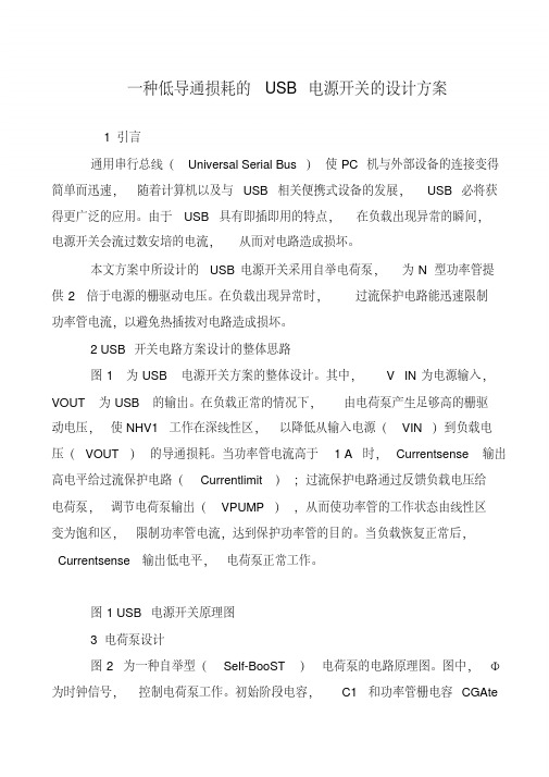
2 USB 开关电路方案设计的整体思路
图1 为USB 电源开关方案的整体设计。
其中,V IN 为电源输入,VOUT 为USB 的输出。
在负载正常的情况下,由电荷泵产生足够高的栅驱
动电压,使NHV1 工作在深线性区,以降低从输入电源(VIN )到负载电压(VOUT )的导通损耗。
当功率管电流高于 1 A 时,Currentsense 输出高电平给过流保护电路(Currentlimit ); 过流保护电路通过反馈负载电压给
电荷泵,调节电荷泵输出(VPUMP ), 从而使功率管的工作状态由线性区
变为饱和区,限制功率管电流,达到保护功率管的目的。
当负载恢复正常后,Currentsense 输出低电平,电荷泵正常工作。
图1 USB 电源开关原理图
3 电荷泵设计
图2 为一种自举型(Self-BooST )电荷泵的电路原理图。
图中,Φ为时钟信号,控制电荷泵工作。
初始阶段电容,C1 和功率管栅电容CGAte。
USB外设的电源设计

USB外设的电源设计USB(Universal Serial Bus)外设的电源设计需要考虑以下几个方面:电源供应、电源管理、电源保护等,下面将对这些方面进行详细介绍。
一、电源供应B总线供电:USB外设可以通过连接到计算机的USB接口来获取电源供应。
根据USB规范,每个USB接口的标准供电电流为500mA,即最大功率为2.5W。
因此,设计USB外设时需要确保其功耗在规定范围内,以避免对主机和其他设备造成供电不足的影响。
2.外部电源供应:如果USB外设的功耗超过了USB接口的供电能力,或者想要更加稳定和可靠的电源供应,可以考虑采用外部电源供应方式。
这种方式可以通过USB接口上的5V和GND引脚,连接外部电源适配器或电池。
设计时需要注意外部电源的电压和电流要符合USB规范,并采取电源滤波、稳压等措施来确保电源的质量和稳定性。
二、电源管理1.电源模式管理:USB外设在不同的工作状态下对电源的需求是不同的,设计时可以采用电源模式管理来实现功耗的优化。
例如,在设备处于空闲状态时可以进入低功耗模式,以减少能耗。
2.电源控制:为了进一步节省能耗,设计时可以对外设中的不同部分进行功率管理。
通过在合适的时候关闭或者降低一些模块的工作电压或频率,可以有效地减少功耗。
三、电源保护1.过压保护:设计时需要加入过压保护电路,以防止输入电压过高对外设造成损害。
可以采用过压保护芯片或者稳压芯片来监测和控制输入电压的范围。
2.过流保护:USB接口的标准供电电流为500mA,为了防止外设的过载,设计时需要考虑加入过流保护电路。
可以采用不同方案,如熔断、过流保护芯片等来实现过流保护。
3.短路保护:设计时还需要考虑加入短路保护电路,以防止外设出现短路情况时对电源或其他设备造成损害。
可以通过检测输出电流来判断是否发生短路,并及时切断电源。
4.温度保护:为了防止外设因过热而损坏,设计时可以加入温度传感器和保护电路,一旦温度超过设定阈值,及时采取措施来降低温度或者停止工作。
5V-USB开关电源充电器电路设计

5V-USB充电器电路图,有详细制作步骤文章出处: 发布时间: 2012-4-9 10:38:25 | 1958 次阅读 | 26次推荐 | 0条留言USB充电器套件,又名MP3/MP4充电器,输入AC160-240V,50/60Hz,额定输出:DC 5V 250mA (标签贴纸为500mA,如果要长期输出更大电流,请更换Q1为13003)。
MP3和MP4在全国范围大量流行,不过作为日常用品的充电器由于直接和220V高压相连,具有故障率较高,容易损坏的特点,特别是买到那些不成熟的产品后,真是苦不看言。
最后,受学校老师委托,我们联系到了一款成熟量产的充电器套件,现在一同给广大电子爱好者分享。
下面是对着实物绘制的电路原理图:(电路板上有多种元件安装方法,安装请与原理图、实物图为准,PCB板上有些元件孔是不要安装的,有些元件要装在别的元件孔上,这点请注意!)说明:为了简化电路,达到学习目地,图中用1欧的电阻F1起到保险丝的作用,用一个二极管D1完成整流作用。
接通电源后,C1会有300V左右的直流电压,通过R2给Q1的基极提供电流,Q1的发射极有R1电流检测电阻R1,Q1基极得电后,会经过T1的(3、4)产生集电极电流,并同时在T1的(5、6)(1、2)上产生感应电压,这两个次级绝缘的圈数相同的线圈,其中T1(1、2)输出由D7整流、C5滤波后通过USB座给负载供电;其中T1(5、6)经D6整流、C2滤波后通过IC1(实为4.3V稳压管)、Q2组成取样比较电路,检测输出电压高低;其中T1(5、6)、C3、R4还组成Q1三极管的正反馈电路,让Q1工作在高频振荡,不停的给T1(3、4)开关供电。
当负载变轻或者电源电压变高等任何原因导致输出电压升高时,T1(5、6)、IC1取样比较导致Q2导通,Q1基极电流减小,集电极电流减小,负载能力变小,从而导致输出电压降低;当输出电压降低后,Q2取样后又会截止,Q1的负载能力变强,输出电压又会升高;这样起到自动稳压作用。
一种USB电源开关的设计
一种USB电源开关的设计
罗翱;周泽坤;张波
【期刊名称】《微电子学》
【年(卷),期】2007(37)4
【摘要】设计了一种低导通损耗的USB电源开关电路。
该电路采用自举电荷泵为N型功率管提供足够高的栅压,以降低USB开关的导通损耗。
在过载情况下,过流保护电路能将输出电流限制在0.3 A。
【总页数】3页(P592-594)
【关键词】USB开关;自举电荷泵;N型功率管;过流保护
【作者】罗翱;周泽坤;张波
【作者单位】电子科技大学IC设计中心
【正文语种】中文
【中图分类】TN43
【相关文献】
1.一种USB电源开关的过流保护电路设计 [J], 管媛倩;官洪运
2.一种WIFI控制的电源开关的设计 [J], 蒋亚文;刘洪涛;白旭;杨雪梅;龙浩男
3.一种密码电源开关的设计 [J], 张宇驰;赵娟
4.一种基于CH9344芯片的USB转多路串口扩展设计 [J], 王子园;张勇;闫康乐
5.一种双端USB电源开关电路的设计 [J], 沈磊;倪寅凌;郑增钰
因版权原因,仅展示原文概要,查看原文内容请购买。
工程师:一款通过USB获取高效双轨电源的设计

工程师:一款通过USB获取高效双轨电源的设计
设计5V以外电源的小功率USB电路时,必须确定是使用独立电池,还是使用来自主机的小型电源。
如果电路需要大于5V的双轨电源(如采用了基于运放的仪表放大器),或必须用于便携计算机如笔记本电脑上,则问题就更复杂了。
USB2.0标准规定了对连接设备的功率要求,即耗电最大100mA,视为小功率;耗电最大500mA,则视为大功率。
本文所述电路原用于一个热致发光(TL)仪器设计,设计中的微控制器、USB接口控制器,以及10个运放均作为小功率器件,从一个USB端口获得全部电源。
设备的运行需要有高性能、低噪声拾取,使系统射频辐射尽可能低。
在搭建电路以前,做过仿真与验证,然后用于TL系统。
本设计的吸引力在于,由于它采用的是常见元器件,提高了可重复性,同时降低了成本。
图1
电路运行原理基于反激概念(图1),运行期间,一只小型变压器受一只脉冲调制555非稳电路的驱动,工作频率在115kHz~300kHz。
高工作频率可以使电路的整体尺寸较小,同时提供相对较高的功率输出以及良好的调节性,使输出滤波更容易做到低纹波。
实际电路中用一只MOSFET来实现开关。
图1中,二极管对正的VOUT。
用于手机usbotg的供电开关电源芯片设计论文
5.2.1.3寄生参数的考虑当我们用实际的工艺层次来实现电路结构、部件时,不可能避免的要引入寄生参数:寄生电阻、寄生电容、寄生PNP/NPN等等。
因此我们在绘制版图时要让引入的寄生参数对电路设计的影响降低到最低点。
要尽量减少关键电路的走线路程,因为连线会带来寄生的电阻电容。
工厂提供的寄生参数表明。
一般在金属层和多晶硅等走线时带来的寄生电容中,边缘电容占主导地位。
金属的层数越高,寄生电容越小,因此较长的金属走线可以采用高层金属,以减小布线所带来的寄生电容。
同时也要通过合理的布局,尽可能的避免版图中出现长的连线。
5.2.1.4增加冗余器件由于集成电路的平面制造工艺导致周围环境的不同,也就是说在器件的周边可能出现电场的弯曲,影响载流子的运动,宏观上造成对称使用的器件的失配:同时,也会导致重要器件的性能偏差13。
J。
对这类问题,要尽量使其周边环境相同。
在实践上,一般采用添加冗余的方法。
如图5—3是一个叉指结构的PMOS管,由6个单元组成。
两侧的分别增加了两个冗余的PMOS,它的作用就是为了使两侧的两个单元的源的掺杂情况能与其他的相同。
虽然这会造成版图面积的增大,但提高了管子的匹配度。
图5—3一个叉指结构的PM0s管扩散电阻同样存在这样的问题,也应添加冗余来减小其影响。
多晶硅电阻是通过刻蚀掺杂的多晶硅而成的,刻蚀速率一定程度上受多晶硅结构的开放性影响。
较大开放性的刻蚀速度快,因而其边沿刻蚀的较多,这造成电阻宽度较47小,电阻值较大。
这种影响也可通过添加冗余器件来减弱,如图5—4所示电阻两侧各添加了冗余电阻。
在一组多晶硅电阻两侧各添加一个冗余的电阻,其宽、长与其他电阻相同。
同时注意到,冗余多晶硅电阻两端都接地。
较不与地相连的结构,这样的结构不会有静电集聚现象,否则将影响电阻的性能。
还要提到的是,在基准源中的多晶硅电阻起重要的作用,因此,电路中的电阻都用周围都用P+注入环绕,起到隔离保护作用,避免相互问的影响。
USB外设的电源设计
( 2 )绿线为 US B +( 即D ATA+或数 据 +) ( 3 )白线为 US B- ( 即D ATA一或数据 一) ( 4 )黑线为 GND ( 地线 )
US B总线最 多支持 1 2 8 个 US B外设与计算机 系
统相 连 ,其 拓扑结构 为树形 。可 以有一个 U S B根集 线 器 ,下面还可以有若干 个集线器 ,每 个集线器可接 若干个 U S B接 口,连接 US B的线缆 , 最长不超过 5 M。 US B总线可以在 US B通道之 间动态地 分配带宽 ,这 就 大大 地提 高 了 U S B 带 宽的 利用 率 。下面 是 常 见
MO S F E T分别用作功率开关 与同步整流 。图 1 中的储
能 电 感分 成对 称 的两半 ,输 入端 的 能量 经 由跨 接于 两个 电感之间的 电容器向输 出端转移 ,这是 S E P I C电 路 的主 要特 征 。 图2 ( 见下 页 )所示 是一种设计 颇为 紧凑 的双 电 压输 出电路 ,其工作频率 为 7 5 0 kHz ,变换效率可达
用途高效 P W M 控制器 ,开关频率可 由其定时电阻端
R T的外接 电阻调 整,输 出电压则取决于反馈端 F B的 电压 采 样 分 压 器 ,外 接 的 N 沟 道 与 P 沟 道 功 率
此时 只要功 率裕量足够 ,可以首先考虑 LDO( 线性稳
压 器) ,因其成 本最低 ,所需 外 围元件也 少 ,只是 电 源效 率较低 ,不可能超过 6 7 %。若 对效率有 所要求 , 不妨 考虑 “ 电荷泵” 器件 ,因其虽在成本 与体积方面
稍逊于 L D O,但在变换效率方面 占有明显优 势。不过
此 类 器件 带 负载 能 力通 常较 弱 ,只 能满 足 低功 耗 装 置的要求 。若是需要 获取尽可能 多的有用功率 ,那 就 只能 采 用效 率更 高 的降 压型 开 关稳 压 电路 ,但 是 成
USB充电电源开关控制器

ABSOLUTE MAXIMUM RATINGS(1)
over operating free-air temperature range, voltages are referenced to GND (unless otherwise noted)
PARAMETER
MIN
MAX
UNIT
Supply voltage range
2
PRODUCTION DATA information is current as of publication date. Products conform to specifications per the terms of the Texas Instruments standard warranty. Production processing does not necessarily include testing of all parameters.
TPS2540 / 40A /41 RTE 封装及典型应用示意图
EN CTL1 CTL2 CTL3
IN 1 DM_OUT 2 DP_OUT 3 ILIM_SEL 4
ILIM0 ILIM1 GND FAULT
TPS2540/40A/41 RTE Package (Top View)
16 15 14 13
IN to OUT
-7
7
Voltage range
DP_IN, DM_IN, DP_OUT, DM_OUT
-0.3
(IN + 0.3) or 5.7
Input clamp current
DP_IN, DM_IN, DP_OUT, DM_OUT
±20
Continuous current in SDP or CDP DP_IN to DP_OUT or DM_IN to DM_OUT mode
TD9521数据手册pdf
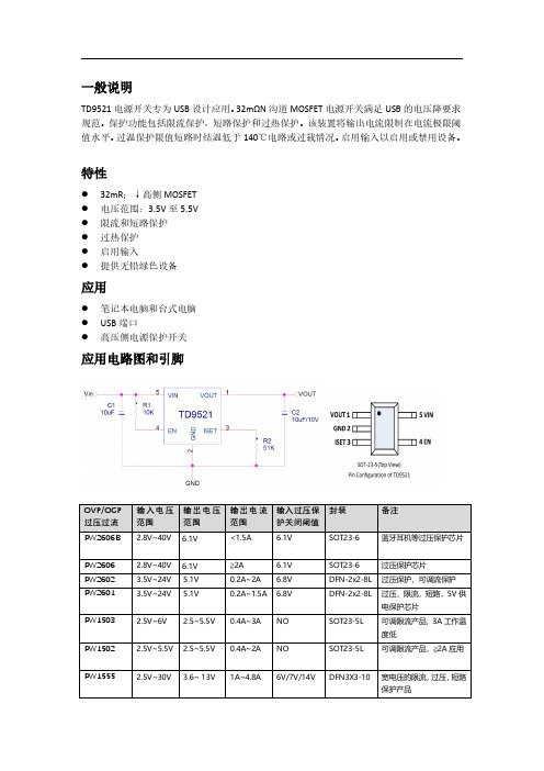
一般说明TD9521电源开关专为USB设计应用。
32mΩN沟道MOSFET电源开关满足USB的电压降要求规范。
保护功能包括限流保护,短路保护和过热保护。
该装置将输出电流限制在电流极限阈值水平。
过温保护限值短路时结温低于140℃电路或过载情况。
启用输入以启用或禁用设备。
特性⚫32mR;↓高侧MOSFET⚫电压范围:3.5V至5.5V⚫限流和短路保护⚫过热保护⚫启用输入⚫提供无铅绿色设备应用⚫笔记本电脑和台式电脑⚫USB端口⚫高压侧电源保护开关应用电路图和引脚TD9521 引脚功能描述TD9521由于价格实惠,在适合的温度下,最好的限流是2A 。
成本最低,2.4A 需要比较好的散热处理设计,3A 不建议。
PW1503在相同限流值时,具有工程师非常满意的负载温度。
在输入5V2.4A 和3A 负载限流应用时,PW1503工作温度分别在 30度和45度。
PIN 对PIN TD9521,缺点是价格高。
功能描述锁定(低电压)TD9521电源开关具有内置的欠压锁定保持输出关闭直到内部电路操作正常。
UVLO电路存在滞后和故障这样它通常会忽略输入。
当输入电压超过UVLO阈值时,输出电压启动软启动,以减少涌入电流。
电源开关电源开关是一个低RDS(开)的N沟道MOSFET。
这个内部功率MOSFET没有主体二极管。
当IC关闭时,MOSFET防止电流从VOUT流回VIN和VIN到VOUT。
限流保护TD9521电源开关提供限流保护功能。
在电流限制期间,设备将输出电流限制在电流限制阈值。
为了可靠运行,设备不应长期限流运行短路保护当输出电压低于1.5V时,这是由过载或短路时,器件会限制输出电流达到安全水平。
短路电流限制用于降低短路条件下的功耗。
如果交叉口温度达到超过温度阈值,设备将进入热关机。
伊塞特ISET引脚可以通过Riset设置电流限制:ILim=120k*1.14V/立管启用/禁用拉EN低于0.8V将禁用设备,拉EN高于2V将禁用设备启用设备。
高效USB端口电池充电设计方案
高效USB端口电池充电设计方案USB 为多种便携设备提供了通过单个“通用”电源充电的手段,从而更加方便。
但是这方面也存在着许多挑战。
以前的USB 充电能力相当有限;标准USB 主机端口的电流确实只适合为计算机外设(比如键盘,鼠标和读卡器)进行供电。
USB2.0 支持的供电电流可达500mA,可以为电池缓慢充电。
与此同时,大家期待的是如何大幅缩短充电时间。
在这个环境下,2011 年初推出的1.2 版USB 充电规范,提出了新的供电模式,增加了为设备电池充电的灵活性。
本文将介绍可支持最大1.8A 电流的专用充电接口(DCP)的概念。
这几乎是标准下行端口(SDP)USB2.0 连接承载电流的4 倍,从而能够极大加快充电时间。
关于DCPUSB 接口有4 条屏蔽线。
它们是:用于给连接外设供电的VBUS,负数据端D-,正数据端D+以及接地GND(飞特蒂亚(FTDI)公司致力于简化USB 充电,以便将开发时间、系统复杂性和工程资源的利用降低到最低限度,以获取最大的投资回报。
这样便引出了X- CHIP 系列USB 控制器IC,其主要特征是支持USB 电池充电的新概念。
每个IC 的内部电路使采用该芯片设计的便携设备能够检测到何时设备连接到了DCP。
一旦检测到DCP,X-CHIP 便在其某个CBUS 引脚上发出一个信号,启动充电。
CBUS 管脚包括BCD#、PWREN#和SLEEP#。
BCD#是漏极开路低电平有效输出信号。
它用来指示X-CHIP 何时被连接到DCP。
PWREN#是漏极开。
用于开关插座产品的USB充电部分的安全设计
用于开关插座产品的USB充电部分的安全设计Chapter 1: Introduction- Background and significance of USB charging in power socket products- Purpose and scope of the paper- Research methodology and data sourcesChapter 2: USB Charging Standards- Overview of USB charging standards, including BC1.2, Apple charging, and USB-PD- Comparison of different standards in terms of safety and compatibility- Discussion of the advantages and drawbacks of each standard Chapter 3: Safety Design Considerations- Analysis of potential safety hazards associated with USB charging in power socket products- Discussion of safety design principles, including insulation, grounding, and protection against overcurrent, overvoltage, and short circuit- Introduction to relevant safety certifications, such as UL and CE Chapter 4: Design Case Study- Presentation of a case study of a USB charging power socket product- Discussion of the product's design features related to USB charging safety- Evaluation of the product's compliance with safety standards and regulationsChapter 5: Conclusion and Future Directions- Summary of key findings and conclusions- Limitations and future research directions, including the need for further testing and evaluation of USB charging safety in power socket products.Chapter 1: IntroductionBackground and Significance of USB Charging in Power Socket Products:With the widespread use of electronic devices such as smartphones, tablets, and laptops, the demand for convenient and fast charging options has increased significantly. USB charging has emerged as a popular and versatile solution to meet this growing demand. Power socket products with built-in USB charging ports have become commonly available for use in homes, offices, and public places. However, the increasing use of USB charging in power socket products also raises concerns about safety, compatibility, and regulatory compliance.Purpose and Scope of the Paper:The purpose of this paper is to examine the USB charging standards, safety design considerations, and compliance requirements related to power socket products with USB charging ports. The paper will provide an overview of USB charging standards, compare different standards in terms of safety and compatibility, and discuss safety design principles and relevant certification requirements. The paper will also present a case study of a USB charging power socket product and evaluate its compliance with safety standards and regulations.Research Methodology and Data Sources:The research methodology for this paper involves a review of relevant literature on USB charging, safety design principles, and certification requirements. The data sources include academic articles, industry reports, and regulatory documents from organizations such as the International Electrotechnical Commission (IEC), Underwriters Laboratories (UL), and the European Committee for Electrotechnical Standardization (CENELEC). The case study evaluation will involve a review of product specifications, testing reports, and compliance documentation.Chapter 2: USB Charging StandardsOverview of USB Charging Standards:There are various USB charging standards that power socket products can support, including BC1.2, Apple charging, and USB Power Delivery (USB-PD). BC1.2 (Battery Charging 1.2) is a charging standard developed by the USB Implementers Forum (USB-IF) and is designed for charging low-power devices such as smartphones and tablets. It provides a maximum of 1.5A current at 5V voltage. Apple charging is a proprietary charging standard developed by Apple and is designed for use with Apple products. It supports higher power levels and includes Apple's proprietary communication protocol. USB-PD is a newer charging standard developed by USB-IF and is designed for higher-power devices such as laptops. It can provide up to 100W at various voltages and is capable of negotiating the optimal power delivery based on the device's requirements.Comparison of Different Standards in Terms of Safety andCompatibility:While each USB charging standard has its own specific features and benefits, they also differ in terms of safety and compatibility. BC1.2 is a well-established standard and is widely supported by devices and chargers, making it generally compatible and safe for use. Apple charging is also widely supported by Apple devices but may not be fully compatible with other devices or chargers. USB-PD is a newer standard and not yet widely supported but offers greater flexibility and higher power delivery. However, with greater power delivery comes an increased risk of safety hazards such as overcurrent, overvoltage, and short circuits.Discussion of the Advantages and Drawbacks of Each Standard: BC1.2 is a reliable and safe charging standard that is widely supported, making it a popular choice for low-power devices. However, it has limitations in power delivery capability and may not be suitable for charging higher-power devices such as laptops. Apple charging offers high power delivery and compatibility with Apple devices but may not be compatible with other devices or chargers. It also carries the risk of overcharging or overloading non-Apple devices. USB-PD offers a high degree of flexibility in power delivery and is capable of charging a range of devices with different power requirements. However, its newness and less widespread support may pose some challenges in the short term.Chapter 3: Safety Design ConsiderationsAnalysis of Potential Safety Hazards Associated with USB Charging in Power Socket Products:Power socket products with USB charging ports can pose potentialsafety hazards if not designed and manufactured with proper safety features. Overcurrent, overvoltage, and short circuits are common hazards associated with USB charging. Overcurrent can cause overheating and damage to devices, chargers, or power sockets. Overvoltage can lead to device malfunction, damage, or even fires. Short circuits can also cause fires or damage to devices and chargers.Discussion of Safety Design Principles:To minimize the risks associated with USB charging, power socket products must be designed and manufactured with proper safety features. Insulation, grounding, and overcurrent, overvoltage, and short circuit protection are essential safety design principles to consider. Insulation should be applied to prevent electrical contact with live parts and ensure user safety. Grounding is necessary to prevent electrostatic discharge and neutralize voltage differences. Overcurrent, overvoltage, and short circuit protection can detect and limit excess current, voltage, or short circuit conditions to prevent damage or fires.Introduction to Relevant Safety Certifications:Safety certification is an essential element in ensuring that power socket products with USB charging ports are safe and compliant with relevant safety regulations. Certification from organizations such as UL, CE, or CENELEC indicates that the product has been tested and evaluated for compliance with relevant safety standards. UL, for example, is a well-known third-party certification organization that provides product testing and safety evaluations for electrical products. UL certification is recognized across the industry as an important safety standard. CE is a Europeancertification that indicates compliance with relevant EU safety and environmental standards. CENELEC is a European committee that develops and publishes safety standards for electrical and electronic products.In summary, power socket products with USB charging ports can bring convenient and fast charging options to consumers. However, to ensure safety and compliance with relevant regulations, these products must be designed and manufactured with proper safety features and certified by third-party organizations such as UL, CE, or CENELEC. USB charging standards, safety design principles, and certification requirements should be carefully considered in the design and manufacturing processes of power socket products with USB charging ports.Chapter 4: Compliance Requirements Introduction to Relevant Regulations for Power Socket Products with USB Charging Ports:Power socket products with USB charging ports must comply with relevant safety regulations to ensure consumer safety and avoid legal liability. Different regions and countries have their own safety standards and certification requirements. In the US, Underwriters Laboratories (UL) certification is recognized as an important safety standard. In Europe, compliance with relevant EU safety and environmental standards is indicated by the CE marking. In addition to these regional requirements, power socket products with USB charging ports must also comply with industry-specific standards such as the IEC's International Electrotechnical Commission's standards.Analysis of Compliance Requirements for Power Socket Productswith USB Charging Ports:Compliance requirements for power socket products with USB charging ports can vary depending on several factors, such as the location of the manufacturer, the target market, and the level of power delivered by the charging port. Generally, compliance requirements for power socket products with USB charging ports include testing and certification for safety, electromagnetic compatibility (EMC), and environmental compatibility. Safety testing includes insulation resistance, electric strength, and overload testing. EMC testing involves testing for interferencewith other electronic devices and with other power socket products. Environmental testing includes resistance to temperature, humidity, and vibration.Consideration of Global Harmonization Efforts:Global harmonization efforts aim to simplify and unify safety standards and certification requirements across different regions and countries. This would make it easier for manufacturers to produce products that are compliant with multiple safety and certification standards, reducing the costs and time associated with compliance testing and certification. Significant progress has been made in global harmonization efforts through organizations such as the International Electrotechnical Commission (IEC) and the World Trade Organization (WTO). However, more work needs to be done to achieve more comprehensive global harmonization of safety standards and certification requirements.Chapter 5: Case Study: Evaluation of a USB Charging Power Socket ProductOverview of the Product:The product evaluated in this case study is a power socket with two USB charging ports rated at 2.4A each and 5VDC output. The product is intended for use in households and offices and is marketed as a convenient and safe charging solution for electronic devices such as smartphones and tablets.Evaluation of Compliance with Safety Standards and Regulations: To evaluate the compliance of the product with safety standards and regulations, the product was subjected to various tests and evaluations. These included insulation resistance, electric strength, overload, EMC, and environmental testing. The product was also evaluated for compliance with relevant safety standards such as the UL safety standard and the EU's CE marking.Insulation resistance testing showed that the product's insulation was within acceptable limits, indicating adequate protection against electric shock. Electric strength testing showed that the product could withstand a high level of voltage without breaking down, indicating adequate capacity for safety. Overload testing showed that the product could regulate current effectively, preventing overheating or damage to devices or sockets. EMC testing showed that the product did not produce significant electromagnetic interference and was not affected by interference from other electronic devices or sockets. Environmental testing showed that the product could operate within a range of temperatures and humidity levels without malfunctioning or breaking down.The product was also found to be compliant with relevant safetystandards and regulations, including the UL safety standard and the EU's CE marking. This indicates that the product has been tested and evaluated for compliance with safety, environmental, and EMC standards and is in compliance with relevant regulations. Conclusions and Recommendations:Overall, the evaluation of the USB charging power socket product showed that it was compliant with relevant safety standards and regulations and was capable of safe and effective charging of electronic devices. However, it is important to note that compliance with safety standards and regulations is not a one-time achievement but an ongoing process. Manufacturers must continuously monitor their products for compliance and adapt to changes in regulations and safety standards. In addition, manufacturers should consider global harmonization efforts to ensure that their products comply with safety standards and certification requirements in multiple regions and markets.。
4.1.3 USB 电源多功能管理方案_绿色电源——电子设备电源管理技术与解决方案_[共3页]
![4.1.3 USB 电源多功能管理方案_绿色电源——电子设备电源管理技术与解决方案_[共3页]](https://img.taocdn.com/s3/m/39c4f158cc22bcd127ff0c00.png)
绿色电源——电子设备电源管理技术与解决方案140 时,过压保护IC 应自动地再次导通。
其2.5mm × 2.5mm × 0.55mm 的超薄封装适合任何小型的便携式设计。
这种保护电路将确保移动电话通过CTTL 要求的60min 的过压测试条件。
4.1.3 USB 电源多功能管理方案充电器标准统一了,但充电解决方案还是具有差异的。
这些差别都体现在终端的内部了。
从充电器本身来看,目前仍面临着一些挑战。
① 如何高效率地管理多通道电源或负载。
② 如何在充电时使来自USB 的功率和效率最大化。
③ 如何在快速充电时实现大充电电流或较快的充电速度。
1.MAX 系列多功能充电器管理芯片MAX8662/MAX8663是MAXIM 公司推出的集成度更高的内置充电器的多功能电源管理芯片,如图4-13所示。
该系列器件内置适应USB 、AC 适配器的线性充电器以及智能电源选择器,适用于由单节可充电锂离子电池供电的便携式设备。
它内置有智能电源选择电路,可实现外部输入电源、电池以及系统负载之间的无缝分配,可用于3G 智能电话、PDA 以及其他便携式设备。
电池充电时,器件自动断开系统负载与电池的连接,并使用系统没用到的输入电源部分为电池充电,以充分利用有限的USB 电源或AC 适配器。
所有需要的功率开关和电流检测电路均集成于片上。
图4-13 MAX8662/MAX8663 的功能图充电器的输入限流值最高可调至2A ,并可支持500mA 、100mA 以及USB 挂起模式。
充电电流最高可调节至1.5A ,以适用于宽范围的电池容量。
除了充电管理外,MAX8663集成有两路高效率降压型DC/DC 变换器、四路LDO 、一个智能电源选择器及完整的充电器电路。
MAX8662提供一路升压DC/DC 变换器,可用于最多。
用于开关插座产品的USB充电部分的安全设计
用于开关插座产品的USB充电部分的安全设计
孙建龙
【期刊名称】《认证技术》
【年(卷),期】2016(000)008
【摘要】带USB充电接口的开关插座是一种在普通开关插座基础上发展而来的新型产品,其中USB充电部分的安全性能与使用者密切相关。
本文主要介绍用于开关插座的USB充电部分安全设计的总体要求、相关标准要求、关键件的选用以及安全设计的组织、管理和实施。
【总页数】3页(P62-64)
【作者】孙建龙
【作者单位】
【正文语种】中文
【相关文献】
1.NI扩展C系列产品USB-9219,USB-9229,USB-9239应用于高性能数据记录 [J], 无
2.瑞萨电子首推用于移动计算系统的USB-C Combo升降压电池充电器 [J],
3.安森美推出专用于USB充电保护的集成过压保护控制器 [J],
4.用于便携式USB装置的单片USB电源管理器、理想二极管控制器和电池充电器[J],
5.用于USB充电保护的集成过压保护控制器 [J],
因版权原因,仅展示原文概要,查看原文内容请购买。
- 1、下载文档前请自行甄别文档内容的完整性,平台不提供额外的编辑、内容补充、找答案等附加服务。
- 2、"仅部分预览"的文档,不可在线预览部分如存在完整性等问题,可反馈申请退款(可完整预览的文档不适用该条件!)。
- 3、如文档侵犯您的权益,请联系客服反馈,我们会尽快为您处理(人工客服工作时间:9:00-18:30)。
满足USB规范的电源开关设计方案
1 引言
通用串行总线(UniversalSerialBus)使PC机与外部设备的连接变得简单而迅速,随着计算机以及与USB相关便携式设备的发展,USB必将获得更广泛的应用。
由于USB具有即插即用的特点,在负载出现异常的瞬间,电源开关会流过数安培的电流,从而对电路造成损坏。
本文设计的USB电源开关采用自举电荷泵,为N型功率管提供2倍于电源的栅驱动电压。
在负载出现异常时,过流保护电路能迅速限制功率管电流,以避免热插拔对电路造成损坏。
2 USB开关电路的整体设计思路
图1为USB电源开关的整体设计。
其中,VIN为电源输入,VOUT 为USB的输出。
在负载正常的情况下,由电荷泵产生足够高的栅驱动电压,使NHV1工作在深线性区,以降低从输入电源(VIN)到负载电压(VOUT)的导通损耗。
当功率管电流高于1A时,Currentsense输出高电平。