SI3438DV-T1-E3中文资料
SI2301CDS-T1-GE3中文资料

Vishay SiliconixSi2301CDSP-Channel 20-V (D-S) MOSFET FEATURES•Halogen-free Option Available•TrenchFET ® Power MOSFETAPPLICATIONS •Load SwitchMOSFET PRODUCT SUMMARYV DS (V)R DS(on) (Ω)I D (A)a Q g (Typ.)- 200.112 at V GS = - 4.5 V - 3.1 3.3 nC0.142 at V GS = - 2.5 V- 2.7Notes:a. Based on T C = 25 °C.b. Surface Mounted on 1" x 1" FR4 board.c. t = 5 s.d. Maximum under Steady State conditions is 175 °C/W.ABSOLUTE MAXIMUM RATINGS T A = 25°C, unless otherwise notedParameter Symbol Limit U nitDrain-Source Voltage V DS - 20VGate-Source Voltage V GS ± 8Continuous Drain Current (T J = 150 °C)T C = 25 °C I D- 3.1A T C = 70 °C - 2.5T A = 25 °C - 2.3b, c T A = 70 °C - 1.8b, cPulsed Drain Current I DM - 10Continuous Source-Drain Diode CurrentT C = 25 °C I S - 1.3T A = 25 °C - 0.72b, c Maximum Power Dissipation T C = 25 °C P D 1.6WT C = 70 °C 1.0T A = 25 °C 0.86b, c T A = 70 °C 0.55b, cOperating Junction and Storage T emperature Range T J , T stg - 55 to 150°C THERMAL RESISTANCE RATINGSParameter Symbol Typical Maximum UnitMaximum Junction-to-Ambient b, d ≤ 5 s R thJA 120145°C/WMaximum Junction-to-Foot (Drain)Steady State R thJF 6278Vishay SiliconixSi2301CDSNotes:a. Pulse test; pulse width ≤ 300 µs, duty cycle ≤ 2 %.b. Guaranteed by design, not subject to production testing.Stresses beyond those listed under “Absolute Maximum Ratings” may cause permanent damage to the device. These are stress ratings only, and functional operation of the device at these or any other conditions beyond those indicated in the operational sections of the specifications is not implied. Exposure to absolute maximum rating conditions for extended periods may affect device reliability.MOSFET SPECIFICATIONS T J = 25°C, unless otherwise notedParameter Symbol Test Conditions Min.Typ.Max.U nit StaticDrain-Source Breakdown Voltage V DS V DS = 0 V, I D = - 250 µA- 20VV DS Temperature Coefficient ΔV DS /T J I D = - 250 µA - 18mV/°C V GS(th) T emperature Coefficient ΔV GS(th)/T J 2.2Gate-Source Threshold Voltage V GS(th) V DS = V GS , I D = - 250 µA - 0.4- 1V Gate-Source LeakageI GSS V DS = 0 V , V GS = ± 8 V ± 100nA Zero Gate Voltage Drain Current I DSS V DS = - 20 V , V GS = 0 V - 1µA V DS = - 20 V, V GS = 0 V , T J = 55 °C- 10On-State Drain Current aI D(on) V DS ≤ - 5 V , V GS = - 4.5 V - 6A Drain-Source On-State Resistance aR DS(on) V GS = - 4.5 V, I D = - 2.8 A 0.0900.112ΩV GS = - 2.5 V, I D = - 2.0 A 0.1100.142Forward T ransconductance a g fsV DS = - 5 V , I D = - 2.8 A2.0SDynamic bInput Capacitance C iss V DS = - 10 V , V GS = 0 V , f = 1 MHz405pFOutput CapacitanceC oss 75Reverse Transfer Capacitance C rss 55Total Gate Charge Q g V DS = - 10 V , V GS = - 4.5 V , ID = - 3 A 5.510nC V DS = - 10 V , V GS = - 2.5 V , I D = - 3 A 3.36Gate-Source Charge Q gs 0.7Gate-Drain Charge Q gd 1.3Gate Resistance R g f = 1 MHz6.0ΩTurn-On Delay Time t d(on) V DD = - 10 V, R L = 10 ΩI D = - 1 A, V GEN = - 4.5 V , R G = 1 Ω1120ns Rise Timet r 3560Turn-Off Delay Time t d(off) 3050Fall Timet f1020Drain-Source Body Diode Characteristics Continuous Source-Drain Diode Current I S T C = 25 °C- 1.3A Pulse Diode Forward Current a I SM - 10Body Diode VoltageV SD I S = - 0.7 A- 0.8- 1.2V Body Diode Reverse Recovery Time t rr I F = - 3.0 A, dI/dt = 100 A/µs, T J = 25 °C3050ns Body Diode Reverse Recovery Charge Q rr 2550nC Reverse Recovery Fall Time t a 15nsReverse Recovery Rise Timet b15Output CharacteristicsOn-Resistance vs. Drain Current and Gate VoltageTransfer CharacteristicsCapacitanceOn-Resistance vs. Junction TemperatureThreshold VoltageSingle Pulse PowerVishay SiliconixSi2301CDSTYPICAL CHARACTERISTICS 25°C, unless otherwise notedVishay Siliconix maintains worldwide manufacturing capability. Products may be manufactured at one of several qualified locations. Reliability data for Silicon Technology and Package Reliability represent a composite of all qualified locations. For related documents such as package/tape drawings, part marking, and reliability data, see /ppg?68741.Normalized Thermal Transient Impedance, Junction-to-FootDisclaimer Legal Disclaimer NoticeVishayAll product specifications and data are subject to change without notice.Vishay Intertechnology, Inc., its affiliates, agents, and employees, and all persons acting on its or their behalf (collectively, “Vishay”), disclaim any and all liability for any errors, inaccuracies or incompleteness contained herein or in any other disclosure relating to any product.Vishay disclaims any and all liability arising out of the use or application of any product described herein or of any information provided herein to the maximum extent permitted by law. The product specifications do not expand or otherwise modify Vishay’s terms and conditions of purchase, including but not limited to the warranty expressed therein, which apply to these products.No license, express or implied, by estoppel or otherwise, to any intellectual property rights is granted by this document or by any conduct of Vishay.The products shown herein are not designed for use in medical, life-saving, or life-sustaining applications unless otherwise expressly indicated. Customers using or selling Vishay products not expressly indicated for use in such applications do so entirely at their own risk and agree to fully indemnify Vishay for any damages arising or resulting from such use or sale. Please contact authorized Vishay personnel to obtain written terms and conditions regarding products designed for such applications.Product names and markings noted herein may be trademarks of their respective owners.元器件交易网。
SI3407

Vishay SiliconixSi3407DVP-Channel 20-V (D-S) MOSFETFEATURES•Halogen-free According to IEC 61249-2-21Definition•TrenchFET ® Power MOSFET •PWM Optimized •100 % R g Tested •100 % UIS Tested•Compliant to RoHS Directive 2002/95/ECPRODUCT SUMMARYV DS (V)R DS(on) (Ω)I D (A)Q g (Typ.)- 200.0240 at V GS = - 4.5 V - 8.0a 21 nC0.0372 at V GS = - 2.5 V- 8.0aNotes:a.Package limited.b.Surface Mounted on 1" x 1" FR4 board.c.t = 5 s.d.Maximum under Steady State conditions is 110 °C/W.ABSOLUTE MAXIMUM RATINGS T A = 25°C, unless otherwise notedParameter Symbol Limit UnitDrain-Source VoltageV DS - 20VGate-Source Voltage V GS± 12Continuous Drain Current (T J = 150 °C)T C = 25 °C I D - 8.0a AT C = 70 °C - 8.0aT A = 25 °C - 7.5b, c T A = 70 °C - 6.0b, cPulsed Drain Current I DM - 25Continuous Source-Drain Diode Current T C = 25 °C I S- 3.5T A = 25 °C - 1.7b, cAvalanche Current L = 0.1 mHI AS - 8Single Pulse Avalanche Energy E AS 3.2mJ Maximum Power Dissipation T C = 25 °C P D 4.2WT C = 70 °C 2.7T A = 25 °C 2.0b, c T A = 70 °C 1.3b, cOperating Junction and Storage T emperature Range T J , T stg - 55 to 150°CTHERMAL RESISTANCE RATINGSParameter Symbol Typical MaximumUnitMaximum Junction-to-Ambientb, d t ≤ 5 s R thJA 4562.5°C/WMaximum Junction-to-Foot (Drain)Steady State R thJF 2530Vishay SiliconixSi3407DVNotes:a. Pulse test; pulse width ≤ 300 µs, duty cycle ≤ 2 %.b. Guaranteed by design, not subject to production testing.Stresses beyond those listed under “Absolute Maximum Ratings” may cause permanent damage to the device. These are stress ratings only, and functional operation of the device at these or any other conditions beyond those indicated in the operational sections of the specifications is not implied. Exposure to absolute maximum rating conditions for extended periods may affect device reliability.SPECIFICATIONS T J = 25°C, unless otherwise notedParameter Symbol Test Conditions Min.Typ.Max.UnitStaticDrain-Source Breakdown Voltage V DS V GS = 0 V , I D = - 250 µA- 20V V DS Temperature Coefficient ΔV DS /T J I D = - 250 µA-18.7mV/°C V GS(th) T emperature Coefficient ΔV GS(th)/T J 3.7Gate-Source Threshold Voltage V GS(th)V DS = V GS , I D = - 250 µA - 0.65- 1.5V Gate-Source LeakageI GSS V DS = 0 V , V GS = ± 12 V ± 100nA Zero Gate Voltage Drain Current I DSS V DS = - 20 V , V GS = 0 V - 1µA V DS = - 20 V, V GS = 0 V , T J = 55 °C- 10On-State Drain Current aI D(on) V DS ≤ - 5 V, V GS = - 4.5 V - 25A Drain-Source On-State Resistance a R DS(on)V GS = - 4.5 V, I D = - 7.5 A 0.02000.0240ΩV GS = - 2.5 V, I D = - 6.4 A 0.03100.0327Forward T ransconductance a g fsV DS = - 10 V , I D = - 7.5 A25SDynamic bInput Capacitance C iss V DS = - 10 V , V GS = 0 V , f = 1 MHz1670pFOutput CapacitanceC oss 335Reverse Transfer Capacitance C rss 284Total Gate Charge Q g V DS = - 10 V , V GS = - 10 V, ID = - 7.5 A 4263nC V DS = - 10 V , V GS = - 4.5 V , I D = - 7.5 A 2132Gate-Source Charge Q gs 6Gate-Drain Charge Q gd 5Gate Resistance R g f = 1 MHz1.36.513ΩTurn-on Delay Time t d(on) V DD = - 10 V , R L = 1.7 ΩI D ≅ - 6.0 A, V GEN = - 10 V , R g = 1 Ω816ns Rise Timet r 1117Turn-Off Delay Time t d(off) 6598Fall Timet f 3959Turn-on Delay Time t d(on) V DD = - 10 V , R L = 1.7 ΩI D ≅ - 6.0 A, V GEN = - 4.5 V, R g = 1 Ω3248Rise Timet r 6293Turn-Off Delay Time t d(off) 5380Fall Timet f3857Drain-Source Body Diode Characteristics Continuous Source-Drain Diode Current I S T C = 25 °C- 3.5A Pulse Diode Forward Current a I SM - 25Body Diode VoltageV SD I S = - 6.0 A- 0.8- 1.2V Body Diode Reverse Recovery Time t rr I F = 6.0 A, dI/dt = 100 A/µs, T J = 25 °C3756ns Body Diode Reverse Recovery Charge Q rr 2233nC Reverse Recovery Fall Time t a 12nsReverse Recovery Rise Timet b25Si3407DV TYPICAL CHARACTERISTICS 25Output CharacteristicsGate ChargeTransfer CharacteristicsCapacitanceOn-Resistance vs. Junction TemperatureVishay SiliconixSi3407DVTYPICAL CHARACTERISTICS 25Source-Drain Diode Forward VoltageThreshold VoltageSafe Operating Area, Junction-to-AmbientVishay SiliconixSi3407DVTYPICAL CHARACTERISTICS 25 °C, unless otherwise noted* The power dissipation P D is based on T J(max) = 150 °C, using junction-to-case thermal resistance, and is more useful in settling the upper dissipation limit for cases where additional heatsinking is used. It is used to determine the current rating, when this rating falls below the package limit.Si3407DVVishay SiliconixTYPICAL CHARACTERISTICS 25°C, unless otherwise notedVishay Siliconix maintains worldwide manufacturing capability. Products may be manufactured at one of several qualified locations. Reliability data for Silicon Technology and Package Reliability represent a composite of all qualified locations. For related documents such as package/tape drawings, part marking, and reliability data, see /ppg?69987.Vishay SiliconixPackage InformationAN823Vishay SiliconixMounting LITTLE FOOT R TSOP-6 Power MOSFETsSurface mounted power MOSFET packaging has been based on integrated circuit and small signal packages. Those packages have been modified to provide the improvements in heat transfer required by power MOSFET s. Leadframe materials and design,molding compounds, and die attach materials have been changed. What has remained the same is the footprint of the packages.The basis of the pad design for surface mounted power MOSFET is the basic footprint for the package. For the TSOP-6 package outline drawing see /doc?71200 and see /doc?72610 for the minimum pad footprint.In converting the footprint to the pad set for a power MOSFET , you must remember that not only do you want to make electrical connection to the package, but you must made thermal connection and provide a means to draw heat from the package, and move it away from the package.In the case of the TSOP-6 package, the electrical connections are very simple. Pins 1, 2, 5, and 6 are the drain of the MOSFET and are connected together. For a small signal device or integrated circuit, typical connections would be made with traces that are 0.020 inches wide. Since the drain pins serve the additional function of providing the thermal connection to the package, this level of connection is inadequate. The total cross section of the copper may be adequate to carry the current required for the application, but it presents a large thermal impedance. Also, heat spreads in a circular fashion from the heat source. In this case the drain pins are the heat sources when looking at heat spread on the PC board.Figure 1 shows the copper spreading recommended footprint for the TSOP-6 package. This pattern shows the starting point for utilizing the board area available for the heat spreading copper. T o create this pattern, a plane of copper overlays the basic pattern on pins 1,2,5, and 6. The copper plane connects the drain pins electrically, but more importantly provides planar copper to draw heat from the drain leads and start the process of spreading the heat so it can be dissipated into the ambient air. Notice that the planar copper is shaped like a “T” to move heat away from the drain leads in all directions. This pattern uses all the available area underneath the body for this purpose.FIGURE 1. Recommended Copper Spreading Footprint0.0491.250.0100.250.1674.250.0491.25Since surface mounted packages are small, and reflow soldering is the most common form of soldering for surface mount components, “thermal” connections from the planar copper to the pads have not been used. Even if additional planar copper area is used, there should be no problems in the soldering process. The actual solder connections are defined by the solder mask openings. By combining the basic footprint with the copper plane on the drain pins, the solder mask generation occurs automatically.A final item to keep in mind is the width of the power traces. The absolute minimum power trace width must be determined by the amount of current it has to carry. For thermal reasons, this minimum width should be at least 0.020 inches. The use of wide traces connected to the drain plane provides a low impedance path for heat to move away from the device.REFLOW SOLDERINGVishay Siliconix surface-mount packages meet solder reflow reliability requirements. Devices are subjected to solder reflow as a test preconditioning and are then reliability-tested using temperature cycle, bias humidity, HAST , or pressure pot. The solder reflow temperature profile used, and the temperatures and time duration, are shown in Figures 2 and 3.Ramp-Up Rate+6_C/Second Maximum Temperature @ 155 " 15_C 120 Seconds Maximum Temperature Above 180_C 70 − 180 Seconds Maximum Temperature 240 +5/−0_C Time at Maximum Temperature20 − 40 Seconds Ramp-Down Rate+6_C/Second MaximumFIGURE 2. Solder Reflow Temperature ProfileAN823Vishay Siliconix_C/s (max)3_C/s (max)140 −THERMAL PERFORMANCEA basic measure of a device’s thermal performance is the junction-to-case thermal resistance, R q jc , or the junction-to-foot thermal resistance, R q jf . This parameter is measured for the device mounted to an infinite heat sink and is therefore a characterization of the device only, in other words, independent of the properties of the object to which the device is mounted. T able 1 shows the thermal performance of the TSOP-6.TABLE 1.Equivalent Steady State Performance—TSOP-6Thermal Resistance R q jf30_C/WSYSTEM AND ELECTRICAL IMPACT OF TSOP-6In any design, one must take into account the change in MOSFET r DS(on) with temperature (Figure 4).0.60.81.01.21.41.6−50−250255075100125150On-Resistance vs. Junction TemperatureT J − Junction Temperature (_C)FIGURE 4.Si3434DVr D S (o n ) − O n -R e s i i s t a n c e (N o r m a l i z e d )Application Note 826Vishay SiliconixP P L I C A T I O N N O T ERECOMMENDED MINIMUM PADS FOR TSOP-6Legal Disclaimer Notice VishayDisclaimerALL PRODU CT, PRODU CT SPECIFICATIONS AND DATA ARE SU BJECT TO CHANGE WITHOU T NOTICE TO IMPROVE RELIABILITY, FUNCTION OR DESIGN OR OTHERWISE.Vishay Intertechnology, Inc., its affiliates, agents, and employees, and all persons acting on its or their behalf (collectively,“Vishay”), disclaim any and all liability for any errors, inaccuracies or incompleteness contained in any datasheet or in any other disclosure relating to any product.Vishay makes no warranty, representation or guarantee regarding the suitability of the products for any particular purpose or the continuing production of any product. To the maximum extent permitted by applicable law, Vishay disclaims (i) any and all liability arising out of the application or use of any product, (ii) any and all liability, including without limitation special, consequential or incidental damages, and (iii) any and all implied warranties, including warranties of fitness for particular purpose, non-infringement and merchantability.Statements regarding the suitability of products for certain types of applications are based on Vishay’s knowledge of typical requirements that are often placed on Vishay products in generic applications. Such statements are not binding statements about the suitability of products for a particular application. It is the customer’s responsibility to validate that a particular product with the properties described in the product specification is suitable for use in a particular application. Parameters provided in datasheets and/or specifications may vary in different applications and performance may vary over time. All operating parameters, including typical parameters, must be validated for each customer application by the customer’s technical experts. Product specifications do not expand or otherwise modify Vishay’s terms and conditions of purchase, including but not limited to the warranty expressed therein.Except as expressly indicated in writing, Vishay products are not designed for use in medical, life-saving, or life-sustaining applications or for any other application in which the failure of the Vishay product could result in personal injury or death. Customers using or selling Vishay products not expressly indicated for use in such applications do so at their own risk. Please contact authorized Vishay personnel to obtain written terms and conditions regarding products designed for such applications. No license, express or implied, by estoppel or otherwise, to any intellectual property rights is granted by this document or by any conduct of Vishay. Product names and markings noted herein may be trademarks of their respective owners.Material Category PolicyVishay Intertechnology, Inc. hereby certifies that all its products that are identified as RoHS-Compliant fulfill the definitions and restrictions defined under Directive 2011/65/EU of The European Parliament and of the Council of June 8, 2011 on the restriction of the use of certain hazardous substances in electrical and electronic equipment (EEE) - recast, unless otherwise specified as non-compliant.Please note that some Vishay documentation may still make reference to RoHS Directive 2002/95/EC. We confirm that all the products identified as being compliant to Directive 2002/95/EC conform to Directive 2011/65/EU.Vishay Intertechnology, Inc. hereby certifies that all its products that are identified as Halogen-Free follow Halogen-Free requirements as per JEDEC JS709A standards. Please note that some Vishay documentation may still make reference to the IEC 61249-2-21 definition. We confirm that all the products identified as being compliant to IEC 61249-2-21 conform to JEDEC JS709A standards.Revision: 02-Oct-121Document Number: 91000。
SI4459ADY-T1-GE3;中文规格书,Datasheet资料

3600
1800 Crss
Coss
0.003 0 14 28 42 ID - Drain Current (A) 56 70
0 0 6 12 18 24 VDS - Drain-to-Source Voltage (V) 30
A
mJ
Maximum Power Dissipation
PD
W
Operating Junction and Storage Temperature Range
TJ, Tstg
°C
THERMAL RESISTANCE RATINGS
Parameter Maximum Junction-to-Ambienta, c Maximum Junction-to-Foot Notes: a. Surface mounted on 1" x 1" FR4 board. b. t = 10 s. c. Maximum under steady state conditions is 80 °C/W. d. Based on TC = 25 °C. Document Number: 69979 S11-1813-Rev. B, 12-Sep-11 This document is subject to change without notice. THE PRODUCTS DESCRIBED HEREIN AND THIS DOCUMENT ARE SUBJECT TO SPECIFIC DISCLAIMERS, SET FORTH AT /doc?91000 / 1 t 10 s Steady State Symbol RthJA RthJF Typical 29 13 Maximum 35 16 Unit °C/W
DG9431DV-T1中文资料

Vishay SiliconixDG9431Low-Voltage Single SPDT Analog SwitchFEATURES•Low Voltage Operation (+ 2.7 to + 5 V) •Low On-Resistance - r DS(on): 20 Ω•Fast Switching - t ON : 35 ns, t OFF : 20 ns •Low Leakage - I COM(on): 200-pA max •Low Charge Injection - Q INJ : 1 pC •Low Power Consumption •TTL/CMOS Compatible•ESD Protection > 2000 V (Method 3015.7) •Available in TSOP-6 and SOIC-8•Lead (Pb)-Free Version is RoHS CompliantBENEFITS•Reduced Power Consumption •Simple Logic Interface •High Accuracy•Reduce Board Space (TSOP-6)APPLICATIONS•Battery Operated Systems •Portable Test Equipment •Sample and Hold Circuits •Cellular Phones•Communication Systems •Military Radio•PBX, PABX Guidance and Control SystemsDESCRIPTIONThe DG9431 is a single-pole/double-throw monolithic CMOS analog device designed for high performance switching of analog signals. Combining low power, high speed (t ON :35ns, t OFF : 20 ns), low on-resistance (r DS(on): 20 Ω)and small physical size (TSOP-6), the DG9431 is ideal for portable and battery powered applications requiring high performance and efficient use of board space.The DG9431 is built on Vishay Siliconix’s low voltage BCD-15 process. Minimum ESD protection, per Method 3015.7, is 2000 V. An epitaxial layer prevents latchup.Break-before -make is guaranteed for DG9431.Each switch conducts equally well in both directions when on, and blocks up to the power supply level when off.As a committed partner to the community and the environment, Vishay Siliconix manufactures this product with the lead (Pb)-free device terminations. F or analog switching products manufactured with 100 % matte tin device terminations, the lead (Pb)-free “-E3” suffix is being used as a designator.FUNCTIONAL BLOCK DIAGRAM AND PIN CONFIGURATIONLogic "0" ≤ 0.8 V Logic "1" ≥ 2.4 V* Pb containing terminations are not RoHS compliant, exemptions may applyTRUTH TABLELogic NC NO 0ON OFF 1OFFONORDERING INFORMATIONTemp Range Package Part Number- 40 to 85 °CTSOP-6DG9431DV-T1DG9431DV-T1-E3 (Lead (Pb)-free)SOIC-8DG9431DY -T1DG9431DY -T1-E3 (Lead (Pb)-free)Vishay SiliconixDG9431Notes:a. Signals on S X , D X , or IN X exceeding V+ or V- will be clamped by internal diodes. Limit forward diode current to maximum current ratings.b. All leads welded or soldered to PC Board.c. Derate 6.5 mW/°C above 75 °C.ABSOLUTE MAXIMUM RATINGSParameterLimit Unit Reference V+ to GND- 0.3 to + 13V IN, COM, NC, NO a- 0.3 to (V+ + 0.3)Continuous Current (Any Terminal)± 20mA Peak Current (Pulsed at 1 ms, 10 % duty cycle)± 40ESD (Method 3015.7)> 2000V Storage T emperature (D Suffix)- 65 to 125°C Power Dissipation (Packages)b8-Pin Narrow Body SOIC c400mWSPECIFICATIONS (V+ = 3 V)Parameter Symbol Test ConditionsUnless Otherwise Specified V+ = 3 V , ± 10 %, V IN = 0.8 or 2.4 V e Temp aD Suffix - 40 to 85 °CUnitMin cTyp bMax cAnalog Switch Analog Signal Range d V ANALOG Full 03VDrain-Source On–Resistance r DS(on)V NO or V NC = 1.5 V, V+ = 2.7 VI COM = 5 mARoom Full 305080Ωr DS(on)Match d Δr DS(on)V NO or V NC = 1.5 V Room 0.42r DS(on) Flatness fr DS(on)Flatness V NO or V NC = 1 and 2 VRoom 48NO or NC Off Leakage Current gI NO/NC(off)V NO or V NC = 1 V/2 V , V COM = 2 V/1 V Room Full - 100- 500051005000pA COM Off Leakage Current g I COM(off)V COM = 1 V/2 V, V NO or V NC = 2 V/1 VRoom Full - 100- 500051005000Channel-On Leakage Current g I COM(on)V COM = V NO or V NC = 1 V/2 VRoom Full- 200- 100001020010000Digital Control Input CurrentI INL or I INHFull1µADynamic Characteristics Turn-On Time t ON V NO or V NC = 1.5 VRoomFull 50120200nsTurn-Off Timet OFF Room Full 2050120Break-Before-Make Time t d Room 320Charge Injection Q INJ C L = 1 nF , V gen = 0 V, R gen = 0 ΩRoom 15pC Off-IsolationOIRR R L = 50 Ω, C L = 5 pF , f = 1 MHzRoom - 74dB Source Off Capacitance C S(off) f = 1 MHz Room 7pFChannel-On Capacitance C D(on)Room32Power Supply Power Supply Range V+ 2.712V Power Supply CurrentI+V+ = 3.3 V , V IN = 0 or 3.3 V1µAVishay SiliconixDG9431Notes:a. Room = 25 °C, Full = as determined by the operating suffix.b. Typical values are for design aid only, not guaranteed nor subject to production testing.c. The algebraic convention whereby the most negative value is a minimum and the most positive a maximum, is used in this data sheet.d. Guarantee by design, nor subjected to production test.e. V IN = input voltage to perform proper function.f. Difference of min and max values.g. Guraranteed by 5-V leakage testing, not production tested.Stresses beyond those listed under “Absolute Maximum Ratings” may cause permanent damage to the device. These are stress ratings only, and functional operation of the device at these or any other conditions beyond those indicated in the operational sections of the specifications is not implied. Exposure to absolute maximum rating conditions for extended periods may affect device reliability.SPECIFICATIONS (V+ = 5 V)Parameter Symbol Test ConditionsUnless Otherwise Specified V+ = 5 V , ± 10 %, V IN = 0.8 or 2.4 V e Temp aD Suffix - 40 to 85 °CUnitMin cTyp bMax cAnalog Switch Analog Signal Range d V ANALOG Full 05VDrain-Source On–Resistance r DS(on)V NO or V NC = 3.5 V , V+ = 4.5 VI COM = 5 mARoom Full 203050Ωr DS(on)Match d Δr DS(on)V NO or V NC = 1.5 V Room 0.42r DS(on) Flatness fr DS(on)Flatness V NO or V NC = 1, 2 and 3 V Room 26NO or NC Off Leakage Current I NO/NC(off)V NO or V NC = 1 V/4 V , V COM = 4 V/1 V Room Full - 100- 5000101005000pA COM Off Leakage Current I COM(off)V COM = 1 V/4 V , V NO or V NC = 4 V/1 VRoom Full - 100- 5000101005000Channel-On Leakage Current I COM(on)V COM = V NO or V NC = 1 V/4 VRoom Full- 200- 1000020010000Digital Control Input CurrentI INL or I INHFull1µADynamic Characteristics T urn-On Time t ON V NO or V NC = 3.0 VRoomFull 3575150nsT urn-Off Timet OFF Room Full 2050100Break-Before-Make Time t d Room 310Charge Injection Q INJ C L = 1 nF , V gen = 0 V , R gen = 0 ΩRoom 25pC Off-IsolationOIRR R L = 50 Ω, C L = 5 pF , f = 1 MHzRoom - 74dB NC and NO Capacitance C (off) f = 1 MHz Room - 7pFChannel-On Capacitance C D(on)Room32Power Supply Power Supply Range V+ 2.712V Power Supply CurrentI+V+ = 5.5 V , V IN = 0 or 5.5 V1µAVishay SiliconixDG9431TYPICAL CHARACTERISTICS 25 °C, unless otherwise notedLeakage Current vs. TemperatureIN Off-Isolation vs. Frequencyr DS vs. VCOMVishay SiliconixDG9431TYPICAL CHARACTERISTICS 25 °C, unless otherwise notedDS COMt ON /t OFF vs. Power Supply VoltageSwitching Time vs. TemperatureDG9431Vishay SiliconixTEST CIRCUITSFigure 1. Switching TimeFigure 2. Break-Before-Make IntervalFigure 3. Charge InjectionVishay SiliconixDG9431TEST CIRCUITSVishay Siliconix maintains worldwide manufacturing capability. Products may be manufactured at one of several qualified locations. Reliability data for Silicon Tech-nology and Package Reliability represent a composite of all qualified locations. For related documents such as package/tape drawings, part marking, and reliability data, see /ppg?70831.Figure 4. Off-IsolationFigure 5. Channel Off/On CapacitanceDisclaimer Legal Disclaimer NoticeVishayAll product specifications and data are subject to change without notice.Vishay Intertechnology, Inc., its affiliates, agents, and employees, and all persons acting on its or their behalf (collectively, “Vishay”), disclaim any and all liability for any errors, inaccuracies or incompleteness contained herein or in any other disclosure relating to any product.Vishay disclaims any and all liability arising out of the use or application of any product described herein or of any information provided herein to the maximum extent permitted by law. The product specifications do not expand or otherwise modify Vishay’s terms and conditions of purchase, including but not limited to the warranty expressed therein, which apply to these products.No license, express or implied, by estoppel or otherwise, to any intellectual property rights is granted by this document or by any conduct of Vishay.The products shown herein are not designed for use in medical, life-saving, or life-sustaining applications unless otherwise expressly indicated. Customers using or selling Vishay products not expressly indicated for use in such applications do so entirely at their own risk and agree to fully indemnify Vishay for any damages arising or resulting from such use or sale. Please contact authorized Vishay personnel to obtain written terms and conditions regarding products designed for such applications.Product names and markings noted herein may be trademarks of their respective owners.元器件交易网。
SI1555DL-T1-E3中文资料

FEATURESD TrenchFET rPower MOSFETPb-free AvailableSi1555DLVishay SiliconixDocument Number: 71079S-50245—Rev. D, 21-Feb-051Complementary Low-Threshold MOSFET PairPRODUCT SUMMARYV DS (V)r DS(on) (W )I D (A)0.385 @ V GS = 4.5 V 0.70N-Channel200.630 @ V GS = 2.5 V 0.540.600 @ V GS = −4.5 V −0.60P-Channel −80.850 @ V GS = −2.5 V −0.501.200 @ V GS = −1.8 V−0.42Marking CodeRBXXLot Traceability and Date CodePart # Code Y YOrdering Information:Si1555DL-T1Si1555DL-T1—E3 (Lead (Pb)-Free)SOT-363SC-70 (6-LEADS)Top ViewS 1G 1D 2D 1G 2S 2ABSOLUTE MAXIMUM RATINGS (T A = 25_C UNLESS OTHERWISE NOTED)N-ChannelP-Channel ParameterSymbol5 secs Steady State5 secsSteady StateUnitDrain-Source Voltage V DS 20−8Gate-Source VoltageV GS "12"8VT A = 25_C "0.70"0.66−0.60−0.57Continuous Drain Current (T J = 150_C)a T A = 85_CI D "0.50"0.48−0.43−0.41Pulsed Drain CurrentI DM "1.0AContinuous Source Current (Diode Conduction)a I S 0.250.23−0.25−0.23Maximum Power Dissipation T A = 25_C 0.300.270.300.27aT A = 85_C P D 0.160.140.160.14W Operating Junction and Storage Temperature RangeT J , T stg−55 to 150_CTHERMAL RESISTANCE RATINGSParameterSymbol TypicalMaximumUnitM iJ ti t A bi t t v 5 sec 360415Maximum Junction-to-Ambient a Steady State R thJA 400460_Maximum Junction-to-Foot (Drain)Steady StateR thJF300350C/WNotesa.Surface Mounted on 1” x 1” FR4 Board.Si1555DLVishay Siliconix2Document Number: 71079S-50245—Rev. D, 21-Feb-05SPECIFICATIONS (T J = 25_C UNLESS OTHERWISE NOTED)ParameterSymbol Test Condition Min Typ Max UnitStaticV DS = V GS , I D = 250 m A N-Ch 0.6 1.4Gate Threshold VoltageV GS(th)V DS = V GS , I D = −250 m A P-Ch −0.45−1.0VGate Body Leakage V DS = 0 V, V GS = "12 V N-Ch "100Gate-Body LeakageI GSSV DS = 0 V, V GS = "8 V P-Ch "100nAV DS = 20 V, V GS = 0 VN-Ch 1V DS = −8 V, V GS = 0 V P-Ch −1Zero Gate Voltage Drain CurrentI DSSV DS = 20 V, V GS = 0 V, T J = 85_C N-Ch 5m A V DS = −8 V, V GS = 0 V, T J = 85_CP-Ch −5On State Drain Current D()V DS w 5 V, V GS = 4.5 V N-Ch 1.0On-State Drain Current aI D(on)V DS p −5 V, V GS = −4.5 V P-Ch −1.0A V GS = 4.5 V, I D = 0.66 A N-Ch 0.3200.385V GS = −4.5 V, I D = −0.57 AP-Ch 0.5100.600Drain-Source On-State Resistance ar V GS = 2.5 V, I D = 0.40 A N-Ch 0.5600.630WDS(on)V GS = −2.5 V, I D = −0.48 A P-Ch 0.7200.850V GS = −1.8 V, I D = −0.20 AP-Ch 1.00 1.200Forward Transconductance f V DS = 10 V, I D = 0.66 A N-Ch 1.5ag fs V DS = −4 V, I D = −0.57 A P-Ch 1.2S Diode Forward Voltage I S = 0.23 A, V GS = 0 V N-Ch 0.8 1.2a V SDI S = −0.23 A, V GS = 0 VP-Ch−0.8−1.2VDynamic bN-Ch 0.8 1.2Total Gate ChargeQ gN-ChannelP-Ch 1.5 2.3Gate Source Charge V DS = 10 V, V GS = 4.5 V, I D = 0.66 A N-Ch 0.06Gate-Source ChargeQ gs P-Channel4 V 45 V I 057 AP-Ch 0.17nCGate Drain Charge d V DS = −4 V, V GS = −4.5 V, I D = −0.57 A N-Ch 0.30Gate-Drain ChargeQ gd P-Ch 0.16Turn On Delay Time d()N-Ch 1020Turn-On Delay Timet d(on)P-Ch612N-ChannelN-Ch 1630Rise Timet r V DD = 10 V, R L = 20 WI D ^ 0.5 A, V GEN = 4.5 V, R = 6 W P-Ch 2550Turn Off Delay Time d(ff)g P-Channel V 4 V R 8 WN-Ch 1020Turn-Off Delay Timet d(off)DD = −4 V, R L = 8 I −0.5 A, V −4.5 V, R P-Ch 1020nsD ^ GEN = g = 6 WN-Ch 1020Fall Timet f P-Ch1020Source-DrainI F = 0.23 A, di/dt = 100 A/m s N-Ch 2040Reverse Recovery Timet rrI F = −0.23 A, di/dt = 100 A/m sP-Ch2040Notesa.Pulse test; pulse width v 300 m s, duty cycle v 2%.b.Guaranteed by design, not subject to production testing.Stresses beyond those listed under “Absolute Maximum Ratings” may cause permanent damage to the device. These are stress ratings only, and functional operation of the device at these or any other conditions beyond those indicated in the operational sections of the specifications is not implied. Exposure to absolute maximum rating conditions for extended periods may affect device reliability.Si1555DLVishay SiliconixDocument Number: 71079S-50245—Rev. D, 21-Feb-0530.00.5 1.0 1.5 2.0 2.50.00.51.01.52.02.53.0V DS − Drain-to-Source Voltage (V)V GS − Gate-to-Source Voltage (V)2040608010048121620− O n -R e s i s t a n c e (r D S (o n )W )0.60.81.01.21.41.6−50−2502550751001251500123450.00.20.40.60.80.00.20.40.60.81.00.00.20.40.60.81.0V DS − Drain-to-Source Voltage (V)On-Resistance vs. Drain Current− G a t e -t o -S o u r c e V o l t a g e (V )Q g − Total Gate Charge (nC)C − C a p a c i t a n c e (p F )V G S CapacitanceOn-Resistance vs. Junction TemperatureT J − Junction Temperature (_C)r D S (o n ) − O n -R e s i i s t a n c e (N o r m a l i z e d )Si1555DLVishay Siliconix4Document Number: 71079S-50245—Rev. D, 21-Feb-05TYPICAL CHARACTERISTICS (25_C UNLESS NOTED)N−CHANNEL0.00.20.40.60.81.01.20.00.20.40.60.81.01234510.1− O n -R e s i s t a n c e (r D S (o n )W )V SD − Source-to-Drain Voltage (V)V GS − Gate-to-Source Voltage (V)− S o u r c e C u r r e n t (A )I S 03512P o w e r (W )Single Pulse PowerTime (sec)411006001010−110−210−3−0.4−0.3−0.2−0.1−0.00.10.2−50−250255075100125150210.10.01Threshold VoltageV a r i a n c e (V )V G S (t h )T J − Temperature (_C)Normalized Thermal Transient Impedance, Junction-to-AmbientSquare Wave Pulse Duration (sec)N o r m a l i z e d E f f e c t i v e T r a n s i e n t T h e r m a l I m p e d a n c eSi1555DLVishay SiliconixDocument Number: 71079S-50245—Rev. D, 21-Feb-055TYPICAL CHARACTERISTICS (25_C UNLESS NOTED)N−CHANNEL10−310−211010−110−4210.10.01Normalized Thermal Transient Impedance, Junction-to-FootSquare Wave Pulse Duration (sec)N o r m a l i z e d E f f e c t i v e T r a n s i e n t T h e r m a l I m p e d a n c e0.00.5 1.0 1.5 2.0 2.5V GS − Gate-to-Source Voltage (V)40801201602468− O n -R e s i s t a n c e (r D S (o n )W )0.00.51.01.52.00.00.20.40.60.81.0V DS − Drain-to-Source Voltage (V)I D − Drain Current (A)C − C a p a c i t a n c e (p F )CapacitanceSi1555DLVishay Siliconix6Document Number: 71079S-50245—Rev. D, 21-Feb-050.00.20.40.60.8 1.0 1.2 1.4 1.6Q g − Total Gate Charge (nC)0.00.20.40.60.81.01.20.00.51.01.52.01234510.1− O n -R e s i s t a n c e (r D S (o n )W )V SD − Source-to-Drain Voltage (V)V GS − Gate-to-Source Voltage (V)− S o u r c e C u r r e n t (A )I S 03512P o w e r (W )Single Pulse PowerTime (sec)411006001010−110−210−3−0.2−0.10.00.10.20.30.4−50−250255075100125150Threshold VoltageV a r i a n c e (V )V G S (t h )T J − Temperature (_C)Si1555DLVishay SiliconixDocument Number: 71079S-50245—Rev. D, 21-Feb-057TYPICAL CHARACTERISTICS (25_C UNLESS NOTED)P−CHANNEL210.10.01Normalized Thermal Transient Impedance, Junction-to-AmbientSquare Wave Pulse Duration (sec)N o r m a l i z e d E f f e c t i v e T r a n s i e n t T h e r m a l I m p e d a n c e10−310−211010−110−4210.10.01Normalized Thermal Transient Impedance, Junction-to-FootSquare Wave Pulse Duration (sec)N o r m a l i z e d E f f e c t i v e T r a n s i e n t T h e r m a l I m p e d a n c eVishay Siliconix maintains worldwide manufacturing capability. Products may be manufactured at one of several qualified locations. Reliability data for Silicon T echnology and Package Reliability represent a composite of all qualified locations. For related documents such as package/tape drawings, part marking, and reliability data, see /ppg?71079.Document Number: 91000Revision: 18-Jul-081DisclaimerLegal Disclaimer NoticeVishayAll product specifications and data are subject to change without notice.Vishay Intertechnology, Inc., its affiliates, agents, and employees, and all persons acting on its or their behalf (collectively, “Vishay”), disclaim any and all liability for any errors, inaccuracies or incompleteness contained herein or in any other disclosure relating to any product.Vishay disclaims any and all liability arising out of the use or application of any product described herein or of any information provided herein to the maximum extent permitted by law. The product specifications do not expand or otherwise modify Vishay’s terms and conditions of purchase, including but not limited to the warranty expressed therein, which apply to these products.No license, express or implied, by estoppel or otherwise, to any intellectual property rights is granted by this document or by any conduct of Vishay.The products shown herein are not designed for use in medical, life-saving, or life-sustaining applications unless otherwise expressly indicated. Customers using or selling Vishay products not expressly indicated for use in such applications do so entirely at their own risk and agree to fully indemnify Vishay for any damages arising or resulting from such use or sale. Please contact authorized Vishay personnel to obtain written terms and conditions regarding products designed for such applications.Product names and markings noted herein may be trademarks of their respective owners.元器件交易网。
MC3440DV规格书

These miniature surface mount MOSFETs utilize a high cell density trench process to provide low r DS(on)and to ensure minimal power loss and heat dissipation. Typical applications are DC-DCconverters and power management in portable and battery-powered products such as computers, printers, PCMCIA cards, cellular and cordless telephones.V DS (V)r DS(on) (Ω)I D (A)0.700 @ V GS = 10 V1.11.200 @ V GS = 5.5V0.8PRODUCT SUMMARY 150N-Channel 150V (D-S) MOSFET•Low r DS(on)provides higher efficiency and extends battery life•Low thermal impedance copper leadframe TSOP-6 saves board space •Fast switching speed•High performance trench technologyNotes a.Surface Mounted on 1” x 1” FR4 Board.b.Pulse width limited by maximum junction temperatureSymbol Maximum UnitsV DS 150V GS ±20Continuous Drain Current aT A =25oC I D1.1I DM ±10I S1.1A Power DissipationaT A =25oC P D1.15WT J , T stg -55 to 150oCOperating Junction and Storage Temperature Range Continuous Source Current (Diode Conduction)aABSOLUTE MAXIMUM RATINGS (T A = 25 oC UNLESS OTHERWISE NOTED)Parameter Pulsed Drain Current bVGate-Source Voltage Drain-Source VoltageA SymbolTypMaxt <= 10 sec 93110Steady State130150THERMAL RESISTANCE RATINGSMaximum Junction-to-Ambient aoC/WR thJAParameterTSOP-6Top ViewD D SD D G123654D 1S 1G 1N-Channel MOSFETNotes a.Pulse test: PW <= 300us duty cycle <= 2%.b.Guaranteed by design, not subject to production testing.Min Typ MaxGate-Threshold Voltage V GS(th)V DS = V GS , I D = 250 uA1.0V Gate-Body LeakageI GSS V DS = 0 V, V GS = ±8 V±100nA V DS = 120 V, V GS = 0 V1V DS = 120 V, V GS = 0 V, T J = 55oC10On-State Drain CurrentAI D(on)V DS = 5 V, V GS = 10 V 10AV GS = 10 V, I D = 1.1 A 700V GS = 5.5 V, I D = 0.8 A 1200Forward Tranconductance Ag fs V DS = 10 V, I D = 1.1 A 11.3S Diode Forward VoltageV SD I S = 1.6 A, V GS = 0 V0.75VTotal Gate Charge Q g 7.0Gate-Source Charge Q gs 1.1Gate-Drain Charge Q gd 2.0Turn-On Delay Time t d(on)8Rise Timet r 24Turn-Off Delay Time t d(off)35Fall-Timet f10m ΩParameterLimitsUnitV DD = 10 V, R L = 15 Ω, I D = 1 A,V GEN = 4.5 VV DS = 10 V, V GS = 5.5 V, I D = 1.1 A nCnsDynamicbSPECIFICATIONS (T A = 25oC UNLESS OTHERWISE NOTED)uA I DSS Zero Gate Voltage Drain Current StaticTest ConditionsSymbol Drain-Source On-Resistance Ar DS(on)FREESCALE reserves the right to make changes without further notic e to any products herein. freescale makes no warranty, representation or guarantee regarding the suitability of its products for any particular purpose, nor does freescale assume any liability arising ou t of the application or use of any product or circuit, and specifically disclaims any and all liability, including without limitation special, consequential or incidentaldamages. “Typical” parameters which may be provided in freescale data sheet s and/or specifications can and do vary in different applications and actual performance may vary over time. All operating parameters, including “Typicals” must be validated for each customer application bycustomer’s technical experts. freescale does not convey any license under its patent rights nor the rights of others. freescale products are not designed, intended, or authorized for use as components in systems intended for surgical implant into the body, or other applications intended to support or sustain life, or for any other application in which the failure of the freescale product could create a situation where personal injury or death may occur. Should Buyer purchase or use freescale products for any such uninte nded or unauthorized application, Buyer shall indemnify and hold freescale and its officers, employees, subsidiaries, affiliates, and distributors harmless against all claims, costs, damages, and expenses, and reasonable attorney fees arising out of, directly or indirectly, any claim of personal injury or death associated with such unintended or unauthorized use, even if such claim alleges that freescale was negligent regarding the design or m anufacture of the part. freescale is an Equal Opportunity/Affirmative Action Employer.Package Information TSOP-6: 6LEAD。
SI3407DV中文资料

Vishay SiliconixSi3407DVP-Channel 20-V (D-S) MOSFETFEATURES•TrenchFET ® Power MOSFET •PWM Optimized •100 % R g Tested •100 % UIS TestedAPPLICATIONS•Load SwitchPRODUCT SUMMARYV DS (V)R DS(on) (Ω)I D (A)Q g (Typ.)- 200.0240 at V GS = - 4.5 V - 8.0a 21 nC0.0372 at V GS = - 2.5 V- 8.0aNotes:a.Package limited.b.Surface Mounted on 1" x 1" FR4 board.c.t = 5 s.d.Maximum under Steady State conditions is 110 °C/W.ABSOLUTE MAXIMUM RATINGS T A = 25°C, unless otherwise notedParameter Symbol Limit UnitDrain-Source VoltageV DS - 20VGate-Source Voltage V GS± 12Continuous Drain Current (T J = 150 °C)T C = 25 °C I D - 8.0a ATC = 70 °C - 8.0aT A = 25 °C - 7.5b, c T A = 70 °C - 6.0b, cPulsed Drain Current I DM - 25Continuous Source-Drain Diode Current T C = 25 °C I S- 3.5T A = 25 °C - 1.7b, cAvalanche Current L = 0.1 mHI AS - 8Single Pulse Avalanche Energy E AS 3.2mJ Maximum Power Dissipation T C = 25 °C P D 4.2WT C = 70 °C 2.7T A = 25 °C 2.0b, c T A = 70 °C 1.3b, cOperating Junction and Storage T emperature Range T J , T stg - 55 to 150°CTHERMAL RESISTANCE RATINGSParameter Symbol Typical MaximumUnitMaximum Junction-to-Ambientb, d t ≤ 5 s R thJA 4562.5°C/WMaximum Junction-to-Foot (Drain)Steady State R thJF 2530Vishay SiliconixSi3407DVNotes:a. Pulse test; pulse width ≤ 300 µs, duty cycle ≤ 2 %.b. Guaranteed by design, not subject to production testing.Stresses beyond those listed under “Absolute Maximum Ratings” may cause permanent damage to the device. These are stress ratings only, and functional operation of the device at these or any other conditions beyond those indicated in the operational sections of the specifications is not implied. Exposure to absolute maximum rating conditions for extended periods may affect device reliability.SPECIFICATIONS T J = 25°C, unless otherwise notedParameter S ymbol Test Conditions Min.Typ.Max.UnitStaticDrain-Source Breakdown Voltage V DS V GS = 0 V , I D = - 250 µA- 20V V DS Temperature Coefficient ΔV DS /T J I D = - 250 µA-18.7mV/°C V GS(th) T emperature Coefficient ΔV GS(th)/T J 3.7Gate-Source Threshold Voltage V GS(th)V DS = V GS , I D = - 250 µA - 0.65- 1.5V Gate-Source LeakageI GSS V DS = 0 V , V GS = ± 12 V ± 100nA Zero Gate Voltage Drain Current I DSS V DS = - 20 V , V GS = 0 V - 1µA V DS = - 20 V, V GS = 0 V , T J = 55 °C- 10On-State Drain Current aI D(on) V DS ≤ - 5 V, V GS = - 4.5 V - 25A Drain-Source On-State Resistance a R DS(on)V GS = - 4.5 V, I D = - 7.5 A 0.02000.0240ΩV GS = - 2.5 V, I D = - 6.4 A 0.03100.0327Forward T ransconductance a g fsV DS = - 10 V , I D = - 7.5 A25SDynamic bInput Capacitance C iss V DS = - 10 V , V GS = 0 V , f = 1 MHz1670pFOutput CapacitanceC oss 335Reverse Transfer Capacitance C rss 284Total Gate Charge Q g V DS = - 10 V , V GS = - 10 V, ID = - 7.5 A 4263nC V DS = - 10 V , V GS = - 4.5 V , I D = - 7.5 A 2132Gate-Source Charge Q gs 6Gate-Drain Charge Q gd 5Gate Resistance R g f = 1 MHz1.36.513ΩTurn-on Delay Time t d(on) V DD = - 10 V , R L = 1.7 ΩI D ≅ - 6.0 A, V GEN = - 10 V , R g = 1 Ω816ns Rise Time t r 1117Turn-Off Delay Timet d(off) 6598Fall Timet f 3959Turn-on Delay Time t d(on) V DD = - 10 V , R L = 1.7 ΩI D ≅ - 6.0 A, V GEN = - 4.5 V, R g = 1 Ω3248Rise Timet r 6293Turn-Off Delay Time t d(off) 5380Fall Timet f3857Drain-Source Body Diode Characteristics Continuous Source-Drain Diode Current I S T C = 25 °C- 3.5A Pulse Diode Forward Current a I SM - 25Body Diode VoltageV SD I S = - 6.0 A- 0.8- 1.2V Body Diode Reverse Recovery Time t rr I F = 6.0 A, di/dt = 100 A/µs, T J = 25 °C3756ns Body Diode Reverse Recovery Charge Q rr 2233nC Reverse Recovery Fall Time t a 12nsReverse Recovery Rise Timet b25Si3407DV TYPICAL CHARACTERISTICS 25Output CharacteristicsGate ChargeTransfer CharacteristicsCapacitanceOn-Resistance vs. Junction TemperatureVishay SiliconixSi3407DVTYPICAL CHARACTERISTICS 25Source-Drain Diode Forward VoltageThreshold VoltageSafe Operating Area, Junction-to-AmbientVishay SiliconixSi3407DVTYPICAL CHARACTERISTICS 25 °C, unless otherwise noted* The power dissipation P D is based on T J(max) = 150 °C, using junction-to-case thermal resistance, and is more useful in settling the upper dissipation limit for cases where additional heatsinking is used. It is used to determine the current rating, when this rating falls below the package limit.Vishay SiliconixSi3407DVTYPICAL CHARACTERISTICS 25°C, unless otherwise notedVishay Silicon ix main tain s worldwide man ufacturin g capability. Products may be man ufactured at on e of several qualified location s. Reliability data for Silicon Technology and Package Reliability represent a composite of all qualified locations. For related documents such as package/tape drawings, part marking, and reliability data, see /ppg?69987.Disclaimer Legal Disclaimer NoticeVishayAll product specifications and data are subject to change without notice.Vishay Intertechnology, Inc., its affiliates, agents, and employees, and all persons acting on its or their behalf (collectively, “Vishay”), disclaim any and all liability for any errors, inaccuracies or incompleteness contained herein or in any other disclosure relating to any product.Vishay disclaims any and all liability arising out of the use or application of any product described herein or of any information provided herein to the maximum extent permitted by law. The product specifications do not expand or otherwise modify Vishay’s terms and conditions of purchase, including but not limited to the warranty expressed therein, which apply to these products.No license, express or implied, by estoppel or otherwise, to any intellectual property rights is granted by this document or by any conduct of Vishay.The products shown herein are not designed for use in medical, life-saving, or life-sustaining applications unless otherwise expressly indicated. Customers using or selling Vishay products not expressly indicated for use in such applications do so entirely at their own risk and agree to fully indemnify Vishay for any damages arising or resulting from such use or sale. Please contact authorized Vishay personnel to obtain written terms and conditions regarding products designed for such applications.Product names and markings noted herein may be trademarks of their respective owners.元器件交易网。
SI3948DV-T1-GE3;中文规格书,Datasheet资料

Vishay SiliconixSi3948DVDual N-Channel 30-V (D-S) MOSFETFEATURES•Halogen-free According to IEC 61249-2-21Definition•TrenchFET ® Power MOSFETs•Compliant to RoHS Directive 2002/95/ECPRODUCT SUMMARYV DS (V)R DS(on) (Ω)I D (A)300.105 at V GS = 10 V ± 2.50.175 at V GS = 4.5 V± 2.0Notes:a. Surface Mounted on FR4 board.b. t ≤ 5 s.ABSOLUTE MAXIMUM RATINGS T A = 25 °C, unless otherwise notedParameter Symbol Limit UnitDrain-Source Voltage V DS 30VGate-Source VoltageV GS ± 20Continuous Drain Current (T J = 150 °C)a, b T A = 25 °C I D ± 2.5A T A = 70 °C± 2.0Pulsed Drain Current (10 µs Pulse Width)I DM ± 8Continuous Source Current (Diode Conduction)a, b I S 1.05Maximum Power Dissipation a, bT A = 25 °C P D 1.15W T A = 70 °C 0.73Operating Junction and Storage T emperature RangeT J , T stg- 55 to 150°C THERMAL RESISTANCE RATINGSParameter Symbol T ypical Maximum UnitMaximum Junction-to-Ambient a t ≤ 5 s R thJA 93110°C/WSteady State 130150Maximum Junction-to-Lead Steady StateR thJL7590Vishay SiliconixSi3948DVNotes:a. Pulse test; pulse width ≤ 300 µs, duty cycle ≤ 2 %.b. Guaranteed by design, not subject to production testing.Stresses beyond those listed under “Absolute Maximum Ratings” may cause permanent damage to the device. These are stress ratings only, and functional operation of the device at these or any other conditions beyond those indicated in the operational sections of the specifications is not implied. Exposure to absolute maximum rating conditions for extended periods may affect device reliability.SPECIFICATIONS T J = 25 °C, unless otherwise notedParameter Symbol T est Conditions Min.T yp.Max.UnitStaticGate Threshold Voltage V GS(th) V DS = V GS , I D = 250 µA 1.0VGate-Body LeakageI GSS V DS = 0 V , V GS = ± 20 V ± 100 nAZero Gate Voltage Drain Current I DSS V DS = 24 V, V GS = 0 V 1µA V DS = 24 V , V GS = 0 V , T J = 55 °C5On-State Drain Current aI D(on) V DS ≥ 5 V , V GS = 10 V 5A Drain-Source On-State Resistance a R DS(on) V GS = 10 V, I D = 2.5 A 0.0850.105ΩV GS = 4.5 V , I D = 2.0 A 0.1400.175Forward T ransconductance a g fs V DS = 10 V , I D = 2.5 A 4.3S Diode Forward Voltage a V SDI S = 1.05 A, V GS = 0 V0.811.1VDynamic bTotal Gate Charge Q g V DS = 15 V , V GS = 5.0 V , I D = 1.8 A2.13.2nCGate-Source Charge Q gs 0.7Gate-Drain Charge Q gd 0.7Turn-On Delay Time t d(on) V DD = 15 V, R L = 15 ΩI D ≅ 1 A, V GEN = 10 V , R G = 6 Ω711nsRise Timet r 914Turn-Off Delay Time t d(off) 1320Fall Timet f 58Source-Drain Reverse Recovery Timet rrI F = 1.05 A, dI/dt = 100 A/µs 3560Vishay SiliconixSi3948DVTYPICAL CHARACTERISTICS 25°C, unless otherwise notedGate ChargeTransfer CharacteristicsOn-Resistance vs. Junction TemperatureSingle Pulse Power, Junction-to-AmbientNormalized Thermal Transient Impedance, Junction-to-AmbientSi3948DVVishay Siliconix TYPICAL CHARACTERISTICS 25°C, unless otherwise notedVishay Silico nix maintains wo rldwide manufacturing capability. Pro ducts may be manufactured at o ne o f several qualified lo catio ns. Reliability data fo r Silico n Technology and Package Reliability represent a composite of all qualified locations. For related documents such as package/tape drawings, part marking, and reliability data, see /ppg?70969.Vishay SiliconixPackage InformationAN823Vishay SiliconixMounting LITTLE FOOT R TSOP-6 Power MOSFETsSurface mounted power MOSFET packaging has been based on integrated circuit and small signal packages. Those packages have been modified to provide the improvements in heat transfer required by power MOSFET s. Leadframe materials and design,molding compounds, and die attach materials have been changed. What has remained the same is the footprint of the packages.The basis of the pad design for surface mounted power MOSFET is the basic footprint for the package. For the TSOP-6 package outline drawing see /doc?71200 and see /doc?72610 for the minimum pad footprint.In converting the footprint to the pad set for a power MOSFET , you must remember that not only do you want to make electrical connection to the package, but you must made thermal connection and provide a means to draw heat from the package, and move it away from the package.In the case of the TSOP-6 package, the electrical connections are very simple. Pins 1, 2, 5, and 6 are the drain of the MOSFET and are connected together. For a small signal device or integrated circuit, typical connections would be made with traces that are 0.020 inches wide. Since the drain pins serve the additional function of providing the thermal connection to the package, this level of connection is inadequate. The total cross section of the copper may be adequate to carry the current required for the application, but it presents a large thermal impedance. Also, heat spreads in a circular fashion from the heat source. In this case the drain pins are the heat sources when looking at heat spread on the PC board.Figure 1 shows the copper spreading recommended footprint for the TSOP-6 package. This pattern shows the starting point for utilizing the board area available for the heat spreading copper. T o create this pattern, a plane of copper overlays the basic pattern on pins 1,2,5, and 6. The copper plane connects the drain pins electrically, but more importantly provides planar copper to draw heat from the drain leads and start the process of spreading the heat so it can be dissipated into the ambient air. Notice that the planar copper is shaped like a “T” to move heat away from the drain leads in all directions. This pattern uses all the available area underneath the body for this purpose.FIGURE 1. Recommended Copper Spreading Footprint0.0491.250.0100.250.1674.250.0491.25Since surface mounted packages are small, and reflow soldering is the most common form of soldering for surface mount components, “thermal” connections from the planar copper to the pads have not been used. Even if additional planar copper area is used, there should be no problems in the soldering process. The actual solder connections are defined by the solder mask openings. By combining the basic footprint with the copper plane on the drain pins, the solder mask generation occurs automatically.A final item to keep in mind is the width of the power traces. The absolute minimum power trace width must be determined by the amount of current it has to carry. For thermal reasons, this minimum width should be at least 0.020 inches. The use of wide traces connected to the drain plane provides a low impedance path for heat to move away from the device.REFLOW SOLDERINGVishay Siliconix surface-mount packages meet solder reflow reliability requirements. Devices are subjected to solder reflow as a test preconditioning and are then reliability-tested using temperature cycle, bias humidity, HAST , or pressure pot. The solder reflow temperature profile used, and the temperatures and time duration, are shown in Figures 2 and 3.Ramp-Up Rate+6_C/Second Maximum Temperature @ 155 " 15_C 120 Seconds Maximum Temperature Above 180_C 70 − 180 Seconds Maximum Temperature 240 +5/−0_C Time at Maximum Temperature20 − 40 Seconds Ramp-Down Rate+6_C/Second MaximumFIGURE 2. Solder Reflow Temperature ProfileAN823Vishay Siliconix_C/s (max)3_C/s (max)140 −THERMAL PERFORMANCEA basic measure of a device’s thermal performance is the junction-to-case thermal resistance, R q jc , or the junction-to-foot thermal resistance, R q jf . This parameter is measured for the device mounted to an infinite heat sink and is therefore a characterization of the device only, in other words, independent of the properties of the object to which the device is mounted. T able 1 shows the thermal performance of the TSOP-6.TABLE 1.Equivalent Steady State Performance—TSOP-6Thermal Resistance R q jf30_C/WSYSTEM AND ELECTRICAL IMPACT OF TSOP-6In any design, one must take into account the change in MOSFET r DS(on) with temperature (Figure 4).0.60.81.01.21.41.6−50−250255075100125150On-Resistance vs. Junction TemperatureT J − Junction Temperature (_C)FIGURE 4.Si3434DVr D S (o n ) − O n -R e s i i s t a n c e (N o r m a l i z e d )Application Note 826Vishay SiliconixP P L I C A T I O N N O T ERECOMMENDED MINIMUM PADS FOR TSOP-6Legal Disclaimer Notice VishayDisclaimerALL PRODU CT, PRODU CT SPECIFICATIONS AND DATA ARE SU BJECT TO CHANGE WITHOU T NOTICE TO IMPROVE RELIABILITY, FUNCTION OR DESIGN OR OTHERWISE.Vishay Intertechnology, Inc., its affiliates, agents, and employees, and all persons acting on its or their behalf (collectively,“Vishay”), disclaim any and all liability for any errors, inaccuracies or incompleteness contained in any datasheet or in any other disclosure relating to any product.Vishay makes no warranty, representation or guarantee regarding the suitability of the products for any particular purpose or the continuing production of any product. To the maximum extent permitted by applicable law, Vishay disclaims (i) any and all liability arising out of the application or use of any product, (ii) any and all liability, including without limitation special, consequential or incidental damages, and (iii) any and all implied warranties, including warranties of fitness for particular purpose, non-infringement and merchantability.Statements regarding the suitability of products for certain types of applications are based on Vishay’s knowledge of typical requirements that are often placed on Vishay products in generic applications. Such statements are not binding statements about the suitability of products for a particular application. It is the customer’s responsibility to validate that a particular product with the properties described in the product specification is suitable for use in a particular application. Parameters provided in datasheets and/or specifications may vary in different applications and performance may vary over time. All operating parameters, including typical parameters, must be validated for each customer application by the customer’s technical experts. Product specifications do not expand or otherwise modify Vishay’s terms and conditions of purchase, including but not limited to the warranty expressed therein.Except as expressly indicated in writing, Vishay products are not designed for use in medical, life-saving, or life-sustaining applications or for any other application in which the failure of the Vishay product could result in personal injury or death. Customers using or selling Vishay products not expressly indicated for use in such applications do so at their own risk and agree to fully indemnify and hold Vishay and its distributors harmless from and against any and all claims, liabilities, expenses and damages arising or resulting in connection with such use or sale, including attorneys fees, even if such claim alleges that Vishay or its distributor was negligent regarding the design or manufacture of the part. Please contact authorized Vishay personnel to obtain written terms and conditions regarding products designed for such applications.No license, express or implied, by estoppel or otherwise, to any intellectual property rights is granted by this document or by any conduct of Vishay. Product names and markings noted herein may be trademarks of their respective owners.Material Category PolicyVishay Intertechnology, Inc. hereb y certifies that all its products that are identified as RoHS-Compliant fulfill the definitions and restrictions defined under Directive 2011/65/EU of The European Parliament and of the Council of June 8, 2011 on the restriction of the use of certain hazardous substances in electrical and electronic equipment (EEE) - recast, unless otherwise specified as non-compliant.Please note that some Vishay documentation may still make reference to RoHS Directive 2002/95/EC. We confirm that all the products identified as being compliant to Directive 2002/95/EC conform to Directive 2011/65/EU.分销商库存信息: VISHAYSI3948DV-T1-GE3。
SI5504BDC-T1-E3;中文规格书,Datasheet资料
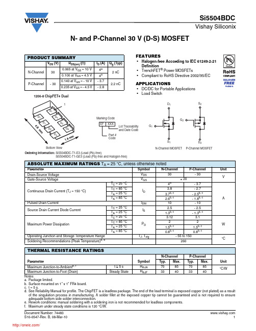
N- and P-Channel 30 V (D-S) MOSFETPRODUCT SUMMARYV DS (V)R DS(on) (Ω)I D (A)Q g (Typ)N-Channel 300.065 at V GS = 10 V 4a 2 nC 0.100 at V GS = 4.5 V 4a P-Channel- 300.140 at V GS = - 10 V - 3.7 2.2 nC0.235 at V GS = - 4.5 V- 2.8Notes:a.Package limited.b.Surface mounted on 1" x 1" FR4 board.c.t = 5 s.d.See Reliability Manual for profile. The ChipFET is a leadless package. The end of the lead terminal is exposed copper (not plated) as a result of the singulation process in manufacturing. A solder fillet at the exposed copper tip cannot be guaranteed and is not required to ensure adequade bottom side solder interconnection.e.Rework conditions: manual soldering with a soldering iron is not recommended for leadless components.f.Maximum under steady state conditions is 120 °C/W.ABSOLUTE MAXIMUM RATINGS T A = 25°C, unless otherwise notedParameter Symbol N-Channel P-Channel UnitDrain-Source VoltageV DS 30- 30VGate-Source VoltageV GS ± 20Continuous Drain Current (T J = 150 °C)T C = 25 °C I D 4a - 3.7A T C = 85 °C 3.8- 2.7T A = 25 °C 3.7b, c - 2.5b, c T A = 85 °C 2.6b, c- 1.8b, c Pulsed Drain Current I DM 10- 10Source Drain Current Diode CurrentT C = 25 °C I S 2.5- 2.5T A = 25 °C 1.3b, c - 1.3b, c Maximum Power Dissipation T C = 25 °C P D 3.12 3.1W T C = 85 °C 22T A = 25 °C 1.5b, c 1.5b, c T A = 85 °C 0.8b, c0.8b, c Operating Junction and Storage Temperature Range T J , T stg - 55 to 150°C Soldering Recommendations (Peak Temperature)d, e260THERMAL RESISTANCE RATINGSParameter Symbol N-ChannelP-ChannelUnitTyp.Max.Typ.Max.Maximum Junction-to-Ambient b, f t ≤ 5 s R thJA 70857085°C/WMaximum Junction-to-Foot (Drain)Steady State R thJF 33403340FEATURES•Halogen-free According to IEC 61249-2-21Definition•TrenchFET ® Power MOSFETs•Compliant to RoHS Directive 2002/95/ECAPPLICATIONS•DC/DC for Portable ApplicationsNotes:a. Guaranteed by design, not subject to production testing.b. Pulse test; pulse width ≤ 300 µs, duty cycle ≤ 2 %.SPECIFICATIONS T J = 25°C, unless otherwise notedParameter Symbol Test Conditions Min.Typ.Max.UnitStaticDrain-Source Breakdown Voltage V DS V GS = 0 V , I D = 250 µA N-Ch 30V V GS = 0 V, I D = - 250 µAP-Ch - 30V DS Temperature Coefficient ΔV DS /T J I D = 250 µA N-Ch 27mV/°CI D = - 250 µA P-Ch - 30V GS(th) Temperature Coefficient ΔV GS(th)/T J I D = 250 µA N-Ch - 5I D = - 250 µA P-Ch 3.5Gate Threshold Voltage V GS(th) V DS = V GS , I D = 250 µA N-Ch 1.53VV DS = V GS , I D = - 250 µA P-Ch - 1.5- 3Gate-Body LeakageI GSSV DS = 0 V , V GS = ± 20 V N-Ch 100nAP-Ch - 100Zero Gate Voltage Drain CurrentI DSSV DS = 30 V, V GS = 0 VN-Ch 1µAV DS = - 30 V , V GS = 0 V P-Ch - 1V DS = 30 V , V GS = 0 V, T J = 85 °C N-Ch 5V DS = - 30 V, V GS = 0 V , T J = 85 °CP-Ch - 5On-State Drain CurrentbI D(on)V DS ≥ 5 V , V GS = 10 V N-Ch 10A V DS ≤ - 5 V , V GS = - 10 V P-Ch - 10Drain-Source On-State Resistance b R DS(on)V GS = 10 V , I D = 3.1 A N-Ch 0.0530.065ΩV GS = - 10 V , I D = - 2.1 A P-Ch 0.1120.140V GS = 4.5 V, I D = 1 A N-Ch 0.0810.100V GS = - 4.5 V , I D = - 0.43 A P-Ch 0.1880.235Forward T ransconductance b g fsV DS = 15 V , I D = 3.1 A N-Ch 5S V DS = - 15 V , I D = - 2.1 AP-Ch 3.5Dynamic aInput Capacitance C iss N-ChannelV DS = 15 V, V GS = 0 V , f = 1 MHz P-ChannelV DS = - 15 V , V GS = 0 V , f = 1 MHz N-Ch220pFP-Ch 170Output CapacitanceC oss N-Ch 50P-Ch 50Reverse Transfer CapacitanceC rssN-Ch 25P-Ch 31Total Gate Charge Q gV DS = 15 V, V GS = 10 V, I D = 3.6 AN-Ch 4.57nC V DS = - 15 V , V GS = - 10 V , I D = - 2.5 A P-Ch 4.57N-ChannelV DS = 15 V , V GS = 4.5 V , I D = 3.6 AP-ChannelV DS = - 15 V , V GS = - 4.5 V , I D = - 2.5 AN-Ch 23P-Ch 2.2 3.5Gate-Source Charge Q gs N-Ch 0.7P-Ch 0.7Gate-Drain Charge Q gd N-Ch 0.7P-Ch 1Gate ResistanceR gf = 1 MHzN-Ch 3ΩP-Ch13Notes:a. Guaranteed by design, not subject to production testing.b. Pulse test; pulse width ≤ 300 µs, duty cycle ≤ 2 %.Stresses beyond those listed under “Absolute Maximum Ratings” may cause permanent damage to the device. These are stress ratings only, and functional operation of the device at these or any other conditions beyond those indicated in the operational sections of the specifications is not implied. Exposure to absolute maximum rating conditions for extended periods may affect device reliability.SPECIFICATIONS T J = 25°C, unless otherwise notedParameter Symbol Test Conditions Min.Typ.Max.UnitDynamic aT urn-On Delay Time t d(on) N-ChannelV DD = 15 V, R L = 5.8 Ω I D ≅ 2.6 A, V GEN = 4.5 V , R g = 1 ΩP-ChannelV DD = - 15 V , R L = 7.5 Ω I D ≅ - 2 A, V GEN = - 4.5 V , R g = 1 ΩN-Ch1525nsP-Ch 3045Rise Timet r N-Ch 80120P-Ch 6090T urn-Off Delay Time t d(off) N-Ch 1220P-Ch 1015Fall Timet f N-Ch 2540P-Ch 1015T urn-On Delay Time t d(on) N-ChannelV DD = 15 V, R L = 5.8 Ω I D ≅ 2.6 A, V GEN = 10 V , R g = 1 ΩP-ChannelV DD = - 15 V , R L = 7.5 Ω I D ≅ - 2 A, V GEN = - 10 V , R g = 1 ΩN-Ch48P-Ch 48Rise Timet r N-Ch 1220P-Ch 1015T urn-Off Delay Time t d(off) N-Ch 1015P-Ch 1015Fall Timet fN-Ch 510P-Ch510Drain-Source Body Diode Characteristics Continuous Source-Drain Diode Current I S T C = 25 °CN-Ch 2.5AP-Ch - 2.5Pulse Diode Forward Current a I SM N-Ch 10P-Ch - 10Body Diode VoltageV SD I S = 2.6 A, V GS = 0 V N-Ch 0.8 1.2V I S = - 2 A, V GS = 0 VP-Ch - 0.8- 1.2Body Diode Reverse Recovery Time t rr N-ChannelI F = 2.6 A, dI/dt = 100 A/µs, T J = 25 °C P-ChannelI F = - 2 A, dI/dt = - 100 A/µs, T J = 25 °CN-Ch 3050ns P-Ch 2040Body Diode Reverse Recovery Charge Q rr N-Ch 2040nC P-Ch 1020Reverse Recovery Fall Time t a N-Ch 23nsP-Ch 13Reverse Recovery Rise Timet bN-Ch 7P-Ch7N-CHANNEL TYPICAL CHARACTERISTICS 25°C, unless otherwise notedOutput CharacteristicsOn-Resistance vs. Drain CurrentTransfer CharacteristicsCapacitanceN-CHANNEL TYPICAL CHARACTERISTICS 25°C, unless otherwise notedSource-Drain Diode Forward VoltageThreshold VoltageSingle Pulse PowerSafe Operating Area, Junction-to-AmbientN-CHANNEL TYPICAL CHARACTERISTICS 25°C, unless otherwise noted* The power dissipation P D is based on T J(max) = 150 °C, using junction-to-case thermal resistance, and is more useful in settling the upper dissipation limit for cases where additional heatsinking is used. It is used to determine the current rating, when this rating falls below the package limit.Current Derating*Power DeratingN-CHANNEL TYPICAL CHARACTERISTICS 25°C, unless otherwise notedTransfer CharacteristicsCapacitanceOn-Resistance vs. Junction TemperatureP-CHANNEL TYPICAL CHARACTERISTICS 25°C, unless otherwise notedSource-Drain Diode Forward VoltageSingle Pulse PowerP-CHANNEL TYPICAL CHARACTERISTICS 25°C, unless otherwise noted* The power dissipation P D is based on T J(max) = 150 °C, using junction-to-case thermal resistance, and is more useful in settling the upper dissipation limit for cases where additional heatsinking is used. It is used to determine the current rating, when this rating falls below the package limit.Current Derating*分销商库存信息: VISHAYSI5504BDC-T1-E3。
Si9910DY-T1中文资料

Adaptive Power MOSFET Driver 1FEATURESD dv/dt and di/dt Control D Undervoltage Protection D Short-Circuit ProtectionD t rr Shoot-Through Current Limiting D Low Quiescent Current D CMOS Compatible InputsD Compatible with Wide Range of MOSFET Devices D Bootstrap and Charge Pump Compatible (High-Side Drive)DESCRIPTIONThe Si9910 Power MOSFET driver provides optimized gate drive signals, protection circuitry and logic level interface. Very low quiescent current is provided by a CMOS buffer and a high-current emitter-follower output stage. This efficiency allows operation in high-voltage bridge applications with “bootstrap” or “charge-pump” floating power supply techniques.The non-inverting output configuration minimizes current drain for an n-channel “on” state. The logic input is internally diode clamped to allow simple pull-down in high-side drives.Fault protection circuitry senses an undervoltage or output short-circuit condition and disables the power MOSFET.Addition of one external resistor limits maximum di/dt of the external Power MOSFET . A fast feedback circuit may be used to limit shoot-through current during t rr (diode reverse recovery time) in a bridge configuration.The Si9910 is available in 8-pin plastic DIP and SOIC packages, and are specified over the industrial, D suffix (−40to 85_C) temperature range. In SOIC-8 packaging both standard and lead (Pb)-free options are available.FUNCTIONAL BLOCK DIAGRAMV DDINPUT1.Patent Number 484116.ABSOLUTE MAXIMUM RATINGSVoltages Referenced to V SS PinV DD Supply Range −0.3 V to 18 V . . . . . . . . . . . . . . . . . . . . . . . . . . . . . . . . . . . Pin 1, 4, 5, 7, 8−0.3 V to V DD + 0.3 V . . . . . . . . . . . . . . . . . . . . . . . . . . . . . . . . Pin 2−0.7 V to V DD + 0.3 V . . . . . . . . . . . . . . . . . . . . . . . . . . . . . . . . . . . . . . . . . Input Current "20 mA . . . . . . . . . . . . . . . . . . . . . . . . . . . . . . . . . . . . . . . . . . . . . Peak Current (I pk )1 A . . . . . . . . . . . . . . . . . . . . . . . . . . . . . . . . . . . . . . . . . . . . . . Storage Temperature −65 to 150_C. . . . . . . . . . . . . . . . . . . . . . . . . . . . . . . . . . Operating Temperature −40 to 85_C . . . . . . . . . . . . . . . . . . . . . . . . . . . . . . . . . Junction Temperature (T J )150_C . . . . . . . . . . . . . . . . . . . . . . . . . . . . . . . . . . . . Power Dissipation (Package)a8-Pin SOIC (Y Suffix)b 700 mW . . . . . . . . . . . . . . . . . . . . . . . . . . . . . . . . . . . . . 8-Pin Plastic DIP (J Suffix)b 700 mW. . . . . . . . . . . . . . . . . . . . . . . . . . . . . . . . . Notesa.Device mounted with all leads soldered or welded to PC board.b.Derate 5.6 mW/_C above 25_C.SPECIFICATIONS aTest ConditionsLimitsParameterSymbolUnless Otherwise SpecifiedV DD 10.8 V to 16.5 VT A = OperatingTemperature RangeMin cTyp bMax cUnitInputHigh Level Input Voltage V IH 0.70 x V DD7.4Low Level Input Voltage V IL 6.00.35 x V DDVInput Voltage HysteresisV h0.90 2.03.0High Level Input Current I IHV IN = V DD "1Low Level Input Current IILV IN = 0 V"1m A OutputHigh Level Output Voltage V OH I OH = −200 mA V DD −310.7Low Level Output Voltage V OL I OL = 200 mA1.33Undervoltage Lockout V UVLO 8.39.210.6I SENSE Pin ThresholdV TH Max I S = 2 mA, Input High100 mV Change on Drain0.50.660.8VVoltage Drain-Source Maximum V DS Input High 8.39.110.2Input Current for V DS Input I VDS 1220.0m A Peak Output Source Current I OS+1A Peak Output Sink CurrentI OS −−1SupplySupply Range V DD 10.816.5V I DD1Output High, No Load 0.11Supply CurrentI DD2Output Low, No Load100500m ADynamicPropagation Delay Time Low to High Level t PLH 120Propagation Delay Time High to Low Level t PHL 135Rise Time t r C L = 2000 pF50nsFall Timet f 35Overcurrent Sense Delay (V DS )t DS 1m S Input CapacitanceC in5pF Notesa.Refer to PROCESS OPTION FLOWCHART for additional information.b.Typical values are for DESIGN AID ONLY , not guaranteed nor subject to production testing.c.The algebraic convention whereby the most negative value is a minimum and the most positive a maximum.AC TESTING CONDITIONSIN (IN = L)OUTV DD V SS V OH V OLPIN CONFIGURATIONS AND ORDERING INFORMATIONV DS PULL-UP INPUT PULL −DOWN V DD V SS DRAINI SENSESOIC-85678Top View2341PDIP-8V DS PULL-UP INPUT Pull-DOWN V DD V SS DRAINI SENSETop View56782341ORDERING INFORMATIONPart NumberTemperature Range PackageSi9910DY Si9910DY -T1SOIC-8Si9910DY -T1—E3−40 to 85_CSi9910DJ PDIP 8Si9910DJ-T1PDIP-8PIN DESCRIPTIONPin 1: V DSPin 1 or V DS is a sense input for the maximum source-drain voltage limit. Two microseconds after a high transition on input pin 2, an internal timer enables the V DS(max) sense circuitry. A catastrophic overcurrent condition, excessive on-resistance,or insufficient gate-drive voltage can be sensed by limiting the maximum voltage drop across the power MOSFET. An external resistor (R3) is required to protect pin 1 from overvoltage during the MOSFET “off” condition. Exceeding V DS(max) latches the Si9910 “off.” Drive is re-enabled on the next positive- going input on pin 2. If pin 1 is not used, it must be connected to pin 6 (V SS ).Pin 2: INPUTA non-inverting, Schmidt trigger input controls the state of the MOSFET gate-drive outputs and enables the protection logic.When the input is low (v V IL ), V DD is monitored for an undervoltage condition (insufficiently charged bootstrap capacitor). If an undervoltage (v V DD(min)) condition exists,the driver will ignore a turn-on input signal. An undervoltage (v V DD(min)) condition during an “on” state will not be sensed.Pin 3: V DDV DD supplies power for the driver’s internal circuitry and charging current for the power MOSFET’s gate capacitance.The Si9910 minimizes the internal I DD in the “on” state (gate-drive outputs high) allowing a “floating” power supply to be provided by charge pump or bootstrap techniques.Pin 4: DRAINDrain is an analog input to the internal dv/dt limiting circuitry.An external capacitor (C1) must be used to protect the input from exposure to the high-voltage (“off” state) drain and to set the power MOSFET’s maximum rate of dv/dt. If dv/dt feedback is not used, pin 4 must be left open.Pin 5: I SENSEI SENSE in combination with an external resistor (R 1)protects the power MOSFET from potentially catastrophic peak currents. I SENSE is an analog feedback that limits current during the power MOSFET’s transition to an “on” state. It is intended to protect power MOSFETs (in a half-bridge arrangement) from “shoot-through” current, resulting from excess di/dt and t rr of flyback diodes or from logic timing overlap. An 0.8-V drop across (R1) should indicate a current level that is approximately four times the maximum allowable load current. When the I SENSE input is not used, it should be tied to pin 6 (V SS ).Pin 6: V SSV SS is the driver’s ground return pin. The applications diagram illustrates the connection of V SS for source-referenced“floating” applications (half-bridge, high-side) and ground-referenced applications (half-bridge, low-side).Pin 7: PULL-DOWN Pin 8: PULL-UPPull-up and pull-down outputs collectively provide the power MOSFET gate with charging and discharging currents. Turn “on” or “off” di/dt can be limited by adding resistance (R 2) in series with the appropriate output.APPLICATIONS“Floating” High-Side Drive ApplicationsAs demonstrated in Figure 1, the Si9910 is intended for use as both a ground-referenced gate driver and as a “high-side”or source-referenced gate driver in half-bridge applications.Several features of the Si9910 permit its use in half-bridge high-side drive applications.A simple and inexpensive method of isolating a floating supply to power the Si9910 in high-side driver applications had to be provided. Therefore, the Si9910 was designed to be compatible with two of the most commonly used floating supply techniques: the bootstrap and the charge pump. Both of these techniques have limitations when used alone. A properly designed bootstrap circuit can provide low-impedance drive which minimizes transition losses and the charge pump circuit provides static operation.The Si9910 is configured to take advantage of either floating supply technique if the application is not sensitive to their particular limitations, or both techniques if switching losses must be minimized and static operation is necessary. The schematic above illustrates both the charge pump and bootstrap circuits used in conjunction with an Si9910 in a high-side driver application.Input signal level shifting is accomplished with a passive pull-up (R4) and n-channel MOSFET (Q2) for pull-down in applications below 500 V. T otal node capacitance defines the value of R4 needed to guarantee an input transition rate which safely exceeds the maximum dv/dt rate of the output half-bridge. Using level-shift devices with higher current capabilities may necessitate the addition of current-limiting components such as R5.Bootstrap Undervoltage LockoutWhen using a bootstrap capacitor as a high-side floating supply, care must be taken to ensure time is available to recharge the bootstrap capacitor prior to turn-on of the high-side MOSFET. As a catastrophic protection against abnormal conditions such as start-up, loss of power, etc., an internal voltage monitor has been included which monitors the bootstrap voltage when the Si9910 is in the low state. The Si9910 will not respond to a high input signal until the voltage on the bootstrap capacitor is sufficient to fully enhance the power MOSFET gate. For more details, please refer to Application Note AN705.APPLICATION CIRCUITFIGURE 1.High-Voltage Half-Bridge with Si9910 Drivers。
物理化学-第二章-热力学第一定律及其应用精选全文

上一内容 下一内容 回主目录
返回
2024/8/13
状态与状态函数
状态函数的特性: 异途同归,值变相等;周而复始,数值还原。
状态函数的性质:
(1) 状态函数的值取决于状态,状态改变则状态函数必定改 变(但不一定每个状态函数都改变);任何一个状态函数 改变,系统的状态就会改变。
上一内容 下一内容 回主目录
即
ΔU=Q+W (封闭系统)
对于无限小过程,则有
dU=δQ+δW (封闭系统)
上一内容 下一内容 回主目录
返回
2024/8/13
3. 焦耳实验 盖.吕萨克—焦尔实验
实验结果:水温未变 dT=0 dV≠0
表明:Q =0
自由膨胀 W=0
上一内容 下一内容 回主目录
返回
2024/8/13
dU= Q+ W =0
1. 热(heat)
a) 定义:体系与环境之间因温差而传递的能量称为热,用 符号Q 表示。单位:KJ 或 J。 b) Q的取号:体系吸热,Q>0;体系放热,Q<0 。
c) 性质:热不是状态函数,是一个过程量;热的大小和具 体的途径有关。
上一内容 下一内容 回主目录
返回
2024/8/13
功和热
不能说在某个状态时系统有多少热量,只能说 在某个具体过程中体系和环境交换的热是多少。
热力学能是状态函数,用符号U表示,单位为J。它 的绝对值无法测定,只能求出它的变化值。
U= U2 –U1
上一内容 下一内容 回主目录
返回
2024/8/13
热力学能
纯物质单相系统
若n确定
U=U ( n,T,V ) U=U (T,V )
电磁学--第三版--课件知识讲解

R
o
r
dr
(x2 r2)1/2
xPx
第一章 静电学的基本规律
30
电磁学
讨论
1-3 电场和电场强度
Ex( 1 1 )
2ε0 x2 x2R2
xR
E
2ε0
xR
E
4
q π ε0
x2
R
o xPx
如何求无限大均匀带电平面的电场?
第一章 静电学的基本规律
31
电磁学
1-3 电场和电场强度
E 2 0
无限大均匀带电平面的场强,匀强电场.
一般来讲,空间不同点的场强的大小和方向都是不同
的,即电场强度是 空间位置的函数, E E (x ,y ,z)
电场是矢量场,若空间各点场强的大小和方向都相同, 则称为均匀电场或匀强电场。
第一章 静电学的基本规律
2
电磁学
1-3 电场和电场强度
电场的基本特性是对场中的电荷有力的作用,若将电 量为q的点电荷置于场强为 E的某点,则该点电荷所受
1 dq
dE 4πε0
r2
er
根据场强叠加原理,整个带电体在 点P激发的场强
为
1 dq
E dE 4πε0 r2er
dq + + +
+ ++
+ e + + r
+
r
d1-3 电场和电场强度
E
1
4π0
dr2qer
计算时将上式在坐标系中进行分解,再对坐标
无限长均匀带电直线的场强
E 2 π 0a
无限长带电直导线附近某 点的场强 E大小与该点离
带电直线的距离 a成反比,
SI4401DDY-T1-GE3;中文规格书,Datasheet资料
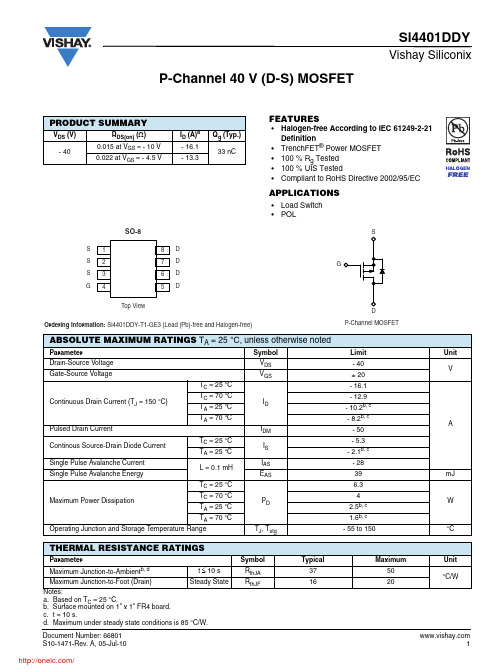
0.024 V GS = 4.5 V 0.018 V GS = 10 V 0.012
C - Capacitance (pF)
3600 Ciss 2700
1800
0.006
900
Coss Crss
0 0 10 20 30 40 50
0 0 8 16 24 32 40
ID - Drain Current (A)
0.5
1.0
1.5
2.0
VDS - Drain-to-Source Voltage (V)
VGS - Gate-to-Source Voltage (V)
Output Characteristics
0.030 4500
Transfer Characteristics
RDS(on) - On-Resistance (Ω)
50 V GS = 10 V thru 5 V 40
ID - Drain Current (A)
10
V GS = 4 V
ID - Drain Current (A)
8
30
6
20
4 T C = 25 °C 2
10 V GS = 3 V 0 0.0
T C = 125 °C 0 T C = - 55 °C 0 1 2 3 4
• Halogen-free According to IEC 61249-2-21 Definition • TrenchFET® Power MOSFET • 100 % Rg Tested • 100 % UIS Tested • Compliant to RoHS Directive 2002/95/EC
Si4401DDY
Vishay Siliconix
SIHFD9014-E3中文资料

Power MOSFETIRFD9014, SiHFD9014Vishay SiliconixFEATURES•Dynamic dV/dt Rating•Repetitive Avalanche Rated •For Automatic Insertion •End Stackable •P-Channel•175 °C Operating Temperature •Fast Switching•Lead (Pb)-free AvailableDESCRIPTIONThird generation Power MOSFETs from Vishay provide the designer with the best combination of fast switching,ruggedized device design, low on-resistance and cost-effectiveness.The 4 pin DIP package is a low cost machine-insertable case style which can be stacked in multiple combinations on standard 0.1" pin centers. The dual drain servers as a thermal link to the mounting surface for power dissipation levels up to 1 W.Notesa.Repetitive rating; pulse width limited by maximum junction temperature (see fig. 11).b.V DD = - 25 V, starting T J = 25 °C, L = 33 mH, R G = 25 Ω, I AS = - 2.2 A (see fig. 12).c.I SD ≤ - 6.7 A, dI/dt ≤ 90 A/µs, V DD ≤ V DS , T J ≤ 175 °C.d. 1.6 mm from case.PRODUCT SUMMARYV DS (V)- 60R DS(on) (Ω)V GS = - 10 V0.50Q g (Max.) (nC)12Q gs (nC) 3.8Qgd (nC) 5.1ConfigurationSingleORDERING INFORMATIONPackage HEXDIP Lead (Pb)-free IRFD9014PbF SiHFD9014-E3 SnPbIRFD9014SiHFD9014ABSOLUTE MAXIMUM RATINGS T C = 25 °C, unless otherwise notedARAMETER SYMBOL LIMIT UNIT Drain-Source Voltage V DS- 60VGate-Source Voltage V GS ± 20Continuous Drain Current V GS at - 10 VT C = 25 °C I D- 1.1A T C = 100 °C- 0.80Pulsed Drain Current a I DM - 8.8Linear Derating Factor0.0083W/°C Single Pulse Avalanche Energy b E AS 140mJ Avalanche Current aI AR - 1.1A Repetitive Avalanche Energy a E AR 0.13mJ Maximum Power Dissipation T C = 25 °CP D 1.3WPeak Diode Recovery dV/dt cdV/dt - 4.5V/ns Operating Junction and Storage Temperature Range T J , T stg- 55 to + 175°C Soldering Recommendations (Peak Temperature)for 10 s300d* Pb containing terminations are not RoHS compliant, exemptions may apply元器件交易网IRFD9014, SiHFD9014Vishay SiliconixNotesa.Repetitive rating; pulse width limited by maximum junction temperature (see fig. 11).b.Pulse width ≤ 300 µs; duty cycle ≤ 2 %.THERMAL RESISTANCE RATINGSARAMETER SYMBOL TY.MAX.UNIT Maximum Junction-to-AmbientR thJA-120°C/W 元器件交易网IRFD9014, SiHFD9014Vishay Siliconix TYPICAL CHARACTERISTICS25 °C, unless otherwise notedCCFig. 3 - Typical Transfer Characteristics元器件交易网IRFD9014, SiHFD9014 Vishay SiliconixFig. 7 - Typical Source-Drain Diode Forward VoltageFig. 8 - Maximum Safe Operating Area元器件交易网IRFD9014, SiHFD9014Vishay SiliconixFig. 9 - Maximum Drain Current vs. Case Temperature Fig. 10a - Switching Time Test CircuitFig. 10b - Switching Time WaveformsFig. 11 - Maximum Effective Transient Thermal Impedance, Junction-to-Case元器件交易网IRFD9014, SiHFD9014Vishay SiliconixFig. 12a - Unclamped Inductive Test CircuitFig. 12b - Unclamped Inductive WaveformsFig. 13a - Basic Gate Charge Waveform Fig. 13b - Gate Charge Test Circuit元器件交易网元器件交易网Vishay SiliconixVishay Siliconix maintains worldwide manufacturing capability. Products may be manufactured at one of several qualified locations. Reliability data for Silicon Technology and Package Reliability represent a composite of all qualified locations. For related documents such as package/tape drawings, part marking, and reliability data, see /ppg?91136.Disclaimer Legal Disclaimer NoticeVishayAll product specifications and data are subject to change without notice.Vishay Intertechnology, Inc., its affiliates, agents, and employees, and all persons acting on its or their behalf (collectively, “Vishay”), disclaim any and all liability for any errors, inaccuracies or incompleteness contained herein or in any other disclosure relating to any product.Vishay disclaims any and all liability arising out of the use or application of any product described herein or of any information provided herein to the maximum extent permitted by law. The product specifications do not expand or otherwise modify Vishay’s terms and conditions of purchase, including but not limited to the warranty expressed therein, which apply to these products.No license, express or implied, by estoppel or otherwise, to any intellectual property rights is granted by this document or by any conduct of Vishay.The products shown herein are not designed for use in medical, life-saving, or life-sustaining applications unless otherwise expressly indicated. Customers using or selling Vishay products not expressly indicated for use in such applications do so entirely at their own risk and agree to fully indemnify Vishay for any damages arising or resulting from such use or sale. Please contact authorized Vishay personnel to obtain written terms and conditions regarding products designed for such applications.Product names and markings noted herein may be trademarks of their respective owners.元器件交易网。
GE-CHINA材料对照表
材料对照表(2006年G版)下面是简易的材料对照表,加“*”符号的是GE公司D50A152(L)确认又经EPE批准的材料,加“**”符号的是GE-EPE“SDR”认可的材料。
在使用时设计人员应优先使用本表,本表没有的才使用NB0191。
No. GE材料中国材料 GE材料中国材料1**AISI 304L **00Cr19Ni10薄板, 棒,管,*B4A2F(S34) *20中板,角钢2 **316 **00Cr17Ni14Mo2薄板*B4A2X1(S34) *20棒, 薄板3**B4A2X1(S34)**20g中厚板**316 **0Cr17Ni12Mo2薄板,钢丝,锻件,棒4**B4A5D(S13) **20锻件**316L **00Cr17Ni14Mo2钢管,中厚板,棒5 **F316L **00Cr17Ni14Mo2钢管**B4A10(S17) **Q345A409 **00Cr19Ni10薄板,中厚板**B4A26A(S12) **20棒, 薄板6 **AISI439 **304L薄板 **B4A26A(S12)**20g中厚板7 **AISI1020 **20薄板*B4A39A(S11) *20钢管8 **AISI9 **AISI 1018-1020 **20方钢, 棒 *B4A39B(S11) *20钢管C1015 **Q235A *B4A39C(S11) *20钢管10 **AISI11 ** GR B API 5L-04 **20管 *B4A39D(S11) *20钢管12 **Gr.32510 ASTM A47-99**20钢管,棒 *B4A39E(S11) *20钢管A47-1999 **20棒**B4A45A(S9) **Q345A,H型钢,角钢,中厚板13 **ASTM14 **TYPE S CLASS A ASTM A53-04 **20钢管 **B4A47C(S5) **Q345A中厚板A105-01 **30锻件 *B4A48A(S3) *20棒15 **ASTM16 **ASTM A106 **20钢管 **B4A51B(S4) **20精制管, 管17 ** B级ASTM A106 **20钢管 **B4A56A2(S3) **16MnR厚板18 **F304L ASTM A182-05 **00Cr19Ni10锻件,钢管**B4A57B1(S2) **20精制管19 **F316 ASTM A182-05**0Cr17Ni12Mo2锻件**B5F4C(S23) **42CrMoA棒20 ** WPB ASTM A234-04 **20锻件 **B5F5B3(S26) **45CrMoV A棒21 **ASTM A276-96 TYPE316 **0Cr17Ni12Mo2棒**B7A2C(S14) **0Cr18Ni9薄板**0Cr18Ni9钢管22 **Grade B ASTM A307-04**35棒 **B7A17B(S10)23 **TP304L ASTM A312-04**00Cr19Ni10钢管**B7A17B2(S10) **0Cr18Ni9钢管24 **FP316L ASTM A312-04**00Cr17Ni14Mo2钢管**B7A25B(S5) **0Cr18Ni10Ti薄板25 **ASTM A366M-91 **SC1(**08Al) 中厚板, 薄板**B7A31A3(S10) **0Cr18Ni9棒,中厚板26 **F304L ASTM A403-04 **00Cr19Ni10锻件**B7A34C2(S16) **0Cr18Ni9薄板27 **F316L ASTM A403-04 **00Cr17Ni14Mo2锻件**B7A44C2(S4) **00Cr19Ni10钢带28 ** CS A ASTM A1008M-04 **SC1(**08Al) 中厚板,薄板**B7A54A(S4) **0Cr18Ni9中厚板,管29 **B2M1C(S31) **ZG230-450 **B7A59B(S4) **00Cr19Ni10钢管30 *B4A2(S34) *20 *B7A62A(S4) *00Cr19Ni10中厚板31 *B4A2A(S34) *20棒 *B7A63A3(S3)*00Cr19Ni10中厚板,棒,管32 *B4A2A(S34)*Q235A薄板 *B7A68B(S9) *00Cr19Ni10薄板,中厚板33 **B4A2A(S34)**20g中厚板 **B7A68C2(S9) **00Cr19Ni10薄板34 *B4A2C(S34) *20 **B7A80A2(S4) **00Cr17Ni14Mo2薄板35 **B4A2C4(S34) **20g中厚板 *B7A82A3(S5) *0Cr17Ni12Mo2棒材料对照表(2006年G版)下面是简易的材料对照表,加“*”符号的是GE公司D50A152(L)确认又经EPE批准的材料,加“**”符号的是GE-EPE“SDR”认可的材料。
高档DV电路
41
D
DGND
DGND
PVDD
AVDD1
VCOML
VCOMH
PCDL
DGND
DGND
DGND
DGND
DGND
FPC 0.5mm Pitch 40pin Top Contact ZIF
C157 1uF/16V 0603C
C158 1uF/16V 0603C
C159 2.2uF/16V 0603C
C160 2.2uF/16V 0603C
LED_POWER A2_GPIO43 E
B Q6 MMBT3904 R135 24R C1,1F.,NO1,Li-Hsin 1st. Rd.,Hsinchu Science Park,Hsinchu City 30078,Taiwan, R.O.C. TEL:+886-3-666-8828 FAX:+886-3-666-1282
2 1
AV33_AUD
C
AUDIO-OUT MICMIC1 MIC MIC+
VCOM
VCOC
AVDD
AVSS
PDN
1K
CSN
1
2
3
4
5
6
C126
1uF C168 10uF
ASGND R108 DGND
SVSS SVDD AOUT BEEP/MICN MPI MIC/MICP U8 AKM4633
BICK FCK SDTO SDTI CDTI CCLK
0.1uF 0.1uF 0.1uF 0.1uF 0.1uF 0.1uF 0.1uF 0.1uF 0.1uF 0.1uF 0.1uF 0.1uF 0.1uF 0.1uF 0.1uF
SI9910DY-E3;SI9910DJ-E3;中文规格书,Datasheet资料

Si9910 Vishay SiliconixDocument Number: 70009 S-42043—Rev. H, 15-Nov-041 Adaptive Power MOSFET Driver1FEATURESD dv/dt and di/dt Control D Undervoltage Protection D Short-Circuit Protection D t rr Shoot-Through Current LimitingD Low Quiescent CurrentD CMOS Compatible InputsD Compatible with Wide Range of MOSFET DevicesD Bootstrap and Charge Pump Compatible(High-Side Drive)DESCRIPTIONThe Si9910 Power MOSFET driver provides optimized gate drive signals, protection circuitry and logic level interface. Very low quiescent current is provided by a CMOS buffer and a high-current emitter-follower output stage. This efficiency allows operation in high-voltage bridge applications with “bootstrap” or “charge-pump” floating power supply techniques.The non-inverting output configuration minimizes current drain for an n-channel “on” state. The logic input is internally diode clamped to allow simple pull-down in high-side drives.Fault protection circuitry senses an undervoltage or output short-circuit condition and disables the power MOSFET. Addition of one external resistor limits maximum di/dt of the external Power MOSFET. A fast feedback circuit may be used to limit shoot-through current during t rr (diode reverse recovery time) in a bridge configuration.The Si9910 is available in both standard and lead (Pb)-free 8-pin plastic DIP and SOIC packages which are specified to operate over the industrial temperature range of −40_C to 85_C.FUNCTIONAL BLOCK DIAGRAMV DDINPUT1.Patent Number 484116.Si9910Vishay Siliconix2Document Number: 70009S-42043—Rev. H, 15-Nov-04ABSOLUTE MAXIMUM RATINGSVoltages Referenced to V SS PinV DD Supply Range −0.3 V to 18 V . . . . . . . . . . . . . . . . . . . . . . . . . . . . . . . . . . . Pin 1, 4, 5, 7, 8−0.3 V to V DD + 0.3 V . . . . . . . . . . . . . . . . . . . . . . . . . . . . . . . . Pin 2−0.7 V to V DD + 0.3 V . . . . . . . . . . . . . . . . . . . . . . . . . . . . . . . . . . . . . . . . . Input Current "20 mA . . . . . . . . . . . . . . . . . . . . . . . . . . . . . . . . . . . . . . . . . . . . . Peak Current (I pk )1 A . . . . . . . . . . . . . . . . . . . . . . . . . . . . . . . . . . . . . . . . . . . . . . Storage Temperature −65 to 150_C. . . . . . . . . . . . . . . . . . . . . . . . . . . . . . . . . . Operating Temperature −40 to 85_C . . . . . . . . . . . . . . . . . . . . . . . . . . . . . . . . . Junction Temperature (T J )150_C . . . . . . . . . . . . . . . . . . . . . . . . . . . . . . . . . . . . Power Dissipation (Package)a8-Pin SOIC (Y Suffix)b 700 mW . . . . . . . . . . . . . . . . . . . . . . . . . . . . . . . . . . . . . 8-Pin Plastic DIP (J Suffix)b 700 mW. . . . . . . . . . . . . . . . . . . . . . . . . . . . . . . . . Notesa.Device mounted with all leads soldered or welded to PC board.b.Derate 5.6 mW/_C above 25_C.Stresses beyond those listed under “Absolute Maximum Ratings” may cause permanent damage to the device. These are stress ratings only, and functional operation of the device at these or any other conditions beyond those indicated in the operational sections of the specifications is not implied. Exposure to absolute maximum rating conditions for extended periods may affect device reliability.SPECIFICATIONS aTest ConditionsLimitsParameterSymbolUnless Otherwise SpecifiedV DD 10.8 V to 16.5 VT A = OperatingTemperature RangeMin cTyp bMax cUnitInputHigh Level Input Voltage V IH 0.70 x V DD7.4Low Level Input Voltage V IL 6.00.35 x V DDVInput Voltage Hysteresis V h 0.90 2.03.0High Level Input Current I IH V IN = V DD "1Low Level Input CurrentI ILV IN = 0 V"1m A OutputHigh Level Output Voltage V OH I OH = −200 mA V DD −310.7Low Level Output Voltage V OL I OL = 200 mA1.33Undervoltage Lockout V UVLO 8.39.210.6I SENSE Pin ThresholdV TH Max I S = 2 mA, Input High 100 mV Change on Drain0.50.660.8VVoltage Drain-Source Maximum V DS Input High 8.39.110.2Input Current for V DS Input I VDS 1220.0m A Peak Output Source Current I OS+1A Peak Output Sink CurrentI OS −−1SupplySupply Range V DD 10.816.5V I DD1Output High, No Load 0.11Supply CurrentI DD2Output Low, No Load100500m ADynamicPropagation Delay Time Low to High Level t PLH 120Propagation Delay Time High to Low Level t PHL 135Rise Time t r C L = 2000 pF50nsFall Timet f 35Overcurrent Sense Delay (V DS )t DS 1m S Input CapacitanceC in5pF Notesa.Refer to PROCESS OPTION FLOWCHART for additional information.b.Typical values are for DESIGN AID ONLY , not guaranteed nor subject to production testing.c.The algebraic convention whereby the most negative value is a minimum and the most positive a maximum.Si9910Vishay SiliconixDocument Number: 70009S-42043—Rev. H, 15-Nov-043AC TESTING CONDITIONSIN (IN = L)OUTV DD V SS V OH V OLPIN CONFIGURATIONS AND ORDERING INFORMATIONV DS PULL-UP INPUT PULL −DOWN V DD V SS DRAINI SENSESOIC-85678Top View2341PDIP-8V DS PULL-UP INPUT Pull-DOWN V DD V SS DRAINI SENSETop View56782341ORDERING INFORMATIONPart NumberTemperature Range PackageSi9910DY Si9910DY -T1SOIC-8Si9910DY -T1—E3−40 to 85_CSi9910DJ PDIP 8Si9910DJ—E3PDIP-8Si9910Vishay Siliconix 4Document Number: 70009 S-42043—Rev. H, 15-Nov-04PIN DESCRIPTIONPin 1: V DSPin 1 or V DS is a sense input for the maximum source-drain voltage limit. Two microseconds after a high transition on input pin 2, an internal timer enables the V DS(max)sense circuitry. A catastrophic overcurrent condition, excessive on-resistance, or insufficient gate-drive voltage can be sensed by limiting the maximum voltage drop across the power MOSFET. An external resistor (R3) is required to protect pin 1 from overvoltage during the MOSFET “off” condition. Exceeding V DS(max) latches the Si9910 “off.” Drive is re-enabled on the next positive- going input on pin 2. If pin 1 is not used, it must be connected to pin 6 (V SS).Pin 2: INPUTA non-inverting, Schmidt trigger input controls the state of the MOSFET gate-drive outputs and enables the protection logic. When the input is low (v V IL), V DD is monitored for an undervoltage condition (insufficiently charged bootstrap capacitor). If an undervoltage (v V DD(min)) condition exists, the driver will ignore a turn-on input signal. An undervoltage (v V DD(min)) condition during an “on” state will not be sensed.Pin 3: V DDV DD supplies power for the driver’s internal circuitry and charging current for the power MOSFET’s gate capacitance. The Si9910 minimizes the internal I DD in the “on” state (gate-drive outputs high) allowing a “floating” power supply to be provided by charge pump or bootstrap techniques.Pin 4: DRAINDrain is an analog input to the internal dv/dt limiting circuitry. An external capacitor (C1) must be used to protect the input from exposure to the high-voltage (“off” state) drain and to set the power MOSFET’s maximum rate of dv/dt. If dv/dt feedback is not used, pin 4 must be left open.Pin 5: I SENSEI SENSE in combination with an external resistor (R1) protects the power MOSFET from potentially catastrophic peak currents. I SENSE is an analog feedback that limits current during the power MOSFET’s transition to an “on” state. It is intended to protect power MOSFETs (in a half-bridge arrangement) from “shoot-through” current, resulting from excess di/dt and t rr of flyback diodes or from logic timing overlap. An 0.8-V drop across (R1) should indicate a current level that is approximately four times the maximum allowable load current. When the I SENSE input is not used, it should be tied to pin 6 (V SS).Pin 6: V SSV SS is the driver’s ground return pin. The applications diagram illustrates the connection of V SS for source-referenced “floating” applications (half-bridge, high-side) and ground-referenced applications (half-bridge, low-side).Pin 7: PULL-DOWNPin 8: PULL-UPPull-up and pull-down outputs collectively provide the power MOSFET gate with charging and discharging currents. Turn “on” or “off” di/dt can be limited by adding resistance (R2) in series with the appropriate output.APPLICATIONS“Floating” High-Side Drive ApplicationsAs demonstrated in Figure 1, the Si9910 is intended for use as both a ground-referenced gate driver and as a “high-side”or source-referenced gate driver in half-bridge applications. Several features of the Si9910 permit its use in half-bridge high-side drive applications.A simple and inexpensive method of isolating a floating supply to power the Si9910 in high-side driver applications had to be provided. Therefore, the Si9910 was designed to be compatible with two of the most commonly used floating supply techniques: the bootstrap and the charge pump. Both of these techniques have limitations when used alone. A properly designed bootstrap circuit can provide low-impedance drive which minimizes transition losses and the charge pump circuit provides static operation.The Si9910 is configured to take advantage of either floating supply technique if the application is not sensitive to their particular limitations, or both techniques if switching losses must be minimized and static operation is necessary. The schematic above illustrates both the charge pump and bootstrap circuits used in conjunction with an Si9910 in a high-side driver application.Input signal level shifting is accomplished with a passive pull-up (R4) and n-channel MOSFET (Q2) for pull-down in applications below 500 V. T otal node capacitance defines the value of R4 needed to guarantee an input transition rate which safely exceeds the maximum dv/dt rate of the output half-bridge. Using level-shift devices with higher current capabilities may necessitate the addition of current-limiting components such as R5.Bootstrap Undervoltage LockoutWhen using a bootstrap capacitor as a high-side floating supply, care must be taken to ensure time is available to recharge the bootstrap capacitor prior to turn-on of the high-side MOSFET. As a catastrophic protection against abnormal conditions such as start-up, loss of power, etc., an internal voltage monitor has been included which monitors the bootstrap voltage when the Si9910 is in the low state. The Si9910 will not respond to a high input signal until the voltage on the bootstrap capacitor is sufficient to fully enhance the power MOSFET gate. For more details, please refer to Application Note AN705.Si9910 Vishay SiliconixDocument Number: 70009 S-42043—Rev. H, 5APPLICATION CIRCUITV (12 to 15 V)VFIGURE 1.High-Voltage Half-Bridge with Si9910 DriversVishay Siliconix maintains worldwide manufacturing capability. Products may be manufactured at one of several qualified locations. Reliability data for Silicon T echnology and Package Reliability represent a composite of all qualified locations. For related documents such as package/tape drawings, part marking, and reliability data, see /ppg?70009.Legal Disclaimer NoticeVishayDisclaimerAll product specifications and data are subject to change without notice.Vishay Intertechnology, Inc., its affiliates, agents, and employees, and all persons acting on its or their behalf (collectively, “Vishay”), disclaim any and all liability for any errors, inaccuracies or incompleteness contained herein or in any other disclosure relating to any product.Vishay disclaims any and all liability arising out of the use or application of any product described herein or of any information provided herein to the maximum extent permitted by law. The product specifications do not expand or otherwise modify Vishay’s terms and conditions of purchase, including but not limited to the warranty expressed therein, which apply to these products.No license, express or implied, by estoppel or otherwise, to any intellectual property rights is granted by this document or by any conduct of Vishay.The products shown herein are not designed for use in medical, life-saving, or life-sustaining applications unless otherwise expressly indicated. Customers using or selling Vishay products not expressly indicated for use in such applications do so entirely at their own risk and agree to fully indemnify Vishay for any damages arising or resulting from such use or sale. Please contact authorized Vishay personnel to obtain written terms and conditions regarding products designed for such applications.Product names and markings noted herein may be trademarks of their respective owners.Document Number: Revision: 18-Jul-081分销商库存信息:VISHAYSI9910DY-E3SI9910DJ-E3。
SIHLZ44-E3中文资料

Power MOSFETIRLZ44, SiHLZ44Vishay SiliconixFEATURES•Dynamic dV/dt Rating •Logic-Level Gate Drive•R DS(on) Specified at V GS = 4 V and 5 V •175 °C Operating Temperature •Fast Switching •Ease of Paralleling •Simple Drive Requirements •Lead (Pb)-free AvailableDESCRIPTIONThird generation Power MOSFETs from Vishay provide the designer with the best combination of fast switching,ruggedized device design, low on-resistance and cost-effectiveness.The TO-220 package is universally preferred for all commercial-industrial applications at power dissipation levels to approximately 50 W. The low thermal resistance and low package cost of the TO-220 contribute to its wide acceptance throughout the industry.Notesa.Repetitive rating; pulse width limited by maximum junction temperature (see fig. 11).b.V DD = 25 V, starting T J = 25 °C, L = 179 µH, R G = 25 Ω I AS = 51 A (see fig. 12).c.I SD ≤ 51 A, dV/dt ≤ 250 A/s, V DD ≤ V DS , T J ≤ 175 °C.d. 1.6 mm from case.e.Current limited by the package, (die current = 51 A).PRODUCT SUMMARYV DS (V)60 VR DS(on) (Ω)V GS = 5.0 V0.028Q g (Max.) (nC)66Q gs (nC)12Q gd (nC)43ConfigurationSingleTO-220GDSORDERING INFORMATIONPackage TO-220Lead (Pb)-free IRLZ44PbF SiHLZ44-E3SnPbIRLZ44SiHLZ44ABSOLUTE MAXIMUM RATINGS T C = 25 °C, unless otherwise notedARAMETER SYMBOL LIMIT UNITGate-Source Voltage V GS ± 10VContinuous Drain Current e V GS at 5.0 VT C = 25 °C I D50A Continuous Drain Current T C = 100 °C36Pulsed Drain Current a I DM 200Linear Derating Factor1.0W/°C Single Pulse Avalanche Energy b E AS 400mJ Maximum Power Dissipation T C = 25 °CP D 150WPeak Diode Recovery dV/dt cdV/dt 4.5V/ns Operating Junction and Storage Temperature Range T J , T stg- 55 to + 175°C Soldering Recommendations (Peak Temperature)d for 10 s 300Mounting Torque6-32 or M3 screw10 lbf · in 1.1N · m * Pb containing terminations are not RoHS compliant, exemptions may applyIRLZ44, SiHLZ44Vishay SiliconixNotesa.Repetitive rating; pulse width limited by maximum junction temperature (see fig. 11).b.Pulse width ≤ 300 µs; duty cycle ≤ 2 %.c.Current limited by the package, (die current = 51 A).THERMAL RESISTANCE RATINGSARAMETER SYMBOL TY.MAX.UNITMaximum Junction-to-Ambient R thJA -62°C/W Case-to-Sink, Flat, Greased Surface R thCS 0.50-Maximum Junction-to-Case (Drain)R thJC- 1.0IRLZ44, SiHLZ44Vishay Siliconix TYPICAL CHARACTERISTICS 25 °C, unless otherwise notedFig. 1 - Typical Output Characteristics, T C = 25 °C Fig. 2 - Typical Output Characteristics, T C = 175 °C Fig. 3 - Typical Transfer CharacteristicsFig. 4 - Normalized On-Resistance vs. TemperatureIRLZ44, SiHLZ44 Vishay SiliconixFig. 5 - Typical Capacitance vs. Drain-to-Source Voltage Fig. 6 - Typical Gate Charge vs. Gate-to-Source Voltage Fig. 7 - Typical Source-Drain Diode Forward VoltageFig. 8 - Maximum Safe Operating AreaIRLZ44, SiHLZ44Vishay SiliconixFig. 9 - Maximum Drain Current vs. Case Temperature Fig. 10a - Switching Time Test CircuitFig. 10b - Switching Time WaveformsFig. 11 - Maximum Effective Transient Thermal Impedance, Junction-to-CaseFig. 12a - Unclamped Inductive Test CircuitFig. 12b - Unclamped Inductive WaveformsIRLZ44, SiHLZ44Vishay SiliconixFig. 12c - Maximum Avalanche Energy vs. Drain CurrentFig. 13a - Basic Gate Charge WaveformFig. 13b - Gate Charge Test CircuitIRLZ44, SiHLZ44Vishay Siliconix Array Fig. 14 - For N-ChannelVishay Siliconix maintains worldwide manufacturing capability. Products may be manufactured at one of several qualified locations. Reliability data for Silicon Technology and Package Reliability represent a composite of all qualified locations. For related documents such as package/tape drawings, part marking, andreliability data, see /ppg?91328.Disclaimer Legal Disclaimer NoticeVishayAll product specifications and data are subject to change without notice.Vishay Intertechnology, Inc., its affiliates, agents, and employees, and all persons acting on its or their behalf (collectively, “Vishay”), disclaim any and all liability for any errors, inaccuracies or incompleteness contained herein or in any other disclosure relating to any product.Vishay disclaims any and all liability arising out of the use or application of any product described herein or of any information provided herein to the maximum extent permitted by law. The product specifications do not expand or otherwise modify Vishay’s terms and conditions of purchase, including but not limited to the warranty expressed therein, which apply to these products.No license, express or implied, by estoppel or otherwise, to any intellectual property rights is granted by this document or by any conduct of Vishay.The products shown herein are not designed for use in medical, life-saving, or life-sustaining applications unless otherwise expressly indicated. Customers using or selling Vishay products not expressly indicated for use in such applications do so entirely at their own risk and agree to fully indemnify Vishay for any damages arising or resulting from such use or sale. Please contact authorized Vishay personnel to obtain written terms and conditions regarding products designed for such applications.Product names and markings noted herein may be trademarks of their respective owners.元器件交易网。
SI2333CDS-T1-E3中文资料

Vishay SiliconixSi2333CDSP-Channel 12-V (D-S) MOSFETFEATURES•TrenchFET ® Power MOSFET APPLICATIONS•Load Switch •PA SwitchMOSFET PRODUCT SUMMARYV DS (V)R DS(on) (Ω)ID (A)a Q g (Typ.)- 120.035 at V GS = - 4.5 V- 5.19 nC 0.045 at V GS = - 2.5 V - 4.50.059 at V GS = - 1.8 V- 3.9Notes:a. Based on T C = 25 °C.b. Surface Mounted on 1" x 1" FR4 board.c. t = 5 s.d. Maximum under Steady State conditions is 166 °C/W.ABSOLUTE MAXIMUM RATINGS T A = 25°C, unless otherwise notedParameter Symbol Limit UnitDrain-Source Voltage V DS - 12VGate-Source Voltage V GS± 8Continuous Drain Current (T J = 150 °C)T C = 25 °C I D- 7.1A T C = 70 °C - 5.7T A = 25 °C - 5.1b, c T A = 70 °C - 4.0b, cPulsed Drain Current I DM - 20Continuous Source-Drain Diode CurrentT C = 25 °C I S - 1.0T A = 25 °C - 0.63b, c Maximum Power Dissipation T C = 25 °C P D 2.5WT C = 70 °C 1.6T A = 25 °C 1.25b, c T A = 70 °C 0.8b, cOperating Junction and Storage T emperature Range T J , T stg - 55 to 150°C THERMAL RESISTANCE RATINGSParameter Symbol Typical Maximum UnitMaximum Junction-to-Ambient b, d≤ 5 s R thJA 75100°C/WMaximum Junction-to-Foot (Drain)Steady State R thJF 4050Vishay SiliconixSi2333CDSNotes:a. Pulse test; pulse width ≤ 300 µs, duty cycle ≤ 2 %.b. Guaranteed by design, not subject to production testing.Stresses beyond those listed under “Absolute Maximum Ratings” may cause permanent damage to the device. These are stress ratings only, and functional operation of the device at these or any other conditions beyond those indicated in the operational sections of the specifications is not implied. Exposure to absolute maximum rating conditions for extended periods may affect device reliability.MOSFET SPECIFICATIONS T J = 25°C, unless otherwise notedParameter Symbol Test Conditions Min.Typ.Max.UnitStaticDrain-Source Breakdown Voltage V DS V DS = 0 V, I D = - 250 µA- 12V V DS Temperature Coefficient ΔV DS /T J I D = - 250 µA - 13mV/°C V GS(th) T emperature Coefficient ΔV GS(th)/T J 2.6Gate-Source Threshold Voltage V GS(th) V DS = V GS , I D = - 250 µA - 0.4- 1V Gate-Source LeakageI GSS V DS = 0 V , V GS = ± 8 V ± 100nA Zero Gate Voltage Drain Current I DSS V DS = - 12 V , V GS = 0 V - 1µA V DS = - 12 V, V GS = 0 V , T J = 55 °C- 10On-State Drain Current aI D(on) V DS ≤ - 5 V , V GS = - 4.5 V - 20ADrain-Source On-State Resistance a R DS(on) V GS = - 4.5 V, I D = - 5.1 A 0.02850.035ΩV GS = - 2.5 V, I D = - 4.5 A 0.0360.045V GS = - 1.8 V, I D = - 2.0 A 0.0460.059Forward T ransconductance a g fsV DS = - 5 V , I D = - 1.9 A1.6S Dynamic bInput Capacitance C iss V DS = - 6 V , V GS = 0 V , f = 1 MHz1225pFOutput CapacitanceC oss 315Reverse Transfer Capacitance C rss 260Total Gate Charge Q g V DS = - 6 V , V GS = - 4.5 V, ID = - 5.1 A 1525nC V DS = - 6 V , V GS = - 2.5 V, I D = - 5.1 A 915Gate-Source Charge Q gs 1.9Gate-Drain Charge Q gd 3.8Gate Resistance R g f = 1 MHz4.0ΩTurn-On Delay Time t d(on) V DD = - 6 V, R L = 6 ΩI D = - 1 A, V GEN = - 4.5 V , R G = 1 Ω1320ns Rise Timet r 3560Turn-Off Delay Time t d(off) 4570Fall Timet f1220Drain-Source Body Diode Characteristics Continuous Source-Drain Diode Current I S T C = 25 °C- 1.0A Pulse Diode Forward Current a I SM - 20Body Diode VoltageV SD I S = - 1.0 A- 0.7- 1.2V Body Diode Reverse Recovery Time t rr I F = - 1.0 A, dI/dt = 100 A/µs, T J = 25 °C3250ns Body Diode Reverse Recovery Charge Q rr 2040nC Reverse Recovery Fall Time t a 16nsReverse Recovery Rise Timet b16On-Resistance vs. Drain Current and Gate VoltageCapacitanceOn-Resistance vs. Junction TemperatureThreshold VoltageVishay SiliconixSi2333CDSTYPICAL CHARACTERISTICS 25°C, unless otherwise notedVishay Siliconix maintains worldwide manufacturing capability. Products may be manufactured at one of several qualified locations. Reliability data for Silicon Technology and Package Reliability represent a composite of all qualified locations. For related documents such as package/tape drawings, part marking, and reliability data, see /ppg?68717.Normalized Thermal Transient Impedance, Junction-to-FootDisclaimer Legal Disclaimer NoticeVishayAll product specifications and data are subject to change without notice.Vishay Intertechnology, Inc., its affiliates, agents, and employees, and all persons acting on its or their behalf (collectively, “Vishay”), disclaim any and all liability for any errors, inaccuracies or incompleteness contained herein or in any other disclosure relating to any product.Vishay disclaims any and all liability arising out of the use or application of any product described herein or of any information provided herein to the maximum extent permitted by law. The product specifications do not expand or otherwise modify Vishay’s terms and conditions of purchase, including but not limited to the warranty expressed therein, which apply to these products.No license, express or implied, by estoppel or otherwise, to any intellectual property rights is granted by this document or by any conduct of Vishay.The products shown herein are not designed for use in medical, life-saving, or life-sustaining applications unless otherwise expressly indicated. Customers using or selling Vishay products not expressly indicated for use in such applications do so entirely at their own risk and agree to fully indemnify Vishay for any damages arising or resulting from such use or sale. Please contact authorized Vishay personnel to obtain written terms and conditions regarding products designed for such applications.Product names and markings noted herein may be trademarks of their respective owners.元器件交易网。
- 1、下载文档前请自行甄别文档内容的完整性,平台不提供额外的编辑、内容补充、找答案等附加服务。
- 2、"仅部分预览"的文档,不可在线预览部分如存在完整性等问题,可反馈申请退款(可完整预览的文档不适用该条件!)。
- 3、如文档侵犯您的权益,请联系客服反馈,我们会尽快为您处理(人工客服工作时间:9:00-18:30)。
Vishay SiliconixSi3438DVN-Channel 40-V (D-S) MOSFETFEATURES•T renchFET ® Power MOSFETAPPLICATIONS•DC/DC ConverterPRODUCT SUMMARYV DS (V)R DS(on) (Ω)I D (A)aQ g (Typ.)400.0355 at V GS = 10 V 7.4 5.3 nC0.0425 at V GS = 4.5 V6.7Notes:a.Based on 25 °C.b.Surface mounted on 1" x 1" FR4 board.c.t = 5 s.d.Maximum under Steady State conditions is 110 °C/W.ABSOLUTE MAXIMUM RATINGS T A = 25 °C, unless otherwise notedParameter Symbol Limit UnitDrain-Source Voltage V DS 40VGate-Source VoltageV GS ± 20Continuous Drain Current (T J = 150 °C)T C = 25 °C I D7.4A T C = 70 °C 5.8T A = 25 °C 5.5b, c T A = 70 °C 4.4b, cPulsed Drain CurrentI DM 20Continuous Source-Drain Diode CurrentT C = 25 °CI S 2.9T A = 25 °C 1.6b,cMaximum Power DissipationT C = 25 °CP D 3.5W T C = 70 °C 2.2T A = 25 °C 2b,c T A = 70 °C 1.25b,cOperating Junction and Storage T emperature Range T J , T stg - 55 to 150°CTHERMAL RESISTANCE RATINGSParameter Symbol Typical Maximum UnitMaximum Junction-to-Ambientb, d t ≤ 5 s R thJA 5062.5°C/WMaximum Junction-to-Foot Steady State R thJF 2835Vishay SiliconixSi3438DVNotes:a. Pulse test; pulse width ≤ 300 µs, duty cycle ≤ 2 %.b. Guaranteed by design, not subject to production testing.Stresses beyond those listed under “Absolute Maximum Ratings” may cause permanent damage to the device. These are stress ratings only, and functional operation of the device at these or any other conditions beyond those indicated in the operational sections of the specifications is not implied. Exposure to absolute maximum rating conditions for extended periods may affect device reliability.SPECIFICATIONS T J = 25 °C, unless otherwise notedParameter Symbol T est Condition Min.T yp.Max.UnitStaticDrain-Source Breakdown Voltage V DS V GS = 0 V , I D = 250 µA40V V DS Temperature Coefficient ΔV DS /T J I D = 250 µA 44mV/°C V GS(th) T emperature Coefficient ΔV GS(th)/T J - 5.5Gate-Source Threshold Voltage V GS(th) V DS = V GS , I D = 250 µA 1.43V Gate-Source LeakageI GSS V DS = 0 V, V GS = ± 20 V ± 100nA Zero Gate Voltage Drain Current I DSS V DS = 40 V , V GS = 0 V 1µA V DS = 40 V , V GS = 0 V , T J = 55 °C10On-State Drain Current aI D(on) V DS ≥ 5 V , V GS = 10 V 10A Drain-Source On-State Resistance a R DS(on) V GS = 10 V, I D = 5 A 0.02950.0355ΩV GS = 4.5 V , I D = 4 A 0.03550.0425Forward T ransconductance a g fs V DS = 10 V, I D = 5 A22SDynamic bInput Capacitance C iss V DS = 20 V , V GS = 0 V , f = 1 MHz640pFOutput CapacitanceC oss 73Reverse Transfer Capacitance C rss 41Total Gate Charge Q g V DS = 20 V , V GS = 10 V , ID = 5 A 11.720nC V DS = 20 V , V GS = 4.5 V , I D = 5 A 5.39Gate-Source Charge Q gs 1.9Gate-Drain Charge Q gd 1.7Gate Resistance R g f = 1 MHz0.452.2 4.4ΩTurn-On Delay Time t d(on) V DD = 20 V , R L = 4 Ω I D ≅ 5 A, V GEN = 4.5 V , R g = 1 Ω1630ns Rise Timet r 1735Turn-Off DelayTime t d(off) 1630Fall Timet f1020Turn-On Delay Time t d(on) V DD = 20 V , R L = 4 Ω I D ≅ 5 A, V GEN = 10 V , R g = 1 Ω714Rise Timet r 1020Turn-Off DelayTime t d(off) 1530Fall Timet f 918Drain-Source Body Diode Characteristics Continous Source-Drain Diode Current I S T C = 25 °C2.9A Pulse Diode Forward Current I SM 20Body Diode VoltageV SD I S = 1.7 A, V GS = 0 V0.78 1.2V Body Diode Reverse Recovery Time t rr I F = 3 A, dI/dt = 100 A/µs, T J = 25 °C1935ns Body Diode Reverse Recovery Charge Q rr 1430nC Reverse Recovery Fall Time t a 13nsReverse Recovery Rise Timet b6On-Resistance vs. Drain Current and Gate VoltageGate ChargeTransfer CharacteristicsOn-Resistance vs. Junction TemperatureThreshold VoltageOn-Resistance vs. Gate-to-Source TemperatureSingle Pulse Power, Junction-to-AmbientSafe Operating Area, Junction-to-AmbientVishay SiliconixSi3438DVTYPICAL CHARACTERISTICS 25 °C, unless otherwise noted* The power dissipation P D is based on T J(max) = 150 °C, using junction-to-case thermal resistance, and is more useful in settling the upper dissipation limit for cases where additional heatsinking is used. It is used to determine the current rating, when this rating falls below the package limit.Current Derating*Vishay SiliconixSi3438DVTYPICAL CHARACTERISTICS 25 °C, unless otherwise notedVishay Siliconix maintains worldwide manufacturing capability. Products may be manufactured at one of several qualified locations. Reliability data for Silicon Technology and Package Reliability represent a composite of all qualified locations. For related documents such as package/tape drawings, part marking, and reliability data, see /ppg?68393.Disclaimer Legal Disclaimer NoticeVishayAll product specifications and data are subject to change without notice.Vishay Intertechnology, Inc., its affiliates, agents, and employees, and all persons acting on its or their behalf (collectively, “Vishay”), disclaim any and all liability for any errors, inaccuracies or incompleteness contained herein or in any other disclosure relating to any product.Vishay disclaims any and all liability arising out of the use or application of any product described herein or of any information provided herein to the maximum extent permitted by law. The product specifications do not expand or otherwise modify Vishay’s terms and conditions of purchase, including but not limited to the warranty expressed therein, which apply to these products.No license, express or implied, by estoppel or otherwise, to any intellectual property rights is granted by this document or by any conduct of Vishay.The products shown herein are not designed for use in medical, life-saving, or life-sustaining applications unless otherwise expressly indicated. Customers using or selling Vishay products not expressly indicated for use in such applications do so entirely at their own risk and agree to fully indemnify Vishay for any damages arising or resulting from such use or sale. Please contact authorized Vishay personnel to obtain written terms and conditions regarding products designed for such applications.Product names and markings noted herein may be trademarks of their respective owners.元器件交易网。