VIPER22 BUCK BUCK
VIPER22A学习资料及原理图要点总结计划

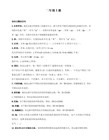
VIPER-22A资料及原理图(六祖故土人编) VIPER-22A中文资料:1(六祖故土人编)HR500-2型全能表R×1kΩ档估测的内阻值:黑表笔(脚)红表笔(脚)电阻(Ω)1、22、101、231、241、25、6、7、831、23435、6、7、841、211k4345、6、7、85k5、6、7、81、2120k5、6、7、83125k5、6、7、84140k234(六祖故土人编)VIPER22A芯片概括:意法半导体的VIPER22A芯片为专用开关电源集成电路。
其内部构造如图1所示。
芯片工作时,直流电压从漏极脚进入集成电路,经整流和稳压后供应开关电源工作,进而使这个电路工作时不需要外接启动电阻。
即便VDD供电电路不正常,电源电路的振荡电路还能起振,并且上图1VIPER22A芯片内部构造电路有输出电压。
在VDD正常前,由芯片内部自己供电,经过很短时间后,VDD供电电源正常,此时,利用门电路控制开关电路(ON/OFF)断开从栅极输入的供电回路。
VIPER22A有过热、过压保护功能。
VDD从4脚输入后,第一送入比较器,一旦输入VDD≥42V,则触发器(FF1)输出一个置位信号1使控制振荡电路工作的触发器(FF2)输出为0,锁住U2,振荡信号没法输出,即开关管不工作。
当输入电压小于1415V时,U3也将输出一个复位脉冲,使开关管不工作。
当电经过热时,R1为1,将FF2置0,开关管不工作。
当供电电压VDD在正常范围时,FB所得的取样电压与基准电压0123V对比较,用其比较结果去控制FF2的变换频次,进而控制开关管的状态变换,实现控制输出电压,达稳压的功能。
该集成电路芯片内部包括60kHz的振荡电路,其外头电路相当简单。
3VIPER22A开关电源电路本文所使用的VIPER22A芯片拥有优秀的控制功能,使得外头电路的设计较简单,只要考虑一般的短路、过载电路保护即可。
电路原理图如图2。
图2电路原理图(下列图)在沟通电源的输入端接电容C0用于滤除低频差模噪声,接扼流圈用于过滤掉电网上的扰乱,同时也滤掉电源对电网的扰乱。
VIPer22开关电源
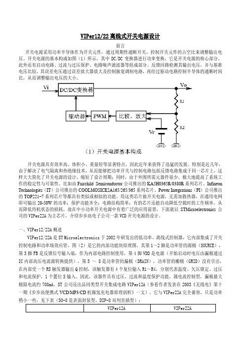
VIPer12/22离线式开关电源设计前言开关电源采用功率半导体作为开关元件,通过周期性通断开关,控制开关元件的占空比来调整输出电压。
开关电源的基本构成如图(1)所示,其中DC/DC变换器进行功率变换,它是开关电源的核心部分,此外还有启动电路、过流与过压保护、电路噪声滤波器等组成部分。
反馈回路检测其输出电压,并与基准电压比较,其误差电压通过误差放大器放大及控制脉宽调制电路,再经过驱动电路控制半导体的通断时间比,从而调整输出电压的大小。
开关电源具有效率高、体积小、重量轻等显著特点,因此近年来获得了迅猛的发展。
特别是近几年,由于解决了电气隔离和热绝缘技术,从而能够把功率开关与控制电路包括反馈电路集成于同一芯片上,这样大大简化了开关电源的设计、缩短了设计周期;同时,由于外围所需元器件很少,极大地提高了系统工作的稳定性与可靠性。
比如由Fairchild Semiconductor公司推出的KA5H0365R/0380R系列芯片、Infineon Technologies(IT)公司推出的COOLMOSICE2A165/265/365系列芯片、Power Integrations(PI)公司推出的TOP221~7系列芯片等都具有类似或相似的功能。
用这类芯片做开关电源,无需加散热器,在通用电网即可输出20-50W的功率;保护功能齐全;电路结构简单;有的芯片还能自动降低空载时的工作频率,从而降低待机状态的损耗,故在中小功率开关电源中有着广泛的应用前景,下面就以STMicroelectronics公司的VIPer22A为主芯片,介绍步步高电子公司一款VCD开关电源的设计。
一、VIPer12/22A概述VIPer12/22A是ST Microelectronics于2002年研发出的低功率、离线式控制器,它内部集成了开关控制电路和功率场效应管,图(2)是它的内部功能块原理图,其第1~2脚是功率管的源极(SOURCE),第3脚FB是反馈信号输入端,作为内部电路控制使用,第4脚VDD是电源(开始启动时电压由漏极通过IC内部高压电流源转换提供),第5 ~ 8是功率管的漏极(DRAIN),功率管的栅极(GRID)没有引出,在内部受一个RS触发器输出Q控制,该触发器有4个复位输入R1~R4,分别代表温度、欠压锁定、过压和电流保护,1个置位S输入。
替换进口VIP22的高性比电源驱动方案芯片VIPer22A

VOUT
R5 R6 2.5V R6
R3、R4 限制 U2 光耦 PC817B 的电流,避免影响反馈回路。C8 的加入使得系统反馈更加稳定,避免振荡。 VDD 电压部分
VIPer22A芯片工作电压范围宽,达到 9V——39V,此特性可以很方便的应用在某些特殊的领域,比如电池充
电器等。 当开关电源启动后,C2 电容上的电压会通过 T2 原边线圈、芯片内部的高压启动 MOS 管向芯片 VDD 电容 C4 充电。当 C4 电容电压达到 16V,内部高压启动 MOS 管关闭,同时 PWM 开启,系统开始工作。 当 C4 电容电压下降到 9V 以下,关闭 PWM 信号,同时芯片将会产生复位信号,使系统重新启动。这就是 欠压保护。
增加独立散热片; 其他散热措施。
典型示意电路图
AC
EMI Filter
Vou+
Vout-
1
GND
DRAIN
8
2
GND
DRAIN
7
VIPer22A
3
FB
DRAIN
6
4
VDD
DRAIN
5
-1-
VIPer22A AC/DC PWM 功率开关 V1.6
内部方框图
管脚说明
名称 GND FB VDD DRAIN 管脚序号 1,2 3 4 5,6,7,8 管脚说明 芯片地,同时也是内置高压 MOS 管 SOURCE 端口 反馈输入端口 芯片电源端,工作电压范围可达 9V—39V 内置高压 MOS 管的 DRAIN,同时芯片启动时,也做芯片的启动
-2-
VIPer22A AC/DC PWM 功率开关 V1.6
极限参数
极限参数(TA= 25℃) 符号 VDS(max) VDS(ST) VDD Ivdd IFB VESD TJ TSTG 说明 芯片 DRAIN 脚最高耐压 芯片启动时,DRAIN 脚最高耐压 芯片电源电压 嵌位电流 最大反馈电流 ESD 电压 结温 存储温度 范围 -0.3~730 -0.3~400 -0.3~39 10 3 >4000 -40~150 -55~150 单位 V V V mA mA V ℃ ℃
开关电源viper22a工作原理
viper22a工作原理开关电源具有效率高的特性,而且开关电源的变压器体积比串联稳压型电源的要小得多,电源电路比较整洁,整机重量也有所下降,所以,现在的DVD机大都使用开关电源。
电源电路正常是DVD机正常工作的基本保障。
1.开关电源的基本工作原理开关电源的结构框图如图1。
由对输出电压“取样”,并对基准源进行“比较”后控制“调整管”或“开关管”,此时开关电源的“开关管”相当于一个开关,开通时间由比较结果而定;当开关电源输出的电压太低时,通过“比较放大”控制“开关时间控制电路”使“开关管”开通时间变长,从而使输出的电压提升。
开关电源的核心部分是“开关管”和“变换器”组成的开关式直流-直流变换器。
它把直流电压Ui(一般由输入市电经整流、滤波后获得)经开关管后变为有一定占空比的脉冲电压Ua,然后经整流滤波后得到输出的电压Uo。
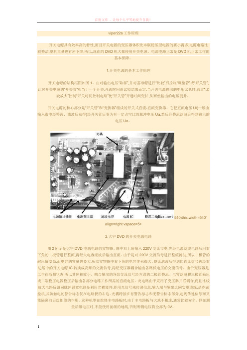
540)this.width=540"align=right vspace=5>2.大宇DVD的开关电源电路图2所示是大宇DVD电源电路的实物图。
图中右上角输入220V交流市电,先经电源滤波电路后用右下角的二极管进行整流,再经大电容滤波后输出直流。
由于是对220V交流信号进行整流滤波,所以二极管的耐压值要高,而电容的容量也要大,所以实物图中右下角的电容体积很大。
整流滤波后得到的直流信号再经右边居中的开关电源IC转换成高频的交流信号,再经变压器耦合输出各路低电压的交流信号。
由于变压器是工作在高频状态,所以其体积较小。
耦合输出的各组交流信号经左边的二极管整流、电容滤波和三极管稳压或三端稳压电源稳压后输出各部分电路工作所需的直流电压。
此电路由于采用了变压器并联耦合,而且比较放大电路反馈回脉冲调宽电路是利用光耦器件,即用光信号来传递信息,输入端与输出之间实现绝缘,是冷底盘机,其防触电的警告标志仅在电路板的右边。
光耦跨接在有警告标志和无警告标志部分,起到传递信号而又能隔离前后级地线的作用。
采纳VIPer22A的10W开关电源

采纳VIPer22A的10W开关电源2007-11-22 12:28:04 阅读272 评论0 字号:大中小定阅新型空调机采纳两个主低压输出给内部电子设备供电。
这两个主输出的低压由一个内部开关电源产生,它们别离是+12V和+5V。
那个开关电源应该具有效率高、重量轻、尺寸小、待机功耗低等特性。
本文介绍了利用VIPerX2系列产品开发的含有所有这些重要功能的电源实例。
目前,新型空调机采纳两个主低压输出给内部电子设备供电。
这两个主输出的低压别离是+12V和+5V。
低输出电压是由一个内部开关电源产生。
那个开关电源需要以下多个重要特性∶效率高,重量轻,尺寸小,待机功耗低等。
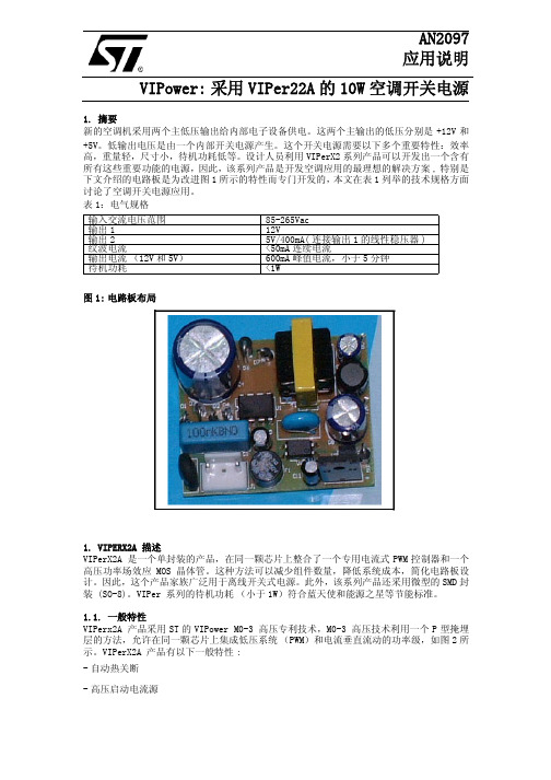
设计人员利用VIPerX2系列产品能够开发出一个含有所有这些重要功能的电源,因此,该系列产品是开发空调应用的最理想的解决方案, 专门是本文介绍的电路板是为改良图1所示的特性而专门开发的,表1列举了空调开关电源的技术规格。
表1∶电气规格图1: 电路板布局1. VIPERX2A描述VIPerX2A 是一个单封装的产品,在同一颗芯片上整合了一个专用电流式PWM操纵器和一个高压功率场效应MOS晶体管。
这种方式能够减少组件数量,降低系统本钱,简化电路板设计。
因此,那个产品家族普遍用于离线开关式电源。
另外,该系列产品还采纳微型的SMD 封装(SO-8)。
VIPer系列的待机功耗(小于1W)符合蓝天使和能源之星等节能标准。
1.1. 一般特性VIPerx2A产品采纳ST的VIPower M0-3高压专利技术,M0-3高压技术利用一个P型掩埋层的方式,许诺在同一颗芯片上集成低压系统(PWM)和电流垂直流动的功率级,如图2所示。
VIPerX2A产品有以下一样特性∶自动热关断;高压启动电流源;避免输出短路致使击穿故障的打嗝(HICCUP)模式;保证低负载条件下低功耗的突发模式。
而且,VIPower M0-3技术还可用于开发最小击穿电压为730V的功率场效应MOS晶体管。
VIPER-22A资料及原理图
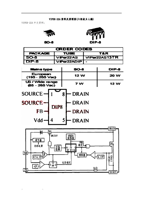
VIPER-22A资料及原理图(六祖故乡人编) VIPER-22A中文资料:黑表笔(脚)红表笔(脚)电阻(Ω)1、22、1 01、2 3 1.1k1、2 4 4.4k1、2 5、6、7、8 3.7k3 1、2 1.1k3 4 6.1k3 5、6、7、8 5.2k4 1、2 11k4 3 12.8k4 5、6、7、8 5k5、6、7、8 1、2 120k 5、6、7、8 3 125k 5、6、7、8 4 140kV IPER22A芯片概述:意法半导体的V IPER22A芯片为专用开关电源集成电路。
其部结构如图1所示。
芯片工作时, 直流电压从漏极脚进入集成电路, 经整流和稳压后供给开关电源工作, 从而使这个电路工作时不需要外接启动电阻。
即使VDD供电电路不正常, 电源电路的振荡电路仍能起振, 而且上图1 V IPER22A芯片部结构电路有输出电压。
在VDD正常前, 由芯片部自身供电, 经过很短时间后, VDD 供电电源正常, 此时,利用门电路控制开关电路(ON /OFF)断开从栅极输入的供电回路。
V IPER22A 有过热、过压保护功能。
VDD从4脚输入后, 首先送入比较器, 一旦输入VDD ≥42 V, 则触发器( FF1)输出一个置位信号1使控制振荡电路工作的触发器( FF2)输出为0,锁住U2 , 振荡信号无法输出, 即开关管不工作。
当输入电压小于1415 V时, U3 也将输出一个复位脉冲, 使开关管不工作。
当电路过热时, R1 为1,将FF2置0, 开关管不工作。
当供电电压VDD在正常围时, FB所得的取样电压与基准电压0123 V相比较, 用其比较结果去控制FF2 的转换频率,从而控制开关管的状态转换, 实现控制输出电压,达稳压的功能。
该集成电路芯片部包含60kHz的振荡电路, 其外围电路相当简单。
3 V IPER22A开关电源电路本文所使用的V IPER22A芯片具有优良的控制功能, 使得外围电路的设计较简单, 只需考虑一般的短路、过载电路保护即可。
buckboost电路区别?

Buck(降压)和Boost(提升)是两种常见的DC-DC 转换电路,它们具有不同的电压转换功能和特点。
Buck(降压)电路:
- 降压电路主要用于将输入电压降低到较低的输出电压,因此也被称为降压转换器。
- 降压电路的工作原理是通过控制开关管的导通时间比例,使得输入电压经过电感和电容的作用,转换为较低的输出电压。
- 降压电路的输出电压通常小于输入电压,用于供电给电压较低的设备或电路。
Boost(提升)电路:
- 提升电路主要用于将输入电压提高到较高的输出电压,因此也被称为升压转换器。
- 提升电路的工作原理是通过控制开关管的导通时间比例,使得输入电压经过电感和电容的作用,转换为较高的输出电压。
- 提升电路的输出电压通常大于输入电压,用于供电给电压较高的设备或电路。
区别:
1. **电压转换方向**:降压电路将输入电压降低到输出电压,
而提升电路将输入电压提升到输出电压。
2. **适用场景**:降压电路常用于需要输出低电压的场合,如电子设备的供电;提升电路常用于需要输出高电压的场合,如闪光灯、高压驱动器等。
3. **电路结构**:降压电路和提升电路在电路拓扑结构上有所不同,分别采用不同的开关管导通方式和电感电容的配置。
需要注意的是,除了降压和提升电路以外,还有一种称为Buck-Boost(升降压)的电路结构,它可以实现输入电压到输出电压的升降转换功能,更加灵活适用于各种电源管理系统的场合。
国产VIPer22A参考资料

VFB=2V; ID=1mA VFB=2V; VDS=500V ID=0.2A
IFB=2.0mA IFB=0.5mA;ID=50mA VDS=100V; VDD=5V
VFB=0V ID=0mA
最小 730
13 7 -
范围 典型
12 14.5 8 6.5 32 0.4 1.0 -220 60 560 700 0.9 1.23 300 700 150 30
业务电话:400-033-6518
-2-
sale@
Linkage
深圳市钲铭科电子有限公司
极限参数
极限参数(TA= 25℃)
符号
说明
VDS(max)
芯片 DRAIN 脚最高耐压
VDS(ST)
芯片启动时,DRAIN 脚最高耐压
VDD
芯片电源电压
深圳市钲铭科电子有限公司
电路图说明
上图中 D1-D4、C2 组成全波整流,D6、R1、C3 组成 RCD 吸收回路,消除变压器 T2 漏感产生的尖峰电压,
避免击穿 LKVIPER 22A 内部的高压 MOS 管。
输出部分 U3、U2、R5、R6、R3、R4、C8 组成采样反馈电路,R5、R6 决定系统的输出电压,输出电压 VOUT
Linkage
深圳市钲铭科电子有限公司
LKVIPER 22A
特点
85Vac~265Vac 宽电压输入 待机功耗小于 120mW@220Vac 集成高压启动电路 集成高压功率开关 60KHz 固定开关频率 9V~30V 宽 VDD 工作电压范围 电流模式 PWM 控制方式 内置过温、过流、过压、欠压
R7
33K
RT1
5D-9
基于Viper22的单端反激式开关电源设计

基于Viper22的单端反激式开关电源设计
张久亮;郭前岗;周西峰
【期刊名称】《电源技术》
【年(卷),期】2014(038)009
【摘要】设计了一种以Viper22为PWM控制芯片的高频单端反激式开关电源.利用三端稳压器TL431和光耦隔离器件PC817实现了对电源电压的隔离、反馈以及控制.这是一款输入交流电压范围为85~265 V,输出直流电压为15 V/0.4A和9 V/0.5 A的单端反激式开关电源,具有体积小,功率密度高等优点,适用于基于单片机的逆变系统.实验结果表明,所设计的开关电源具有优良的稳压性能,输出电压纹波小.目前,该开关电源已运用于基于单片机的无刷直流电机控制系统一年多,运行稳定.【总页数】3页(P1733-1734,1761)
【作者】张久亮;郭前岗;周西峰
【作者单位】南京邮电大学,江苏南京210046;南京邮电大学,江苏南京210046;南京邮电大学,江苏南京210046
【正文语种】中文
【中图分类】TM591
【相关文献】
1.基于OB2273的单端反激式开关电源设计 [J], 韩召成;文定都;胡正国;任于涵
2.基于UC3842芯片的单端反激式开关电源设计 [J], 赵志敏;
3.基于TO P227 Y的多输出单端反激式开关电源设计 [J], 高佳;倪怀洲;王旭光;万
国超;刘贵彬
4.基于LT1244的单端反激式开关电源设计 [J], 谢秀镯;张云鹏;田志
5.基于UC3842的单端反激式开关电源设计 [J], 王秋妍;郑浩;王道平;王凯;
因版权原因,仅展示原文概要,查看原文内容请购买。
VIPER-22A资料及原理图解读
VIPER-22A资料及原理图(六祖故乡人编) VIPER-22A中文资料:HR500-2型万能表R×1kΩ档估测的内阻值:黑表笔(脚)红表笔(脚)电阻(Ω)1、22、1 01、2 3 1.1k1、2 4 4.4k1、2 5、6、7、8 3.7k3 1、2 1.1k3 4 6.1k3 5、6、7、8 5.2k4 1、2 11k4 3 12.8k4 5、6、7、8 5k5、6、7、8 1、2 120k5、6、7、8 3 125k5、6、7、8 4 140kV IPER22A芯片概述:意法半导体的V IPER22A芯片为专用开关电源集成电路。
其内部结构如图1所示。
芯片工作时, 直流电压从漏极脚进入集成电路, 经整流和稳压后供给开关电源工作, 从而使这个电路工作时不需要外接启动电阻。
即使VDD供电电路不正常, 电源电路的振荡电路仍能起振, 而且上图1 V IPER22A芯片内部结构电路有输出电压。
在VDD正常前, 由芯片内部自身供电, 经过很短时间后, VDD供电电源正常, 此时,利用门电路控制开关电路(ON /OFF)断开从栅极输入的供电回路。
V IPER22A 有过热、过压保护功能。
VDD从4脚输入后, 首先送入比较器, 一旦输入VDD ≥42 V, 则触发器( FF1)输出一个置位信号1使控制振荡电路工作的触发器( FF2)输出为0,锁住U2 , 振荡信号无法输出, 即开关管不工作。
当输入电压小于1415 V时, U3 也将输出一个复位脉冲, 使开关管不工作。
当电路过热时, R1 为1,将FF2置0, 开关管不工作。
当供电电压VDD在正常范围时, FB所得的取样电压与基准电压0123 V相比较, 用其比较结果去控制FF2 的转换频率,从而控制开关管的状态转换, 实现控制输出电压,达稳压的功能。
该集成电路芯片内部包含60kHz的振荡电路, 其外围电路相当简单。
3 V IPER22A开关电源电路本文所使用的V IPER22A芯片具有优良的控制功能, 使得外围电路的设计较简单, 只需考虑一般的短路、过载电路保护即可。
viper22 (2)
Viper22IntroductionThe Viper22 is a high voltage converter IC designed for driving high power LEDs, as well as lamps and other non-isolated low voltage applications. It is manufactured by STMicroelectronics, a leading semiconductor company.Features•High voltage start-up current source•PWM operation with frequency up to 130kHz•Embedded protection functions (over-temperature, over-voltage, and over-current)•Low standby power consumption•Wide input voltage range (8V to 35V)•Output current up to 300mA•Adjustable output voltagePin ConfigurationThe Viper22 is available in an 8-pin DIP package with the following pin configuration: 1. Ground (GND) 2. Feedback (FDBK) 3. Drain (DRAIN) 4. Output Voltage Sense (VSENSE) 5.Output Voltage Set (VSET) 6. Soft-start (SS) 7. Input Voltage Sense (VSENSE) 8. Supply Voltage (VIN)Working PrincipleThe Viper22 operates by using a flyback converter topology. It controls the switching of an external MOSFET to deliver output power to the load. The switching frequency can be adjusted using an external resistor connected to the FDBK pin. The high voltage start-up current source provides the initial power needed to start the converter.The IC includes protection functions to ensure safe operation. The over-temperature protection shuts down the converter in case the temperature exceeds a certain threshold. The over-voltage and over-current protections prevent the output voltage and current from exceeding their maximum limits, respectively.The VSENSE pins are used for feedback and sensing the output voltage. The VSET pin is used to adjust the output voltage level. The SS pin provides a soft-start function to gradually ramp up the output voltage when the converter is powered on.Application CircuitTo use the Viper22, an application circuit as shown below can be implemented:+-------------+| |+---| VIN || | || +--|\\\\|--|+--|+| | | | || --- --- ---| | | || +---| | || | | | || | | /|\\ || | --- --- || | | | || +----|___|__|| F | |+----------|__||+----|\\/|----+| |/\\| || || Viper22 || |+---|/\\|-----+| ||--- LampThis circuit demonstrates the connection of the Viper22 to a load, such as a lamp or an LED. The VIN pin is connected to the power supply, while the VOUT pin is connected to the load. The feedback resistor RFB is used to adjust the output voltage level according to the desired application.ConclusionThe Viper22 is a versatile high voltage converter IC suitable for driving high power LEDs and non-isolated low voltageapplications. With its features such as adjustable output voltage, embedded protection functions, and low standby power consumption, it offers a reliable and efficient solution for various lighting applications. The provided application circuit serves as a reference for implementing the Viper22 in practical scenarios.Please note that this document provides a brief overview of the Viper22 and its application. For detailed information regarding the electrical characteristics, design guidelines, and safety precautions, refer to the official datasheet provided by STMicroelectronics.。
12 18W电源芯片VIPer 22A

VOUT =
R5 + R6 × 2.5V R6
R3、R4 限制 U2 光耦 PC817B 的电流,避免影响反馈回路。C8 的加入使得系统反馈更加稳定,避免振荡。 � VDD 电压部分 LKVIPER 22A 芯片工作电压范围宽,达到 9V——30V,此特性可以很方便的应用在某些特殊的领域,比如电 池充电器等。 当开关电源启动后, C2 电容上的电压会通过 T2 原边线圈、芯片内部的高压启动 MOS 管向芯片 VDD 电容 C4 充电。当 C4 电容电压达到 16V,内部高压启动 MOS 管关闭,同时 PWM 开启,系统开始工作。 当 C4 电容电压下降到 9V 以下,关闭 PWM 信号,同时芯片将会产生复位信号,使系统重新启动。这就是 欠压保护。
GND
V out out-
1 2 3 4
8 D R A IN 7 D R A IN 6 D R A IN 5 D R A IN
电源
GND FB VDD
LKVIPER 2 2 A
-1-
深圳市钲铭科电子有限公司 内部方框图
VIPer22A 芯片(12-18W) LED 电源方案
DRAI N VDD 内部电源 产生电路 LVDD 基准电路 VREF
ID
VF B =0
ID L IM
IFB = -
0.23V F B IFB S D
从上图可以看出,IFB 电流大,ID 的电流就小;IFB 电流小,ID 的电流就大。当 IFB 的电流大于 IFBSD 时, 芯片会关闭 PWM,此时的 ID 的值大约为 85mA,同时芯片会自动进入突发模式。这对于系统工作在空载或者轻 载至关重要。 � 过压保护
-2-
深圳市钲铭科电子有限公司 极限参数
电磁炉电源芯片各引脚电压
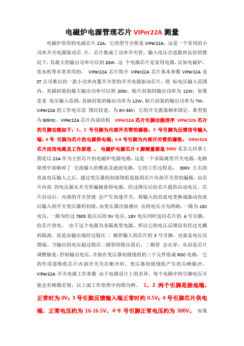
电磁炉电源管理芯片VIPer22A测量电磁炉常用的电源芯片22A,它的型号全称是VIPer22A,这是一个常用的小功率开关电源驱动芯片,芯片集成了功率开关管,输入电压合适散热良好的情况下,其最大的输出功率可以到20W。
这个电源芯片是家用电器,比如电磁炉、饮水机等非常常用的。
VIPer22A芯片简介VIPer22A芯片基本参数VIPer22A是ST公司推出的一款小功率内置开关管的开关电源驱动芯片,欧标电压输入范围内,直插封装的最大输出功率可以到20W,贴片封装的输出功率为12W;如果是宽电压输入范围,直插封装的输出功率为12W,贴片封装的输出功率为7W。
VIPer22A的工作电压范围比较宽,为9V-38V;它的开关震荡频率固定,典型值为60kHz。
VIPer22A芯片内部结构VIPer22A芯片引脚功能排序VIPer22A芯片的引脚功能如下:1、2号引脚为内部开关管的源极;3号引脚为反馈信号输入端;4号引脚为芯片的电源供电端;5-8号引脚为内部开关管的漏极。
VIPer22A 芯片应用电路及工作原理。
电磁炉电源芯片8脚测量都是300V是怎么回事上图是以22A作为主控芯片的电磁炉电源电路,这是一个非隔离型开关电源,电路原理中省略掉了交流输入的整流及滤波电路。
它的工作过程是:300V左右的直流电压输入之后,通过变压器的初级绕组连接到芯片内部开关管的漏极,由芯片内部的电压源从开关管漏极获得电源,经过降压后给芯片提供启动电压。
芯片启动后,内部的开关管就会产生高速开关,将输入的直流电变换成脉动直流后输入到开关变压器的初级,由变压器次级感应出的电压分为两路,一路为18V 电压,一路为经过7805稳压后的5V电压。
18V电压同时返回芯片的4号引脚,给芯片供电。
由于这个电源为非隔离型电源,所以它的电压反馈没有经过光耦的隔离,而是由输出端经过稳压二极管输入到芯片的3号引脚,也就是电压反馈端。
当输出的电压超过稳压二极管的稳压值后,二极管会击穿,从而是芯片调整脉宽,控制输出电压。
VIPER精选A及原理图
V I P E R-22A资料及原理图(六祖故乡人编) VIPER-22A中文资料:(六祖故乡人编)HR500-2型万能表R×1kΩ档估测的内阻值:(六祖故乡人编)(六祖故乡人编)(六祖故乡人编)VIPER22A芯片概述:意法半导体的VIPER22A芯片为专用开关电源集成电路。
其内部结构如图1所示。
芯片工作时,直流电压从漏极脚进入集成电路,经整流和稳压后供给开关电源工作,从而使这个电路工作时不需要外接启动电阻。
即使VDD供电电路不正常,电源电路的振荡电路仍能起振,而且上图1 VIPER22A芯片内部结构电路有输出电压。
在VDD正常前,由芯片内部自身供电,经过很短时间后,VDD供电电源正常,此时,利用门电路控制开关电路(ON/OFF)断开从栅极输入的供电回路。
VIPER22A有过热、过压保护功能。
VDD从4脚输入后,首先送入比较器,一旦输入VDD≥42V,则触发器(FF1)输出一个置位信号1使控制振荡电路工作的触发器(FF2)输出为0,锁住U2,振荡信号无法输出,即开关管不工作。
当输入电压小于1415V时,U3也将输出一个复位脉冲,使开关管不工作。
当电路过热时,R1为1,将FF2置0,开关管不工作。
当供电电压VDD在正常范围时,FB 所得的取样电压与基准电压0123V相比较,用其比较结果去控制FF2的转换频率,从而控制开关管的状态转换,实现控制输出电压,达稳压的功能。
该集成电路芯片内部包含60kHz的振荡电路,其外围电路相当简单。
3 VIPER22A开关电源电路本文所使用的VIPER22A芯片具有优良的控制功能,使得外围电路的设计较简单,只需考虑一般的短路、过载电路保护即可。
电路原理图如图2。
图2 电路原理图(下图)在交流电源的输入端接电容C0用于滤除低频差模噪声,接扼流圈用于过滤掉电网上的干扰,同时也滤掉电源对电网的干扰。
220V的交流电源输入后,(六祖故乡人编)经四个二极管构成的桥式整流电路整流,C1滤波后输出一个300V左右的直流信号。
非隔离型降压式电源设计方法
VIPer22A应用中文资料
AN2097应用说明VIPower:采用VIPer22A的10W空调开关电源1. 摘要新的空调机采用两个主低压输出给内部电子设备供电。
这两个主输出的低压分别是+12V和+5V。
低输出电压是由一个内部开关电源产生。
这个开关电源需要以下多个重要特性:效率高,重量轻,尺寸小,待机功耗低等。
设计人员利用VIPerX2系列产品可以开发出一个含有所有这些重要功能的电源,因此,该系列产品是开发空调应用的最理想的解决方案,特别是下文介绍的电路板是为改进图1所示的特性而专门开发的,本文在表1列举的技术规格方面讨论了空调开关电源应用。
表1:电气规格图1:电路板布局1. VIPERX2A 描述VIPerX2A 是一个单封装的产品,在同一颗芯片上整合了一个专用电流式PWM控制器和一个高压功率场效应MOS晶体管。
这种方法可以减少组件数量,降低系统成本,简化电路板设计。
因此,这个产品家族广泛用于离线开关式电源。
此外,该系列产品还采用微型的SMD封装 (SO-8)。
VIPer 系列的待机功耗(小于1W)符合蓝天使和能源之星等节能标准。
1.1. 一般特性VIPerx2A 产品采用ST的VIPower M0-3 高压专利技术,M0-3 高压技术利用一个P型掩埋层的方法,允许在同一颗芯片上集成低压系统(PWM)和电流垂直流动的功率级,如图2所示。
VIPerX2A 产品有以下一般特性:-自动热关断-高压启动电流源输入交流电压范围85-265Vac输出112V输出25V/400mA(连接输出1的线性稳压器)纹波电流<50mA连续电流输出电流(12V和5V)600mA峰值电流,小于5分钟待机功耗<1W-防止输出短路导致击穿故障的打嗝(HICCUP)模式-保证低负载条件下低功耗的突发模式而且,VIPower M0-3技术还可用于开发最小击穿电压为730V 的功率场效应MOS 晶体管。
表2说明了该产品在不同的封装和工作条件下的功率处理能力。
电源芯片viper22a工作原理

电源芯片viper22a工作原理开关电源具有效率高的特性,而且开关电源的变压器体积比串联稳压型电源的要小得多,电源电路比较整洁,整机重量也有所下降,所以,现在的DVD机大都使用开关电源。
电源电路正常是DVD机正常工作的基本保障。
1.开关电源的基本工作原理 开关电源的结构框图如图1。
由对输出电压“取样”,并对基准源进行“比较”后控制“调整管”或“开关管”,此时开关电源的“开关管”相当于一个开关,开通时间由比较结果而定;当开关电源输出的电压太低时,通过“比较放大”控制“开关时间控制电路”使“开关管”开通时间变长,从而使输出的电压提升。
开关电源的核心部分是“开关管”和“变换器”组成的开关式直流-直流变换器。
它把直流电压Ui(一般由输入市电经整流、滤波后获得)经开关管后变为有一定占空比的脉冲电压Ua,然后经整流滤波后得到输出的电压Uo。
图2所示是电源电路的实物图。
图中右上角输入220V交流市电,先经电源滤波电路后用右下角的二极管进行整流,再经大电容滤波后输出直流。
由于是对220V交流信号进行整流滤波,所以二极管的耐压值要高,而电容的容量也要大,所以实物图中右下角的电容体积很大。
整流滤波后得到的直流信号再经右边居中的开关电源IC转换成高频的交流信号,再经变压器耦合输出各路低电压的交流信号。
由于变压器是工作在高频状态,所以其体积较小。
耦合输出的各组交流信号经左边的二极管整流、电容滤波和三极管稳压或三端稳压电源稳压后输出各部分电路工作所需的直流电压。
此电路由于采用了变压器并联耦合,而且比较放大电路反馈回脉冲调宽电路是利用光耦器件,即用光信号来传递信息,输入端与输出之间实现绝缘,是冷底盘机,其防触电的警告标志仅在电。
DVD机VIPer22A开关电源工作原理分析
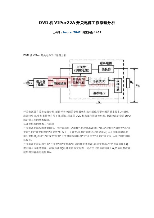
DVD机VIPer22A开关电源工作原理分析上传者:haoren7842浏览次数:1469DVD机VIPer开关电源工作原理分析开关电源具有效率高的特性,而且开关电源的变压器体积比串联稳压型电源的要小得多,电源电路比较整洁,整机重量也有所下降,所以,现在的DVD机大都使用开关电源。
电源电路正常是DVD 机正常工作的基本保障。
1.开关电源的基本工作原理开关电源的结构框图如图1。
由对输出电压“取样”,并对基准源进行“比较”后控制“调整管”或“开关管”,此时开关电源的“开关管”相当于一个开关,开通时间由比较结果而定;当开关电源输出的电压太低时,通过“比较放大”控制“开关时间控制电路”使“开关管”开通时间变长,从而使输出的电压提升。
开关电源的核心部分是“开关管”和“变换器”组成的开关式直流-直流变换器。
它把直流电压Ui(一般由输入市电经整流、滤波后获得)经开关管后变为有一定占空比的脉冲电压Ua,然后经整流滤波后得到输出的电压Uo。
2.大宇DVD的开关电源电路图2所示是大宇DVD电源电路的实物图。
图中右上角输入220V交流市电,先经电源滤波电路后用右下角的二极管进行整流,再经大电容滤波后输出直流。
由于是对220V交流信号进行整流滤波,所以二极管的耐压值要高,而电容的容量也要大,所以实物图中右下角的电容体积很大。
整流滤波后得到的直流信号再经右边居中的开关电源IC转换成高频的交流信号,再经变压器耦合输出各路低电压的交流信号。
由于变压器是工作在高频状态,所以其体积较小。
耦合输出的各组交流信号经左边的二极管整流、电容滤波和三极管稳压或三端稳压电源稳压后输出各部分电路工作所需的直流电压。
此电路由于采用了变压器并联耦合,而且比较放大电路反馈回脉冲调宽电路是利用光耦器件,即用光信号来传递信息,输入端与输出之间实现绝缘,是冷底盘机,其防触电的警告标志仅在电路板的右边。
光耦跨接在有警告标志和无警告标志部分,起到传递信号而又能隔离前后级地线的作用。
buckboost电路原理

buckboost电路原理Buck-boost电路原理。
Buck-boost电路是一种常见的直流-直流转换器电路,它可以实现输入电压的升压或降压,是许多电子设备中常用的电源管理电路。
本文将介绍buck-boost电路的原理及其工作方式。
首先,我们来看一下buck-boost电路的基本结构。
它由一个开关管、电感、二极管和电容组成。
在工作时,开关管周期性地开关,使得输入电压在电感和电容的作用下得到升压或降压,最终输出所需要的电压。
这种结构简单而有效,广泛应用于各种电子设备中。
其次,我们来了解一下buck-boost电路的工作原理。
在升压模式下,当开关管导通时,电感中储存的能量会被传递到输出端,从而实现输入电压的升压。
而在降压模式下,当开关管断开时,电感中的能量会继续流动,从而实现输入电压的降压。
通过控制开关管的导通和断开,可以实现输入电压到输出电压的灵活转换。
另外,buck-boost电路还有一些特点和应用。
首先,它具有高效率和快速响应的特点,能够满足各种电子设备对电源的要求。
其次,它还具有较宽的输入电压范围和输出电压范围,适用于不同的场合。
除此之外,buck-boost电路还可以用于电池充放电管理、LED驱动、太阳能电池系统等领域。
最后,我们来总结一下buck-boost电路的优缺点。
优点是它具有高效率、灵活性强、适用范围广等特点,能够满足各种电子设备的需求。
缺点是在设计和调试时需要考虑更多的因素,比如电感和电容的选择、开关管的选型等,因此需要一定的专业知识和经验。
综上所述,buck-boost电路是一种常见且实用的直流-直流转换器电路,它具有升压和降压的功能,适用于各种电子设备中。
通过对其原理和特点的了解,我们可以更好地应用和设计这种电路,满足不同场合的需求。
希望本文能够对您有所帮助,谢谢阅读!。
- 1、下载文档前请自行甄别文档内容的完整性,平台不提供额外的编辑、内容补充、找答案等附加服务。
- 2、"仅部分预览"的文档,不可在线预览部分如存在完整性等问题,可反馈申请退款(可完整预览的文档不适用该条件!)。
- 3、如文档侵犯您的权益,请联系客服反馈,我们会尽快为您处理(人工客服工作时间:9:00-18:30)。
AN2544Application noteDesigning a low cost power supply using aVIPer12/22A-E in a buck configurationIntroductionMany appliances today use nonisolated power supply to furnish low output power requiredto run a micro, LED display, and a few relays or AC switches. This type of power supply hasa single rectifier so as to reference the neutral to output ground in order to fire TRIACs or ACswitches. This article describes the use of the VIPer12A-E and the VIPer22A-E which arepin-for-pin compatible and can supply power for many applications. This paper provides anoff-line, nonisolated power supply evaluation board based on the VIPer12/22A-E. Fourdifferent examples are covered. The VIPer12A-E is used for 12 V at 200 mA and 16 V at 200mA. The VIPer22A-E is used for 12 V at 350 mA and 16 V at 350 mA. The same board canbe used for any output voltage from 10 V to 35 V. For outputs less than 16 V, D6 and C4 arepopulated and W1 is omitted. For outputs greater than 16 V, D6 and C4 are omitted and W1is populated. For more design detail, see AN1357 "VIPower: low cost power sullies usingthe VIPer12A-E in nonisolated application." The objective of this application note is tofamiliarize the end user with this reference design and to quickly modify it for differentvoltage output. This design gives:■Lowest possible component count■Integrated thermal overload protection■About 200 mW at no-load consumption■Efficiency measured between 70% to 80% at full load■Integrated Short circuit protectionFigure 1.Evaluation board (STEVAL-ISA035V1)Table 1.Operating conditions for the four samplesBoard version (with changes)Output voltage and currentInput voltage range85 V ac to 264 V acInput voltage frequency range50/60 HzOutput version 1 VIPer22ADIP-E12 V at 350 mA 4.2 WOutput version 2 VIPer12ADIP-E12 V at 200 mA 2.4 WOutput version 3 VIPer22ADIP-E16 V at 350 mA 5.6 WOutput version 4 VIPer12ADIP-E16 V at 200 mA 3.2 WNovember 2007Rev 4 1/17Contents AN2544 Contents1Circuit operation . . . . . . . . . . . . . . . . . . . . . . . . . . . . . . . . . . . . . . . . . . . . 41.1Input line rectification and line conducted filter . . . . . . . . . . . . . . . . . . . . . . 41.2Start circuit . . . . . . . . . . . . . . . . . . . . . . . . . . . . . . . . . . . . . . . . . . . . . . . . . 41.3Inductor selection . . . . . . . . . . . . . . . . . . . . . . . . . . . . . . . . . . . . . . . . . . . . 51.4Design example . . . . . . . . . . . . . . . . . . . . . . . . . . . . . . . . . . . . . . . . . . . . . 51.5Design hints and trade-off . . . . . . . . . . . . . . . . . . . . . . . . . . . . . . . . . . . . . 51.6Board layout . . . . . . . . . . . . . . . . . . . . . . . . . . . . . . . . . . . . . . . . . . . . . . . . 91.7Burst mode in no-load or very light load . . . . . . . . . . . . . . . . . . . . . . . . . . 111.8Short circuit . . . . . . . . . . . . . . . . . . . . . . . . . . . . . . . . . . . . . . . . . . . . . . . 121.9Performance . . . . . . . . . . . . . . . . . . . . . . . . . . . . . . . . . . . . . . . . . . . . . . . 131.10EMI conducted . . . . . . . . . . . . . . . . . . . . . . . . . . . . . . . . . . . . . . . . . . . . . 15 2Conclusion . . . . . . . . . . . . . . . . . . . . . . . . . . . . . . . . . . . . . . . . . . . . . . . . 16 3Revision history . . . . . . . . . . . . . . . . . . . . . . . . . . . . . . . . . . . . . . . . . . . 162/17AN2544List of figures List of figuresFigure 1.Evaluation board (STEVAL-ISA035V1) . . . . . . . . . . . . . . . . . . . . . . . . . . . . . . . . . . . . . . . . 1 Figure 2.Inductor current: 470 µH VS 1000 µH. . . . . . . . . . . . . . . . . . . . . . . . . . . . . . . . . . . . . . . . . . 6 Figure 3.Schematic for 12 V at 350 mA . . . . . . . . . . . . . . . . . . . . . . . . . . . . . . . . . . . . . . . . . . . . . . . 7 Figure 4.Schematic for 16 V at 350 mA . . . . . . . . . . . . . . . . . . . . . . . . . . . . . . . . . . . . . . . . . . . . . . . 8 Figure posite. . . . . . . . . . . . . . . . . . . . . . . . . . . . . . . . . . . . . . . . . . . . . . . . . . . . . . . . . . . . . . . 9 Figure 6.Top side . . . . . . . . . . . . . . . . . . . . . . . . . . . . . . . . . . . . . . . . . . . . . . . . . . . . . . . . . . . . . . . . 9 Figure 7.Bottom side and surface mount components (viewed from top). . . . . . . . . . . . . . . . . . . . . . 9 Figure 8.Bad start. . . . . . . . . . . . . . . . . . . . . . . . . . . . . . . . . . . . . . . . . . . . . . . . . . . . . . . . . . . . . . . 11 Figure 9.Good start. . . . . . . . . . . . . . . . . . . . . . . . . . . . . . . . . . . . . . . . . . . . . . . . . . . . . . . . . . . . . . 11 Figure 10.Burst mode. . . . . . . . . . . . . . . . . . . . . . . . . . . . . . . . . . . . . . . . . . . . . . . . . . . . . . . . . . . . . 12 Figure 11.Operation during a short. . . . . . . . . . . . . . . . . . . . . . . . . . . . . . . . . . . . . . . . . . . . . . . . . . . 12 Figure 12.Load regulations for 12 V output. . . . . . . . . . . . . . . . . . . . . . . . . . . . . . . . . . . . . . . . . . . . . 14 Figure 13.Line regulation . . . . . . . . . . . . . . . . . . . . . . . . . . . . . . . . . . . . . . . . . . . . . . . . . . . . . . . . . . 14 Figure 14.Efficiency . . . . . . . . . . . . . . . . . . . . . . . . . . . . . . . . . . . . . . . . . . . . . . . . . . . . . . . . . . . . . . 15 Figure 15.VIPer22-E, 12 V at 350 mA output. . . . . . . . . . . . . . . . . . . . . . . . . . . . . . . . . . . . . . . . . . . 15 Figure 16.VIPer12-E, 12 V at 200 mA output. . . . . . . . . . . . . . . . . . . . . . . . . . . . . . . . . . . . . . . . . . . 15 Figure 17.VIPer22-E, 16 V at 350 mA output. . . . . . . . . . . . . . . . . . . . . . . . . . . . . . . . . . . . . . . . . . . 16 Figure 18.VIPer12-E, 16 V at 200 mA output. . . . . . . . . . . . . . . . . . . . . . . . . . . . . . . . . . . . . . . . . . . 163/17Circuit operation AN25444/171 Circuit operation1.1Input line rectification and line conducted filterThe circuit operations for all four versions are basically the same. The difference is in thecircuit for startup. Version 1 will be described here with reference to Figure 3. The output of the converter is not isolated from the input. This makes neutral common to output ground thus giving a reference back to neutral. The buck is less expensive due to the fact that it does not use a transformer and an opto coupler. The AC line is applied through D1 which rectifies the line input every other half cycle.C1, L0, C2 form a pie filter to reduce EMI noise. The value of the capacitor is chosen to maintain a reasonable valley, because the caps are charged every other half cycle. Two diodes can be used in place of D1 to sustain burst pulses of 2 kV . R10 serves two purposes, one is for inrush limiting and the other is to act as a fuse in case of a catastrophic failure. A wire wound resistor handles the energy of the inrush. Flame proof resistor and a fuse can be used depending on system and safety requirements. C7 helps the EMI by balancing line and neutral noise without using an Xcap. This will pass EN55022 level "B". If the requirement is less, then this cap can be left out of the circuit.1.2 Start circuitThe voltage across C2 is fed to the drain, pin 5 through 8. Inside the VIPer, the constantcurrent source delivers 1mA to the V dd pin 4. This current charges C3. When the voltage on the V dd pin reaches 14.5 V nominal, the current source turns off and the VIPer startspulsing. During this time, the energy is being supplied from the V dd cap. The energy stored must be greater than the energy needed to supply the output current plus the energy to charge of the output capacitor, before the V dd cap falls below 9 V . This can be seen in Figure 8 and Figure 9. The value of the capacitor is therefore chosen to accommodate the startup time. During a short circuit, the V dd cap discharges below the minim value enabling the internal high voltage current generator to initiate a new startup sequence. The charging and discharging of the capacitor determine the time period that the power supply is to be on and off. This reduces the RMS heating effect on all components. The regulation circuit consists of Dz, C4 and D8. D8 peak charges C4 during the freewheeling time when D5 is conducting. During this time, the source or reference to the VIPer is one diode drop below ground, which compensates for the D8 drop. So basically the Zener voltage is the same as the output voltage. C4 is connected across V fb and source to filter the regulation voltage. Dz is a BZT52C12, ½ W Zener with a specified test current of 5 mA. These Zeners that are specified at a lower current give better accuracy of the output voltage. If the output voltage is lower than 16 V, the circuit can be configured as in Figure 3 where V dd is separated from the V fb pin. When the internal current source charges the V dd cap, V dd can reach 16V at worse case condition. A 16 V Zener with a 5% low tolerance can be 15.2 V plus the internal resistance to ground is 1230 Ω which is an additional 1.23 V for a total of 16.4 V . For 16 V output and higher, the V dd pin and the V fb pin can share a common diode and capacitor filter similar to Figure 4.AN2544Circuit operation5/171.3 Inductor selectionA starting point for the inductor operating in discontinuous mode can be derived from thefollowing formula which gives a good approximation of the inductor.Equation 1Where Id peak is the minimum peak drain current, 320 mA for the VIPer12A-E and 560 mA for the VIPer22A-E, f is the switching frequency at 60 kHz. The maximum peak current limits the power delivered in the buck topology. Therefore, the calculation above is for an inductor that operates in discontinuous mode. If the current swings down to zero, than the peak current is twice the output. This limits the output current to 280 mA for a VIPer22A-E. If the inductor is a larger value, operating between continuous and discontinuous mode, we can reach 200 mA comfortably away from the current limit point. C6 has to be a low ESR capacitor to give the low ripple voltage Equation 2D5 needs to be a fast recovery diode but D6 and D8 can be standard diodes. DZ1 is used to clamp the voltage to 16 V . The nature of the buck topology is to peak charge at no-load. A Zener 3 to 4 V higher than the output voltage is recommended.1.4 Design exampleFigure 3 is the schematic for the evaluation board. It is set up for 12 V with a maximumcurrent of 350 mA. If less current is required, then the VIPer22A-E can be changed to a VIPer12A-E and C2 can be decreased from 10 µf to 4.7 µF . This delivers up to 200 mA. Figure 4 shows the same board but for 16 V output or higher, D6 and C4 can be left out. The jumper bridges the output voltage to the V dd pin.1.5 Design hints and trade-offThe value of L determines the boundary condition between continuous and discontinuous mode for a given output current. In order to operate in discontinuous mode, the inductor value has to be lower than Equation 3Where R is the load resistance, T is the switching period, and D is the duty cycle.There are two points to consider. One is, the more discontinuous the higher the peakcurrent. This point should be kept lower than the minimum pulse by pulse current limit of the VIPer22A-E which is 0.56 A. The other is if we use a larger value inductor to run continuous all of the time, we run into excess heat from switching losses of the MOSFET inside the VIPer. Of course, the inductor current rating must be higher than the output current to prevent the risk of saturating the core.L 2Pout Id peak ()2f•-------------------------------•=V ripple I ripple Cesr•=L 12--R T 1D –()•••=Circuit operation AN25446/17Figure 2.Inductor current: 470 µH VS 1000 µHThe blue trace is the current with 470 µH inductor and the purple trace is the current with a 1000 µH inductor.On the above scope plot in Figure2, the trace represents the current going through the inductor. Current charges up the inductor during the time the MOSFET is on. At this time, the source pin is the same as the rectified line input and the current is ramping up. At 350 mA output current, the peak of the current is 550 mA for a 470 µH inductor, the blue trace. The worse case condition for the VIPer Idlim is 560 mA. So therefore we are close to the pulse by pulse current limit trip point. This is manifested by the output voltage dropping as the output current is being raised past the limit. 470 µH inductor is the minimum value that can be used from the calculations for a 350 mA output. A good compromise is a 1000 µH making the swing less, keeping the peak at 443 mA, away from the 560 mA current limit. Looking at the purple trace the turn-on losses are increased and the turn-off losses are decreased in the MOSFET inside the VIPer.It is best to choose the inductor to give ½ the ripple current between discontinuous to continuous. This is the best compromise when working close to the maximum current. The trade-off is a little more heat for the safety margin away from the current trip point.VIPer temperature rise with two different inductors at 350 mA is:Table 2.VIPer temperature rise with different inductorsInductor Maximum peak current VIPer22ADIP-E temperature rise470 µH550 mA34 °C1000 µH443 mA40.5 °CAN2544Circuit operation7/17Circuit operation AN25448/17AN2544Circuit operation9/171.6 Board layoutA composite view of the board shows a double-sided board with surface mount componentson the bottom. The top is a ground plane which helps with EMI. The actual measurements of the PC board are 55 mm by 23 mm.Figure 5.CompositeFigure 6.Top sideFigure 7.Bottom side and surface mount components (viewed from top)Circuit operation AN254410/17The above board can be modified to any voltage output from 10 V to 15 V by changing DZ. To modify the board to 16 or higher, D6 and C4 can be omitted and the jumper wire can be installed. For 16 V operation or higher, V dd and Vf can share the same source without having the current leak through the Zener and Vf pin path. The output voltage can be changed by changing DZ from 16 V Zener to a higher value matching the output voltage. If less current is required, the board can be changed with a VIPer12A-E dip which is pin-for-pin compatible with the VIPer22ADIP-E.Also one of the input capacitors, C2, can be reduced to 4.7 µF. Various data and waveforms from evaluation boards can be seen in the following pages.The V dd cap has to be sized according to the output load and the size of the output capacitor.Table 3.Bill of material for VIPer22A-E Buck 12 V at 350 mAItem Qty Ref.Part V/W Description CAT# 11Cx0.02250 V X7R +/-10%GP SM Ceramic22C1,C210 µF400 V105 CUCCEKMG401ELL100MJ20S31C3 4.7 µF25 V X7R +/-10%TDK C3216X7R1E475K 41C40.47 µF25 V X7R +/-10%TDK C2012X7R1E474K 51C647 µF50 V105 C Low ESR Low ESR61C70.1 µ 1 kV X7R +/-15%MurataGRM55DR73A104KW01171DZ12 V zener BZT5212FDICT 81DZ116 V zener BZT5216FDICT 93D1,D6,D8S1MDICT SM GP Diode 1 kV 1 A S1MD101D5STTH1R06A600 V 1 A Ultrafast STMicroelectronics 112J1, J2 2 pin Mouser 651-1751099 121L0470 µH140 mA JW Miller 5300-33131L1 1 mH400 mACompostar Q3277 or JW Miller RL895-102K141R010 Ω 1 W wire wound ALSR1J-10 151R1 1 kΩ5%SM 1206 CERAMIC 161U1VIPer22ADIP-E STMicroelectronicsTable 4.Bill of material for VIPer22A-E Buck 16 V at 350 mAFor 16 V or higher operation.Omit1D8S1MDICT SM GP Diode1 kV 1AS1MDOmit1C40.47 µF25 V X7R +/-10%TDK C2012X7R1E474K Add1Jumper Wire jumper24 AWGAN2544Circuit operation11/17The VIPer internal 1 mA current source charges up the V dd capacitor. When the voltage on the V dd pin reaches the V dd startup threshold (Worse case is 13 V) the VIPer starts pulsing, raising the output voltage to the point of bootstrapping. The V dd capacitor needs to supply the energy to supply the necessary output current and to charge up the output capacitor, before the V dd voltage falls below the V dd under voltage shutdown threshold (worse case is 9 V). Figure 8 and 9 show a V dd cap that is not large enough to start up the evaluation board under a resistive load of 350 mA.In Figure 8 the purple trace is the V dd voltage rising to ~14 V. The energy with the 2.2 µF capacitor does not store enough energy. As seen the output voltage (green trace) does not reach high enough to bootstrap, It succeeds the second time after there is a partial charge on the output cap. Figure 9 is using a 4.7 µF V dd cap. With adequate energy the power supply starts the first time.1.7 Burst mode in no-load or very light loadAt very light load, the on-time becomes so small that some pulses are skipped in order to stay in regulation and meet energy requirements such as Blue Angel or Energy Star. This mode is called burst mode. It skips as many cycles as needed to maintain regulation. In the case below at no -load about 9 cycles are skipped to maintain an output.Figure 8.Bad startFigure 9.Good startCircuit operationAN254412/17Figure 10.Burst mode1.8 ShortcircuitThe VIPer has pulse -by -pulse current limit. When the current ramps up to the current limit,the pulse is terminated. This is manifested by reducing the output voltage as the current is increased. The voltage decreases until it falls below the undervoltage shutdown threshold of 9 V , (pin4). During a short circuit the VIPer turns on and off. When the V dd reaches thestarting voltage, the current is limited by the pulse-by-pulse current limit. The voltage falls to the undervoltage shutdown point and the cycle repeats itself at a 16% duty cycle. This reduces the RMS current going through the circuit as seen in Figure 11.Figure 11.Operation during a shortAN2544Circuit operation1.9 PerformanceRegulation for the VIPer22A-E and VIPer12A-E can be seen below. Keep in mind that thebuck topology will peak charge at zero load. DZ1 will clamp the voltage to 3 - 4 V above theoutput. Load regulation is taken from 0.03 A to 0.35 A.Note:The following measurements were taken on the appropriate version of the boards.Discrepancy of measurements can be present, which is to be expected due to the 5%tolerance of the Zener and equipment used for the measurements. The measurementsshown are at room temperature. If higher operating temperatures are used, current loadsmust be adjusted accordingly.Table 5.VIPer22ADIP-E, 12 V at 350 mAVIPer22 buck 12 V / 350 mAVin12 V load12 V W in Efficiency90 V ac015.810.1290 V ac0.0312.580.4590 V ac0.3511.7 5.6472.6%264 V ac0.3512.21 6.1269.8%MIN11.7MAX12.58DELT A0.88Line reg. 6.0%+/- % load reg (.03 to max) 3.8%Ripple mv pp at 120 V ac52Blue Angel at no-load at 115 V ac in W0.12Short circuit okTable 6.VIPer12ADIP-E, 12 V at 200 mAVIPer12 buck 12 V / 200 mA #1Vin12 V load12 V W in Efficiency90 V ac015.60.1590 V ac0.0312.70.49590 V ac0.211.85 3.0677.5%264 V ac0.212.1 3.2574.5%MIN11.85MAX12.7DELTA0.85Line Reg. 2.9%+/- % load reg (.03 to max) 3.6%13/17Circuit operation AN254414/1712 V output load regulation for VIPer12-E and VIPer22A-E is shown in Figure12.Line regulation shown at three different current levels: 100 mA, 200 mA, and 350 mA.Ripple mv pp at 120 V ac50Blue Angel at no-load at 115 V ac in W0.15Short circuit okTable 6.VIPer12ADIP-E, 12 V at 200 mA (continued)VIPer12 buck 12 V / 200 mA #1Vin12 V load12 V W in EfficiencyAN2544Circuit operation15/17Efficiency is about 75% at 120 V ac . Efficiency is better at higher output voltages.1.10 EMI conductedEMI was checked for all four versions for maximum peak reading.Figure 15.VIPer22-E, 12 V at 350 mA outputFigure 16.VIPer12-E, 12 V at 200 mA outputConclusion AN254416/172 ConclusionUsing the VIPer in the buck mode has its benefits for appliances and other industrial equipment which require a reference to neutral. For currents up to 350 mA and voltages greater than 10 V , it is beneficial to use this inexpensive power supply. The cost savings compared to a transformer, opto-coupler, and low parts count, makes this solution very attractive.3 Revision historyFigure 17.VIPer22-E, 16 V at 350 mA outputFigure 18.VIPer12-E, 16 V at 200 mA outputTable 7.Document revision historyDate RevisionChanges06-Jul-20071First issue13-Sep-20072–Note added in Section 1.9: Performance–Minor text changes 21-Sep-20073Modified: Figure 122-Nov-20074Modified: the titles of T able 5-6 and the titles of Figure 15-17AN2544Please Read Carefully:Information in this document is provided solely in connection with ST products. STMicroelectronics NV and its subsidiaries (“ST”) reserve the right to make changes, corrections, modifications or improvements, to this document, and the products and services described herein at any time, without notice.All ST products are sold pursuant to ST’s terms and conditions of sale.Purchasers are solely responsible for the choice, selection and use of the ST products and services described herein, and ST assumes no liability whatsoever relating to the choice, selection or use of the ST products and services described herein.No license, express or implied, by estoppel or otherwise, to any intellectual property rights is granted under this document. If any part of this document refers to any third party products or services it shall not be deemed a license grant by ST for the use of such third party products or services, or any intellectual property contained therein or considered as a warranty covering the use in any manner whatsoever of such third party products or services or any intellectual property contained therein.UNLESS OTHERWISE SET FORTH IN ST’S TERMS AND CONDITIONS OF SALE ST DISCLAIMS ANY EXPRESS OR IMPLIED WARRANTY WITH RESPECT TO THE USE AND/OR SALE OF ST PRODUCTS INCLUDING WITHOUT LIMITATION IMPLIED WARRANTIES OF MERCHANTABILITY, FITNESS FOR A PARTICULAR PURPOSE (AND THEIR EQUIVALENTS UNDER THE LAWS OF ANY JURISDICTION), OR INFRINGEMENT OF ANY PATENT, COPYRIGHT OR OTHER INTELLECTUAL PROPERTY RIGHT. UNLESS EXPRESSLY APPROVED IN WRITING BY AN AUTHORIZED ST REPRESENTATIVE, ST PRODUCTS ARE NOT RECOMMENDED, AUTHORIZED OR WARRANTED FOR USE IN MILITARY, AIR CRAFT, SPACE, LIFE SAVING, OR LIFE SUSTAINING APPLICATIONS, NOR IN PRODUCTS OR SYSTEMS WHERE FAILURE OR MALFUNCTION MAY RESULT IN PERSONAL INJURY, DEATH, OR SEVERE PROPERTY OR ENVIRONMENTAL DAMAGE. ST PRODUCTS WHICH ARE NOT SPECIFIED AS "AUTOMOTIVE GRADE" MAY ONLY BE USED IN AUTOMOTIVE APPLICATIONS AT USER’S OWN RISK.Resale of ST products with provisions different from the statements and/or technical features set forth in this document shall immediately void any warranty granted by ST for the ST product or service described herein and shall not create or extend in any manner whatsoever, any liability of ST.ST and the ST logo are trademarks or registered trademarks of ST in various countries.Information in this document supersedes and replaces all information previously supplied.The ST logo is a registered trademark of STMicroelectronics. All other names are the property of their respective owners.© 2007 STMicroelectronics - All rights reservedSTMicroelectronics group of companiesAustralia - Belgium - Brazil - Canada - China - Czech Republic - Finland - France - Germany - Hong Kong - India - Israel - Italy - Japan - Malaysia - Malta - Morocco - Singapore - Spain - Sweden - Switzerland - United Kingdom - United States of America17/17。