SGM8631中文资料
SGM803中文资料

SGM803 SGM809 SGM810Microprocessor SupervisoryCircuit in 3-Pin SOT23REV . BSGM803/809/8102ORDERING INFORMATIONMODELRESET THRESHOLD(V) SPECIFIED TEMPERATURERANGEORDERING NUMBERPACKAGE MARKINGPACKAGE OPTION4.63 - 40°C to +125°C SGM803-LXN3 803L Tape and Reel, 30004.38 - 40°C to +125°C SGM803-MXN3 803M Tape and Reel, 30003.08 - 40°C to +125°C SGM803-TXN3 803T Tape and Reel, 30002.93 - 40°C to +125°C SGM803-SXN3 803S Tape and Reel, 30002.63- 40°C to +125°C SGM803-RXN3 803R Tape and Reel, 3000SGM8032.32 - 40°C to +125°C SGM803-ZXN3 803Z Tape and Reel, 30004.63 - 40°C to +125°C SGM809-LXN3 809L Tape and Reel, 30004.38 - 40°C to +125°C SGM809-MXN3 809M Tape and Reel, 30004.00- 40°C to +125°C SGM809-JXN3 809J Tape and Reel, 30003.08 - 40°C to +125°C SGM809-TXN3 809T Tape and Reel, 30002.93 - 40°C to +125°C SGM809-SXN3 809S Tape and Reel, 30002.63 - 40°C to +125°C SGM809-RXN3 809R Tape and Reel, 30002.32 - 40°C to +125°C SGM809-ZXN3 809Z Tape and Reel, 3000SGM8092.32 - 40°C to +125°C SGM809-ZXN3L 809ZL Tape and Reel, 30004.63 - 40°C to +125°C SGM810-LXN3 810L Tape and Reel, 30004.38 - 40°C to +125°C SGM810-MXN3 810M Tape and Reel, 30004.00- 40°C to +125°C SGM810-JXN3 810J Tape and Reel, 30003.08 - 40°C to +125°C SGM810-TXN3 810T Tape and Reel, 30002.93 - 40°C to +125°C SGM810-SXN3 810S Tape and Reel, 30002.63 - 40°C to +125°C SGM810-RXN3 810R Tape and Reel, 3000SGM8102.32- 40°C to +125°CSGM810-ZXN3 810ZTape and Reel, 3000SGM803/809/8103ABSOLUTE MAXIMUM RATINGS(Typical values are at T A = 25°C, unless otherwise noted.) V CC ................................................................................–0.3 V to +6 V RESET , RESET ...............................................–0.3 V to V CC +0.3 VInput Current , V CC .................................................................20 mAOutput Current, RESET ,RESET ......................................... 20 mARate of Rise, V CC .................................................................100 V/µsPower Dissipation, P D @ T A = 25℃SOT23-3 .....................................................................................0.4WPackage Thermal Resistance SOT23-3, θJA ....................................................................... 250℃/W Operating Temperature Range...........................- 40°C to +125°CJunction Temperature...........................................................+150°C Storage Temperature.............................................- 65°C to +150°C Lead Temperature (soldering, 10s).....................................+260°C ESD Susceptibility HBM..........................................................................................4000V MM. (400V)Stresses beyond those listed under “Absolute Maximum Ratings” may cause permanent damage to the device. These are stress ratings only, and functional operation of the device at these or any other conditions beyond those indicated in the operational sections of the specifications is not implied. Exposure to absolute maximum rating conditions for extended periods may affect device reliability.PIN DESCRIPTIONELECTRICAL CHARACTERISTICS(V CC Typ = 5 V for L/M/J Models, 3.3 V for T/S Models, 3 V for R Models, 2.5 V for Z Models; unless otherwise noted.)Specifications subject to change without notice.TYPICAL PERFORMANCE CHARACTERISTICSTYPICAL PERFORMANCE CHARACTERISTICSAPPLICATION NOTESBENEFITS OF AN ACCURATE RESET THRESHOLDIn other microprocessor supervisory circuits, tolerances in supply voltages lead to an overall increase in reset tolerance levels due to the deterioration of the microprocessor reset circuit’s power supply. The possibility of a malfunction during a power failure is greatly reduced because the SGM803/ SGM809/SGM810 series can operate effectively even when there are large degradations of the supply voltages. Another advantage of the SGM803/ SGM809/SGM810 series is its very accurate internal voltage reference circuit. These benefits combine to produce an exceptionally reliable voltage monitor circuit.INTERFACING TO MICROPROCESSORS WITH MULTIPLE INTERRUPTSIn a number of cases, it is necessary to interface many interrupts from different devices (for example, thermal, altitude, and velocity sensors). The SGM803/SGM809/SGM810 can easily be integrated into existing interrupt-handling circuits, as shown in Figure 1, or can be used as a standalone device.Figure 1. Interfacing to Microprocessors with MultipleInterrupts INTERFACING TO OTHER DEVICES’ OUTPUTThe SGM803/SGM809/SGM810 series is designed to integrate with as many devices as possible and, therefore, has a standard output dependent on V CC. This enables the parts to be used in both 3 V and 5 V, or any nominal voltage within the minimum and maximum specifications for V CC. This design simplifies interfacing this device to other devices. ENSURING A VALID RESET OUTPUT DOWN TOV CC = 0 VWhen V CC falls below 1.0 V, the SGM803/SGM809 RESET no longer sinks current. A high impedance CMOS logic input connected to may, therefore, drift to undetermined logic levels. To eliminate this problem, a 100kΩr esistor should be connected from RESETto ground.CC= 0VPACKAGE OUTLINE DIMENSIONS SOT23-3REVISION HISTORYLocation Page11/06— Data Sheet changed from REV. A to REV. BChanges to ABSOLUTE MAXIMUM RATINGS . . . . . . . . . . . . . . . . . . . . . . . . . . . . . . . . . . . . . . . . . . . . . . . . . . . . . . . . . . . . . . . . . . . . . . . . 3Shengbang Microelectronics Co, LtdUnit 3, ChuangYe PlazaNo.5, TaiHu Northern Street, YingBin Road Centralized Industrial ParkHarbin Development ZoneHarbin,150078HeiLongJiangChinaP.R.Tel.: 86-451-84348461Fax: 86-451-84308461。
SGM8531中文资料
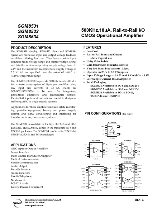
SGM8531 SGM8532 SGM8534PRODUCT DESCRIPTIONThe SGM8531 (single),SGM8532 (dual) and SGM8534 (quad) are rail-to-rail input and output voltage feedback amplifiers offering low cost. They have a wide input common-mode voltage range and output voltage swing, and take the minimum operating supply voltage down to 2.1V and the maximum recommended supply voltage is 5.5 V. All are specified over the extended –40°C to +125°C temperature range.The SGM8531/8532/8534 provide 500KHz bandwidth at a low current consumption of 18µA per amplifier. Very low input bias currents of 0.5pA, enable the SGM8531/8532/8534 to be used for integrators, photodiode amplifiers, and piezoelectric sensors. Rail-to-Rail inputs and outputs are useful to designers buffering ASIC in single-supply systems.Applications for these amplifiers include safety monitor- ing, portable equipment, battery and power supply control, and signal conditioning and interfacing for transducers in very low power systems.The SGM8531 is available in the tiny SOT23-5 and SO-8 packages. The SGM8532 comes in the miniature SO-8 and MSOP-8 packages. The SGM8534 is offered in TSSOP-14, TSSOP-16, SO-14 and SO-16 packages.APPLICATIONSASIC Input or Output Amplifier Sensor InterfacePiezo Electric Transducer Amplifier Medical Instrumentation Mobile Communication Audio Output Portable Systems Smoke Detectors Mobile Telephone Notebook PC PCMCIA cardsBattery-Powered equipment500KHz,18µA, Rail-to-Rail I/O CMOS Operational AmplifierFEATURES• Low Cost• Rail-to-Rail Input and Output0.8mV Typical V OS • Unity Gain Stable• Gain Bandwidth Product: : 500KHz • Very low input bias currents : 0.5pA • Operates on 2.1 V to 5.5 V Supplies• Input Voltage Range = - 0.1 V to +5.6 V with V S = 5.5V • Low Supply Current: 18µA/Amplifier • Small PackagingSGM8531 Available in SO-8 and SOT23-5 SGM8532 Available in SO-8 and MSOP-8 SGM8534 Available in SO-14, SO-16, TSSOP-14 and TSSOP-16PIN CONFIGURATIONS (Top View)S NC-V NC OUT S-V SOT23-5OUT B S -V SO-8 / MSOP-8OUT -IN A +IN A S +V -IN DD SO-16 / TSSOP-16-INB +IN B -IN C NCOUT BOUT C C D OUT +V -IN B +INB OUT BS -IN D+IN D -IN C OUT C+IN C OUT DShengbang Microelectronics Co, Ltd REV . CELECTRICAL CHARACTERISTICS : V S = +5V (At R L = 200kΩ connected to Vs/2 and V OUT = Vs/2, unless otherwise noted)Specifications subject to change without notice.PACKAGE/ORDERING INFORMATIONMODEL ORDER NUMBER PACKAGEDESCRIPTIONPACKAGE OPTION MARKING INFORMATIONSGM8531XN5/TRSOT23-5Tape and Reel, 30008531 SGM8531SGM8531XS/TR SO-8 Tape and Reel, 2500 SGM8531XS SGM8532XS/TR SO-8 Tape and Reel, 2500 SGM8532XS SGM8532SGM8532XMS/TRMSOP-8Tape and Reel, 3000SGM8532XMS SGM8534XS/TR SO-16 Tape and Reel, 2500SGM8534XSSGM8534XS14 SO-14Tube SGM8534XS14SGM8534XTS/TR TSSOP-16 Tape and Reel, 3000 SGM8534XTSSGM8534SGM8534XTS14 TSSOP-14TubeSGM8534XTS14ABSOLUTE MAXIMUM RATINGSSupply Voltage, V+ to V- ........................................... 7.5 VCommon-Mode Input Voltage.......................................... (–V S ) – 0.5 V to (+V S )+0.5VStorage Temperature Range.................. –65℃ to+150℃ Junction Temperature ................................................160℃ Operating Temperature Range ............ –55℃ to +150℃Package Thermal Resistance @ T A = 25℃SOT23-5, θJA .............................................................. 190/W ℃ SO-8, θJA ......................................................................125/W ℃ MSOP-8, θJA .............................................................. 216/W ℃ SO-16, θJA ..................................................................... 82/℃W TSSOP-16, θJA ............................................................ 105/W ℃ Lead Temperature Range (Soldering 10 sec).....................................................260℃ESD SusceptibilityHBM................................................................................4000V MM (400V)NOTES1. Stresses above those listed under Absolute Maximum Ratings may cause permanent damage to the device. This is a stress rating only; functional operation of the device at these or any other conditions above those indicated in the operational section of this specification is not implied. Exposure to absolute maximum rating conditions for extended periods may affect device reliability.CAUTIONThis integrated circuit can be damaged by ESD. Shengbang Micro-electronics recommends that all integrated circuits be handled with appropriate precautions. Failure to observe proper handling and installation procedures can cause damage.ESD damage can range from subtle performance degradation to complete device failure. Precision integrated circuits may be more susceptible to damage because very small parametric changes could cause the device not to meet its published specifications.TYPICAL PERFORMANCE CHARACTERISTICSAt T A = +25℃, V S = +5V , and R L =200k Ω connected to Vs/2,unless otherwise noted.Small-Signal Step Response Small-Signal Step Response10µs/div 10µs/divG = +1C L = 100pF R L = 5K ΩG = +1 C L = 100pF R L= 200K ΩG = +1 C L = 100pF R L= 200K Ω20m V /d i v50m V /d i v500m V /d i vLarge-Signal Step Response20µs/divTYPICAL PERFORMANCE CHARACTERISTICS At T A= +25℃, V S = +5V, and R L=200kΩ connected to Vs/2,unless otherwise noted.TYPICAL PERFORMANCE CHARACTERISTICSAt T A = +25℃, V S = +5V , and R L =200k Ω connected to Vs/2,unless otherwise noted.2.5V0V 250mV0VVs = 5V G = -10 V IN = 250mVTime(20μs/div)Overload Recovery TimeAPPLICATION NOTESDriving Capacitive LoadsThe SGM853X can directly drive 250pF in unity-gain without oscillation. The unity-gain follower (buffer) is the most sensitive configuration to capacitive loading. Direct capacitive loading reduces the phase margin of amplifiers and this results in ringing or even oscillation. Applications that require greater capacitive drive capability should use an isolation resistor between the output and the capacitive load like the circuit in Figure 1. The isolation resistor R ISO and the load capacitor C L form a zero to increase stability. The bigger the R ISO resistor value, the more stable V OUT will be. Note that this method results in a loss of gain accuracy because R ISO forms a voltage divider with the R LOAD.V IN V OUTFigure 1. Indirectly Driving Heavy Capacitive LoadAn improvement circuit is shown in Figure 2, It provides DC accuracy as well as AC stability. R F provides the DC accuracy by connecting the inverting signal with the output, C F and R Iso serve to counteract the loss of phase margin by feeding the high frequency component of the output signal back to the amplifier’s inverting input, thereby preserving phase margin in the overall feedback loop.V IN V OUTFigure 2. Indirectly Driving Heavy Capacitive Load with DC AccuracyFor no-buffer configuration, there are two others ways to increase the phase margin: (a) by increasing the amplifier’s gain or (b) by placing a capacitor in parallel with the feedback resistor to counteract the parasitic capacitance associated with inverting node. Power-Supply Bypassing and Layout The SGM853X family operates from either a single +2.5V to +5.5V supply or dual ±1.25V to ±2.75V supplies. For single-supply operation, bypass the power supply V DD with a 0.1µF ceramic capacitor which should be placed close to the V DD pin. For dual-supply operation, both the V DD and the V SS supplies should be bypassed to ground with separate 0.1µF ceramic capacitors. 2.2µF tantalum capacitor can be added for better performance.VnVpV SSV SS(GND)Figure 3. Amplifier with Bypass CapacitorsTypical Application Circuits Differential AmplifierThe circuit shown in Figure 4 performs the difference function. If the resistors ratios are equal ( R4 / R3 = R2 / R1 ), thenV OUT = ( Vp – Vn ) × R2 / R1 + Vref.Vn VpOUT Figure 4. Differential AmplifierInstrumentation AmplifierThe circuit in Figure 5 performs the same function as that in Figure 4 but with the high input impedance.Vn VpV OUT Figure 5. Instrumentation AmplifierLow Pass Active FilterThe low pass filter shown in Figure 6 has a DC gain of ( - R2 / R1 ) and the –3dB corner frequency is 1/2πR2C. Make sure the filter is within the bandwidth of the amplifier. The Large values of feedback resistors can couple with parasitic capacitance and cause undesired effects such as ringing or oscillation in high-speed amplifiers. Keep resistors value as low as possible and consistent with output loading consideration.V INV OUT Figure 6. Low Pass Active FilterPACKAGE OUTLINE DIMENSIONS SOT23-5PACKAGE OUTLINE DIMENSIONS SO-8PACKAGE OUTLINE DIMENSIONS MSOP-8PACKAGE OUTLINE DIMENSIONS SO-16PACKAGE OUTLINE DIMENSIONS TSSOP-16PACKAGE OUTLINE DIMENSIONS SO-14PACKAGE OUTLINE DIMENSIONS TSSOP-14REVISION HISTORYLocation Page 11/06— Data Sheet changed from REV.A to REV.BChanges to ABSOLUTE MAXIMUM ATINGS . . . . . . . . . . . . . . . . . . . . . . . . . . . . . . . .. . . . . . . . . . . . . . . . . . . . . . . . . . .. . . . . . . 3 05/07— Data Sheet changed from REV.B to REV.CAdds SO-14 and TSSOP-14 Package . . . . . . . . . . . . . . . . . . . . . . . . . . . . . . . . . . . . . . . . . . . . . . . .. . . . . . . . . . . . . . . . .. 1,3,14,15Shengbang Microelectronics Co, LtdUnit 3, ChuangYe PlazaNo.5, TaiHu Northern Street, YingBin Road Centralized Industrial ParkHarbin Development ZoneHarbin, HeiLongJiang 150078P.R. ChinaTel.: 86-451-84348461Fax: 86-451-84308461。
SGM321中文资料

MODEL SGM321 SGM358
SGM324
PACKAGE/ORDERING INFORMATION
ORDER NUMBER
SGM321YC5/TR SGM321YN5/TR SGM358YS/TR SGM358YMS/TR
SGM358YP SGM324YS/TR SGM324YTS/TR SGM324YS14/TR SGM324YTS14/TR
The SGM321 is available in SOT23-5 and SC70-5 packages. The SGM358 comes in SO-8,MSOP-8 and PDIP-8 packages. The SGM324 is offered in SO-14, TSSOP-14, TSSOP-16 and SO-16 packages.
11 -INC +INB 5 10 OUT C -INB 6
10 +INT
9 NC
OUT B 7
8 OUT C
TSSOP-16 / SO-16
TSSOP-14/SO-14
Shengbang Microelectronics Co, Ltd Tel: 86/451/84348461
The SGM321/358/324 provide 1MHz bandwidth at a low current consumption of 60µA per amplifier. Very low input bias currents of 10pA, enable SGM321/358/ 324 to be used for integrators, photodiode amplifiers, and piezoelectric sensors. Rail-to-rail inputs and outputs are useful to designers buffering ASIC in single-supply systems.
红芯半导体产品手册2014
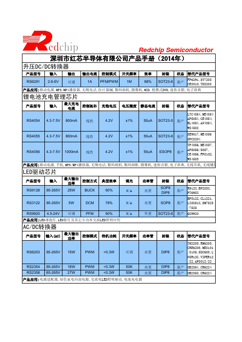
量产 OB2358,CR6224
产品应用:电源适配器,绿色家电内部电源,交流电LED照明驱动,电池充电器
Redchip Semiconductor 深圳市红芯半导体有限公司产品手册(2014年)
马达驱动芯片
产品型号 输入 驱动电流 静态电流 待机电流
热保护
RS117/118 1.8-7.2V 1.5A 300uA 0.1uA
±1%
50uA
ESOP8
量产
TP4056,ME4057, AP5056/5057, CE4056,FP8102, WS4503
产品应用:移动电源,手机,MP3/MP4播放器,无绳电话,数码相机,数码相框,摄像机,迷你音箱,电子辞典,无线耳机,无线键鼠
LED驱动芯片
产品型号
最大输出
输入
控制方式 典型效率
产品型号输入输出输出电流控制模式开关频率效率封装状态替代产品型号rs6291266v可调1apfmpwm1m88sot236量产fp6291sy7208ce8310td8208产品型号输入最大充电电流控制拓补充饱电压电压精度静态电流封装状态替代产品型号rs40544375v800ma线性42v150uasot235量产ltc4054me4054ap5054ce4054bl4054an4054ws4502rs40554375v800ma线性42v150uasot236量产se9017me4055spc8204rs40564375v1000ma线性42v150uaesop8量产tp4056me4057ap50565057ce4056fp8102ws4503产品型号输入最大输出功率控制方式典型效率调光功率管封装状态替代产品型号rs912885265v25wbuck90内置sop8dip8量产r912xbp283xpt698xrs312285265v5wdcm78内置sop8量产bp3122cl1221lis851xsm75237525rs99204524v可调pfm90外置sot236量产qx9920产品型号输入ac最大输出功率控制模式待机功耗开关频率功率管封装状态替代产品型号rs620385265v15wpwm03w可调内置dip8量产thx203rm6203cre6203me81018105sdc603ln5r12cviper1222ap801222rs235485265v16wpwm03w50k内置dip8量产ob2354cr6224rs235885265v27wpwm03w50k内置dip8量产ob2358cr6224redchipsemiconductor深圳市红芯半导体有限公司产品手册2014年升压dcdc转换器产品应用
SGM811中文资料
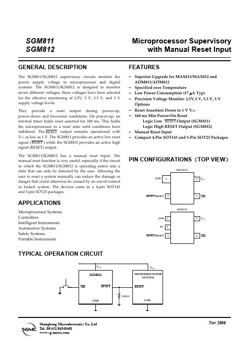
SGM811 SGM812Microprocessor Supervisorywith Manual Reset InputORDERING INFORMATIONORDERING NUMBERRESETTHRESHOLD(V)PECKAGETYPESPECIFIEDTEMPERATURERANGEPACKAGEMARKINGPACKAGEOPTIONSGM811-LXN5 4.63 SOT23-5 - 40°C to +125°C 811L Tape and Reel, 3000 SGM811-M XN5 4.38 SOT23-5 - 40°C to +125°C 811M Tape and Reel, 3000 SGM811-JXN5 4.00 SOT23-5 - 40°C to +125°C 811J Tape and Reel, 3000 SGM811-T XN5 3.08 SOT23-5 - 40°C to +125°C 811T Tape and Reel, 3000 SGM811-S XN5 2.93 SOT23-5 - 40°C to +125°C 811S Tape and Reel, 3000 SGM811-R XN5 2.63 SOT23-5 - 40°C to +125°C 811R Tape and Reel, 3000 SGM811-Z XN5 2.32 SOT23-5 - 40°C to +125°C 811Z Tape and Reel, 3000 SGM811-LXKA4 4.63 SOT143-4 - 40°C to +125°C 811L Tape and Reel, 3000 SGM811-MX KA4 4.38 SOT143-4 - 40°C to +125°C 811M Tape and Reel, 3000 SGM811-JX KA4 4.00 SOT143-4 - 40°C to +125°C 811J Tape and Reel, 3000 SGM811-TX KA4 3.08 SOT143-4 - 40°C to +125°C 811T Tape and Reel, 3000 SGM811-SX KA4 2.93 SOT143-4 - 40°C to +125°C 811S Tape and Reel, 3000 SGM811-RX KA4 2.63 SOT143-4 - 40°C to +125°C 811R Tape and Reel, 3000 SGM811-Z X KA4 2.32 SOT143-4 - 40°C to +125°C 811Z Tape and Reel, 3000 SGM812-LXN5 4.63 SOT23-5 - 40°C to +125°C 812L Tape and Reel, 3000 SGM812-M XN5 4.38 SOT23-5 - 40°C to +125°C 812M Tape and Reel, 3000 SGM812-JXN5 4.00 SOT23-5 - 40°C to +125°C 812J Tape and Reel, 3000 SGM812-T XN5 3.08 SOT23-5 - 40°C to +125°C 812T Tape and Reel, 3000 SGM812-S XN5 2.93 SOT23-5 - 40°C to +125°C 812S Tape and Reel, 3000 SGM812-R XN5 2.63 SOT23-5 - 40°C to +125°C 812R Tape and Reel, 3000 SGM812-Z XN5 2.32 SOT23-5 - 40°C to +125°C 812Z Tape and Reel, 3000 SGM812-LX KA4 4.63 SOT143-4 - 40°C to +125°C 812L Tape and Reel, 3000 SGM812-MX KA4 4.38 SOT143-4 - 40°C to +125°C 812M Tape and Reel, 3000 SGM812-JX KA4 4.00 SOT143-4 - 40°C to +125°C 812J Tape and Reel, 3000 SGM812-TX KA4 3.08 SOT143-4 - 40°C to +125°C 812T Tape and Reel, 3000 SGM812-SX KA4 2.93 SOT143-4 - 40°C to +125°C 812S Tape and Reel, 3000 SGM812-RX KA4 2.63 SOT143-4 - 40°C to +125°C 812R Tape and Reel, 3000 SGM812-Z X KA4 2.32 SOT143-4 - 40°C to +125°C 812Z Tape and Reel, 3000SGM811/8122ELECTRICAL CHARACTERISTICS(V CC Typ = 5 V for L/M/J Models, 3.3 V for T/S Models, 3 V for R Models, 2.5 V for Z Models; unless otherwise noted.)SGM811/8123SGM811/8124ELECTRICAL CHARACTERISTICS (continued)(V CC Typ = 5 V for L/M/J Models, 3.3 V for T/S Models, 3 V for R Models, 2.5 V for Z Models; unless otherwise noted.)Specifications subject to change without notice.ABSOLUTE MAXIMUM RATINGS(Typical values are at T A = 25°C, unless otherwise noted.) Terminal Voltage (With Respect to Ground)V CC ................................................................................–0.3 V to +6 V All Other Inputs ............................................ –0.3 V to V CC + 0.3 V Input CurrentVCC , ................................................................................ 20 mA Output CurrentRESET , RESET ..................................................................... 20 mA Power Dissipation, P D @ T A = 25℃SOT23-5 .....................................................................................0.4W SOT143-4.................................................................................. 0.32W Operating Temperature Range...........................- 40°C to +125°C Junction Temperature...........................................................+150°C Storage Temperature.............................................- 65°C to +150°C Lead Temperature (soldering, 10s).....................................+260°C ESD SusceptibilityHBM..........................................................................................4000V MM. (400V)Stresses beyond those listed under “Absolute Maximum Ratings” may cause permanent damage to the device. These are stress ratings only, and functional operation of the device at these or any other conditions beyond those indicated in the operational sections of the specifications is not implied. Exposure to absolute maximum rating conditions for extended periods may affect device reliability.PIN DESCRIPTIONTYPICAL PERFORMANCE CHARACTERISTICSTYPICAL PERFORMANCE CHARACTERISTICSAPPLICATION NOTESMANUAL RESETThe SGM811/SGM812 is equipped with a manual reset input This input is designed to operate in a noisy environment where unwanted glitches could be induced. These glitches could be produced by the bouncing action of a switch contact,or where a manual reset switch may be located some distance away from the circuit (the cabling of which may pick-up noise).The manual reset input is guaranteed to ignore logically valid inputs that are faster than 100 ns and to accept inputs longer in duration than 10 µs.BENEFITS OF A VERY ACCURATE RESET THRESHOLD Because the SGM811/SGM812 can operate effectively even when there are large degradations of the supply voltages, the possibility of a malfunction during a power failure is greatly reduced. Another advantage of the SGM811/SGM812 is its very accurate internal voltage reference circuit. Combined, these benefits produce an exceptionally reliable microprocessor supervisory circuit.Figure 1. Ensuring a Valid Output Down to V CC = 0VENSURING A VALID RESET OUTPUT DOWN TO V CC = 0 V When V CC falls below1.0 V, the SGM811/SGM812’s RESET no longer sinks current. Therefore, a high impedance CMOS logic input connected to RESET may drift to undetermined logic levels. To eliminate this problem, a 100 kΩ resistor should be connected from RESET to ground. RESET OUTPUTOn power-up and after V CC rises above the reset threshold, an internal timer holds the reset output active for 240 ms (typical). This is intended as a power-on reset signal for the processor. It allows time for both the power supply and the microprocessor to stabilize after power-up. If a power supply brownout or interruption occurs, the reset output is similarly activated and remains active for 240 ms (typical) after the supply recovers. This allows time for the power supply and microprocessor to stabilize.The SGM811 provides an active low reset output (RESET) while the SGM812 provides an active high output (). During power-down of the SGM811, the RESET output remains valid (low) with V CC as low as 1 V. This ensures that the microprocessor is held in a stable shutdown condition as the supply falls and also ensures that no spurious activity can occur via the microprocessor as it powers up.Glitch ImmunityThe SGM811/SGM812 contains internal filtering circuitry providing glitch immunity from fast transient glitches on the power supply line.RESETV CC1RESETV REF =RESET Voltage ThresholdFigure 2. Power Fail RESET TimingINTERFACING TO OTHER DEVICESOutputThe SGM811/SGM812 is designed to integrate with as many devices as possible. One feature of the SGM811/SGM812 is the reset output, which is directly proportional to V CC (this is guaranteed only while V CC is greater than 1 V). This enables the part to be used with both 3 V and 5 V, or any nominal voltage within the minimum and maximum specifications for V CC.PACKAGE OUTLINE DIMENSIONS SOT23-5PACKAGE OUTLINE DIMENSIONS SOT143- 4。
敏源传感科技有限公司单总线数字温度传感芯片产品手册(V3.5)说明书
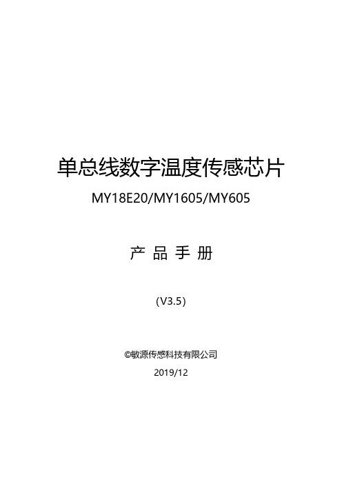
单总线数字温度传感芯片 MY18E20/MY1605/MY605产 品 手 册(V3.5)©敏源传感科技有限公司2019/12概述敏源传感数字温度传感芯片系列为高集成度的数字模拟混合信号的智能传感芯片,感温原理基于半导体PN节温度与带隙电压的特性关系,经过小信号放大、模数转换、数字校准补偿、输出数字温度,具有精度高、一致性好、寿命长、功耗低、可编程配置灵活等优点。
每颗芯片都有唯一的64位ID序列号,并在出厂前根据温度误差特性进行校准系数的拟合,芯片内部自动进行补偿计算。
为了简化系统应用,芯片的ID搜索、测温数据内存访问、功能配置等均基于数字单总线协议指令,上位机微处理器只需要一个GPIO端口便可进行读写访问。
单总线通信接口通过共用一根数据总线来实现了多节点传感采集与组网的低成本方案,传输距离远、支持节点数多,便于空间分布式传感组网。
芯片内置非易失性EEPROM存储单元,用于保存芯片ID号、高低温报警阈值、温度校准修正值以及用户自定义信息,如传感器节点编号、位置信息等。
温度传感芯片具有-55°C到+125°C的工业级工作范围,内置14-bit ADC,最高分辨率0.015°C;针对不同行业应用,产品分为0.1~1.0°C等不同精度等级。
MY18E20、MY1605、MY1820、MY605为标准版系列,最高测温精度为0.5°C 。
另有高精度可编程数字温度芯片MY605+、MY1605+ 、MY18E20+,可编程高精度0.1~0.3°C 。
根据不同应用需求,封装形式分为TO-92直插型MY18E20、TO-92S小尺寸直插型MY1820、SOT23-3表贴型MY1605、DFN-8表贴型MY605等不同规格。
特点-10°C~+85°C 0.5°C精度-55°C~+125°C 1.0°C精度单总线接口,适用于分布式多节点测温转换温度时间可配置:15ms/114ms/514ms标准版默认12位输出,分辨率0.0625°C【另有高精度系列为14位可编程输出,最高分辨率0.015°C】宽供电电压范围1.8V-5.5V 每颗芯片有可编程的ID 序列号,便于组网寻址 用户可自行设置报警值80-bit 存储空间用于存放用户信息 典型待机功耗0.2µA@5V ,最大测温峰值功耗0.3mA@5V 应用简单,无需额外器件典型应用工业监控、智能家电、智能硬件、智慧农业、仪器仪表封装管脚描述及实物图TO-92直插型 MY18E20SOT 表贴型 MY1605(2.9mm×2.8mm)DFN 表贴型 MY605(2mm*2mm)TO-92S 小直插型MY1820【芯片内部系统构成以MY18E20为例,其他封装型号等同。
SGM2013-1.8中文资料

300mA,Low Power,Low Dropout, SGM2013 3-Terminal,Linear RegulatorsSG Microelectronics Co, LtdREV. C Tel: 86/451/84348461ORDERING INFORMATIONMODELV OUT (V)PIN- PACKAGESPECIFIED TEMPERATURERANGE ORDERING NUMBERPACKAGE MARKINGPACKAGE OPTIONSOT23-3 SGM2013-1.8XN3/TRXD18 Tape and Reel, 3000SOT89-3SGM2013-1.8XK3/TR SGM2013-1.8XK3Tape and Reel, 1000SGM2013-1.8 1.8VSOT89-3(L-Type)- 40°C to +125°CSGM2013-1.8XK3L/TRSGM2013-1.8XK3L Tape and Reel, 1000SOT23-3 SGM2013-2.5XN3/TR XD25 Tape and Reel, 3000SOT89-3SGM2013-2.5XK3/TR SGM2013-2.5XK3Tape and Reel, 1000SGM2013-2.5 2.5VSOT89-3(L-Type)- 40°C to +125°CSGM2013-2.5XK3L/TRSGM2013-2.5XK3L Tape and Reel, 1000SOT23-3 SGM2013-2. 7XN3/TR XD27 Tape and Reel, 3000SOT89-3SGM2013-2. 7XK3/TRSGM2013-2. 7XK3 Tape and Reel, 1000SGM2013-2.7 2. 7VSOT89-3(L-Type)- 40°C to +125°CSGM2013-2. 7XK3L/TR SGM2013-2. 7XK3L Tape and Reel, 1000SOT23-3 SGM2013-2.8XN3/TR XD28 Tape and Reel, 3000SOT89-3SGM2013-2.8XK3/TR SGM2013-2.8XK3Tape and Reel, 1000SGM2013-2.8 2.8VSOT89-3(L-Type)- 40°C to +125°CSGM2013-2.8XK3L/TRSGM2013-2.8XK3L Tape and Reel, 1000SOT23-3 SGM2013-2.9XN3/TR XD29 Tape and Reel, 3000SOT89-3SGM2013-2.9XK3/TR SGM2013-2.9XK3Tape and Reel, 1000SGM2013-2.9 2.9VSOT89-3(L-Type)- 40°C to +125°CSGM2013-2.9XK3L/TRSGM2013-2.9XK3L Tape and Reel, 1000SOT23-3 SGM2013-3.0XN3/TR XD30 Tape and Reel, 3000SOT89-3SGM2013-3.0XK3/TR SGM2013-3.0XK3Tape and Reel, 1000SGM2013-3.0 3.0VSOT89-3(L-Type)- 40°C to +125°CSGM2013-3.0XK3L/TRSGM2013-3.0XK3L Tape and Reel, 1000SOT23-3 SGM2013-3.3XN3/TR XD33 Tape and Reel, 3000SOT89-3SGM2013-3.3XK3/TR SGM2013-3.3XK3Tape and Reel, 1000SGM2013-3.3 3.3VSOT89-3(L-Type)- 40°C to +125°CSGM2013-3.3XK3L/TRSGM2013-3.3XK3L Tape and Reel, 1000ABSOLUTE MAXIMUM RATINGSIN to GND.....................................................................- 0.3V to +6VOutput Short-Circuit Duration............................................Infinite OUT to GND...................................................- 0.3V to (V IN + 0.3V) Power Dissipation, P D @ T A = 25℃SOT23-3 .....................................................................................0.4W SOT89-3 ................................................................................0.571W Package Thermal ResistanceSOT23-3, θJA ....................................................................... 250/W ℃SOT89-3, θJA .........................................................................175°C/W Operating Temperature Range................. ..........- 40°C to +125°C Junction Temperature...........................................................+150°C Storage Temperature.............................................- 65°C to +150°C Lead Temperature (soldering, 10s).......................................260°C ESD SusceptibilityHBM..........................................................................................4000V MM. (400V)Stresses beyond those listed under “Absolute Maximum Ratings” may cause permanent damage to the device. These are stress ratings only, and functional operation of the device at these or any other conditions beyond those indicated in the operational sections of the specifications is not implied. Exposure to absolute maximum rating conditions for extended periods may affect device reliability.PIN DESCRIPTIONNAME FUNCTIONINRegulator Input. Supply voltage can range from 2.5V to 5.5V. GND Ground.OUT Regulator Output.ELECTRICAL CHARACTERISTICS(V IN= V OUT(NOMINAL)+ 0.5V (1), T A= - 40°C to +125°C, unless otherwise noted. Typical values are at T A= + 25°C.)PARAMETER SYMBOL CONDITIONS MINTYPMAXUNITSInput Voltage V IN 2.55.5VOutput Voltage Accuracy(1)I OUT =1mA to 300mA, T A = +25°CV OUT + 0.5V≤V IN≤ 5.5V-3 +3 %Maximum Output Current 300 mA Current Limit I LIM310 750 mANo load, 77 145Ground Pin Current I QI OUT = 300mA, 200µAI OUT = 1mA 0.8Dropout Voltage (2)I OUT = 300mA 300 380mVLine Regulation(1)ΔV LNR V IN = 2.5V or (V OUT +0.5V) to 5.5V,I OUT = 1mA0.03 0.15 %/VLoad Regulation ΔV LDR I OUT = 0.1mA to 300mA, C OUT = 1µF 0.0008 0.002 %/mAf = 100Hz, 75 dB Power Supply Rejection Rate PSRR I LOAD = 50mA, C OUT = 1µFf = 1KHz, 53 dB THERMAL PROTECTIONThermal Shutdown Temperature T SHDN160 ℃Thermal Shutdown Hysteresis ΔT SHDN15 ℃Specifications subject to change without notice.Note 1:V IN = V OUT(NOMINAL) + 0.5V or 2.5V, whichever is greater.Note 2: The dropout voltage is defined as V IN - V OUT, when V OUT is 100mV below the value of V OUT for V IN = V OUT + 0.5V. (Only applicable forV OUT = +2.5V to +5.0V.)TYPICAL OPERATING CHARACTERISTICSV IN = V OUT (NOMINAL) + 0.5V or 2.5V (whichever is greater), C IN = 1µF, C OUT = 1µF, T A = +25℃, unless otherwise noted.TYPICAL OPERATING CHARACTERISTICSV IN = V OUT (NOMINAL) + 0.5V or 2.5V (whichever is greater), C IN = 1µF, C OUT = 1µF, T A = +25℃, unless otherwise noted.TYPICAL OPERATING CHARACTERISTICSV IN = V OUT (NOMINAL) + 0.5V or 2.5V (whichever is greater), C IN = 1µF, C OUT = 1µF, T A = +25℃, unless otherwise noted.Application NotesWhen LDO is used in handheld products, Attention must be paid to voltage spike which would damage SGM2013. In such applications, voltage spike will be generated at changer interface and V BUS pin of USB interface when changer adapters and USB equipments are hot-inserted. Besides this, handheld products will be tested on the production line on the condition of no battery. Test Engineer will apply power from the connector pin which connects with positive pole of the battery. When external power supply is turned on suddenly, the voltage spike will be generated at the battery connector. The voltage spike will be very high, it always exceeds the absolute maximum input voltage (6.0V) of LDO. In order to get robust design. Design Engineer needs to clear up this voltage spike. Zener diode is a cheap and effective solution to eliminate such voltage spike. For example, BZM55B5V6 is a 5.6V small package Zener diode which can be used to remove voltage spike in cell phone design. The schematic is shown in below:PACKAGE OUTLINE DIMENSIONS SOT23-3PACKAGE OUTLINE DIMENSIONS SOT89-3REVISION HISTORYLocation Page12/06— Data Sheet changed from REV. A to REV. BChanged to ABSOLUTE MAXIMUM RATINGS . . . . . . . . . . . . . . . . . . . . . . . . . . . . . . . . . . . . . . . . . . . . . . . . . . . . . . . . . . . . . . . . . . . . . . . . 2 Added Application Notes . . . . . . . . . . . . . . . . . . . . . . . . . . . . . . . . . . . . . . . . . . . . . . . . . . . . . . . . . . . . . . . . . . . . . . . . . . . . . . . . . . . . . . . . . . . .7 03/07— Data Sheet changed from REV. B to REV. CChanged to TYPICAL OPERATING CHARACTERISTICS . . . . . . . . . . . . . . . . . . . . . . . . . . . . . . . . . . . . . . . . . . . . . . . . . . . . . . . . . . . . . . . 5Shengbang Microelectronics Co, LtdUnit 3, ChuangYe PlazaNo.5, TaiHu Northern Street, YingBin Road Centralized Industrial ParkHarbin Development Zone150078HeiLongJiangHarbin,ChinaP.R.Tel.: 86-451-84348461Fax: 86-451-84308461。
sgm321用法
sgm321用法全文共四篇示例,供读者参考第一篇示例:SGM321是一种高性能、低功耗的精密电压参考源。
它广泛应用于各种电子设备中,特别是需要高精度参考电压的电路中。
在本文中,我们将重点介绍SGM321的用法及其在电子设计中的重要性。
SGM321通常被用作模拟电路中的参考电压源。
在许多模拟电路中,需要一个稳定的参考电压来确保整个电路的稳定性和精度。
SGM321可以提供高精度、低漂移的参考电压,从而确保整个电路在各种工作条件下都能保持稳定。
除了作为参考电压源外,SGM321还可以作为电源管理电路中的关键部件。
在许多电源管理电路中,需要对电压进行监控和调整以确保系统的稳定性和效率。
SGM321可以帮助实现这一功能,其高精度和低功耗的特性使其成为电源管理电路中不可或缺的部件。
SGM321还可以用于传感器和仪器等精密测量设备中。
在这些应用中,需要一个高精度、稳定的参考电压源来确保测量结果的准确性。
SGM321的高性能特性可以满足这些应用的需求,从而提高测量的精度和可靠性。
第二篇示例:SGM321是一种高性能、低电压运算放大器,具有低噪声、高增益、宽带宽和低电压漂移等特点。
它通常用于精密仪器、传感器信号处理、滤波器设计等领域。
本文将介绍SGM321的主要特性、用法和注意事项。
在实际应用中,SGM321的用途非常广泛。
首先是在精密仪器中的应用,如医疗设备、实验仪器等,可以用来放大微弱信号进行测量和控制。
其次是在传感器信号处理中的应用,如温度传感器、压力传感器等,可以提高信噪比和动态范围。
SGM321还可以用于滤波器设计,在音频处理、信号处理等领域有着广泛的应用。
在使用SGM321时,需要注意一些事项。
首先是供电电压,SGM321通常工作在低电压范围内,建议选择适当的稳压电源以确保其正常工作。
其次是引脚的连接,正确连接输入、输出和电源引脚以避免引起焊接错误或损坏芯片。
还要注意信号的输入范围和匹配性,选择合适的外部元件以满足电路设计要求。
MPS6531中文资料
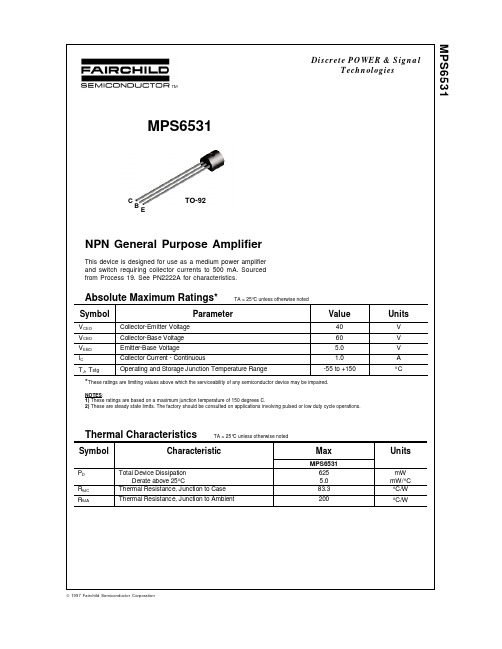
Max
MPS6531 625 5°C/W
© 1997 Fairchild Semiconductor Corporation
元器件交易网
MPS6531
NPN General Purpose Amplifier
(continued)
Electrical Characteristics
Symbol Parameter
TA = 25°C unless otherwise noted
Test Conditions
Min
Max
Units
OFF CHARACTERISTICS
V(BR)CEO V(BR)CBO V(BR)EBO ICBO Collector-Emitter Breakdown Voltage* Collector-Base Breakdown Voltage Emitter-Base Breakdown Voltage Collector Cutoff Current I C = 10 mA, I B = 0 I C = 10 µA, I E = 0 I E = 10 µA, IC = 0 VCB = 40 V, IE = 0 VCB = 40 V, IE = 0, TA = 60 °C 40 60 5.0 50 2.0 V V V nA µA
Absolute Maximum Ratings*
Symbol
VCEO VCBO VEBO IC TJ, Tstg Collector-Emitter Voltage Collector-Base Voltage Emitter-Base Voltage Collector Current - Continuous
NOTES: 1) These ratings are based on a maximum junction temperature of 150 degrees C. 2) These are steady state limits. The factory should be consulted on applications involving pulsed or low duty cycle operations.
SGM8631-2-3-4低噪声运算放大器
SG Micro Corp
2
SGM8631/2/3/4
470μA, 6MHz, Rail-to-Rail I/O CMOS Operational Amplifiers
PACKAGE OPTION Tape and Reel, 3000 Tape and Reel, 3000 Tape and Reel, 2500 Tape and Reel, 3000 Tape and Reel, 2500 Tape and Reel, 3000 Tape and Reel, 2500 Tape and Reel, 2500 Tape and Reel, 3000
APPLICATIONS
Sensors Audio Active Filters A/D Converters Communications Test Equipment Cellular and Cordless Phones Laptops and PDAs Photodiode Amplification Battery-Powered Instrumentation
智邦控股
Mr zhang 13828730731
SGM8Rail-to-Rail I/O CMOS Operational Amplifiers
PRODUCT DESCRIPTION
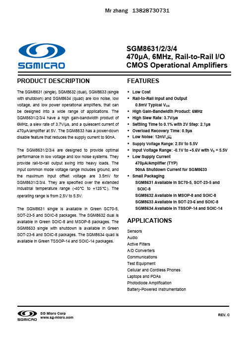
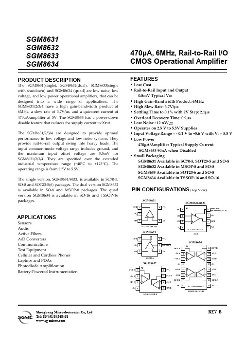
The SGM8631 (single), SGM8632 (dual), SGM8633 (single with shutdown) and SGM8634 (quad) are low noise, low voltage, and low power operational amplifiers, that can be designed into a wide range of applications. The SGM8631/2/3/4 have a high gain-bandwidth product of 6MHz, a slew rate of 3.7V/μs, and a quiescent current of 470μA/amplifier at 5V. The SGM8633 has a power-down disable feature that reduces the supply current to 90nA. The SGM8631/2/3/4 are designed to provide optimal performance in low voltage and low noise systems. They provide rail-to-rail output swing into heavy loads. The input common mode voltage range includes ground, and the maximum input offset voltage are 3.5mV for SGM8631/2/3/4. They are specified over the extended industrial temperature range (-40 ℃ to +125 ℃ ). The operating range is from 2.5V to 5.5V. The SGM8631 single is available in Green SC70-5, SOT-23-5 and SOIC-8 packages. The SGM8632 dual is available in Green SOIC-8 and MSOP-8 packages. The SGM8633 single with shutdown is available in Green SOT-23-6 and SOIC-8 packages. The SGM8634 quad is available in Green TSSOP-14 and SOIC-14 packages.
AD8631中文资料
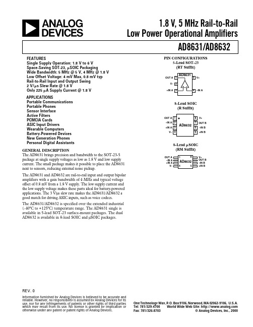
Large Signal Voltage Gain
OUTPUT CHARACTERISTICS Output Voltage Swing High
0 V ≤ VCM ≤ 5 V, –40؇C ≤ TA ≤ +125؇C RL = 10 kΩ, 0.5 V < VOUT < 4.5 V RL = 100 kΩ, 0.5 V < VOUT < 4.5 V RL = 100 kΩ, –40؇C ≤ TA ≤ +125؇C
IL = 100 µA –40؇C ≤ TA ≤ +125؇C IL = 1 mA IL = 100 µA –40؇C ≤ TA ≤ +125؇C IL = 1 mA Short to Ground, Instantaneous
VOS IB IOS VCM CMRR
AVO
Offset Voltage Drift Bias Current Drift
OUTPUT CHARACTERISTICS Output Voltage Swing High
∆VOS/∆T ∆IB/∆T
VOH
Output Voltage Swing Low
ELECTRICAL CHARACTERISTICS (VS = 2.2 V, V– = 0 V, VCM = 1.1 V, TA = 25؇C unless otherwise noted)
Parameter
Symbol
Conditions
Min Typ Max
SGM8634中文资料
CONDITION
TYP +25℃ +25℃
0.8
3.5
1
1
VS = 5.5V
-0.1 to +5.6
VS = 5.5V, VCM = - 0.1V to 4 V
90
75
VS = 5.5V, VCM = - 0.1V to 5.6 V
83
RL = 600Ω ,Vo = 0.15V to 4.85V
97
SO-8 MSOP-8
SO-8 SOT23-6
SO-8 SO-16 TSSOP-16
PACKAGE OPTION Tape and Reel, 3000 Tape and Reel, 3000 Tape and Reel, 2500 Tape and Reel, 3000 Tape and Reel, 2500 Tape and Reel, 3000 Tape and Reel, 2500 Tape and Reel, 2500 Tape and Reel, 3000
OUT A 1 -IN A 2 +IN A 3 -VS 4
8 +VS
+INB 5
7 OUT B -INB 6
OUT B 7 6 -IN B
5 +IN B
NC 8
SO-8 / MSOP-8
NC = NO CONNECT SO-8
SGM8634
NC = NO CONNECT TSSOP-16 / SO-16
NC 1 -IN 2
8
DISABLE (SGM8633 ONLY)
7 +VS
+IN 3
6 OUT
SOT23-5 / SC70-5
SGM4056中文资料

2
PPR
3 4 5 6
CHG EN GND IMIN
7
IREF
8
BAT
典型应用电路
பைடு நூலகம்图 1.带指示 LED
图 2.带指示信号和 MCU 接口
图 1 的组件描述 器件 C1 C2 RIREF RIMIN R1,R2 D1,D2 描述 1uF X5R 陶瓷电阻 1uF X5R 陶瓷电阻 24.3KΩ,1%(500mA 充电电流) 243KΩ,1%(40mA 充电截止电流) 300Ω,5% 指示 LED 灯 器件 C1 C2 RIREF RIMIN R1,R2
图 2 的组件描述 描述 1uF X5R 陶瓷电阻 1uF X5R 陶瓷电阻 24.3KΩ,1%(500mA 充电电流) 243KΩ,1%(40mA 充电截止电流) 100KΩ,5%
SGM4056
圣邦微电子
高输入电压的充电管理芯片
引脚排列
引脚定义
引脚 1 名称 VIN 功能
电源输入脚。最大输入电压是 26.5V。 此处接一个 1uF 或更大的 X5R 陶瓷 去耦电容,建议将电容放置在离引脚非常近的位置。可能需要接额外的 电容以稳定输入电压。 开漏电源存在指示脚。 当输入电压高于 POR 阈值低于 OVP 阈值时开漏 MOS 管打开。此管脚以最小 15mA 的电流驱动一个 LED,最大电压为 5.5V,并独 立于 EN 管脚输入。 开漏充电指示脚。当充电循环开始时为低电平,当充电结束时输出为高 电平, 此管脚以最小 15mA 的电流驱动一个 LED,当充电芯片被禁用时,此 管脚输出高阻抗。 使能脚。是一个用来禁用或启动充电管理芯片的逻辑输入口,置高时禁 用充电芯片, 此脚置低或浮空时, 启用充电芯片, 此管脚内部有一个 200K Ω的下拉电阻。 系统地。 充电截止电流编程编程脚。在此脚和 GND 之间接一个电阻设置 EOC 电流, 充电截止电流 IMIN 可通过下面的公式计算I = − 0.5(mA),RMIN 单 位为 KΩ。可编程范围为充电电流的 5%(或 10mA,以较高者为准)-50%。 当设定为小于 5%充电电流或 10mA 时,无法保证稳定性。 充电电流编程监测脚。在此脚与 GND 之间连接电阻用以设置极限充电电 流,充电电流由以下公式得出:I = − 4(mA),RIREF 单位是 KΩ。 编程电阻应非常靠近此管脚,此管脚电压用以监测整个充电周期内的实 际充电电流,包括涓流、恒流和恒压阶段。当禁用时,VIREF=0V。 充电输出脚。连接电池正极,此处接一个 1uF 或更大的陶瓷电容用于去 耦和稳定充电电流。当 EN 端被拉到逻辑高时,BAT 输出被禁用。
SGM9111中文资料

PACKAGE DESCRIPTION
SO-8 SO-8
TEMPERATURE RANGE
-40℃ to +85℃ 0℃ to +70℃
PACKAGE OPTION Tape and Reel, 2500 Tape and Reel, 2500
MARKING INFORMATION
CAUTION
This integrated circuit can be damaged by ESD. Shengbang Micro-electronics recommends that all integrated circuits be handled with appropriate precautions. Failure to observe proper handling and installation procedures can cause damage. ESD damage can range from subtle performance degradation to complete device failure. Precision integrated circuits may be more susceptible to damage because very small parametric changes could cause the device not to meet its published specifications.
Video amplifiers Cable and Satellite set top boxes Communications devices Video on demand Portable and handheld products Personal video recorders DVD players HDTV
mt8631微功耗霍尔开关的工作原理及应用

mt8631微功耗霍尔开关的工作原理及应用MT8631微功耗霍尔开关是一种新型的无源电子设备,通过霍尔效应实现非接触式开关功能,具有低功耗、高灵敏度、寿命长等特点。
下面将详细介绍MT8631微功耗霍尔开关的工作原理及应用。
一、工作原理MT8631微功耗霍尔开关的工作原理基于霍尔效应。
霍尔效应是指放置在磁场中的导电材料中,当其两侧施加一定电势差时,会在材料的一侧产生电流,这个电流与施加的电势差和磁场强度成正比。
MT8631微功耗霍尔开关内部集成了霍尔传感器、信号处理电路和开关输出电路。
当磁场作用在霍尔传感器上时,传感器产生霍尔电压(Hall Voltage),信号处理电路通过对霍尔电压的采集和处理,可以判断磁场的强弱和方向。
根据信号处理电路的设计,当磁场超过设定阈值时,开关输出电路打开或关闭,实现开关的控制功能。
二、特点1.低功耗:MT8631微功耗霍尔开关采用CMOS工艺设计,工作电压低,静态工作电流仅为几微安,因此功耗非常低,适用于要求长时间稳定工作的电池供电设备。
2.高灵敏度:MT8631微功耗霍尔开关具有极高的灵敏度,对磁场的探测距离较远,可以达到几毫米或更远的距离。
3.无触点:MT8631微功耗霍尔开关采用无触点的工作原理,不需要使用机械接触器,因此具有寿命长、维护方便等优点。
4.高可靠性:MT8631微功耗霍尔开关的内部电路采用集成化设计,具有较高的抗干扰能力和稳定性,可在各种复杂环境中正常工作。
三、应用1.电动工具:将MT8631微功耗霍尔开关应用于电动工具中,可实现电动机的控制和保护功能。
例如,当电动工具的握柄离开用户时,磁场变化会被霍尔开关探测到,可以实现电动工具的自动停止。
2.智能家居:MT8631微功耗霍尔开关可用于智能家居中的门磁开关、窗磁开关等场景。
当门窗关闭时,霍尔开关处于闭合状态,当门窗打开时,霍尔开关断开,通过检测霍尔开关的状态可以实现门窗的开关状态检测。
3.安防系统:MT8631微功耗霍尔开关还可以应用于安防系统中。
英飞凌 PMG1-S2 第一代供电微控制器 数据表

请注意赛普拉斯已正式并入英飞凌科技公司。
此封面页之后的文件标注有“赛普拉斯”的文件即该产品为此公司最初开发的。
请注意作为英飞凌产品组合的部分,英飞凌将继续为新的及现有客户提供该产品。
文件内容的连续性事实是英飞凌提供如下产品作为英飞凌产品组合的部分不会带来对于此文件的任何变更。
未来的变更将在恰当的时候发生,且任何变更将在历史页面记录。
订购零件编号的连续性英飞凌继续支持现有零件编号的使用。
下单时请继续使用数据表中的订购零件编号。
PMG1-S2数据手册第一代供电微控制器PMG1系列概述PMG1 (第一代供电微控制器) 是一系列的高电压 USB-C 供电 (PD) 微控制器 (MCU)。
这些芯片拥有一个Arm ® Cortex ®-M0/M0+CPU 、USB-C PD 控制器以及模拟和数字外设。
PMG1适用于向/从高电压USB-C PD 端口提供/消耗电源并利用微控制器提供额外控制功能的任何嵌入式系统。
图1说明了PMG1系列的细分。
图1.PMG1系列细分*更多有关PMG1-S2的信息,请联系您所在地的带普拉斯销售办事处。
表1显示了PMG1系列中不同MCU 的性能对比。
*更多有关PMG1-S2的信息,请联系您所在地的带普拉斯销售办事处。
文档的其余部分详细介绍了有关PMG1-S2器件的内容。
表1. PMG1系列中不同MCU 的性能对比子系统或范围条目PMG1-S0PMG1-S1PMG1-S2PMG1-S3*CPU 和存储器子系统内核 ARM Cortex-M0ARM Cortex-M0ARM Cortex-M0Arm Cortex-M0+最大频率 (MHz)48484848Flash (KB)64 128128256SRAM (KB)812832供电供电端口11148-QFN 具有一个端口97-BGA 具有两个端口功能灌电流DRP DRP DRP MOSFETx 栅极驱动器1x PFET 2x PFET2x NFET 灵活的2x NFET 故障保护VBUS OVP 和UVPVBUS OVP , UVP 和OCP SCP 和RCP (仅适用于发送源配置)。
- 1、下载文档前请自行甄别文档内容的完整性,平台不提供额外的编辑、内容补充、找答案等附加服务。
- 2、"仅部分预览"的文档,不可在线预览部分如存在完整性等问题,可反馈申请退款(可完整预览的文档不适用该条件!)。
- 3、如文档侵犯您的权益,请联系客服反馈,我们会尽快为您处理(人工客服工作时间:9:00-18:30)。
SGM8631 SGM8632 SGM8633 SGM8634470µA, 6MHz, Rail-to-Rail I/O CMOS Operational AmplifierShengbang Microelectronics Co, Ltd REV . BELECTRICAL CHARACTERISTICS :V S = +5V (At T A = +25℃,V CM = Vs/2,R L = 600Ω, unless otherwise noted)Specifications subject to change without notice.PACKAGE/ORDERING INFORMATIONMODEL ORDERNUMBER PACKAGEDESCRIPTION PACKAGEOPTIONMARKINGINFORMATIONSGM8631XC5/TR SC70-5 Tape and Reel, 3000 8631SGM8631XN5/TR SOT23-5 Tape and Reel, 3000 8631 SGM8631SGM8631XS/TR SO-8 Tape and Reel, 2500SGM8631XSSGM8632XMS/TR MSOP-8 Tape and Reel, 3000 SGM8632XMS SGM8632SGM8632XS/TR SO-8 Tape and Reel, 2500 SGM8632XSSGM8633XN6/TR SOT23-6 Tape and Reel, 3000 8633 SGM8633SGM8633XS/TR SO-8 Tape and Reel, 2500 SGM8633XSSGM8634XS/TR SO-16 Tape and Reel, 2500 SGM8634XS SGM8634SGM8634XTS TSSOP-16 Tape and Reel, 3000 SGM8634XTSABSOLUTE MAXIMUM RATINGS Supply Voltage, V+ to V- ............................................ 7.5 V Common-Mode Input Voltage.................................... (–V S) – 0.5 V to (+V S) +0.5V Storage Temperature Range..................... –65℃ to +150℃Junction Temperature.................................................160℃Operating Temperature Range.................–55℃ to +150℃Package Thermal Resistance @ T A = 25℃SC70-5, θJA................................................................ 333/W℃SOT23-5, θJA.............................................................. 190/W℃SOT23-6, θJA.............................................................. 190/W℃SO-8, θJA......................................................................125/W℃MSOP-8, θJA.............................................................. 216/W℃SO-16, θJA..................................................................... 82/W℃TSSOP-16, θJA............................................................ 105/W℃Lead Temperature Range (Soldering 10 sec).....................................................260℃ESD Susceptibility HBM.. (1500V)MM (400V)NOTES1. Stresses above those listed under Absolute Maximum Ratings may cause permanent damage to the device. This is a stress rating only; functional operation of the device at these or any other conditions above those indicated in the operational section of this specification is not implied. Exposure to absolute maximum rating conditions for extended periods may affect device reliability. CAUTIONThis integrated circuit can be damaged by ESD. Shengbang Micro-electronics recommends that all integrated circuits be handled with appropriate precautions. Failure to observe proper handling and installation procedures can cause damage.ESD damage can range from subtle performance degradation to complete device failure. Precision integrated circuits may be more susceptible to damage because very small parametric changes could cause the device not to meet its published specifications.TYPICAL PERFORMANCE CHARACTERISTICSAt T A = +25℃,V CM = Vs/2, R L = 600Ω, unless otherwise noted.Positive Overload Recovery Negative Overload RecoveryTime(2µs/div) Time(500ns/div)Large-Signal Step Response Small-Signal Step ResponseTime(1µs/div) Time(1µs/div)0V 0VVs = ±2.5V V IN = 50mV R L = 10K Ω G = 1002.5V -50mV 0V 0V2.5V-50mVVs = ±2.5V V IN = 50mV R L = 10K Ω G = 100Vs = 5VG = +1 C L = 100pF R L = 10K ΩVs = 5V G = +1 C L = 100pF R L = 10K ΩV o l t a g e (1V /d i v )V o l t a g e (50m V /d i v )TYPICAL PERFORMANCE CHARACTERISTICS At T A = +25℃,V CM = Vs/2, R L = 600Ω, unless otherwise noted.TYPICAL PERFORMANCE CHARACTERISTICS At T A = +25℃,V CM = Vs/2, R L = 600Ω, unless otherwise noted.TYPICAL PERFORMANCE CHARACTERISTICSAt T A = +25℃,V CM = Vs/2, R L = 600Ω, unless otherwise noted.Large-Signal Step Response Small-Signal Step ResponseTime(1µs/div) Time(1µs/div)Vs=2.7VG=+1C L=100pFR L=10KΩVs=2.7VG=+1C L=100pFR L=10KΩVoltage(5mV/div)Voltage(5mV/div)TYPICAL PERFORMANCE CHARACTERISTICS At T A = +25℃,V CM = Vs/2, R L = 600Ω, unless otherwise noted.APPLICATION NOTESDriving Capacitive LoadsThe SGM863x can directly drive 1000pF in unity-gain without oscillation. The unity-gain follower (buffer) is the most sensitive configuration to capacitive loading. Direct capacitive loading reduces the phase margin of amplifiers and this results in ringing or even oscillation. Applications that require greater capacitive drive capability should use an isolation resistor between the output and the capacitive load like the circuit in Figure 1. The isolation resistor R ISO and the load capacitor C L form a zero to increase stability. The bigger the R ISO resistor value, the more stable V OUT will be. Note that this method results in a loss of gain accuracy because R ISO forms a voltage divider with the R LOAD.V IN V OUTFigure 1. Indirectly Driving Heavy Capacitive LoadAn improvement circuit is shown in Figure 2. It provides DC accuracy as well as AC stability. R F provides the DC accuracy by connecting the inverting signal with the output. C F and R Iso serve to counteract the loss of phase margin by feeding the high frequency component of the output signal back to the amplifier’s inverting input, thereby preserving phase margin in the overall feedback loop.V IN V OUTFigure 2. Indirectly Driving Heavy Capacitive Load with DC AccuracyFor no-buffer configuration, there are two others ways to increase the phase margin: (a) by increasing the amplifier’s gain or (b) by placing a capacitor in parallel with the feedback resistor to counteract the parasitic capacitance associated with inverting node. Power-Supply Bypassing and Layout The SGM863x family operates from either a single +2.5V to +5.5V supply or dual ±1.25V to ±2.75V supplies. For single-supply operation, bypass the power supply V DD with a 0.1µF ceramic capacitor which should be placed close to the V DD pin. For dual-supply operation, both the V DD and the V SS supplies should be bypassed to ground with separate 0.1µF ceramic capacitors. 2.2µF tantalum capacitor can be added for better performance.Good PC board layout techniques optimize performance by decreasing the amount of stray capacitance at the op amp’s inputs and output. To decrease stray capacitance, minimize trace lengths and widths by placing external components as close to the device as possible. Use surface-mount components whenever possible.For the operational amplifier, soldering the part to the board directly is strongly recommended. Try to keep the high frequency big current loop area small to minimize the EMI (electromagnetic interfacing).VnVpV SSVnV SS(GND)Figure 3. Amplifier with Bypass Capacitors GroundingA ground plane layer is important for SGM863x circuit design. The length of the current path speed currents in an inductive ground return will create an unwanted voltage noise. Broad ground plane areas will reduce the parasitic inductance.Input-to-Output CouplingTo minimize capacitive coupling, the input and output signal traces should not be parallel. This helps reduce unwanted positive feedback.Typical Application CircuitsDifferential AmplifierThe circuit shown in Figure 4 performs the difference function. If the resistors ratios are equal ( R4 / R3 = R2 / R1 ), then V OUT = ( Vp – Vn ) × R 2 / R 1 + Vref.Vn VpOUTFigure 4. Differential AmplifierInstrumentation AmplifierThe circuit in Figure 5 performs the same function as that in Figure 4 but with the high input impedance.VnVpV OUTFigure 5. Instrumentation AmplifierLow Pass Active FilterThe low pass filter shown in Figure 6 has a DC gain of (-R 2/R 1) and the –3dB corner frequency is 1/2πR 2C. Make sure the filter is within the bandwidth of the amplifier. The Large values of feedback resistors can couple with parasitic capacitance and cause undesired effects such as ringing or oscillation inhigh-speed amplifiers. Keep resistors value as low as possible and consistent with output loading consideration.V INV OUTFigure 6. Low Pass Active FilterSC70-5SOT23-5SOT23-6SO-8MSOP-8SO-16TSSOP-16REVISION HISTORYLocation Page 11/06— Data Sheet changed from REV.A to REV.BAdded SC70-5 PACKAGE . . . . . . . . . . . . . . . . . . . . . . . . . . . . . . . . . . . . . . . . . . . . . . . . . . . . . . . . . . . . . . .. . . . . . . Universal Changes to PRODUCT DESCRIPTION, FEATURES, and PIN CONFIGURATIONS . . . . . . . . . . .. . . . . . . . . . . . .. . 1 Updated PACKAGE/ORDERING INFORMATION. . . . . . . . . . . . . . . . . . . . . . . . . . . . . . . . . . . . . . . . . .. . . . . . . . . . . . . .. .3 Changes to ABSOLUTE MAXIMUM ATINGS . . . . . . . . . . . . . . . . . . . . . . . . . . . . . . . .. . . . . . . . . . . . . . . . . . . . . . . . . . .. . . . . . . 3Shengbang Microelectronics Co, LtdUnit 3, ChuangYe PlazaNo.5, TaiHu Northern Street, YingBin Road Centralized Industrial ParkHarbin Development Zone150078HeiLongJiangHarbin,ChinaP.R.Tel.: 86-451-84348461Fax: 86-451-84308461。
