P4001中文资料
EP1C12Q240C8N中文资料(Altera)中文数据手册「EasyDatasheet - 矽搜」

注意 表 1-1: (1) 该参数包括全局时钟引脚.
EP1C3 59,904
1 104
EP1C4 78,336
2 301
EP1C6 92,160
2 185
EP1C12 239,616
2 249
Cyclone器件在四方扁平封装(QFP),并提供节省空间
FineLine ® BGA封装(见
表1-2
通过 1–3).
于接口和支持ASSP和ASIC器件. Altera还提供新低成本串行配置设备
配置Cyclone器件.
特征
Cyclone器件系列具有以下特性:
■ 2,910 20060个LE,见
表1-1
■ 高达294,912 RAM位(36,864字节)
■ 通过低成本串行配置设备支持配置
■ 支持LVTTL,LVCMOS,SSTL-2和SSTL-3 I / O标准
65
EP1C4
—
EP1C6
—
EP1C12
—
EP1C20
—
104
—
—
—
—
—
—
—
249
301
98
185
185
—
—
—
173
185
249
—
—
—
—
233
301
须知 表 1-2: (1) TQFP:薄型四方扁平封装.
PQFP:塑料四方扁平封装. (2) Cyclone器件支持在同一封装内垂直迁移(即,设计人员可以之间迁移
BGA
1.0
441
21×21
文件 修订记录
表1-4
显示修订历史此文档.
表 1-4.文档修订历史记录
PA01资料
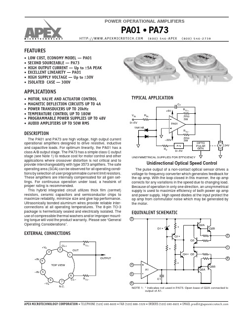
POWER SUPPLY
VOLTAGE CURRENT, quiescent
THERMAL
Full temperature range TC = 25°C
RESISTANCE, AC, junction to case4 RESISTANCE, DC, junction to case RESISTANCE, junction to air TEMPERATURE RANGE, case
元器件交易网
MICROTECHNOLOGY
POWER OPERATIONAL AMPLIFIERS
PA01 • PA73
(800) 546-APEX (800) 546-2739
FEATURES
• LOW COST, ECONOMY MODEL — PA01 • SECOND SOURCEABLE — PA73 • HIGH OUTPUT CURRENT — Up to ±5A PEAK • EXCELLENT LINEARITY — PA01 • HIGH SUPPLY VOLTAGE — Up to ±30V • ISOLATED CASE — 300V
PHASE MARGIN
Full temperature range
OUTPUT
VOLTAGE SWING3 VOLTAGE SWING3 VOLTAGE SWING3 CURRENT, peak SETTLING TIME to .1% SLEW RATE CAPACITIVE LOAD, unity gain CAPACITIVE LOAD, gain > 4
TC = 25°C, VCM = VS –6V
OPEN LOOP GAIN at 10Hz
REF01中文手册

REF01数据表1、元器件参数特性1)High output accuracy(高输出精度)REF01: 10.0 V, ±0.3% maximumREF02: 5.0 V, ±0.3% maximumREF03: 2.5 V, ±0.6% maximum2)Excellent temperature stability(良好的温度稳定特性)REF01: 8.5 ppm/°C maximumREF02: 8.5 ppm/°C maximumREF03: 50 ppm/°C maximum3)Low noise(低噪声)REF01: 30 µV p-p typicalREF02: 15 µV p-p typicalREF03: 6 µV p-p typical最高供电电压范围:最大达36 V最低供电电流:最大值为1.4 mA高负荷驱动能力:最大10 mA(最大输出负载电流)温度输出功能(温度监控)应用场景精密数据系统高分辨率转换器工业过程控制系统精密仪器军事和航空航天应用概述REF01/REF02/REF03系列精密电压参考产品提供了稳定的10.0 V、5.0 V或2.5 V输出,且随供应电压、环境温度或负载条件的变化影响最小。
该设备有8引脚的SOIC、PDIP、CERDIP 和TO-99封装,以及20端口的LCC封装(仅883),进一步提高了该设备在标准和高压力应用中的可用性。
通过一个外部缓冲器和一个简单的电阻网络,TEMP终端可以用于温度传感和近似。
在该装置上还提供了一个TRIM端子,用于微调输出电压。
REF01、REF02/REF03系列应用非常适合通用和空间受限的应用。
较新的设计应使用ADR01/ADR02/ADR03/ADR06系列参考文献,可提供更高的精度和温度。
1、引脚配置不同封装下的引脚图如下:注:NC = NO CONNECT ,即不要在这些引脚上连接任何东西。
AO3401A中文资料
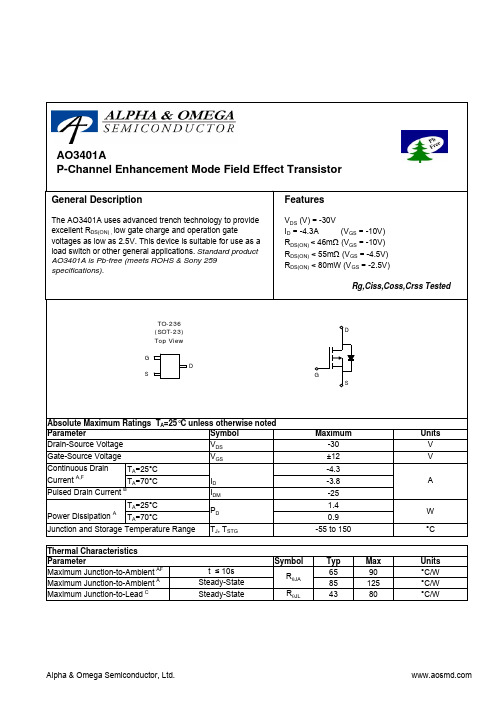
SymbolTyp Max 659085125R θJL 4380Maximum Junction-to-Lead CSteady-State°C/WThermal Characteristics ParameterUnits Maximum Junction-to-Ambient AF t ≤ 10s R θJA °C/W Maximum Junction-to-Ambient A Steady-State °C/W AO3401AAO3401ASymbolMin TypMaxUnits BV DSS -30V -1T J =55°C-5I GSS ±100nA V GS(th)-0.6-1-1.3V I D(ON)-25A 3644T J =125°C52634455m Ω6280m Ωg FS 13S V SD -0.75-1V I S-2A C iss 9331200pF C oss 108pF C rss 81pF R g69ΩQ g 9.312.2nC Q gs 1.5nC Q gd 3.7nC t D(on) 5.2ns t r 6.8ns t D(off)42ns t f 15ns t rr 2128ns Q rr14.3nCTHIS PRODUCT HAS BEEN DESIGNED AND QUALIFIED FOR THE CONSUMER MARKET. APPLICATIONS OR USES AS CRITICAL COMPONENTS IN LIFE SUPPORT DEVICES OR SYSTEMS ARE NOT AUTHORIZED. AOS DOES NOT ASSUME ANY LIABILITY ARISING OUT OF SUCH APPLICATIONS OR USES OF ITS PRODUCTS. AOS RESERVES THE RIGHT TO IMPROVE PRODUCT DESIGN,FUNCTIONS AND RELIABILITY WITHOUT NOTICE.Body Diode Reverse Recovery TimeBody Diode Reverse Recovery Charge I F =-4.3A, dI/dt=100A/µsDrain-Source Breakdown Voltage On state drain currentI D =-250µA, V GS =0V V GS =-2.5V, I D =-2.5AV GS =-4.5V, V DS =-5V V GS =-10V, I D =-4.3AReverse Transfer Capacitance Electrical Characteristics (T J =25°C unless otherwise noted)STATIC PARAMETERS ParameterConditions I DSS µA Gate Threshold Voltage V DS =V GS I D =-250µA V DS =-30V, V GS =0VV DS =0V, V GS =±12V Zero Gate Voltage Drain Current Gate-Body leakage current R DS(ON)Static Drain-Source On-ResistanceForward TransconductanceDiode Forward Voltage m ΩV GS =-4.5V, I D =-3.5A I S =-1A,V GS =0V V DS =-5V, I D =-4.3AI F =-4.3A, dI/dt=100A/µsV GS =0V, V DS =-15V, f=1MHz SWITCHING PARAMETERS Total Gate Charge V GS =-4.5V, V DS =-15V, I D =-4.3AGate Source Charge Gate Drain Charge Turn-On Rise Time Turn-Off DelayTime V GS =-10V, V DS =-15V, R L =3.5Ω, R GEN =6ΩGate resistanceV GS =0V, V DS =0V, f=1MHzTurn-Off Fall TimeMaximum Body-Diode Continuous CurrentInput Capacitance Output Capacitance Turn-On DelayTime DYNAMIC PARAMETERS A: The value of R θJA is measured with the device mounted on 1in 2 FR-4 board with 2oz. Copper, in a still air environment with T A =25°C. The value in any given application depends on the user's specific board design. B: Repetitive rating, pulse width limited by junction temperature.C. The R θJA is the sum of the thermal impedence from junction to lead R θJL and lead to ambient.D. The static characteristics in Figures 1 to 6 are obtained using <300 µs pulses, duty cycle 0.5% max.E. These tests are performed with the device mounted on 1 in 2 FR-4 board with 2oz. Copper, in a still air environment with T A =25°C. The SOA curve provides a single pulse rating.F.The current rating is based on the t ≤ 10s thermal resistance rating.Rev0: Apr.2007AO3401AAO3401A。
40PC015V2A中文资料

40PC015V2A中文资料Order Product and Get SupportU.S. Authorized DistributorsGlobal Sales & Service N. American Sales Reps Distributor Inventory Technical Assistance White P apers Literature Request Test and Measurement CatalogRoHS P roduct List Customer FeedbackHome> Products > Piezoresistive Silicon > 40PC > P roduct P age40PC015V2APressure Sensors: MeasurementType: Vacuum; Amplified; Range: 0 psito -15.0 psiActual product appearance may vary.Featuresl Smallest amplified sensor packagel Minimal P CB spacel Fully signal conditionedl Operating temperature range from -45 °C to 125 °C [-49 °F to 257 °F]l Silicon piezoresistive technologyl Monolithic designl 6 P in DIP packagel Port designed for O-ring interfacePotential ApplicationsMedicall Oxygen and nitrogen gas distribution inhospitalsl Dental chairsl CPAP (Continuous P ositive Airw ay Pressure) equipmentl Respirators and ventilatorsl Blood glucose monitorsl Oxygen conserversl Oxygen concentratorsl Nebulizersl Kidney dialysis machinesl Blood cell separatorsl Hospital bedsEnvironmentall Water control valvesl Instrumentationl Irrigation equipmentl Filter monitoring equipment Industrial Instrumentationl Roboticsl Pressure valvesl Leak detectionl Air compressorsAnalytical Instrumentationl Gas chromatographyl Chemical Analyzers Transportationl Electronic brake systemsl Engine oil levell Transmission fluid levell Air conditioning systeml Fuel injection systems DescriptionThe cost-effective 40PC Series miniature pressure sensor is the smallest amplifiedpressure sensor manufactured by Honeyw ell. The fully calibrated and temperature-compensated sensor is very robust, covering a w ide range of temperatureextremes. Additionally, the 40PC Series is compatible w ith a broad array of media,from dry air and w ater to refrigerant coolants and engine fuel. The 0.5 Vdc to 4.5Vdc analog output voltage signal is linearly proportional to input pressure. Thesedevices operate on a single end supply voltage of 5.0 Vdc.Supporting DocumentationNone AvailableProduct SpecificationsMeasurem ent Type Vacuum GageSignal Conditioning Am plifiedPressure Range0 psi to -15.0 psiMaxim um Overpressure30.0 psiSup ply Voltage 5.0 Vdc ±0.25 VdcCom pensated YesOutput Calibration YesResponse Tim e 1 m s m ax.Term ination PCB; Leads form ed away from portPort Style Straight for O-ring interfacePackage Style Honeywell - MonolithicLinearity0.30% span m ax.Typical Sensitivity266.6 m V/psiFull Scale Span 4.0 Vdc typ.Null Offset0.50 Vdc typ.Null Shift over Tem perature±2.00 m ax.Span Shift Over Tem perature±3.50 m ax.Repeatability & Hysteresis Error±0.15 % span typ.Shock Qualification tested to 150 gVibration MIL-STD-202 Method 213 (150 ghalf sine 11 m s)Operating Tem perature Range-45 °C to 125 °C [-49 °F to 257 °F]Com pensated Tem perature Range-45 °C to 85 °C [-49 °F to 185 °F]Storage Tem perature Range-55 °C to 125 °C [-67 °F to 257 °F]Media Com patibility Port 1: Dry gases only. Mediam ust be com patible with epoxy-based adhesive. Port 2: Wettedm aterials. Media m ust becom patible with glass, silicon,stainless steel, invar, Sn/Ni platingand Sn/Ag solder.UNSPSC Code411121UNSPSC Com m odity411121 TransducersAvailability GlobalSeries Nam e40PCMy LinksLogin to iCOMLogin as Rep/ADLogin as GuestLogin to DigitalUniversityKeyw ord SearchSearch for product andsupport information.All Sensing and ControlProduct SearchPart number search:Use (*) to expand searchSpecification SearchTerms & Conditions | Privacy Statement | Site Map 元器件交易网/doc/2316046389.html,。
各国硬质合金牌号对照表
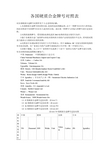
各国硬质合金牌号对照表对各国硬质合金牌号对照作发下5点说明和注解:1.各国硬质合金牌号的对照关系,是按用途范围确定的。
由于一种牌号往往有几种用途,因此对照表中有的牌号往往在几处同时出现,或出现一种牌号与其他几种牌号进行近似对照。
2.对照的基准牌号,采用国际标准化组织ISO标准的用途分类代号为序。
3.鉴于各硬质合金厂家的样本和技术资料所介绍的产品使用范围并不完全,所列的对照表只能表示大致的对比使用范围。
4.对照表中各国标准代号均用于大写字母表示,其中BHMAt JIC分别为英国和美国的有关协会标准。
各厂家或公司的产品牌号或商标用小写字母(第一字母仍大写)。
5.因限于篇幅,从上百个厂家资料中仅选择了十余个厂家和公司的产品牌号进行对照,有关对照的商标或简称注解如下:中国Diamond:中国机械进出口总公司China National Machinery Import and Export Corp.法国Carbex :Carbex SATykram:Tykram SAUgicarbb:Enrotungstene SA德国Hertel:GH-Metall,Gunther Hertel GmbH&Co.KGUnit:Thyssen Edelstahlwerke AGWidia:Rride.Krupp GmbH,Krupp Widia -Fabrik日本Igetalloy :住友电气工业(株)Sumitomo Electric Industries Ltd.瑞典Sandvik Coromant;Sandvik ABSeco:Seco Tools AB英国Annolly:F.C.Annett&Co.Led.Cutanit:Herbrt-Cutanit Ltd.Wimet :Wimet Ltd.美国Kennametal:Kennametal Inc.Wendt-Sonis:TRW,Wendt-Souis Div.(1)P类硬质合金牌号近似对照(表6-6-7)(2)M类硬质合金牌号近似对照(表6-6-8)(3)K类硬质合金牌号近似对照(表6-6-79)(4)G类硬质合金牌号近似对照(表6-6-10)表6-6-7 P类硬质合金牌号近似对照国际标准化组织IS O 中国德国法国日本YB Diamond DIN Widia UnitTykramCarbex JIS IgetalloyP01 YT30 T30 —TTF UF03 TS0 CSO P01 AC805 T12AP10 YT15 T15 S1 TGTNTRTTXUS10USS2BTS1CS10CS120RW211P10AC805AC815ST10ET12AP20 YT14 T14 S2 TGTNTRTTSUS20US52BTS2TSYCS20CS120RW211P20AC720AC815ST20ET3SP30 YT5 T5 S3 TGTNTTRTTSUS30US54BTS3TSYCS30CS120CS130RW211P30AC720AC835ST30ET3SP40 YT5 T5 S4 TRTTRUS40US54BTS4 CS4 P40AC835ST40EP50 ——S5 —US50 CS6 P50 —国际标准化组织IS O 俄罗斯ΓOCT瑞典英国美国SandvikCoromantSecoBHMAWimet Cutanit JICWendt-SonisKennametalP01 T30K4 F02S1PS1FS1G919 —CR05F05TC8731CY31TTi8K165K7HP10 T15K6 GC015GC1025S1PS1FS1GS2,S25MTP15TP25TP35722GW52XL2XL2BCR10CR15CR20CR30Gm25C7714CY14U227K5HK45KC810P20 T14K8 GC015GC135GC1025S4,SMS2,S4S25MTP15TP25444GW52XL3CR10CR15CR20CR25C6714716CY14CY16K29K2884KC810KC850SM30 TP35 CR30Gm25 U225 U227P30 T5K10 GC015GC1025S2,SMSM30S4,S6S25MTP15TP35353CW54XL45CR20CR25CR30CR40Gm35C5716717CY16U225K21K2884KC810KC850P40 TFK12RGC135S6SM30S6S25MTP35263CW54XL45CR30CR40CR50Gm35C5717CY17CY17TK25KC85CP50 T5K12BR4 182 CR50717CY17KM注:表中ISO标准为用途分类代号。
华为 P40 手机用户指南说明书
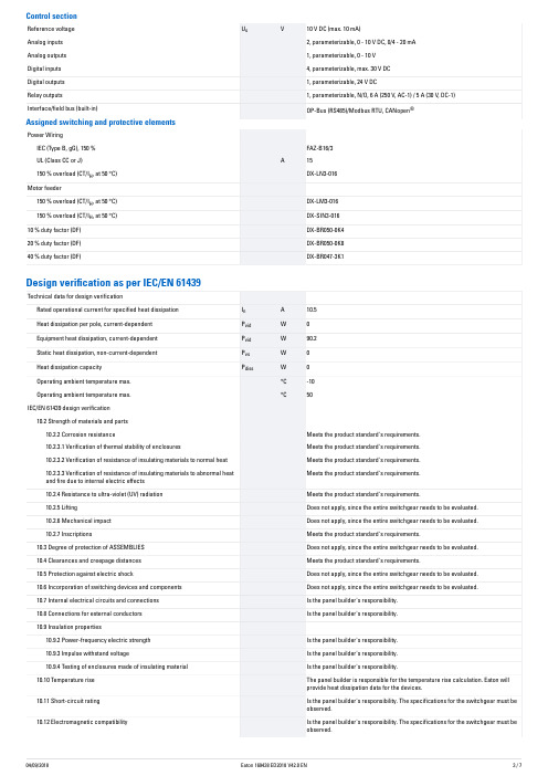
kW
2.2
With control unit
Yes
Application in industrial area permitted
Yes
Application in domestic- and commercial area permitted
Yes
Supporting protocol for TCP/IP
10.9 Insulation properties
10.9.2 Power-frequency electric strength
10.9.3 Impulse withstand voltage
10.9.4 Testing of enclosures made of insulating material
Mains voltage
V
200 - 240
Mains frequency
50/60 Hz
Number of phases input
3
Number of phases output
3
Max. output frequency
Hz
500
Rated output voltage
V
230
Measuring output current
Is the panel builder's responsibility. Is the panel builder's responsibility. Is the panel builder's responsibility. The panel builder is responsible for the temperature rise calculation. Eaton will provide heat dissipation data for the devices. Is the panel builder's responsibility. The specifications for the switchgear must be observed. Is the panel builder's responsibility. The specifications for the switchgear must be observed.
NF2401中文手册.doc
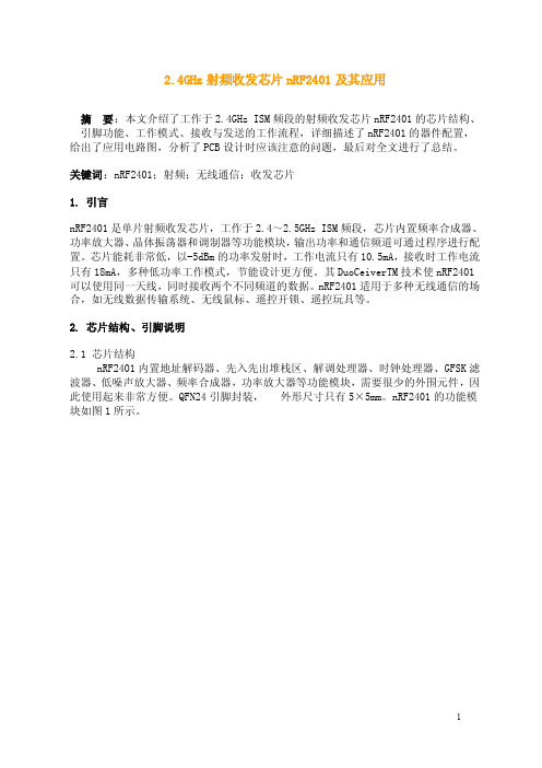
2.4GHz射频收发芯片nRF2401及其应用摘要:本文介绍了工作于2.4GHz ISM频段的射频收发芯片nRF2401的芯片结构、引脚功能、工作模式、接收与发送的工作流程,详细描述了nRF2401的器件配置,给出了应用电路图,分析了PCB设计时应该注意的问题,最后对全文进行了总结。
关键词:nRF2401;射频;无线通信;收发芯片1. 引言nRF2401是单片射频收发芯片,工作于2.4~2.5GHz ISM频段,芯片内置频率合成器、功率放大器、晶体振荡器和调制器等功能模块,输出功率和通信频道可通过程序进行配置。
芯片能耗非常低,以-5dBm的功率发射时,工作电流只有10.5mA,接收时工作电流只有18mA,多种低功率工作模式,节能设计更方便。
其DuoCeiverTM技术使nRF2401可以使用同一天线,同时接收两个不同频道的数据。
nRF2401适用于多种无线通信的场合,如无线数据传输系统、无线鼠标、遥控开锁、遥控玩具等。
2. 芯片结构、引脚说明2.1 芯片结构nRF2401内置地址解码器、先入先出堆栈区、解调处理器、时钟处理器、GFSK滤波器、低噪声放大器、频率合成器,功率放大器等功能模块,需要很少的外围元件,因此使用起来非常方便。
QFN24引脚封装,外形尺寸只有5×5mm。
nRF2401的功能模块如图1所示。
图2nRF2401引脚图2.2 引脚说明表1:nRF2401引脚(附:此处引脚11和12有误。
2006.6.30)3. 工作模式nRF2401有工作模式有四种:收发模式、配置模式、空闲模式和关机模式。
nRF2401的工作模式由PWR_UP 、CE、TX_EN和CS三个引脚决定,详见表2。
表2:nRF2401工作模式3.1 收发模式nRF2401的收发模式有ShockBurstTM收发模式和直接收发模式两种,收发模式由器件配置字决定,具体配置将在器件配置部分详细介绍。
3.1.1 ShockBurstTM收发模式ShockBurstTM收发模式下,使用片内的先入先出堆栈区,数据低速从微控制器送入,但高速(1Mbps)发射,这样可以尽量节能,因此,使用低速的微控制器也能得到很高的射频数据发射速率。
PR01中文资料

PR01中文资料Document Number: 28729For technical questions contact: ff3dresistors@/doc/05a24c1b52d380eb62 946dd4.html/doc/05a24c1b52d380eb62946dd4.ht mlPR01/02/03Vishay BCcomponentsPower Metal Film ResistorsFEATURESHigh power in small packagesDifferent lead materials for different applications ? Defined interruption behaviour.APPLICATIONSAll general purpose power applicationsA homogeneous film of metal alloy is deposited on a high grade ceramic body. After a helical groove has been cut in the resistive layer, tinned connecting wires of electrolytic copper or copper-clad iron are welded to the end-caps. The resistors are coated with a red, nonflammable lacquer which provides electrical, mechanical and climatic protection. This coating is not resistant to aggressive fluxes. The encapsulation is resistant to all cleaning solvents in accordance wi th “MIL-STD-202E, method 215”, and“IEC 60068-2-45”.Notes1. 1 % tolerance is available for R n -range from 1R upwards.2. 2 % tolerance is available on request for Rn -range from 1R upwards.3.Ohmic values (other than resistance range) are available on request.元器件交易网/doc/05a24c1b52d380eb62946dd4.htmlPR01/02/03Vishay BCcomponents Power Metal Film ResistorsNotes1.PR01 pitch 12.5 mm.2.PR02 pitch 15.0 mm.3.PR03 pitch 20.0 mm, with reversed kinking direction as opposed to the drawing for the type with double kink figure. ORDERING INFORMATIONOrdering Code (12NC)The resistors have a 12-digit ordering code starting with 23. For 5 % tolerance:The first 9 digits indicate the resistor type and packaging.?The remaining 3 digits indicate the resistance value: –The first 2 digits indicate the resistance value.–The last digit indicates the resistance decade.For 1% tolerance:The first 8 digits indicate the resistor type and packaging.?The remaining 4 digits indicate the resistance value: –The first 3 digits indicate the resistance value.–The last digit indicates the resistance /doc/05a24c1b52d380eb62946dd4.htmlst Digit of 12NC Indicating Resistance DecadeOrdering ExampleThe ordering code for resistor type PR02 with Cu leads and a value of 750 ? with 5 % tolerance, supplied on a bandolier of 1000 units in ammopack, is: 2306 198 53751.RESISTANCE DECADE LAST DIGIT0.22 to 0.91 ?71 to 9.76 ?810 to 97.6 ?9100 to 976 ?11 to 9.76 k?210 to 97.6 k?3100 to 976 k?41 M?5元器件交易网/doc/05a24c1b52d380eb62946dd4.html 元器件交易网/doc/05a24c1b52d380eb62946dd4.htmlPower Metal Film Resistors Vishay BCcomponentsDIMENSIONSType with straight leads.Type with double kink.Dimensions in millimeters.Document Number: 28729For technical questions contact: ff3dresistors@/doc/05a24c1b52d380eb62 946dd4.html/doc/05a24c1b52d380eb62946dd4.html PR01/02/03Vishay BCcomponentsPower Metal Film ResistorsMARKINGThe nominal resistance and tolerance are marked on the resistor using four coloured bands in accordance with IEC publication 60062, “Colour codes for fixed resistors”.OUTLINESThe length of the body (L 1) is measured by inserting the leads into holes of two identical gauge plates and moving these plates parallel to each other until the resistor body is clamped without deformation (“IEC publication 60294”).MOUNTINGThe resistors are suitable for processing on automatic insertion equipment and cutting and bending machines.Note1.Recommended minimum value.FUNCTIONAL DESCRIPTION PRODUCT CHARACTERIZATION Standard values of nominal resistance are taken from the E96/E24 series for resistors with a tolerance of ± 1 % or ± 5 %. The values of the E96/E24 s eries are in accordance with “IEC publication 60063”.FUNCTIONAL PERFORMANCEPR01 Drift nomogram.PR02 Drift nomogram.Note1.The maximum voltage that may be continuously applied to theresistor element, see “IEC publication 60115-1”.The maximum permissible hot-spot temperature is 205 °C for PR01,220 °C for PR02 and 250 °C for PR03.PR03 Drift nomogram.Document Number: 28729For technical questions contact: ff3dresistors@/doc/05a24c1b52d380eb62 946dd4.html/doc/05a24c1b52d380eb62946dd4.ht mlPR01/02/03Power Metal Film ResistorsVishay BCcomponentsThe power that the resistor can disipate depends on the operating temperature.DeratingMaximum dissipation (P max ) in percentage of rated power as a function of the ambient temperature (T amb ).PR01i ).max Pulse Loading CapabilitiesPR01 Pulse on a regular basis; maximum permissible peakpulse voltage as a function of pulse duration (t i ).V max ()PR01/02/03Vishay BCcomponentsPower Metal Film ResistorsPR02i ).max PR02i ).max Pulse Loading CapabilitiesPR03i ).maxDocument Number: 28729For technical questions contact: ff3dresistors@/doc/05a24c1b52d380eb62 946dd4.html/doc/05a24c1b52d380eb62946dd4.ht mlPR01/02/03Power Metal Film ResistorsVishay BCcomponentsPulse Loading CapabilitiesPR03 Pulse on a regular basis; maximum permissible peak pulse voltage as a function of pulse duration (t i ).V max ()PR01 Time to interruption as a function of overload powerfor range: 0 R 22 ≤ R n< 1 R.This graph is based on measured data under constant voltage conditions; the data may deviate according to the applications.power for range: 1 R ≤ R n≤ 15 R.This graph is based on measured data under constant voltage conditions; the data may deviate according to the applications.Interruption Characteristicspower for range: 16 R ≤ R n≤ 560 R.This graph is based on measured data under constant voltage conditions; the data may deviate according to the applications.power for range: 0.33 R ≤ R n < 5 R.This graph is based on measured data under constant voltage conditions; the data may deviate according to the applications.PR01/02/03Vishay BCcomponentsPower Metal Film ResistorsInterruption CharacteristicsPR02 Time to interruption as a function of overloadpower for range: 5 R ≤ R n < 68 R.This graph is based onmeasured data under constant voltage conditions; the data may deviate according to the applications.PR02 Time to interruption as a function of overloadpower for range: 68 R ≤ R n ≤ 560 R.This graph is based on measured data under constant voltage conditions; the data may deviate according to the applications.Interruption CharacteristicsPR03 Time to interruption as a function of overload power for range: 0.68 R≤ R n ≤ 560 R.This graph is based on measured data under constant voltage conditions; the data may deviate according to the applications.PR01 Hot-spot temperature rise (?T) as afunction of dissipated power.0.6 mm Cu-leads.Application InformationPR01 Temperature rise (?T) at the lead end (soldering point) as a function of dissipated power at various lead lengths after mounting.0.6 mm Cu-leads.Minimum distance from resistor body to PCB = 1 mm.PR01 Hot-spot temperature rise (?T) as a functionof dissipated power.Document Number: 28729For technical questions contact: ff3dresistors@/doc/05a24c1b52d380eb62 946dd4.html/doc/05a24c1b52d380eb62946dd4.ht mlPR01/02/03Power Metal Film ResistorsVishay BCcomponentsPR01 Temperature rise (?T) at the lead end (soldering point) as a function of dissipated power at various lead lengths after mounting.Minimum distance from resistor body to PCB = 1 mm.PR02 Hot-spot temperature rise (?T) as a function ofdissipated power.PR02 Temperature rise (?T) at the lead end (soldering point) as a function of dissipated power at various lead lengths after mounting.Minimum distance from resistor body to PCB = 1 mm.PR02Hot-spot temperature rise (?T) as a function ofdissipated power.Application InformationPR02 Temperature rise (?T) at the lead end (soldering point) as a function of dissipated power at various lead lengths after mounting.Minimum distance from resistor body to PCB = 1 mm.PR02 Hot-spot temperature rise (?T) as a functionof dissipated power.PR01/02/03Vishay BCcomponentsPower Metal Film ResistorsPR02 Temperature rise (?T) at the lead end (soldering point) as a function of dissipated power at various lead lengths after mounting.0.8 mm FeCu-leads.Minimum distance from resistor body to PCB = 1 mm.PR03 Hot-spot temperature rise (?T) as a function ofdissipated power.PR03 Temperature rise (?T) at the lead end (soldering point) as a function of dissipated power at various lead lengths after mounting.0.8 mm Cu-leads.Minimum distance from resistor body to PCB = 1 mm.PR03 Hot-spot temperature rise (?T) as a function ofdissipated power.Application InformationPR03 Temperature rise (?T) at the lead end (soldering point) as a function of dissipated power at various lead lengths after mounting.Minimum distance from resistor body to PCB = 1 mm.PR03 Hot-spot temperature rise (?T) as a function ofdissipated power.0.8 mm FeCu-leads.PR01/02/03Power Metal Film ResistorsVishay BCcomponentsDocument Number: 28729For technical questions contact: ff3dresistors@/doc/05a24c1b52d380eb62 946dd4.html/doc/05a24c1b52d380eb62946dd4.ht mlPR03 Temperature rise (?T) at the lead end (soldering point) as a function of dissipated power at various lead lengths after mounting.0.8 mm FeCu-leads.Minimum distance from resistor body to PCB = 1 mm.Application InformationPR01 Phase angle as a function of applied frequency./doc/05a24c1b52d380eb62946dd4.ht mlFor technical questions contact: ff3dresistors@/doc/05a24c1b52d380eb62 946dd4.htmlDocument Number: 28729PR01/02/03Vishay BCcomponentsPower Metal Film ResistorsPR02Impedance as a function of applied frequency.Application InformationPR03 Impedance as a function of applied frequency.Document Number: 28729For technical questions contact: ff3dresistors@/doc/05a24c1b52d380eb62 946dd4.html/doc/05a24c1b52d380eb62946dd4.ht mlPR01/02/03Power Metal Film ResistorsVishay BCcomponentsApplication InformationPR03 Phase angle as a function of applied frequency.TESTS AND REQUIREMENTSEssentially all tests are carried out in accordance with theschedule of “IEC publication 60115-1”, category LCT/UCT/56 (rated temperature range: Lower Category Temperature, Upper Category Temperature; damp heat,long term, 56 days). The testing also covers the requirements specified byEIA and EIAJ.The tests are carried out in accordance with IEC publication 60068-2, “Recommended basic climatic and mechanical robustness testing procedure for electronic components”and under standard atmospheric conditions according to “IEC 60068-1”, subclause 5.3.In the Test Procedures and Requirements table, tests and requirements are listed with reference to the relevant clauses of “IEC publications 60115-1 and 60068-2”; a short description of the test procedure is also given. In some instances deviations from the IEC recommendations were necessary for our method of specifying.All soldering tests are performed with mildly activated flux.PR01/02/03Vishay BCcomponents Power Metal Film Resistors/doc/05a24c1b52d380eb62946dd4.ht ml For technical questions contact: ff3dresistors@/doc/05a24c1b52d380eb62 946dd4.html Document Number: 28729。
USCAR中文第版
3.需要的参考文件。。。。。。。。。。。。。。。。。。。。。。。。。。。。。。。。。。。。。。。。。。。。。。。。。。。。。。。。。。5
3.1 文件的层次 。。。。。。。。。。。。。。。。。。。。。。。。。。。。。。。。。。。。。。。。。。。。。。。。。。。。。。。。5
5.6.5浸泡。。。。。。。。。。。。。。。。。。。。。。。。。。。。。。。。。。。。。。。。。。。。。。。。。。。。。。。。。。。。。。59
5.6.6压力/真空泄漏。。。。。。。。。。。。。。。。。。。。。。。。。。。。。。。。。。。。。。。。。。。。。。。。。。。。。61
5.7特殊试验。。。。。。。。。。。。。。。。。。。。。。。。。。。。。。。。。。。。。。。。。。。。。。。。。。。。。。。。。。63
5.4.9模腔损坏系数。。。。。。。。。。。。。。。。。。。。。。。。。。。。。。。。。。。。。。。。。。。。。。。。。。。。。。48
5.4.10端子/型腔极化测试。。。。。。。。。。。。。。。。。。。。。。。。。。。。。。。。。。。。。。。。。。。。。。。。54
5.5连接器电性能试验。。。。。。。。。。。。。。。。。。。。。。。。。。。。。。。。。。。。。。。。。。。。。。。。。。49
4.2 样品文献。。。。。。。。。。。。。。。。。。。。。。。。。。。。。。。。。。。。。。。。。。。。。。。。。。。。。。。。。。。7
4.3 样品数量。。。。。。。。。。。。。。。。。。。。。。。。。。。。。。。。。。。。。。。。。。。。。。。。。。。。。。。。。。。7
- 1、下载文档前请自行甄别文档内容的完整性,平台不提供额外的编辑、内容补充、找答案等附加服务。
- 2、"仅部分预览"的文档,不可在线预览部分如存在完整性等问题,可反馈申请退款(可完整预览的文档不适用该条件!)。
- 3、如文档侵犯您的权益,请联系客服反馈,我们会尽快为您处理(人工客服工作时间:9:00-18:30)。
Variants can be supplied with different turns ratios etc. to suit other chipsets. Please contact ETAL with your requirements.
DIMENSIONS
1.2 5 (0 ) .0 6 5 4 1.6 (0 6 .0)
*R e sistors b o t h 15 f o r 7 o p e r ation, 2Ω for 12 0 Ω 5 Ω 4 0 0 Ω o p e r at i o n .
ABSOLUTE MAXIMUM RATINGS
Short term isolation voltage (5s) Storage and operating temperature 500Vrms, -40 C to O +85 C 250 C
ETALDOC 735/1
Page 3 of 3
November 1999
Dimensions shown are in millimetres (inches).
ETALDOC 735/1
PX 4 0 0
2
E L T A
3
Pary 2 r im 3
1.8 5 (0 7 .0)
SL R S O DA E D P 7 (0 7 .0 .2 )
P1 4 0 0 6 1 Pary 4 r im 1 1 2 2econdar y S 2 3
Applications
∗ ∗ ∗ ∗ ∗ ∗ E1 line interface G.703 interfaces Digital cross connect systems SDH multiplexers Level One LXT334 EXAR XRT5894
DESCRIPTION
The P400X family is intended for E1 (2.048Mbps) applications in combination with popular Level One and EXAR quad tranceiver chipsets. Careful design has achieved an optimum balance of transformer parasitics to yield an excellent pulse response for E1 applications. The P400X family transformers provide a lowprofile surface mount package with pick and place cap, and are supplied in tape-and-reel form for automated assembly.
CONNECTIONS
P0 4 0 0 1
6 .5 (0 6 .2 )
6 1 2 5 econdar y S 1 02 .7 4
T PW O I V E
Y W Y W
1 5 .5 (0 2 .2 )
8 (0 1) .0 .3
(N P e m b o sse d in cove r ) ote: in 1
O O
COPYRIGHT
ETAL, P400X, P4000 and P4001 are Trade Marks of Electronic Techniques (Anglia) Limited. The Trade Mark ETAL is registered at the UK Trade Marks Registry. © 1999 Electronic Techniques (Anglia) Limited. Reproduction prohibited.
Reflow / terminal temperature
FM 25326
Electronic Techniques (Anglia) Limited, 10 Betts Avenue, Martlesham Heath, Ipswich, IP5 3RH, England Telephone: +44 (0) 1473 611422 Fax: +44 (0) 1473 611919 Websites: Email: info@ sales@
T I P R X
12 : 6 1 * 2 * 5 3 P1 4 0 0 1 2 : 1 6 9 .1
R T I P
EA X R X8 R9 T 4 5
RG R I N Ll O eve ne L 3 X4 T 3 TP T I
R IG N
RG R I N
T I P T X R IG N
T I P T X
元器件交易网
PRODUCT DATA SHEET
E1 LINE INTERFACE TRANSFORMER
P400X
Features
∗ ∗ ∗ ∗ ∗ ∗ Low Cost Surface mount 5.5mm seated height Good pulse response Wide operating temperature range Automatic placement
TP T I
C 1 2 5 4 3 P0 4 0 0 T G R I N
R IG N
9 .1 3 5 P1 4 0 0
T G R I N
*R e sistor 7Ω for 7 o p e r at ion, 12 for 12 o p e r at io n . 5 5 Ω 0 Ω 0 Ω C is layo u t d e p e n d e n t : c h o o s e t o o b t ain o p t im u m r e t u r n loss. 1
பைடு நூலகம்
ETALDOC 735/1
Page 1 of 3
November 1999
元器件交易网
P400X
SPECIFICATIONS
Electrical Typical values at T = 25ºC, unless otherwise stated. Parameter Turns Ratio Primary Inductance Primary Inductance over temperature Leakage inductance Interwinding Capacitance Primary DCR Secondary DCR Voltage Isolation 5 seconds Conditions (Pri : Sec) 50kHz, 100mV -40ºC≤ T ≤+85ºC 50kHz, 100mV 2MHz, 100mV (Short secondary) 2MHz, 100mV P4000 1:1.36 >2 >0.9 <0.7 <35 1.8 2.5 500 P4001 1:2 >2 >0.9 <1.0 <35 2.1 4.2 500 Vrms Units mH mH µH pF
0 .6 (0 2 .0)
5
Page 2 of 3
November 1999
元器件交易网
P400X
TYPICAL APPLICATIONS
11 : 1 k * 1 k 3 5 P0 4 0 0 1.31 6 : 6 1 2 5
T I P R X R IG N
1
6
R T I P
