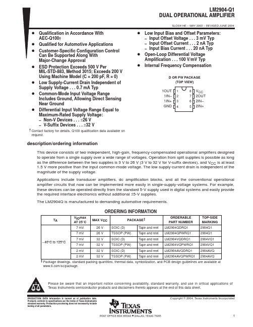
LM2902KAVQDRQ1中文资料
LM2902DR中文资料
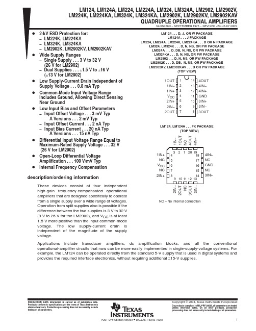
元器件交易网元器件交易网IMPORTANT NOTICETexas Instruments Incorporated and its subsidiaries (TI) reserve the right to make corrections, modifications,enhancements, improvements, and other changes to its products and services at any time and to discontinueany product or service without notice. Customers should obtain the latest relevant information before placingorders and should verify that such information is current and complete. All products are sold subject to TI’s termsand conditions of sale supplied at the time of order acknowledgment.TI warrants performance of its hardware products to the specifications applicable at the time of sale inaccordance with TI’s standard warranty. T esting and other quality control techniques are used to the extent TIdeems necessary to support this warranty. Except where mandated by government requirements, testing of allparameters of each product is not necessarily performed.TI assumes no liability for applications assistance or customer product design. Customers are responsible fortheir products and applications using TI components. T o minimize the risks associated with customer productsand applications, customers should provide adequate design and operating safeguards.TI does not warrant or represent that any license, either express or implied, is granted under any TI patent right,copyright, mask work right, or other TI intellectual property right relating to any combination, machine, or processin which TI products or services are used. Information published by TI regarding third-party products or servicesdoes not constitute a license from TI to use such products or services or a warranty or endorsement thereof.Use of such information may require a license from a third party under the patents or other intellectual propertyof the third party, or a license from TI under the patents or other intellectual property of TI.Reproduction of information in TI data books or data sheets is permissible only if reproduction is withoutalteration and is accompanied by all associated warranties, conditions, limitations, and notices. Reproductionof this information with alteration is an unfair and deceptive business practice. TI is not responsible or liable forsuch altered documentation.Resale of TI products or services with statements different from or beyond the parameters stated by TI for thatproduct or service voids all express and any implied warranties for the associated TI product or service andis an unfair and deceptive business practice. TI is not responsible or liable for any such statements.Following are URLs where you can obtain information on other Texas Instruments products and applicationsolutions:Products ApplicationsAmplifiers Audio /audioData Converters Automotive /automotiveDSP Broadband /broadbandInterface Digital Control /digitalcontrolLogic Military /militaryPower Mgmt Optical Networking /opticalnetworkMicrocontrollers Security /securityTelephony /telephonyVideo & Imaging /videoWireless /wirelessMailing Address:Texas InstrumentsPost Office Box 655303 Dallas, Texas 75265Copyright 2005, Texas Instruments Incorporated。
LM2902中文资料
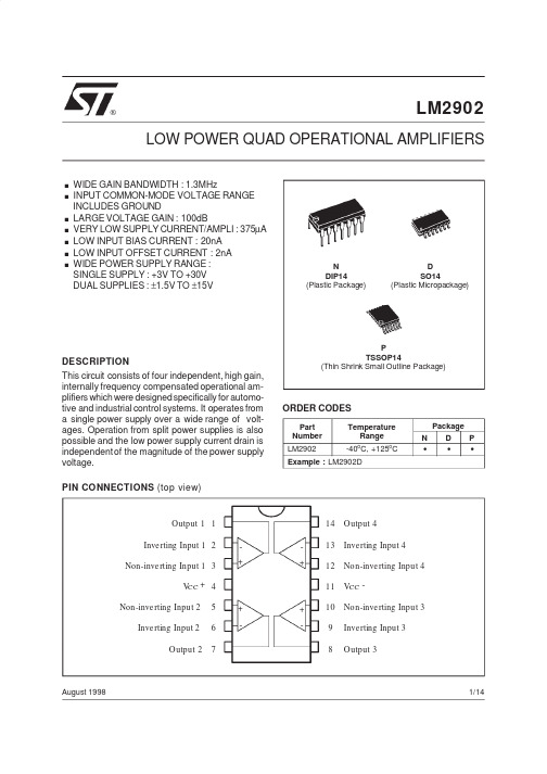
2/14
元器件交易网
LM2902
ELECTRICAL CHARACTERISTICS VCC+ = +5V, VCC– = Ground, VO = 1.4V, Tamb = +25oC (unless otherwise specified)
Symbol Vio Parameter Input Offset Voltage (note 3) o Tamb = +25 C Tmin. ≤ Tamb ≤ Tmax. Input Offset Current Tamb = +25oC Tmin. ≤ Tamb ≤ Tmax. Input Bias Current (note 2) o Tamb = +25 C Tmin. ≤ Tamb ≤ Tmax. Large Signal Voltage Gain + (VCC = +15V, RL = 2kΩ, VO = 1.4V to 11.4V) o Tamb = +25 C Tmin. ≤ Tamb ≤ Tmax. Supply Voltage Rejection Ratio (RS ≤ 10kΩ) + (VCC = 5V to 30V) o Tamb = +25 C Tmin. ≤ Tamb ≤ Tmax. Supply Current, all Amp, no load o VCC Tamb = +25 C VCC VCC Tmin. ≤ Tamb ≤ Tmax. VCC = = = = +5V +30V +5V +30V Min. Typ. 2 Max. 7 9 nA 2 30 40 nA 20 150 300 V/mV 50 25 100 dB 65 65 110 mA 0.7 1.5 0.8 1.5 1.2 3 1.2 3 V 0 0 70 60 20 10 12 80 mA 40 20 50 70 mA µA VCC -1.5 VCC -2 dB Unit mV
2902芯片资料
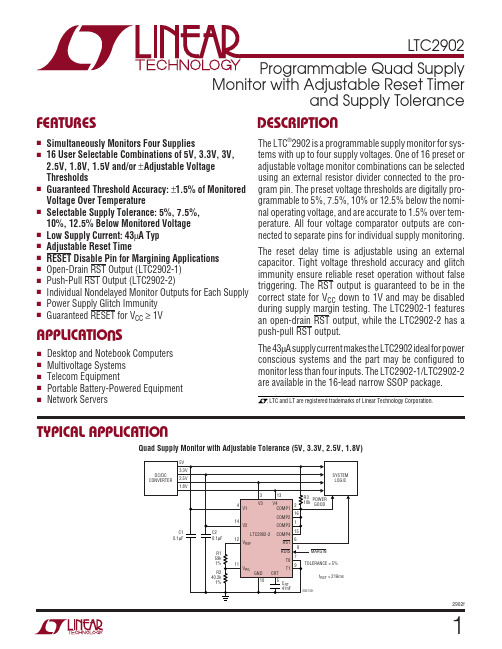
The LTC®2902 is a programmable supply monitor for systems with up to four supply voltages. One of 16 preset or adjustable voltage monitor combinations can be selected using an external resistor divider connected to the program pin. The preset voltage thresholds are digitally programmable to 5%, 7.5%, 10% or 12.5% below the nominal operating voltage, and are accurate to 1.5% over temperature. All four voltage comparator outputs are connected to separate pins for individual supply monitoring. The reset delay time is adjustable using an external capacitor. Tight voltage threshold accuracy and glitch immunity ensure reliable reset operation without false triggering. The RST output is guaranteed to be in the correct state for VCC down to 1V and may be disabled during supply margin testing. The LTC2902-1 features an open-drain RST output, while the LTC2902-2 has a push-pull RST output. The 43µA supply current makes the LTC2902 ideal for power conscious systems and the part may be configured to monitor less than four inputs. The LTC2902-1/LTC2902-2 are available in the 16-lead narrow SSOP package.
lm2904中文资料
lm2904中文资料LM2439 视频信号输出集成电路LM2453 视频信号输出集成电路LM2577 稳压集成电路LM2595 直流变换集成电路LM270H 自动增益及静噪控制集成电路LM2808N 伴音中频放大、鉴频及功率放大集成电路LM2904 双运算放大集成电路LM3065N 伴音中频放大、鉴频及前置放大集成电路LM3089 调频中频放大集成电路LM311N 电压比较运放集成电路LM317T 三端电源稳压1.5A集成电路LM324 四运算放大集成电路LM324M 四运算放大集成电路LM3361 解调集成电路LM33T 三端电源稳压-26V集成电路LM358 双运算放大集成电路LM358PS-T1 双运算放大集成电路LM3656 伴音中频放大、鉴频及前置放大集成电路LM377 双声道音频功率放大集成电路LM378 双声道音频功率放大集成电路LM380 场扫描输出集成电路LM381 运算放大集成电路LM382 宽带放大集成电路LM384 音频功率放大集成电路LM386 音频功率放大集成电路LM387 宽带放大集成电路LM3875T 音频功率放大集成电路LM3886 音频功率放大集成电路LM3915 发光二极管十位显示驱动集成电路LM399 基准稳压集成电路LM4500A 调频立体声解码集成电路LM4610 音调、音量、平衡调节集成电路LM4765 双声道音频功率放大30W×2集成电路LM741CN 运算放大集成电路LM79052 三端电源稳压-5.2V/1A集成电路LM8915N 显示驱动集成电路LN5241RA89 显示驱动集成电路LP62S512AX-70LLT 存储集成电路LPUVCP-96 端口功能扩展集成电路LR37632 伺服集成电路LR381641 主轴、字符控制集成电路LS0072 变音集成电路LSC4350 屏幕显示控制集成电路LSC4584P2 屏幕显示控制集成电路LT1074 开关电源稳压集成电路LT1109 升压稳压集成电路LTC1147 直流变换集成电路LTC1148 直流变换集成电路LTV1817 光电耦合集成电路LUKS-5140-M2 微处理集成电路LV1011 人工智能处理集成电路LV1100 音频信号处理集成电路LVA501 视频信号处理集成电路LVA521 制式切换集成电路M11B416256A 存储集成电路M1418VVW 微处理集成电路M2063SP 制式转换集成电路M208 系统控制集成电路M24C08 存储集成电路M24C128-WMN6 存储集成电路M27V201-200N6 中文字库集成电路M28F101AVPAD 存储集成电路M3004LAB1 红外遥控信号发射集成电路M32L1632512A 存储集成电路M34300-012SP 微处理集成电路M34300-628SP 微处理集成电路M34300M4-012SP 微处理集成电路M34300N4-011SP 微处理集成电路M34300N4-012SP 微处理集成电路M34300N4-555SP 微处理集成电路M34300N4-567SP 微处理集成电路M34300N4-584SP 微处理集成电路M34300N4-587SP 微处理集成电路M34300N4-628SP 微处理集成电路M34300N4-629SP 微处理集成电路M34300N4-657SP 微处理集成电路M34302M8-612SP 微处理集成电路M37100M8-616SP 微处理集成电路M37102M8-503SP 微处理集成电路M37103M4-750SP 微处理集成电路M37201M6 微处理集成电路M37204M8-852SP 微处理集成电路M37210M2-609SP 微处理集成电路M37210M3-010SP 微处理集成电路M37210M3-550SP 微处理集成电路M37210M3-603SP 微处理集成电路M37210M3-800SP 微处理集成电路M37210M3-901SP 微处理集成电路M37210M3-902SP 微处理集成电路M37210M4-650SP 微处理集成电路M37210M4-688微处理集成电路M37210M4-705SP 微处理集成电路M37210M4-786SP 微处理集成电路M37211M2-604SP 微处理集成电路M37211M2-609SP 微处理集成电路。
SD2902;中文规格书,Datasheet资料
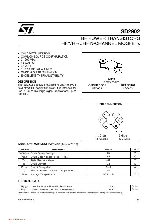
SD2902RF POWER TRANSISTORSHF/VHF/UHF N-CHANNEL MOSFETss GOLD METALLIZATIONs COMMON SOURCE CONFIGURATION s 2 - 500 MHz s 15 WATTS s 28 VOLTSs 12.5 dB MIN. AT 400 MHzs CLASS A OR AB OPERATIONsEXCELLENT THERMAL STABILITYDESCRIPTION The SD2902 is a gold metallized N-Channel MOS field-effect RF power transistor. It is intended for use in 28 V DC large signal applications up to 500 MHzNovember 1999ABSOLUTE MAXIMUM RATINGS (T case = 25 o C)THERMAL DATA®1/8SD2902ELECTRICAL SPECIFICATION (T case = 25 o C)STATICREF. 1021308K DYNAMICIMPEDANCE DATACapacitance vs Drain-Source VoltageDrain Current vs Gate VoltageMaximum Thermal Resistance vs Case TemperatureGate-Source Voltages vs Case TemperatureTYPICAL PERFORMANCESD2902Output Power vs Input PowerOutput Power vs Input PowerOutput Power vs Voltage SupplyOutput Power vs Gate VoltagePower Gain vs Output PowerEfficiency vs Output PowerTYPICAL PERFORMANCE SD2902SD2902 400 MHz Test Circuit Schematic400 MHz Test Circuit Component Part ListSD2902400 MHz Test Circuit PhotomasterProduction Test FixtureSD2902Information furnished is believed to be accurate and reliable. However, STMicroelectronics assumes no responsibility for the consequences of use of such information nor for any infringement of patents or other rights of third parties which may result from its use. No license is granted by implication or otherwise under any patent or patent rights of STMicroelectronics. Specification mentioned in this publication are subject to change without notice. This publication supersedes and replaces all information previously supplied. STMicroelectronics products are not authorized for use as critical components in life support devices or systems without express written approval of STMicroelectronics.The ST logo is a trademark of STMicroelectronics© 1999 STMicroelectronics – Printed in Italy – All Rights ReservedSTMicroelectronics GROUP OF COMPANIESAustralia - Brazil - China - Finland - France - Germany - Hong Kong - India - Italy - Japan - Malaysia - Malta - Morocco - Singapore - Spain - Sweden - Switzerland - United Kingdom - U.S.A..SD2902分销商库存信息: STMSD2902。
LM2902KAVQPWRQ1中文资料
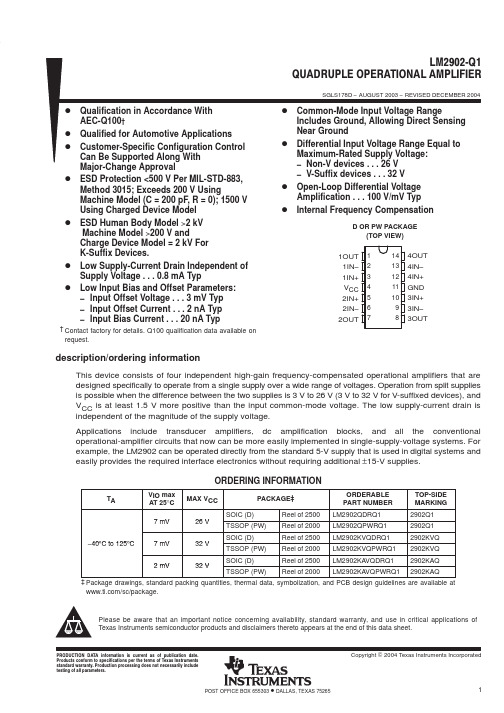
PACKAGING INFORMATIONOrderable Device Status (1)Package Type Package DrawingPins Package Qty Eco Plan (2)Lead/Ball Finish MSL Peak Temp (3)LM2902KAVQDRQ1ACTIVE SOIC D 142500Pb-Free (RoHS)CU NIPDAU Level-2-250C-1YEAR/Level-1-235C-UNLIM LM2902KAVQPWRQ1ACTIVE TSSOP PW 142000TBD CU NIPDAU Level-1-250C-UNLIM LM2902KVQDRQ1ACTIVE SOIC D 142500Pb-Free (RoHS)CU NIPDAU Level-2-250C-1YEAR/Level-1-235C-UNLIM LM2902KVQPWRQ1ACTIVE TSSOP PW 142000TBD CU NIPDAU Level-1-250C-UNLIM LM2902QDRQ1ACTIVE SOIC D 142500Pb-Free (RoHS)CU NIPDAU Level-2-250C-1YEAR/Level-1-235C-UNLIM LM2902QPWRQ1ACTIVETSSOPPW142000TBDCU NIPDAULevel-1-250C-UNLIM(1)The marketing status values are defined as follows:ACTIVE:Product device recommended for new designs.LIFEBUY:TI has announced that the device will be discontinued,and a lifetime-buy period is in effect.NRND:Not recommended for new designs.Device is in production to support existing customers,but TI does not recommend using this part in a new design.PREVIEW:Device has been announced but is not in production.Samples may or may not be available.OBSOLETE:TI has discontinued the production of the device.(2)Eco Plan -The planned eco-friendly classification:Pb-Free (RoHS),Pb-Free (RoHS Exempt),or Green (RoHS &no Sb/Br)-please check /productcontent for the latest availability information and additional product content details.TBD:The Pb-Free/Green conversion plan has not been defined.Pb-Free (RoHS):TI's terms "Lead-Free"or "Pb-Free"mean semiconductor products that are compatible with the current RoHS requirements for all 6substances,including the requirement that lead not exceed 0.1%by weight in homogeneous materials.Where designed to be soldered at high temperatures,TI Pb-Free products are suitable for use in specified lead-free processes.Pb-Free (RoHS Exempt):This component has a RoHS exemption for either 1)lead-based flip-chip solder bumps used between the die and package,or 2)lead-based die adhesive used between the die and leadframe.The component is otherwise considered Pb-Free (RoHS compatible)as defined above.Green (RoHS &no Sb/Br):TI defines "Green"to mean Pb-Free (RoHS compatible),and free of Bromine (Br)and Antimony (Sb)based flame retardants (Br or Sb do not exceed 0.1%by weight in homogeneous material)(3)MSL,Peak Temp.--The Moisture Sensitivity Level rating according to the JEDEC industry standard classifications,andpeak solder temperature.Important Information and Disclaimer:The information provided on this page represents TI's knowledge and belief as of the date that it is provided.TI bases its knowledge and belief on information provided by third parties,and makes no representation or warranty as to the accuracy of such information.Efforts are underway to better integrate information from third parties.TI has taken and continues to take reasonable steps to provide representative and accurate information but may not have conducted destructive testing or chemical analysis on incoming materials and chemicals.TI and TI suppliers consider certain information to be proprietary,and thus CAS numbers and other limited information may not be available for release.In no event shall TI's liability arising out of such information exceed the total purchase price of the TI part(s)at issue in this document sold by TI to Customer on an annual basis.PACKAGE OPTION ADDENDUM29-May-2007Addendum-Page 1IMPORTANT NOTICETexas Instruments Incorporated and its subsidiaries(TI)reserve the right to make corrections,modifications,enhancements, improvements,and other changes to its products and services at any time and to discontinue any product or service without notice. Customers should obtain the latest relevant information before placing orders and should verify that such information is current and complete.All products are sold subject to TI’s terms and conditions of sale supplied at the time of order acknowledgment.TI warrants performance of its hardware products to the specifications applicable at the time of sale in accordance with TI’s standard warranty.Testing and other quality control techniques are used to the extent TI deems necessary to support this warranty.Except where mandated by government requirements,testing of all parameters of each product is not necessarily performed.TI assumes no liability for applications assistance or customer product design.Customers are responsible for their products and applications using TI components.To minimize the risks associated with customer products and applications,customers should provide adequate design and operating safeguards.TI does not warrant or represent that any license,either express or implied,is granted under any TI patent right,copyright,mask work right,or other TI intellectual property right relating to any combination,machine,or process in which TI products or services are rmation published by TI regarding third-party products or services does not constitute a license from TI to use such products or services or a warranty or endorsement e of such information may require a license from a third party under the patents or other intellectual property of the third party,or a license from TI under the patents or other intellectual property of TI. Reproduction of information in TI data books or data sheets is permissible only if reproduction is without alteration and is accompanied by all associated warranties,conditions,limitations,and notices.Reproduction of this information with alteration is an unfair and deceptive business practice.TI is not responsible or liable for such altered documentation.Resale of TI products or services with statements different from or beyond the parameters stated by TI for that product or service voids all express and any implied warranties for the associated TI product or service and is an unfair and deceptive business practice.TI is not responsible or liable for any such statements.TI products are not authorized for use in safety-critical applications(such as life support)where a failure of the TI product would reasonably be expected to cause severe personal injury or death,unless officers of the parties have executed an agreement specifically governing such use.Buyers represent that they have all necessary expertise in the safety and regulatory ramifications of their applications,and acknowledge and agree that they are solely responsible for all legal,regulatory and safety-related requirements concerning their products and any use of TI products in such safety-critical applications,notwithstanding any applications-related information or support that may be provided by TI.Further,Buyers must fully indemnify TI and its representatives against any damages arising out of the use of TI products in such safety-critical applications.TI products are neither designed nor intended for use in military/aerospace applications or environments unless the TI products are specifically designated by TI as military-grade or"enhanced plastic."Only products designated by TI as military-grade meet military specifications.Buyers acknowledge and agree that any such use of TI products which TI has not designated as military-grade is solely at the Buyer's risk,and that they are solely responsible for compliance with all legal and regulatory requirements in connection with such use.TI products are neither designed nor intended for use in automotive applications or environments unless the specific TI products are designated by TI as compliant with ISO/TS16949requirements.Buyers acknowledge and agree that,if they use anynon-designated products in automotive applications,TI will not be responsible for any failure to meet such requirements. Following are URLs where you can obtain information on other Texas Instruments products and application solutions:Products ApplicationsAmplifiers Audio /audioData Converters Automotive /automotiveDSP Broadband /broadbandInterface Digital Control /digitalcontrolLogic Military /militaryPower Mgmt Optical Networking /opticalnetworkMicrocontrollers Security /securityRFID Telephony /telephonyLow Power /lpw Video&Imaging /videoWirelessWireless /wirelessMailing Address:Texas Instruments,Post Office Box655303,Dallas,Texas75265Copyright©2007,Texas Instruments Incorporated。
LM2900中文资料
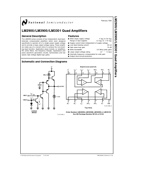
TL H 7936LM2900 LM3900 LM3301Quad AmplifiersFebruary 1995LM2900 LM3900 LM3301Quad AmplifiersGeneral DescriptionThe LM2900series consists of four independent dual input internally compensated amplifiers which were designed specifically to operate off of a single power supply voltage and to provide a large output voltage swing These amplifi-ers make use of a current mirror to achieve the non-invert-ing input function Application areas include ac amplifiers RC active filters low frequency triangle squarewave and pulse waveform generation circuits tachometers and low speed high voltage digital logic gatesFeaturesY Wide single supply voltage 4V DC to 32V DCRange or dual suppliesg 2V DC to g 16V DC Y Supply current drain independent of supply voltage Y Low input biasing current 30nA Y High open-loop gain 70dB Y Wide bandwidth 2 5MHz (unity gain)Y Large output voltage swing (V ab 1)Vp-p Y Internally frequency compensated for unity gain YOutput short-circuit protectionSchematic and Connection DiagramsTL H 7936–1Dual-In-Line and S OTL H 7936–2Top ViewOrder Number LM2900N LM3900M LM3900N or LM3301NSee NS Package Number M14A or N14AC 1995National Semiconductor Corporation RRD-B30M115 Printed in U S AAbsolute Maximum RatingsIf Military Aerospace specified devices are required please contact the National Semiconductor Sales Office Distributors for availability and specificationsLM2900 LM3900LM3301 Supply Voltage32V DC28V DCg16V DC g14V DC Power Dissipation(T A e25 C)(Note1)Molded DIP1080mW1080mWS O Package765mWInput Currents I IN a or I IN b20mA DC20mA DC Output Short-Circuit Duration One Amplifier Continuous ContinuousT A e25 C(See Application Hints)Operating Temperature Range b40 C to a85 C LM2900b40 C to a85 CLM39000 C to a70 CStorage Temperature Range b65 C to a150 C b65 C to a150 C Lead Temperature(Soldering 10sec )260 C260 C Soldering InformationDual-In-Line PackageSoldering(10sec )260 C260 C Small Outline PackageVapor Phase(60sec )215 C215 C Infrared(15sec )220 C220 CSee AN-450‘‘Surface Mounting Methods and Their Effect on Product Reliability’’for other methods of soldering surface mount devicesESD tolerance(Note7)2000V2000V Electrical Characteristics T A e25 C V a e15V DC unless otherwise statedParameter ConditionsLM2900LM3900LM3301Units Min Typ Max Min Typ Max Min Typ MaxOpen Voltage Gain Over TempV mV Loop Voltage Gain D V O e10V DC1 22 81 22 81 22 8Input Resistance Inverting Input111M XOutput Resistance889k XUnity Gain Bandwidth Inverting Input2 52 52 5MHzInput Bias Current Inverting Input V a e5V DC302003020030300nAInverting InputSlew Rate Positive Output Swing0 50 50 5V m s Negative Output Swing202020Supply Current R L e%On All Amplifiers6 2106 2106 210mA DCOutput V OUT High R L e2k I IN b e013 513 513 5Voltage V a e15 0V DC I IN a e0Swing VOUT Low I IN b e10m A0 090 20 090 20 090 2I IN a e0V DCV OUT High V a e Absolute I IN b e0Maximum Ratings I IN a e029 529 526 0R L e%Output Source618610518Current Sink(Note2)0 51 30 51 30 51 3mADC CapabilityI SINK V OL e1V I IN b e5m A5552Electrical Characteristics(Note6) V a e15V DC unless otherwise stated(Continued)Parameter ConditionsLM2900LM3900LM3301Units Min Typ Max Min Typ Max Min Typ MaxPower Supply Rejection T A e25 C f e100Hz707070dB Mirror Gain 20m A(Note3)0 901 01 10 901 01 10 9011 10m A m A 200m A(Note3)0 901 01 10 901 01 10 9011 10D Mirror Gain 20m A to200m A(Note3)252525% Mirror Current(Note4)105001050010500m A DC Negative Input Current T A e25 C(Note5)1 01 01 0mA DC Input Bias Current Inverting Input300300nA Note1 For operating at high temperatures the device must be derated based on a125 C maximum junction temperature and a thermal resistance of92 C W which applies for the device soldered in a printed circuit board operating in a still air ambient Thermal resistance for the S O package is131 C WNote2 The output current sink capability can be increased for large signal conditions by overdriving the inverting input This is shown in the section on Typical CharacteristicsNote3 This spec indicates the current gain of the current mirror which is used as the non-inverting inputNote4 Input V BE match between the non-inverting and the inverting inputs occurs for a mirror current(non-inverting input current)of approximately10m A This is therefore a typical design center for many of the application circuitsNote5 Clamp transistors are included on the IC to prevent the input voltages from swinging below ground more than approximately b0 3V DC The negative input currents which may result from large signal overdrive with capacitance input coupling need to be externally limited to values of approximately1mA Negative input currents in excess of4mA will cause the output voltage to drop to a low voltage This maximum current applies to any one of the input terminals If more than one of the input terminals are simultaneously driven negative smaller maximum currents are allowed Common-mode current biasing can be used to prevent negative input voltages see for example the‘‘Differentiator Circuit’’in the applications sectionNote6 These specs apply for b40 C s T A s a85 C unless otherwise statedNote7 Human body model 1 5k X in series with100pFApplication HintsWhen driving either input from a low-impedance source alimiting resistor should be placed in series with the inputlead to limit the peak input current Currents as large as20mA will not damage the device but the current mirror onthe non-inverting input will saturate and cause a loss of mir-ror gain at mA current levels especially at high operatingtemperaturesPrecautions should be taken to insure that the power supplyfor the integrated circuit never becomes reversed in polarityor that the unit is not inadvertently installed backwards in atest socket as an unlimited current surge through the result-ing forward diode within the IC could cause fusing of theinternal conductors and result in a destroyed unitOutput short circuits either to ground or to the positive pow-er supply should be of short time duration Units can bedestroyed not as a result of the short circuit current causingmetal fusing but rather due to the large increase in IC chipdissipation which will cause eventual failure due to exces-sive junction temperatures For example when operatingfrom a well-regulated a5V DC power supply at T A e25 C with a100k X shunt-feedback resistor(from the output tothe inverting input)a short directly to the power supply willnot cause catastrophic failure but the current magnitude willbe approximately50mA and the junction temperature willbe above T J max Larger feedback resistors will reduce thecurrent 11M X provides approximately30mA an open cir-cuit provides1 3mA and a direct connection from the out-put to the non-inverting input will result in catastrophic fail-ure when the output is shorted to V a as this then places thebase-emitter junction of the input transistor directly acrossthe power supply Short-circuits to ground will have magni-tudes of approximately30mA and will not cause cata-strophic failure at T A e25 CUnintentional signal coupling from the output to the non-in-verting input can cause oscillations This is likely only in breadboard hook-ups with long component leads and can be prevented by a more careful lead dress or by locating the non-inverting input biasing resistor close to the IC A quick check of this condition is to bypass the non-inverting input to ground with a capacitor High impedance biasing resis-tors used in the non-inverting input circuit make this input lead highly susceptible to unintentional AC signal pickupOperation of this amplifier can be best understood by notic-ing that input currents are differenced at the inverting-input terminal and this difference current then flows through the external feedback resistor to produce the output voltage Common-mode current biasing is generally useful to allow operating with signal levels near ground or even negative as this maintains the inputs biased at a V BE Internal clamp transistors(see note5)catch-negative input voltages at ap-proximately b0 3V DC but the magnitude of current flow has to be limited by the external input network For operation at high temperature this limit should be approximately100m A This new‘‘Norton’’current-differencing amplifier can be used in most of the applications of a standard IC op amp Performance as a DC amplifier using only a single supply is not as precise as a standard IC op amp operating with split supplies but is adequate in many less critical applications New functions are made possible with this amplifier which are useful in single power supply systems For example biasing can be designed separately from the AC gain as was shown in the‘‘inverting amplifier ’’the‘‘difference integra-tor’’allows controlling the charging and the discharging of the integrating capacitor with positive voltages and the‘‘fre-quency doubling tachometer’’provides a simple circuit which reduces the ripple voltage on a tachometer output DC voltage3Typical Performance CharacteristicsOpen Loop Gain Voltage Gain Voltage GainLarge Signal Frequency Input Current Supply Current ResponseOutput Sink Current Output Class-A Bias Current Output Source CurrentSupply Rejection Mirror Gain Maximum Mirror CurrentTL H 7936–94Typical Applications(V a e15V DC)Inverting AmplifierV ODC e V a 2A V j b R2R1TL H 7936–3Triangle Square GeneratorTL H 7936–4Frequency-Doubling TachometerTL H 7936–5Low V IN b V OUT Voltage RegulatorTL H 7936–6 Non-Inverting AmplifierV ODC e V a 2A V j R2R1TL H 7936–7Negative Supply BiasingV ODC eR2R3V bTL H 7936–8A V jR2R15Typical Applications (V a e 15V DC )(Continued)Low-Drift Ramp and Hold CircuitTL H 7936–10Bi-Quad Active Filter(2nd Degree State-Variable Network)TL H 7936–11Q e 50f O e 1kHz6Typical Applications(V a e15V DC)(Continued)Voltage-Controlled Current Source(Transconductance Amplifier)TL H 7936–12Hi V IN Lo(V IN b V O)Self-RegulatorQ1 Q2absorb Hi V INTL H 7936–13Ground-Referencing a Differential Input SignalTL H 7936–147Typical Applications(V a e15V DC)(Continued)Voltage Regulator(V O e V Z a V BE)TL H 7936–15Fixed Current SourcesI2e R1R2I1TL H 7936–16Voltage-Controlled Current Sink(Transconductance Amplifier)TL H 7936–17Buffer AmplifierV IN t V BETL H 7936–18TachometerTL H 7936–19V ODC e A f INAllows V O to go to zero8Typical Applications (V a e 15V DC )(Continued)Low-Voltage ComparatorNo negative voltage limit if properly biasedTL H 7936–20Power ComparatorTL H 7936–21Comparator TL H 7936–22Schmitt-TriggerTL H 7936–23Square-Wave Oscillator TL H 7936–24Pulse GeneratorTL H 7936–25Frequency Differencing TachometerV ODC e A (f 1b f 2)TL H 7936–269Typical Applications(V a e15V DC)(Continued)Frequency Averaging TachometerV ODC e A(f1a f2)TL H 7936–27Squaring Amplifier(W Hysteresis)TL H 7936–28Bi-Stable MultivibratorTL H 7936–29Differentiator(Common-Mode Biasing Keeps Input at a V BE)A V e 1 2TL H 7936–30‘‘OR’’Gatef e A a B a CTL H 7936–31‘‘AND’’Gatef e A B CTL H 7936–32Difference IntegratorTL H 7936–33 10Typical Applications (V a e 15V DC )(Continued)Low Pass Active Filterf O e 1kHzTL H 7936–34Staircase GeneratorTL H 7936–35V BE BiasingA V j bR2R1TL H 7936–36Bandpass Active FilterTL H 7936–37f o e 1kHz Q e 2511Typical Applications(V a e15V DC)(Continued)Low-Frequency MixerTL H 7936–38Free-Running Staircase Generator Pulse CounterTL H 7936–3912Typical Applications(V a e15V DC)(Continued)Supplying I IN with Aux Amp(to Allow Hi-Z Feedback Networks)TL H 7936–40One-Shot MultivibratorPW j2c106CSpeeds recoveryTL H 7936–41Non-Inverting DC Gain to(0 0)TL H 7936–4213Typical Applications(V a e15V DC)(Continued)Channel Selection by DC Control(or Audio Mixer)TL H 7936–4314Typical Applications (V a e 15V DC )(Continued)Power AmplifierTL H 7936–44One-Shot with DC Input ComparatorTL H 7936–45Trips at V IN j 0 8VaV IN must fall 0 8V aprior to t 2High Pass Active FilterTL H 7936–4615Typical Applications(V a e15V DC)(Continued)Sample-Hold and Compare with New a V INTL H 7936–47Sawtooth GeneratorTL H 7936–4816Typical Applications(V a e15V DC)(Continued)Phase-Locked LoopTL H 7936–49Boosting to300mA LoadsTL H 7936–5017Split-Supply Applications(V a e a15V DC V b e b15V DC)Non-Inverting DC GainTL H 7936–51AC AmplifierTL H 7936–5218Physical Dimensions inches(millimeters)Small Outline Package(M)Order Number LM3900MNS Package Number M14A19L M 2900 L M 3900 L M 3301Q u a d A m p l i f i e r sPhysical Dimensions inches (millimeters)(Continued)Molded Dual-In-Line Package (N)Order Number LM2900N LM3900N or LM3301NNS Package Number N14ALIFE SUPPORT POLICYNATIONAL’S PRODUCTS ARE NOT AUTHORIZED FOR USE AS CRITICAL COMPONENTS IN LIFE SUPPORT DEVICES OR SYSTEMS WITHOUT THE EXPRESS WRITTEN APPROVAL OF THE PRESIDENT OF NATIONAL SEMICONDUCTOR CORPORATION As used herein 1 Life support devices or systems are devices or 2 A critical component is any component of a life systems which (a)are intended for surgical implant support device or system whose failure to perform can into the body or (b)support or sustain life and whose be reasonably expected to cause the failure of the life failure to perform when properly used in accordance support device or system or to affect its safety or with instructions for use provided in the labeling can effectivenessbe reasonably expected to result in a significant injury to the userNational Semiconductor National Semiconductor National Semiconductor National Semiconductor CorporationEuropeHong Kong LtdJapan Ltd1111West Bardin RoadFax (a 49)0-180-530858613th Floor Straight Block Tel 81-043-299-2309。
LM2902数据手册
© 2000 National Semiconductor Corporation
DS009299
ቤተ መጻሕፍቲ ባይዱ
看中文数据手册
LM124/LM224/LM324/LM2902 Low Power Quad Operational Amplifiers
General Description
The LM124 series consists of four independent, high gain, internally frequency compensated operational amplifiers which were designed specifically to operate from a single power supply over a wide range of voltages. Operation from split power supplies is also possible and the low power supply current drain is independent of the magnitude of the power supply voltage. Application areas include transducer amplifiers, DC gain blocks and all the conventional op amp circuits which now can be more easily implemented in single power supply systems. For example, the LM124 series can be directly operated off of the standard +5V power supply voltage which is used in digital systems and will easily provide the required interface electronics without requiring the additional ± 15V power supplies.
LM2901中文资料

LM2901中⽂资料Rev 2July 20051/12LM2901Low Power Quad Voltage Comparator■Wide single supply voltage range or dualsupplies for all devices: +2V to +36V or ±1V to ±18V■Very low supply current (1.1mA) independent of supply voltage (1.4mW/comparator at +5V)■Low input bias current: 25nA typ.■Low input offset current: ±5nA typ.■Input common-mode voltage range includes ground■Low output saturation voltage:250mV typ. (I O = 4mA)■Differential input voltage range equal to the supply voltage■TTL, DTL, ECL, MOS, CMOS compatible outputsDescriptionThis device consists of four independent precision voltage comparators. All these comparators were designed specifically to operate from a single supply over a wide range of voltages. Operation from split power supplies is also possible.These comparators also have a unique characteristic in that the input common-mode voltage range includes ground even though operated from a single power supply voltage.Order CodesPart Number Temperature RangePackage Packaging Marking LM2901N-40°C, +125°C DIP14T ubeLM2901N LM2901D/LM2901DT SO-14Tube or Tape & Reel2901LM2901PT TSSOP14(Thin Shrink Outline Package)T ape & Reel 2901LM2901YD/YDTSO-14 (automotive grade level)Tube or Tape & Reel2901Y/doc/5f94010279563c1ec5da713d.htmlAbsolute Maximum Ratings LM29012/121 Absolute Maximum RatingsTable 1.Key parameters and their absolute maximum ratingsTable 2.Operating conditionsSymbol ParameterValue Unit V CC Supply Voltage±18 to 36V V ID Differential Input Voltage ±36V V IInput Voltage-0.3 to +36VOutput Short-circuit to Ground (1)1.Short-circuit from the output to V cc + can cause excessive heating and eventual destruction. The maximumoutput current is approximately 20mA, independent of the magnitude of V cc +P dPower Dissipation (2)DIP14 SO-14TSSOP142.Pd is calculated with T amb = +25°C, T j = +150°C andR thja = 80°C/W for DIP14 package R thja = 150°C/W for SO-14 package R thja = 175°C/W for TSSOP14 package 1500830710mWT J Junction Temperature +150°C T stgStorage Temperature Range -65 to +150°C ESDHBM: Human Body Model (3)3.Human body model, 100pF discharged through a 1.5k ? resistor into pin of device.1.5Kv MM: Machine Model (4)4.Machine model ESD, a 200pF cap is charged to the specified voltage, then discharged directly into the IC withno external series resistor (internal resistor < 5?), into pin to pin of device.100V CDM: Charged Device Model1500VSymbol ParameterValue Unit V CC Supply Voltage2 to 32±1 to ±16V V icm Common Mode Input Voltage Range 0 to (V CC + -1.5)V T operOperating Free-Air T emperature range-40 to +125°CLM2901Typical Application Schematics 2 Typical Application Schematics3/124/123 Electrical CharacteristicsTable 3.V CC + = 5V, V cc - = GND, T amb = 25°C (unless otherwise specified)Symbol ParameterMin.Typ.Max.Unit V ioInput Offset Voltage (1)T amb = +25°CT min ≤ T amb ≤ T max.1. At output switch point, VO ≈ 1.4V, RS = 0 with VCC + from 5V to 30V, and over the full input common-moderange (0V to VCC + –1.5V).1715mVI ioInput Offset Current T amb = +25°CT min ≤ T amb ≤ T max.550150nAI ibInput Bias Current (I I + or I I -) (2)T amb = 2.5VT min ≤ T amb ≤ T max.2.The direction of the input current is out of the IC due to the PNP input stage. This current is essentiallyconstant, independent of the state of the output, so no loading charge exists on the reference of input lines 25250400nAA vd Large Signal Voltage Gain(V cc = 15V ,R L =15k ?, V o =1 to 11V) 25200V/mVI ccSupply Current (all comparators))V CC = +5V, no load V CC = +30V, no load1.11.322.5mAV icm Input Common Mode Voltage Range (V cc = 30V)(3)T amb = +25°CT min ≤ T amb ≤ T max.3.The input common-mode voltage of either input signal voltage should not be allowed to go negative by morethan 0.3V. The upper end of the common-mode voltage range is VCC + –1.5V, but either or both inputs can go to +30V without damage.00V CC +-1.5V CC +-2V V idDifferential Input Voltage (4)4.The response time specified is for a 100mV input step with 5mV overdrive.V CC +VV OLLow Level Output Voltage V id = -1V , I sink = 4mA T amb = +25°CT min ≤ T amb ≤ T max 250400700mVI oh High Level Output Current (V CC =V o =30V, V id = 1V)T amb = +25°CT min ≤ T amb ≤ T max0.11nA µA I sink Output Sink Current (V id = -1V,V o = 1.5V)616mA t reSmall Signal Response Time (5)(R L = 5.1k ? connected to V CC + 5.Positive excursions of input voltage may exceed the power supply level. As long as the other voltage remainswithin the common-mode range, the comparator will provide a proper output state. The low input voltage state must not be less than –0.3V (or 0.3V bellow the negative power supply, if used) 1.3µst relLarge Signal Response Time (6)TTL Input (V ref = +1.4 V, R L =5.1k ? to V CC +)Output Signal at 50% of final value Output Signal at 95% of final value 6.Maximum values are guaranteed by design.5001ns µsFigure 3.Supply current versus supplyFigure 4.Input current versus supply voltageFigure 6.Response time for various input5/12Typical Applications LM29014 Typical ApplicationsLM2901Typical Applications7/12Figure 14.Low frequency op- amp with offsetFigure 15.Zero crossing detector (singleFigure 16.Limit comparatorFigure 17.Split-supply applications - zeroFigure 18.Crystal controlled oscillatorFigure /doc/5f94010279563c1ec5da713d.html parator with a negative Typical Applications LM29018/12LM2901PACKAGE MECHANICAL DATA 5 PACKAGE MECHANICAL DATA9/12PACKAGE MECHANICAL DATA LM290110/125.2 SO-14 packageLM2901PACKAGE MECHANICAL DATA11/125.3 TSSOP14 packageRevision History LM290112/126 Revision HistoryDate RevisionChangesJan. 20021Initial release.July 20051 - PPAP references inserted in the datasheet see Table : Order Codeson page 1.2 - ESD protection inserted in T able 1 on page 2.Information furnished is believed to be accurate and reliable. However, STMicroelectronics assumes no responsibility for the consequences of use of such information nor for any infringement of patents or other rights of third parties which may result from its use. No license is granted by implication or otherwise under any patent or patent rights of STMicroelectronics. Specifications mentioned in this publication are subject to change without notice. This publication supersedes and replaces all information previously supplied. STMicroelectronics products are not authorized for use as critical components in life support devices or systems without express written approval of STMicroelectronics.The ST logo is a registered trademark of STMicroelectronics.All other names are the property of their respective owners2005 STMicroelectronics - All rights reservedSTMicroelectronics group of companiesAustralia - Belgium - Brazil - Canada - China - Czech Republic - Finland - France - Germany - Hong Kong - India - Israel -Italy - Japan -Malaysia - Malta - Morocco - Singapore - Spain - Sweden - Switzerland - United Kingdom - United States of America /doc/5f94010279563c1ec5da713d.html。
LM2904-Q1中文资料
PACKAGING INFORMATIONOrderable Device Status (1)Package Type Package DrawingPins Package Qty Eco Plan (2)Lead/Ball Finish MSL Peak Temp (3)LM2904AVQDRQ1ACTIVE SOIC D 82500Pb-Free (RoHS)CU NIPDAU Level-2-250C-1YEAR/Level-1-235C-UNLIM LM2904AVQPWRQ1ACTIVE TSSOP PW 82000None CU NIPDAU Level-1-250C-UNLIM LM2904QDRQ1ACTIVE SOIC D 82500Pb-Free (RoHS)CU NIPDAU Level-2-250C-1YEAR/Level-1-235C-UNLIM LM2904QPWRQ1ACTIVE TSSOP PW 82000None CU NIPDAU Level-1-250C-UNLIM LM2904VQDRQ1ACTIVE SOIC D 82500Pb-Free (RoHS)CU NIPDAU Level-2-250C-1YEAR/Level-1-235C-UNLIM LM2904VQPWRQ1ACTIVETSSOPPW82000NoneCU NIPDAULevel-1-250C-UNLIM(1)The marketing status values are defined as follows:ACTIVE:Product device recommended for new designs.LIFEBUY:TI has announced that the device will be discontinued,and a lifetime-buy period is in effect.NRND:Not recommended for new designs.Device is in production to support existing customers,but TI does not recommend using this part in a new design.PREVIEW:Device has been announced but is not in production.Samples may or may not be available.OBSOLETE:TI has discontinued the production of the device.(2)Eco Plan -May not be currently available -please check /productcontent for the latest availability information and additional product content details.None:Not yet available Lead (Pb-Free).Pb-Free (RoHS):TI's terms "Lead-Free"or "Pb-Free"mean semiconductor products that are compatible with the current RoHS requirements for all 6substances,including the requirement that lead not exceed 0.1%by weight in homogeneous materials.Where designed to be soldered at high temperatures,TI Pb-Free products are suitable for use in specified lead-free processes.Green (RoHS &no Sb/Br):TI defines "Green"to mean "Pb-Free"and in addition,uses package materials that do not contain halogens,including bromine (Br)or antimony (Sb)above 0.1%of total product weight.(3)MSL,Peak Temp.--The Moisture Sensitivity Level rating according to the JEDECindustry standard classifications,and peak solder temperature.Important Information and Disclaimer:The information provided on this page represents TI's knowledge and belief as of the date that it is provided.TI bases its knowledge and belief on information provided by third parties,and makes no representation or warranty as to the accuracy of such information.Efforts are underway to better integrate information from third parties.TI has taken and continues to take reasonable steps to provide representative and accurate information but may not have conducted destructive testing or chemical analysis on incoming materials and chemicals.TI and TI suppliers consider certain information to be proprietary,and thus CAS numbers and other limited information may not be available for release.In no event shall TI's liability arising out of such information exceed the total purchase price of the TI part(s)at issue in this document sold by TI to Customer on an annual basis.PACKAGE OPTION ADDENDUM4-Mar-2005Addendum-Page 1元器件交易网IMPORTANT NOTICETexas Instruments Incorporated and its subsidiaries (TI) reserve the right to make corrections, modifications,enhancements, improvements, and other changes to its products and services at any time and to discontinueany product or service without notice. Customers should obtain the latest relevant information before placingorders and should verify that such information is current and complete. All products are sold subject to TI’s termsand conditions of sale supplied at the time of order acknowledgment.TI warrants performance of its hardware products to the specifications applicable at the time of sale inaccordance with TI’s standard warranty. T esting and other quality control techniques are used to the extent TIdeems necessary to support this warranty. Except where mandated by government requirements, testing of allparameters of each product is not necessarily performed.TI assumes no liability for applications assistance or customer product design. Customers are responsible fortheir products and applications using TI components. T o minimize the risks associated with customer productsand applications, customers should provide adequate design and operating safeguards.TI does not warrant or represent that any license, either express or implied, is granted under any TI patent right,copyright, mask work right, or other TI intellectual property right relating to any combination, machine, or processin which TI products or services are used. Information published by TI regarding third-party products or servicesdoes not constitute a license from TI to use such products or services or a warranty or endorsement thereof.Use of such information may require a license from a third party under the patents or other intellectual propertyof the third party, or a license from TI under the patents or other intellectual property of TI.Reproduction of information in TI data books or data sheets is permissible only if reproduction is withoutalteration and is accompanied by all associated warranties, conditions, limitations, and notices. Reproductionof this information with alteration is an unfair and deceptive business practice. TI is not responsible or liable forsuch altered documentation.Resale of TI products or services with statements different from or beyond the parameters stated by TI for thatproduct or service voids all express and any implied warranties for the associated TI product or service andis an unfair and deceptive business practice. TI is not responsible or liable for any such statements.Following are URLs where you can obtain information on other Texas Instruments products and applicationsolutions:Products ApplicationsAmplifiers Audio /audioData Converters Automotive /automotiveDSP Broadband /broadbandInterface Digital Control /digitalcontrolLogic Military /militaryPower Mgmt Optical Networking /opticalnetworkMicrocontrollers Security /securityTelephony /telephonyVideo & Imaging /videoWireless /wirelessMailing Address:Texas InstrumentsPost Office Box 655303 Dallas, Texas 75265Copyright 2005, Texas Instruments Incorporated。
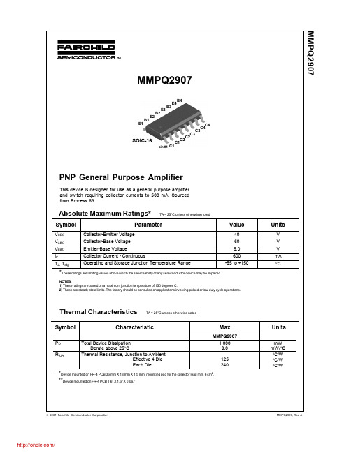
MMPQ2907;中文规格书,Datasheet资料
Base-Emitter Saturation Voltage vs Collector Current
1 0.8 0.6
125 ºC - 40 ºC 25 °C
Base Emitter ON Voltage vs Collector Current
1 0.8
- 40 ºC
0.6 0.4 0.2 0 0.1
1 KW
37 W
1.0 KW 0 - 30 V 50 W
£ 200ns
FIGURE 2: Saturated Turn-Off Switching Time Test Circuit
/
TRADEMARKS
The following are registered and unregistered trademarks Fairchild Semiconductor owns or is authorized to use and is not intended to be an exhaustive list of all such trademarks.
MMPQ2907
MMPQ2907
E3 B3 E4 B4
E1
B1
E2
B2
SOIC-16
pin #1 C1
C2 C1
C3 C2
C4 C4 C3
PNP General Purpose Amplifier
This device is designed for use as a general purpose amplifier and switch requiring collector currents to 500 mA. Sourced from Process 63.
LM2902PWR芯片资料

2
POST OFFICE BOX 655303
• DALLAS, TEXAS 75265
LM124, LM124A, LM224, LM224A, LM324, LM324A, LM2902, LM2902V, LM224K, LM224KA, LM324K, LM324KA, LM2902K, LM2902KV, LM2902KAV QUADRUPLE OPERATIONAL AMPLIFIERS
SLOS066R − SEPTEMBER 1975 − REVISED JANUARY 2005
1IN+ NC VCC NC 2IN+
4 5 6 7 8
3 2 1 20 19 18 17 16 15 14 9 10 11 12 13
1IN− 1OUT NC 4OUT 4IN− 4IN+ NC GND NC 3IN+
NC − No internal connection
On products compliant to MIL PRF 38535, all parameters are tested unless otherwise noted. On all other products, production processing does not necessarily include testing of all parameters.
PRODUCTION DATA information is current as of publication date. Products conform to specifications per the terms of Texas Instruments standard warranty. Production processing does not necessarily include testing of all parameters.
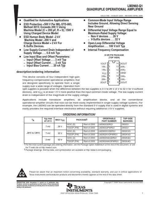
LM2902QDRQ1中文资料
PACKAGING INFORMATIONOrderable Device Status(1)PackageType PackageDrawingPins PackageQtyEco Plan(2)Lead/Ball Finish MSL Peak Temp(3)LM2902KAVQDRG4Q1ACTIVE SOIC D142500Green(RoHS&no Sb/Br)CU NIPDAU Level-1-260C-UNLIMLM2902KAVQDRQ1ACTIVE SOIC D142500Pb-Free(RoHS)CU NIPDAU Level-2-250C-1YEAR/Level-1-235C-UNLIMLM2902KAVQPWRG4Q1ACTIVE TSSOP PW142000Green(RoHS&no Sb/Br)CU NIPDAU Level-1-260C-UNLIMLM2902KAVQPWRQ1ACTIVE TSSOP PW142000Green(RoHS&no Sb/Br)CU NIPDAU Level-1-260C-UNLIMLM2902KVQDRG4Q1ACTIVE SOIC D142500Green(RoHS&no Sb/Br)CU NIPDAU Level-1-260C-UNLIMLM2902KVQDRQ1ACTIVE SOIC D142500Pb-Free(RoHS)CU NIPDAU Level-2-250C-1YEAR/Level-1-235C-UNLIMLM2902KVQPWRG4Q1ACTIVE TSSOP PW142000Green(RoHS&no Sb/Br)CU NIPDAU Level-1-260C-UNLIM LM2902KVQPWRQ1ACTIVE TSSOP PW142000TBD CU NIPDAU Level-1-250C-UNLIM LM2902QDRG4Q1ACTIVE SOIC D142500Green(RoHS&no Sb/Br)CU NIPDAU Level-1-260C-UNLIMLM2902QDRQ1ACTIVE SOIC D142500Pb-Free(RoHS)CU NIPDAU Level-2-250C-1YEAR/Level-1-235C-UNLIMLM2902QPWRG4Q1ACTIVE TSSOP PW142000Green(RoHS&no Sb/Br)CU NIPDAU Level-1-260C-UNLIM LM2902QPWRQ1ACTIVE TSSOP PW142000TBD CU NIPDAU Level-1-250C-UNLIM (1)The marketing status values are defined as follows:ACTIVE:Product device recommended for new designs.LIFEBUY:TI has announced that the device will be discontinued,and a lifetime-buy period is in effect.NRND:Not recommended for new designs.Device is in production to support existing customers,but TI does not recommend using this part in a new design.PREVIEW:Device has been announced but is not in production.Samples may or may not be available.OBSOLETE:TI has discontinued the production of the device.(2)Eco Plan-The planned eco-friendly classification:Pb-Free(RoHS),Pb-Free(RoHS Exempt),or Green(RoHS&no Sb/Br)-please check /productcontent for the latest availability information and additional product content details.TBD:The Pb-Free/Green conversion plan has not been defined.Pb-Free(RoHS):TI's terms"Lead-Free"or"Pb-Free"mean semiconductor products that are compatible with the current RoHS requirements for all6substances,including the requirement that lead not exceed0.1%by weight in homogeneous materials.Where designed to be soldered at high temperatures,TI Pb-Free products are suitable for use in specified lead-free processes.Pb-Free(RoHS Exempt):This component has a RoHS exemption for either1)lead-based flip-chip solder bumps used between the die and package,or2)lead-based die adhesive used between the die and leadframe.The component is otherwise considered Pb-Free(RoHS compatible)as defined above.Green(RoHS&no Sb/Br):TI defines"Green"to mean Pb-Free(RoHS compatible),and free of Bromine(Br)and Antimony(Sb)based flame retardants(Br or Sb do not exceed0.1%by weight in homogeneous material)(3)MSL,Peak Temp.--The Moisture Sensitivity Level rating according to the JEDEC industry standard classifications,and peak solder temperature.Important Information and Disclaimer:The information provided on this page represents TI's knowledge and belief as of the date that it is provided.TI bases its knowledge and belief on information provided by third parties,and makes no representation or warranty as to the accuracy of such information.Efforts are underway to better integrate information from third parties.TI has taken and continues to take reasonable steps to provide representative and accurate information but may not have conducted destructive testing or chemical analysis on incoming materials and chemicals.TI and TI suppliers consider certain information to be proprietary,and thus CAS numbers and other limited information may not be available for release.In no event shall TI's liability arising out of such information exceed the total purchase price of the TI part(s)at issue in this document sold by TIto Customer on an annual basis.OTHER QUALIFIED VERSIONS OF LM2902-Q1:•Catalog:LM2902•Enhanced Product:LM2902-EPNOTE:Qualified Version Definitions:•Catalog-TI's standard catalog product•Enhanced Product-Supports Defense,Aerospace and Medical Applications元器件交易网IMPORTANT NOTICETexas Instruments Incorporated and its subsidiaries(TI)reserve the right to make corrections,modifications,enhancements,improvements, and other changes to its products and services at any time and to discontinue any product or service without notice.Customers should obtain the latest relevant information before placing orders and should verify that such information is current and complete.All products are sold subject to TI’s terms and conditions of sale supplied at the time of order acknowledgment.TI warrants performance of its hardware products to the specifications applicable at the time of sale in accordance with TI’s standard warranty.Testing and other quality control techniques are used to the extent TI deems necessary to support this warranty.Except where mandated by government requirements,testing of all parameters of each product is not necessarily performed.TI assumes no liability for applications assistance or customer product design.Customers are responsible for their products and applications using TI components.To minimize the risks associated with customer products and applications,customers should provide adequate design and operating safeguards.TI does not warrant or represent that any license,either express or implied,is granted under any TI patent right,copyright,mask work right, or other TI intellectual property right relating to any combination,machine,or process in which TI products or services are rmation published by TI regarding third-party products or services does not constitute a license from TI to use such products or services or a warranty or endorsement e of such information may require a license from a third party under the patents or other intellectual property of the third party,or a license from TI under the patents or other intellectual property of TI.Reproduction of TI information in TI data books or data sheets is permissible only if reproduction is without alteration and is accompanied by all associated warranties,conditions,limitations,and notices.Reproduction of this information with alteration is an unfair and deceptive business practice.TI is not responsible or liable for such altered rmation of third parties may be subject to additional restrictions.Resale of TI products or services with statements different from or beyond the parameters stated by TI for that product or service voids all express and any implied warranties for the associated TI product or service and is an unfair and deceptive business practice.TI is not responsible or liable for any such statements.TI products are not authorized for use in safety-critical applications(such as life support)where a failure of the TI product would reasonably be expected to cause severe personal injury or death,unless officers of the parties have executed an agreement specifically governing such use.Buyers represent that they have all necessary expertise in the safety and regulatory ramifications of their applications,and acknowledge and agree that they are solely responsible for all legal,regulatory and safety-related requirements concerning their products and any use of TI products in such safety-critical applications,notwithstanding any applications-related information or support that may be provided by TI.Further,Buyers must fully indemnify TI and its representatives against any damages arising out of the use of TI products in such safety-critical applications.TI products are neither designed nor intended for use in military/aerospace applications or environments unless the TI products are specifically designated by TI as military-grade or"enhanced plastic."Only products designated by TI as military-grade meet military specifications.Buyers acknowledge and agree that any such use of TI products which TI has not designated as military-grade is solely at the Buyer's risk,and that they are solely responsible for compliance with all legal and regulatory requirements in connection with such use. TI products are neither designed nor intended for use in automotive applications or environments unless the specific TI products are designated by TI as compliant with ISO/TS16949requirements.Buyers acknowledge and agree that,if they use any non-designated products in automotive applications,TI will not be responsible for any failure to meet such requirements.Following are URLs where you can obtain information on other Texas Instruments products and application solutions:Products ApplicationsAmplifiersAudioData Converters AutomotiveDSP BroadbandClocks and Timers Digital ControlInterface MedicalLogic MilitaryPower Mgmt Optical NetworkingMicrocontrollers SecurityRFID TelephonyRF/IF and ZigBee®Solutions Video&ImagingWirelessMailing Address:Texas Instruments,Post Office Box655303,Dallas,Texas75265Copyright©2008,Texas Instruments Incorporated元器件交易网。
LM2902M中文资料

200 500 VCC -2.0 100 -
µV/°C nA pA/°C nA V V/mV V V mV mA
Output Voltage Swing
VO(H) VO(L)
VCC = 5V, RL=10kΩ
VI(+) = 1V, VI(-) ISOURCE = 0V VCC = 15V, VO(P) = 2V Output Current ISINK Differential Input Voltage VI(+) = 0V, VI(-) = 1V VCC = 15V, VO(P) = 2V -
Q17 Q19
Q20 Q2 IN(-) Q1 R2 IN(+) Q11 Q21 Q7 Q8 Q9 Q10 Q13 Q15 Q14 Q16 OUTPUT Q3 Q4 C1 Q18 R1
GND
Absolute Maximum Ratings
Parameter Power Supply Voltage Differential Input Voltage Input Voltage Output Short Circuit to GND Vcc≤15V, TA=25°C(one Amp) Power Dissipation, TA=25°C 14-DIP 14-SOP Operating Temperature Range Storage Temperature Range Symbol VCC VI(DIFF) VI PD TOPR TSTG LM224/LM224A ±16 or 32 32 -0.3 to +32 Continuous 1310 640 -25 ~ +85 -65 ~ +150 LM324/LM324A ±16 or 32 32 -0.3 to +32 Continuous 1310 640 0 ~ +70 -65 ~ +150 LM2902 ±13 or 26 26 -0.3 to +26 Continuous 1310 640 -40 ~ +85 -65 ~ +150 Unit V V V mW °C °C
LM2902KVQPWRG4,LM224ADRG4,LM2902KDRG4,LM2902KPWRG4,LM224ADG4,LM2902KNSRG4, 规格书,Datasheet 资料
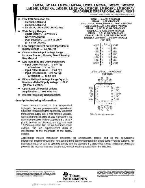
1POST OFFICE BOX 655303 •DALLAS, TEXAS 75265(26 V for LM2902)− Dual Supplies ...+1.5 V to +16 V (+13 V for LM2902)D Low Supply-Current Drain Independent of Supply Voltage ...0.8 mA TypD Common-Mode Input Voltage RangeIncludes Ground, Allowing Direct Sensing Near GroundDLow Input Bias and Offset Parameters − Input Offset Voltage ...3mV TypA Versions ...2mV Typ− Input Offset Current ...2 nA Typ − Input Bias Current ...20 nA TypA Versions ...15 nA TypD Differential Input Voltage Range Equal toMaximum-Rated Supply Voltage ...32V (26 V for LM2902)DOpen-Loop Differential Voltage Amplification ...100 V/mV Typ DInternal Frequency Compensationdescription/ordering information These devices consist of four independenthigh-gain frequency-compensated operational amplifiers that are designed specifically to operate from a single supply over a wide range of voltages.Operation from split supplies also is possible if the difference between the two supplies is 3 V to 32 V (3 V to 26 V for the LM2902), and V CC is at least 1.5 V more positive than the input common-mode voltage. The low supply-current drain is independent of the magnitude of the supply voltage.Applications include transducer amplifiers, dc amplification blocks, and all the conventional operational-amplifier circuits that now can be more easily implemented in single-supply-voltage systems. For example, the LM124 can be operated directly from the standard 5-V supply that is used in digital systems and provides the required interface electronics, without requiring additional ±15-V supplies.PRODUCTION DATA information is current as of publication date.Products conform to specifications per the terms of Texas Instruments standard warranty. Production processing does not necessarily include testing of all parameters.1234 5671413121110981OUT 1IN−1IN+V CC 2IN+2IN−2OUT4OUT 4IN−4IN+GND 3IN+3IN−3OUTLM2902K ...D, DB, N, NS, OR PW PACKAGE LM2902KV, LM2902KAV ...D OR PW PACKAGE(TOP VIEW)32120199101112134567818171615144IN+NC GND NC 3IN+1IN+NC V CC NC 2IN+LM124, LM124A ...FK PACKAGE(TOP VIEW)1I N −1O U T N C 3I N −4I N −2I N −2O U T N C NC − No internal connection3O U T 4O U T On products compliant to MIL-PRF-38535, all parameters are tested unless otherwise noted. On all other products,production processing does not necessarily include testing of all parameters.LM124, LM124A, LM224, LM224A, LM324, LM324A, LM2902, LM2902V,LM224K, LM224KA, LM324K, LM324KA, LM2902K, LM2902KV, LM2902KAV QUADRUPLE OPERATIONAL AMPLIFIERSSLOS066T − SEPTEMBER 1975 − REVISED MARCH 20102POST OFFICE BOX 655303 •DALLAS, TEXAS 75265ORDERING INFORMATION {T AV IO max AT 25°CMAX TESTED V CCPACKAGE }ORDERABLEPART NUMBER TOP-SIDE MARKING PDIP (N)Tube of 25LM324N LM324N PDIP (N)Tube of 25LM324KN LM324KNTube of 50LM324D Reel of 2500LM324DR Reel of 2500LM324DRG3LM324SOIC (D)Tube of 50LM324KD 7mV 30V Reel of 2500LM324KDR LM324K 7 mV 30 VReel of 2000LM324NSR LM324Tube of 50LM324KNS SOP (NS)Reel of 2000LM324KNSR LM324K Tube of 90LM324PW TSSOP (PW)Reel of 2000LM324PWR L324TSSOP (PW)Tube of 90LM324KPW C to 70Reel of 2000LM324KPWR L324K 0°C to 70°CPDIP (N)Tube of 25LM324AN LM324AN PDIP (N)Tube of 25LM324KAN LM324KAN Tube of 50LM324AD SOIC (D)Reel of 2500LM324ADR LM324A SOIC (D)Tube of 50LM324KAD Reel of 2500LM324KADR LM324KA 3mV 30V Reel of 2000LM324ANSR LM324A 3 mV 30 VTube of 50LM324KANS SOP (NS)Reel of 2000LM324KANSR LM324KA SSOP (DB)Reel of 2000LM324ADBR LM324A Tube of 90LM324APW TSSOP (PW)Reel of 2000LM324APWR L324A TSSOP (PW)Tube of 90LM324KAPW Reel of 2000LM324KAPWR L324KA PDIP (N)Tube of 25LM224N LM224N PDIP (N)Tube of 25LM224KN LM224KN 5mV 30V Tube of 50LM224D 5 mV30 VSOIC (D)Reel of 2500LM224DR LM224SOIC (D)Tube of 50LM224KD 25C to 85Reel of 2500LM224KDR LM224K −25°C to 85°CPDIP (N)Tube of 25LM224AN LM224AN PDIP (N)Tube of 25LM224KAN LM224KAN 3mV 30V Tube of 50LM224AD 3 mV30 VSOIC (D)Reel of 2500LM224ADR LM224A SOIC (D)Tube of 50LM224KAD Reel of 2500LM224KADRLM224KA †For the most current package and ordering information, see the Package Option Addendum at the end of this document, or see the TIweb site at .‡Package drawings, thermal data, and symbolization are available at /packaging.LM124, LM124A, LM224, LM224A, LM324, LM324A, LM2902, LM2902V,LM224K, LM224KA, LM324K, LM324KA, LM2902K, LM2902KV, LM2902KAVQUADRUPLE OPERATIONAL AMPLIFIERSSLOS066T − SEPTEMBER 1975 − REVISED MARCH 20103POST OFFICE BOX 655303 •DALLAS, TEXAS 75265ORDERING INFORMATION (CONTINUED)T AV IO max AT 25°CMAX TESTED V CCPACKAGE †ORDERABLEPART NUMBER TOP-SIDE MARKING PDIP (N)Tube of 25LM2902N LM2902N PDIP (N)Tube of 25LM2902KN LM2902KN Tube of 50LM2902D SOIC (D)Reel of 2500LM2902DR LM2902SOIC (D)Tube of 50LM2902KD Reel of 2500LM2902KDR LM2902K Reel of 2000LM2902NSR LM2902Tube of 50LM2902KNS 7 mV26 VSOP (NS)Reel of 2000LM2902KNSR LM2902K −40°C to 125°CSSOP (DB)Tube of 80LM2902KDB 40SSOP (DB)Reel of 2000LM2902KDBR L2902K Tube of 90LM2902PW TSSOP (PW)Reel of 2000LM2902PWR L2902TSSOP (PW)Tube of 90LM2902KPW Reel of 2000LM2902KPWR L2902K 32V SOIC (D)Reel of 2500LM2902KVQDR L2902KV 32 VTSSOP (PW)Reel of 2000LM2902KVQPWR L2902KV 2mV 32V SOIC (D)Reel of 2500LM2902KAVQDR L2902KA 2 mV32 VTSSOP (PW)Reel of 2000LM2902KAVQPWR L2902KA CDIP (J)Tube of 25LM124J LM124J CFP (W)Tube of 25LM124W LM124W LCCC (FK)Tube of 55LM124FK LM124FK 55C to 125 5 mV30 VSOIC (D)Tube of 50LM124D −55°C to 125°CSOIC (D)Reel of 2500LM124DR LM124CDIP (J)Tube of 25LM124AJ LM124AJ 2 mV30 V CFP (W)Tube of 25 LM124AW LM124AW LCCC (FK)Tube of 55LM124AFKLM124AFK†Package drawings, standard packing quantities, thermal data, symbolization, and PCB design guidelines are available at /sc/package.symbol (each amplifier)−+IN−IN+OUTLM124, LM124A, LM224, LM224A, LM324, LM324A, LM2902, LM2902V,LM224K, LM224KA, LM324K, LM324KA, LM2902K, LM2902KV, LM2902KAV QUADRUPLE OPERATIONAL AMPLIFIERSSLOS066T − SEPTEMBER 1975 − REVISED MARCH 20104POST OFFICE BOX 655303 •DALLAS, TEXAS 75265schematic (each amplifier)V CCOUTGNDIN−IN+COMPONENT COUNT(total device)Epi-FET Transistors Diodes Resistors Capacitors1954114†ESD protection cells - available on LM324K and LM324KA onlyLM124, LM124A, LM224, LM224A, LM324, LM324A, LM2902, LM2902V,LM224K, LM224KA, LM324K, LM324KA, LM2902K, LM2902KV, LM2902KAVQUADRUPLE OPERATIONAL AMPLIFIERSSLOS066T − SEPTEMBER 1975 − REVISED MARCH 20105POST OFFICE BOX 655303 •DALLAS, TEXAS 75265absolute maximum ratings over operating free-air temperature range (unless otherwise noted)†LM2902ALL OTHER DEVICES UNIT Supply voltage, V CC (see Note 1)±13 or 26±16 or 32V Differential input voltage, V ID (see Note 2)±26±32V Input voltage, V I (either input)−0.3 to 26−0.3 to 32VDuration of output short circuit (one amplifier) to ground at (or below) T A = 25°C, V CC ≤ 15 V (see Note 3)UnlimitedUnlimitedD package 8686DB package9696θN package 8080°C/WPackage thermal impedance, JA (see Notes 4 and 5)NS package 7676PW package 113113FK package5.61q J package 15.05°C/W Package thermal impedance, JC (see Notes 6 and 7)W package14.65Operating virtual junction temperature, T J 150150°C Case temperature for 60 secondsFK package 260°C Lead temperature 1,6 mm (1/16 inch) from case for 60 seconds J or W package300300°C Storage temperature range, T stg−65 to 150−65 to 150°C†Stresses beyond those listed under “absolute maximum ratings” may cause permanent damage to the device. These are stress ratings only, and functional operation of the device at these or any other conditions beyond those indicated under “recommended operating conditions” is not implied. Exposure to absolute-maximum-rated conditions for extended periods may affect device reliability.NOTES: 1.All voltage values (except differential voltages and V CC specified for the measurement of I OS ) are with respect to the network GND.2.Differential voltages are at IN+, with respect to IN−.3.Short circuits from outputs to V CC can cause excessive heating and eventual destruction.4.Maximum power dissipation is a function of T J (max), q JA , and T A . The maximum allowable power dissipation at any allowableambient temperature is P D = (T J (max) − T A )/q JA . Operating at the absolute maximum T J of 150°C can affect reliability.5.The package thermal impedance is calculated in accordance with JESD 51-7.6.Maximum power dissipation is a function of T J (max), q JC , and T C . The maximum allowable power dissipation at any allowable casetemperature is P D = (T J (max) − T C )/q JC . Operating at the absolute maximum T J of 150°C can affect reliability.7.The package thermal impedance is calculated in accordance with MIL-STD-883.ESD protectionTEST CONDITIONSTYP UNIT Human-Body ModelLM224K, LM224KA, LM324K, LM324KA, LM2902K, LM2902KV, LM2902KAV±2kVLM124, LM124A, LM224, LM224A, LM324, LM324A, LM2902, LM2902V,LM224K, LM224KA, LM324K, LM324KA, LM2902K, LM2902KV, LM2902KAV QUADRUPLE OPERATIONAL AMPLIFIERSSLOS066T − SEPTEMBER 1975 − REVISED MARCH 20106POST OFFICE BOX 655303 •DALLAS, TEXAS 75265electrical characteristics at specified free-air temperature, V CC = 5 V (unless otherwise noted)‡LM124LM224LM324LM324KPARAMETERTEST CONDITIONS †T AMINTYP §MAXMINTYP §MAXUNITInput offset voltage 25°C 3537V IO Input offset voltage V CC = 5 V to MAX,V IC = V ICR min,V O = 1.4 V Full range 79mV Input offset current 14V 25°C 230250I IO Input offset current V O = 1.4 V Full range 100150nA Input bias current V 14V25°C −20−150−20−250I IBInput bias currentO = 1.4 V Full range −300−500nA5V to MAX 25°C0 to V CC − 1.50 to V CC − 1.5V ICRCommon-mode input voltage rangeV CC = 5 V to MAXFull range 0 to 0 to VFull rangeV CC − 2V CC − 2R L = 2 k Ω25°C V CC − 1.5V CC − 1.5High-levelR L = 10 k Ω25°CV OHoutput voltage MAXR L = 2 k ΩFull range 2626Vp gV CC = MAX R L ≥ 10 k ΩFull range 27282728V OLLow-level output voltage R L ≤ 10 k ΩFull range 520520mVLarge-signaldifferential voltage V 25°C 5010025100A VD differential voltage amplification CC = 15 V, V O = 1 V to 11 V,R L ≥ 2 k ΩFull range 2515V/mV CMRRCommon-mode rejection ratio V IC = V ICR min25°C70806580dBSupply-voltage rejection ratio k SVR rejection ratio (∆V CC /∆V IO )25°C 6510065100dBV O1/V O2Crosstalk attenuationf = 1 kHz to 20 kHz 25°C 120120dBV = 15 V,1V 25°C−20−30−60−20−30−60CC V ID = 1 V,V O = 0SourceFull range −10−10I Output current V = 15 V,1V 25°C10201020mAOpCC V ID = −1 V,V O = 15 V Sink Full range 55V ID = −1 V,V O = 200 mV 25°C 12301230µA I OSShort-circuit output current V CC at 5 V,GND at −5 V V O = 0,25°C ±40±60±40±60mASupply current V O = 2.5 V,No load Full range 0.7 1.20.7 1.2I CCSupply current (four amplifiers)V CC = MAX,V O = 0.5 V CC ,No loadFull range1.431.43mA†All characteristics are measured under open-loop conditions, with zero common-mode input voltage, unless otherwise specified. MAX V CC for testing purposes is 26 V for LM2902 and 30 V for the others.‡Full range is −55°C to 125°C for LM124, −25°C to 85°C for LM224, and 0°C to 70°C for LM324.§All typical values are at T A= 25°C.LM124, LM124A, LM224, LM224A, LM324, LM324A, LM2902, LM2902V,LM224K, LM224KA, LM324K, LM324KA, LM2902K, LM2902KV, LM2902KAVQUADRUPLE OPERATIONAL AMPLIFIERSSLOS066T − SEPTEMBER 1975 − REVISED MARCH 20107POST OFFICE BOX 655303 •DALLAS, TEXAS 75265electrical characteristics at specified free-air temperature, V CC = 5 V (unless otherwise noted)TEST CONDITIONS ‡LM2902LM2902VPARAMETERTEST CONDITIONS †T A MINTYP §MAXMINTYP §MAXUNITV 5V t Non-A-suffix25°C 3737Input offset voltage CC = 5 V to MAX,devices Full range 1010V IOInput offset voltageV = V min,14V 25°C 12mV IC ICR V O = 1.4 V A-suffix devicesFull range 4∆V IO /∆T Input offset voltage temperature drift R S = 0 ΩFull range 7µV/°C Input offset current 14V25°C 250250I IO Input offset current V O = 1.4 V Full range 300150nA ∆I IO /∆T Input offset current temperature drift Full range10pA/°C Input bias current V 14V25°C −20−250−20−250I IBInput bias currentO = 1.4 V Full range −500−500nA 5V to MAX25°C0 to V CC − 1.50 to V CC − 1.5V ICRCommon-mode input voltage rangeV CC = 5 V to MAX Full range 0 to 0 to VFull rangeV CC − 2V CC − 2R L = 2 k Ω25°C High-levelR L = 10 k Ω25°C V CC − 1.5V CC − 1.5V OHoutput voltage MAX R L = 2 k ΩFull range 2226Vp gV CC = MAXR L ≥ 10 k ΩFull range 232427V OLLow-level output voltage R L ≤ 10 k ΩFull range 520520mV Large-signaldifferential voltage V 25°C 2510025100A VD differential voltage amplification CC = 15 V, V O = 1 V to 11 V,R L ≥ 2 k ΩFull range 1515V/mV CMRRCommon-mode rejection ratio V IC = V ICR min25°C50806080dBSupply-voltage rejection ratio k SVR rejection ratio (∆V CC /∆V IO )25°C 5010060100dBV O1/V O2Crosstalk attenuationf = 1 kHz to 20 kHz 25°C 120120dBV = 15 V,1V S 25°C−20−30−60−20−30−60CC V ID = 1 V,V O = 0SourceFull range −10−10I OOutput currentV = 15 V,1V 25°C10201020mACC V ID = −1 V,V O = 15 V Sink Full range 55V ID = −1 V,V O = 200 mV 25°C 301240µA I OSShort-circuit output current V CC at 5 V,GND at −5 V V O = 0,25°C ±40±60±40±60mASupply current V O = 2.5 V,No load Full range 0.7 1.20.7 1.2I CCSupply current (four amplifiers)V CC = MAX,V O = 0.5 V CC ,No loadFull range1.431.43mA†All characteristics are measured under open-loop conditions, with zero common-mode input voltage, unless otherwise specified. MAX V CC fortesting purposes is 26 V for LM2902 and 32 V for LM2902V.‡Full range is −40°C to 125°C for LM2902.§All typical values are at T A= 25°C.LM124, LM124A, LM224, LM224A, LM324, LM324A, LM2902, LM2902V,LM224K, LM224KA, LM324K, LM324KA, LM2902K, LM2902KV, LM2902KAVQUADRUPLE OPERATIONAL AMPLIFIERSSLOS066T − SEPTEMBER 1975 − REVISED MARCH 20109POST OFFICE BOX 655303 •DALLAS, TEXAS 75265operating conditions, V CC = ±15 V, T A = 25°CPARAMETERTEST CONDITIONSTYP UNIT SR Slew rate at unity gain R L = 1 M Ω, C L = 30 pF , V I = ±10 V (see Figure 1)0.5V/µsB 1Unity-gain bandwidth R L = 1 M Ω,C L = 20 pF (see Figure 1) 1.2MHz V nEquivalent input noise voltageR S = 100 Ω, VI = 0 V, f = 1 kHz (see Figure 2)35nV/√HzFigure 1. Unity-Gain AmplifierFigure 2. Noise-Test CircuitPACKAGE OPTION ADDENDUM27-Apr-2012Addendum-Page 1PACKAGING INFORMATIONOrderable Device Status(1)Package Type PackageDrawingPins Package QtyEco Plan(2)Lead/Ball FinishMSL Peak Temp (3)Samples (Requires Login)5962-7704301VCA ACTIVE CDIP J 141TBD A42N / A for Pkg Type 5962-9950403V9B ACTIVE XCEPT KGD 0100TBD Call TI N / A for Pkg Type 5962-9950403VCAACTIVE CDIP J 1425TBD A42N / A for Pkg Type 77043012A ACTIVE LCCC FK 201TBD Call TI Call TI 7704301CA ACTIVE CDIP J 141TBD Call TI Call TI 7704301DA ACTIVE CFP W 141TBD Call TI Call TI 77043022A ACTIVE LCCC FK 201TBD Call TI Call TI 7704302CA ACTIVE CDIP J 141TBD Call TI Call TI 7704302DA ACTIVE CFP W 141TBD Call TI Call TIJM38510/11005BCAACTIVE CDIP J 141TBD A42N / A for Pkg Type LM124ADR OBSOLETE SOIC D 14TBD Call TI Call TILM124AFKB ACTIVE LCCC FK 201TBD POST-PLATE N / A for Pkg TypeLM124AJ ACTIVE CDIP J 141TBD A42N / A for Pkg Type LM124AJB ACTIVE CDIP J 141TBD A42N / A for Pkg Type LM124AWB ACTIVE CFP W 141TBDA42N / A for Pkg TypeLM124D ACTIVE SOIC D 1450Green (RoHS & no Sb/Br)CU NIPDAU Level-1-260C-UNLIM LM124DG4ACTIVE SOIC D 1450Green (RoHS & no Sb/Br)CU NIPDAU Level-1-260C-UNLIM LM124DR ACTIVE SOIC D 142500Green (RoHS & no Sb/Br)CU NIPDAU Level-1-260C-UNLIM LM124DRG4ACTIVE SOIC D 142500Green (RoHS & no Sb/Br)CU NIPDAU Level-1-260C-UNLIM LM124FKB ACTIVE LCCC FK 201TBD POST-PLATE N / A for Pkg TypeLM124J ACTIVE CDIP J 141TBD A42N / A for Pkg Type LM124JB ACTIVE CDIP J 141TBD A42N / A for Pkg Type LM124N OBSOLETE PDIP N 14TBD Call TI Call TILM124W ACTIVE CFP W 141TBD A42N / A for Pkg Type LM124WB ACTIVE CFP W 141TBD A42N / A for Pkg TypeLM224ADACTIVESOICD1450Green (RoHS & no Sb/Br)CU NIPDAU Level-1-260C-UNLIM芯天下--/27-Apr-2012Orderable Device Status (1)Package Type PackageDrawing Pins Package Qty Eco Plan (2)Lead/Ball FinishMSL Peak Temp (3)Samples(Requires Login)LM224ADE4ACTIVE SOIC D1450Green (RoHS& no Sb/Br)CU NIPDAU Level-1-260C-UNLIMLM224ADG4ACTIVE SOIC D1450Green (RoHS& no Sb/Br)CU NIPDAU Level-1-260C-UNLIMLM224ADR ACTIVE SOIC D142500Green (RoHS& no Sb/Br)CU NIPDAU Level-1-260C-UNLIMLM224ADRE4ACTIVE SOIC D142500Green (RoHS& no Sb/Br)CU NIPDAU Level-1-260C-UNLIMLM224ADRG4ACTIVE SOIC D142500Green (RoHS& no Sb/Br)CU NIPDAU Level-1-260C-UNLIM LM224AN ACTIVE PDIP N1425Pb-Free (RoHS)CU NIPDAU N / A for Pkg Type LM224ANE4ACTIVE PDIP N1425Pb-Free (RoHS)CU NIPDAU N / A for Pkg Type LM224D ACTIVE SOIC D1450Green (RoHS& no Sb/Br)CU NIPDAU Level-1-260C-UNLIMLM224DE4ACTIVE SOIC D1450Green (RoHS& no Sb/Br)CU NIPDAU Level-1-260C-UNLIMLM224DG4ACTIVE SOIC D1450Green (RoHS& no Sb/Br)CU NIPDAU Level-1-260C-UNLIMLM224DR ACTIVE SOIC D142500Green (RoHS& no Sb/Br)CU NIPDAU Level-1-260C-UNLIMLM224DRE4ACTIVE SOIC D142500Green (RoHS& no Sb/Br)CU NIPDAU Level-1-260C-UNLIMLM224DRG3ACTIVE SOIC D142500Green (RoHS& no Sb/Br)CU SN Level-1-260C-UNLIMLM224DRG4ACTIVE SOIC D142500Green (RoHS& no Sb/Br)CU NIPDAU Level-1-260C-UNLIMLM224KAD ACTIVE SOIC D1450Green (RoHS& no Sb/Br)CU NIPDAU Level-1-260C-UNLIMLM224KADE4ACTIVE SOIC D1450Green (RoHS& no Sb/Br)CU NIPDAU Level-1-260C-UNLIMLM224KADG4ACTIVE SOIC D1450Green (RoHS& no Sb/Br)CU NIPDAU Level-1-260C-UNLIMLM224KADR ACTIVE SOIC D142500Green (RoHS& no Sb/Br)CU NIPDAU Level-1-260C-UNLIMLM224KADRE4ACTIVE SOIC D142500Green (RoHS& no Sb/Br)CU NIPDAU Level-1-260C-UNLIM27-Apr-2012Orderable Device Status (1)Package Type PackageDrawing Pins Package Qty Eco Plan (2)Lead/Ball FinishMSL Peak Temp (3)Samples(Requires Login)LM224KADRG4ACTIVE SOIC D142500Green (RoHS& no Sb/Br)CU NIPDAU Level-1-260C-UNLIMLM224KAN ACTIVE PDIP N1425Pb-Free (RoHS)CU NIPDAU N / A for Pkg Type LM224KANE4ACTIVE PDIP N1425Pb-Free (RoHS)CU NIPDAU N / A for Pkg Type LM224KD ACTIVE SOIC D1450Green (RoHS& no Sb/Br)CU NIPDAU Level-1-260C-UNLIMLM224KDE4ACTIVE SOIC D1450Green (RoHS& no Sb/Br)CU NIPDAU Level-1-260C-UNLIMLM224KDG4ACTIVE SOIC D1450Green (RoHS& no Sb/Br)CU NIPDAU Level-1-260C-UNLIMLM224KDR ACTIVE SOIC D142500Green (RoHS& no Sb/Br)CU NIPDAU Level-1-260C-UNLIMLM224KDRE4ACTIVE SOIC D142500Green (RoHS& no Sb/Br)CU NIPDAU Level-1-260C-UNLIMLM224KDRG4ACTIVE SOIC D142500Green (RoHS& no Sb/Br)CU NIPDAU Level-1-260C-UNLIM LM224KN ACTIVE PDIP N1425Pb-Free (RoHS)CU NIPDAU N / A for Pkg Type LM224KNE4ACTIVE PDIP N1425Pb-Free (RoHS)CU NIPDAU N / A for Pkg Type LM224N ACTIVE PDIP N1425Pb-Free (RoHS)CU NIPDAU N / A for Pkg Type LM224NE4ACTIVE PDIP N1425Pb-Free (RoHS)CU NIPDAU N / A for Pkg Type LM2902D ACTIVE SOIC D1450Green (RoHS& no Sb/Br)CU NIPDAU Level-1-260C-UNLIMLM2902DE4ACTIVE SOIC D1450Green (RoHS& no Sb/Br)CU NIPDAU Level-1-260C-UNLIMLM2902DG4ACTIVE SOIC D1450Green (RoHS& no Sb/Br)CU NIPDAU Level-1-260C-UNLIMLM2902DR ACTIVE SOIC D142500Green (RoHS& no Sb/Br)CU NIPDAU Level-1-260C-UNLIMLM2902DRE4ACTIVE SOIC D142500Green (RoHS& no Sb/Br)CU NIPDAU Level-1-260C-UNLIMLM2902DRG3ACTIVE SOIC D142500Green (RoHS& no Sb/Br)CU SN Level-1-260C-UNLIMLM2902DRG4ACTIVE SOIC D142500Green (RoHS& no Sb/Br)CU NIPDAU Level-1-260C-UNLIM27-Apr-2012Orderable Device Status (1)Package Type PackageDrawing Pins Package Qty Eco Plan (2)Lead/Ball FinishMSL Peak Temp (3)Samples(Requires Login)LM2902KAVQDR ACTIVE SOIC D142500Green (RoHS& no Sb/Br)CU NIPDAU Level-1-260C-UNLIMLM2902KAVQDRG4ACTIVE SOIC D142500Green (RoHS& no Sb/Br)CU NIPDAU Level-1-260C-UNLIMLM2902KAVQPWR ACTIVE TSSOP PW142000Green (RoHS& no Sb/Br)CU NIPDAU Level-1-260C-UNLIMLM2902KAVQPWRG4ACTIVE TSSOP PW142000Green (RoHS& no Sb/Br)CU NIPDAU Level-1-260C-UNLIMLM2902KD ACTIVE SOIC D1450Green (RoHS& no Sb/Br)CU NIPDAU Level-1-260C-UNLIMLM2902KDB ACTIVE SSOP DB1480Green (RoHS& no Sb/Br)CU NIPDAU Level-1-260C-UNLIMLM2902KDBE4ACTIVE SSOP DB1480Green (RoHS& no Sb/Br)CU NIPDAU Level-1-260C-UNLIMLM2902KDBG4ACTIVE SSOP DB1480Green (RoHS& no Sb/Br)CU NIPDAU Level-1-260C-UNLIMLM2902KDE4ACTIVE SOIC D1450Green (RoHS& no Sb/Br)CU NIPDAU Level-1-260C-UNLIMLM2902KDG4ACTIVE SOIC D1450Green (RoHS& no Sb/Br)CU NIPDAU Level-1-260C-UNLIMLM2902KDR ACTIVE SOIC D142500Green (RoHS& no Sb/Br)CU NIPDAU Level-1-260C-UNLIMLM2902KDRE4ACTIVE SOIC D142500Green (RoHS& no Sb/Br)CU NIPDAU Level-1-260C-UNLIMLM2902KDRG4ACTIVE SOIC D142500Green (RoHS& no Sb/Br)CU NIPDAU Level-1-260C-UNLIM LM2902KN ACTIVE PDIP N1425Pb-Free (RoHS)CU NIPDAU N / A for Pkg Type LM2902KNE4ACTIVE PDIP N1425Pb-Free (RoHS)CU NIPDAU N / A for Pkg Type LM2902KNSR ACTIVE SO NS142000Green (RoHS& no Sb/Br)CU NIPDAU Level-1-260C-UNLIMLM2902KNSRE4ACTIVE SO NS142000Green (RoHS& no Sb/Br)CU NIPDAU Level-1-260C-UNLIMLM2902KNSRG4ACTIVE SO NS142000Green (RoHS& no Sb/Br)CU NIPDAU Level-1-260C-UNLIMLM2902KPW ACTIVE TSSOP PW1490Green (RoHS& no Sb/Br)CU NIPDAU Level-1-260C-UNLIM27-Apr-2012Orderable Device Status (1)Package Type PackageDrawing Pins Package Qty Eco Plan (2)Lead/Ball FinishMSL Peak Temp (3)Samples(Requires Login)LM2902KPWE4ACTIVE TSSOP PW1490Green (RoHS& no Sb/Br)CU NIPDAU Level-1-260C-UNLIMLM2902KPWG4ACTIVE TSSOP PW1490Green (RoHS& no Sb/Br)CU NIPDAU Level-1-260C-UNLIMLM2902KPWR ACTIVE TSSOP PW142000Green (RoHS& no Sb/Br)CU NIPDAU Level-1-260C-UNLIMLM2902KPWRE4ACTIVE TSSOP PW142000Green (RoHS& no Sb/Br)CU NIPDAU Level-1-260C-UNLIMLM2902KPWRG4ACTIVE TSSOP PW142000Green (RoHS& no Sb/Br)CU NIPDAU Level-1-260C-UNLIMLM2902KVQDR ACTIVE SOIC D142500Green (RoHS& no Sb/Br)CU NIPDAU Level-1-260C-UNLIMLM2902KVQDRG4ACTIVE SOIC D142500Green (RoHS& no Sb/Br)CU NIPDAU Level-1-260C-UNLIMLM2902KVQPWR ACTIVE TSSOP PW142000Green (RoHS& no Sb/Br)CU NIPDAU Level-1-260C-UNLIMLM2902KVQPWRG4ACTIVE TSSOP PW142000Green (RoHS& no Sb/Br)CU NIPDAU Level-1-260C-UNLIM LM2902N ACTIVE PDIP N1425Pb-Free (RoHS)CU NIPDAU N / A for Pkg Type LM2902NE4ACTIVE PDIP N1425Pb-Free (RoHS)CU NIPDAU N / A for Pkg Type LM2902NSR ACTIVE SO NS142000Green (RoHS& no Sb/Br)CU NIPDAU Level-1-260C-UNLIMLM2902NSRG4ACTIVE SO NS142000Green (RoHS& no Sb/Br)CU NIPDAU Level-1-260C-UNLIMLM2902PW ACTIVE TSSOP PW1490Green (RoHS& no Sb/Br)CU NIPDAU Level-1-260C-UNLIMLM2902PWE4ACTIVE TSSOP PW1490Green (RoHS& no Sb/Br)CU NIPDAU Level-1-260C-UNLIMLM2902PWG4ACTIVE TSSOP PW1490Green (RoHS& no Sb/Br)CU NIPDAU Level-1-260C-UNLIM LM2902PWLE OBSOLETE TSSOP PW14TBD Call TI Call TILM2902PWR ACTIVE TSSOP PW142000Green (RoHS& no Sb/Br)CU NIPDAU Level-1-260C-UNLIMLM2902PWRE4ACTIVE TSSOP PW14Green (RoHS& no Sb/Br)CU NIPDAU Level-1-260C-UNLIM27-Apr-2012Orderable Device Status (1)Package Type PackageDrawing Pins Package Qty Eco Plan (2)Lead/Ball FinishMSL Peak Temp (3)Samples(Requires Login)LM2902PWRG3ACTIVE TSSOP PW142000Green (RoHS& no Sb/Br)CU SN Level-1-260C-UNLIMLM2902PWRG4ACTIVE TSSOP PW142000Green (RoHS& no Sb/Br)CU NIPDAU Level-1-260C-UNLIM LM2902QN OBSOLETE PDIP N14TBD Call TI Call TILM324AD ACTIVE SOIC D1450Green (RoHS& no Sb/Br)CU NIPDAU Level-1-260C-UNLIM LM324ADBLE OBSOLETE SSOP DB14TBD Call TI Call TILM324ADBR ACTIVE SSOP DB142000Green (RoHS& no Sb/Br)CU NIPDAU Level-1-260C-UNLIMLM324ADBRE4ACTIVE SSOP DB142000Green (RoHS& no Sb/Br)CU NIPDAU Level-1-260C-UNLIMLM324ADBRG4ACTIVE SSOP DB142000Green (RoHS& no Sb/Br)CU NIPDAU Level-1-260C-UNLIMLM324ADE4ACTIVE SOIC D1450Green (RoHS& no Sb/Br)CU NIPDAU Level-1-260C-UNLIMLM324ADG4ACTIVE SOIC D1450Green (RoHS& no Sb/Br)CU NIPDAU Level-1-260C-UNLIMLM324ADR ACTIVE SOIC D142500Green (RoHS& no Sb/Br)CU NIPDAU Level-1-260C-UNLIMLM324ADRE4ACTIVE SOIC D142500Green (RoHS& no Sb/Br)CU NIPDAU Level-1-260C-UNLIMLM324ADRG4ACTIVE SOIC D142500Green (RoHS& no Sb/Br)CU NIPDAU Level-1-260C-UNLIM LM324AN ACTIVE PDIP N1425Pb-Free (RoHS)CU NIPDAU N / A for Pkg Type LM324ANE4ACTIVE PDIP N1425Pb-Free (RoHS)CU NIPDAU N / A for Pkg Type LM324ANSR ACTIVE SO NS142000Green (RoHS& no Sb/Br)CU NIPDAU Level-1-260C-UNLIMLM324ANSRE4ACTIVE SO NS142000Green (RoHS& no Sb/Br)CU NIPDAU Level-1-260C-UNLIMLM324ANSRG4ACTIVE SO NS142000Green (RoHS& no Sb/Br)CU NIPDAU Level-1-260C-UNLIMLM324APW ACTIVE TSSOP PW1490Green (RoHS& no Sb/Br)CU NIPDAU Level-1-260C-UNLIM27-Apr-2012Orderable Device Status (1)Package Type PackageDrawing Pins Package Qty Eco Plan (2)Lead/Ball FinishMSL Peak Temp (3)Samples(Requires Login)LM324APWE4ACTIVE TSSOP PW1490Green (RoHS& no Sb/Br)CU NIPDAU Level-1-260C-UNLIMLM324APWG4ACTIVE TSSOP PW1490Green (RoHS& no Sb/Br)CU NIPDAU Level-1-260C-UNLIM LM324APWLE OBSOLETE TSSOP PW14TBD Call TI Call TILM324APWR ACTIVE TSSOP PW142000Green (RoHS& no Sb/Br)CU NIPDAU Level-1-260C-UNLIMLM324APWRE4ACTIVE TSSOP PW142000Green (RoHS& no Sb/Br)CU NIPDAU Level-1-260C-UNLIMLM324APWRG4ACTIVE TSSOP PW142000Green (RoHS& no Sb/Br)CU NIPDAU Level-1-260C-UNLIMLM324D ACTIVE SOIC D1450Green (RoHS& no Sb/Br)CU NIPDAU Level-1-260C-UNLIMLM324DE4ACTIVE SOIC D1450Green (RoHS& no Sb/Br)CU NIPDAU Level-1-260C-UNLIMLM324DG4ACTIVE SOIC D1450Green (RoHS& no Sb/Br)CU NIPDAU Level-1-260C-UNLIMLM324DR ACTIVE SOIC D142500Green (RoHS& no Sb/Br)CU NIPDAU Level-1-260C-UNLIMLM324DRE4ACTIVE SOIC D142500Green (RoHS& no Sb/Br)CU NIPDAU Level-1-260C-UNLIMLM324DRG3ACTIVE SOIC D142500Green (RoHS& no Sb/Br)CU SN Level-1-260C-UNLIMLM324DRG4ACTIVE SOIC D142500Green (RoHS& no Sb/Br)CU NIPDAU Level-1-260C-UNLIMLM324KAD ACTIVE SOIC D1450Green (RoHS& no Sb/Br)CU NIPDAU Level-1-260C-UNLIMLM324KADE4ACTIVE SOIC D1450Green (RoHS& no Sb/Br)CU NIPDAU Level-1-260C-UNLIMLM324KADG4ACTIVE SOIC D1450Green (RoHS& no Sb/Br)CU NIPDAU Level-1-260C-UNLIMLM324KADR ACTIVE SOIC D142500Green (RoHS& no Sb/Br)CU NIPDAU Level-1-260C-UNLIMLM324KADRE4ACTIVE SOIC D142500Green (RoHS& no Sb/Br)CU NIPDAU Level-1-260C-UNLIM。
LM2901AVQDRQ1中文资料
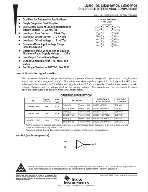
PACKAGING INFORMATIONOrderable Device Status(1)PackageType PackageDrawingPins PackageQtyEco Plan(2)Lead/Ball Finish MSL Peak Temp(3)LM2901AVQDRG4Q1ACTIVE SOIC D142500Green(RoHS&no Sb/Br)CU NIPDAU Level-1-260C-UNLIMLM2901AVQDRQ1ACTIVE SOIC D142500Pb-Free(RoHS)CU NIPDAU Level-2-250C-1YEAR/Level-1-235C-UNLIMLM2901AVQPWRG4Q1ACTIVE TSSOP PW142000Green(RoHS&no Sb/Br)CU NIPDAU Level-1-260C-UNLIMLM2901AVQPWRQ1ACTIVE TSSOP PW142000Pb-Free(RoHS)CU NIPDAU Level-1-250C-UNLIMLM2901QDRG4Q1ACTIVE SOIC D142500Green(RoHS&no Sb/Br)CU NIPDAU Level-1-260C-UNLIMLM2901QDRQ1ACTIVE SOIC D142500Pb-Free(RoHS)CU NIPDAU Level-2-250C-1YEAR/Level-1-235C-UNLIMLM2901QPWRG4Q1ACTIVE TSSOP PW142000Green(RoHS&no Sb/Br)CU NIPDAU Level-1-260C-UNLIM LM2901QPWRQ1ACTIVE TSSOP PW142000TBD CU NIPDAU Level-1-250C-UNLIM LM2901VQDRG4Q1ACTIVE SOIC D142500Green(RoHS&no Sb/Br)CU NIPDAU Level-1-260C-UNLIMLM2901VQDRQ1ACTIVE SOIC D142500Pb-Free(RoHS)CU NIPDAU Level-2-250C-1YEAR/Level-1-235C-UNLIMLM2901VQPWRG4Q1ACTIVE TSSOP PW142000Green(RoHS&no Sb/Br)CU NIPDAU Level-1-260C-UNLIM LM2901VQPWRQ1ACTIVE TSSOP PW142000TBD CU NIPDAU Level-1-250C-UNLIM (1)The marketing status values are defined as follows:ACTIVE:Product device recommended for new designs.LIFEBUY:TI has announced that the device will be discontinued,and a lifetime-buy period is in effect.NRND:Not recommended for new designs.Device is in production to support existing customers,but TI does not recommend using this part in a new design.PREVIEW:Device has been announced but is not in production.Samples may or may not be available.OBSOLETE:TI has discontinued the production of the device.(2)Eco Plan-The planned eco-friendly classification:Pb-Free(RoHS),Pb-Free(RoHS Exempt),or Green(RoHS&no Sb/Br)-please check /productcontent for the latest availability information and additional product content details.TBD:The Pb-Free/Green conversion plan has not been defined.Pb-Free(RoHS):TI's terms"Lead-Free"or"Pb-Free"mean semiconductor products that are compatible with the current RoHS requirements for all6substances,including the requirement that lead not exceed0.1%by weight in homogeneous materials.Where designed to be soldered at high temperatures,TI Pb-Free products are suitable for use in specified lead-free processes.Pb-Free(RoHS Exempt):This component has a RoHS exemption for either1)lead-based flip-chip solder bumps used between the die and package,or2)lead-based die adhesive used between the die and leadframe.The component is otherwise considered Pb-Free(RoHS compatible)as defined above.Green(RoHS&no Sb/Br):TI defines"Green"to mean Pb-Free(RoHS compatible),and free of Bromine(Br)and Antimony(Sb)based flame retardants(Br or Sb do not exceed0.1%by weight in homogeneous material)(3)MSL,Peak Temp.--The Moisture Sensitivity Level rating according to the JEDEC industry standard classifications,and peak solder temperature.Important Information and Disclaimer:The information provided on this page represents TI's knowledge and belief as of the date that it is provided.TI bases its knowledge and belief on information provided by third parties,and makes no representation or warranty as to the accuracy of such information.Efforts are underway to better integrate information from third parties.TI has taken and continues to take reasonable steps to provide representative and accurate information but may not have conducted destructive testing or chemical analysis on incoming materials and chemicals.TI and TI suppliers consider certain information to be proprietary,and thus CAS numbers and other limited information may not be available for release.In no event shall TI's liability arising out of such information exceed the total purchase price of the TI part(s)at issue in this document sold by TIto Customer on an annual basis.OTHER QUALIFIED VERSIONS OF LM2901-Q1,LM2901AV-Q1,LM2901V-Q1:•Catalog:LM2901,LM2901AV,LM2901VNOTE:Qualified Version Definitions:•Catalog-TI's standard catalog productIMPORTANT NOTICETexas Instruments Incorporated and its subsidiaries(TI)reserve the right to make corrections,modifications,enhancements,improvements, and other changes to its products and services at any time and to discontinue any product or service without notice.Customers should obtain the latest relevant information before placing orders and should verify that such information is current and complete.All products are sold subject to TI’s terms and conditions of sale supplied at the time of order acknowledgment.TI warrants performance of its hardware products to the specifications applicable at the time of sale in accordance with TI’s standard warranty.Testing and other quality control techniques are used to the extent TI deems necessary to support this warranty.Except where mandated by government requirements,testing of all parameters of each product is not necessarily performed.TI assumes no liability for applications assistance or customer product design.Customers are responsible for their products and applications using TI components.To minimize the risks associated with customer products and applications,customers should provide adequate design and operating safeguards.TI does not warrant or represent that any license,either express or implied,is granted under any TI patent right,copyright,mask work right, or other TI intellectual property right relating to any combination,machine,or process in which TI products or services are rmation published by TI regarding third-party products or services does not constitute a license from TI to use such products or services or a warranty or endorsement e of such information may require a license from a third party under the patents or other intellectual property of the third party,or a license from TI under the patents or other intellectual property of TI.Reproduction of TI information in TI data books or data sheets is permissible only if reproduction is without alteration and is accompanied by all associated warranties,conditions,limitations,and notices.Reproduction of this information with alteration is an unfair and deceptive business practice.TI is not responsible or liable for such altered rmation of third parties may be subject to additional restrictions.Resale of TI products or services with statements different from or beyond the parameters stated by TI for that product or service voids all express and any implied warranties for the associated TI product or service and is an unfair and deceptive business practice.TI is not responsible or liable for any such statements.TI products are not authorized for use in safety-critical applications(such as life support)where a failure of the TI product would reasonably be expected to cause severe personal injury or death,unless officers of the parties have executed an agreement specifically governing such use.Buyers represent that they have all necessary expertise in the safety and regulatory ramifications of their applications,and acknowledge and agree that they are solely responsible for all legal,regulatory and safety-related requirements concerning their products and any use of TI products in such safety-critical applications,notwithstanding any applications-related information or support that may be provided by TI.Further,Buyers must fully indemnify TI and its representatives against any damages arising out of the use of TI products in such safety-critical applications.TI products are neither designed nor intended for use in military/aerospace applications or environments unless the TI products are specifically designated by TI as military-grade or"enhanced plastic."Only products designated by TI as military-grade meet military specifications.Buyers acknowledge and agree that any such use of TI products which TI has not designated as military-grade is solely at the Buyer's risk,and that they are solely responsible for compliance with all legal and regulatory requirements in connection with such use. TI products are neither designed nor intended for use in automotive applications or environments unless the specific TI products are designated by TI as compliant with ISO/TS16949requirements.Buyers acknowledge and agree that,if they use any non-designated products in automotive applications,TI will not be responsible for any failure to meet such requirements.Following are URLs where you can obtain information on other Texas Instruments products and application solutions:Products ApplicationsAmplifiers AudioData Converters AutomotiveDSP BroadbandClocks and Timers Digital ControlInterface MedicalLogic MilitaryPower Mgmt Optical NetworkingMicrocontrollers SecurityRFID TelephonyRF/IF and ZigBee®Solutions Video&ImagingWirelessMailing Address:Texas Instruments,Post Office Box655303,Dallas,Texas75265Copyright©2008,Texas Instruments Incorporated。
LM2902数据手册_引脚图_参数
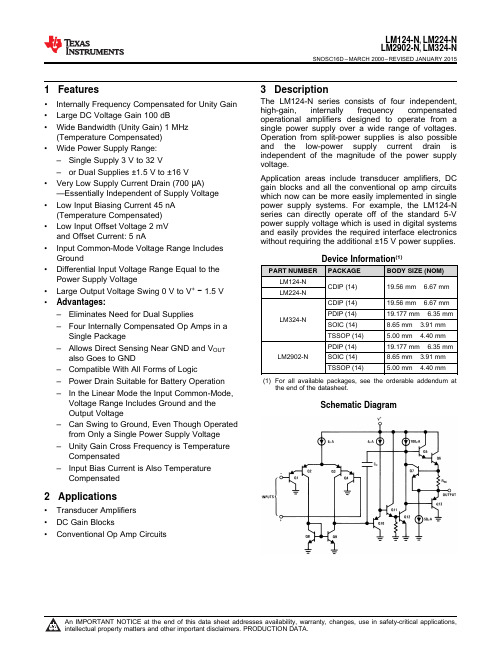
19.177 mm × 6.35 mm 8.65 mm × 3.91 mm
TSSOP (14)
5.00 mm × 4.40 mm
PDIP (14)
19.177 mm × 6.35 mm
LM2902-N
SOIC (14)
8.65 mm × 3.91 mm
TSSOP (14)
5.00 mm × 4.40 mm
(Temperature Compensated) • Wide Power Supply Range:
– Single Supply 3 V to 32 V – or Dual Supplies ±1.5 V to ±16 V • Very Low Supply Current Drain (700 μA) —Essentially Independent of Supply Voltage • Low Input Biasing Current 45 nA (Temperature Compensated) • Low Input Offset Voltage 2 mV and Offset Current: 5 nA • Input Common-Mode Voltage Range Includes Ground • Differential Input Voltage Range Equal to the Power Supply Voltage • Large Output Voltage Swing 0 V to V+ − 1.5 V • Advantages: – Eliminates Need for Dual Supplies – Four Internally Compensated Op Amps in a
Single Package – Allows Direct Sensing Near GND and VOUT
MIX2902_Prilimineary_datasheet_V1.2

180
Temperature
VDD=5.0V
40
MAX
6.0
10
Boost Module Electrical Characteristics
Symbol
Fsw Vfb Ilim ISDB
IQB
Parameter
Boost Frequency Boost feedback
Voltage Boost input current limit
Symbol
Parameter
Test Conditions
MIN TYP
AVDD
Supply Voltage
3.0
-
THD+N=10%,f=1KHZ,RL=4 Ω
PVDD=7.2V
6.3
PO
Output Power
PVDD=6.0V
4
PVDD=7.2V
5.5
THD+N=1%,f=1KHZ,RL=4 Ω
PSRR
AVDD=3.6V±200mVp-p
f=1KHz
60
Rejection
SNR
Signal-to-Noise Ratio
AVDD=3.6V, PVDD=7.2V,
f=1KHz
85
A-weighting
100
Vn
Output Noise
AVDD=3.6V,Input floating with
No
(AVDD =3.6V,PVDD=7.2V,Gain=20dB, RL =4Ω, T =25°C, unless otherwise noted.)
THD+N vs Output Power 20
PCM2902中文资料

D Single Power Supply: 5 V TYP (VBUS) D Stereo ADC
− Analog Performance at VBUS = 5 V − THD+N = 0.01% − SNR = 89 dB − Dynamic Range = 89 dB − Decimation Digital Filter − Pass-Band Ripple = ±0.05 dB − Stop-Band Attenuation = –65 dB − Single-Ended Voltage Input − Antialiasing Filter Included − Digital LCF Included
APPLICATIONS D USB Audio Speaker D USB Headset D USB Monitor D USB Audio Interface Box DESCRIPTION
The PCM2900/2902 is Texas Instruments single-chip USB stereo audio codec with USB-compliant full-speed protocol controller and S/PDIF (only PCM2902). The USB protocol controller works with no software code, but the USB descriptors can be modified in some areas (e.g., vendor ID/product ID). The PCM2900/2902 employs SpAct architecture, TI’s unique system that recovers the audio clock from USB packet data. On-chip analog PLLs with SpAct enable playback and record with low clock jitter and with independent playback and record sampling rates.
- 1、下载文档前请自行甄别文档内容的完整性,平台不提供额外的编辑、内容补充、找答案等附加服务。
- 2、"仅部分预览"的文档,不可在线预览部分如存在完整性等问题,可反馈申请退款(可完整预览的文档不适用该条件!)。
- 3、如文档侵犯您的权益,请联系客服反馈,我们会尽快为您处理(人工客服工作时间:9:00-18:30)。
PACKAGING INFORMATIONOrderable Device Status (1)Package Type Package DrawingPins Package Qty Eco Plan (2)Lead/Ball Finish MSL Peak Temp (3)LM2902KAVQDRQ1ACTIVE SOIC D 142500Pb-Free (RoHS)CU NIPDAU Level-2-250C-1YEAR/Level-1-235C-UNLIM LM2902KAVQPWRQ1ACTIVE TSSOP PW 142000TBD CU NIPDAU Level-1-250C-UNLIM LM2902KVQDRQ1ACTIVE SOIC D 142500Pb-Free (RoHS)CU NIPDAU Level-2-250C-1YEAR/Level-1-235C-UNLIM LM2902KVQPWRQ1ACTIVE TSSOP PW 142000TBD CU NIPDAU Level-1-250C-UNLIM LM2902QDRQ1ACTIVE SOIC D 142500Pb-Free (RoHS)CU NIPDAU Level-2-250C-1YEAR/Level-1-235C-UNLIM LM2902QPWRQ1ACTIVETSSOPPW142000TBDCU NIPDAULevel-1-250C-UNLIM(1)The marketing status values are defined as follows:ACTIVE:Product device recommended for new designs.LIFEBUY:TI has announced that the device will be discontinued,and a lifetime-buy period is in effect.NRND:Not recommended for new designs.Device is in production to support existing customers,but TI does not recommend using this part in a new design.PREVIEW:Device has been announced but is not in production.Samples may or may not be available.OBSOLETE:TI has discontinued the production of the device.(2)Eco Plan -The planned eco-friendly classification:Pb-Free (RoHS),Pb-Free (RoHS Exempt),or Green (RoHS &no Sb/Br)-please check /productcontent for the latest availability information and additional product content details.TBD:The Pb-Free/Green conversion plan has not been defined.Pb-Free (RoHS):TI's terms "Lead-Free"or "Pb-Free"mean semiconductor products that are compatible with the current RoHS requirements for all 6substances,including the requirement that lead not exceed 0.1%by weight in homogeneous materials.Where designed to be soldered at high temperatures,TI Pb-Free products are suitable for use in specified lead-free processes.Pb-Free (RoHS Exempt):This component has a RoHS exemption for either 1)lead-based flip-chip solder bumps used between the die and package,or 2)lead-based die adhesive used between the die and leadframe.The component is otherwise considered Pb-Free (RoHS compatible)as defined above.Green (RoHS &no Sb/Br):TI defines "Green"to mean Pb-Free (RoHS compatible),and free of Bromine (Br)and Antimony (Sb)based flame retardants (Br or Sb do not exceed 0.1%by weight in homogeneous material)(3)MSL,Peak Temp.--The Moisture Sensitivity Level rating according to the JEDEC industry standard classifications,andpeak solder temperature.Important Information and Disclaimer:The information provided on this page represents TI's knowledge and belief as of the date that it is provided.TI bases its knowledge and belief on information provided by third parties,and makes no representation or warranty as to the accuracy of such information.Efforts are underway to better integrate information from third parties.TI has taken and continues to take reasonable steps to provide representative and accurate information but may not have conducted destructive testing or chemical analysis on incoming materials and chemicals.TI and TI suppliers consider certain information to be proprietary,and thus CAS numbers and other limited information may not be available for release.In no event shall TI's liability arising out of such information exceed the total purchase price of the TI part(s)at issue in this document sold by TI to Customer on an annual basis.PACKAGE OPTION ADDENDUM29-May-2007Addendum-Page 1IMPORTANT NOTICETexas Instruments Incorporated and its subsidiaries(TI)reserve the right to make corrections,modifications,enhancements, improvements,and other changes to its products and services at any time and to discontinue any product or service without notice. Customers should obtain the latest relevant information before placing orders and should verify that such information is current and complete.All products are sold subject to TI’s terms and conditions of sale supplied at the time of order acknowledgment.TI warrants performance of its hardware products to the specifications applicable at the time of sale in accordance with TI’s standard warranty.Testing and other quality control techniques are used to the extent TI deems necessary to support this warranty.Except where mandated by government requirements,testing of all parameters of each product is not necessarily performed.TI assumes no liability for applications assistance or customer product design.Customers are responsible for their products and applications using TI components.To minimize the risks associated with customer products and applications,customers should provide adequate design and operating safeguards.TI does not warrant or represent that any license,either express or implied,is granted under any TI patent right,copyright,mask work right,or other TI intellectual property right relating to any combination,machine,or process in which TI products or services are rmation published by TI regarding third-party products or services does not constitute a license from TI to use such products or services or a warranty or endorsement e of such information may require a license from a third party under the patents or other intellectual property of the third party,or a license from TI under the patents or other intellectual property of TI. Reproduction of information in TI data books or data sheets is permissible only if reproduction is without alteration and is accompanied by all associated warranties,conditions,limitations,and notices.Reproduction of this information with alteration is an unfair and deceptive business practice.TI is not responsible or liable for such altered documentation.Resale of TI products or services with statements different from or beyond the parameters stated by TI for that product or service voids all express and any implied warranties for the associated TI product or service and is an unfair and deceptive business practice.TI is not responsible or liable for any such statements.TI products are not authorized for use in safety-critical applications(such as life support)where a failure of the TI product would reasonably be expected to cause severe personal injury or death,unless officers of the parties have executed an agreement specifically governing such use.Buyers represent that they have all necessary expertise in the safety and regulatory ramifications of their applications,and acknowledge and agree that they are solely responsible for all legal,regulatory and safety-related requirements concerning their products and any use of TI products in such safety-critical applications,notwithstanding any applications-related information or support that may be provided by TI.Further,Buyers must fully indemnify TI and its representatives against any damages arising out of the use of TI products in such safety-critical applications.TI products are neither designed nor intended for use in military/aerospace applications or environments unless the TI products are specifically designated by TI as military-grade or"enhanced plastic."Only products designated by TI as military-grade meet military specifications.Buyers acknowledge and agree that any such use of TI products which TI has not designated as military-grade is solely at the Buyer's risk,and that they are solely responsible for compliance with all legal and regulatory requirements in connection with such use.TI products are neither designed nor intended for use in automotive applications or environments unless the specific TI products are designated by TI as compliant with ISO/TS16949requirements.Buyers acknowledge and agree that,if they use anynon-designated products in automotive applications,TI will not be responsible for any failure to meet such requirements. Following are URLs where you can obtain information on other Texas Instruments products and application solutions:Products ApplicationsAmplifiers Audio /audioData Converters Automotive /automotiveDSP Broadband /broadbandInterface Digital Control /digitalcontrolLogic Military /militaryPower Mgmt Optical Networking /opticalnetworkMicrocontrollers Security /securityRFID Telephony /telephonyLow Power /lpw Video&Imaging /videoWirelessWireless /wirelessMailing Address:Texas Instruments,Post Office Box655303,Dallas,Texas75265Copyright©2007,Texas Instruments Incorporated。
