HZ16A3中文资料
FMP3217BA0-GXXX资料
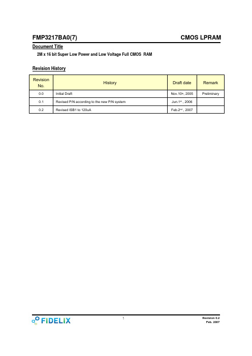
Name VCC VCCQ VSS /UB /LB DNU
Function Core Power I/O Power Ground Upper Byte(I/O9~16) Lower Byte(I/O 1~8) Do Not Use
/CS1 CS2 /OE Control Logic /WE /UB /LB
• Organization : 2M x 16 • Power Supply Voltage : 2.7~3.3V • Dual CS & Page Modes
FMP3217BA0 : Dual CS FMP3217BA7 : Page mode with Dual CS
CMOS LPRAM
2M x 16 bit Super Low Power and Low Voltage Full CMOS RAM
)
Unit Min 2.7 2.25 0 0.8VCCQ -0.22) Max 3.3 2.75 0 VCC+0.21) 0.2VCCQ Min 2.7 1.65 0 0.8VCCQ -0.22) Max 3.3 1.95 0 VCC+0.21) 0.2VCCQ V V V V V
0.2VCCQ
Note : 1. Overshoot : Vcc+1.0V in case of pulse width≤20ns. 2. Undershoot : -1.0V in case of pulse width≤20ns. 3. Overshoot and undershoot are sampled, not 100% tested.
/LB X1) X1) H L
/UB X1) X1) H X1) L H L L H L L
2SA3中文说明书

安 全该电气机械和设备是在工业强电流的条件下使用的。
在操作中,该设备上有些裸露零件带电,同时有些零件能够运动或转动,都是很危险的。
因此,未经许可拆下所需的罩盖,不合理的使用,不正确的操作或不合适的维护,均会造成严重的人身伤害或损坏设备性能。
为了设备的安全,必须保证:——仅允许有资格的人员对这些机械和设备进行作业。
——无论何时,在上述有资格的人员对该机械和设备进行作业时,他们都应备有这些机械和设备的操作说明书或其它产品文件,以便按说明书的要求执行。
——严禁没有资格的人员对该机械和设备进行作业或在其附近进行作业。
目录1 运输及保管 (1)2 概述 (1)2.1 应用 (1)2.2 结构及原理 (1)2.3 手动操作 (3)2.4 电机 (3)2.5 连接及安装 (3)2.6 电气连接 (4)3开关及信号部分的调整 (5)3.1 转矩控制机构DSW(开关S1、S2)调整 (5)3.2 信号齿轮组件调整 (6)3.3 行程控制计数器机构RSW的调整 (7)3.4 行程控制凸轮机构NSW的调整 (8)3.5 电位器POT (9)3.6电子位置发送器ESR (9)3.7机械位置指示器SA (10)3.8投入运行 (10)4维修及保养 (10)4.1检查及校调 (11)4.2润滑材料的检查及加注周期 (11)附录1电子位置发送器的主要参数与调整 (12)1 概述 (12)2 安装连接 (12)3 模式调节 (12)4 调整 (14)附录2连接型式及尺寸 (16)法兰连接尺寸(GB12222)(见附图5和附表1) (16)输出轴尺寸(GB12222)(附图6至附图8,附表2至附表4) (17)可传递转矩和推力的输出轴型式(附图6、附表2) (17)仅传递转矩的输出轴型式(附图7、附图8,附表3、附表4) (17)连接尺寸(JB2920)(附图9、附表5) (19)2SA3电动执行机构为一种机电装置,在运输、保管、安装、调试维修时应严格按照本说明书的各项要求进行,以避免发生故障及损伤。
变频门机调试说明书_松下变频器_中文

目录第一、变频器接线 (1)第二、变频器调试 (3)第三、功能参数表 (11)第四、故障监控表 (15)日期:2007-05-18版本:第A版第二部分变频器调试修改:第0次第二、变频器调试操作说明:为使门机完成自学习及正常运行,需适当改变一些参数值。
修改参数的基本操作如下:按“MODE”键会循环出现Fr,dr,n及P菜单,d菜单在P菜单后。
进入P菜单后,按“▲”键,P菜单的参数项增加,达到P79后再按“▲”键就进入d菜单,按“▼”键可返回P菜单。
进入指定菜单项,按“SET”键,再根据情况按“▲”或“▼”键,可改变该参数值,改完后按“SET”键参数值就修改完毕并返回该参数的下一项。
注:P08和P09的值不能在线修改,须按下“STOP”键后方可修改。
一:磁开关控制方式1检查线路,请参考图1-2接线图仔细查看变频器信号是否接错。
2 确认电机正反转:2.1 按“MODE”键出现Fr菜单,设置Fr为3。
2.2 进入P级菜单,设置P08=1,P09=0。
然后按“MODE”键返回原始界面(OOO)。
2.3 先按▲,再按RUN,确认门在开动作;然后按下▼,再按RUN确认门在关动作。
若门不动作或动作太缓慢,需按“STOP”键返回原始界面(OOO),再进入P级菜单把P05的值增大到20左右(力矩提升)。
若门运行方向相反,则改变电机U,V,W中的任意两相。
2.4 确认电机转向正确后按“STOP”键,返回原始界面(OOO)。
3 模式设定:请参考表2-1,表2-2。
4 进入P级菜单,设置P43的值为3(有编码器)、27(无编码器)。
5 运行:设置P09的值为5,然后按“MODE”键返回原始界面(OOO)。
先按▲,再按RUN或先按▼,再按RUN;门机将自动检测磁开关的位置,并自动运行。
6 运行曲线调整:参数设置完毕后,门机在开关门时已经有了一定的运行曲线,如果运行曲线不够平滑,则可以对运行曲线进行微调。
开门调节曲线见图2-1,关门调节曲线见图2-2,曲线调节方法见图2-5。
HZ6C2中文资料

HZ SeriesSilicon Epitaxial Planar Zener Diode for Stabilized Power SupplyADE-208-117B(Z)Rev. 2Nov. 1999 Features•Low leakage, low zener impedance and maximum power dissipation of 500 mW are ideally suited for stabilized power supply, etc.•Wide spectrum from 1.6V through 38V of zener voltage provide flexible application.Ordering InformationType No.Mark Package CodeHZ Series Type No.DO-35OutlineHZ SeriesRev.2, Nov. 1999, page 2 of 8Absolute Maximum Ratings(Ta = 25°C)ItemSymbol Value Unit Power dissipation Pd 500mW Junction temperature Tj 175°C Storage temperatureTstg-55 to +175°CElectrical Characteristics(Ta = 25°C)Zener Voltage Reverese CurrentDynamic Resistance V Z (V)*1TestConditionI R (µA)TestCondition r d (Ω)TestCondition Type Grade Min Max I Z (mA)Max V R (V)Max I Z (mA)HZ2A1 1.6 1.85250.51005A2 1.7 1.9A3 1.8 2.0B1 1.9 2.1550.51005B2 2.0 2.2B3 2.1 2.3C1 2.2 2.4C2 2.3 2.5C32.4 2.6HZ3A1 2.5 2.7550.51005A2 2.6 2.8A3 2.7 2.9B1 2.8 3.0B2 2.9 3.1B3 3.0 3.2C1 3.1 3.3C2 3.2 3.4C33.3 3.5HZ4A1 3.4 3.655 1.01005A2 3.5 3.7A33.63.8Note:1.Tested with DC.HZ SeriesRev.2, Nov. 1999, page 3 of 8Zener Voltage Reverese CurrentDynamic Resistance V Z (V)*1TestConditionI R (µA)TestCondition r d (Ω)TestCondition Type Grade Min Max I Z (mA)Max V R (V)Max I Z (mA)HZ4B1 3.7 3.9551.01005B2 3.8 4.0B3 3.9 4.1C1 4.0 4.2C2 4.1 4.3C34.2 4.4HZ5A1 4.3 4.555 1.51005A2 4.4 4.6A3 4.5 4.7B1 4.6 4.8B2 4.7 4.9B3 4.8 5.0C1 4.9 5.1C2 5.0 5.2C35.1 5.3HZ6A1 5.2 5.555 2.0405A2 5.3 5.6A3 5.4 5.7B1 5.5 5.8B2 5.6 5.9B3 5.7 6.0C1 5.8 6.1C2 6.0 6.3C36.1 6.4HZ7A1 6.3 6.651 3.5155A2 6.4 6.7A3 6.6 6.9B1 6.77.0B2 6.97.2B37.07.3Note:1.Tested with DC.HZ SeriesRev.2, Nov. 1999, page 4 of 8Zener Voltage Reverese CurrentDynamic Resistance V Z (V)*1TestConditionI R (µA)TestCondition r d (Ω)TestCondition Type Grade Min Max I Z (mA)Max V R (V)Max I Z (mA)HZ7C17.27.6513.5155C27.37.7C37.57.9HZ9A17.78.151 5.0205A27.98.3A38.18.5B18.38.7B28.58.9B38.79.1C18.99.3C29.19.5C39.39.7HZ11A19.59.9517.5255A29.710.1A39.910.3B110.210.6B210.410.8B310.711.1C110.911.3C211.111.6C311.411.9HZ12A111.612.1519.5355A211.912.4A312.212.7B112.412.9B212.613.1B312.913.4C113.213.7C213.514.0C313.814.3Note:1.Tested with DC.HZ SeriesRev.2, Nov. 1999, page 5 of 8Zener Voltage Reverese CurrentDynamic Resistance V Z (V)*1TestConditionI R (µA)TestCondition r d (Ω)TestCondition Type Grade Min Max I Z (mA)Max V R (V)Max I Z (mA)HZ15114.114.75111.0405214.515.1314.915.5HZ16115.315.95112.0455215.716.5316.317.1HZ18116.917.75113.0555217.518.3318.119.0HZ20118.819.72115.0602219.520.4320.221.1HZ22120.921.92117.0652221.622.6322.323.3HZ24122.924.02119.0702223.624.7324.325.5HZ27125.226.62121.0802226.227.6327.228.6HZ30128.229.62123.01002229.230.6330.231.6HZ33131.232.62125.01202232.233.6333.234.6HZ36134.235.72127.01402235.336.8336.438.0Note: 1.Tested with DC.Note:2.Type No. is as follows; HZ2B1, HZ2B2, HZ36-3.HZ SeriesMain CharacteristicRev.2, Nov. 1999, page 6 of 8HZ Series Package DimensionsRev.2, Nov. 1999, page 7 of 8HZ SeriesRev.2, Nov. 1999, page 8 of 8Disclaimer1.Hitachi neither warrants nor grants licenses of any rights of Hitachi’s or any third party’s patent,copyright, trademark, or other intellectual property rights for information contained in this document.Hitachi bears no responsibility for problems that may arise with third party’s rights, including intellectual property rights, in connection with use of the information contained in this document.2.Products and product specifications may be subject to change without notice. Confirm that you have received the latest product standards or specifications before final design, purchase or use.3.Hitachi makes every attempt to ensure that its products are of high quality and reliability. However,contact Hitachi’s sales office before using the product in an application that demands especially high quality and reliability or where its failure or malfunction may directly threaten human life or cause risk of bodily injury, such as aerospace, aeronautics, nuclear power, combustion control, transportation,traffic, safety equipment or medical equipment for life support.4.Design your application so that the product is used within the ranges guaranteed by Hitachi particularly for maximum rating, operating supply voltage range, heat radiation characteristics, installationconditions and other characteristics. Hitachi bears no responsibility for failure or damage when used beyond the guaranteed ranges. Even within the guaranteed ranges, consider normally foreseeable failure rates or failure modes in semiconductor devices and employ systemic measures such as fail-safes, so that the equipment incorporating Hitachi product does not cause bodily injury, fire or other consequential damage due to operation of the Hitachi product.5.This product is not designed to be radiation resistant.6.No one is permitted to reproduce or duplicate, in any form, the whole or part of this document without written approval from Hitachi.7.Contact Hitachi’s sales office for any questions regarding this document or Hitachi semiconductor products.Sales OfficesHitachi, Ltd.Semiconductor & Integrated CircuitsNippon Bldg., 2-6-2, Ohte-machi, Chiyoda-ku, Tokyo 100-0004, Japan Tel: (03) 3270-2111 Fax: (03) 3270-5109Copyright © Hitachi, Ltd., 2001. All rights reserved. Printed in Japan.Hitachi Asia Ltd. Hitachi Tower16 Collyer Quay #20-00 Singapore 049318Tel : <65>-538-6533/538-8577 Fax : <65>-538-6933/538-3877URL : .sg URLNorthAmerica : /Europe : /hel/ecg Asia : Japan : http://www.hitachi.co.jp/Sicd/indx.htmHitachi Asia Ltd.(Taipei Branch Office)4/F, No. 167, Tun Hwa North Road Hung-Kuo Building Taipei (105), Taiwan Tel : <886>-(2)-2718-3666 Fax : <886>-(2)-2718-8180 Telex : 23222 HAS-TPURL : Hitachi Asia (Hong Kong) Ltd.Group III (Electronic Components) 7/F., North TowerWorld Finance Centre,Harbour City, Canton Road Tsim Sha Tsui, Kowloon Hong KongTel : <852>-(2)-735-9218 Fax : <852>-(2)-730-0281URL : Hitachi Europe GmbHElectronic Components Group Dornacher Straße 3D-85622 Feldkirchen, Munich GermanyTel: <49> (89) 9 9180-0Fax: <49> (89) 9 29 30 00Hitachi Europe Ltd.Electronic Components Group Whitebrook ParkLower Cookham Road MaidenheadBerkshire SL6 8YA, United Kingdom Tel: <44> (1628) 585000Fax: <44> (1628) 585200Hitachi Semiconductor (America) Inc.179 East Tasman Drive San Jose,CA 95134 Tel: <1> (408) 433-1990Fax: <1>(408) 433-0223For further information write to:Colophon 4.0。
ht1622命令中文版

禁止时基输出
默认状态
WDTDIS
100
0000-0101-X
C
禁止WDT超时输出
默认状态
TIMER EN
100
0000-0110-X
C
使能时基输出
WDTEN
100
0000-0111-X
C
使能WDT超时输出
TONE OFF
100
0000-1000-X
C
关闭音频输出
默认状态
CLRTIMER
100
0000-1101-X
Name
ID
CommandCode
D/C
Function
默认状态.
READ
110
A5A4A3A2A1A0D0D1D2D3
D
读RAM数据
WRITE
101
A5A4A3A2A1A0D0D1D2D3
D
写数据到RAM
READ-MODIFY- WRITE
101
A5A4A3A2A1A0D0D1D2D3
D
读和写数据到RAM
SYSDIS
100
0000-0000-X
C
关闭系统振荡器和LCD偏压发生器
默认状态
SYSEN
100
0000-0001-X
C
打开系统振荡器
LCD OFF
100
0000-0010-X
C
关闭液晶显示屏
默认状态
LCD ON
100
0000-0011-X
C
打开液晶显示屏
TIMER DIS
100
0000-0100-X
100
101X-0101-X
C
ETSI EN 303 447 V1.1.1中文版【经典】

ETSI EN 303 447 V1.1.1 (2017-09)短程装置(SRD)频率范围为0Hz-148.5kHz的具有感应回路系统的自动割草机涵盖指令2014/53/EU第3.2节基本要求的协调标准1目录知识产权 (4)前言 (4)情态动词术语 (4)简介 (5)1范围 (6)2参考文献 (7)2.1规范性引用文件 (7)2.2参考资料 (7)3定义、符号和缩写 (8)3.1定义 (8)3.2符号 (9)3.3缩写 (9)4技术要求规范 (10)4.1环境条件 (10)4.2概述 (10)4.2.1期望的性能指标 (10)4.2.2RMI功能模式 (10)4.2.2.1概述 (10)4.2.2.2操作模式 (10)4.2.2.3安全模式 (11)4.2.3测试设备介绍 (11)4.3发射机一致性要求 (11)4.3.1工作频率范围(OFR) (11)4.3.1.1适用范围 (11)4.3.1.2说明 (11)4.3.1.3限制 (12)4.3.1.4一致性 (12)4.3.2发射机磁场(H-field)要求 (12)4.3.2.1适用范围 (12)4.3.2.2说明 (12)4.3.2.3限制 (12)4.3.2.4一致性 (13)4.3.3发射机杂散发射 (13)4.3.3.1适用范围 (13)4.3.3.2说明 (13)4.3.3.3限制 (14)4.3.3.4一致性 (14)4.3.4发射机带外(OOB)发射 (14)4.3.4.1适用性 (14)4.3.4.2描述 (14)4.3.4.3限制 (15)24.3.4.4一致性 (15)4.4接收机一致性要求 (15)4.4.1介绍 (15)4.4.2接收机无用发射 (15)4.4.3接收机阻塞(干扰) (15)4.4.3.1适用性 (15)4.4.3.2说明 (15)4.4.3.3限制 (15)4.4.3.4一致性 (16)5符合技术要求的试验 (17)5.1试验环境条件 (17)5.2试验一般条件 (17)5.2.1产品介绍 (17)5.3正常和极端的测试条件 (17)5.4人造天线 (17)5.5辐射测量的试验场地和总体布置 (17)5.6测量接收机 (17)5.7测量结果的不确定度 (18)5.8测量结果的解释 (18)6发射机和接收机的一致性测量方法 (19)6.1概述 (19)6.2发射机一致性方法 (19)6.2.1工作频率范围(OFR) (19)6.2.2磁场 (20)6.2.3发射机无用发射(杂散和带外(OOB)发射) (20)6.3接收机一致性方法 (21)6.3.1接收机杂散发射 (21)6.3.2接收机阻塞干扰 (21)附录A(资料性)本文件与2014/53/EU指令基本要求的关系 (24)附录B (规范性): 测试场地和程序 (25)B.1 设置1:试验园的磁场测量 (25)B.2设置2:使用人造天线测量载波电流 (25)B.2.1概述 (25)B.2.2差模测量 (26)B.2.3共模测量 (26)B.3使用消声室或开放区域测试场所进行辐射测量 (26)附件C(规范性):人造天线,用于30 MHz以下的传导测量 (27)附件D (资料性): 变更历史 (29)历史 (29)3知识产权必要专利本文件所必需或潜在必需的知识产权可能已向ETSI申报。
MS中文数据手册

晶振,XIN,XOUT
注释:1.晶体两端都需要连接电容,电容值由晶体制造商规定。
2.仅当使用一个外部逻辑水平时钟源时适用,使用晶体或谐振器时不适用。
注释:x为P2口的位标识符6到7,在元件上没有与这两位对应的外部引脚
注释:将P2口未连接的两位6和7用作中断标志是一种良好的应用方法,除了软件其他信号不会影响到这两个中断标志,从而它们被用作软件中断。
JTAG熔丝检查模式
上电复位(POR)后第一次使用JTAG口,在TEST端有熔丝的MSP430设备有一个熔丝检查模式,可以检测熔丝的通断。该模式有效时,如果熔丝没烧断,将有一个熔丝检查电流Itf(电压3V时1mA,电压5V时2.5mA)从TEST引脚流到地,必须防止意外激活熔丝检查模式,以免增加系统功耗。
可选电阻,独立可编程(参阅注释1)
注释1:在标准OTP或者EPROM设备MSP430P112或MSP430E112中,用于上拉或下拉的可选电阻R optx 是不可编程的。
从低电压模式唤醒响应时间(LPMx)
注释1:这个参数是保持程序存储器(RAM)中数据不丢失所需的最小电压,在这个电压下,程序不能执行。
2.数字端口引脚的泄露电流要单个测量。端口引脚必须选择为输入并且没有选择上拉或下拉电阻。
输出 P2x,Tax
输出P1口和P2口
注释:1.对于所有输出组合,最大总电流I OH(max)和I OL(max)不能超过±12mA,以便输出电压满足输出电压下降标准。
2.对于所有输出组合,最大总电流I OH(max)和I OL(max)不能超过±36mA,以便输出电压满足输出电压下降标准。
HZ6B1中文资料

HZ SeriesSilicon Epitaxial Planar Zener Diode for Stabilized Power SupplyADE-208-117B(Z)Rev. 2Nov. 1999 Features•Low leakage, low zener impedance and maximum power dissipation of 500 mW are ideally suited for stabilized power supply, etc.•Wide spectrum from 1.6V through 38V of zener voltage provide flexible application.Ordering InformationType No.Mark Package CodeHZ Series Type No.DO-35OutlineHZ SeriesRev.2, Nov. 1999, page 2 of 8Absolute Maximum Ratings(Ta = 25°C)ItemSymbol Value Unit Power dissipation Pd 500mW Junction temperature Tj 175°C Storage temperatureTstg-55 to +175°CElectrical Characteristics(Ta = 25°C)Zener Voltage Reverese CurrentDynamic Resistance V Z (V)*1TestConditionI R (µA)TestCondition r d (Ω)TestCondition Type Grade Min Max I Z (mA)Max V R (V)Max I Z (mA)HZ2A1 1.6 1.85250.51005A2 1.7 1.9A3 1.8 2.0B1 1.9 2.1550.51005B2 2.0 2.2B3 2.1 2.3C1 2.2 2.4C2 2.3 2.5C32.4 2.6HZ3A1 2.5 2.7550.51005A2 2.6 2.8A3 2.7 2.9B1 2.8 3.0B2 2.9 3.1B3 3.0 3.2C1 3.1 3.3C2 3.2 3.4C33.3 3.5HZ4A1 3.4 3.655 1.01005A2 3.5 3.7A33.63.8Note:1.Tested with DC.HZ SeriesRev.2, Nov. 1999, page 3 of 8Zener Voltage Reverese CurrentDynamic Resistance V Z (V)*1TestConditionI R (µA)TestCondition r d (Ω)TestCondition Type Grade Min Max I Z (mA)Max V R (V)Max I Z (mA)HZ4B1 3.7 3.9551.01005B2 3.8 4.0B3 3.9 4.1C1 4.0 4.2C2 4.1 4.3C34.2 4.4HZ5A1 4.3 4.555 1.51005A2 4.4 4.6A3 4.5 4.7B1 4.6 4.8B2 4.7 4.9B3 4.8 5.0C1 4.9 5.1C2 5.0 5.2C35.1 5.3HZ6A1 5.2 5.555 2.0405A2 5.3 5.6A3 5.4 5.7B1 5.5 5.8B2 5.6 5.9B3 5.7 6.0C1 5.8 6.1C2 6.0 6.3C36.1 6.4HZ7A1 6.3 6.651 3.5155A2 6.4 6.7A3 6.6 6.9B1 6.77.0B2 6.97.2B37.07.3Note:1.Tested with DC.HZ SeriesRev.2, Nov. 1999, page 4 of 8Zener Voltage Reverese CurrentDynamic Resistance V Z (V)*1TestConditionI R (µA)TestCondition r d (Ω)TestCondition Type Grade Min Max I Z (mA)Max V R (V)Max I Z (mA)HZ7C17.27.6513.5155C27.37.7C37.57.9HZ9A17.78.151 5.0205A27.98.3A38.18.5B18.38.7B28.58.9B38.79.1C18.99.3C29.19.5C39.39.7HZ11A19.59.9517.5255A29.710.1A39.910.3B110.210.6B210.410.8B310.711.1C110.911.3C211.111.6C311.411.9HZ12A111.612.1519.5355A211.912.4A312.212.7B112.412.9B212.613.1B312.913.4C113.213.7C213.514.0C313.814.3Note:1.Tested with DC.HZ SeriesRev.2, Nov. 1999, page 5 of 8Zener Voltage Reverese CurrentDynamic Resistance V Z (V)*1TestConditionI R (µA)TestCondition r d (Ω)TestCondition Type Grade Min Max I Z (mA)Max V R (V)Max I Z (mA)HZ15114.114.75111.0405214.515.1314.915.5HZ16115.315.95112.0455215.716.5316.317.1HZ18116.917.75113.0555217.518.3318.119.0HZ20118.819.72115.0602219.520.4320.221.1HZ22120.921.92117.0652221.622.6322.323.3HZ24122.924.02119.0702223.624.7324.325.5HZ27125.226.62121.0802226.227.6327.228.6HZ30128.229.62123.01002229.230.6330.231.6HZ33131.232.62125.01202232.233.6333.234.6HZ36134.235.72127.01402235.336.8336.438.0Note: 1.Tested with DC.Note:2.Type No. is as follows; HZ2B1, HZ2B2, HZ36-3.HZ SeriesMain CharacteristicRev.2, Nov. 1999, page 6 of 8HZ Series Package DimensionsRev.2, Nov. 1999, page 7 of 8HZ SeriesRev.2, Nov. 1999, page 8 of 8Disclaimer1.Hitachi neither warrants nor grants licenses of any rights of Hitachi’s or any third party’s patent,copyright, trademark, or other intellectual property rights for information contained in this document.Hitachi bears no responsibility for problems that may arise with third party’s rights, including intellectual property rights, in connection with use of the information contained in this document.2.Products and product specifications may be subject to change without notice. Confirm that you have received the latest product standards or specifications before final design, purchase or use.3.Hitachi makes every attempt to ensure that its products are of high quality and reliability. However,contact Hitachi’s sales office before using the product in an application that demands especially high quality and reliability or where its failure or malfunction may directly threaten human life or cause risk of bodily injury, such as aerospace, aeronautics, nuclear power, combustion control, transportation,traffic, safety equipment or medical equipment for life support.4.Design your application so that the product is used within the ranges guaranteed by Hitachi particularly for maximum rating, operating supply voltage range, heat radiation characteristics, installationconditions and other characteristics. Hitachi bears no responsibility for failure or damage when used beyond the guaranteed ranges. Even within the guaranteed ranges, consider normally foreseeable failure rates or failure modes in semiconductor devices and employ systemic measures such as fail-safes, so that the equipment incorporating Hitachi product does not cause bodily injury, fire or other consequential damage due to operation of the Hitachi product.5.This product is not designed to be radiation resistant.6.No one is permitted to reproduce or duplicate, in any form, the whole or part of this document without written approval from Hitachi.7.Contact Hitachi’s sales office for any questions regarding this document or Hitachi semiconductor products.Sales OfficesHitachi, Ltd.Semiconductor & Integrated CircuitsNippon Bldg., 2-6-2, Ohte-machi, Chiyoda-ku, Tokyo 100-0004, Japan Tel: (03) 3270-2111 Fax: (03) 3270-5109Copyright © Hitachi, Ltd., 2001. All rights reserved. Printed in Japan.Hitachi Asia Ltd. Hitachi Tower16 Collyer Quay #20-00 Singapore 049318Tel : <65>-538-6533/538-8577 Fax : <65>-538-6933/538-3877URL : .sg URLNorthAmerica : /Europe : /hel/ecg Asia : Japan : http://www.hitachi.co.jp/Sicd/indx.htmHitachi Asia Ltd.(Taipei Branch Office)4/F, No. 167, Tun Hwa North Road Hung-Kuo Building Taipei (105), Taiwan Tel : <886>-(2)-2718-3666 Fax : <886>-(2)-2718-8180 Telex : 23222 HAS-TPURL : Hitachi Asia (Hong Kong) Ltd.Group III (Electronic Components) 7/F., North TowerWorld Finance Centre,Harbour City, Canton Road Tsim Sha Tsui, Kowloon Hong KongTel : <852>-(2)-735-9218 Fax : <852>-(2)-730-0281URL : Hitachi Europe GmbHElectronic Components Group Dornacher Straße 3D-85622 Feldkirchen, Munich GermanyTel: <49> (89) 9 9180-0Fax: <49> (89) 9 29 30 00Hitachi Europe Ltd.Electronic Components Group Whitebrook ParkLower Cookham Road MaidenheadBerkshire SL6 8YA, United Kingdom Tel: <44> (1628) 585000Fax: <44> (1628) 585200Hitachi Semiconductor (America) Inc.179 East Tasman Drive San Jose,CA 95134 Tel: <1> (408) 433-1990Fax: <1>(408) 433-0223For further information write to:Colophon 4.0。
HZ3A3中文资料

HZ SeriesSilicon Epitaxial Planar Zener Diode for Stabilized Power SupplyADE-208-117B(Z)Rev. 2Nov. 1999 Features•Low leakage, low zener impedance and maximum power dissipation of 500 mW are ideally suited for stabilized power supply, etc.•Wide spectrum from 1.6V through 38V of zener voltage provide flexible application.Ordering InformationType No.Mark Package CodeHZ Series Type No.DO-35OutlineHZ SeriesRev.2, Nov. 1999, page 2 of 8Absolute Maximum Ratings(Ta = 25°C)ItemSymbol Value Unit Power dissipation Pd 500mW Junction temperature Tj 175°C Storage temperatureTstg-55 to +175°CElectrical Characteristics(Ta = 25°C)Zener Voltage Reverese CurrentDynamic Resistance V Z (V)*1TestConditionI R (µA)TestCondition r d (Ω)TestCondition Type Grade Min Max I Z (mA)Max V R (V)Max I Z (mA)HZ2A1 1.6 1.85250.51005A2 1.7 1.9A3 1.8 2.0B1 1.9 2.1550.51005B2 2.0 2.2B3 2.1 2.3C1 2.2 2.4C2 2.3 2.5C32.4 2.6HZ3A1 2.5 2.7550.51005A2 2.6 2.8A3 2.7 2.9B1 2.8 3.0B2 2.9 3.1B3 3.0 3.2C1 3.1 3.3C2 3.2 3.4C33.3 3.5HZ4A1 3.4 3.655 1.01005A2 3.5 3.7A33.63.8Note:1.Tested with DC.HZ SeriesRev.2, Nov. 1999, page 3 of 8Zener Voltage Reverese CurrentDynamic Resistance V Z (V)*1TestConditionI R (µA)TestCondition r d (Ω)TestCondition Type Grade Min Max I Z (mA)Max V R (V)Max I Z (mA)HZ4B1 3.7 3.9551.01005B2 3.8 4.0B3 3.9 4.1C1 4.0 4.2C2 4.1 4.3C34.2 4.4HZ5A1 4.3 4.555 1.51005A2 4.4 4.6A3 4.5 4.7B1 4.6 4.8B2 4.7 4.9B3 4.8 5.0C1 4.9 5.1C2 5.0 5.2C35.1 5.3HZ6A1 5.2 5.555 2.0405A2 5.3 5.6A3 5.4 5.7B1 5.5 5.8B2 5.6 5.9B3 5.7 6.0C1 5.8 6.1C2 6.0 6.3C36.1 6.4HZ7A1 6.3 6.651 3.5155A2 6.4 6.7A3 6.6 6.9B1 6.77.0B2 6.97.2B37.07.3Note:1.Tested with DC.HZ SeriesRev.2, Nov. 1999, page 4 of 8Zener Voltage Reverese CurrentDynamic Resistance V Z (V)*1TestConditionI R (µA)TestCondition r d (Ω)TestCondition Type Grade Min Max I Z (mA)Max V R (V)Max I Z (mA)HZ7C17.27.6513.5155C27.37.7C37.57.9HZ9A17.78.151 5.0205A27.98.3A38.18.5B18.38.7B28.58.9B38.79.1C18.99.3C29.19.5C39.39.7HZ11A19.59.9517.5255A29.710.1A39.910.3B110.210.6B210.410.8B310.711.1C110.911.3C211.111.6C311.411.9HZ12A111.612.1519.5355A211.912.4A312.212.7B112.412.9B212.613.1B312.913.4C113.213.7C213.514.0C313.814.3Note:1.Tested with DC.HZ SeriesRev.2, Nov. 1999, page 5 of 8Zener Voltage Reverese CurrentDynamic Resistance V Z (V)*1TestConditionI R (µA)TestCondition r d (Ω)TestCondition Type Grade Min Max I Z (mA)Max V R (V)Max I Z (mA)HZ15114.114.75111.0405214.515.1314.915.5HZ16115.315.95112.0455215.716.5316.317.1HZ18116.917.75113.0555217.518.3318.119.0HZ20118.819.72115.0602219.520.4320.221.1HZ22120.921.92117.0652221.622.6322.323.3HZ24122.924.02119.0702223.624.7324.325.5HZ27125.226.62121.0802226.227.6327.228.6HZ30128.229.62123.01002229.230.6330.231.6HZ33131.232.62125.01202232.233.6333.234.6HZ36134.235.72127.01402235.336.8336.438.0Note: 1.Tested with DC.Note:2.Type No. is as follows; HZ2B1, HZ2B2, HZ36-3.HZ SeriesMain CharacteristicRev.2, Nov. 1999, page 6 of 8HZ Series Package DimensionsRev.2, Nov. 1999, page 7 of 8HZ SeriesRev.2, Nov. 1999, page 8 of 8Disclaimer1.Hitachi neither warrants nor grants licenses of any rights of Hitachi’s or any third party’s patent,copyright, trademark, or other intellectual property rights for information contained in this document.Hitachi bears no responsibility for problems that may arise with third party’s rights, including intellectual property rights, in connection with use of the information contained in this document.2.Products and product specifications may be subject to change without notice. Confirm that you have received the latest product standards or specifications before final design, purchase or use.3.Hitachi makes every attempt to ensure that its products are of high quality and reliability. However,contact Hitachi’s sales office before using the product in an application that demands especially high quality and reliability or where its failure or malfunction may directly threaten human life or cause risk of bodily injury, such as aerospace, aeronautics, nuclear power, combustion control, transportation,traffic, safety equipment or medical equipment for life support.4.Design your application so that the product is used within the ranges guaranteed by Hitachi particularly for maximum rating, operating supply voltage range, heat radiation characteristics, installationconditions and other characteristics. Hitachi bears no responsibility for failure or damage when used beyond the guaranteed ranges. Even within the guaranteed ranges, consider normally foreseeable failure rates or failure modes in semiconductor devices and employ systemic measures such as fail-safes, so that the equipment incorporating Hitachi product does not cause bodily injury, fire or other consequential damage due to operation of the Hitachi product.5.This product is not designed to be radiation resistant.6.No one is permitted to reproduce or duplicate, in any form, the whole or part of this document without written approval from Hitachi.7.Contact Hitachi’s sales office for any questions regarding this document or Hitachi semiconductor products.Sales OfficesHitachi, Ltd.Semiconductor & Integrated CircuitsNippon Bldg., 2-6-2, Ohte-machi, Chiyoda-ku, Tokyo 100-0004, Japan Tel: (03) 3270-2111 Fax: (03) 3270-5109Copyright © Hitachi, Ltd., 2001. All rights reserved. Printed in Japan.Hitachi Asia Ltd. Hitachi Tower16 Collyer Quay #20-00 Singapore 049318Tel : <65>-538-6533/538-8577 Fax : <65>-538-6933/538-3877URL : .sg URLNorthAmerica : /Europe : /hel/ecg Asia : Japan : http://www.hitachi.co.jp/Sicd/indx.htmHitachi Asia Ltd.(Taipei Branch Office)4/F, No. 167, Tun Hwa North Road Hung-Kuo Building Taipei (105), Taiwan Tel : <886>-(2)-2718-3666 Fax : <886>-(2)-2718-8180 Telex : 23222 HAS-TPURL : Hitachi Asia (Hong Kong) Ltd.Group III (Electronic Components) 7/F., North TowerWorld Finance Centre,Harbour City, Canton Road Tsim Sha Tsui, Kowloon Hong KongTel : <852>-(2)-735-9218 Fax : <852>-(2)-730-0281URL : Hitachi Europe GmbHElectronic Components Group Dornacher Straße 3D-85622 Feldkirchen, Munich GermanyTel: <49> (89) 9 9180-0Fax: <49> (89) 9 29 30 00Hitachi Europe Ltd.Electronic Components Group Whitebrook ParkLower Cookham Road MaidenheadBerkshire SL6 8YA, United Kingdom Tel: <44> (1628) 585000Fax: <44> (1628) 585200Hitachi Semiconductor (America) Inc.179 East Tasman Drive San Jose,CA 95134 Tel: <1> (408) 433-1990Fax: <1>(408) 433-0223For further information write to:Colophon 4.0。
HT 中文使用说明

WDT EN
100 0000-0111-X
TONE OFF
100 0000-1000-X
TONE ON CLR TIMER
100 0000-1001-X 100 0000-11XX-X
CLR WDT
100 0000-111X-X
BIAS 1/2
100 0010-abX0-X
BIAS 1/3
100 0010-abX1-X
最小 2.4
2.4 0.8 -0.6 80 -70 70 -30 40
典型值
2 1
1.6 -1.2 150 -120 140 -60 80
最大 3.3 3 5 1 3.0
150
单位
V uA uA V V mA mA uA uA uA uA kΩ
AC 特性
符号 fSYS 系统时钟
参数
测试条件
VDD
条件
48
IRQ
O 时基或 WDT 溢出标志 NMOS 开漏输出
49, 50
BZ, BZ
O 2kHz 或 4kHz 音调频率输出 三态输出缓冲器
51, 1
CC1, CC2
I 外部电容管脚 供倍压电路和半压电路使用
4
极限参数
电源电压 ......................................... -0.3V~3.6V 输入电压 ......................................... VSS-0.3V~VDD+0.3V 保存温度 ......................................... -50 ~125 工作温度 ......................................... -25 ~75
AD8606ARZ中文资料
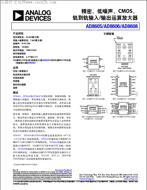
4
9 –IN C 8 OUT C
AD8605 ONLY
图3. 5引脚WLCSP(CB后缀)
图4. 14引脚SOIC_N(R后缀)
OUT A –IN A +IN A V+ +IN B –IN B OUT B 1 14 OUT D –IN D +IN D V– +IN C –IN C OUT C
7
8
图5. 8引脚MSOP(RM后缀)、 8引脚SOIC_N(R后缀)
V+ OUT B –IN B +IN B
AD8608
TOP VIEW (Not to Scale)
02731-003
元器件交易网
AD8605/AD8606/AD8608
目录
特性 ...................................................................................................... 1 应用 ...................................................................................................... 1 概述 ...................................................................................................... 1 引脚配置 ............................................................................................. 1 修订历史 ............................................................................................. 3 5 V电气规格 ....................................................................................... 4 2.7 V电气规格 .................................................................................... 6 绝对最大额定值 ................................................................................ 8 ESD警告 ......................................................................................... 8 典型性能参数 .................................................................................... 9 应用信息 ........................................................................................... 16 输出反相 ...................................................................................... 16 最大功耗 ...................................................................................... 16 输入过压保护 ............................................................................. 16 总谐波失真加噪声 .................................................................... 16 含源电阻的总噪声 .................................................................... 17 通道隔离 ...................................................................................... 17 容性负载驱动 ............................................................................. 17 光敏度 .......................................................................................... 18 WLCSP组装考虑 ........................................................................ 18 I-V转换应用 ..................................................................................... 19 光电二极管前置放大器应用................................................... 19 音频和PDA应用 ......................................................................... 19 仪表放大器 ................................................................................. 20 DAC转换...................................................................................... 20 外形尺寸 ........................................................................................... 21 订购指南 ...................................................................................... 24
16路高清解码器_产品技术参数
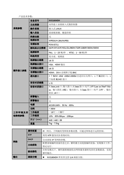
菜单中对于相同设置可进行快捷复制粘贴操作。
开发支持
提供对解码器操作的SDK开发包;提供演示软件,及开发说明。
被动接收
在转发模式下,解码器准确接收由网络服务器转发的任意数据流,实现解码输出。
输出
画面分割
NVS1604DH所有屏支持1/4画面分割。
显示轮巡
NVS1604DH设备同时具备16个VGA接口、16个HDMI接口。
报警
外部报警
具备多路继电器开关量报警输出,便捷实现报警联动外部报警设备(如:现场的灯光)控制,手动控制,联动画面输出。
实时流解码
对编码器本地编码数据实时获取并解码输出。
历史流解码
对编码器本地已经存储的历史数据,获取并解码输出。
信息反馈
各应用端可准确获知当前解码状态。
用户管理
帐号管理
添加、删除、修改用户或者用户组,修改用户密码。
权限管理
对不同的用户,支持设置不同的权限。
安全管理
密码登录;密码出错5次,帐号锁定。
其他
版本信息产品技术参数: Nhomakorabea系统参数
设备型号
NVS1604DH
主处理器
高性能工业级嵌入式微控制器
操作系统
嵌入式LINUX
输入设备
前面板按键,键盘控制
快捷功能
HZ5C2中文资料
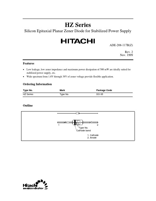
HZ SeriesSilicon Epitaxial Planar Zener Diode for Stabilized Power SupplyADE-208-117B(Z)Rev. 2Nov. 1999 Features•Low leakage, low zener impedance and maximum power dissipation of 500 mW are ideally suited for stabilized power supply, etc.•Wide spectrum from 1.6V through 38V of zener voltage provide flexible application.Ordering InformationType No.Mark Package CodeHZ Series Type No.DO-35OutlineHZ SeriesRev.2, Nov. 1999, page 2 of 8Absolute Maximum Ratings(Ta = 25°C)ItemSymbol Value Unit Power dissipation Pd 500mW Junction temperature Tj 175°C Storage temperatureTstg-55 to +175°CElectrical Characteristics(Ta = 25°C)Zener Voltage Reverese CurrentDynamic Resistance V Z (V)*1TestConditionI R (µA)TestCondition r d (Ω)TestCondition Type Grade Min Max I Z (mA)Max V R (V)Max I Z (mA)HZ2A1 1.6 1.85250.51005A2 1.7 1.9A3 1.8 2.0B1 1.9 2.1550.51005B2 2.0 2.2B3 2.1 2.3C1 2.2 2.4C2 2.3 2.5C32.4 2.6HZ3A1 2.5 2.7550.51005A2 2.6 2.8A3 2.7 2.9B1 2.8 3.0B2 2.9 3.1B3 3.0 3.2C1 3.1 3.3C2 3.2 3.4C33.3 3.5HZ4A1 3.4 3.655 1.01005A2 3.5 3.7A33.63.8Note:1.Tested with DC.HZ SeriesRev.2, Nov. 1999, page 3 of 8Zener Voltage Reverese CurrentDynamic Resistance V Z (V)*1TestConditionI R (µA)TestCondition r d (Ω)TestCondition Type Grade Min Max I Z (mA)Max V R (V)Max I Z (mA)HZ4B1 3.7 3.9551.01005B2 3.8 4.0B3 3.9 4.1C1 4.0 4.2C2 4.1 4.3C34.2 4.4HZ5A1 4.3 4.555 1.51005A2 4.4 4.6A3 4.5 4.7B1 4.6 4.8B2 4.7 4.9B3 4.8 5.0C1 4.9 5.1C2 5.0 5.2C35.1 5.3HZ6A1 5.2 5.555 2.0405A2 5.3 5.6A3 5.4 5.7B1 5.5 5.8B2 5.6 5.9B3 5.7 6.0C1 5.8 6.1C2 6.0 6.3C36.1 6.4HZ7A1 6.3 6.651 3.5155A2 6.4 6.7A3 6.6 6.9B1 6.77.0B2 6.97.2B37.07.3Note:1.Tested with DC.HZ SeriesRev.2, Nov. 1999, page 4 of 8Zener Voltage Reverese CurrentDynamic Resistance V Z (V)*1TestConditionI R (µA)TestCondition r d (Ω)TestCondition Type Grade Min Max I Z (mA)Max V R (V)Max I Z (mA)HZ7C17.27.6513.5155C27.37.7C37.57.9HZ9A17.78.151 5.0205A27.98.3A38.18.5B18.38.7B28.58.9B38.79.1C18.99.3C29.19.5C39.39.7HZ11A19.59.9517.5255A29.710.1A39.910.3B110.210.6B210.410.8B310.711.1C110.911.3C211.111.6C311.411.9HZ12A111.612.1519.5355A211.912.4A312.212.7B112.412.9B212.613.1B312.913.4C113.213.7C213.514.0C313.814.3Note:1.Tested with DC.HZ SeriesRev.2, Nov. 1999, page 5 of 8Zener Voltage Reverese CurrentDynamic Resistance V Z (V)*1TestConditionI R (µA)TestCondition r d (Ω)TestCondition Type Grade Min Max I Z (mA)Max V R (V)Max I Z (mA)HZ15114.114.75111.0405214.515.1314.915.5HZ16115.315.95112.0455215.716.5316.317.1HZ18116.917.75113.0555217.518.3318.119.0HZ20118.819.72115.0602219.520.4320.221.1HZ22120.921.92117.0652221.622.6322.323.3HZ24122.924.02119.0702223.624.7324.325.5HZ27125.226.62121.0802226.227.6327.228.6HZ30128.229.62123.01002229.230.6330.231.6HZ33131.232.62125.01202232.233.6333.234.6HZ36134.235.72127.01402235.336.8336.438.0Note: 1.Tested with DC.Note:2.Type No. is as follows; HZ2B1, HZ2B2, HZ36-3.HZ SeriesMain CharacteristicRev.2, Nov. 1999, page 6 of 8HZ Series Package DimensionsRev.2, Nov. 1999, page 7 of 8HZ SeriesRev.2, Nov. 1999, page 8 of 8Disclaimer1.Hitachi neither warrants nor grants licenses of any rights of Hitachi’s or any third party’s patent,copyright, trademark, or other intellectual property rights for information contained in this document.Hitachi bears no responsibility for problems that may arise with third party’s rights, including intellectual property rights, in connection with use of the information contained in this document.2.Products and product specifications may be subject to change without notice. Confirm that you have received the latest product standards or specifications before final design, purchase or use.3.Hitachi makes every attempt to ensure that its products are of high quality and reliability. However,contact Hitachi’s sales office before using the product in an application that demands especially high quality and reliability or where its failure or malfunction may directly threaten human life or cause risk of bodily injury, such as aerospace, aeronautics, nuclear power, combustion control, transportation,traffic, safety equipment or medical equipment for life support.4.Design your application so that the product is used within the ranges guaranteed by Hitachi particularly for maximum rating, operating supply voltage range, heat radiation characteristics, installationconditions and other characteristics. Hitachi bears no responsibility for failure or damage when used beyond the guaranteed ranges. Even within the guaranteed ranges, consider normally foreseeable failure rates or failure modes in semiconductor devices and employ systemic measures such as fail-safes, so that the equipment incorporating Hitachi product does not cause bodily injury, fire or other consequential damage due to operation of the Hitachi product.5.This product is not designed to be radiation resistant.6.No one is permitted to reproduce or duplicate, in any form, the whole or part of this document without written approval from Hitachi.7.Contact Hitachi’s sales office for any questions regarding this document or Hitachi semiconductor products.Sales OfficesHitachi, Ltd.Semiconductor & Integrated CircuitsNippon Bldg., 2-6-2, Ohte-machi, Chiyoda-ku, Tokyo 100-0004, Japan Tel: (03) 3270-2111 Fax: (03) 3270-5109Copyright © Hitachi, Ltd., 2001. All rights reserved. Printed in Japan.Hitachi Asia Ltd. Hitachi Tower16 Collyer Quay #20-00 Singapore 049318Tel : <65>-538-6533/538-8577 Fax : <65>-538-6933/538-3877URL : .sg URLNorthAmerica : /Europe : /hel/ecg Asia : Japan : http://www.hitachi.co.jp/Sicd/indx.htmHitachi Asia Ltd.(Taipei Branch Office)4/F, No. 167, Tun Hwa North Road Hung-Kuo Building Taipei (105), Taiwan Tel : <886>-(2)-2718-3666 Fax : <886>-(2)-2718-8180 Telex : 23222 HAS-TPURL : Hitachi Asia (Hong Kong) Ltd.Group III (Electronic Components) 7/F., North TowerWorld Finance Centre,Harbour City, Canton Road Tsim Sha Tsui, Kowloon Hong KongTel : <852>-(2)-735-9218 Fax : <852>-(2)-730-0281URL : Hitachi Europe GmbHElectronic Components Group Dornacher Straße 3D-85622 Feldkirchen, Munich GermanyTel: <49> (89) 9 9180-0Fax: <49> (89) 9 29 30 00Hitachi Europe Ltd.Electronic Components Group Whitebrook ParkLower Cookham Road MaidenheadBerkshire SL6 8YA, United Kingdom Tel: <44> (1628) 585000Fax: <44> (1628) 585200Hitachi Semiconductor (America) Inc.179 East Tasman Drive San Jose,CA 95134 Tel: <1> (408) 433-1990Fax: <1>(408) 433-0223For further information write to:Colophon 4.0。
EK 说明书中文版

1 3.7
3 9
3.7.2
3
8
3.7
3.7.1 Status1
System Status 4
5
13 3
3.7.1
2.2.2
8
2.3.1
2.3.1
2.3.1 DC
9
EK 220
2.3.2
ENTER
---X---
ENTER ENTER X
10
2.4 EK220
2.4.1
3.9 2.4.2
6.6.1
2.3.2
CW1.B CW1.E EK220
14 p
MODEM
1
3.12
2
St.1
VbMP
Qb SC.Qb 3.1
QbUW QbLW
3.1
Qb
2 E2 L2.E2 SpE2
3.10
MdME2, SC.E2, L1.E2,
EK220
Elster AS-200
WinPADS
2
3.12 CW2.B CW2.E
ST.1
p.LW
p.UW
3.7.2
ST.7
6
p.Mes
1
p 3.7.2
p.F 3.1
18
3.11 pMin pMax
p.Mes
p.Mes
MRL.p MRU.p
3.6
p.Mes p.F
p.Mes
pMin=pmax
p.F p.Mes
p.F pb
p=p.F
Md.p Md.P= 1
p.Mes Md.P= 1
Typ.p SNP
T.MP
15
AD C K Ho.b CO2 H2 Rhob K.F Md.K
T8XX-XXXH中文资料

®1/11Table 1: Main FeaturesDESCRIPTIONAvailable either in through-hole or surface-mount packages, the BTA08, BTB08 and T8 triac series is suitable for general purpose AC switching. They can be used as an ON/OFF function in applica-tions such as static relays, heating regulation, in-duction motor starting circuits... or for phase control operation in light dimmers, motor speed controllers,...The snubberless versions (BTA/BTB...W and T8series) are specially recommended for use on inductive loads, thanks to their high commutation performances.Logic level versions are designed to interface directly with low power drivers such as microcontrollers.By using an internal ceramic pad, the BTA series provides voltage insulated tab (rated at 2500V RMS ) complying with UL standards (file ref.:E81734).Symbol Value Unit I T(RMS)8A V DRM /V RRM 600 and 800V I GT (Q 1)5 to 50mABTA08, BTB08 and T8 Series8A TRIAC SREV. 6February 2006SNUBBERLESS™, LOGIC LEVEL & STANDARDTable 2: Order CodesPart Number Marking BTA08-xxxxxRG See page table 8 onpage 10BTB08-xxxxxRG T8xx-xxxG T8xx-xxxH T8xx-xxxBBTA08, BTB08 and T8 Series2/11Table 3: Absolute Maximum Ratings Tables 4: Electrical Characteristics (T j = 25°C, unless otherwise specified)■SNUBBERLESS and Logic Level (3 quadrants)Symbol ParameterValue Unit I T(RMS)RMS on-state current (full sine wave)IPAK/D 2PAK/DPAK/TO-220AB T c = 110°C 8ATO-220AB Ins.T c = 100°C I TSM Non repetitive surge peak on-state current (full cycle, T j initial = 25°C) F = 50 Hz t = 20 ms 80A F = 60 Hz t = 16.7 ms84I ²t I ²t Value for fusingt p = 10 ms 36A ²s dI/dt Critical rate of rise of on-state cur-rent I G = 2 x I GT , t r ≤ 100 ns F = 120 Hz T j = 125°C 50A/µs I GM Peak gate currentt p = 20 µsT j = 125°C 4A P G(AV)Average gate power dissipation T j = 125°C1W T stg T jStorage junction temperature rangeOperating junction temperature range- 40 to + 150- 40 to + 125°CSymbol Test ConditionsQuad-rantT8BTA08 / BTB08Unit T810T835TW SW CW BW I GT (1)V D = 12 V R L = 30 ΩI - II -III MAX.10355103550mA V GT I - II - III MAX.1.3V V GD V D = V DRM R L = 3.3 k ΩT j = 125°C I - II - IIIMIN.0.2V I H (2)I T = 100 mA MAX.153510153550mA I L I G = 1.2 I GTI - III MAX.255010255070mAII306015306080dV/dt (2)V D = 67 %V DRM gate open T j = 125°CMIN.4040020404001000V/µs (dI/dt)c (2)(dV/dt)c = 0.1 V/µs T j = 125°CMIN.5.4- 3.5 5.4--A/ms(dV/dt)c = 10 V/µs T j = 125°C2.8- 1.5 2.98--Without snubber T j = 125°C- 4.5-- 4.57BTA08, BTB08 and T8 Series3/11■Standard (4 quadrants)Table 5: Static Characteristics Table 6: Thermal resistance Symbol Test ConditionsQuadrant BTA08 / BTB08Unit C B I GT (1)V D = 12 V R L = 30 ΩI - II - III IV MAX.255050100mA V GT ALL MAX. 1.3V V GD V D = V DRM R L = 3.3 k Ω T j = 125°C ALLMIN.0.2V I H (2)I T = 500 mA MAX.2550mA I L I G = 1.2 I GTI - III - IVMAX.4050mA II80100dV/dt (2)V D = 67 %V DRM gate open T j = 125°CMIN.200400V/µs (dV/dt)c (2)(dI/dt)c = 5.3 A/ms T j = 125°C MIN.510V/µsSymbol Test ConditionsValueUnit V T (2)I TM = 11 A t p = 380 µs T j = 25°C MAX. 1.55V V to (2)Threshold voltage T j = 125°C MAX.0.85V R d (2)Dynamic resistance T j = 125°C MAX.50m ΩI DRM I RRMV DRM = V RRMT j = 25°C MAX.5µA T j = 125°C1mANote 1: minimum I GT is guaranted at 5% of I GT max.Note 2: for both polarities of A2 referenced to A1.Symbol ParameterValue Unit R th(j-c)Junction to case (AC)IPAK / D 2PAK / DPAK / TO-220AB 1.6°C/WTO-220AB Insulated 2.5R th(j-a)Junction to ambientS = 1 cm ²D 2PAK 45°C/WS = 0.5 cm ²DPAK70TO-220AB / TO-220AB Insulated 60IPAK100S = Copper surface under tab.BTA08, BTB08 and T8 Series4/11Figure 1: Maximum power dissipation versus RMS on-state current (full cycle)Figure 2: RMS on-state current versus case temperature (full cycle)Figure 3: RMS on-state current versus ambient temperature (printed circuit board FR4, copper thickness: 35µm) (full cycle)Figure 4: Relative variation of thermal impedance versus pulse durationFigure 5: On-state characteristics (maximum values)Figure 6: Surge peak on-state current versus number of cyclesBTA08, BTB08 and T8 Series5/11Figure 7: Non-repetitive surge peak on-state current for a sinusoidal pulse with width t p < 10 ms and corresponding value of I 2tFigure 8: Relative variation of gate trigger current, holding current and latching current versus junction temperature (typical values)Figure 9: Relative variation of critical rate of decrease of main current versus (dV/dt)c (typical values) (Snubberless & L ogic level types)Figure 10: Relative variation of critical rate of decrease of main current versus (dV/dt)c (typical values) (Standard types)Figure 11: Relative variation of critical rate of decrease of main current versus junction temperatureFigure 12: DPAK and D 2P AK Thermal resistance junction to ambient versus copper surface under tab (printed circuit board FR4, copper thickness:35µm)BTA08, BTB08 and T8 Series6/11Figure 13: Ordering Information Scheme (BTA08 and BTB08 series)Figure 14: Ordering Information Scheme (T8 series)Table 7: Product SelectorPart NumberVoltage (xxx)Sensitivity Type Package 600 V 800 V BTA/BTB08-xxxB X X 50 mA Standard TO-220AB BTA/BTB08-xxxBW X X 50 mA Snubberless TO-220AB BTA/BTB08-xxxC X X 25 mAStandard TO-220AB BTA/BTB08-xxxCW X X 35 mA Snubberless TO-220AB BTA/BTB08-xxxSW X X 10 mA Logic level TO-220AB BTA/BTB08-xxxTW X X 5 mA Logic Level TO-220AB T810-xxxG X X 10 mA Logic Level D2PAK T810-xxxH X X 10 mA Logic Level IPAK T835-xxxB X X 35 mA Snubberless DPAK T835-xxxG X X 35 mA Snubberless D 2PAK T835-xxxHXX35 mASnubberlessIPAKBTB: non insulated TO-220AB packageBTA08, BTB08 and T8 Series Figure 15: D2PAK Package Mechanical DataFigure 16: D2PAK Foot Print Dimensions(in millimeters)7/11BTA08, BTB08 and T8 SeriesFigure 17: DPAK Package Mechanical DataFigure 18: DPAK Foot Print Dimensions (in millimeters)8/11BTA08, BTB08 and T8 Series9/11BTA08, BTB08 and T8 Series10/11In order to meet environmental requirements, ST offers these devices in ECOPACK® packages. These packages have a Lead-free second level interconnect . The category of second level interconnect is marked on the package and on the inner box label, in compliance with JEDEC Standard JESD97. The maximum ratings related to soldering conditions are also marked on the inner box label. ECOPACK is an ST trademark. ECOPACK specifications are available at: .Table 8: Ordering InformationOrdering type Marking Package Weight Base qtyDelivery modeBTA/BTB08-xxxyzRGBTA/BTB08-xxxyzTO-220AB 2.3 g 50Tube T8yy-xxxG T8yyxx D 2PAK 1.5 g 50Tube T8yy-xxxG-TR T8yyxx 1000Tape & reel T8yy-xxxB T8yyxx DPAK 0.3 g 75Tube T8yy-xxxB-TR T8yyxx 2500Tape & reel T8yy-xxxHT8yyxxIPAK0.4 g75TubeNote: xxx = voltage, yy = sensitivity, z = typeTable 9: Revision HistoryDate Revision Description of ChangesApr-20025A Last update.13-Feb-20066TO-220AB delivery mode changed from bulk to tube.ECOPACK statement added.元器件交易网BTA08, BTB08 and T8 Series Information furnished is believed to be accurate and reliable. However, STMicroelectronics assumes no responsibility for the consequencesof use of such information nor for any infringement of patents or other rights of third parties which may result from its use. No license is grantedby implication or otherwise under any patent or patent rights of STMicroelectronics. Specifications mentioned in this publication are subjectto change without notice. This publication supersedes and replaces all information previously supplied. STMicroelectronics products are notauthorized for use as critical components in life support devices or systems without express written approval of STMicroelectronics.The ST logo is a registered trademark of STMicroelectronics.All other names are the property of their respective owners© 2006 STMicroelectronics - All rights reservedSTMicroelectronics group of companiesAustralia - Belgium - Brazil - Canada - China - Czech Republic - Finland - France - Germany - Hong Kong - India - Israel - Italy - Japan - Malaysia - Malta - Morocco - Singapore - Spain - Sweden - Switzerland - United Kingdom - United States of America11/11。
mspg2231中文资料
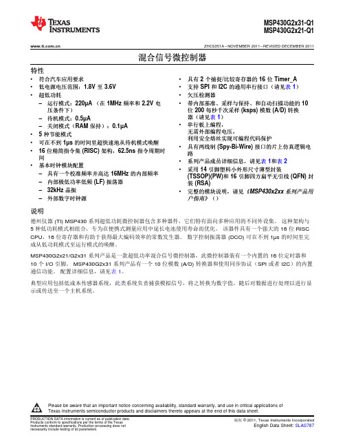
MSP430G2x31-Q1MSP430G2x21-Q1 ZHCS351A–NOVEMBER2011–REVISED DECEMBER2011混合信号微控制器特性•符合汽车应用要求•具有2个捕捉/比较寄存器的16位Timer_A•低电源电压范围:1.8V至3.6V•支持SPI和I2C的通用串行接口(请见表1)•超低功耗•欠压检测器–运行模式:220μA(在1MHz频率和2.2V电•带内部基准、采样与保持、和自动扫描功能的10压条件下)位200每秒千次采样(ksps)模数(A/D)转换器(请见表1)–待机模式:0.5μA•串行板上编程,–关闭模式(RAM保持):0.1μA无需外部编程电压,•5种节能模式利用安全熔丝实现可编程代码保护•可在不到1μs的时间里超快速地从待机模式唤醒•具有两线制(Spy-Bi-Wire)接口的片上仿真逻辑电•16位精简指令集(RISC)架构,62.5ns指令周期时路间•系列产品成员详细信息,请见表1和表2•基本时钟模块配置•采用14引脚塑料小外形尺寸薄型封装–具有一个校准频率并高达16MHz的内部频率(TSSOP)(PW)和16引脚四方扁平无引线(QFN)封–内部极低功率低频(LF)振荡器装(RSA)–32kHz晶振•完整的模块说明,请见《MSP430x2xx系列产品用–外部数字时钟源户指南》()说明德州仪器(TI)MSP430系列超低功耗微控制器包含多种器件,它们特有面向多种应用的不同外设集。
这种架构与5种低功耗模式相组合,专为在便携式测量应用中延长电池使用寿命而优化。
该器件具有一个强大的16位RISC CPU,16位寄存器和有助于获得最大编码效率的常数发生器。
数字控制振荡器(DCO)可在不到1µs的时间里完成从低功耗模式至运行模式的唤醒。
MSP430G2x21/G2x31系列产品是一款超低功率混合信号微控制器,此微控制器装有一个内置的16位定时器和10个I/O引脚。
LM337LM中文资料
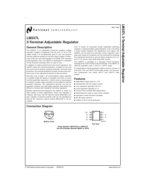
LM337L3-Terminal Adjustable RegulatorGeneral DescriptionThe LM337L is an adjustable 3-terminal negative voltage regulator capable of supplying 100mA over a 1.2V to 37V output range.It is exceptionally easy to use and requires only two external resistors to set the output voltage.Further-more,both line and load regulation are better than standard fixed regulators.Also,the LM337L is packaged in a standard TO-92transistor package which is easy to use.In addition to higher performance than fixed regulators,the LM337L offers full overload protection.Included on the chip are current limit,thermal overload protection and safe area protection.All overload protection circuitry remains fully func-tional even if the adjustment terminal is disconnected.Normally,only a single 1µF solid tantalum output capacitor is needed unless the device is situated more than 6inches from the input filter capacitors,in which case an input bypass is needed.A larger output capacitor can be added to improve transient response.The adjustment terminal can be by-passed to achieve very high ripple rejection ratios which are difficult to achieve with standard 3-terminal regulators.Besides replacing fixed regulators,the LM337L is useful in a wide variety of other applications.Since the regulator is “floating”and sees only the input-to-output differential volt-age,supplies of several hundred volts can be regulated as long as the maximum input-to-output differential is not ex-ceeded.Also,it makes an especially simple adjustable switching regulator,a programmable output regulator,or by connecting a fixed resistor between the adjustment and output,the LM337L can be used as a precision current regulator.Sup-plies with electronic shutdown can be achieved by clamping the adjustment terminal to ground which programs the out-put to 1.2V where most loads draw little current.The LM337L is available in a standard TO-92transistor package and a SO-8surface mount package.The LM337L is rated for operation over a −25˚C to +125˚C range.For applications requiring greater output current in excess of 0.5A and 1.5A,see LM137series data sheets.For the posi-tive complement,see series LM117and LM317L data sheets.Featuresn Adjustable output down to 1.2V n Guaranteed 100mA output current n Line regulation typically 0.01%/V n Load regulation typically 0.1%n Current limit constant with temperaturen Eliminates the need to stock many voltages n Standard 3-lead transistor package n 80dB ripple rejectionnOutput is short circuit protectedConnection DiagramDS009134-1Bottom ViewDS009134-2Top ViewOrder Number LM337LM or LM337LZ See NS Package Number M08A or Z03AMay 1998LM337L 3-Terminal Adjustable Regulator©1999National Semiconductor Corporation Absolute Maximum Ratings(Note1)If Military/Aerospace specified devices are required, please contact the National Semiconductor Sales Office/ Distributors for availability and specifications.Power Dissipation Internally Limited Input–Output Voltage Differential40V Operating JunctionTemperature Range−25˚C to+125˚C Storage Temperature−55˚C to+150˚C Lead Temperature(Soldering,10sec.)300˚C Plastic Package(Soldering4sec.)260˚C ESD rating to be determined.Electrical Characteristics(Note2)Parameter Conditions Min Typ Max Units Line Regulation T A=25˚C,3V≤|V IN−V OUT|≤40V,0.010.04%/V(Note3)Load Regulation T A=25˚C,5mA≤I OUT≤I MAX,(Note3)0.10.5% Thermal Regulation T A=25˚C,10ms Pulse0.040.2%/W Adjustment Pin Current50100µA Adjustment Pin Current Change5mA≤I L≤100mA0.25µA3V≤|V IN−V OUT|≤40VReference Voltage3V≤|V IN−V OUT|≤40V,(Note4) 1.20 1.25 1.30V10mA≤I OUT≤100mA,P≤625mWLine Regulation3V≤|V IN−V OUT|≤40V,(Note3)0.020.07%/V Load Regulation5mA≤I OUT≤100mA,(Note3)0.3 1.5% Temperature Stability T MIN≤T j≤T MAX0.65% Minimum Load Current|V IN−V OUT|≤40V 3.55mA3V≤|V IN−V OUT|≤15V 2.2 3.5mA Current Limit3V≤|V IN−V OUT|≤13V100200320mA|V IN−V OUT|=40V2550120mA Rms Output Noise,%of V OUT T A=25˚C,10Hz≤f≤10kHz0.003% Ripple Rejection Ratio V OUT=−10V,F=120Hz,C ADJ=065dBC ADJ=10µF6680dBLong-Term Stability T A=125˚C0.31% Note1:“Absolute Maximum Ratings”indicate limits beyond which damage to the device may occur.Operating Ratings indicate conditions for which the device is functional,but do not guarantee specific performance limits.Note2:Unless otherwise specified,these specifications apply−25˚C≤T j≤+125˚C for the LM337L;|V IN−V OUT|=5V and I OUT=40mA.Although power dissi-pation is internally limited,these specifications are applicable for power dissipations up to625mW.I MAX is100mA.Note3:Regulation is measured at constant junction temperature,using pulse testing with a low duty cycle.Changes in output voltage due to heating effects are cov-ered under the specification for thermal regulation.Note4:Thermal resistance of the TO-92package is180˚C/W junction to ambient with0.4"leads from a PC board and160˚C/W junction to ambient with0.125"lead length to PC board.The M packageθJA is180˚C/W in still air.2Typical Applications1.2V-25V Adjustable RegulatorDS009134-3Full output current not available at high input-output voltages†C1=1µF solid tantalum or10µF aluminum electrolytic required forstability*C2=1µF solid tantalum is required only if regulator is more than4"frompower supply filter capacitorRegulator with Trimmable Output VoltageDS009134-4Trim Procedure:—If V OUT is−23.08V or bigger,cut out R3(if smaller,don’t cut it out).—Then if V OUT is−22.47V or bigger,cut out R4(if smaller,don’t).—Then if V OUT is−22.16V or bigger,cut out R5(if smaller,don’t).This will trim the output to well within1%of−22.00V DC,without any of theexpense or trouble of a trim pot(see LB-46).Of course,this technique canbe used at any output voltage level.3Physical Dimensions inches(millimeters)unless otherwise notedSO-8Plastic Package(M)Order Number LM337LMNS Package Number M08ATO-92Plastic Package(Z)Order Number LM337LZNS Package Number Z03A 4NotesLIFE SUPPORT POLICYNATIONAL’S PRODUCTS ARE NOT AUTHORIZED FOR USE AS CRITICAL COMPONENTS IN LIFE SUPPORT DEVICES OR SYSTEMS WITHOUT THE EXPRESS WRITTEN APPROVAL OF THE PRESIDENT AND GENERAL COUNSEL OF NATIONAL SEMICONDUCTOR CORPORATION.As used herein:1.Life support devices or systems are devices orsystems which,(a)are intended for surgical implant into the body,or(b)support or sustain life,and whose failure to perform when properly used in accordance with instructions for use provided in the labeling,can be reasonably expected to result in a significant injury to the user.2.A critical component is any component of a lifesupport device or system whose failure to perform can be reasonably expected to cause the failure of the life support device or system,or to affect its safety or effectiveness.National Semiconductor CorporationAmericasTel:1-800-272-9959 Fax:1-800-737-7018 Email:support@ National SemiconductorEuropeFax:+49(0)180-5308586Email:europe.support@Deutsch Tel:+49(0)180-5308585English Tel:+49(0)180-5327832Français Tel:+49(0)180-5329358Italiano Tel:+49(0)180-5341680National SemiconductorAsia Pacific CustomerResponse GroupTel:65-2544466Fax:65-2504466Email:sea.support@National SemiconductorJapan Ltd.Tel:81-3-5639-7560Fax:81-3-5639-7507 LM337L 3-Terminal Adjustable RegulatorNational does not assume any responsibility for use of any circuitry described,no circuit patent licenses are implied and National reserves the right at any time without notice to change said circuitry and specifications.。
最新BL1616(LED驱动芯片)中文资料
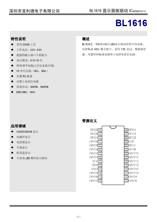
逻辑电源
25
GRID0—GRID15
输出(位)
4-8,12-22
GND
逻辑地
11
注:SEG 引脚连接 LED 阳极,GRID 引脚连接 LED 阴极。
说明 I2C 总线串行接口的时钟输入 I2C 总线串行接口的数据输入 段输出 5V±10% 位输出 系统地
-2-
电气参数
极限参数(Ta = 25℃)
Command2(byte2) ack stop
SCL
SDA
Command1
start
ack
Data1
Command1
ack stop start
ack
Command1:设置地址 Data1~n : 传输显示数据 Command2:控制显示
DataN
Command2(byte1)
ack stop start
bl1616显示面板驱动icisos2013v10电气参数极限参数ta25参数符号范围单位逻辑电源电压vdd0570逻辑输入电压vi105vddledseg驱动输出电流io180maledgrid驱动输出电流io2700ma工作温度topt4080储存温度tstg6515025参数符号最小典型最大单位测试条件逻辑电源电压vdd33高电平输入电压vih07vdd低电平输入电压vil静态电流idd08mavdd50v无负载显示关sdascl上拉电阻rsdarscl12seg驱动电流isegmavdd50vseg电阻对gndgrid驱动电流igridmavdd50vgrid电阻对vddgrid频率fgridhzvdd50v上升时间ttzhsegnsvdd50vsegn接100下拉电阻gridn接100上拉电阻cl15pfttlzgridns下降时间tthzsegnsttzlgridns最大时钟频率fclkmaxmhz占空比50bl1616显示面板驱动icisos2013v1025参数符号最小典型最大单位测试条件时钟脉冲宽度pwclk400数据建立时间tsetup100数据保持时间thold100ack脉冲宽度tackbl1616显示面板驱动icisos2013v10显示寄存器该寄存器存储通过串行接口从外部器件传送到bl1616的数据从数据字节的高位到低位进行写操作地址分配如下
80021012A资料
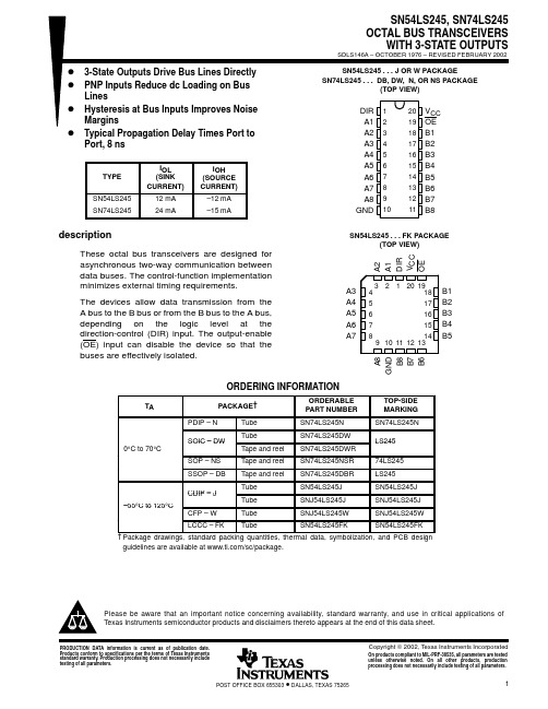
PACKAGING INFORMATIONOrderable Device Status(1)PackageType PackageDrawingPins PackageQtyEco Plan(2)Lead/Ball Finish MSL Peak Temp(3)5962-8002101VRA ACTIVE CDIP J201None Call TI Level-NC-NC-NC 5962-8002101VSA ACTIVE CFP W201None Call TI Level-NC-NC-NC 80021012A ACTIVE LCCC FK201None Call TI Level-NC-NC-NC 8002101SA ACTIVE CFP W201None Call TI Level-NC-NC-NC JM38510/32803B2A ACTIVE LCCC FK201None Call TI Level-NC-NC-NC JM38510/32803BRA ACTIVE CDIP J201None Call TI Level-NC-NC-NC JM38510/32803BSA ACTIVE CFP W201None Call TI Level-NC-NC-NC SN54LS245J ACTIVE CDIP J201None Call TI Level-NC-NC-NCSN74LS245DBR ACTIVE SSOP DB202000Pb-Free(RoHS)CU NIPDAU Level-2-260C-1YEAR/Level-1-235C-UNLIMSN74LS245DW ACTIVE SOIC DW2025Pb-Free(RoHS)CU NIPDAU Level-2-250C-1YEAR/Level-1-235C-UNLIMSN74LS245DWR ACTIVE SOIC DW202000Pb-Free(RoHS)CU NIPDAU Level-2-250C-1YEAR/Level-1-235C-UNLIMSN74LS245J OBSOLETE CDIP J20None Call TI Call TISN74LS245N ACTIVE PDIP N2020Pb-Free(RoHS)CU NIPDAU Level-NC-NC-NC SN74LS245N3OBSOLETE PDIP N20None Call TI Call TISN74LS245NSR ACTIVE SO NS202000Pb-Free(RoHS)CU NIPDAU Level-2-260C-1YEAR/Level-1-235C-UNLIMSNJ54LS245FK ACTIVE LCCC FK201None Call TI Level-NC-NC-NC SNJ54LS245J ACTIVE CDIP J201None Call TI Level-NC-NC-NC SNJ54LS245W ACTIVE CFP W201None Call TI Level-NC-NC-NC(1)The marketing status values are defined as follows:ACTIVE:Product device recommended for new designs.LIFEBUY:TI has announced that the device will be discontinued,and a lifetime-buy period is in effect.NRND:Not recommended for new designs.Device is in production to support existing customers,but TI does not recommend using this part in a new design.PREVIEW:Device has been announced but is not in production.Samples may or may not be available.OBSOLETE:TI has discontinued the production of the device.(2)Eco Plan-May not be currently available-please check /productcontent for the latest availability information and additional product content details.None:Not yet available Lead(Pb-Free).Pb-Free(RoHS):TI's terms"Lead-Free"or"Pb-Free"mean semiconductor products that are compatible with the current RoHS requirements for all6substances,including the requirement that lead not exceed0.1%by weight in homogeneous materials.Where designed to be soldered at high temperatures,TI Pb-Free products are suitable for use in specified lead-free processes.Green(RoHS&no Sb/Br):TI defines"Green"to mean"Pb-Free"and in addition,uses package materials that do not contain halogens, including bromine(Br)or antimony(Sb)above0.1%of total product weight.(3)MSL,Peak Temp.--The Moisture Sensitivity Level rating according to the JEDECindustry standard classifications,and peak solder temperature.Important Information and Disclaimer:The information provided on this page represents TI's knowledge and belief as of the date that it is provided.TI bases its knowledge and belief on information provided by third parties,and makes no representation or warranty as to the accuracy of such information.Efforts are underway to better integrate information from third parties.TI has taken and continues to take reasonable steps to provide representative and accurate information but may not have conducted destructive testing or chemical analysis on incoming materials and chemicals.TI and TI suppliers consider certain information to be proprietary,and thus CAS numbers and other limited information may not be available for release.In no event shall TI's liability arising out of such information exceed the total purchase price of the TI part(s)at issue in this document sold by TIto Customer on an annual basis.IMPORTANT NOTICETexas Instruments Incorporated and its subsidiaries (TI) reserve the right to make corrections, modifications, enhancements, improvements, and other changes to its products and services at any time and to discontinue any product or service without notice. Customers should obtain the latest relevant information before placing orders and should verify that such information is current and complete. All products are sold subject to TI’s terms and conditions of sale supplied at the time of order acknowledgment.TI warrants performance of its hardware products to the specifications applicable at the time of sale in accordance with TI’s standard warranty. T esting and other quality control techniques are used to the extent TI deems necessary to support this warranty. Except where mandated by government requirements, testing of all parameters of each product is not necessarily performed.TI assumes no liability for applications assistance or customer product design. Customers are responsible for their products and applications using TI components. T o minimize the risks associated with customer products and applications, customers should provide adequate design and operating safeguards.TI does not warrant or represent that any license, either express or implied, is granted under any TI patent right, copyright, mask work right, or other TI intellectual property right relating to any combination, machine, or process in which TI products or services are used. Information published by TI regarding third-party products or services does not constitute a license from TI to use such products or services or a warranty or endorsement thereof. Use of such information may require a license from a third party under the patents or other intellectual property of the third party, or a license from TI under the patents or other intellectual property of TI.Reproduction of information in TI data books or data sheets is permissible only if reproduction is without alteration and is accompanied by all associated warranties, conditions, limitations, and notices. Reproduction of this information with alteration is an unfair and deceptive business practice. TI is not responsible or liable for such altered documentation.Resale of TI products or services with statements different from or beyond the parameters stated by TI for that product or service voids all express and any implied warranties for the associated TI product or service and is an unfair and deceptive business practice. TI is not responsible or liable for any such statements. Following are URLs where you can obtain information on other Texas Instruments products and application solutions:Products ApplicationsAmplifiers Audio /audioData Converters Automotive /automotiveDSP Broadband /broadbandInterface Digital Control /digitalcontrolLogic Military /militaryPower Mgmt Optical Networking /opticalnetwork Microcontrollers Security /securityTelephony /telephonyVideo & Imaging /videoWireless /wirelessMailing Address:Texas InstrumentsPost Office Box 655303 Dallas, Texas 75265Copyright 2005, Texas Instruments Incorporated。
- 1、下载文档前请自行甄别文档内容的完整性,平台不提供额外的编辑、内容补充、找答案等附加服务。
- 2、"仅部分预览"的文档,不可在线预览部分如存在完整性等问题,可反馈申请退款(可完整预览的文档不适用该条件!)。
- 3、如文档侵犯您的权益,请联系客服反馈,我们会尽快为您处理(人工客服工作时间:9:00-18:30)。
HZ SeriesSilicon Epitaxial Planar Zener Diode for Stabilized Power SupplyADE-208-117B(Z)Rev. 2Nov. 1999 Features•Low leakage, low zener impedance and maximum power dissipation of 500 mW are ideally suited for stabilized power supply, etc.•Wide spectrum from 1.6V through 38V of zener voltage provide flexible application.Ordering InformationType No.Mark Package CodeHZ Series Type No.DO-35OutlineHZ SeriesRev.2, Nov. 1999, page 2 of 8Absolute Maximum Ratings(Ta = 25°C)ItemSymbol Value Unit Power dissipation Pd 500mW Junction temperature Tj 175°C Storage temperatureTstg-55 to +175°CElectrical Characteristics(Ta = 25°C)Zener Voltage Reverese CurrentDynamic Resistance V Z (V)*1TestConditionI R (µA)TestCondition r d (Ω)TestCondition Type Grade Min Max I Z (mA)Max V R (V)Max I Z (mA)HZ2A1 1.6 1.85250.51005A2 1.7 1.9A3 1.8 2.0B1 1.9 2.1550.51005B2 2.0 2.2B3 2.1 2.3C1 2.2 2.4C2 2.3 2.5C32.4 2.6HZ3A1 2.5 2.7550.51005A2 2.6 2.8A3 2.7 2.9B1 2.8 3.0B2 2.9 3.1B3 3.0 3.2C1 3.1 3.3C2 3.2 3.4C33.3 3.5HZ4A1 3.4 3.655 1.01005A2 3.5 3.7A33.63.8Note:1.Tested with DC.HZ SeriesRev.2, Nov. 1999, page 3 of 8Zener Voltage Reverese CurrentDynamic Resistance V Z (V)*1TestConditionI R (µA)TestCondition r d (Ω)TestCondition Type Grade Min Max I Z (mA)Max V R (V)Max I Z (mA)HZ4B1 3.7 3.9551.01005B2 3.8 4.0B3 3.9 4.1C1 4.0 4.2C2 4.1 4.3C34.2 4.4HZ5A1 4.3 4.555 1.51005A2 4.4 4.6A3 4.5 4.7B1 4.6 4.8B2 4.7 4.9B3 4.8 5.0C1 4.9 5.1C2 5.0 5.2C35.1 5.3HZ6A1 5.2 5.555 2.0405A2 5.3 5.6A3 5.4 5.7B1 5.5 5.8B2 5.6 5.9B3 5.7 6.0C1 5.8 6.1C2 6.0 6.3C36.1 6.4HZ7A1 6.3 6.651 3.5155A2 6.4 6.7A3 6.6 6.9B1 6.77.0B2 6.97.2B37.07.3Note:1.Tested with DC.HZ SeriesRev.2, Nov. 1999, page 4 of 8Zener Voltage Reverese CurrentDynamic Resistance V Z (V)*1TestConditionI R (µA)TestCondition r d (Ω)TestCondition Type Grade Min Max I Z (mA)Max V R (V)Max I Z (mA)HZ7C17.27.6513.5155C27.37.7C37.57.9HZ9A17.78.151 5.0205A27.98.3A38.18.5B18.38.7B28.58.9B38.79.1C18.99.3C29.19.5C39.39.7HZ11A19.59.9517.5255A29.710.1A39.910.3B110.210.6B210.410.8B310.711.1C110.911.3C211.111.6C311.411.9HZ12A111.612.1519.5355A211.912.4A312.212.7B112.412.9B212.613.1B312.913.4C113.213.7C213.514.0C313.814.3Note:1.Tested with DC.HZ SeriesRev.2, Nov. 1999, page 5 of 8Zener Voltage Reverese CurrentDynamic Resistance V Z (V)*1TestConditionI R (µA)TestCondition r d (Ω)TestCondition Type Grade Min Max I Z (mA)Max V R (V)Max I Z (mA)HZ15114.114.75111.0405214.515.1314.915.5HZ16115.315.95112.0455215.716.5316.317.1HZ18116.917.75113.0555217.518.3318.119.0HZ20118.819.72115.0602219.520.4320.221.1HZ22120.921.92117.0652221.622.6322.323.3HZ24122.924.02119.0702223.624.7324.325.5HZ27125.226.62121.0802226.227.6327.228.6HZ30128.229.62123.01002229.230.6330.231.6HZ33131.232.62125.01202232.233.6333.234.6HZ36134.235.72127.01402235.336.8336.438.0Note: 1.Tested with DC.Note:2.Type No. is as follows; HZ2B1, HZ2B2, HZ36-3.HZ SeriesMain CharacteristicRev.2, Nov. 1999, page 6 of 8HZ Series Package DimensionsRev.2, Nov. 1999, page 7 of 8HZ SeriesRev.2, Nov. 1999, page 8 of 8Disclaimer1.Hitachi neither warrants nor grants licenses of any rights of Hitachi’s or any third party’s patent,copyright, trademark, or other intellectual property rights for information contained in this document.Hitachi bears no responsibility for problems that may arise with third party’s rights, including intellectual property rights, in connection with use of the information contained in this document.2.Products and product specifications may be subject to change without notice. Confirm that you have received the latest product standards or specifications before final design, purchase or use.3.Hitachi makes every attempt to ensure that its products are of high quality and reliability. However,contact Hitachi’s sales office before using the product in an application that demands especially high quality and reliability or where its failure or malfunction may directly threaten human life or cause risk of bodily injury, such as aerospace, aeronautics, nuclear power, combustion control, transportation,traffic, safety equipment or medical equipment for life support.4.Design your application so that the product is used within the ranges guaranteed by Hitachi particularly for maximum rating, operating supply voltage range, heat radiation characteristics, installationconditions and other characteristics. Hitachi bears no responsibility for failure or damage when used beyond the guaranteed ranges. Even within the guaranteed ranges, consider normally foreseeable failure rates or failure modes in semiconductor devices and employ systemic measures such as fail-safes, so that the equipment incorporating Hitachi product does not cause bodily injury, fire or other consequential damage due to operation of the Hitachi product.5.This product is not designed to be radiation resistant.6.No one is permitted to reproduce or duplicate, in any form, the whole or part of this document without written approval from Hitachi.7.Contact Hitachi’s sales office for any questions regarding this document or Hitachi semiconductor products.Sales OfficesHitachi, Ltd.Semiconductor & Integrated CircuitsNippon Bldg., 2-6-2, Ohte-machi, Chiyoda-ku, Tokyo 100-0004, Japan Tel: (03) 3270-2111 Fax: (03) 3270-5109Copyright © Hitachi, Ltd., 2001. All rights reserved. Printed in Japan.Hitachi Asia Ltd. Hitachi Tower16 Collyer Quay #20-00 Singapore 049318Tel : <65>-538-6533/538-8577 Fax : <65>-538-6933/538-3877URL : .sg URLNorthAmerica : /Europe : /hel/ecg Asia : Japan : http://www.hitachi.co.jp/Sicd/indx.htmHitachi Asia Ltd.(Taipei Branch Office)4/F, No. 167, Tun Hwa North Road Hung-Kuo Building Taipei (105), Taiwan Tel : <886>-(2)-2718-3666 Fax : <886>-(2)-2718-8180 Telex : 23222 HAS-TPURL : Hitachi Asia (Hong Kong) Ltd.Group III (Electronic Components) 7/F., North TowerWorld Finance Centre,Harbour City, Canton Road Tsim Sha Tsui, Kowloon Hong KongTel : <852>-(2)-735-9218 Fax : <852>-(2)-730-0281URL : Hitachi Europe GmbHElectronic Components Group Dornacher Straße 3D-85622 Feldkirchen, Munich GermanyTel: <49> (89) 9 9180-0Fax: <49> (89) 9 29 30 00Hitachi Europe Ltd.Electronic Components Group Whitebrook ParkLower Cookham Road MaidenheadBerkshire SL6 8YA, United Kingdom Tel: <44> (1628) 585000Fax: <44> (1628) 585200Hitachi Semiconductor (America) Inc.179 East Tasman Drive San Jose,CA 95134 Tel: <1> (408) 433-1990Fax: <1>(408) 433-0223For further information write to:Colophon 4.0。
