HMD4M32M2VE中文资料
HMF2M32M4VGL中文资料
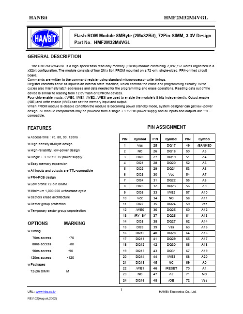
PIN ASSIGNMENTGENERAL DESCRIPTIONThe HMF2M32M4VGL is a high-speed flash read only memory (FROM) module containing 2,097,152 words organized in a x32bit configuration. The module consists of four 2M x 8bit FROM mounted on a 72-pin, single-sided, FR4-printed circuit board.Commands are written to the command register using standard microprocessor write timings.Register contents serve as input to an internal state-machine, which controls the erase and programming circuitry. Write cycles also internally latch addresses and data needed for the programming and erase operations. Reading data out of the device is similar to reading from 12.0V flash or EPROM devices.Four chip enable inputs, (/WE0, /WE1, /WE2, /WE3) are used to enable the module ’s 8 bits independently. Output enable (/OE) and write enable (/WE) can set the memory input and output.When FROM module is disable condition the module is becoming power standby mode, system designer can get low -power design. All module components may be powered from a single +3.3V DC power supply and all inputs and outputs are TTL-compatible.FEATURESPIN Symbol PIN Symbol PIN Symbol 1 Vss 25 DQ17 49 /BANKE0 2 NC 26 DQ18 50 A3 3 DQ0 27 DQ19 51 A4 4 DQ1 28 DQ20 52 A5 5 DQ2 29 DQ21 53 A6 6 DQ3 30 Vcc 54 A7 7 DQ4 31 DQ22 55 A8 8 DQ5 32 DQ23 56 A9 9 DQ6 33 /WE2 57 A10 10 Vcc 34 NC 58 A11 11 DQ7 35 DQ24 59 Vcc 12 /WE0 36 DQ25 60 A12 13 /RY_BY 37 DQ26 61 A13 14 DQ8 38 DQ27 62 A14 15 DQ9 39 Vss 63 A15 16 DQ10 40 DQ28 64 A16 17 DQ11 41 DQ29 65 A17 18 DQ12 42 DQ30 66 A18 19 DQ13 43 DQ31 67 A19 20 DQ14 44 /WE3 68 A20 21 DQ15 45 NC 69 A0 22 /WE1 46 /RESET 70 A1 23 NC 47 A2 71 NC 24DQ1648/OE72Vssw Access time : 70, 80, 90, 120ns w High-density 8MByte design w High-reliability, low-power design w Single + 3.3V ± 0.3V power supply w Easy memory expansionw All inputs and outputs are TTL-compatible w FR4-PCB design w Low profile 72-pin SIMMw Minimum 1,000,000 write/erase cycle w Sectors erase architecture w Sector group protectionw Temporary sector group unprotectionOPTIONS MARKINGw Timing70ns access -70 80ns access -80 90ns access -90 120ns access -120 w Packages72-pin SIMM MFUNCTIONAL BLOCK DIAGRAMDQ0 - DQ31A0 – A19/WE0/WE1/WE2/WE3/OE/ResetTRUTH TABLEMODE/OE /CE /WE /RESET DQ ( /BYTE=L )POWER STANDBY X H X Vcc ±0.3VHIGH-Z STANDBY NOT SELECTED H L H H HIGH-Z ACTIVE READL L H H D OUT ACTIVE WRITE or ERASE XLLHD INACTIVENOTE : X means don ’t careABSOLUTE MAXIMUM RATINGSPARAMETERSYMBOL RATING Voltage with respect to ground all other pins V IN,OUT -0.5V to Vcc+0.5V Voltage with respect to ground Vcc V CC -0.5V to +4.0VStorage TemperatureT STG-65o C to +150o COperating Temperature T A -55o C to +125o CThis is a stress rating only and functional operation of the device at these or any other conditions above those indicated in the operating section of this specification is not implied. Exposure to absolute maximum rating conditions for extended periods may affect reliability.RECOMMENDED DC OPERATING CONDITIONSPARAMETERSYMBOL MIN TYP. MAX Vcc for ± 10% device Supply Voltages Vcc 2.7V 3.6V Ground V SSDC AND OPERATING CHARACTERISTICS ( 0o C ≤ T A ≤ 70 o C )PARAMETERTEST CONDITIONSSYMBOL MIN TYP MAX UNI T Input Load Current Vcc=Vcc max, V IN = Vss to Vcc I L1 ±1.0 µA A9 Input Loda Current Vcc=Vcc max, ; A9=12.5 V I L1T 35 µA Output Leakage CurrentVcc=Vcc max, V OUT = Vss to Vcc I L0±1.0 µA5MHz 9 16 /CE= V IL, /OE= V IH, Byte Mode1MHz 2 4 5MHz 9 16 Vcc Active Read Current (1)/CE= V IL, /OE= V IH, Word Mode1MHzI CC1 2 4 µA Vcc Active Write Current (Note2,3,4)/CE = V IL , /OE=V IH I CC2 20 30 mA Vcc Standby Current(Note2)/CE, /RESET=Vcc ±0.3VI CC30.25mAVcc Standby Current DuringReset(Note2)/RESET=Vss±0.3V I CC40.2 5 mAAutomatic Sleep Mode(Note2,5) V IH= Vcc ±0.3V;V IL= Vss ±0.3V;V CC50.2 5 VInput Low Voltage V IL-0.5 0.8 VInput High Voltage V IH 0.7×VccVcc+0.3VVoltage for Autoselect andTemporary Sector UnprotectV CC = 3.3V V ID11.5 12.5 V Output Low Voltage I OL = 4.0mA, Vcc =Vcc min V OL0.45 VI OH = -2.0mA, Vcc =Vcc min 0.85×VccVOutput High VoltageI OH = -100µA, Vcc =Vcc min Vcc-0.4Low Vcc Lock-Out Voltage(Note4)V LKO 2.3 2.5 V Notes1. The Icc Current listed is typically less than 2 ma/MHz,with /OE at V IH. Typical Vcc is 3.0V.2. Maximum Icc Specifications are tested with Vcc=Vccmax.3. Icc active while Embedded Erase of Embedded Program is in progress.ERASE AND PROGRAMMING PERFORMANCELIMITSPARAMETERMIN. TYP. MAX.UNIT COMMENTSSector Erase Time - 0.7 15 sec Chip Erase Time 25 sec Excludes 00H programming prior to erasureByte Programming Time - 9 300 µs Chip Programming Time - 18 54 sec Excludes system-level overheadTSOP CAPACITANCEPARAMETER SYMBOLPARAMETERDESCRIPTION TEST SETUP MIN MAX UNITC IN Input Capacitance V IN = 0 6 7.5 pFC OUT Output Capacitance V OUT = 0 8.5 12 pFC IN2 Control Pin Capacitance V IN = 0 7.5 9 pF Notes : Test conditions T A = 25o C, f=1.0 MHz.AC CHARACTERISTICSu Read Only Operations CharacteristicsPARAMETER SYMBOLS Speed OptionsJEDEC STANDARD DESCRIPTIONTEST SETUP-70R -80 -90 -120 UNITt AVAV t RC Read Cycle Time (Note 1)Min 70 80 90 120 ns t AVQV t ACC Address to Output Delay /CE = V IL /OE = V IL Max 70 80 90 120 ns t ELQV t CE Chip Enable to Output Delay /OE = V IL Max 70 80 90 120ns t GLQV t OE Chip Enable to Output Delay Max 30 30 35 35 ns t EHQZ t DF Chip Enable to Output High-Z Max 25 25 30 30 ns t GHQZ t DF Output Enable to Output High-ZMax 25253030ns Read Min 0Output Enable Hold Time(Note 1)Toggle and /Data PollingMin 10 nst AXQX t QH Output Hold Time From Addresses, /CE or /OE, Whichever Occurs FirstMinnsNotes :1. Not 100% tested.2. See Figure 5 and Table 10 for test specifications.TEST SPECIFICATIONSTEST CONDITION70R, 8090, 120UNIT Output load1TTL gateOutput load capacitance,C L (Including jig capacitance) 30100 pF Input rise and fall times 5 ns Input pulse levels0.0-3.0 V Input timing measurement reference levels 1.5 V Output timing measurement reference levels 1.5V2.7k ΩDiodes = IN3064 or EquivalentNote LPARAMETER SYMBOLSSpeed Options JEDEC STANDARDDESCRIPTION70R 80 90 120 UNITt AVAV t WC Write Cycle Time Min 708090120ns t AVWL t AS Address Setup Time Min 0ns t WLAX t AH Address Hold Time Min 45 45 45 50 ns t DVWH t DS Data Setup Time Min 35354550ns t WHDX t DH Data Hold TimeMin 0 ns t OES Output Enable Setup Time Min 0 ns t GHWL t GHWL Read Recover Time Before Write Min 0 ns t ELWL t CS /CE Setup Time Min 0 ns t WHEH t CH /CE Hold Time Min 0ns t WLWH t WP Write Pulse Width Min 35353550ns t WHWL t WPH Write Pulse Width High Min 30 ns Byte Typ 9 t WHWH1 t WHWH1 Byte Programming OperationWordTyp 11 µs t WHWH2 t WHWH2 Sector Erase Operation (Note1) Typ 0.7 sec t VCS Vcc set up timeMin 50 µs t RB Recovery Time from RY//BY Min 0 ns t BUSYProgram/Erase Valid to RY//BY DelayMin90ns Notes :1. Not 100% tested.2. See the “Erase and Programming Performance ” section for more information.Alternate /CE Controlled WritesPARAMETER SYMBOLS Speed Options JEDEC STANDARDDESCRIPTION-70R -80 -90 120 UNITt AVAV t WC Write Cycle Time Min 708090120ns t AVWL t AS Address Setup Time Min 0ns t WLAX t AH Address Hold Time Min 45 45 45 50 ns t DVEH t DS Data Setup Time Min 35354550ns t EHDX t DH Data Hold TimeMin 0 ns t OES Output Enable Setup Time Min 0 ns t GHEL t GHEL Read Recover Time Before Write Min 0 ns t WLEL t WS /WE Setup Time Min 0 ns t EHEH t WH /WE Hold Time Min 0ns t ELEH t CP /CE Pulse Width Min 35353550ns T EHEL t CPH /CE Pulse Width High Min 30 ns Byte Typ 9 t WHWH1t WHWH1Byte Programming OperationWordTyp 11 µs t WHWH2 t WHWH2Sector Erase OperationTyp0.7secNotes :1. Not 100% tested.2. See the “Erase and Programming Performance ”section for more information.u READ OPERATIONS TIMINGu RESET TIMINGu PROGRAM OPERATIONS TIMINGu CHIP/SECTOR ERASE OPERATION TIMINGSu DATA# POLLING TIMES(DURING EMBEDDED ALGORITHMS) u TOGGLE# BIT TIMINGS (DURING EMBEDDED ALGORITHMS)u SECTOR PROTECT UNPROTECT TIMEING DIAGRAMu ALTERNATE CE# CONTROLLED WRITE OPERATING TIMINGSPACKAGE DIMENSIONSORDERING INFORMATIONPart NumberDensityOrg.PackageComponent Number VccSPEEDHMF2M32M4VGL-70 8MByte 2Mx 32Bit 72Pin -SIMM 4EA 3.3V70ns HMF2M32M4VGL-80 8MByte 2Mx 32Bit 72Pin -SIMM 4EA 3.3V 80ns HMF2M32M4VGL-90 8MByte 2Mx 32Bit 72Pin -SIMM 4EA 3.3V 90ns HMF2M32M4VGL-120 8MByte2Mx 32Bit72Pin -SIMM4EA3.3V120ns(Solder & Gold Plating)。
HMD4M32M2VEG-5中文资料
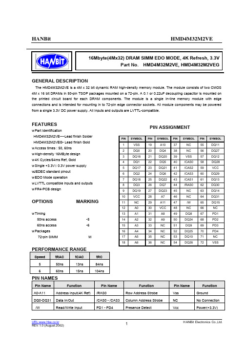
HANBit HMD4M32M2VEGENERAL DESCRIPTIONThe HMD4M32M2VE is a 4M x 32 bit dynamic RAM high-density memory module. The module consists of two CMOS 4M x 16 bit DRAMs in 50-pin TSOP packages mounted on a 72-pin. A 0.1 or 0.22uF decoupling capacitor is mounted on the printed circuit board for each DRAM components. The module is a single In-line memory module with edge connections and is intended for mounting in to 72-pin edge connector sockets. All module components may be powered from a single 3.3V DC power supply. All inputs and outputs are LVTTL-compatible.FEATURESw Part IdentificationHMD4M32M2VE----Lead finish Solder HMD4M32M2VEG- Lead finish Gold w Access times : 50, 60ns w High-density 16MByte design w 4K Cycles/64ms Ref, Gold w Single +3.3V ± 0.3V power supply w JEDEC standard pinout w EDO Mode operationw LVTTL compatible inputs and outputs w FR4-PCB designOPTIONS MARKINGw Timing50ns access -5 60ns access -6 w Packages72-pin SIMM MPERFORMANCE RANGESpeed tRAC tCAC tRC 5 50ns 13ns 84ns 660ns15ns104nsPIN NAMESPin Name FunctionPin Name FunctionPin Name Function A0-A11 Address Input(4K Ref) /RAS0 Row Address Strobe Vss Ground DQ0-DQ31 Data In/Out /CAS0 - /CAS3 Column Address Strobe NC No Connection /W Read/Write InputPD1 - PD4Presence DetectVccPower(+3.3V)PIN ASSIGNMENTPINSYMBOLPINSYMBOLPINSYMBOLPINSYMBOL1 VSS 19 A10 37 NC 55 DQ112 DQ0 20 DQ4 38 NC 56 DQ273 DQ16 21 DQ20 39 VSS 57 DQ124 DQ1 22 DQ5 40 /CAS0 58 DQ28 5 DQ17 23 DQ21 41 /CAS2 59 VCC6 DQ2 24 DQ6 42 /CAS3 60 DQ297 DQ18 25 DQ22 43 /CAS1 61 DQ13 8 DQ3 26 DQ7 44 /RAS0 62 DQ309 DQ19 27 DQ23 45 NC 63 DQ14 10 VCC 28 A7 46 NC 64 DQ31 11 NC 29 A11 47 /W 65 DQ15 12 A0 30 VCC 48 NC 66 NC 13 A1 31 A8 49 DQ8 67 PD1 14 A2 32 A9 50 DQ24 68 PD2 15 A3 33 NC 51 DQ9 69 PD3 16A4 34 NC 52 DQ25 70 PD4 17 A5 35 NC 53 DQ10 71 NC 18A636NC54DQ2672VSSHANBit HMD4M32M2VEFUNCTIONAL BLOCK DIAGRAMToall DRAMs0.1uF or 0.22uFCapacitorfor each DRAMDQ0-DQ7DQ8-DQ15DQ16-DQ23DQ24-DQ31/RAS0/CAS0/CAS1/CAS2/CAS3/WA0-A11Vcc VssHANBit HMD4M32M2VE ABSOLUTE MAXIMUM RATINGSPARAMETER SYMBOL RATINGVoltage on Any Pin Relative to Vss V IN ,OUT-0.5V to 6.5VVoltage on Vcc Supply Relative to Vss Vcc -0.5V to 4.6VPower Dissipation P D2WStorage Temperature T STG-55o C to 150o CShort Circuit Output Current I OS50mAw Permanent device damage may occur if " Absolute Maximum Ratings" are exceeded. Functional operation should be restricted to the conditions as detailed in the operational sections of this data sheet. Exposure to absolute maximum rating conditions for extended periods may affect device reliability.RECOMMENDED DC OPERATING CONDITIONS( Voltage reference to V SS, T A=0 to 70 o C )PARAMETER SYMBOL MIN TYP. MAX UNIT Supply Voltage Vcc 3.0 3.3 3.6 V Ground Vss 0 0 0 V Input High Voltage V IH 2.0 - +5.5 V Input Low Voltage V IL-0.3 - 0.8 VDC AND OPERATING CHARACTERISTICSSYMBOL SPEED MIN MAX UNITS-5 - 220 mAI CC1-6 - 200 mAI CC2- 4 mA-5 - 220 mAI CC3-6 - 200 mA-5 - 220 mAI CC4-6 - 200 mAI CC5- 600 mA-5 - 220 mAI CC6-6 - 200 mAI l(L)-10 10 µAI O(L)-10 10 µAV OH 2.4 - VV OL- 0.4 VI CC1 : Operating Current * (/RAS , /CAS , Address cycling @t RC=min.)I CC2 : Standby Current ( /RAS=/CAS=V IH )HANBit HMD4M32M2VEI CC3 : /RAS Only Refresh Current * (/CAS=V IH, /RAS, Address cycling @t RC=min )I CC4 : Fast Page Mode Current * (/RAS=V IL, /CAS, Address cycling @t PC=min )I CC5 : Standby Current (/RAS=/CAS=Vcc-0.2V )I CC6 : /CAS-Before-/RAS Refresh Current * (/RAS and /CAS cycling @t RC=min )* NOTE: I CC1, I CC3, I CC4 and I CC6 are dependent on output loading and cycle rates. Specified values are obtained with the output open. I CC is specified as an average current. In I CC1 and I CC3, address cad be changed maximum once while /RAS=V IL. In I CC4, address can be changed maximum once within one page mode cycle.CAPACITANCE( TA =25oC, Vcc = 3.3V, f = 1Mz )DESCRIPTION SYMBOL MIN MAX UNITS Input Capacitance (A0-A11) C IN1- 10 pF Input Capacitance (/W) C IN2- 14 pF Input Capacitance (/RAS0, /RAS1) C IN3- 14 pF Input Capacitance (/CAS0-/CAS3) C IN4- 14 pF Input/Output Capacitance (DQ0-31) C DQ1- 14 pFAC CHARACTERISTICS( 0 o C ≤ TA≤ 70o C , Vcc = 3.3V±10%, See notes 1,2.)-5 -6STANDARD OPERATION SYMBOLMIN MAX MIN MAXUNIT Random read or write cycle time t RC84 104 ns Access time from /RAS t RAC50 60 ns Access time from /CAS t CAC13 15 ns Access time from column address t AA25 30 ns /CAS to output in Low-Z t CLZ 3 3 ns Transition time (rise and fall) t T 1 50 1 50 ns /RAS precharge time t RP30 40 ns /RAS pulse width t RAS50 10K 60 10K ns /RAS hold time t RSH13 15 ns /CAS hold time t CSH38 45 ns /CAS pulse width t CAS8 10K 10 10K ns /RAS to /CAS delay time t RCD20 37 20 45 ns /RAS to column address delay time t RAD15 25 15 30 ns /CAS to /RAS precharge time t CRP 5 5 ns Row address set-up time t ASR0 0 ns Row address hold time t RAH10 10 ns Column address set-up time t ASC0 0 nsHANBit HMD4M32M2VEColumn address hold time t CAH8 10 ns Column Address to /RAS lead time t RAL25 30 ns Read command set-up time t RCS0 0 ns Read command hold referenced to /CAS t RCH0 0 ns Read command hold referenced to /RAS t RRH0 0 ns Write command hold time t WCH10 10 ns Write command pulse width t WP10 10 ns Write command to /RAS lead time t RWL10 10 ns Write command to /CAS lead time t CWL8 10 ns Data-in set-up time t DS0 0 ns Data-in hold time t DH8 10 ns Refresh period t REF64 64 ns Write command set-up time t WCS0 0 ns /CAS setup time (C-B-R refresh) t CSR 5 5 ns /CAS hold time (C-B-R refresh) t CHR10 10 ns /RAS precharge to /CAS hold time t RPC 5 5 ns Access time from /CAS precharge t CPA35 40 ns Fast page mode cycle time t PC28 35 ns /CAS precharge time (Fast page) t CP8 10 ns /RAS pulse width (Fast page ) t RASP50 100K 60 100K ns /W to /RAS precharge time (C-B-R refresh) t WRP10 10 ns /W to /RAS hold time (C-B-R refresh) t WRH10 10 ns NOTES1.An initial pause of 200µs is required after power-up followed by any 8 /RAS-only or /CAS-before-/RAS refresh cycles before proper device operation is achieved.2.V IH (min) and V IL (max) are reference levels for measuring timing of input signals. Transition times are measured between V IH(min) and V IL(max) and are assumed to be 5ns for all inputs.3.Measured with a load equivalent to 1TTL loads and 100pF4.Operation within the t RCD(max) limit insures that t RAC(max) can be met. t RCD(max) is specified as a reference point only. If t RCD is greater than the specified t RCD(max) limit, then access time is controlled exclusively by t CAC.5.Assumes that t RCD≥ t RCD(max)6. t AR, t WCR, t DHR are referenced to t RAD(max)7.This parameter defines the time at which the output achieves the open circuit condition and is not referenced to V OHor V OL.8. t WCS, t RWD, t CWD and t AWD are non restrictive operating parameter.They are included in the data sheet as electrical characteristic only. If t WCS≥tWCS(min) the cycle is an early writecycle and the data out pin will remain high impedance for the duration of the cycle.9. Either t RCH or t RRH must be satisfied for a read cycle.10. These parameters are referenced to the /CAS leading edge in early write cycles and to the /W leading edge in read-write cycles.11. Operation within the t RAD(max) limit insures that t RAC(max) can be met. t RAD(max) is specified as a referencepoint only. If t RAD is greater than the specified t RAD(max) limit. then access time is controlled by t AA.HANBit HMD4M32M2VE TIMING DIAGRAMPlease refer to attached timing diagram chart (I)PACKAGING INFORMATIONSIMM DesignORDERING INFORMATIONPart Number Density Org. Package RefreshCycleVcc SPEEDHMD4M32M2VEG-5 16MByte 4MX 32bit 72 Pin-SIMM 4,096 Cycles64ms Ref.3.3V 50nsHMD4M32M2VEG-6 16MByte 4MX 32bit72 Pin-SIMM 4,096 Cycles64ms Ref.3.3V 60ns19.000.25 mm MAX。
3232E中文资料
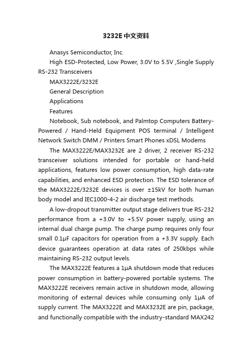
3232E中文资料Anasys Semiconductor, Inc.High ESD-Protected, Low Power, 3.0V to 5.5V ,Single Supply RS-232 TransceiversMAX3222E/3232EGeneral DescriptionApplicationsFeaturesNotebook, Sub notebook, and Palmtop Computers Battery-Powered / Hand-Held Equipment POS terminal / Intelligent Network Switch DMM / Printers Smart Phones xDSL Modems The MAX3222E/MAX3232E are 2 driver, 2 receiver RS-232 transceiver solutions intended for portable or hand-held applications, features low power consumption, high data-rate capabilities, and enhanced ESD protection. The ESD tolerance of the MAX3222E/3232E devices is over ±15kV for both human body model and IEC1000-4-2 air discharge test methods.A low-dropout transmitter output stage delivers true RS-232 performance from a +3.0V to +5.5V power supply, using an internal dual charge pump. The charge pump requires only four small 0.1μF capacitors for operation from a +3.3V supply. Each device guarantees operation at data rates of 250kbps while maintaining RS-232 output levels.The MAX3222E features a 1μA shutdown mode that reduces power consumption in battery-powered portable systems. The MAX3222E receivers remain active in shutdown mode, allowing monitoring o f external devices while consuming only 1μA of supply current. The MAX3222E and MAX3232E are pin, package, and functionally compatible with the industry-standard MAX242and MAX232, respectively.Meets true EIA/TIA-232-F Standards from a +3.0V to +5.5V power supply Interoperable with EIA/TIA - 232 and adheres to EIA/TIA - 562 1μA Low-Power Shutdown (MAX3222E) Enhanced ESD Specifications:15kV Human Body Model 15kV IEC1000-4-2 Air Discharge 8kV IEC1000-4-2 Contact Discharge 250 kbps Minimum Transmission RateIdeal for Handheld, Battery Operated Applications Latch up FreeGuaranteed 30V/μs Max Slew Rate BiCMOS TechnologyOrdering InformationAbsolute Maximum RatingsStresses beyond those listed under Absolute Maximum Ratings may cause permanent damage to the device. These are stress ratings only, and functional operation of the device at these or any other conditions beyond those indicated in the operational sections of the specifications is not implied. Exposure to absolute maximum rating conditions for extended periods may affect device reliability.Pin DescriptionElectrical Characteristics(VCC = +3V to +5.5V, C1-C4 = 0.1μF, T A = T MIN to T MAX, unless otherwise noted. Typical values are at T A = +25°C.)Typical Operating CharacteristicsAnasys Semiconductor, Inc.(VCC = +3.3V, 250kbps data rate, 0.1μF capacitors, all transmitters loaded with 3k ? and CL, TA = +25°C, unless otherwise noted.)T1 TRANSMITTING AT 250kbps T2 TRANSMITTING AT 15.6kbpsTypical Operating CircuitsC 3C 4Detailed DescriptionAnasys Semiconductor, Inc.Dual Charge-Pump Voltage ConverterThe MAX3222E/MAX3232Es’ internal power supply consists of a regulated dual charge pump that provides output voltages of +5.5V (doubling charge pump) and -5.5V (inverting charge pump) over the +3.0V to +5.5V VCC range. The charge pump operates in discontinuous mode; if the output voltages are less than 5.5V, the charge pump is enabled, and if the outputvoltages exceed 5.5V, the charge pump is disabled. Each charge pump requires a flying capacitor (C1, C2) and a storage capacitor (C3, C4) to generate the V+ and V- supplies. RS-232 Transmitters The transmitters are inverting level translators that convert TTL/CMOS-logic levels to ±5V EIA/TIA-232 compliant levels. The MAX3222E/MAX3232E transmitters guarantee a 250kbps data rate with worst-case loads of 3K Ω parallel with 1000pF. Transmitters can be paralleled to drive multiple receivers. The MAX3222E transmitters are disabled and the outputs are forced into ahigh-impedance state when the device is in shutdown mode (SHDN =GND). The MAX3222E/MAX3232E permits the outputs to be driven up to ±12V in shutdown. RS-232 ReceiversThe receivers convert RS-232 signals to CMOS-logic output levels. The MAX3222E receivers have inverting three-state outputs. Drive EN high to place the receiver(s) into a high impedance state. Receivers can be either active or inactive in shutdown. MAX3222ESupply current falls to less than 1μA in shutdown mode (= GND). When shutdown, the device’s charge pumps are shut off, V+ is pulled down to VCC, V- is pulled to ground, and the transmitter outputs are disabled (high impedance). The time required to recov er from shutdown is typically 100μs. Connect SHDN to VCC if shutdown mode is not used. ±15kV ESD ProtectionESD-protection structures are incorporated to protect against electrostatic discharges encountered during handling and assembly. The driver outputs and receiver inputs of the MAX3222E/MAX3232E have extra protection against staticelectricity. The ESD structures withstand high ESD in all states:normal operation, shutdown, and powered down. After an ESD event, Circuits keep working without latch up. ESD protection can be tested in various ways; the transmitter outputs and receiver inputs for the MAX3222E/MAX3232E are characterized for protection to the following limits: ? ±15kV using the Human Body Model±8kV using the Contact Discharge method specified in IEC 1000-4-2 ? ±15kV using the Air-Gap Discharge method specified in IEC 1000-4-2Anasys Semiconductor, Inc.Application InformationCapacitor SelectionThe capacitor type used for C1–C4 is not critical for proper operation; polarized or non-polarized capacitors can be used. The charge pump requires 0.1μF capacitors for 3.3V operation. Increasing the capacitor values (e.g., by a factor of 2) reduces ripple on the transmitter outputs and slightly reduces power consumption. C2, C3, and C4 can be increased without changing C1’s value. When using the minimum required capacitor values, make sure the capacitor value does not degrade excessively with temperature. If in doubt, use capacitors with a larger nominal value. The capacitor’s equivalent series resistanc e (ESR), which usually rises at low temperatures, influences the amount of ripple on V+ and V- output voltages.Power-Supply DecouplingIn most circumstances, a 0.1μF VCC bypass capacitor is adequate. In applications sensitive to power-supply noise, use a capacitor of the same value as charge pump capacitor C1. Connect bypass capacitors as close to the IC as possible.Operation Down to 2.7VTransmitter outputs meet EIA/TIA-562 levels of ±3.7V with supply voltages as low as 2.7V. Transmitter Outputs Recovering from ShutdownWhen MAX3222E’s two transmitter outputs were recovering from shutdown mode, the two transmitter outputs are shown going to opposite RS-232 levels (one transmitter input is high; the other is low) as they become active. Each transmitter is loaded with 3K resistor in parallel with 2500pF. The transmitter outputs display no ringing or undesirable transients as they come out of shutdown. Note that the transmitters are enabled only when the magnitude of V- exceeds approximately -3.0V. Interconnection with 3V and 5V LogicThe MAX3222E/MAX3232E can directly interface with various 3V and 5V logic families, including ACT and HCT CMOS.。
电梯控制器

种类
编辑
直流电动机具有调速性能好、调速范围大的特点,因此很早就应用于电梯上,采用发电机一电动机组形式驱 动。它控制的电梯速度达4m/s,但是,机组结构体积大、耗电大、维护工作量较大、造价高,因此常用于对速度, 舒适感要求较高的建筑物中。
电梯控制柜可控硅直接供电系统在工业上早有应用,但用于电梯上却要解决舒适感,尤其是低速段问题,因 此应用较晚,它几乎与微机同时应用。比起电动机一发电机组形式的直流电梯,它有很多优点,如机房占地节省 35%、重量减轻40%、节能25%-35%。世界上最高速度的10m/s电梯就是采用这种系统,其调速比达1:1200。
性能参数
卡容量:20000张 记录存量:60000条 报警容量:10000条 通讯方式:485 通讯距离:1200米(实际工程应用控制在800米以内为宜) 读卡器通讯:wiegand(韦根)方式 通讯距离:100米以内 开门方式:卡、密码、卡+密码、双卡、首卡开门、软件、火警、按钮、定时
电梯管理软件
常用的机种如下:手柄开关定向,井道分层转换开关定向,井道永磁开关与继电器组成的逻辑电路定向,机 械选层器定向,双稳态磁开关和电子数字电路定向,电子脉冲式选层装置定。
电梯的定向,选层线路 :电梯的方向控制就是根据电梯轿厢内乘客的目的层站指令和各层楼召唤信号与电梯 所处层楼位置信号进行比较,凡是在电梯位置信号上方的轿厢内指令和层站召唤信号,令电梯定上行,反之定下 行。方向控制环节必须注意以下几点:
具有消防信号输入接口,当无源的干接点消防开关信号启动后,IC卡电梯系统不工作,电梯恢复到原状态; 使用低功率之CMOS微电脑、断电时人员及储存资料可保存10年绝不流失;含高级接待卡功能;脱机或者联网状态系 统会自动记录每次成功刷卡使用电梯的相关信息,包括使用者卡号、使用时间、所使用的电梯代号、所到达的楼 层以及交易情况等信息,以作统计、打印、存档、查询.
海视群-4 MP 32× IR 网络速度球机 DS-2DE7A432IW-AEB(T5)说明书
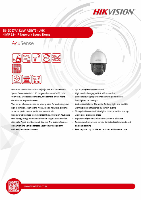
DS-2DE7A432IW-AEB(T5)-UHK 4 MP 32× IR Network Speed DomeHikvision DS-2DE7A432IW-AEB(T5) 4 MP 32× IR Network Speed Dome adopts 1/1.8" progressive scan CMOS chip. With the 32× optical zoom lens, the camera offers more details over expansive areas.This series of cameras can be widely used for wide ranges of high-definition, such as the rivers, roads, railways, airports, squares, parks, scenic spots, and venues, etc.Empowered by deep learning algorithms, Hikvision AcuSense technology brings human and vehicle targets classification alarms to front- and back-end devices. The system focuses on human and vehicle targets, vastly improving alarm efficiency and effectiveness.⏹ 1/1.8" progressive scan CMOS⏹ High quality imaging with 4 MP resolution ⏹Excellent low-light performance with powered-by-DarkFighter technology⏹Audio visual alarm: The white flashing light and audible warning can be triggered by certain events ⏹32× optical zoom and 16× digital zoom provide close up views over expansive areas⏹ Expansive night view with up to 200 m IR distance ⏹Focuses on human and vehicle targets classification based on deep learning⏹ Face capture: Up to 5 faces captured at the same time⏹DORIThe DORI (detect, observe, recognize, identify) distance gives the general idea of the camera ability to distinguish persons or objects within its field of view. It is calculated based on the camera sensor specification and the criteria given by EN 62676-4: 2015.DORI Detect Observe Recognize IdentifyDefinition25 px/m63 px/m125 px/m250 px/mDistance (Tele)2046.9 m (6715.5 ft)812.3 m (2665.0 ft) 409.4 m (1343.2 ft)204.7 m (671.6 ft)⏹SpecificationCameraMax. Resolution 2560 × 1440Image Sensor 1/1.8" progressive scan CMOSMin. Illumination Color: 0.005 Lux @ (F1.5, AGC ON), B/W: 0.001 Lux@(F1.5, AGC ON), 0 Lux with IR Shutter Speed 1/1 s to 1/30000 sSlow Shutter YesDay & Night IR cut filterZoom 32x optical, 16x digitalLensFocal Length 4.5 mm to 188 mmZoom Speed Approx. 4.8 sFOV Horizontal field of view: 50.8° to 2.6° (wide-tele), Vertical field of view: 29.4° to 1.5° (wide-tele), Diagonal field of view:57.4° to 3° (wide-tele)Aperture Max. F1.4 ~ F2.6Focus Auto, semi-auto, manual, rapid focus, close focus distance 100mm ~ 1000mm or more IlluminatorSupplement Light Type IRSupplement Light Range IR Distance: up to 200 mPTZMovement Range (Pan) 360°Movement Range (Tilt) -15° to 90° (auto flip)Pan Speed Pan speed: configurable from 0.1° to 160°/s; preset speed: 240°/sTilt Speed Tilt speed: configurable from 0.1° to 120°/s, preset speed 200°/sProportional Pan YesPresets 300Patrol Scan 8 patrols, up to 32 presets for each patrolPattern Scan 4 pattern scansPower-off Memory YesPark Action Preset, pattern scan, auto scan, tilt scan, random scan, frame scan, panorama scan3D Positioning YesPTZ Status Display YesPreset Freezing YesScheduled Task Preset, pattern scan, patrol scan, auto scan, tilt scan, random scan, frame scan, panorama scan, dome reboot, dome adjust, aux outputVideoMain Stream 50 Hz: 25 fps (2560 × 1440, 1920 × 1080, 1280 × 960, 1280 × 720);60 Hz: 24 fps (2560 × 1440, 1920 × 1080, 1280 × 960, 1280 × 720)Sub-Stream 50 Hz: 25 fps (704 × 576, 640 × 480, 352 × 288);60 Hz: 24 fps (704 × 480, 640 × 480, 352 × 240)Third Stream 50 Hz: 25 fps (1920 × 1080, 1280 × 960, 1280 × 720, 704 × 576, 640 × 480, 352 × 288);60 Hz: 24 fps (1920 × 1080, 1280 × 960, 1280 × 720, 704 × 480, 640 × 480, 352 × 240)Video Compression Main stream: H.265+/H.265/H.264+/H.264 Sub-stream: H.265/H.264/MJPEGThird stream: H.265/H.264/MJPEGVideo Bit Rate 32 kbps to 16384 kbpsH.264 Type Baseline Profile/Main Profile/High ProfileH.265 Type Main ProfileScalable Video Coding (SVC) H.264 and H.265 encodingRegion of Interest (ROI) 8 fixed regions for each streamAudioAudio Compression G.711alaw, G.711ulaw, G.722.1, G.726, MP2L2, AAC, PCMAudio Bit Rate 64 Kbps (G.711)/16 Kbps (G.722.1)/16 Kbps (G.726)/32-192 Kbps (MP2L2)/16-64 Kbps (AAC)Audio Sampling Rate 8 kHz/16 kHz/32 kHz/48 kHzEnvironment Noise Filtering YesNetworkNetwork Storage NAS (NFS, SMB/CIFS), auto network replenishment (ANR)Protocols IPv4/IPv6, HTTP, HTTPS, 802.1x, QoS, FTP, SMTP, ARP, UPnP, SNMP, DNS, DDNS, NTP, RTSP, RTCP, RTP, TCP/IP, UDP, IGMP, ICMP, DHCP, SSL, PPPoE, Bonjour, Websocket, WebsocketsAPI Open Network Video Interface (Version 19.12, Profile S, Profile G, Profile T), ISAPI, SDK, ISUPSimultaneous Live View Up to 20 channelsUser/Host Up to 32 users, 3 user levels: administrator, operator, and userSecurity Password protection, complicated password, HTTPS encryption, 802.1X authentication (EAP-TLS, EAP-LEAP, EAP-MD5), watermark, IP address filter, basic and digest authentication for HTTP/HTTPS, RTP/RTSP over HTTPS, control timeout settings, security audit log, TLS 1.2, TLS 1.3, host authentication (MAC address)Client iVMS-4200, HikCentral Pro, Hik-Connect Web Browser IE11, Chrome 57+, Firefox 52+, Safari 11+ ImageDay/Night Switch Day, Night, Auto, ScheduleImage Enhancement BLC, HLC, 3D DNR, DWDRWide Dynamic Range (WDR) 120 dBDefog Digital defogImage Stabilization EISRegional Exposure YesRegional Focus YesImage Settings Saturation, brightness, contrast, sharpness, gain, and white balance adjustable by client software or web browserPrivacy Mask 24 programmable polygon privacy masks, mask color or mosaic configurable SNR > 52 dBInterfaceEthernet Interface 1 RJ45 10M/100M self-adaptive Ethernet portOn-board Storage Built-in memory card slot, support microSD/SDHC/SDXC card, up to 256 GB Alarm 2 inputs, 1 outputAudio 1 input (line in), max. input amplitude: 2-2.4 vpp, input impedance: 1 kΩ ± 10%;1 output (line out), line level, output impedance: 600 ΩReset YesBuilt-in Speaker 1 built-in speaker with effective distance reaching max. 30 metersEventBasic Event Motion detection, video tampering alarm, exception, alarm input and outputSmart Event Line crossing detection, intrusion detection, region entrance detection, region exiting detection, unattended baggage detection, object removal detection, audio exception detectionSmart Tracking Manual tracking, auto-trackingAlarm Linkage Upload to FTP/NAS/memory card, notify surveillance center, send email, trigger alarm output, trigger recording, audible warning, white light flashing, and PTZ actions (such as preset, patrol scan, pattern scan)Deep Learning FunctionFace Capture Detects up to 5 faces simultaneously.Supports detecting, capturing, grading, selecting of face in motion, and output the best face picture of the facePerimeter Protection Line crossing, intrusion, region entrance, region exitingSupport alarm triggering by specified target types (human and vehicle)GeneralPower 24 VAC, max. 42 W (including max. 18 W for IR and max. 10 W for heater); Hi-PoEOperating Condition -30 °C to 65 °C (-22 °F to 149 °F). Humidity 90% or less (non-condensing) Demist YesMaterial ADC12Dimension Ø 220 mm × 363.3 mm (Ø 8.66" × 13.91")Weight Approx. 5 kg (11.03 lb.)ApprovalProtection IP67 (IEC 60529-2013), IK10 (excluding glass window), TVS 6000V lightning protection, surge protection and voltage transient protectionEMC FCC SDoC (47 CFR Part 15, Subpart B);CE-EMC (EN 55032: 2015, EN 61000-3-2: 2019, EN 61000-3-3: 2013, EN 50130-4: 2011 +A1: 2014);RCM (AS/NZS CISPR 32: 2015);IC VoC (ICES-003: Issue 6, 2019);KC (KN 32: 2015, KN 35: 2015)SafetyUL (UL 62368-1);CB (IEC 60950-1:2005 + Am 1:2009 + Am 2:2013, IEC 62368-1:2014);CE-LVD (EN 62368-1:2014+A11:2017); BIS (IS 13252(Part 1):2010+A1:2013+A2:2015); LOA (SANS IEC60950-1)EnvironmentCE-RoHS (2011/65/EU); WEEE (2012/19/EU); Reach (Regulation (EC) No 1907/2006)⏹Typical ApplicationHikvision products are classified into three levels according to their anti-corrosion performance. Refer to the following description to choose for your using environment.This model has NO SPECIFIC PROTECTION.LevelDescriptionTop-level protectionHikvision products at this level are equipped for use in areas where professional anti-corrosion protection is a must. Typical application scenarios include coastlines, docks, chemical plants, and more.Moderate protectionHikvision products at this level are equipped for use in areas with moderate anti-corrosion demands. Typical application scenarios include coastal areas about 2 kilometers (1.24 miles) away from coastlines, as well as areas affected by acid rain.No specific protectionHikvision products at this level are equipped for use in areas where no specific anti-corrosion protection is needed.⏹Available Model DS-2DE7A432IW-AEB(T5)⏹Dimension⏹Accessory⏹IncludedDS-1602ZJWall mount⏹OptionalDS-1619ZJ DS-1662ZJ DS-1660ZJ DS-1661ZJ DS-1673ZJDS-1604ZJ-BOX-CORNER DS-1604ZJ-boxDS-1604ZJ-BOX-POLEDS-1681ZJ DS-1682ZJDS-1667ZJ DS-1663ZJ DS-1604ZJ*DS-1673ZJ should be used with DS-1661ZJ or DS-1662ZJ.。
长斯系电子 FORESEE eMMC FEMDNN032G-58A46 数据手册说明书
FORESEE eMMC FEMDNN032G-58A46DatasheetE-00873Version: 1.02021.10.09LONGSYS ELECTRONICS RESERVES THE RIGHT TO CHANGE PRODUCTS, INFORMATION AND SPECIFICATIONS WITHOUT NOTICE.Products and specifications discussed herein are for reference purposes only. All information discussed herein is provided on an “AS IS” basis, without warranties of any kind.This document and all information discussed herein remain the sole and exclusive property of Longsys Electronics. No license of any patent, copyright, mask work, trademark or any other intellectual property right is granted by one party to the other party under this document, by implication, estoppel or other-wise.Longsys products are not intended for use in life support, critical care, medical, safety equipment, or similar applications where product failure could result in loss of life or personal or physical harm, or any military or defense application, or any governmental procurement to which special terms or provisions may apply.For updates or additional information about Longsys products, contact your nearest Longsys office.All brand names, trademarks and registered trademarks belong to their respective owners.ⓒ 2021 Shenzhen Longsys Electronics Co., Ltd. All rights reserved.CONTENTS1.Introduction (4)2. Product List (4)3. Features (4)4. Functional Description (5)5. Product Specifications (6)5.1 Performance (6)5.2 Power Consumption (6)6. Pin Assignments (7)6.1 Ball Array view (7)6.2 Ball Array view (8)7. Usage Overview (9)7.1 General description (9)7.2 Partition Management (9)7.3 Automatic Sleep Mode (11)7.4 Sleep (CMD5) (11)7.5 H/W Reset operation (12)7.6 High-speed mode selection (12)7.7 Bus width selection (12)7.8 Partition configuration (12)7.9 CID register (12)7.10 CSD register (13)7.11 Extended CSD register (14)7.12 OCR Register (23)7.13 Field firmware update(FFU) (23)7.14 S.M.A.R.T. Health Report (25)8. Package Dimension (26)9 Connection Guide (26)9.1 Schematic Diagram (26)10. Processing Guide (27)1.IntroductionISOCOM eMMC is an embedded storage solution designed in the BGA package. The ISOCOM eMMC consists of NAND flash and eMMC controller. The controller could manage the interface protocols,wear-leveling,bad block management and ECC.ISOCOM eMMC has high performance at a competitive cost, high quality and low power consumption, and eMMC is compatible with JEDEC standard eMMC 5.1 specifications.3. Features➢eMMC5.1 specification compatibility (Backward compatible to eMMC4.41/4.5/5.0)➢Bus mode- Data bus width: 1 bit (default), 4 bits, 8 bits- Data transfer rate: up to 400MB/s (HS400)- MMC I/F Clock frequency : 0~200MHz➢Operating voltage range- Vcc(NAND) : 2.7 - 3.6V- Vccq(Controller) : 1.7 - 1.95V / 2.7 - 3.6V➢Temperature- Operation (-25℃~ +85℃)- Storage without operation (-40℃~ +85℃)➢Sudden-Power-Loss safeguard➢Hardware ECC engine➢Unique firmware backup mechanism ➢Global-wear-leveling➢Supported features.-HS400, HS200-Partitioning, RPMB-Boot feature, boot partition-HW Reset/SW Reset-Discard, Trim, Erase, Sanitize-Background operations, HPI-Enhanced reliable write-S.M.A.R.T. Health Report-FFU-Sleep / awake➢Others- Compliance with the RoHS Directive4. Functional DescriptionISOCOM eMMC with powerful L2P (Logical to Physical) NAND Flash management algorithm provides unique functions:➢Host independence from details of operating NAND flash➢Internal ECC to correct defect in NAND flash➢Sudden-Power-Loss safeguardTo prevent from data loss, a mechanism named Sudden-Power-Loss safeguard is added in the eMMC. In the case of sudden power-failure, the eMMC would work properly after power cycling.➢Global-wear-levelingTo achieve the best stability and device endurance, this eMMC equips the Global Wear Leveling algorithm. It ensures that not only normal area, but also the frequently accessed area, such as FAT, would be programmed and erased evenly.➢IDA(Initial Data Acceleration)The eMMC prevents the pre-burned data from data-loss with IDA, in case of our customer had pre-burned data to eMMC, before the eMMC being SMT.➢CacheThe eMMC enhanced the data written performance with Cache, with which our customer would get more endurance and reliability.5. Product Specifications• Test Condition: Bus width x8, 200MHz DDR, 512KB data transfer, w/o file system overhead, measured on internal board • Test tool: uBOOT (Without O/S)• Chunk size: 1MB,• Test area: 100MB/ Full-range of LBA.5.2 Power Consumption5.2.1 Active power consumption during operation• Power Measurement conditions: Bus configuration =x8 @200MHz DDR, 25℃.• Vcc:3.3V & Vccq:1.8V.• The measurement for max RMS current is the average RMS current consumption over a period of 100ms.5.2.2 Low power mode (stand-by)• Power Measurement conditions: Bus configuration =x8 @200MHz DDR, 25℃.• Standby: Nand Vcc & Controller Vccq power supply is switched on.• The measurement for max RMS current is the average RMS current consumption over a period of 100ms.5.2.3 Low power mode (sleep)• Power Measurement conditions: Bus configuration =x8 @200MHz DDR, 25℃.• Sleep: Nand Vcc power supply is switched off(Controller Vccq on)• The measurement for max RMS current is the average RMS current consumption over a period of 100ms.6. Pin Assignments6.1 Ball Array viewFBGA153 - Ball Array (Top view(ball site down))Note:NC: No Connect, shall be connected to ground or left floating. RFU: Reserved for Future Use, must be left floating for future use. VSF: Vendor Specific Function, must be left floating.7.1 General descriptionThe eMMC can be operated in 1, 4, or 8-bit mode. NAND flash memory is managed by a controller inside, which manages ECC, wear leveling and bad block management. The eMMC provides easy integration with the host process that all flash management hassles are invisible to the host.7.2 Partition ManagementThe embedded device offers also the possibility of configuring by the host additional split local memory partitions with independent addressable space starting from logical address 0x00000000 for different usage models. Default size of each Boot Area Partition is 4096 KB and can be changed by Vendor Command as multiple of 128KB. Boot area partition size is calculated as ( 128KB * BOOT_SIZE_MUL TI ) The size of Boot Area Partition 1 and 2 cannot be set independently and is set as same value Boot area partition which is enhanced partition. Therefore memory block area scan is classified as follows:➢Factory configuration supplies boot partitions.➢The RPMB partition is 4MB.➢The host is free to configure one segment in the User Data Area to be implemented as enhanced storage media, and to specify its starting location and size in terms of Write Protect Groups. The attributes of this Enhanced User Data Area can be programmed only once during the device life-cycle (one-time programmable).➢Up to four General Purpose Area Partitions can be configured to store user data or sensitive data, or for other host usage models. The size of these partitions is a multiple of the write protect group. Size and attributes can be programmed once in device life-cycle (one-time programmable). Each of the General Purpose Area Partitions can be implemented with enhanced technological features.Partitions and user data area configuration(The size of RPMB area partition is 4MB)In boot operation mode, the master can read boot data from the slave (device) by keeping CMD line low or sending CMD0 with argument + 0xFFFFFFFA, before issuing CMD1. The data can be read from either boot area or user area dependingState diagram (boot mode)State diagram (alternative boot mode)State diagram (boot mode)*7.3 Automatic Sleep ModeIf host does not issue any command during certain duration (1s), after previously issued command is completed, the device enters “Power Saving mode” to reduce power consumption. At this time, commands arriving at the device while it is in power saving mode will be serviced in normal fashion. The below table explains the condition to enter and exit Auto Power Saving Mode7.4 Sleep (CMD5)A card may be switched between a Sleep state and a Standby state by SLEEP/AWAKE (CMD5). In the Sleep state the power consumption of the memory device is minimized. In this state the memory device reacts only to the commands RESET (CMD0 with argument of either 0x00000000 or 0xF0F0F0F0 or H/W reset) and SLEEP/AWAKE (CMD5). All the other commands are ignored by the memory device. The timeout for state transitions between Standby state and Sleep state is defined in the EXT_CSD register S_A_timeout. The maximum current consumptions during the Sleep state are defined in the EXT_CSD registers S_A_VCC and S_A_VCCQ. Sleep command: The bit 15 as set to 1 in SLEEP/ AWAKE (CMD5) argument. A wake command: The bit 15 as set to 0 in SLEEP/AWAKE (CMD5) argument.7.5 H/W Reset operationDevice will detect the rising edge of RST_n signal to trigger internal reset sequenceH/W reset waveform7.6 High-speed mode selectionAfter the host verifies that the card complies with version 4.0, or higher, of this standard, it has to enable the high speed mode timing in the card, before changing the clock frequency to a frequency higher than 20MHz. For the host to change to a higher clock frequency, it has to enable the high speed interface timing. The host uses the SWITCH command to write 0x01 to the HS_TIMING byte, in the Modes segment of the EXT_CSD register.7.7 Bus width selectionAfter the host has verified the functional pins on the bus it should change the bus width configuration accordingly, using the SWITCH command. The bus width configuration is changed by writing to the BUS_WIDTH byte in the Modes Segment of the EXT_CSD register (using the SWITCH command to do so). After power-on, or software reset, the contents of the BUS_WIDTH byte is 0x00.7.9 CID registerThe Card Identification (CID) register is 128 bits wide. It contains the card identification information used during the card identification phase (protocol). Every individual flash or I/O card shall have an unique identification number. Every type of ROM cards (defined by content) shall have a unique identification number. The structure of the CID register is defined7.10 CSD registerThe Card-Specific Data (CSD) register provides information on how to access the card contents. The CSD defines the data format, error correction type, maximum data access time, data transfer speed, whether the DSR register can be used etc. The programmable part of the register (entries marked by W or E, see below) can be changed by CMD27. The type of the CSD Registry entries coded as follows:7.11 Extended CSD registerThe Extended CSD register defines the card properties and selected modes. It is 512 bytes long. The most significant 320 bytes are the Properties segment, which defines the card capabilities and cannot be modified by the host. The lower 192 bytes are the Modes segment, which defines the configuration the card is working in. These modes can be changed by the host by means of the SWITCH command.Notes: 1.R= Read-onlyR/W=One-Time Programmable and readableR/W/E=Multiple writable with value kept after a power cycle, assertion of the RST_n signal, and any CMD0 reset,and readableTBD=To Be Defined.2.Reserved bits should be read as 0.7.12 OCR RegisterThe 32-bit operation conditions register stores the VCCQ voltage profile of the eMMC. In addition, this register includes a status information bit. This status bit is set if the eMMC power up procedure has been finished. The OCR register shallNote*: This bit is set to LOW if the eMMC has not finished the power up routine. The supported voltage range is coded as shown in table.7.13 Field firmware update(FFU)To download a new firmware, the controller requires instruction sequence following JEDEC standard.Longsys eMMC only supports Manual mode (MODE_OPERATION_CODES is not supported). For more details, refer to the App note.SUPPORTED_MODE[493] (Read Only)BIT[0] : ‘0’ FFU is not supported by the device.‘1’ FFU is supported by the device.BIT[1] : ‘0’ Vendor specific mode (VSM) is not supported by the device.‘1’ Vendor specific mode is supported by the device.FFU_FEATURE[492] (Read Only)BIT[0] : ‘0’ Device does not support MODE_OPERATION_CODES field (Manual mode)‘1’ Device supports MODE_OPERATION_CODES field (Auto mode)FFU_ARG[490-487] (Read Only)Using this field the device reports to the host which value the host should set as an argument for read and write commands in FFU mode.FW_CONFIG[169] (R/W)BIT[0] : Update disable0x0 : FW updates enabled.0x1 : FW update disabled permanentlyFFU_STATUS[26] (R/W/E_P)OPERATION_CODES_TIMEOUT[491](Read Only)Maximum timeout for the SWITCH command when setting a value to the MODE_OPERATION_CODES field.The register is set to ‘0’, because the controller doesn’t support MODE_OPERATION_CODES.MODE_OPERATION_CODES[29] (W/E_P)The host sets the operation to be performed at the selected mode, in case MODE_CONFIGS is set toFFU_MODE,MODE_OPERATION_CODES could have the following values :7.14 S.M.A.R.T. Health ReportS.M.A.R.T. is a monitoring system that detects and reports on various indicators of eMMC reliability(Including original bad blocks, increased bad blocks, power-up number, power-loss counts and etc), with the intent of enabling the anticipation of hardware failures. We may be able to use recorded S.M.A.R.T. data to discover where the faults lie, ensure how to solve the problems and prevent them from recurring in future eMMC designs (For details, please refer to app note).8. Package Dimension11.5mm x 13.0mm x 1.0mm Package Dimension9 Connection Guide9.1 Schematic Diagram➢Coupling capacitor should be connected with VCC/VCCQ and VSS as closely as possible.➢The resistance on the CLK line is highly recommended (0Ω by default). 0Ω~100Ω is also avail able. ➢LONGSYS recommends to separate VCC and VCCQ power.➢VDDi Capacitor is min 0.1uF.➢LONGSYS recommends lay the VSS between the CLK and the Data lines.The resistance on the CLK line is highly recommended (0Ω by default)10. Processing GuideIt is recommended to follow the instructions of Moisture Sensitivity Level 3.In the case of Pre-program before SMT, It is highly recommended to limit the size of data pre-programmed to the eMMC,please contact your agency for more information.➢The amount of data pre-programmed (data written before SMT) is limited, it should be managed properly.➢Maximum size for the data-written to IDA.。
东京精密
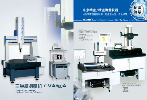
三坐标测量机 CVA800A
·优异的机构,保证了设备的精度 ·强大的CALYPSO软件功能,是操作更方便
……
RONDCOM 54DX 圆度·圆柱度形状测量机
·回转精度高 ·可操作性强 ·测量效率高 ·节省空间设计
……
世界NO.1的回转精度 全CNC大型圆柱度测量机RONDCOM76A,每平 动轴都以严格的直线度精度加工保证。
提高了效率 ·备注功能,方便数据处理
杰出的分析功能:
·测台阶高度 ·多种补偿功能 ·刻槽功能 ·各种曲线
SURFCOM 480A
多种输出方式:
·通过打印单元,
SURFCOM 130A
只需按一个按钮即可实时打印出结果,方便快捷。
·连接电脑,扩大数据功能
130A/480A 技术参数
型号
SURFCOM 130A
RONDCOM 76A 圆度·圆柱度测量机
订货编号:MI-94015-00
特点
·回转精度0.04+3H/10000(JIS B7451),直线度精度1.3μm/700mm(使用700mm测杆),业界第一个X,Y,Z轴,θ采用每轴高精密空气轴承 ·主体结构采用天然花岗岩材料,稳定无时效变形 ·7轴全CNC控制,XY工作台、R轴直线度的精度保证、支持平行性 ·同轴度等测定工作,最大驱动速度100mm/sec、效率,减少测量时间,提供多种自动测量工作
“同君会”的依托: (1)中国多家会员单位的支持; (2)国际众多知名品牌的鼎立相助; (3)大批高科技专业技术人才的加盟; (4)优秀的国际采购团队; (5)高素质的销售及服务团队, (6)多家银行资金售信支持。
同君会全体成员本着精益求精的工作态度,以共同创造价值为理念,不断进取,努力开拓降 低成本,珍惜与您的每次合作机会,我们的发展离不开您的信任与支持,愿继续与您精诚合 作,与各界有识之士携手联盟,为我们的共同事业发展而奋斗!!!
技嘉 M2432 说明书

English11* The illustrations in this document may appear differently from your model.2Congratulations on your purchase of the GIGABYTE Notebook.This Manual will help you to get started with setting up your notebook. For more detailed information, please visit our website at .All specifications are subject to the manufacturer's configuration at the time of shipping and may change without prior notice, written or otherwise.AC Adapter Power Cord Battery Pack Driver CD Manaual Global WarrantyCardHandy BagCheck Supplied ItemsUsing GIGABYTE Notebook for the First Time12To install the battery please follow these steps:Insert the battery pack into the compartment.Remember to slide the switch to the “Lock” position.complete the setup of the Windows Operating System.English3Your GIGABYTE Notebook Tour 3Top ViewLeft View● Smart Setup–Under off condition, Push “Smart+” to enter “smart setup” menu in off mode. You can choose BIOS Setup Utility system recovery in the setup menu.● Smart Manager–In Windows Mode Press “Smart +” button to initiate “Smart Manager”. Bluetooth Status LED Wireless Lan Status LED HDD Status LED Battery Status LED Power Status LED ♦Press the right button of touchpad to check the remaining battery power.E n g l i s h4Base ViewRight ViewEnglish 5HotkeysThe computer employs hotkeys or key combinations to access most of the computer’s controls like screen brightness and volume output. To activate hotkeys, press and hold the <Fn> key before pressing the other key in the hotkey combination.Fn+F1Sleep Puts the computer in Sleep mode.Fn+F2Wireless LAN Enables/disables the Wireless LAN function.Fn+F3Brightness Down Decrease the screen brightness.Fn+F4Brightness Up Increases the screen brightness.Fn+F5Display Toggle Switches display output between the display screen, external monitor (if connected) and both.Fn+F6Touchpad Toggle Turns the internal touchpad on and off.Fn+F7Speaker Toggle Turns the speaker on and off.Fn+F8Volume Down Decreases the sound volume.Fn+F9Volume Up Increases the sound volume.Fn+F10N/A There is no function for this model.Fn+F11Bluetooth Enables/disables the Bluetooth function.Fn+F12Webcam Turns the internal webcam on and off.Fn+EscODD Eject To eject ODD.Fn+~Screen Display Toggle Turns the screen display on and off.Fn +Playback Media Playback control. (Optional)E n g l i s h 6GIGABYTE Software Application 4● GIGABYTE Smart Manager You can activate GIGABYTE Smart Manager by double clicking on the shortcut icon on the desktop if the machine you purchased has the operation system built-in. GIGABYTE Smart Manager is an icon-based control interface, enabling users to intuitionally access common system setup as well as GIGABYTE exclusive utilities. Please be noted that the GIGABYTE Smart Manager interface, icons, utilities and software versions may vary based on the purchased models. Please operate GIGABYTE Smart Manager according to the actual version built-in.●GIGABYTE Smart SwitchGIGABYTE Smart Switch allows users to switch Windows® 7 system toeither 64-bit or 32-bit. The Smart Switch can be accessed from thedesktop (see figure icon).You can also access Smart Switch from Windows Gadget.(see figure icon).The handle position helps to show the current mode, and serves as a tool to switch to another mode by pulling it down. Following dialog box will show up when the icon is clicked to toggle between modes.The system will ask you to save all your work before proceed. System will reboot and change to the mode selected in previous step.programs are saved separately). Therefore, you will need to install the software in both modes if you would like to use it in both modes.English 7●GIGABYTE Smart Recoveryeither 64-bit or 32-bit operating system).1.Two options will appear when entering into Smart Recovery.2.Both 64-bit and 32-bit systems will be restored back to factory defaults whenpressing “Start” button.3.Y ou can choose to restore either the 64-bit or the 32-bit system back to its factory defaults in“Advanced Option” (select from the sub-menu after pressing “Advanced Option”).4.Press “Exit” to quit from Smart Recovery.● GIGABYTE Smart SetupDuring the off mode, press SMART button to enter “Smart Setup” menu. You canchoose BIOS Setup Utility, System Recovery, and other functions in this setup menu.E n g l i s h 8Press”Continue to OS” button to enter operating system.Press”BIOS Setup Utility” button to enter BIOS setup utility.Press”System Recovery” button to enter GIGABYTE Xpress Recovery.Press”Shutdown” button to shutdown the system.* This specification is for users’ reference only. The final configuration depends on the users' bought.■ Warranty & ServiceWarranty and service and related information please refer to the warranty card or GIGABYTE service website as the below link:/support-downloads/technical-support.aspx ■ FAQFAQ (Frequent Asked Questions) please refer to the below link:/support-downloads/faq.aspx Specification & Appendix5。
M2规格书_V4.0

目录修改历史 (1)1. 目录 (2)2. 产品概述 (3)1.产品规格…….……………………………………………………………………………..…3--52.产品外观……………..……………………………………………………………………….5--62.1.正面效果图 (6)2.2.背面效果图 (6)3.主要接口定义………………………………………………………………………………..7-143.1.内置插座接口定义…………………………………………………………....…7--133.2.外置插座接口定义………..……………………………………………………..13--144.板卡尺寸及器件分布图………………………………………………………………..15--164.1.器件正面分布图 (15)4.2.器件背面分布图 (15)4.3.板卡尺寸及镙丝分布图 (16)5. 设备支持列表 (17)n产品概述数字标牌双核主板M2,采用全志A20主控双核芯片,集成两个ARM Mail-400MP图形处理单元,有着很强的视频处理能力,可以兼容大部分的视频格式及解码能力。
背面效果图n主要接口定义▼以下为内置插座接口定义否则容易出现烧掉显示屏电路(关于显示屏电压请查询相应的屏规格书)很重要u CON13 SPK-OUT 接口(2.00MM插座)序号定义属性描述1LOUTP L输出正LOUTP2 LOUTN L输出负LOUTN3 ROUTN R输出负ROUTN4 ROUTP R输出正ROUTN此为双喇叭连接,在使用单喇叭的时候是PIN 1与PIN 2一组,PIN 3与PIN 4一组,不要搞错喇叭的使用请先连接好喇叭后再开机,不要热拔插使用。
u CON10 IR 红外连接接口(2.54MM插针)序号定义属性描述1VCC-3V0输出电源3.0V输出2GND地线地线3 IR 输入IR信号输入(备注:CON10插座可以根据需要焊接一个3PIN插座,以通过延长线外接)u CON20 USB-HOST 接口(2.0MM插座)序号定义属性描述1 VCC-5V 电源输出VCC-5V2 DM 数据负DM3 DP 数据正DP4 GND 地GND(备注:CON20插座只在WIFI模块不使用的情况下,才可作为USB HOST功能来使用。
3.2存储卡
高等教育出版社
TM
17
17
Memory Stick
发展历史
1997年,日本索尼公司独自研制出了记忆棒( Memory Stick),记忆棒几乎可以用在所有索尼 影音产品上。 记忆棒外形轻巧,可为个人电脑、电视、电话、 数码照相机、摄像机和便携式个人视听器材提供 高速、大容量的数字信息储存介质。
高等教育出版社
TM
18
18
Memory Stick
Memory Stick的规格
记忆棒目前主要有三种规格的产品,Memory Stick、Memory Stick PRO Duo 和Memory Stick Micro 。 Memory Stick尺寸为50mm×21.5mm×2.8mm。 PRO Duo尺寸为31mm×20mm×1.6mm。 Micro的尺寸为15mm×12.5mm×1.2mm。
高等教育出版社
TM
15
15
SD卡
SD大容量卡SDHC
SD大容量卡SDHC(SD High-Capacity)的可移 动存储能力比SD标准卡更大,其存储容量范围从 4GB至32GB。 SDHC卡已在数码相机市场占据了相当的市场份 额。
高等教育出版社
TM
16
16
SD卡
应用现状
SD技术目前已成为存储卡的行业标准之一,应用 领域超过400种品牌,涵盖数十种产品类别及超 过8000种机型。 在移动电话、数码音频播放器、汽车导航系统、 电子书籍的数码存储领域中,SD内存卡位居市场 领导地位。 SD内存卡也广泛用于数码相机、手持式PC、游 戏机、打印机、摄像机,以及其它消费型电子产 品。
htf4c32_64_128x64hz(镁光32MegX64 DDR2内存模组用户手册)
DDR2 SDRAM SODIMMMT4HTF3264HZ – 256MB MT4HTF6464HZ – 512MB MT4HTF12864HZ – 1GB Features•200-pin, small-outline dual in-line memory module (SODIMM)•Fast data transfer rates: PC2-3200, PC2-4200,PC2-5300, or PC2-6400•256MB (32 Meg x 64), 512MB (64 Meg x 64), 1GB (128 Meg x 64)•V DD = V DDQ = 1.8V •V DDSPD = 1.7–3.6V•JEDEC-standard 1.8V I/O (SSTL_18-compatible)•Differential data strobe (DQS, DQS#) option •4n -bit prefetch architecture•Multiple internal device banks for concurrent opera-tion•Programmable CAS latency (CL)•Posted CAS additive latency (AL)•WRITE latency = READ latency - 1 t CK •Programmable burst lengths (BL): 4 or 8•Adjustable data-output drive strength •64ms, 8192-cycle refresh •On-die termination (ODT)•Halogen-free•Serial presence detect (SPD) with EEPROM •Gold edge contacts •Single rankFigure 1: 200-Pin SODIMM (MO-224 R/C C)Module height: 30mm (1.181in)OptionsMarking•Operating temperature–Commercial (0°C ≤ T A ≤ +70°C)None –Industrial (–40°C ≤ T A ≤ +85°C)1I •Package–200-pin DIMM (halogen-free)Z •Frequency/CL 2– 2.5ns @ CL = 5 (DDR2-800)-80E – 2.5ns @ CL = 6 (DDR2-800)-800– 3.0ns @ CL = 5 (DDR2-667)-667Notes:1.Contact Micron for industrial temperaturemodule offerings.2.CL = CAS (READ) latency.Table 1: Key Timing ParametersTable 2: AddressingTable 3: Part Numbers and Timing Parameters – 256MB1Table 4: Part Numbers and Timing Parameters – 512MB1Table 5: Part Numbers and Timing Parameters – 1GB Modules1Notes: 1.The data sheet for the base device can be found on Micron’s Web site.2.All part numbers end with a two-place code (not shown) that designates component and PCB revisions.Consult factory for current revision codes. Example: MT4HTF6464HZ-667M1.Pin AssignmentsTable 6: Pin AssignmentsNotes: 1.Pin 85 is NC for 256MB, BA2 for 512MB and 1GB.2.Pin 116 is NC for 256MB and 512MB, A13 for 1GB.Pin DescriptionsThe pin description table below is a comprehensive list of all possible pins for all DDR2modules. All pins listed may not be supported on this module. See Pin Assignments forinformation specific to this module.Table 7: Pin DescriptionsTable 7: Pin Descriptions (Continued)Functional Block DiagramFigure 2: Functional Block DiagramBA[2/1:0]A[13/12:0]RAS#BA[2/1:0]: DDR2 SDRAM A[13/12:0]: DDR2 SDRAM RAS#: DDR2 SDRAM CAS#: DDR2 SDRAM WE#: DDR2 SDRAM CKE0: DDR2 SDRAMODT0: DDR2 SDRAMCK0CK1V REF V SSDDR2 SDRAM DDR2 SDRAMV DD V DDSPDSerial PD DDR2 SDRAM DM3SS256MB, 512MB, 1GB (x64, SR) 200-Pin DDR2 SODIMMFunctional Block DiagramGeneral DescriptionDDR2 SDRAM modules are high-speed, CMOS dynamic random access memory mod-ules that use internally configured 4 or 8-bank DDR2 SDRAM devices. DDR2 SDRAMmodules use DDR architecture to achieve high-speed operation. DDR2 architecture isessentially a 4n-prefetch architecture with an interface designed to transfer two datawords per clock cycle at the I/O pins. A single read or write access for the DDR2 SDRAMmodule effectively consists of a single 4n-bit-wide, one-clock-cycle data transfer at theinternal DRAM core and eight corresponding n-bit-wide, one-half-clock-cycle datatransfers at the I/O pins.DDR2 modules use two sets of differential signals: DQS, DQS# to capture data and CKand CK# to capture commands, addresses, and control signals. Differential clocks anddata strobes ensure exceptional noise immunity for these signals and provide precisecrossing points to capture input signals. A bidirectional data strobe (DQS, DQS#) istransmitted externally, along with data, for use in data capture at the receiver. DQS is astrobe transmitted by the DDR2 SDRAM device during READs and by the memory con-troller during WRITEs. DQS is edge-aligned with data for READs and center-alignedwith data for WRITEs.DDR2 SDRAM modules operate from a differential clock (CK and CK#); the crossing ofCK going HIGH and CK# going LOW will be referred to as the positive edge of CK. Com-mands (address and control signals) are registered at every positive edge of CK. Inputdata is registered on both edges of DQS, and output data is referenced to both edges ofDQS, as well as to both edges of CK.Serial Presence-Detect EEPROM OperationDDR2 SDRAM modules incorporate serial presence-detect. The SPD data is stored in a256-byte EEPROM. The first 128 bytes are programmed by Micron to identify the mod-ule type and various SDRAM organizations and timing parameters. The remaining 128bytes of storage are available for use by the customer. System READ/WRITE operationsbetween the master (system logic) and the slave EEPROM device occur via a standardI2C bus using the DIMM’s SCL (clock) SDA (data), and SA (address) pins. Write protect(WP) is connected to V SS, permanently disabling hardware write protection.Electrical SpecificationsStresses greater than those listed may cause permanent damage to the module. This is astress rating only, and functional operation of the module at these or any other condi-tions outside those indicated in the device data sheet are not implied. Exposure to abso-lute maximum rating conditions for extended periods may adversely affect reliability. Table 8: Absolute Maximum RatingsNotes: 1.The refresh rate is required to double when T C exceeds 85°C.2.For further information, refer to technical note TN-00-08: "Thermal Applications," avail-able on Micron’s Web site.DRAM Operating ConditionsRecommended AC operating conditions are given in the DDR2 component data sheets.Component specifications are available on Micron's Web site. Module speed grades cor-relate with component speed grades.Table 9: Module and Component Speed GradesDesign ConsiderationsSimulationsMicron memory modules are designed to optimize signal integrity through carefully de-signed terminations, controlled board impedances, routing topologies, trace lengthmatching, and decoupling. However, good signal integrity starts at the system level. Mi-cron encourages designers to simulate the signal characteristics of the system's memo-ry bus to ensure adequate signal integrity of the entire memory system.PowerOperating voltages are specified at the DRAM, not at the edge connector of the module.Designers must account for any system voltage drops at anticipated power levels to en-sure the required supply voltage is maintained.I DD SpecificationsTable 10: DDR2 I DD Specifications and Conditions – 256MB (Die Revision G)Values shown for MT47H32M16 DDR2 SDRAM only and are computed from values specified in the 512Mb (32 Meg x 16)Table 11: DDR2 I DD Specifications and Conditions – 256MB (Die Revision H)Values shown for MT47H32M16 DDR2 SDRAM only and are computed from values specified in the 512Mb (32 Meg x 16)Table 12: DDR2 I DD Specifications and Conditions – 512MB (Die Revision E and G)Values shown for MT47H64M16 DDR2 SDRAM only and are computed from values specified in the 1Gb (64 Meg x 16) com-Table 13: DDR2 I DD Specifications and Conditions – 512MB (Die Revision H)Values shown for MT47H64M16 DDR2 SDRAM only and are computed from values specified in the 1Gb (64 Meg x 16) com-Table 14: DDR2 I DD Specifications and Conditions – 512MB (Die Revision M)Values shown for MT47H64M16 DDR2 SDRAM only and are computed from values specified in the 1Gb (64 Meg x 16) com-Table 15: DDR2 I DD Specifications and Conditions – 1GB (Die Revision C)Values shown for MT47H128M16 DDR2 SDRAM only and are computed from values specified in the 2Gb (128 Meg x 16)Serial Presence-DetectFor the latest SPD data, refer to Micron's SPD page: /SPD .Table 16: SPD EEPROM Operating ConditionsTable 17: SPD EEPROM AC Operating ConditionsNotes:1.To avoid spurious start and stop conditions, a minimum delay is placed between SCL = 1and the falling or rising edge of SDA.2.This parameter is sampled.3.For a restart condition or following a WRITE cycle.4.The SPD EEPROM WRITE cycle time (t WRC) is the time from a valid stop condition of awrite sequence to the end of the EEPROM internal ERASE/PROGRAM cycle. During the WRITE cycle, the EEPROM bus interface circuit is disabled, SDA remains HIGH due to pull-up resistance, and the EEPROM does not respond to its slave address.256MB, 512MB, 1GB (x64, SR) 200-Pin DDR2 SODIMMSerial Presence-DetectModule DimensionsFigure 3: 200-Pin DDR2 SODIMMTYPNotes:1.All dimensions are in millimeters (inches); MAX/MIN or typical (TYP) where noted.2.The dimensional diagram is for reference only. Refer to the JEDEC MO document for ad-ditional design dimensions.8000 S. Federal Way, P .O. Box 6, Boise, ID 83707-0006, Tel: /productsupport Customer Comment Line: 800-932-4992Micron and the Micron logo are trademarks of Micron Technology, Inc.All other trademarks are the property of their respective owners.This data sheet contains minimum and maximum limits specified over the power supply and temperature range set forth herein.Although considered final, these specifications are subject to change, as further product development and data characterization some-times occur.256MB, 512MB, 1GB (x64, SR) 200-Pin DDR2 SODIMMModule Dimensions。
VGA、QVGA、WVGA、HVGA

VGA、QVGA、WVGA、HVGA名词解释及区别WQVGAWQVGA全称:Wide Quarter Video Graphics Array数码产品屏幕分辨率的一种,代表480X272(宽高比16:9)或者400X240(宽高比5:3)的屏幕分辨率,而不是国内厂商标称的480X240比QVGA(320×240)分辨率高比VGA(640×480)分辨率低续VGA后,逐渐诞生出QVGA、WVGA、HVGA分辨率产品,这分辨率都手机参数里随处可见,下面是VGA、QVGA、WVGA、HVGA分名词解释及区别。
VGA即“Video Graphics Array”。
是IBM在1987年随PS/2机一起推出的一种视频传输标准,具有分辨率高、显示速率快、颜色丰富等优点,在彩色显示器领域得到了广泛的应用。
VGA最早指的是显示器640X480。
VGA的英文全称是Video Graphic Array,也叫显示绘图阵列。
多普达手机中S900C+就是典型的QVGA即"Quarter VGA"。
中VGA的四分之一尺寸,亦即在液晶屏幕(LCD)上输出的分辨率是240×320像素。
QVGA支持屏幕旋转,可以开发出相应的程序,以显示旋转90°、180°、270°屏幕位置。
由Hand Era公司发布。
多用于手持/移动设备。
WVGA即“Wide VGA” 。
其分辩率为800×480象素。
是扩大了VGA(640×480)的分辨率。
应用于PDA和手机等,因为很多网页的宽度都是800,所以WVGA的屏幕会更加适和于浏览网页,可以说是未来手持设备的分辨率的大趋势。
HVGA即“Half-size VGA”。
是VGA的一半,分辨率为(480*320),(3:2宽高比),它是用于各种各样的PDA设备,首先是2002年的索尼Clie PEG - NR70,黑莓手机也有HVGA的,iPhone也是HVGA设备。
解析HDMI线材规格与技术标识

解析HDMI线材规格与技术标识通道线材采样频率hdmi线图像分辨率一直以来人们对于HDMI的认识只停留在其版本上,其实HDMI Ver.1.0发布时,HDMI就已经支持1080/60p、192kHz/24bit以及7.1声道的传送了,一直到2006年HDMI的版本已经发展到了1.3a,支持2560×1600分辨率的图像传送,并且加入了对16bit Deep Color以及高清音频格式的支持。
HDMI在目前的影音器材中应用得十分广泛,除了一般的高清显示设备外,高清播放设备、高清摄录设备以及AV放大器都加入了HDMI连接端子,甚至连DVD机和SACD机都使用上了HDMI接口,HDMI的普及率已经非常高。
去年6月,HDMI又公布了全新的HDMI Ver.1.4版本,并且增加了对于3D图像传送的支持,而在今年的3月4日,我们又看到了全新的HDMI Ver.1.4a的面世,那么这个1.4与1.4a之间到底有哪些进化和那些新功能的加入呢?带着这些问题,我们请教了Golden Sound中国区总经理余瑞忠先生,余先生对于HDMI的产品有着十分丰富的知识,下面就是余先生为大家所做的详细讲解。
HDMI Ver.1.4规格包含许多内容要了解1.4与1.4a之间的差别,首先就要了解一下HDMI Ver.1.4版本所包含的内容。
1.4版本的HDMI线材以及器材必须支持1080p、1080i、720p、480p、480i、576p、576i的图像分辨率传送,在图像扫描频率上可以支持从23.98Hz到240Hz的覆盖,另外还有我们经常所说的4K2K分辨率。
以往HDMI线所支持的图像分辨率:1280x720 24Hz/25Hz/30Hz/50Hz/60Hz1920x1080 24Hz/25Hz/30Hz/50Hz/60HzHDMI Ver.1.4新提出的可支持图像分辨率:3840x2160 24Hz/25Hz/30Hz4096x2160 24Hz细心的朋友可以发现3840x2160与4096x2160分辨率的图像,通过HDMI Ver.1.4传送只可支持24Hz的刷新频率,而按照线材的带宽和信号的数据量进行对比,3840x2160 24Hz/25Hz/30Hz 和4096x2160 24Hz 在资料传送过程中需要的带宽都在10.2Gbps以内,因此我们可以发现,1.3与1.4版本的HDMI线材的频宽其实是相同的,而采样频率同为最高的340MHz。
方正文峰 ML 320 320D 系列复印机 网络指南
• RSA Data Security, Inc. MD5 Message-Digest Algorithm © 1991-2, RSA Data Security, Inc. 1991。版权所有。 仅当在提及或参考本软件或本功能的任何资料中都注明 “RSA Data Security, Inc. MD5 MessageDigest Algorithm”时,才授权复制和使用本软件。 仅当在提及或参考本软件衍生产品的任何资料中都注明 “RSA Data Security, Inc. MD5 MessageDigest Algorithm”时,才授权开发和使用本软件的衍生产品。 RSA Data Security, Inc. 对于本软件的商业性或相对特定目的的适用性,未作任何明确表述。本软件 “按实物原样”供货,不带任何明确或隐含的保证。 在本资料或软件的任何副本中,都必须保留这些声明。
2. 将网络电缆连接到网络
确认连接 ...................................................................................................... 9 连接到 Ethernet 接口 ............................................................................................ 10
功能或者相关功能, ML 320/320D 系列复印机不支持。 方正文峰 ML 320/320D 系列复印机不提供 IEEE 1394 接口板、IEE E 802.11b 无线 LAN 板、Bluetooth 单元、PostScript3 单元等选件。 方正文峰 ML 320/320D 系列复印机不支持 Macintosh 打印。
高保真 4x2 HDMI 矩阵
使用手册高保真4x2 HDMI 矩阵产品型号:HDMX0402M2享受高清影像世界备注本公司保留不需要通知本手册读者而对产品实物的包装及其相关文档进行修改的权利。
4x2HIFI HDMI Matrix是本公司的注册商标。
© 2009本公司版权所有引言尊敬的客户:您好!非常感谢您购买本公司的产品。
为了实现产品的最佳效果和保证安全,请您在对产品进行连接、操作、调试前仔细阅读本手册。
此手册请予以保留,以备将来查阅。
本公司所生产的HDMI切换器、网线延长器、矩阵、分配器等系列产品,其设计之目的是为了让您的影音设备使用起来更便捷,更舒适,更高效,更节能。
这款高保真的4x2 HDMI 矩阵可以把四个高清信号源与两个高清信号端同时连接起来,同时输出端音频可以光纤或者立体声耳机输出。
它可以很容易地将四路高清信号在两个兼容高清信号的显示器或者投影机上自由切换或者分配,而且任意一个输出端口都可以通过光纤或者立体声耳机实现音频的独立输出。
并支持ARC功能, 在高清电视直接接收音频和视频内容的情况下,将高清电视通过HDMI线把音频直接传送到A/V功放接收机上。
本公司所生产设备为以下应用提供解决方案:如对噪声、传输距离及安全有限制的场所、数据中心控制、信息分配、会议室演示以及教学环境和公司培训场所。
本公司真诚希望能够以最优惠的价格提供给客户最好的产品。
产品所售价格包含了来自公司卓越工程师团队的终身技术支持服务。
产品特点:●一路MHL/HDMI双模输入,三路HDMI信号输入切换或分配到二个HDMI 显示设备上●任意一个信号端都可以通过光纤或者立体声耳机实现音频独立输出●可实现音频同步分离输出,有2CH、5.1CH、ADV三种音频模式可选择●支持全高清、全3D●支持4K*2K分辨率●支持24位/ 30位/36位/48位深色●支持蓝光DVD24/50/60fs/HD-DVD/xvYCC●音频格式DTS-HD/Dolby-trueHD/LPCM7.1/DTS/DOLBY-AC3/DSD/HD(HBR)●支持信号时序重整●使用AWG24 HDMI标准线缆,输入传输距离可达15米,输出传输距离可达25米。
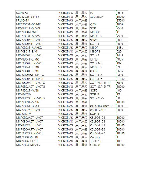
MEMORY存储芯片MT48LC4M32B2TG-6IT G中文规格书
5.CA parity = Disable, CS to CA latency = Disable, Write DBI = Disable, Write CRC = Disable.6.t CCD_S/L = 5 isn’t allowed in 2t CK preamble mode.7.The write recovery time (t WR) and write timing parameter (t WTR) are referenced fromthe first rising clock edge after the last write data shown at T20.8.When operating in 2t CK WRITE preamble mode, CWL may need to be programmed to avalue at least 1 clock greater than the lowest CWL setting supported in the applicablet CK range, which means CWL = 9 is not allowed when operating in 2t CK WRITE pream-ble mode.Figure 178: WRITE (BC4) OTF to WRITE (BC4) OTF with 1t CK Preamble in Different Bank GroupCommand DQ CK_t CK_cDQS_t,DQS_cBank GroupAddress Address Notes: 1.BC4, AL = 0, CWL = 9, Preamble = 1t CK.2.DI n (or b ) = data-in from column n (or column b ).3.DES commands are shown for ease of illustration; other commands may be valid atthese times.4.BC4 setting activated by MR0[1:0] = 01 and A12 = 0 during WRITE commands at T0 andT4.5.CA parity = Disable, CS to CA latency = Disable, Write DBI = Disable, Write CRC = Disable.6.The write recovery time (t WR) and write timing parameter (t WTR) are referenced fromthe first rising clock edge after the last write data shown at T17.4Gb: x4, x8, x16 DDR4 SDRAM WRITE OperationTable 91: DQ Input Receiver Specifications (Continued)Notes: 1.All Rx mask specifications must be satisfied for each UI. For example, if the minimum in-put pulse width is violated when satisfying TdiVW (MIN), V diVW,max , and minimum slew rate limits, then either TdiVW (MIN) or minimum slew rates would have to be increased to the point where the minimum input pulse width would no longer be violated.2.Data Rx mask voltage and timing total input valid window where V diVW is centered around V CENTDQ,midpoint after V REFDQ training is completed. The data Rx mask is applied per bit and should include voltage and temperature drift terms. The input buffer design specification is to achieve at least a BER =1e- 16 when the Rx mask is not violated.3.Defined over the DQ internal V REF range 1.4.Overshoot and undershoot specifications apply.5.DQ input pulse signal swing into the receiver must meet or exceed V IHL(AC)min . V IHL(AC)min is to be achieved on an UI basis when a rising and falling edge occur in the same UI (a valid TdiPW).6.DQ minimum input pulse width defined at the V CENTDQ,midpoint .7.DQS-to-DQ Rx mask offset is skew between DQS and DQ within a nibble (x4) or word (x8, x16 [for x16, the upper and lower bytes are treated as separate x8s]) at the SDRAM balls over process, voltage, and temperature.8.DQ-to-DQ Rx mask offset is skew between DQs within a nibble (x4) or word (x8, x16) at the SDRAM balls for a given component over process, voltage, and temperature.9.Input slew rate over V diVW mask centered at V CENTDQ,midpoint . Slowest DQ slew rate to fastest DQ slew rate per transition edge must be within 1.7V/ns of each other.10.Input slew rate between V diVW mask edge and V IHL(AC)min points.The following figure shows the Rx mask relationship to the input timing specifications relative to system t DS and t DH. The classical definition for t DS/t DH required a DQ rising 4Gb: x4, x8, x16 DDR4 SDRAM Electrical Characteristics – AC and DC Single-Ended Input Measurement Levels。
HMD系列RAM中文数据手册

HMD系列RAM中文数据手册一、引言HMD系列RAM(Random Access Memory,随机存取存储器)是一种用于计算机和其他电子设备中的主存储器。
本手册旨在提供关于HMD系列RAM的详细技术规格和特性的中文数据。
二、产品概述HMD系列RAM是一种高性能、高稳定性的存储器解决方案,适用于各种计算机和电子设备的存储需求。
该系列RAM采用先进的半导体技术,具有快速读写速度、低功耗和可靠性高的特点。
三、主要特性1. 存储容量:HMD系列RAM提供多种存储容量选项,包括1GB、2GB、4GB、8GB和16GB等。
用户可根据实际需求选择合适的存储容量。
2. 数据传输速度:HMD系列RAM具有高速的数据传输速度,可提供每秒5000MB的读取速度和4000MB的写入速度,有效提高计算机和设备的运行效率。
3. 电源电压:HMD系列RAM采用标准的电源电压,为1.2V,可在低功耗的情况下提供稳定的性能。
4. 接口类型:HMD系列RAM支持多种接口类型,包括DDR3、DDR4和LPDDR4等,以满足不同设备的需求。
5. 工作温度范围:HMD系列RAM可在广泛的工作温度范围内正常运行,包括-40℃至85℃,适用于各种环境条件下的应用。
四、性能参数1. 时序参数:- tRAS(行地址选通到有效数据出现):15ns - tRCD(行地址选通到列地址选通):10ns - tRP(行地址选通到行预充电):10ns- tRC(行地址选通到行循环时间):45ns- tRRD(行地址选通到行地址选通):5ns- tWR(写入时序):15ns- tRTP(行地址选通到读命令周期):7.5ns - tWTR(写命令到读命令周期):7.5ns2. 电气参数:- 电源电压:1.2V- 电流消耗:100mA- 工作频率:2400MHz- 数据总线宽度:64位- 内存芯片数量:16颗- 纠错编码:ECC(Error Correction Code)3. 可靠性参数:- 工作寿命:100,000小时- 数据保持时间:10年- 错误率:小于10^-15五、应用领域HMD系列RAM广泛应用于以下领域:1. 个人电脑和笔记本电脑2. 服务器和数据中心3. 移动设备,如智能手机和平板电脑4. 嵌入式系统和工控设备5. 汽车电子和航空航天等领域六、安装和使用指南1. 安装要求:在安装HMD系列RAM之前,请确保计算机或设备已经关闭,并且断开了电源连接。
MEMORY存储芯片MT46V32M4TG-75L中文规格书
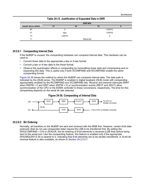
DX DRT o CPU or EDMA controller ArchitectureTable 24-12.Justification of Expanded Data in DRRRJUST Bit in SPCRDRR Bits3116150000LAW1601sign LAW1610LAW16011Reserved 24.2.8.1Companding Internal DataIf the McBSP is unused,the companding hardware can compand internal data.This hardware can be used to:•Convert linear data to the appropriate μ-law or A-law format.•Convert μ-law or A-law data to the linear format.•Observe the quantization effects in companding by transmitting linear data and compressing and re-expanding this data.This is useful only if both XCOMPAND and RCOMPAND enable the samecompanding format.Figure 24-36shows the method by which the McBSP can compand internal data.The data path is indicated by the (DLB)arrow.The McBSP is enabled in digital loopback (DLB)mode with companding appropriately enabled by the RCOMPAND and XCOMPAND bits.Receive and transmit interrupts (RINT when RINTM =0and XINT when XINTM =0)or synchronization events (REVT and XEVT)allowsynchronization of the CPU or the EDMA controller to these conversions,respectively.The time for this companding depends on the serial bit rate selected.Figure panding of Internal Data24.2.8.2Bit OrderingNormally,all transfers on the McBSP are sent and received with the MSB first.However,certain 8-bit data protocols (that do not use companded data)require the LSB to be transferred first.By setting the(R/X)COMPAND =01b in (R/X)CR,the bit ordering of 8-bit elements is reversed (LSB first)before being sent to the serial port.Like the companding feature,this feature is enabled only if the appropriate(R/X)WDLEN1/2bit is cleared to 0,indicating that 8-bit elements are to be serially transferred.A 32-bit bit reversal feature is also available,as shown in Section 24.2.5.5.7DXArchitectureFigure24-30.Decision Tree Response to Transmit Frame Synchronization Pulse Figure24-31.Unexpected Transmit Frame Synchronization Pulse。
- 1、下载文档前请自行甄别文档内容的完整性,平台不提供额外的编辑、内容补充、找答案等附加服务。
- 2、"仅部分预览"的文档,不可在线预览部分如存在完整性等问题,可反馈申请退款(可完整预览的文档不适用该条件!)。
- 3、如文档侵犯您的权益,请联系客服反馈,我们会尽快为您处理(人工客服工作时间:9:00-18:30)。
HANBit HMD4M32M2VEGENERAL DESCRIPTIONThe HMD4M32M2VE is a 4M x 32 bit dynamic RAM high-density memory module. The module consists of two CMOS 4M x 16 bit DRAMs in 50-pin TSOP packages mounted on a 72-pin. A 0.1 or 0.22uF decoupling capacitor is mounted on the printed circuit board for each DRAM components. The module is a single In-line memory module with edge connections and is intended for mounting in to 72-pin edge connector sockets. All module components may be powered from a single 3.3V DC power supply. All inputs and outputs are LVTTL-compatible.FEATURESw Part IdentificationHMD4M32M2VE----Lead finish Solder HMD4M32M2VEG- Lead finish Gold w Access times : 50, 60ns w High-density 16MByte design w 4K Cycles/64ms Ref, Gold w Single +3.3V ± 0.3V power supply w JEDEC standard pinout w EDO Mode operationw LVTTL compatible inputs and outputs w FR4-PCB designOPTIONS MARKINGw Timing50ns access -5 60ns access -6 w Packages72-pin SIMM MPERFORMANCE RANGESpeed tRAC tCAC tRC 5 50ns 13ns 84ns 660ns15ns104nsPIN NAMESPin Name FunctionPin Name FunctionPin Name Function A0-A11 Address Input(4K Ref) /RAS0 Row Address Strobe Vss Ground DQ0-DQ31 Data In/Out /CAS0 - /CAS3 Column Address Strobe NC No Connection /W Read/Write InputPD1 - PD4Presence DetectVccPower(+3.3V)PIN ASSIGNMENTPINSYMBOLPINSYMBOLPINSYMBOLPINSYMBOL1 VSS 19 A10 37 NC 55 DQ112 DQ0 20 DQ4 38 NC 56 DQ273 DQ16 21 DQ20 39 VSS 57 DQ124 DQ1 22 DQ5 40 /CAS0 58 DQ28 5 DQ17 23 DQ21 41 /CAS2 59 VCC6 DQ2 24 DQ6 42 /CAS3 60 DQ297 DQ18 25 DQ22 43 /CAS1 61 DQ13 8 DQ3 26 DQ7 44 /RAS0 62 DQ309 DQ19 27 DQ23 45 NC 63 DQ14 10 VCC 28 A7 46 NC 64 DQ31 11 NC 29 A11 47 /W 65 DQ15 12 A0 30 VCC 48 NC 66 NC 13 A1 31 A8 49 DQ8 67 PD1 14 A2 32 A9 50 DQ24 68 PD2 15 A3 33 NC 51 DQ9 69 PD3 16A4 34 NC 52 DQ25 70 PD4 17 A5 35 NC 53 DQ10 71 NC 18A636NC54DQ2672VSSHANBit HMD4M32M2VEFUNCTIONAL BLOCK DIAGRAMToall DRAMs0.1uF or 0.22uFCapacitorfor each DRAMDQ0-DQ7DQ8-DQ15DQ16-DQ23DQ24-DQ31/RAS0/CAS0/CAS1/CAS2/CAS3/WA0-A11Vcc VssHANBit HMD4M32M2VE ABSOLUTE MAXIMUM RATINGSPARAMETER SYMBOL RATINGVoltage on Any Pin Relative to Vss V IN ,OUT-0.5V to 6.5VVoltage on Vcc Supply Relative to Vss Vcc -0.5V to 4.6VPower Dissipation P D2WStorage Temperature T STG-55o C to 150o CShort Circuit Output Current I OS50mAw Permanent device damage may occur if " Absolute Maximum Ratings" are exceeded. Functional operation should be restricted to the conditions as detailed in the operational sections of this data sheet. Exposure to absolute maximum rating conditions for extended periods may affect device reliability.RECOMMENDED DC OPERATING CONDITIONS( Voltage reference to V SS, T A=0 to 70 o C )PARAMETER SYMBOL MIN TYP. MAX UNIT Supply Voltage Vcc 3.0 3.3 3.6 V Ground Vss 0 0 0 V Input High Voltage V IH 2.0 - +5.5 V Input Low Voltage V IL-0.3 - 0.8 VDC AND OPERATING CHARACTERISTICSSYMBOL SPEED MIN MAX UNITS-5 - 220 mAI CC1-6 - 200 mAI CC2- 4 mA-5 - 220 mAI CC3-6 - 200 mA-5 - 220 mAI CC4-6 - 200 mAI CC5- 600 mA-5 - 220 mAI CC6-6 - 200 mAI l(L)-10 10 µAI O(L)-10 10 µAV OH 2.4 - VV OL- 0.4 VI CC1 : Operating Current * (/RAS , /CAS , Address cycling @t RC=min.)I CC2 : Standby Current ( /RAS=/CAS=V IH )HANBit HMD4M32M2VEI CC3 : /RAS Only Refresh Current * (/CAS=V IH, /RAS, Address cycling @t RC=min )I CC4 : Fast Page Mode Current * (/RAS=V IL, /CAS, Address cycling @t PC=min )I CC5 : Standby Current (/RAS=/CAS=Vcc-0.2V )I CC6 : /CAS-Before-/RAS Refresh Current * (/RAS and /CAS cycling @t RC=min )* NOTE: I CC1, I CC3, I CC4 and I CC6 are dependent on output loading and cycle rates. Specified values are obtained with the output open. I CC is specified as an average current. In I CC1 and I CC3, address cad be changed maximum once while /RAS=V IL. In I CC4, address can be changed maximum once within one page mode cycle.CAPACITANCE( TA =25oC, Vcc = 3.3V, f = 1Mz )DESCRIPTION SYMBOL MIN MAX UNITS Input Capacitance (A0-A11) C IN1- 10 pF Input Capacitance (/W) C IN2- 14 pF Input Capacitance (/RAS0, /RAS1) C IN3- 14 pF Input Capacitance (/CAS0-/CAS3) C IN4- 14 pF Input/Output Capacitance (DQ0-31) C DQ1- 14 pFAC CHARACTERISTICS( 0 o C ≤ TA≤ 70o C , Vcc = 3.3V±10%, See notes 1,2.)-5 -6STANDARD OPERATION SYMBOLMIN MAX MIN MAXUNIT Random read or write cycle time t RC84 104 ns Access time from /RAS t RAC50 60 ns Access time from /CAS t CAC13 15 ns Access time from column address t AA25 30 ns /CAS to output in Low-Z t CLZ 3 3 ns Transition time (rise and fall) t T 1 50 1 50 ns /RAS precharge time t RP30 40 ns /RAS pulse width t RAS50 10K 60 10K ns /RAS hold time t RSH13 15 ns /CAS hold time t CSH38 45 ns /CAS pulse width t CAS8 10K 10 10K ns /RAS to /CAS delay time t RCD20 37 20 45 ns /RAS to column address delay time t RAD15 25 15 30 ns /CAS to /RAS precharge time t CRP 5 5 ns Row address set-up time t ASR0 0 ns Row address hold time t RAH10 10 ns Column address set-up time t ASC0 0 nsHANBit HMD4M32M2VEColumn address hold time t CAH8 10 ns Column Address to /RAS lead time t RAL25 30 ns Read command set-up time t RCS0 0 ns Read command hold referenced to /CAS t RCH0 0 ns Read command hold referenced to /RAS t RRH0 0 ns Write command hold time t WCH10 10 ns Write command pulse width t WP10 10 ns Write command to /RAS lead time t RWL10 10 ns Write command to /CAS lead time t CWL8 10 ns Data-in set-up time t DS0 0 ns Data-in hold time t DH8 10 ns Refresh period t REF64 64 ns Write command set-up time t WCS0 0 ns /CAS setup time (C-B-R refresh) t CSR 5 5 ns /CAS hold time (C-B-R refresh) t CHR10 10 ns /RAS precharge to /CAS hold time t RPC 5 5 ns Access time from /CAS precharge t CPA35 40 ns Fast page mode cycle time t PC28 35 ns /CAS precharge time (Fast page) t CP8 10 ns /RAS pulse width (Fast page ) t RASP50 100K 60 100K ns /W to /RAS precharge time (C-B-R refresh) t WRP10 10 ns /W to /RAS hold time (C-B-R refresh) t WRH10 10 ns NOTES1.An initial pause of 200µs is required after power-up followed by any 8 /RAS-only or /CAS-before-/RAS refresh cycles before proper device operation is achieved.2.V IH (min) and V IL (max) are reference levels for measuring timing of input signals. Transition times are measured between V IH(min) and V IL(max) and are assumed to be 5ns for all inputs.3.Measured with a load equivalent to 1TTL loads and 100pF4.Operation within the t RCD(max) limit insures that t RAC(max) can be met. t RCD(max) is specified as a reference point only. If t RCD is greater than the specified t RCD(max) limit, then access time is controlled exclusively by t CAC.5.Assumes that t RCD≥ t RCD(max)6. t AR, t WCR, t DHR are referenced to t RAD(max)7.This parameter defines the time at which the output achieves the open circuit condition and is not referenced to V OHor V OL.8. t WCS, t RWD, t CWD and t AWD are non restrictive operating parameter.They are included in the data sheet as electrical characteristic only. If t WCS≥tWCS(min) the cycle is an early writecycle and the data out pin will remain high impedance for the duration of the cycle.9. Either t RCH or t RRH must be satisfied for a read cycle.10. These parameters are referenced to the /CAS leading edge in early write cycles and to the /W leading edge in read-write cycles.11. Operation within the t RAD(max) limit insures that t RAC(max) can be met. t RAD(max) is specified as a referencepoint only. If t RAD is greater than the specified t RAD(max) limit. then access time is controlled by t AA.HANBit HMD4M32M2VE TIMING DIAGRAMPlease refer to attached timing diagram chart (I)PACKAGING INFORMATIONSIMM DesignORDERING INFORMATIONPart Number Density Org. Package RefreshCycleVcc SPEEDHMD4M32M2VEG-5 16MByte 4MX 32bit 72 Pin-SIMM 4,096 Cycles64ms Ref.3.3V 50nsHMD4M32M2VEG-6 16MByte 4MX 32bit72 Pin-SIMM 4,096 Cycles64ms Ref.3.3V 60ns19.000.25 mm MAX。
