SBT2222AF中文资料
SST2222A中文资料
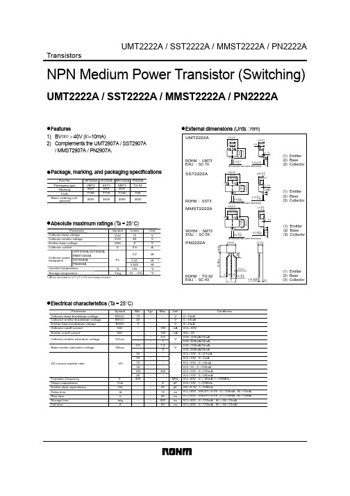
UMT2222A,SST2222A,
MMST2222A
Collector power
dissipation
SST2222A
PC
PN2222A
Junction temperature
Tj
Storage temperature
Tstg
∗ When mounted on a 7 x 5 x 0.6 mm ceramic board
1000 100
Ta=125°C 25°C
−55°C
VCE=10V
10 0.1
1.0
10
100
COLLECTOR CURRENT : Ic(mA)
1000
Fig.4 DC current gain vs. collector current(ΙΙ)
AC CURRENT GAIN : hFE
1000 100
2.3
(1) Emitter (2) Base (3) Collector
!Electrical characteristics (Ta = 25°C)
Parameter Collector-base breakdown voltage Collector-emitter breakdown voltage Emitter-base breakdown voltage Collector cutoff current Emitter cutoff current Collector-emitter saturation voltage
MMST2222A
2.0±0.2 1.3±0.1 0.65 0.65 (1) (2)
0.9±0.1 0.2 0.7±0.1
1.25±0.1 2.1±0.1 0.1 ∼ 0.4
FMB2222A;中文规格书,Datasheet资料
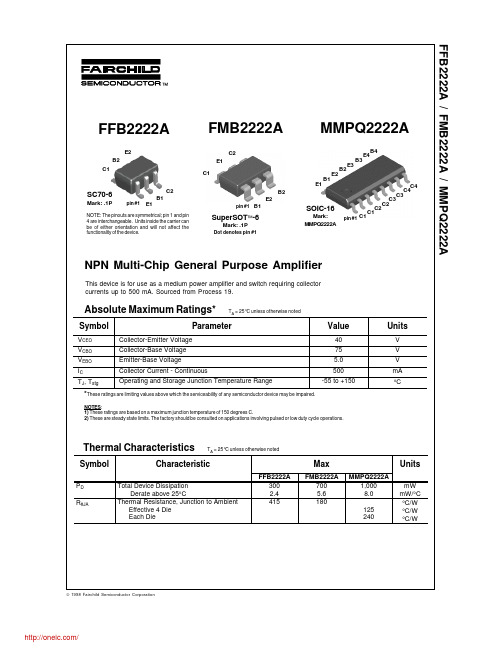
Thermal Characteristics
Symbol
PD RθJA
TA = 25°C unless otherwise noted
Characteristic
Total Device Dissipation Derate above 25°C Thermal Resistance, Junction to Ambient Effective 4 Die Each Die FFB2222A 300 2.4 415
*Pulse Test: Pulse Width ≤ 300 µs, Duty Cycle ≤ 2.0%
Spice Model
NPN (Is=14.34f Xti=3 Eg=1.11 Vaf=74.03 Bf=255.9 Ne=1.307 Ise=14.34f Ikf=.2847 Xtb=1.5 Br=6.092 Nc=2 Isc=0 Ikr=0 Rc=1 Cjc=7.306p Mjc=.3416 Vjc=.75 Fc=.5 Cje=22.01p Mje=.377 Vje=.75 Tr=46.91n Tf=411.1p Itf=.6 Vtf=1.7 Xtf=3 Rb=10)
300
VCE(sat) VBE(sat)
Collector-Emitter Saturation Voltage* Base-Emitter Saturation Voltage*
0.3 1.0 1.2 2.0
V V V V
SMALL SIGNAL CHARACTERISTICS
fT Cobo Cibo NF Current Gain - Bandwidth Product Output Capacitance Input Capacitance Noise Figure IC = 20 mA, VCE = 20 V, f = 100 MHz VCB = 10 V, IE = 0, f = 100 kHz VEB = 0.5 V, IC = 0, f = 100 kHz IC = 100 µA, VCE = 10 V, RS = 1.0 kΩ, f = 1.0 kHz 300 4.0 20 2.0 MHz pF pF dB
PN2222A;中文规格书,Datasheet资料
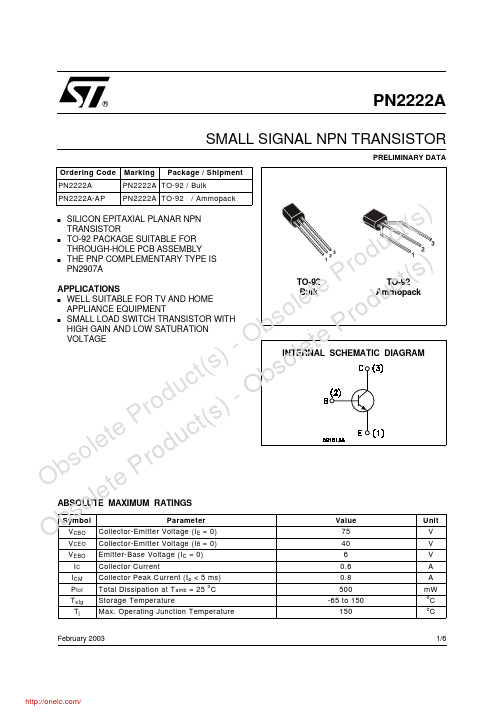
PN2222ASMALL SIGNAL NPN TRANSISTORPRELIMINARY DATAs SILICON EPITAXIAL PLANAR NPNTRANSISTORs TO-92 PACKAGE SUITABLE FOR THROUGH-HOLE PCB ASSEMBLY sTHE PNP COMPLEMENTARY TYPE IS PN2907AAPPLICATIONS s WELL SUITABLE FOR TV AND HOME APPLIANCE EQUIPMENTs SMALL LOAD SWITCH TRANSISTOR WITH HIGH GAIN AND LOW SATURATION VOLTAGEFebruary 2003ABSOLUTE MAXIMUM RATINGS®1/6l e t e P r o d u c t (s ) - O b s o l e t e P r o d u c t (s ) -PN2222ATHERMAL DATAELECTRICAL CHARACTERISTICS (T case = 25 o C unless otherwise specified)Ob s o l e t e P r o d uc t (s ) - O b s o l e t e P r od u c t (s ) ELECTRICAL CHARACTERISTICS(Continued)PN2222AO b s o l e t e P r o d u c t (s ) - O b s o l e t e P r o d u c t (s )PN2222APN2222AOb s o l e t e P r o d uc t (s ) - O b s o l e t e P r od u c t (s ) Information furnished is believed to be accurate and reliable. However, STMicroelectronics assumes no responsibility for the consequences of use of such information nor for any infringement of patents or other rights of third parties which may result from its use. No license is granted by implication or otherwise under any patent or patent rights of STMicroelectronics. Specification mentioned in this publication are subject to change without notice. This publication supersedes and replaces all information previously supplied. STMicroelectronics products are not authorized for use as critical components in life support devices or systems without express written approval of STMicroelectronics.The ST logo is a trademark of STMicroelectronics© 2003 STMicroelectronics – Printed in Italy – All Rights ReservedSTMicroelectronics GROUP OF COMPANIESAustralia - Brazil - Canada - China - Finland - France - Germany - Hong Kong - India - Israel - Italy - Japan - Malaysia - Malta - Morocco - Singapore - Spain - Sweden - Switzerland - United Kingdom - United States.PN2222AO b s o l e t e P r o d u c t (s ) - O b s o l e t e P r o d u c t (s )分销商库存信息: STMPN2222A。
2N2222中文资料_数据手册_参数

Product specification
2N2222; 2N2222A
SYMBOL
PARAMETER
CONDITIONS
MIN. MAX. UNIT
Switching times (between 10% and 90% levels); see Fig.2
DISCRETE SEMICONDUCTORS
DATA SHEET
M3D125
2N2222; 2N2222A NPN switching transistors
Product specification Supersedes data of September 1994 File under Discrete Semiconductors, SC04
DC current gain 2N2222A
IE = 0; VCB = 60 V IE = 0; VCB = 60 V; Tamb = 150 °C IC = 0; VEB = 3 V IC = 0.1 mA; VCE = 10 V IC = 1 mA; VCE = 10 V IC = 10 mA; VCE = 10 V IC = 150 mA; VCE = 1 V; note 1 IC = 150 mA; VCE = 10 V; note 1 IC = 10 mA; VCE = 10 V; Tamb = −55 °C
SYMBOL
PARAMETER
Rth j-a Rth j-c
thermal resistance from junction to ambient thermal resistance from junction to case
CONDITIONS in free air
PT2221_PT2222遥控器芯片资料
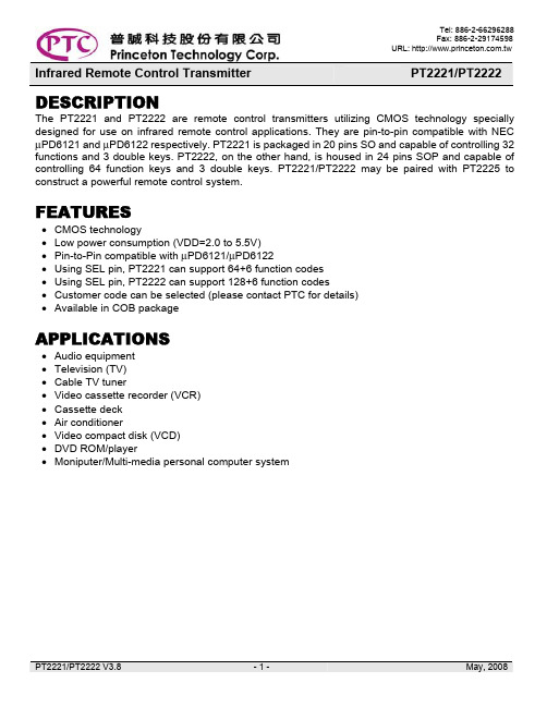
ห้องสมุดไป่ตู้KI7
Key Input/Output Scan Circuit
SE L REM LMP
CCS
KI/O 0 KI/O1 KI/O2 KI/O3 KI/O4 KI/O5 KI/O6 KI/O7
PT2221/PT2222 V3.8
-2-
May, 2008
Infrared Remote Control Transmitter
FEATURES
• CMOS technology • Low power consumption (VDD=2.0 to 5.5V) • Pin-to-Pin compatible with µPD6121/µPD6122 • Using SEL pin, PT2221 can support 64+6 function codes • Using SEL pin, PT2222 can support 128+6 function codes • Customer code can be selected (please contact PTC for details) • Available in COB package
PT2221/PT2222
FUNCTION DESCRIPTION
TRANSMISSION CODE
The transmission code consists of a leader code, 16-bits custom codes, and 8- bits data codes. The inverse code of the data code is also sent simultaneously. The following diagram shows this one frame construction.
MMBT2222_数据手册

MMBT2222 MMBT2222A
VCE(sat)
(I C = 500mAdc, I B = 50 mAdc)
MMBT2222 MMBT2222A
Base–Emitter Saturation Voltage (I C = 150 mAdc, I B = 15 mAdc)
MMBT2222 MMBT2222A
3
1 2
CASE 318–08, STYLE 6 SOT–23 (TO–236AB)
Max
—
Vdc
––
10
nAdc
µAdc 0.01 0.01 10 10
100
nAdc
20
nAdc
O4–1/5
LESHAN RADIO COMPANY, LTD.
MMBT2222LT1 MMBT2222ALT1
rb, C C NF
SWITCHING CHARACTERISTICS
Delay Time
(V CC = 30 Vdc, V EB(off) = – 0.5 Vdc
td
Rise Time
I C = 150 mAdc, I B1 = 15 mAdc)
tr
Storage Time
(V CC = 30 Vdc, I C = 150 mAdc
0.1
0.2 0.3
0.5
1.0
2.0 3.0
5.0
10
20 30 50
I B , BASE CURRENT (mA) Figure 4. Collector Saturation Region
V CE, COLLECTOR–EMITTER VOLTAGE (VOLTS)
O4–3/5
2SK2232中文资料
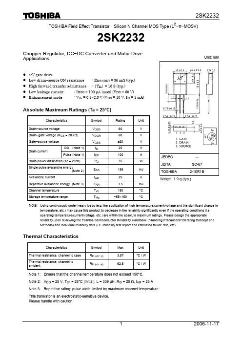
TOSHIBA Field Effect Transistor Silicon N Channel MOS Type (L 2−π−MOSV)2SK2232Chopper Regulator, DC −DC Converter and Motor Drive Applicationsz 4-V gate drivez Low drain −source ON resistance : R DS (ON) = 36 m Ω (typ.) z High forward transfer admittance : |Y fs | = 16 S (typ.)z Low leakage current : I DSS = 100 μA (max) (V DS = 60 V) z Enhancement mode : V th = 0.8~2.0 V (V DS = 10 V, I D = 1 mA)Absolute Maximum Ratings (Ta = 25°C)Characteristics Symbol Rating UnitDrain −source voltageV DSS 60 VDrain −gate voltage (R GS = 20 k Ω) V DGR 60 VGate −source voltage V GSS ±20 V DC (Note 1) I D 25 A Drain currentPulse (Note 1)I DP 100 ADrain power dissipation (Tc = 25°C)P D 35 WSingle pulse avalanche energy(Note 2) E AS 156mJ Avalanche currentI AR 25 A Repetitive avalanche energy (Note 3) E AR 3.5 mJ Channel temperature T ch 150 °C Storage temperature rangeT stg−55~150 °CNote: Using continuously under heavy loads (e.g. the application of high temperature/current/voltage and the significant change intemperature, etc.) may cause this product to decrease in the reliability significantly even if the operating conditions (i.e. operating temperature/current/voltage, etc.) are within the absolute maximum ratings. Please design the appropriate reliability upon reviewing the Toshiba Semiconductor Reliability Handbook (“Handling Precautions”/Derating Concept and Methods) and individual reliability data (i.e. reliability test report and estimated failure rate, etc).Thermal CharacteristicsCharacteristics Symbol Max UnitThermal resistance, channel to case R th (ch −c)3.57°C / W Thermal resistance, channel to ambientR th (ch −a) 62.5°C / WNote 1: Ensure that the channel temperature does not exceed 150°C. Note 2: V DD = 25 V, T ch = 25°C (initial), L = 339 μH, R G = 25 Ω, I AR = 25 A Note 3: Repetitive rating: pulse width limited by maximum channel temperature. This transistor is an electrostatic-sensitive device. Please handle with caution.Unit: mmJEDEC―JEITA SC-67TOSHIBA 2-10R1B Weight: 1.9 g (typ.)Electrical Characteristics (Ta = 25°C)Characteristics SymbolTest ConditionMin Typ. Max Unit Gate leakage current I GSS V GS = ±16 V, V DS = 0 V — — ±10μA Drain cut −off current I DSS V DS = 60 V, V GS = 0 V — — 100μA Drain −source breakdown voltageV (BR) DSSI D = 10 mA, V GS = 0 V 60 — — V Gate threshold voltage V th V DS = 10 V, I D = 1 mA 0.8 — 2.0 V V GS = 4 V, I D = 12 A — 0.057 0.08Drain −source ON resistance R DS (ON)V GS = 10 V, I D = 12 A— 0.036 0.046Ω Forward transfer admittance |Y fs | V DS = 10 V, I D = 12 A1016—SInput capacitanceC iss — 1000 —Reverse transfer capacitance C rss — 200 — Output capacitanceC ossV DS = 10 V, V GS = 0 V, f = 1 MHz — 550 —pF Rise timet r — 20 —Turn −on timet on — 30 —Fall timet f — 55 — Switching timeTurn −off timet off— 130 —nsTotal gate charge (Gate −sourceplus gate–drain) Q g —38 — Gate −source charge Q gs — 25 — Gate −drain (“miller”) chargeQ gdV DD ≈ 48 V, V GS = 10 V, I D = 25 A — 13 —nCSource −Drain Ratings and Characteristics (Ta = 25°C)Characteristics SymbolTest ConditionMin Typ. Max UnitContinuous drain reverse current(Note 1)I DR —— — 25 A Pulse drain reverse current(Note 1) I DRP —— — 100 A Forward voltage (diode) V DSFI DR = 25 A, V GS = 0 V——−1.8VReverse recovery time t rr — 50 — nsReverse recovered chargeQ rr I DR = 25 A, V GS = 0 V, dI DR / dt = 50 A / μs— 35 — μCMarkinglead (Pb)-free package or lead (Pb)-free finish.K2232R G = 25 ΩV DD = 25 V , L = 339 μH⎟⎠⎞⎜⎝⎛−⋅⋅⋅=DD VDSS VDSS AS V B B I L 21E 2RESTRICTIONS ON PRODUCT USE20070701-EN •The information contained herein is subject to change without notice.•TOSHIBA is continually working to improve the quality and reliability of its products. Nevertheless, semiconductor devices in general can malfunction or fail due to their inherent electrical sensitivity and vulnerability to physical stress. It is the responsibility of the buyer, when utilizing TOSHIBA products, to comply with the standards of safety in making a safe design for the entire system, and to avoid situations in which a malfunction or failure of such TOSHIBA products could cause loss of human life, bodily injury or damage to property.In developing your designs, please ensure that TOSHIBA products are used within specified operating ranges as set forth in the most recent TOSHIBA products specifications. Also, please keep in mind the precautions and conditions set forth in the “Handling Guide for Semiconductor Devices,” or “TOSHIBA Semiconductor Reliability Handbook” etc.• The TOSHIBA products listed in this document are intended for usage in general electronics applications (computer, personal equipment, office equipment, measuring equipment, industrial robotics, domestic appliances, etc.).These TOSHIBA products are neither intended nor warranted for usage in equipment that requires extraordinarily high quality and/or reliability or a malfunction or failure of which may cause loss of human life or bodily injury (“Unintended Usage”). Unintended Usage include atomic energy control instruments, airplane or spaceship instruments, transportation instruments, traffic signal instruments, combustion control instruments, medical instruments, all types of safety devices, etc.. Unintended Usage of TOSHIBA products listed in his document shall be made at the customer’s own risk.•The products described in this document shall not be used or embedded to any downstream products of which manufacture, use and/or sale are prohibited under any applicable laws and regulations.• The information contained herein is presented only as a guide for the applications of our products. No responsibility is assumed by TOSHIBA for any infringements of patents or other rights of the third parties which may result from its use. No license is granted by implication or otherwise under any patents or other rights of TOSHIBA or the third parties.• Please contact your sales representative for product-by-product details in this document regarding RoHS compatibility. Please use these products in this document in compliance with all applicable laws and regulations that regulate the inclusion or use of controlled substances. Toshiba assumes no liability for damage or losses occurring as a result of noncompliance with applicable laws and regulations.。
2SA2222中文资料
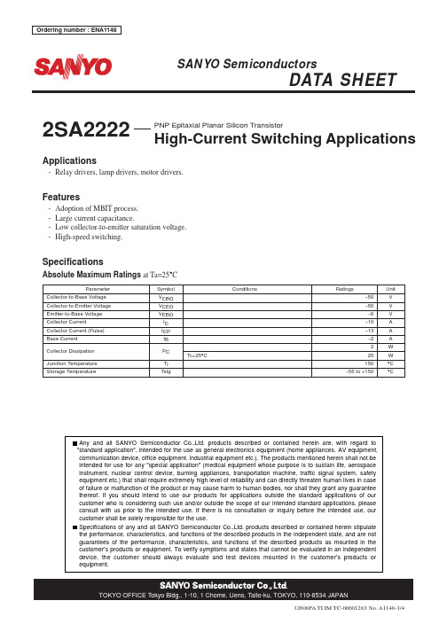
Specifications
Absolute Maximum Ratings at Ta=25°C
Parameter Collector-to-Base Voltage Collector-to-Emitter Voltage Emitter-to-Base Voltage Collector Current Collector Current (Pulse) Base Current
Applications
• Relay drivers, lamp drivers, motor drivers.
Features
• Adoption of MBIT process. • Large current capacitance. • Low collector-to-emitter saturation voltage. • High-speed switching.
--15mA --10mA
--80mA
--5mA
IB=0mA
--0.5
--1.0
--1.5
--2.0
Collector-to-Emitter Voltage, VCE -- V IT13442
No. A1148-2/4
元器件交易网
2SA2222
Collector Current, IC -- A
TOKYO OFFICE Tokyo Bldg., 1-10, 1 Chome, Ueno, Taito-ku, TOKYO, 110-8534 JAPAN
32608FA TI IM TC-00001283 No. A1148-1/4
元器件交易网
2SA2222
Electrical Characteristics at Ta=25°C
MBT2222ADW1T1G;中文规格书,Datasheet资料

VCEO VCBO VEBO
IC ESD
40
Vdc
75
Vdc
6.0
Vdc
600
mAdc
HBM Class 2 MM Class B
THERMAL CHARACTERISTICS
Characteristic
Symbol
Max
Unit
Total Package Dissipation (Note 1), TA = 25°C
© Semiconductor Components Industries, LLC, 2009
1
October, 2009 − Rev. 4
/
Publication Order Number: MBT2222ADW1T1/D
MBT2222ADW1T1G
ELECTRICAL CHARACTERISTICS (TA = 25°C unless otherwise noted) Characteristic
Output Capacitance
(VCB = 10 Vdc, IE = 0, f = 1.0 MHz)
Input Capacitance
(VEB = 0.5 Vdc, IC = 0, f = 1.0 MHz)
Inp1.0 mAdc, VCE = 10 Vdc, f = 1.0 kHz) (IC = 10 mAdc, VCE = 10 Vdc, f = 1.0 kHz)
td
−
10
ns
tr
−
25
ts
−
225
ns
tf
−
60
/
2
hFE, DC CURRENT GAIN
2N2222A中文资料
Semelab plc.
Telephone (01455) 556565. Telex: 341927. Fax (01455) 552612.
12.7 (0.500) min.
元器件交易网
LAB
ELECTRICAL CHARACTERISTICS (TA = 25°C unless otherwise stated)
Min.
40 75 6
Typ.
Max. Unit
V
V V 10 0.01 10 10 20 0.3 1 nA µA nA nA
V V
0.6 35 50 75 35 100 50 40 300
1.2 2
— 300
f = 100MHz f = 100kHz f = 100kHz f = 1kHz f = 1kHz
5.33 (0.210) 4.32 (0.170)
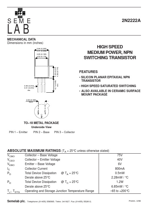
FEATURES
• SILICON PLANAR EPITAXIAL NPN TRANSISTOR • HIGH SPEED SATURATED SWITCHING • ALSO AVAILABLE IN CERAMIC SURFACE MOUNT PACKAGE
0.48 (0.019) 0.41 (0.016) dia.
2.54 (0.100) Nom.
3 2
1
TO–18 METAL PACKAGE
Underside View PIN 1 – Emitter PIN 2 – Base PIN 3 – Collector
ABSOLUTE MAXIMUM RATINGS (TA = 25°C unless otherwise stated)
KSP2222A中文资料
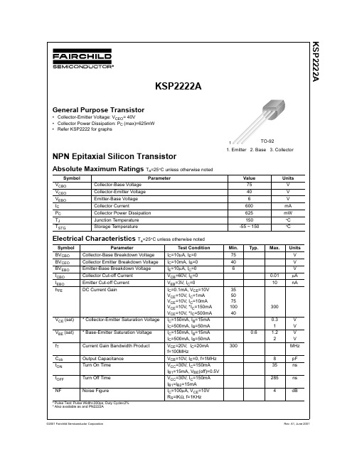
KSP2222ANPN Epitaxial Silicon TransistorAbsolute Maximum Ratings T a =25°C unless otherwise notedElectrical Characteristics T a =25°C unless otherwise noted* Pulse Test: Pulse Width ≤300µs, Duty Cycle ≤2%* Also available as and PN2222ASymbol ParameterValue Units V CBO Collector-Base Voltage 75V V CEO Collector-Emitter Voltage 40V V EBO Emitter-Base Voltage 6V I C Collector Current600mA P C Collector Power Dissipation 625mW T J Junction Temperature 150°C T STGStorage Temperature-55 ~ 150°CSymbol ParameterTest Condition Min.Typ.Max.Units BV CBO Collector-Base Breakdown Voltage I C =10µA, I E =075V BV CEO Collector Emitter Breakdown Voltage I C =10mA, I B =040V BV EBO Emitter-Base Breakdown Voltage I E =10µA, I C =06V I CBO Collector Cut-off Current V CB =60V, I E =00.01µA I EBO Emitter Cut-off Current V EB =3V, I C =010nAh FEDC Current GainI C =0.1mA, V CE =10V V CE =10V, I C =1mA V CE =10V, I C =10mA V CE =10V, *I C =150mA V CE =10V, *I C =500mA 35507510040300V CE (sat)* Collector-Emitter Saturation Voltage I C =150mA, I B =15mA I C =500mA, I B =50mA 0.31V V V BE (sat)* Base-Emitter Saturation Voltage I C =150mA, I B =15mA I C =500mA, I B =50mA 0.61.22V V f T Current Gain Bandwidth Product V CE =20V, I C =20mA f=100MHz300MHz C ob Output Capacitance V CB =10V, I E =0, f=1MHz 8pF t ON Turn On Time V CC =30V, I C =150mAI B1=15mA, V BE (off)=0.5V 35ns t OFF Turn Off Time V CC =30V, I C =150mA I B1=I B2=15mA 285ns NFNoise FigureI C =100µA, V CE =10V R S =IK Ω, f=1KHz4dBKSP2222AGeneral Purpose Transistor•Collector-Emitter Voltage: V CEO = 40V•Collector Power Dissipation: P C (max)=625mW •Refer KSP2222 for graphs1. Emitter2. Base3. CollectorTO-921KSP2222ADISCLAIMERFAIRCHILD SEMICONDUCTOR RESERVES THE RIGHT TO MAKE CHANGES WITHOUT FURTHER NOTICE TO ANY PRODUCTS HEREIN TO IMPROVE RELIABILITY, FUNCTION OR DESIGN. FAIRCHILD DOES NOT ASSUME ANY LIABILITY ARISING OUT OF THE APPLICATION OR USE OF ANY PRODUCT OR CIRCUIT DESCRIBED HEREIN;NEITHER DOES IT CONVEY ANY LICENSE UNDER ITS PATENT RIGHTS, NOR THE RIGHTS OF OTHERS.LIFE SUPPORT POLICYFAIRCHILD’S PRODUCTS ARE NOT AUTHORIZED FOR USE AS CRITICAL COMPONENTS IN LIFE SUPPORT DEVICES OR SYSTEMS WITHOUT THE EXPRESS WRITTEN APPROVAL OF FAIRCHILD SEMICONDUCTOR CORPORATION.As used herein:TRADEMARKSThe following are registered and unregistered trademarks Fairchild Semiconductor owns or is authorized to use and is not intended to be an exhaustive list of all such trademarks.1. Life support devices or systems are devices or systems which, (a) are intended for surgical implant into the body,or (b) support or sustain life, or (c) whose failure to performwhen properly used in accordance with instructions for useprovided in the labeling, can be reasonably expected to result in significant injury to the user.2. A critical component is any component of a life support device or system whose failure to perform can bereasonably expected to cause the failure of the life support device or system, or to affect its safety or effectiveness.PRODUCT STATUS DEFINITIONS Definition of TermsDatasheet Identification Product Status DefinitionAdvance InformationFormative or In Design This datasheet contains the design specifications for product development. Specifications may change in any manner without notice.PreliminaryFirst ProductionThis datasheet contains preliminary data, andsupplementary data will be published at a later date.Fairchild Semiconductor reserves the right to make changes at any time without notice in order to improve design.No Identification Needed Full ProductionThis datasheet contains final specifications. Fairchild Semiconductor reserves the right to make changes at any time without notice in order to improve design.Obsolete Not In ProductionThis datasheet contains specifications on a product that has been discontinued by Fairchild semiconductor.The datasheet is printed for reference information only.A CEx™Bottomless™CoolFET™CROSSVOLT ™DenseTrench™DOME™EcoSPARK™E 2CMOS™EnSigna™FACT™FACT Quiet Series™FAST ®FASTr™FRFET™GlobalOptoisolator™GTO™HiSeC™ISOPLANAR™LittleFET™MicroFET™MICROWIRE™OPTOLOGIC™OPTOPLANAR™PACMAN™POP™Power247™PowerTrench ®QFET™QS™QT Optoelectronics™Quiet Series™SLIENT SWITCHER ®SMART START™STAR*POWER™Stealth™SuperSOT™-3SuperSOT™-6SuperSOT™-8SyncFET™TruTranslation™TinyLogic™UHC™UltraFET ®VCX™STAR*POWER is used under license。
PMBT2222中文资料
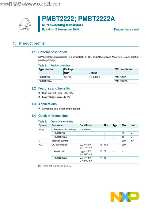
Table 8. Characteristics Tj = 25 °C unless otherwise specified.
Symbol Parameter
Conditions
Min Typ Max Unit
ICBO
collector-base cut-off
current
PMBT2222
VCB = 50 V; IE = 0 A
Conditions
VBEsat
base-emitter saturation IC = 150 mA;
voltage
IB = 15 mA
PMBT2222
PMBT2222A
base-emitter saturation IC = 500 mA;
voltage
IB = 50 mA
PMBT2222
PMBT2222A
Tamb ≤ 25 °C
[1] −65 −65
Max
Unit
60
V
75
V
30
V
40
V
5
V
6
V
600
mA
800
mA
200
mA
250
mW
150
°C
+150
°C
+150
°C
[1] Device mounted on an FR4 Printed-Circuit Board (PCB), single-sided copper, tin-plated and standard footprint.
emitter-base cut-off
VEB = 5 V; IC = 0 A
2SD2222P中文资料

100
TC=25˚C IB=1.0mA
VCE(sat) IC
IC/IB=1000
Collector power dissipation PC (W)
160 (1)
Collector current IC (A)
(1)TC=Ta (2)With a 100×100×2mm Al heat sink (3)Without heat sink (PC=3.5W)
3 500 to 10 000 5 000 to 15 000 7 000 to 20 000
at io n.
C E
Max 100 100 100 20 000 3.0 3.0
V
20.0±0.5 (2.5) Solder Dip
1: Base 2: Collector 3: Emitter TOP-3L-A1 Package
A A
Collector power dissipation
150 3.5
W
Ta = 25°C
tf o ht llow tp in :// g pa U na RL so a ni bo c. u ne t l t/s ate c/ st en in f
Internal Connection
or m
or m
at io n.
3
SJD00255BED
Request for your special attention and precautions in using the technical information and semiconductors described in this book
Collector-emitter voltage VCE (V)
2N2222 2N2222A NPN 切换管高流低压特性参数手册说明书

20736Marilla Street ChatsworthSymbolParameterMinMaxUnitsON CHARACTERISTICS*V CE(sat)Collector-Emitter Saturation Voltage8 (I C =150mAdc,I B =15mAdc)2N2222 (I C =500mAdc, I B =50mAdc)------4001.6mVdc Vdc V CE(sat)Collector-Emitter Saturation Voltage* (I C =150mAdc,I B =15mAdc)2N2222A (I C =500mAdc, I B =50mAdc)------3001.0mVdc Vdc V BE(sat)Base-Emitter Saturation Voltage * (I C =150mAdc,I B =15mAdc)2N2222 (I C =500mAdc, I B =50mAdc)------ 1.32.6Vdc Vdc V BE(sat)Base-Emitter Saturation Voltage* (I C =150mAdc,I B =15mAdc)2N2222A(I C =500mAdc, I B =50mAdc)0.6--- 1.22.0Vdc VdcSMALL-SIGNAL CHARACTERISTICSC OB Output Capacitance(V CB =10Vdc,I E =ie=0, f=1.0MHz) ---8.0pF SWITCHING CHARACTERISTICST d Delay Time---10ns t r Rise Time ---25ns t s Storage Time ---200ns t fFall TimeI CON =150mAdc,I BON =15mAdc,I B(off)=15mAdc---60ns*Pulse Test:tp Љ300us, Duty Cycle Љ2.0%2N2222,2N2222Af TTransitionFrequency(V CE =20Vdc,I C =20mAdc, f=100MHz)2N2222250---MHz 2N2222A300---MHzNFNoise Figure(V CE =5.0Vdc,I C =200µAdc, Rs=2.0KOHM,f=1.0kHz,B=200Hz)2N2222A --- 4.0dB Micro Commercial ComponentsMicro Commercial ComponentsOrdering Information :Device PackingPart Number-B P Bulk;100pcs/Box***IMPORTANT NOTICE***Micro Commercial Components Corp. reserve s the right to make changes without further notice to any product herein to make corrections, modifications , enhancements , improvements , or other changes . Micro Commercial Components Corp . does not assume any liability arising out of the application or use of any product described herein; neither does it convey any license under its patent rights ,nor the rights of others . The user of products in such applications shall assume all risks of such use and will agree to hold Micro Commercial Components Corp . and all the companies whose products are represented on our website, harmless against all damages.***LIFE SUPPORT***MCC's products are not authorized for use as critical components in life support devices or systems without the express writtenapproval of Micro Commercial Components Corporation.***CUSTOMER AWARENESS***Counterfeiting of semiconductor parts is a growing problem in the industry. Micro Commercial Components (MCC) is taking strong measures to protect ourselves and our customers from the proliferation of counterfeit parts. MCC strongly encourages customers to purchase MCC parts either directly from MCC or from Authorized MCC Distributors who are listed by country on our web page cited below. Products customers buy either from MCC directly or from Authorized MCC Distributors are genuine parts, have full traceability, meet MCC's quality standards for handling and storage. MCC will not provide any warranty coverage or other assistance for parts bought from Unauthorized Sources. MCC is committed to combat this global problem and encourage our customers to do their part in stopping this practice by buying direct or from authorized distributors.。
2N2222A中文资料_数据手册_参数
Objective specification Preliminary specification Product specification
This data sheet contains target or goal specifications for product development. This data sheet contains preliminary data; supplementary data may be published later. This data sheet contains final product specifications.
TO-18
1997 May 29
6
EUROPEAN PROJECTION
ISSUE DATE 97-04-18
Philips Semiconductors
NPN switching transistors
Product specification
2N2222; 2N2222A
DEFINITIONS
Data sheet status
SYMBOL
PARAMETER
Rth j-a Rth j-c
thermal resistance from junction to ambient thermal resistance from junction to case
CONDITIONS in free air
MIN.
MAX.
UNIT
−
60
Product specification
2N2222; 2N2222A
LIMITING VALUES In accordance with the Absolute Maximum Rating System (IEC 134).
飞利浦 PXT2222A 数据手册

DATA SHEETProduct specificationSupersedes data of 1997May 051999Apr 14PXT2222ANPN switching transistorbook, halfpageM3D109查询PXT2222供应商NPN switching transistorPXT2222AFEATURES•High current (max. 600mA)•Low voltage (max. 40V).APPLICATIONS•General purpose switching and linear amplification.DESCRIPTIONNPN switching transistor in a SOT89 plastic package.PNP complement: PXT2907A.MARKINGTYPE NUMBER MARKING CODEPXT2222Ap1PPINNINGPIN DESCRIPTION1emitter 2collector 3baseFig.1 Simplified outline (SOT89) and symbol.handbook, halfpage123Bottom viewMAM296321LIMITING VALUESIn accordance with the Absolute Maximum Rating System (IEC 134).Note1.Device mounted on a printed-circuit board, single-sided copper, tinplated, mounting pad for collector 6cm2.For other mounting conditions, see “Thermal considerations for SOT89 in the General Part of associated Handbook”.SYMBOL PARAMETERCONDITIONSMIN.MAX.UNITV CBO collector-base voltage open emitter −75V V CEO collector-emitter voltage open base −40V V EBO emitter-base voltage open collector−6V I C collector current (DC)−600mA I CM peak collector current −800mA I BM peak base current −200mA P tot total power dissipation T amb ≤25°C; note 1− 1.25W T stg storage temperature −65+150°C T j junction temperature−150°C T amb operating ambient temperature−65+150°CNPN switching transistorPXT2222ATHERMAL CHARACTERISTICS Note1.Device mounted on a printed-circuit board, single-sided copper, tinplated, mounting pad for collector 6cm2.For other mounting conditions, see “Thermal considerations for SOT89 in the General Part of associated Handbook”.CHARACTERISTICST j =25°C unless otherwise specified.SYMBOL PARAMETERCONDITIONS VALUE UNIT R th j-a thermal resistance from junction to ambient note 1100K/W R th j-s thermal resistance from junction to soldering point20K/WSYMBOL PARAMETERCONDITIONSMIN.MAX.UNIT I CBO collector cut-off current I E =0; V CB =60V−10nA I E =0; V CB =60V; T amb =125°C −10µA I EBO emitter cut-off current I C =0; V BE =5V −10nAh FEDC current gainI C =0.1mA; V CE =10V 35−I C =1mA; V CE =10V 50−I C =10mA; V CE =10V75−I C =10mA; V C =10V; T amb =−55°C 35−I C =150mA; V CE =1V 50−I C =150mA; V CE =10V 100300I C =500mA; V CE =10V40−V CEsat collector-emitter saturation voltageI C =150mA; I B =15mA −300mV I C =500mA; I B =50mA −1V V BEsat base-emitter saturation voltage I C =150mA; I B =15mA 0.6 1.2V I C =500mA; I B =50mA −2V C c collector capacitance I E =i e =0; V CB =10V; f =1MHz −8pF C e emitter capacitance I C =i c =0; V EB =500mV; f =1MHz −25pF f T transition frequency I C =20mA; V CE =10V; f =100MHz 300−MHz Fnoise figureI C =200µA; V CE =5V; R S =2k Ω;f =1kHz; B =200Hz −4dB Switching times (between 10% and 90% levels);(see Fig.2)t on turn-on time I Con =150mA; I Bon =15mA;I Boff =−15mA−35ns t d delay time −15ns t r rise time −20ns t off turn-off time −250ns t s storage time −200ns t ffall time−60nsNPN switching transistor PXT2222Ahandbook, full pagewidthR CR2R1DUTMLB826V oR B(probe)450 Ω(probe)450 ΩoscilloscopeoscilloscopeV BB V iV CCFig.2 Test circuit for switching times.V i =9.5V; T =500µs; t p =10µs; t r =t f ≤3ns.R1=68Ω; R2=325Ω; R B =325Ω; R C =160Ω.V BB =−3.5V; V CC =29.5V.Oscilloscope: input impedance Z i =50Ω.NPN switching transistorPXT2222APACKAGE OUTLINEREFERENCESOUTLINE VERSION EUROPEAN PROJECTIONISSUE DATE IECJEDECEIAJDIMENSIONS (mm are the original dimensions) SOT8997-02-28w Me 1eEH EB02 4 mmscaleb 3b 2b 1cD LAPlastic surface mounted package; collector pad for good heat transfer; 3 leadsSOT89123UNIT A mm1.61.40.480.35c 0.440.37D 4.64.4E 2.62.4H E 4.253.75e 3.0w 0.13e 11.5L min.0.8b 2b 10.530.40b 31.81.4NPN switching transistor PXT2222ADEFINITIONSData sheet statusObjective specification This data sheet contains target or goal specifications for product development. Preliminary specification This data sheet contains preliminary data; supplementary data may be published later. Product specification This data sheet contains final product specifications.Limiting valuesLimiting values given are in accordance with the Absolute Maximum Rating System (IEC 134). Stress above one or more of the limiting values may cause permanent damage to the device. These are stress ratings only and operation of the device at these or at any other conditions above those given in the Characteristics sections of the specification is not implied. Exposure to limiting values for extended periods may affect device reliability.Application informationWhere application information is given, it is advisory and does not form part of the specification.LIFE SUPPORT APPLICATIONSThese products are not designed for use in life support appliances, devices, or systems where malfunction of these products can reasonably be expected to result in personal injury. Philips customers using or selling these products for use in such applications do so at their own risk and agree to fully indemnify Philips for any damages resulting from such improper use or sale.NPN switching transistor PXT2222ANOTESInternet: Philips Semiconductors – a worldwide company© Philips Electronics N.V. 1999SCA63All rights are reserved. Reproduction in whole or in part is prohibited without the prior written consent of the copyright owner.The information presented in this document does not form part of any quotation or contract, is believed to be accurate and reliable and may be changed without notice. No liability will be accepted by the publisher for any consequence of its use. Publication thereof does not convey nor imply any license under patent- or other industrial or intellectual property rights.Netherlands: Postbus 90050, 5600PB EINDHOVEN, Bldg.VB,Tel.+31402782785,Fax.+31402788399New Zealand: 2Wagener Place, C.P.O.Box 1041, AUCKLAND,Tel.+6498494160,Fax.+6498497811Norway: Box 1, Manglerud 0612, OSLO,Tel.+4722748000,Fax.+4722748341Pakistan: see SingaporePhilippines: Philips Semiconductors Philippines Inc.,106Valero St.Salcedo Village, P.O.Box 2108MCC,MAKATI,Metro MANILA, Tel.+6328166380,Fax.+6328173474Poland: Ul.Lukiska 10, PL 04-123WARSZAWA,Tel.+48226122831,Fax.+48226122327Portugal: see Spain Romania: see ItalyRussia: Philips Russia, atcheva 35A, 119048MOSCOW,Tel.+70957556918,Fax.+70957556919Singapore: Lorong 1, Toa Payoh, SINGAPORE 319762,Tel.+653502538,Fax.+652516500Slovakia: see Austria Slovenia: see ItalySouth Africa: S.A. PHILIPS Pty Ltd., 195-215Main Road Martindale,2092JOHANNESBURG, P.O.Box 7430 Johannesburg 2000,Tel.+27114705911,Fax.+27114705494South America: Al.Vicente Pinzon,173, 6th floor,04547-130SÃO PAULO,SP, Brazil,Tel.+55118212333,Fax.+55118212382Spain: Balmes 22, 08007BARCELONA,Tel.+34933016312,Fax.+34933014107Sweden: Kottbygatan 7, Akalla, S-16485STOCKHOLM,Tel.+46859852000,Fax.+46859852745Switzerland: Allmendstrasse 140, CH-8027ZÜRICH,Tel.+4114882741Fax.+4114883263Taiwan: Philips Semiconductors, 6F, No.96, Chien Kuo N.Rd.,Sec.1,TAIPEI, Taiwan Tel.+886221342886,Fax.+886221342874Thailand: PHILIPS ELECTRONICS (THAILAND) Ltd.,209/2Sanpavuth-Bangna Road Prakanong, BANGKOK 10260,Tel.+6627454090,Fax.+6623980793Turkey: Talatpasa Cad. No.5, 80640GÜLTEPE/ISTANBUL,Tel.+902122792770,Fax.+902122826707Ukraine : PHILIPS UKRAINE, 4Patrice Lumumba str., Building B, Floor 7,252042KIEV, Tel.+380442642776, Fax. +380442680461United Kingdom: Philips Semiconductors Ltd., 276Bath Road, Hayes,MIDDLESEX UB35BX, Tel.+441817305000,Fax.+441817548421United States: 811East Arques Avenue, SUNNYVALE, CA 94088-3409,Tel.+18002347381, Fax.+18009430087Uruguay: see South AmericaVietnam: see SingaporeYugoslavia: PHILIPS, Trg N. Pasica 5/v, 11000BEOGRAD,Tel.+38111625344,Fax.+38111635777For all other countries apply to: Philips Semiconductors,International Marketing &Sales Communications,Building BE-p, P.O.Box 218,5600MD EINDHOVEN, The Netherlands,Fax.+31402724825Argentina: see South AmericaAustralia: 34 Waterloo Road, NORTH RYDE, NSW 2113,Tel.+61298054455,Fax.+61298054466Austria:Computerstr. 6, A-1101 WIEN, P.O. Box 213,Tel.+431601011248, Fax.+431601011210Belarus: Hotel Minsk Business Center, Bld.3, r.1211, Volodarski Str.6,220050MINSK, Tel.+375172200733,Fax.+375172200773Belgium: see The Netherlands Brazil:see South AmericaBulgaria:Philips Bulgaria Ltd., Energoproject, 15th floor,51James Bourchier Blvd., 1407SOFIA,Tel.+3592689211,Fax.+3592689102Canada: PHILIPS SEMICONDUCTORS/COMPONENTS,Tel.+18002347381, Fax.+18009430087China/Hong Kong: 501Hong Kong Industrial Technology Centre,72Tat Chee Avenue, Kowloon Tong, HONG KONG,Tel.+852********,Fax.+852********Colombia: see South America Czech Republic: see AustriaDenmark: Sydhavnsgade 23, 1780COPENHAGEN V,Tel.+4533293333,Fax.+4533293905Finland: Sinikalliontie 3, FIN-02630ESPOO,Tel.+3589615800,Fax.+358961580920France: 51Rue Carnot, BP317, 92156SURESNES Cedex,Tel.+33140996161,Fax.+33140996427Germany: Hammerbrookstraße 69, D-20097HAMBURG,Tel.+4940235360,Fax.+494023536300Hungary:see AustriaIndia: Philips INDIA Ltd, Band Box Building, 2nd floor,254-D,Dr.Annie Besant Road, Worli, MUMBAI 400025,Tel.+91224938541,Fax.+91224930966Indonesia: PT Philips Development Corporation, Semiconductors Division,Gedung Philips, Jl. Buncit Raya Kav.99-100, JAKARTA 12510,Tel.+62217940040ext.2501, Fax.+62217940080Ireland: Newstead, Clonskeagh, DUBLIN 14,Tel.+35317640000,Fax.+35317640200Israel: RAPAC Electronics, 7Kehilat Saloniki St, PO Box 18053,TEL AVIV 61180, Tel.+97236450444,Fax.+97236491007Italy: PHILIPS SEMICONDUCTORS, Piazza IV Novembre 3,20124MILANO, Tel.+39267522531,Fax.+39267522557Japan: Philips Bldg 13-37, Kohnan 2-chome, Minato-ku,TOKYO 108-8507, Tel.+81337405130,Fax.+81337405077Korea: Philips House, 260-199Itaewon-dong, Yongsan-ku, SEOUL,Tel.+8227091412,Fax.+8227091415Malaysia: No.76Jalan Universiti, 46200PETALING JAYA, SELANGOR,Tel.+60 37505214,Fax.+6037574880Mexico: 5900Gateway East, Suite 200, EL PASO, TEXAS 79905,Tel.+9-58002347381, Fax +9-58009430087Middle East: see ItalyPrinted in The Netherlands115002/00/03/pp8 Date of release: 1999Apr 14Document order number: 939775005635。
- 1、下载文档前请自行甄别文档内容的完整性,平台不提供额外的编辑、内容补充、找答案等附加服务。
- 2、"仅部分预览"的文档,不可在线预览部分如存在完整性等问题,可反馈申请退款(可完整预览的文档不适用该条件!)。
- 3、如文档侵犯您的权益,请联系客服反馈,我们会尽快为您处理(人工客服工作时间:9:00-18:30)。
SBT2222AF v
S e m i c o n d u c t o r
NPN Silicon Transistor
SBT2222AF
Absolute maximum ratings Ta=25°C
Characteristic Symbol Ratings Unit
Collector-Base voltage V CBO 75 V Collector-Emitter voltage V CEO 40 V
Emitter-base voltage V EBO 5 V
Collector current I C 600 mA Collector dissipation P C * 350 mW
Junction temperature T j 150 °C Storage temperature range
T stg -55~150 °C
* : Package mounted on 99.5% alumina 10×8×0.6mm
Electrical Characteristics Ta=25°C
Characteristic Symbol
Test Condition Min. Typ. Max.Unit
Collector-Base breakdown voltage BV CBO I C =10µA, I E =0
75 - - V
Collector-Emitter breakdown voltage BV CEO
I C =1mA, I B =0 40
- - V Emitter-Base breakdown voltage BV EBO I E =10µA, I C =0 5 - - V Collector cut-off current I CBO V CB =75V , I E =
0 - - 20 nA
DC current gain
h FE V CE =10V , I C =10mA 100 - - -
Collector-Emitter saturation voltage V CE(sat) I C =150mA, I B =15mA - - 0.4 V
Transition frequency
f T V CE =20V , I C =20mA,
f=100MHz
250 - - MHz Collector output capacitance C ob
V CB =10V , I E =0, f=1MHz
-
-
8
pF
Delay time t d - - 10 ns Rise time t r
V CC =30V dc , V BE(off)=0.5V dc , I C =150mA dc , I B1=15mA dc - - 25 ns Storage time t s - - 225 ns Fall Time
t f
V CC =30V dc ,I C =150mA dc , I B1=I B2=15mA dc - - 60 ns
SBT2222AF
Electrical Characteristic Curves
SBT2222AF
These AUK products are intended for usage in general electronic equipments(Office and communication equipment, measuring equipment, domestic electrification, etc.).
Please make sure that you consult with us before you use these AUK products in equipm-ents which require high quality and/or reliability, and in equipments which could have major impact to the welfare of human life(atomic energy control, airplane, spaceship, traffic signal, combustion central, all types of safety device, etc.).
AUK cannot accept liability to any damage which may occur in case these AUK products were used in the mentioned equipments without prior consultation with AUK.。
